US8110883B2 - Electromagnetic and thermal sensors using carbon nanotubes and methods of making same - Google Patents
Electromagnetic and thermal sensors using carbon nanotubes and methods of making sameDownload PDFInfo
- Publication number
- US8110883B2 US8110883B2US12/046,855US4685508AUS8110883B2US 8110883 B2US8110883 B2US 8110883B2US 4685508 AUS4685508 AUS 4685508AUS 8110883 B2US8110883 B2US 8110883B2
- Authority
- US
- United States
- Prior art keywords
- nanotube
- detector
- fabric
- nanotube fabric
- electromagnetic radiation
- Prior art date
- Legal status (The legal status is an assumption and is not a legal conclusion. Google has not performed a legal analysis and makes no representation as to the accuracy of the status listed.)
- Active, expires
Links
Images


Classifications
- G—PHYSICS
- G01—MEASURING; TESTING
- G01T—MEASUREMENT OF NUCLEAR OR X-RADIATION
- G01T1/00—Measuring X-radiation, gamma radiation, corpuscular radiation, or cosmic radiation
- G01T1/16—Measuring radiation intensity
- G—PHYSICS
- G01—MEASURING; TESTING
- G01J—MEASUREMENT OF INTENSITY, VELOCITY, SPECTRAL CONTENT, POLARISATION, PHASE OR PULSE CHARACTERISTICS OF INFRARED, VISIBLE OR ULTRAVIOLET LIGHT; COLORIMETRY; RADIATION PYROMETRY
- G01J5/00—Radiation pyrometry, e.g. infrared or optical thermometry
- G01J5/02—Constructional details
- G01J5/0225—Shape of the cavity itself or of elements contained in or suspended over the cavity
- G01J5/023—Particular leg structure or construction or shape; Nanotubes
- G—PHYSICS
- G01—MEASURING; TESTING
- G01J—MEASUREMENT OF INTENSITY, VELOCITY, SPECTRAL CONTENT, POLARISATION, PHASE OR PULSE CHARACTERISTICS OF INFRARED, VISIBLE OR ULTRAVIOLET LIGHT; COLORIMETRY; RADIATION PYROMETRY
- G01J5/00—Radiation pyrometry, e.g. infrared or optical thermometry
- G01J5/02—Constructional details
- G01J5/08—Optical arrangements
- G01J5/0846—Optical arrangements having multiple detectors for performing different types of detection, e.g. using radiometry and reflectometry channels
- G—PHYSICS
- G01—MEASURING; TESTING
- G01J—MEASUREMENT OF INTENSITY, VELOCITY, SPECTRAL CONTENT, POLARISATION, PHASE OR PULSE CHARACTERISTICS OF INFRARED, VISIBLE OR ULTRAVIOLET LIGHT; COLORIMETRY; RADIATION PYROMETRY
- G01J5/00—Radiation pyrometry, e.g. infrared or optical thermometry
- G01J5/02—Constructional details
- G01J5/08—Optical arrangements
- G01J5/0853—Optical arrangements having infrared absorbers other than the usual absorber layers deposited on infrared detectors like bolometers, wherein the heat propagation between the absorber and the detecting element occurs within a solid
- G—PHYSICS
- G01—MEASURING; TESTING
- G01J—MEASUREMENT OF INTENSITY, VELOCITY, SPECTRAL CONTENT, POLARISATION, PHASE OR PULSE CHARACTERISTICS OF INFRARED, VISIBLE OR ULTRAVIOLET LIGHT; COLORIMETRY; RADIATION PYROMETRY
- G01J5/00—Radiation pyrometry, e.g. infrared or optical thermometry
- G01J5/10—Radiation pyrometry, e.g. infrared or optical thermometry using electric radiation detectors
- G01J5/20—Radiation pyrometry, e.g. infrared or optical thermometry using electric radiation detectors using resistors, thermistors or semiconductors sensitive to radiation, e.g. photoconductive devices
- G01J5/22—Electrical features thereof
- G01J5/24—Use of specially adapted circuits, e.g. bridge circuits
- G—PHYSICS
- G01—MEASURING; TESTING
- G01J—MEASUREMENT OF INTENSITY, VELOCITY, SPECTRAL CONTENT, POLARISATION, PHASE OR PULSE CHARACTERISTICS OF INFRARED, VISIBLE OR ULTRAVIOLET LIGHT; COLORIMETRY; RADIATION PYROMETRY
- G01J5/00—Radiation pyrometry, e.g. infrared or optical thermometry
- G01J5/02—Constructional details
- G01J5/04—Casings
- G01J5/046—Materials; Selection of thermal materials
Definitions
- the present applicationrelates generally to nanotube fabrics and methods of making same and, more specifically to carbon nanotube fabrics and methods of making same for use in electromagnetic radiation detecting and sensing systems.
- Detectorsare an integral part of optical circuits and components (emitters, modulators, repeaters, waveguides or fibers, reflectors, resonators, etc.) and are used for the sensing of electromagnetic (EM) radiation.
- Photoconducting materialstypically semiconductors, have electrical properties that vary when exposed to EM radiation (i.e. UV, visible and IR).
- One type of photoconductivityarises from the generation of mobile carriers (electrons or holes) during absorption of photons.
- p-n diodep-i-n photodiode, avalanche photodiode, etc.
- p-i-n photodiodep-i-n photodiode
- avalanche photodiodeetc.
- Light detectionis ideally suited for direct band gap semiconductors such as Ge, GaAs, etc.; however, indirect band gap semiconductors (where an additional phonon energy is required to excite an electron from the valence band to the conduction band, making these detectors less efficient), such as Silicon, are also used as photodetectors.
- photodetctora simple p-n diode or Schottky barrier to detect impinging photons.
- siliconmost photodetectors do not integrate with current microelectronics technology, usually detect only a specific wavelength (i.e. 1.1 ⁇ m for Si, 0.87 ⁇ m for GaAs, 0.414 ⁇ m for ⁇ -SiC and 1.89 ⁇ m for Ge), and require multiple detectors to detect a broad band of wavelengths (hence photon energy).
- Bolometerscan be constructed from either metallic, metallic-oxides or semiconducting materials. Since bolometers detect a broad range of radiation above a few microns, bolometers are typically cryogenically cooled to reduce the detection of blackbody radiation that is emitted from the detector material, which leads to a high background noise.
- Detectorsare critical for communication and EM sensing applications, specifically in the infrared (IR) spectrum, ⁇ >0.75 ⁇ m.
- IR sensorsare expensive, require advanced fabrication techniques that are not compatible with Si—CMOS technology, have limited resolution and do not operate at room temperature (hence require cooling).
- Conventional IR detectorsmainly employ bolometers, more specifically microbolometers.
- IRFPAsIR Focal Plane Arrays
- VOxvanadium dioxide
- tactical and strategic applicationshad relied upon HgCdTe IRFPAs, which operated at 77 K and necessitated the use of mechanical coolers.
- the HgCdTe systemwas plagued by defects, high processing costs, low yields and substantial weight (eliminating crucial man-portable applications).
- VOxserving as the TCR (Temperature Coefficient of Resistance) IR radiation sensing layer that is deposited on a thermally isolated cantilever beam, based microbolometers overcame many of the issues associated with HgCdTe.
- VOx technologycan be fabricated with CMOS design and process technologies on silicon wafers, with a lower built in unit product cost. VOx devices also do not require cooling to 77 K—only thermal stabilization. This technology also enabled the introduction of man portable IR systems such as Thermal Weapon Sight and helmet integrated visible/Long-Wave IR (8-12 ⁇ m) fused imagery, which would not have been possible with cooled HgCdTe.
- CMOS compatibilityprovides improved performance and increased resolution.
- Advanced CMOS processing techniquesalso enables the development of a reflective cavity coating that allows IR energy to reflect off the bottom of a cavity and to be absorbed by the VOx layer, increasing the efficiency of IR adsorption.
- detector unit cellshave shrunk and the fill factors have increased, resulting in 640 ⁇ 480 pixel IRFPAs, thereby increasing the resolution of the cameras that these IRFPA are deployed in.
- the resolution of the IRFPAis directly related to the CMOS technology node and the minimum pixel size of the bolometer.
- VOxhas contributed to microbolometers, there is evidence that the improvement curve for this material is slowing down and some fundamental limits are preventing the use of these arrays in modern IR systems.
- MWIRvital Mid-Wave IR
- a second limitationis that for UV applications, such as threat warning of missiles, VOx technology is not able to detect UV signatures from missile plumes.
- thermal isolationhas improved to the levels of 20 mK, further improvements are required; therefore, another limitation of VOx based IRFPAs is that the performance Noise Equivalent Temperature Difference (NETD) is saturating, related to the limits of VOx absorption.
- NETDNoise Equivalent Temperature Difference
- VOx based microbolometersAnother issue with VOx is the inability to scale below 25 micron pixel sizes, limiting detectors to 640 ⁇ 480 pixels. As stated above, below 25 microns, the TCR of VOx becomes non-linear. Additionally, the 1/f noise of VOx increases as the pixel dimension decreases.
- Carbon nanotubesare a promising material for electromagnetic (EM) detection and have recently been investigated for their unique optical properties, focusing on the emission and detection of IR radiation (see Sheng, et al., “Exciton dynamics in single-walled nanotubes: Transient photoinduced dichroism and polarized emission,” Physical Review B, 71 (2005), 125427, Perebeinos, et al., “Scaling of Excitons in Carbon Nanotubes,” Physical Review Letters, 92 (2004), 257402, Ugawa, et al., “Far-infrared to visible optical conductivity of single-wall carbon nanotubes,” Current Applied Physics, 1 (2001) 485-491, Lehman, et al., “Single-wall carbon nanotube coating on a pyroelectric detector,” Applied Optics, 44 (2005), 483-488, Itkis, et al., “Bolometric infrared photoresponse of suspended single-walled carbon nano
- Typical band-gaps for carbon nanotubesrange from 0.6-1.2 eV, depending on the diameter of the CNT, where the band gap is inversely proportional to the diameter of the nanotube, which correlates to detection and emission of radiation in the IR spectrum.
- CNT light emission and detectionnamely the generation of excitons to produce a photocurrent or the generation of heat which changes the resistance of nanotube material (bolometer).
- Photoluminescence and photo-detection studieshave demonstrated that carbon nanotubes, specifically single-walled nanotubes (SWNTs), absorb radiation at between 0.6-2 eV, correlating to the transition between van Hove peaks of the nanotubes (S11, S22 and M11).
- Carbon nanotubeshave also demonstrated extremely high absorption coefficients of the order of 10 4 -10 5 cm ⁇ 1 , higher than HgCdTe and much higher than VOx. Combining these properties allows for CNTs as a possible candidate for replacing HgCdTe and VOx for resistive microbolometer material.
- a paper by Itkisdemonstrated the creation a non-CMOS compatible CNT bolometer using a thick suspended mat of as-deposited, arc-grown SWNTs.
- the mat of CNTsdemonstrated a sizable decrease in conductivity of the CNT mat with an S/N ratio of 100.
- TCR values measured by Itkisare comparable to vanadium dioxide, which strongly suggests the ability of the CNT bolometer to operate at room temperature. It was also noted that a decrease in mat thickness improves the sensitivity of the CNT bolometer; however, their fabrication technique can not produce reliable thickness and is not scalable to monolayered fabrics.
- the present applicationrelates generally to nanotube fabrics and methods of making same and, more specifically to carbon nanotube fabrics and methods of making same for use in electromagnetic radiation detecting and sensing systems.
- electromagnetic and thermal sensors and detectors using carbon nanotube fabricsare provided.
- microbolometers using carbon nanotubes and carbon nanotube fabricsare used to detect UV and IR radiation.
- an electromagnetic radiation detectorincludes a substrate, a nanotube fabric disposed on the substrate, the nanotube fabric comprising a non-woven network of nanotubes, and first and second conductive terminals, each in electrical communication with the nanotube fabric, the first and second conductive terminals disposed in space relation to one another.
- the nanotube fabricmay be tuned to be sensitive to a predetermined range of electromagnetic radiation such that exposure to the electromagnetic radiation induces a change in impedance between the first and second conductive terminals.
- the detectorfurther includes sensing circuitry for detecting the change in input impedance, the sensing circuitry integrated with CMOS circuitry.
- the nanotube fabricis functionalized to be sensitive to the predetermined range of electromagnetic radiation.
- the nanotube fabricis derivatized to be sensitive to the predetermined range of electromagnetic radiation.
- the substratecomprises a dielectric material.
- a predetermined range of electromagnetic radiationincludes IR radiation and the active region of the nanotube fabric has a thermal coefficient of resistance between approximately 1% per degree C. and approximately 4% per degree C.
- the electromagnetic radiationcomprises UV radiation.
- the nanotube fabriccomprises one of a multilayer fabric and a monolayer fabric.
- the nanotube fabricfurther comprises semiconducting nanoparticles, the nanotube fabric tuned such that exposure to a selected photon energy induces the change in impedance between the first and second conductive terminals.
- the nanotube fabriccomprises dye-sensitized nanoparticles.
- the nanotube fabriccomprises electromagnetic radiation-sensitive nanoparticles including at least one of VOx, amorphous silicon and Ti particles.
- the nanotube fabricis disposed on a dielectric layer and the nanotube fabric comprises an active region that is suspended in spaced relation from the substrate.
- a reflective layeris disposed in spaced relation from the active region of the nanotube fabric and defines a boundary of a cavity, the reflective layer reflecting at least a portion of the electromagnetic radiation such that the reflected electromagnetic radiation is incident on the active region of the nanotube fabric.
- the predetermined range of electromagnetic radiationcomprises thermal radiation and the nanotube fabric is tuned to have a selected thermal coefficient of resistance (TCR).
- TCRthermal coefficient of resistance
- the TCRcomprises a positive value.
- the TCRcomprises a negative value.
- the selected TCRis tuned through one of doping and functionalizing the nanotube fabric.
- a microbolometer detectorincludes a substrate, a conductive electrode, a reflective element having an upper surface substantially disposed below the upper surface of the substrate, the reflective element defining at least one boundary of a cavity in the substrate and a dielectric layer disposed over at least a portion of the cavity and disposed over the conductive electrode.
- the microbolometerfurther includes a region of nanotube fabric comprising a non-woven network of nanotubes disposed on the dielectric layer and in electrical communication with the conductive electrode and the region of nanotube fabric is tuned to be sensitive to a predetermined range of electromagnetic radiation such that exposure to the electromagnetic radiation induces in the nanotube fabric electrical stimuli transmitted to the conductive electrode.
- the nanotube fabricis functionalized with electromagnetic radiation-sensitive particles to induce the electrical stimulus in the nanotube fabric.
- the dielectric layerincludes a material substantially transparent to electromagnetic radiation in the IR range.
- the dielectric layerincludes a doped SiNx material.
- the dielectric layercomprises a low-stress SiNx material.
- the detectorfurther includes sensing circuitry for detecting the electrical stimuli transmitted to the conductive electrode, the sensing circuitry integrated with CMOS circuitry.
- the reflective elementsubstantially reflects electromagnetic radiation such that the nanotube fabric absorbs electromagnetic radiation incident on the detector and reflected electromagnetic radiation.
- the reflected electromagnetic radiation incident on the nanotube fabriccomprises approximately 20% of electromagnetic radiation absorbed by the nanotube fabric.
- the electromagnetic radiationcomprises IR radiation and the nanotube fabric is tuned to have an absorption coefficient of approximately 10E4 cm-1 to approximately 10E5 cm-1.
- the region of nanotube fabricis tuned to have a sheet resistance of approximately 100 to 10000 ohms per square.
- the region of nanotube fabriccomprises an area between approximately 25 microns square and approximately 2500 microns square.
- the conductive electrodecomprises a Co material.
- the conductive electrodecomprises a Ti material.
- the microbolometer detectorfurther includes a second conductive electrode in electrical communication with the region of nanotube fabric, the second conductive electrode disposed in spaced relation to the first conductive electrode.
- the conductive electrode and the second conductive electrodecomprise one of a ZnO material, a GaN material, and a Si3N4 material, the conductive electrode and second conductive electrode in electrical communication with CMOS circuitry.
- the nanotube fabricfurther comprises semiconducting nanoparticles, the nanotube fabric tuned to be sensitive to a predetermined photon energy.
- the nanotube fabricfurther comprises dye-sensitized nanoparticles.
- the detectoris in electrical communication with interconnect circuitry and the nanotube fabric is tuned such that a first impedance value between the first and second conductive terminals matches an impedance of the interconnect circuitry.
- a method of making an electromagnetic radiation detectorincludes providing a substrate, providing a conductive electrode, providing a nanotube fabric comprising a non-woven network of nanotubes, disposed in electrical communication with the conductive electrode and forming a cavity in the substrate such that a portion of the region of nanotube fabric is suspended over the cavity.
- the methodfurther includes forming a nanotube detector member from the nanotube fabric, the nanotube detector member tuned to be sensitive to a selected range of electromagnetic radiation such that exposure to the electromagnetic radiation induces in the detector member a change in electrical stimuli communicated to the conductive electrode.
- providing the nanotube fabricincludes providing substantially purified nanotubes and forming the nantotube detector member includes patterning the nanotube fabric.
- forming the nanotube detector membercomprises one of functionalizing and derivitizing the nanotube fabric.
- a reflective elementmay be formed on a surface of the substrate, the reflective element defining a lower boundary of the cavity.
- the reflective elementincludes a material selected to reflect a subset of the electromagnetic radiation.
- a dielectric layermay be disposed on least a portion of the cavity in the substrate and disposed over the conductive electrode, the dielectric layer interposed between the conductive electrode and the nanotube detector member.
- forming the cavity in the substratefurther comprises providing a sacrificial layer and selectively removing a portion of the substrate.
- the sacrificial layerincludes one of amorphous silicon, aluminum, germanium and thermally decomposing polymer.
- the region of nanotube fabricincludes one of spinning or spray coating carbon nanotubes such that the region of nanotube fabric has a sheet resistance of approximately 100 to 10000 ohms per square.
- providing the region of nanotube fabricfurther comprises an annealing process to eliminate at least some metallic nanotubes.
- a gate electrode in electrical communication with the nanotube fabricmay be formed for gating at least some semiconducting nanotubes in the nanotube fabric.
- the region of nanotube fabricmay be tuned to reduce 1/f noise in electrical stimulus communicated to the conductive contact.
- the substrate, conductive electrode and region of nanotube fabricmay be mounted in a partial vacuum package and the partial vacuum package may be back-filled with a selected gas, the selected gas He.
- a broad-range electromagnetic radiation detector array on a waferincludes a plurality of detectors.
- Each detectormay have a substrate, a nanotube fabric disposed on the substrate, the nanotube fabric comprising a non-woven network of nanotubes, and first and second conductive terminals, each in electrical communication with the nanotube fabric, the first and second conductive terminals disposed in space relation to one another.
- Each detector in the arraymay be tuned to be sensitive to a predetermined subset of a broad-range of electromagnetic radiation such that exposure to the predetermined subset of electromagnetic radiation induces in each detector a change in impedance between the first and second conductive terminals.
- the predetermined subset of the broad-range of electromagnetic radiationincludes the UV range.
- the predetermined subset of the broad-range of electromagnetic radiationincludes the IR range.
- electromagnetic radiationincludes thermal radiation and tuning each detector includes tuning the TCR of the nanotube fabric.
- tuning the TCR of the nanotube fabricincludes adjusting the thickness of the layer of nanotubes.
- a cavityis fabricated in an oxide after interconnect metals of a CMOS wafer are processed.
- a thin film dielectric member that is thermally isolated from the surrounding environmentmay be provided.
- a nanotube fabricmay be placed on the dielectric member having, in certain embodiments, either a positive or negative TCR of approximately 1-2.5%.
- a sacrificial layermay be used to create a cantilever beam pixel structure.
- the cantilever beam pixel structuremay be connected to conductive contacts which are, in turn, connected to the terminal metallurgy of the CMOS circuits.
- a sacrificial layermay be used to form a cavity that consists of amorphous silicon, aluminum or thermally decomposing polymer.
- the conductive contactscomprise Si3N4 Legs provide connections to terminal metallurgy of corresponding CMOS wafers for detectors sensitive to at least a portion of IR radiation.
- conductive contactscomprise highly doped ZnO legs provide connections to terminal metallurgy of corresponding CMOS wafers for detectors sensitive to at least a portion of UV radiation.
- a carbon nanotube layercomprises semiconducting nanotubes fabricated with an anneal process that substantially eliminates metallic nanotubes.
- a reflective thin filmis included to increase the absorption of incident radiation from approximately 70% to 90%.
- readout electronic preamplifier circuitryis based upon capacitive trans-impedance input architecture designed in CMOS.
- the digital readout sectionmay also be designed to readout the rows and columns of two dimensional pixel arrays.
- the circuitrycomprises integrators, sample and hold and column multiplexers.
- the detectorsare tuned to absorb radiation in the IR bands, especially LWIR (8-12 microns) and MWIR (3-5 microns) and in the UV range.
- Multicolor focal plane arraysare with near simultaneous readout of detectors are provided.
- Thermistor sensors using carbon nanotubesare provided under other embodiments.
- microbolometers with carbon nanotube fabricsinclude thermal stabilization or a thermal reference for calibration.
- Focal plane arrayscan use either a single stage thermoelectric stabilizer or incorporate memory into the electronic design to calibrate each pixel at test.
- dye sensitized solar cells using carbon nanotubesare provided.
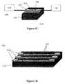
- FIG. 1Aillustrates a detecting element according to one aspect of the invention with a suspended nanofabric
- FIG. 1Billustrates an array of detecting elements according to certain aspects of the invention with a suspended nanofabric
- FIG. 1Cillustrates a detection element according to one aspect of the invention with a non-suspended nanofabric
- FIG. 1Dillustrates an array of detecting elements according to certain aspects of the invention with a non-suspended nanofabric
- FIG. 2illustrates nanofabric photodiode
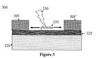
- FIG. 3illustrates a nanofabric photo-acoustic detector
- FIG. 4illustrates Wheatstone bridge photodetector circuitry
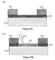
- FIGS. 5A and 5Billustrate a nanofabric bolometer
- FIG. 6Aillustrates a nanofabric detector with attached photosensing materials
- FIG. 6Bshows an FESEM micrograph of nanoparticles attached to carbon nanotubes
- FIG. 7displays a VOx microbolometer
- FIGS. 8A-Cshow designs of CNT microbolometers using similar fabrication techniques as current VOx technology
- FIGS. 9A and 9Bshow circuit schematics of a CMOS integrated CNT microbolometer
- FIGS. 10A and 10Bshow alternative CNT microbolometer designs that eliminate some of the VOx structures
- FIGS. 11A and 11Bshow planar views of some alternative CNT microbolometer structures
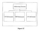
- FIG. 12shows the layout of a sensing array that uses CNT fabrics to detect IR and UV radiation
- FIG. 13Aillustrates an opto-isolator
- FIG. 13Billustrates a carbon nanotube opto-isolator according to one embodiment
- FIG. 14Ashows a simple circuit diagram of a temperature sensing circuit
- FIG. 14Bshows a graphical representation of the resistance and temperature ranges of thermistors and RTDs
- FIG. 15Adisplays a simple design of a CNT thermistor or RTD device
- FIG. 15Bis a FESEM image of a patterned CNT fabric that is interconnected with metal lines, which can be used as a CNT temperature sensor;
- FIG. 16Ais a cross-section of a suspended CNT thermistor
- FIG. 16Bshows an FESEM image of a suspended CNT fabric that would be used as a suspended CNT temperature sensor
- FIG. 17gives a representation of an array of CNT thermistor or RTD devices that would be used for various sensing applications
- FIG. 18Ashows a dye-sensitive photovoltaic cell
- FIG. 18Bshows dye-sensitive photovoltaic cell band diagram with carbon nanotubes as hole transport medium
- FIG. 18Cshows a band diagram of a dye-sensitive photovoltaic cell with a polymer blocking layer
- FIG. 19shows a possible design of a dye-sensitive photovoltaic cell with a CNT conducting matrix
- FIGS. 20A and 20Billustrate additional nanotube photovoltaic cell designs
- FIG. 21illustrates a nanotube photovoltaic cell impregnated with nanoparticles.
- Various embodiments of the inventionprovide carbon nanotube fabrics for use in electromagnetic radiation detecting and sensing systems and methods of making the same.
- Broad-range electromagnetic radiation sensors and detectorsmay be constructed with nanotube fabrics.
- Carbon nanotubeshave unique electrical and thermal properties that make them excellent materials for electromagnetic radiation and, specifically thermal detection.
- Fabrics constructed from carbon nanotubeshave the capability of sensing a wide spectrum of radiation, from Gamma Rays ( ⁇ 1 ⁇ ) to Radio Frequencies ( ⁇ >0.1 cm).
- CMOS technologyWith very low metal contamination levels, nanotube fabrics can be readily deposited on a variety of substrates and can be integrated with CMOS technology.
- the attributes of carbon nanotubes and carbon nanotube fabricsmake them an excellent and high-performance material when used in electromagnetic and thermal detectors.
- the performance advantages of detectorse.g. microbolometers constructed with carbon nanotube fabric are complemented by their versatility in detecting a broad range of the electromagnetic spectrum.
- Arrays of nanotube fabric detectorsmay be patterned on a single wafer, each individual detector in the array tuned to be sensitive to a predetermined range of electromagnetic radiation. Tuning the individual detectors may include functionalizing, derivatizing, doping portions of nanotube fabric (or using another suitable method) to sensitize the fabric to a selected range of the electromagnetic radiation spectrum.
- a broad-range detection arraymay be constructed to include detectors tuned to be sensitive to the UV range of the spectrum, detectors tuned to be sensitive to the IR range of the spectrum, and detectors tuned to detect intermediate ranges of the spectrum. Because the nanotube fabric detectors are readily fabricated and electrically connected with CMOS integration techniques, it is possible to deposit, pattern and interconnect the nanotube fabric detectors at any device level to measure radiation incident on and temperature fluctuations in an active device.
- detectors used for optical and optoelectronic applications in the semiconductor industryare typically micron-sized or larger structures and are discrete components that can only detect radiation of within a narrow spectrum.
- CMOS process flowfor integrated circuits.
- these detectorsshould also have the capability to detect a wide spectrum of radiation from Gamma Rays ( ⁇ 1 ⁇ ) to Radio Frequencies ( ⁇ >0.1 cm).
- Such sensing elementshave the potential for a broad range of usefulness in most types of consumer electronics where any electromagnetic detection in integrated circuits is beneficial. Solutions to the problems with current EM detectors are provided herein by employing carbon nanotubes, specifically carbon nanotube technology disclosed in the incorporated Nantero references.
- CNT detectorsthat sense EM radiation from UV to IR and other radiation events such as gamma, alpha or beta radiation either with a functionalized or non-functionalized fabric is described below.
- CNT fabricsfor the creation of microbolometers that surpass the ease of fabrication, operational characteristics and resolution obtainable with current VOx technology is detailed below.
- thermistorsand Resistive Temperature Detectors (RTDs), which employ the TCR of a material to detect temperature changes in a system.
- TTDResistive Temperature Detector
- the TCRis also very important for detection of EM with microbolometers.
- thermistorAs the temperature increases, the resistance of the thermistor decreases, hence negative TCR.
- RTDswhere an increase in temperature produces an increase in the resistance and a positive TCR of the detector.
- Table 1shows some TCR values of several materials that are typically used for either an RTD (positive TCR) or a thermistor (negative TCR).
- R refthe resistance of the material at T ref (typically at 20° C.).
- Thermistorsare more sensitive than the RTD devices, typically be a factor of 10, since RTDs have a much smaller TCR value; therefore, there is a smaller resistance change associated with RTD devices with modulating temperatures compared to thermistors.
- Germanium thermistorsare commonly used for temperatures ⁇ 100 K; while, silicon thermistors are used between 100-250 K. Above 250 K, the TCR of silicon becomes positive, which leads to a decrease in the resistance, potentially skewing temperature data. Since some semiconductors or metal oxide thermistor materials have large energy gaps, they are ideally suited for high temperature detection.
- Thermistorsalso typically have resistance values between 1 k ⁇ to 10 M ⁇ , while RTDs have resistance values ⁇ 1 ⁇ .
- Platinumis widely employed because it is a high melting point metal.
- the usable range for Pt RTDsis between ⁇ 200-630° C. with possible detection up to 900° C., with reduced accuracy.
- CNTshave unique electrical and thermal properties that also make them excellent candidates for temperature detection, along with EM detection.
- carbon nanotube fabrics that have a very low metal contamination level (low parts-per-billion)can be readily deposited onto a wide variety of substrates and can be integrated with CMOS technology are an ideal candidate for thermistor or RTD technology.
- Very low contamination levels of carbon nanotube fabricsare more fully described in U.S. patent application Ser. No. 10/860,332, the entire contents of which are herein incorporated by reference.
- CNT based thermistorshave many advantages over normal metal-oxide or single crystal semiconductor thermistors (or metal RTDs).
- One advantageis the ease of creating a CNT based thermistor (or RTD).
- CNT-thermistors (or RTDs)as with EM detectors, are readily fabricated using standard CMOS integration techniques such as spin-coating, optical lithography and Reactive Ion Etching (RIE), unlike current thermistor (or RTD) schemes, CMOS fabrication and integration techniques described in U.S. Pat. No. 6,706,402, U.S. patent application Ser. No. 10/341,005 and U.S. patent application Ser. No. 10/341,130, the entire contents of which are herein incorporated by reference.
- CNT thermistorsor RTDs
- substratessuch as flexible polymers, quartz, alumina, etc.
- CNT based thermistors and RTDscan also be fabricated with nanometer sized dimensions ( ⁇ 100 nm), which is not possible with current thermistor and RTD technology.
- CNT temperature sensorsare able to handle a much larger temperature range than their conventional counterparts.
- carbon nanotubesshould have a very wide sensing range because of their much larger melting point (>3000° C.) compared to RTD metals such as Pt (melting temperature: 1769° C.; range: ⁇ 200° C.-600° C.) or thermistor semiconductor materials such as Ge (melting temperature: 938° C. range: ⁇ 173° C.).
- CNT thermistorsare low power devices.
- the CNT thermistors or RTDshave minimal self-heating effects.
- the present disclosuredescribes techniques that enable the use of CNT fabrics for the detection of temperature changes within in a system, specifically for integrated circuit (IC) technology, nanoelectronics and lab-on-a-chip technology.
- the CNT thermistor/RTDmay be functionalized to tailor the TCR properties of the fabric; while in another aspect the combination of thermal detectors and heat detectors is shown.
- Fabrics of carbon nanotubesmay be either suspended over gaps (90-180 nm, e.g.) or conformal to a substrate could be employed as EM detectors. With moderate photon count, detection should be possible either by photo-generation (photodiode), fabric heating (bolometer) or phonon-generation (photo-acoustic).
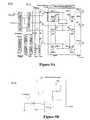
- FIG. 1Aillustrates an EM detecting element 100 constructed according to principles of certain embodiments of the invention.
- EM detecting element 100includes a nanotube ribbon 102 , a suspended region 106 of nanotube fabric, a gap region 110 , an insulating layer 108 comprising one or more supports 104 , electrodes 122 and driving circuitry 130 .
- the nanotube ribbon 102 of certain embodimentsis formed from a non-woven fabric of entangled or matted nanotubes (more below).
- Supports 104are patterned out of insulating layer 108 .
- Layer 108may be of any appropriate material, such as, but not limited to, SiO 2 , SiN x , HfO 2 , HfAlO, HfSiO, TiO 2 , Al 2 O 3 (crystalline and non-crystalline), MgO, Mylar, ZnO, BeO, fused-silica and other silica based insulators, plastics, porous membranes, and paper.
- EM detecting elementshave a suspended region 106 of nanofabric overlying a gap 110 , above a second substrate material 112 .
- Second substrate material 112may be an insulator such as one listed above and may be the same insulating material as 108 or second substrate material may be a semiconductor (such as, but not limited to, Si (single crystal, polycrystalline and amorphous), Ge, SiGe, SiC, Diamond, GaN, GaAs, GaP, AlGaAs, InP, GaP, CdTe, AlN, InAs, Al x In 1-x P, and other III-V and II-VI semiconductors) or a conductor (such as, but not limited to, Al, Cu, W, Al ( ⁇ 1% Cu), Co, Ti, Ta, W, Ni, Mo, Ru, Pd, Pt, Ag, Au, Au/Ti, Bi, Ca, Cr, Cr/Au, Fe, In, Mg, Na, Os, Pb, Rh, Sb, Sn,
- FIG. 1Billustrates an array 120 of detecting elements 100 .
- electrodes 122are connected by nanotube traces 112 and the array of suspended nanofabric regions 106 are each capable of acting as a detecting element 100 .
- FIG. 1Cillustrates a non-suspend EM detecting element 140 that is conformal to substrate 104 such as, but not limited to, silicon, SiO 2 , SiN x , GaAs, GaN, plastics, paper, etc.
- substrate 104such as, but not limited to, silicon, SiO 2 , SiN x , GaAs, GaN, plastics, paper, etc.
- This deviceis similar to FIG. 1A except that the carbon nanotube fabric detection area is not suspended.
- Non-suspended devicesare easier to fabricate; however, the substrate of a non-suspended device may adversely affect or skew the ability of the nanotube fabric to detect EM, by adsorbing a percentage of the EM radiation or perturbing the structure of the nanotubes, which, in turn, alters the properties of the nanotube fabric.
- a suspended fabricwill be more desirable, such as microbolometers where thermal isolation is important; however, other applications such as EM detection by exciton generation or through
- the substrate 104 in FIG. 1Cmay also be a reflective substrate in relation to the desired EM detection spectrum. Such reflective coatings are known in the art.
- FIG. 1Dillustrates and array 150 of non-suspended light detectors 124 .
- SWNT devicesmay be fabricated by spin coating, spray-coating, dip-coating or growing by CVD on a substrate as described in U.S. Pat. Nos. 6,706,402 and 6,835,591, as well as in U.S. patent application Ser. Nos. 10/341,054 and 10/341,130, the entire contents of which are herein incorporated by reference.
- the nanotube fabriccan then be patterned and electrically interconnected by using standard (photolithography) and non-standard (electron-beam or nanoimprint) lithography, etching (Reactive Ion Etching in oxygen) and metal deposition techniques (physical vapor deposition, chemical vapor deposition, electro-chemical deposition). Such fabrication is more fully described in the incorporated references.
- EM radiationcan be impinged on the open area of these SWNT fabrics to cause the generation of a photocurrent, such as a photodiode, the generation of heat in the fabric, such as a bolometer, or the generation of phonons in the fabric by the photo-acoustic effect.
- a photocurrentsuch as a photodiode
- the generation of heat in the fabricsuch as a bolometer
- the generation of phonons in the fabric by the photo-acoustic effectcan be impinged on the open area of these SWNT fabrics to cause the generation of a photocurrent, such as a photodiode, the generation of heat in the fabric, such as a bolometer, or the generation of phonons in the fabric by the photo-acoustic effect.
- Nanofabric ribbons or segments or belts made from a matted layer of nanotubes or a non-woven fabric of nanotubesare used as a conductive element which detect EM radiation.
- the ribbonsare referred to as traces or detecting or sensing articles or conductive articles.
- the ribbonsare suspended, and in other instances they are disposed conformally on a substrate.
- the sensing articlesmay be made from a nanotube fabric, layer, or film.
- SWNTs with tube diameters 0.5-4 nm or multi-walled nanotubes (MWNTs) with diameters >2 nmare electrical conductors that are able to carry extremely high current densities, see, e.g., Z. Yao, C. L. Kane, C. Dekker, Phys. Rev. Lett. 84, 2941 (2000). They also have the highest known thermal conductivity, see, e.g., S. Berber, Y.-K. Kwon, D. Tomanek, Phys. Rev. Lett.
- a trace made from nanotube fabriccreates its own electrical network of individual nanotubes within the defined trace, each of which may conduct electrons.
- current technologymay be used to create such traces.
- using a fabric of nanotubesalso increases the detection area/cross-section, allowing for much higher detection efficiencies compared to individual nanotubes.
- the CNT fabricconsists of a monolayer ( ⁇ 1 nm) up to a thick multilayer (>>10 nm) fabric.
- Multilayered fabricsmay be more suited for EM sensing. Multilayered fabrics will maximize the detection area of the nanotube detector, where as, monolayer fabrics, which may contain a porosity of 80-90%, will have a low detection efficiency due to the limited sensing surface area.
- a reflective substrate or thin filmcan be employed.
- the substratecan be tailored.
- a Copper, which reflects LWIR, substratecan be employed to reflect IR radiation back into the CNT fabric, increasing IR energy adsorption.
- suspended fabricscan also employ the benefits of a reflective substrate or thin film, in which a cavity is lined with a reflective medium (see microbolometers below).
- the nanotube fabricis used as a photodiode to detect EM radiation.
- FIG. 2shows detector element 200 , which generates photocurrent due to the recombination of electrons 235 and holes 236 .
- Nanotube detecting element 225is disposed onto substrate 210 and electrically contacted to source-drain electrodes 205 and 205 ′. The nanotube detector fabric is gated with gate electrode 215 separated from the nanotube fabric 225 by a thin dielectric 220 .
- the gating of the nanotube fabricallows for hole 236 generation from the drain region 205 ′ into the nanotube fabric 225 due to a small Schottky barrier.
- hole 236 generationfrom the drain region 205 ′ into the nanotube fabric 225 due to a small Schottky barrier.
- electrons 235are created in the nanotube fabric, which combine with holes 236 and generates current.
- This photodiode detectorcan also be fabricated with a suspended nanotube fabric, which is not shown in this invention.
- FIG. 3shows photo-acoustic detector 300 with disposed nanofabric detector 325 on substrate 320 with electrical contacts 305 and 305 ′.
- light 330impinges nanofabric 325 to produce phonons 335 .
- These phononswill in turn traverse the nanofabric and interact with electrodes 305 and 305 ′.
- the interaction between the generated phonons and electrodeswill either cause a generation of electrons in the electrodes which can be sensed as a current with appropriate sensing circuitry, not shown, or produce heating which will cause a resistance change in the electrodes that can be sensed with appropriate sensing circuitry, not shown.
- a suspended fabricmay be more ideal to prevent the loss of phonons to the substrate. It is expected that the EM radiation will generate optical phonons, which in turn, scatter to form either electrons or acoustic phonons. The acoustic phonons can readily be lost into the substrate and not contribute to the detecting signal; therefore, removal of the underlying substrate should greatly improve the sensing efficiency.
- the light detecting nanofabricis used as a bolometer.
- a circuit schematic 400 of a conventional bolometeris given in FIG. 4 , showing a Wheatstone Bridge structure.
- Input voltage 410is connected at one point between resistor 430 and 430 ′ and at a second point between resistor 430 ′′ and 440 .
- Resistors 430 , 430 ′ and 430 ′′are of known value.
- Resistor 440is the detector resistor which will vary depending on the impingement of electromagnetic radiation.
- the output voltage of the circuitis measured with voltmeter 420 .
- FIGS. 5A and 5BA simple nanofabric bolometer 500 is shown in FIGS. 5A and 5B . More advanced and realistic CNT bolometer designs and descriptions are presented further below.
- nanofabric detector 525is disposed onto substrate 520 and connected to interconnects 505 and 505 ′.
- FIG. 5Ano light is impinging on the nanofabric sensor, hence, no heating and EM detection is occurring.
- FIG. 5Blight 530 is impinging on nanofabric 525 causing heating and changing the resistance of nanofabric 525 to nanofabric 535 . This change in resistance can then be measured with appropriate sensing circuitry, not shown.
- All of the above embodimentscan have a functionalized nanotube fabric as shown in FIG. 6A , structure 600 .
- photoconductive nanoparticles or EM sensitive molecules 635are functionalized, doped, or adhered to nanofabric 625 to enhance the sensing properties of the nanofabric. Examples of nanoparticles and EM sensitive agents are given below.
- FIG. 6Bshows an FESEM micrograph of a sparse nanotube fabric that has been impregnated with silica nanoparticles. It is envisioned by the inventors that a wide variety of nanoparticles from conductors, to semiconductors and insulators can be attached to the nanotube fabric either during the synthesis of the nanotube solution, as described in U.S. Pat. No. 6,990,009, U.S. Pat. Publication Nos. 2005/0269553 and 2005/0058797 and U.S. patent application Ser. No. 10/860,331, the entire contents of which are hereby incorporated by reference, or during the fabrication of the detector by direct deposition of the nanoparticles.
- the CNT EM detectoris functionalized or doped with a photoconductive materials.
- a photoconductive materialwould be nanoparticles of GaN such as those produced by Kabra et al in “Gallium nitride nanoparticles for solar-blind detectors,” Proceedings of the Indian Academy of Science (Chemical Science), 115 (2003), 459-463. These additive photoconductive materials would enhance the range and efficiency of the nanofabric detectors. It would then be possible to use the nanoparticles to detect photons with energies in the UV and the nanofabric to detect energies in the IR range. Depending on the type of photoconductive nanoparticle, a wide range of light spectrum can be detected.
- nanoparticlescan consist of, but are not limited to, SiC, Si, Diamond, GaAs, GaP, AlGaAs, InP, GaP, CdTe, AlN, Ge, InAs, Al x In 1-x P, etc, which are typical semiconductor materials utilized for EM detection from UV to IR.
- an aspect of this inventionis the doping of nanotube fabrics with semiconducting nanoparticles that would be used to detect specific photon energies. As charge is generated in the nanoparticles, the charge is transferred to the CNT fabric, which in turn passes the charge to appropriate sensing circuitry.
- the EM sensorsmay detect gamma rays and other radiation particles, x-rays, visible light, infrared or radio waves, while in other embodiments, the sensor are multicolor—i.e. detect from gamma rays to IR.
- the nanofabricmay be functionalized, either non-covalently or covalently (e.g., by derivatization) so as to interact specifically with a particular radiation energy.
- the functionalization of nanotube fabrics for the production of an electrical change in the nanotube fabrichas been more fully described in U.S. Pat. Publication No. 2005/0053525, and will not be presented in further detail here, as the entire contents of this publication are herein incorporated by reference.
- Various embodimentsare understood to use the principle that charge transfer between carbon nanotubes and adsorbed molecules (which are altered by the absorption of EM radiation) changes the nanotube conductance, so as to provide novel nanosensor schemes.
- Sensors according to certain embodimentscan be used in a way that allows detection and measurement of differences in their conductance or other electrical properties before and after the functionalized nanotubes are exposed to radiation.
- the change in the sensor's electrical propertiesmay be measured in conjunction with a gating electrode, disposed below or adjacent to the nanotubes, via a field effect on the semiconducting nanotubes, see, e.g., P. Qi et al., “Toward Large Arrays of Multiplex Functionalized Carbon Nanotube Sensors for Highly Sensitive and Selective Molecular Detection,” Nano Lett ., vol. 3, no. 3, pp. 347-51 (2003).
- a sensorwith a suspended nanofabric structure.
- nanotube fabricsmay be used to sense X-rays by the functionalization of the film with a substance such as iohexyl (a non-ionic contrast agent that absorbs x-rays).
- a substancesuch as iohexyl (a non-ionic contrast agent that absorbs x-rays).
- the electrical perturbation in the nanotube fabriccan be measured either by a resistance change or by a capacitance change. Sensing changes in a nanotube fabric have been more fully described in U.S. Pat. Publication No. 2005/0053525.
- fluorodeoxyglucoseemployed as a radioactive tracer isotope in Positron Emission Tomography. It is theorized that by utilizing a gated nanotube fabric, the fluorodeoxyglucose is exposed to X-ray radiation and decays by emitting a positron. The emitted positron then interacts and annihilates with electrons in the gated nanotube fabric. The annihilation of electrons in the nanotube fabrics causes the flow of a current through the fabric that can be sensed with appropriate circuitry.
- Such sensor technologyis more fully described in U.S. Patent Publication Nos. 2005/0053525 and 2005/0065741, the entire contents of which are herein incorporated in their entirety.
- absorbing agentssuch as butyl methoxydibenzoylmethane (used for absorbing harmful UVA radiation in sunscreens) or radiopharmaceuticals such as, but not limited to, In111-Diethylene triamine pentaacetic acid, Technetium-99 compounds, etc.
- the inventorsalso envision the ability to combine the chemical sensing aspects of a nanotube fabric, as detailed in U.S. Pat. Publication Nos. 2005/0053525 and 2005/0065741, with the reactivity of specific molecules/compounds to radiation.
- a molecule that is chemically altered by the impingement of radiationcan be detected by the nanotube chemical sensor.
- the inventorstheorize that a normally undetected molecule is in suspension or in physical contact to the nanotube fabric. Upon exposure, the molecule physically changes so that it is now detectable by the nanotube chemical sensor, which will be registered by an electrical change in the fabric.
- nanotube EM detectorshave several important and unique features that are not available with existing technologies.
- arrays of these nanotube EM detectorscan be formed using patterning technology at minimum dimensions of the lithography node used, i.e. Giga-sized CNT fabric EM detector arrays can be fabricated at 180 nm or smaller critical dimension size.
- Such methodsare more fully described in incorporated references, e.g., U.S. Pat. Nos. 6,574,130, 6,643,165, 6,706,402, 6,784,028, 6,911,682, 6,919,592, and 6,924,538; and U.S. patent application Ser. Nos. 10/341,005, 10/341,055, 10/341,054, 10/341,130, and 10/776,059.
- Such nanofabric-based detector devicesscale directly with the lithographic ground rule used, i.e. 180 nm, 130 nm, 90 nm and 65 nm sized emitters can be produced.
- monolithic CMOS integration of these detector arrayscan be accomplished using the fabrication and integration of self-encapsulated electromechanical switching cavities as described in incorporated references.
- EM detection in these embedded arrayscan be individually controlled (turned on/off) by transistors or other types of switch technologies such as nanotube memory. This is the first demonstration of a manufacturable technology that can be integrated at a level of as few as one EM detector per transistor/memory cell. The combination of these features allows for the design and fabrication of high resolution EM detector arrays, specifically >640 ⁇ 480 resolution IRFPAs, that is currently not possible with current detector technology.
- Certain embodiments of the inventionallow integration at a level of one EM detector per transistor at the minimum dimension of a given lithography node or the integration of large arrays that are addressed by CMOS logic circuits.
- CMOS logic circuitsPreviously only discrete components, such as silicon p-n diodes or non-embedded microbolometers, could be used as EM detectors for optoelectronic circuits.
- Other types of detectorsrequire complex and difficult fabrication techniques such as flip-chip processes to integrate with silicon semiconductor technology. Because CNT EM sensors can be integrated to form VLSI arrays, thus enabling optical interconnects with one light detector per transistor (or waveguide, depending on function), the fabrication of ultra-dense optical circuits is possible.
- a certain embodiment of this inventionis the use of CNT fabrics as microbolometers, simple structure presented in 5 A and 5 B.
- VOx microbolometersmay be replaced with CNT microbolometers for IRFPAs with the ability to detect light in the IR but also possibly in the UV range (not possible with current microbolometer technology).
- the use of carbon nanotubes in a resistive microbolometer sensor with wide wavelength detectionis described below.
- CNTs in resistive microbolometer structureswill have a distinct advantage over VOx because for the first time multi-color UV/IRFPAs will be possible with one dimensional or two dimensional arrays on a silicon substrate.
- the fabrication of these CNT based arrayswill be possible because of the proven capability to processing CNTs in CMOS, SOI and Bipolar wafer processing facilities. Processing capabilities are more extensively described in U.S. patent application Ser. Nos. 10/860,332, 10/341,130, and other patents and applications incorporated by reference. As stated previously, this capability is due to purification of the CNTs and removal of any elements or contaminants that will prove detrimental to CMOS, SOI and Bipolar silicon wafer processes—as is well-known in the art and detailed in the incorporated references.
- the microbolometer structure that is sensitive in the UV/MWIR/LWIR bandsis adaptable to both one dimensional and two dimensional array designs.
- the basic VOx microbolometer structureis described in FIG. 7—taken from U.S. Pat. No. 5,450,053.
- silicon substrate 700is used as a base for the microbolometer and as a heat sink.
- the detecting element 701incorporates VOx absorbing element 702 and IR transparent dielectric layer 703 .
- IR transparent layer 703consists of highly doped SiN x that acts as a mechanical support for the cantilevered detecting element 701 and as a conducting medium to transport the signal to metal electrode 704 (listed as X-line in schematic).
- Etched cavity 705is used to thermally isolate detecting element 701 , allowing for the fabrication of un-cooled IR detectors.
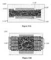
- FIG. 8shows a similar microbolometer structure as FIG. 7 ; however, the VOx adsorbing material is replaced with a CNT fabric.
- substrate and thermal sink 810has a fabricated detecting element 805 that consists of an IR absorbing nanotube layer 830 with IR transmitting silicon nitride layer 840 , cavity 850 , reflective coating 860 and metal electrode 820 . Note that only one electrical contact is shown in structure 800 and the metal electrode 820 can be connected directly to sensing circuitry or to underlying CMOS transistors.
- FIG. 8Bshows a similar microbolometer structure 801 ; however, instead of silicon nitride cantilever 840 , a ZnO cantilever structure 840 ′ is employed, which transmits UV radiation, and instead of IR reflector 860 , UV reflector 860 ′ is employed.
- CNT fabric 830is spin- or spray-coated on top of the 840 silicon nitride cantilever beam structure (IR detection) or 840 ′ ZnO cantilever structure (UV detection). Structures 830 , 840 and 840 ′ can readily be fabricated use CMOS photolithography and plasma etching techniques. CNT absorption has been demonstrated to be on the order of 70-80%, which coupled with the reflected radiation (described below) could increase the overall quantum efficiency of the microbolometer to over 90%, much greater than current VOx microbolometers.
- Cavity 850can readily be fabricated and has been previously described in incorporated references by employing a sacrificial layer.
- the sacrificial materialcan be amorphous or poly-silicon; however, any material that can be deposited, planarized and then wet, dry or vapor-phased etched with CMOS compatible processes can be employed.
- the cavity 850forms the cantilever beam structures that thermally isolate the microbolometer detecting region.
- Reflective coating 860 or 860 ′ on the bottom of the cavity 850reflects the radiation not absorbed by the first transmission through the CNT fabric.
- These reflective coatingscan be tuned for the multicolor response such as MWIR, LWIR or UV.
- MWIRMWIR
- LWIRlow-power optical characteristic
- Alaluminum
- UVultraviolet
- These reflective coatingsare known in the art and the inventors envision using reflective coatings depending on desired detection spectrum. A more detailed description of CNT fabric coatings and methods for providing them are included in U.S. Pat. Nos. 6,706,402 and 6,835,591.
- FIG. 8Cshows a top-down view 802 of structures 800 and 801 .
- the important aspects of the planar viewis that the nanotube fabric 830 can be either suspended freely with highly-doped silicon nitride clamp structures 840 or the nanotube fabric 830 can be deposited conformally on top of a highly doped silicon nitride plank.
- a gap 850 between the silicon nitride 840 and the nanotube fabric 830is shown for demonstration.
- the nanotube fabric 830would be connected to all the edges of the silicon nitride structure, similar to a picture frame.
- Metal electrode 820is connected to CMOS transistors or sensing circuitry that is not shown.
- the structures 800 and 801can be fabricated on the top of CMOS wafers with read out designs consisting of preamplifiers, integrators, sample and hold circuits and column multiplexer.
- the analog to digital converters, which are 14 bitcan either be integrated in the design or accomplished off chip.
- FIG. 9shows a possible circuit schematic of an entire CMOS embedded IR detector 900 device consisting of the CNT IR sensors ( 910 ), transistors, reference cells, and the CMOS Logic drivers, buffers and addressors.
- FIG. 9Bshows a schematic of the highlighted region 910 of CNT IR detector circuitry represented in FIG. 9A .
- This schematichas an additional capacitive trans-impedance amplifier for detector readout, which has been proven to increase the S/N ratio for VOx bolometers.
- the CNT detectorrepresented by the diode and which contains the CNT bolometer and attached transistors
- the preampis connected to the preamp at one input, while the second input is connected to a reference voltage.
- the output of the preampis attached to the digital logic circuits. Because of Nantero's CNT CMOS compatibility, similar circuitry as VOx bolometers can be designed for a CNT bolometer.
- IRFPAsThe dimensions of IRFPAs are optimized to minimize the 1/f noise of the microbolometer structure.
- SnowSee Snow, E. S. et al., “1/f noise in single-walled carbon nanotube devices”, Applied Physics Letters, Vol. 85, No. 18 (2004) 4172-4174
- NETDis inversely proportional to pixel size
- reducing the pixel size from 50 ⁇ m 2 to 15 ⁇ m 2will result in greater then 10 ⁇ improvement in NETD.
- Pixel sizes of 25 ⁇ m 2results in 640 ⁇ 480 pixel arrays. Therefore, pixel sizes of 15 ⁇ m 2 , which the inventors envision for CNT microbolometers) will result in 1280 ⁇ 960 pixel arrays with high fill factors and within the limits of chip sizes possible with current processing state of the art. Reducing for 25 ⁇ m 2 to 15 ⁇ m 2 sized pixel arrays will also minimize the cost of the optics, which is a major cost driver for these types of optical systems.
- the CNT micro-sensor presented in FIGS. 8A and 8Bis also a low mass sensor element that is thermally isolated from its environment. Previous work has shown that electrical power dissipated in the micro-sensor heats the CNT sensor element by an amount that is inversely proportional to the mass of the resistive element and thermal conductivity to the surrounding environment. The dissipated heat will flow to the surrounding structure with a time constant given by the thermal capacity times the thermal resistance to the surroundings. The response time will be on the order of 100 milliseconds while achieving sensitivity.
- the CNT microbolometerwill possibly be a high sensitivity detector because it meets the following requirements: high TCR, low 1/f noise, fast and operate under low power conditions, possibly have high sensitivity, can be deposited as a thin film ( ⁇ 100 nm), is compatible with CMOS, SOI and Bipolar processing, has a specific heat comparable to metals, and may have a film impedance compatible with readout circuitry requirements.
- Table 2compares the important parameters of an IR microbolometer between vanadium dioxide and a CNT fabric that Nantero would employ.
- FIG. 10shows another embodiment of this invention (structure 1000 ), where nanotube detecting fabric 1030 is not supported by mechanical support structure 840 as seen in FIG. 8A .
- nanotube fabric 1030is suspended over cavity 1050 , which is coated with reflective layer 1060 .
- EM detecting nanotube fabric 1030contacts electrodes 1020 and 1020 ′, which is embedded into insulating substrate 1010 .
- the suspending of a CNT fabricis this manner has been described in previous patents incorporated within and will not be discussed further here.
- One aspect of this designis that no IR transmitting highly doped silicon nitride or UV transmitting ZnO layer is required for structural support, thermal conduction and electrical conduction.
- metal electrodes 1020 and 1020 ′consist of a metal that has similar thermal conductivity as silicon nitride (30 W/m ⁇ K) or ZnO (130 W/m ⁇ K).
- silicon nitride30 W/m ⁇ K
- ZnO130 W/m ⁇ K
- titanium31 W/m ⁇ K
- Co100 W/m ⁇ K
- Ti and Coalso make good electrical contact to nanotube fabrics.
- Other conductorsmay also be employed which may appropriate thermal and electrical contact to the suspended EM detecting nanotube fabric.
- electrodes 1020 and 1020 ′consists of a Ti layer to make contact to the EM detecting nanotube fabric and the Ti is connected to a lower resistivity metal such as Al or Cu to make contact to the underlying interconnects, transistors, sensing circuitry, et cetera.
- FIG. 10Bshows another variation 1001 of an unsupported EM detecting nanotube.
- EM detecting nanotube fabric 1030is coated in either IR reflecting or IR transmitting layer 1060 ′ and 1060 ′′ and electrical contacts 1020 and 1020 ′.
- the coating layer 1060 ′ and 1060 ′′would consist of appropriate materials. For this example only IR will be discussed. If IR transmission to the electrodes is desired, then silicon nitride can be deposited and patterned over the CNT-metal contact area. This silicon nitride layer does not need to be highly doped for electrical conduction.
- a reflective layersuch as but not limited to Cu, can be deposited and patterned.
- layers 1060 ′ and 1060 ′′are IR reflecting materials such as Cu, which is also used for the reflector 1060 at the bottom of the cavity 1050 .
- FIG. 11Ashows a top view 1100 of structure 1000 shown in FIG. 10A .
- FIG. 11Bshows another top view structure 1100 related to structure 1000 of FIG. 10A where metal contacts 1120 and 1120 ′ are arrayed so that the exposed metal array is reduced, limiting any possible heating of the metal during exposure, which would contribute to background noise.
- FIG. 12shows a block diagram of a possible layout for a multi-bandwidth detector that has areas of the substrate dedicated for LWIR detection, while a second area focuses on MWIR detection and yet a third area is tailored for UV detection.
- the ability to fabricate a multi-colored detector arraycan be accomplished either through the tailoring of the integration process, i.e. such as using either silicon nitride or ZnO with the appropriate reflecting coatings or by functionalizing the nanotubes to absorb at different regions of the EM spectrum, as detailed above. With minimum feature sizes of ⁇ 250 nm and the CMOS compatibility, the inventors envision MBit arrays of EM detecting nanotube fabrics that cover the range of UV to IR.
- EM detecting nanofabricscan also be used as opto-isolators. Such an opto-isolator is useful in relay-type applications for isolating input to output.
- FIG. 13Aillustrates an LED and photodiode.
- the LED electrical input electrodes 1302 and 1304activate electrical input 1300 of LED 1312 sending a current through LED 1312 .
- LED 1312then generates an EM output signal 1314 .
- LED optical output signal 1314impinges on photodetector 1310 and photodetector 1310 generates output 1316 as a voltage between output electrodes 1306 and 1308
- FIG. 13Billustrates an opto-isolator according to one aspect of the invention where an EM detecting fabric is used as the photodetector.
- the LED electrical input electrodes 1302 ′ and 1304 ′activate electrical input 1300 ′ of LED element 1312 ′ sending a current through LED element 1312 ′.
- the spectrum of the EM outputcontains wavelengths in the infrared, visible, and ultraviolet regions of the spectrum, depending on the properties of the LED—i.e. the semiconductor material used for the LED.
- LED element 1312 ′ EM output 1314 ′impinges on a surface of a EM nanofabric detector 1310 ′.
- the nanofabric detectoris attached to 1306 ′ and 1308 ′.
- the EM nanofabric detectoroperates as a bolometer and generates output signal 1316 ′; however, the inventors also envision detecting EM energy through the generation of a photocurrent by electron-hole recombination or excitons, or by the generation of phonons that produce heating in electrodes 1306 ′ and 1308 ′ that in turn produces a resistance change.
- the nanofabric detectorscan also be attached to switching transistors or memory devices to create an optical switch, where the attached circuitry will not operate unless EM radiation is impinging on the nanotube detector fabric, to create a high conductive path for the case of exciton generation or a low conductive path for bolometers. This is more ideally suited for either the photodiode or photo-acoustic detector where current is generated due to the impinging EM energy.
- a major advantage of the nanotube nanofabric detectoris that an entire wafer may be filled with nanotube detectors and some or all of the detectors may be activated by a connected switch to create an optical switch.
- nanotube fabricUsed in conjunction with nanotube EM emitters, previously described in U.S. application Ser. No. 11/227,468, the entire contents of which are herein incorporated by reference, allows for optical circuits that employ nanotube EM emitting fabrics and nanotube EM sensing fabrics. This has many advantages in that the material used to create the light (nanotube fabric) will have the same optical properties (energy and wavelength) as the detector (nanotube fabric). With current optical technology, although silicon provides a reasonable detector material, silicon does not provide sufficient optical emission; therefore, other materials and techniques are required to generate light of sufficient wavelength that can be detected with silicon detectors. With the ease of fabrication of the nanotube emitters and detectors, nanotube fabrics are a reasonable replacement for current semiconductor emitters and detectors.
- nanotube fabric emitters and detectorsAnother advantage of the nanotube fabric emitters and detectors is that the same patterned fabric can be used for both an emitter and a detector. Therefore, with proper circuit design, the nanotube fabric can be used to emit EM radiation in one instance and detect EM radiation in another instance, minimizing used surface area on the substrate and minimizing fabrication costs and time.
- Nanotube detectorsintegrate well with silicon and other types of optical integration techniques, such as those used for group III-V and II-VI semiconductor technologies that are CMOS, SOI and Bipolar compatible. Nantero has demonstrated the patterning of nanotube fabrics on the CMOS sensitive p-type GaN material in, for example, U.S. Pat. Appl. No. 60/775,461, the entire contents of which are herein incorporated by reference.
- the EM detecting nanotube articleis made with single-walled carbon nanotubes; however, MWNTs or a mix of SWNTs and MWNTs can be used.
- MWNTs or a mix of SWNTs and MWNTscan be used.
- semiconducting nanotube speciesare certain.
- heat generation or phonon generationboth metal and semiconducting nanotubes may be used.
- Typical EM detecting nanotube fabric articleshave a width of 50 nm up to several microns and thicknesses of ⁇ 1 nm and >>10 nm.
- a typical suspension lengthis 50 nm up to 1 micron.
- the type of drive circuitrywill be application dependent.
- the circuitrymay be selected to ensure that sufficient voltage is provided to detect EM energy of an intensity and duration desired in a particular context.
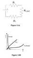
- FIG. 14AA circuit schematic of a simple conventional thermistor is given in FIG. 14A .
- R 1is the resistance of interconnect lines, while R Load is the resistance of the thermistor.
- R 1is a known resistance value and R Load has a variable resistance with a known value at room temperature.
- the thermistor materialcan be connected to a 4-terminal device or a bridge circuit. The same analysis can be applied to RTD technology.
- FIG. 14Bshows a graphical plot of the expected resistance and temperature ranges for thermistors and RTD devices.
- This embodimentdiscloses a route for nano-sized thermistors and RTDs structures that are based on CNT technology that may be used for discrete temperature sensing in a wide range of electronic and nanoelectronic applications.
- FIG. 15Ashows a design of a CNT thermistor (or RTD). The fabrication of such a thermistor is similar to the bolometer described above and has been described in references incorporated within.
- Structure 1500shows the insulating substrate, which can be formed by an insulator material such as, but not limited to SiO 2 and any silica based derivative, alumina, sapphire, Mylar, plastics and other flexible substrates.
- Area 1540Located on or within substrate 1510 of structure 1500 is an area 1540 , which is the location on the substrate where a temperature needs to be measured.
- Area 1540may be a resistor or conductor (such as a metal interconnect line in an integrated circuit), semiconductor (such as the transistor in CMOS Logic) or insulator (such as the gate oxide or interlayer dielectrics in a SRAM memory device) and structure 1540 may increase or decrease in temperature.
- thermally detecting nanotube fabric 1530In physical contact with thermally active area 1540 is thermally detecting nanotube fabric 1530 .
- semiconducting nanotubes or a semiconducting fabricshould be employed for the CNT thermistor, giving a negative TCR for the CNT fabric.
- Several methods exist and are known in the art for the separation of metallic nanotubes from semiconducting nanotubessuch as those detailed in U.S. patent application Ser. Nos. 10/341,005 and 10/341,130.
- the separation of the metallic nanotubes from semiconducting nanotubesmay be performed before the creation of an electronic grade CNT solution (see U.S. patent application Ser. No.
- thermally sensing fabric 1530is electrical isolated from 1540 ; therefore, if 1540 is an electrical conductor, than an insulating layer (not shown) such as a thin silicon oxide or silicon nitride can be deposited in between thermally active region 1540 and thermally sensing fabric 1530 . Ideally, such insulating layer should have a high thermal conductivity so that the heat can be transported to the thermally sensing nanotube fabric.
- the thermally detecting nanotube fabricis connected to metal electrodes 1520 and 1520 ′. These metal electrodes connect to appropriate sensing circuitry.
- Metal interconnects 1520 and 1520 ′are conductors such as, but not limited to, Ru, Ti, Cr, Al, Au, Pd, Ni, W, Cu, Mo, Ag, In, Ir, Pb, Sn, as well as other suitable metals, and metal alloys such as TiAu, TiCu, TiPd, PbIn, and TiW, or conductive nitrides, oxides, or silicides such as RuN, RuO, TiN, TaN, CoSi x and TiSi x .
- Pd and Tiare ideal contact metals because of the matching of the metal's work function to the vacuum energy of the CNTs, giving a nearly ohmic contact.
- Structure 1501 of FIG. 15Bshows an FESEM image of the representative structure that was fabricated in FIG. 15A .
- FIG. 15 BEshows substrate 1510 with patterned nanotube fabric 21530 and metal contacts 1520 and 1520 ′. Thermally active area 1530 from FIG. 15A would be deposed underneath or on top of CNT fabric 1530 .
- CNT thermistor(and another embodiment) is that the temperature detector is completely CMOS compatible, allowing for the fabrication of an on-chip temperature sensor, which can be used as a lab-on-a-chip.
- the resistance of the CNT-thermistorcan also be tailored from several hundred Ohms up to several Mega-Ohms.
- the CNT fabric used for the thermistorcan also be doped and functionalized to tailor the thermal and electrical properties of the fabric, specifically the TCR value of the nanotube fabric to adjust the detection range and temperatures.
- FIG. 16Ashows a similar thermistor design as FIG. 15A with substrate 1610 , temperature gradient source 1640 , nanotube thermistor fabric 1630 and metal interconnects 31620 and 1620 ′.
- structure 1600has a gap region 1670 that separates nanotube fabric 1630 from the area where the temperature needs to be measured 1640 .
- the gap region 1670may have a height of 1 nm up to several hundred nanometers and a length (width) of 10-10,000 nm.
- An advantage of a suspended CNT thermistoris that all of the heat (or temperature change) from the source is directed into the nanotube fabric and there is no loss of heat to the surrounding substrate. Another advantage is that there is no electrical contact between the suspended nanotube thermistor fabric 15300 and the heat source 1640 . This is important if the heat source is either a metallic interconnect or the active region of a CMOS transistor were the nanotubes may allow for a considerable amount of electrical leakage.
- FIG. 16Bshows FESEM image 1601 that has a nanotube fabric 1630 with a suspended nanotube fabric region 1630 ′ over a trench 1670 .
- FIG. 17shows structure 1700 , which represents an array of thermistors over a temperature source 1740 which is on substrate 1710 .
- thermal sensing nanotube fabric 1730is patterned into an array structure.
- the nanotube thermistorsare interconnected by metal lines 1720 and 1720 ′.
- the nanotube patternsmay have the same dimensions (i.e. length and width).
- the CNT thermistorscan by employed to measure of the temperature of the source changes along the length of the source.
- the thermistorswould be placed at separate locations along an interconnect line typically used for ICs.
- the CNT thermistorswould then be used to measure the variation in temperature of the interconnect line as current flows through the interconnect line and causes heating in the interconnect line by Joule heating. Using an array of CNT thermistors also gives redundancy to the CNT thermistor measurements, improving reliability.
- the CNT thermistorsmay have varying lengths and widths within the array (not shown).
- the reference resistance of the CNT thermistorwill be varied with increasing resistance as patterned CNT length increases and patterned CNT width decreases.
- the thermal detecting nanotube devicesmay also be disposed in a vertical orientation, as described in U.S. Pat. No. 6,924,538.
- the CNT fabricconsists primarily of metallic nanotubes and is metallic in nature, meaning that as the temperature increases the resistance of the fabric increases.
- This type of metallic nanotube fabricallows for the creation of a CNT-RTD device.
- the fabrication of the CNT-RTD deviceis the same as the thermistor device shown in FIG. 15 .
- the RTD deviceshave a positive coefficient of resistance (PTC).
- PTCpositive coefficient of resistance
- the advantage of a CNT RTDis that the CNT RTD should be able to handle a much larger temperature range compared to Pt (range ⁇ 200° C.-600° C.) due to the much higher melting point of carbon nanotubes (>3000° C.) compared to all metals.
- both a semiconducting CNT thermistor type fabric and a metallic CNT RTD type fabricare used in conjunction on the same device to give a wide range for the temperature detection. Since the semiconducting CNTs possess a relatively small band gap, the thermistors are more ideally suited for low temperature detection, while the metallic nanotubes can handle very high temperature detection because of the nanotubes high melting temperature.
- CNT thermistorscan be envisioned.
- the first application for a CNT thermistoris for on-chip temperature sensing and control for CMOS and SOI integrated circuits. Because the CNT thermistor is readily fabricated and electrically connected with CMOS integration techniques, it is possible to deposit, pattern and interconnect the CNT thermistors at any device level to measure the temperature of the active region at that level and then control the input parameters of the active area to control the amount of heating or cooling in the active device.
- the CNT thermistorwhich has a negative TCR, can be employed in conjunction with a metal resistor or interconnect to cancel out the positive temperature coefficient of the metal line.
- An advantage with the CNT thermistoris that the properties of the CNT fabric can be tailored to match the properties of the metal interconnect so that the decrease in resistance of the nanotube fabric can closely match the increase in resistance of the metal line; therefore, giving a near zero change in resistance of the entire system.
- CNT thermistoras a thermal relay and switch. This type of device is useful for power supply circuits, where the CNT fabric has a high resistance initially, preventing the flow of large currents when the device is turned to the ON state. Then as the system heats up and the resistance of the CNT thermistor decreases current is allowed to pass through the CNT thermistor, permitting for normal circuit operation.
- the CNT thermistorscan also be utilized for monitoring the rate of change in temperature and other parameters of the surroundings, such as liquid levels, fluid flow and vacuum level. This is not possible with standard thermal detectors, because the detector material may be reactive to the liquid matrix, whereas, the CNT fabric may be derivatized to alter its properties, especially sensitivity to liquids and/or hydrophobicity or hydrophilicity. These properties are more fully described U.S. Patent Publication Nos. 2005/0053525 and 2005/0065741.
- a nanotube detecting fabriccan be used in as a replacement for liquid electrolytes for dye-sensitized solar cells.
- Current dye-sensitized solar cellsuse dye-sensitized TiO 2 or other semiconducting nanoparticles mixed with a liquid electrolyte or an organic material to produce a photovoltaic signal (see Gratze, M “Photoelectrochemical cells”, Nature 414 (2001) 338-344 and U. Bach, et al, “Solid-state dye-sensitized mesoporous TiO 2 solar cells with high photon-to-electron conversion efficiencies”, Nature 395 (1998) 583-585).
- This inventionis related to detectors because EM radiation such as light energy from the sun is detected with the solar cell and then converted into usable energy for various applications.
- FIG. 18Ashows an energy band schematic of a dye-sensitized electrolytic solar cell.
- the energy band schematiccomprises anode ( 1802 ), TiO 2 ( 1804 ), dye-sensitive material ( 1806 ), electrolyte ( 1808 ), and cathode ( 1810 ).
- Solar energy (h ⁇ )interacts with the dye-sensitive material ( 1806 ), causing the excitation of an electron, which in turn transfers to the conduction band (low energy state) in the TiO 2 nanoparticle.
- the electronsmove through the nanoparticle network to a conducting anode ( 1802 ).
- the dye-sensitive material ( 1806 )is now at an oxidized state with a positive charge.
- a liquid electrolyte ( 1808 ) or an organic polymer phaseacts as the hole transport medium and serves to regenerate missing electrons in the dye and transport positive charges to the cathode ( 1810 ).
- the electronarises by a redox reaction, creating an electron for the dye and a hole for the cathode ( 1810 ); while, in organic-inorganic bulk hetero-junction solar cells an inorganic p-type semiconductor material or an organic charge transport material serves as hole conductors, replacing the electrolyte medium.
- Charge transport in hybrid organic-inorganic solar cellsis limited by percolation due to low connectivity networks. This prevents the charge carriers from reaching the electrodes before they can recombine and decrease the power conversion efficiency.
- highly conducting percolating networks and filmscan be fabricated with carbon nanotube fabrics; therefore, the use of carbon nanotube networks in place of organic/polymeric phases can overcome the percolation limited charge transport in hybrid organic-inorganic solar cells.
- FIG. 18Bshows an expected band profile of a dye sensitized solar cell with a SWNT fabric ( 1812 ) as the hole transport medium. The bands match very well for efficient hole (h + ) injection from the sensitizer to the nanotube network and subsequent transport through the nanotube network to the contact.
- Networks or films of single-walled, double-walled or multi-walled carbon nanotubescan be used ( 1812 ).
- the valence band edgemay vary from 4.5-5.0 eV, depending on the type of nanotubes used.
- the dye usedcan be a Ru based dye, which is used in standard dye-sensitiized solar cell.
- Carbon nanotubeshave an advantage over other mediums in that nanotube networks and films have hole mobilities of 1 cm 2 /Vs, which is several orders of magnitude higher than hole mobility of most of the organic or polymeric hole transport medium used in dye-sensitized and bulk hetero-junction solar cells (typical hole mobility is in the range of 1 ⁇ 10 ⁇ 1 to 1 ⁇ 10 ⁇ 3 cm 2 /Vs). Incorporating nanofabrics as the hole transport layer should lead to faster charge transport and higher efficiency solar cells. In addition to their high hole mobility, nanotube networks can be fabricated in the form of highly conducting films and fabrics due to their high aspect ratio and high intrinsic conductivity. Therefore, slow charge transport due to non-percolating networks that is common in organic-inorganic hybrid solar cells can be overcome by incorporating nanotube network as one of the charge transport phases.
- yet another embodimentuses the nanotube fabric as a photovoltaic solar cell in conjunction with dye-sensitized nanoparticles.
- the nanotube fabricis not acting as a detecting medium, the entire device is used to detect and convert energy into power.
- Nanotube films and networksmay be used as a medium for hole (or positive charge) transport in dye-sensitized solar cells.
- the correct contact metal to the nanotube fabricis required.
- Studies such as those done by Z. Chen, et al (“The role of metal-nanotube contact in the performance of carbon nanotube transistors”, Nano Letters, 5(7) (2005) 1497-1502)have shown that most metals form a Schottky barrier contact with p-type characteristics to semiconducting nanotubes, meaning that the contacts inject holes into the semiconducting nanotubes.
- Y. Chen, et al(“The role of metal-nanotube contact in the performance of carbon nanotube transistors”, Nano Letters, 5(7) (2005) 1497-1502) have shown that most metals form a Schottky barrier contact with p-type characteristics to semiconducting nanotubes, meaning that the contacts inject holes into the semiconducting nanotubes.
- Using a p-type connection on one end of the nanotubes (hole injection from dye into nanotube fabric) and n-type connection on the other end of the nanotube fabric (electron injection from Ca or Al contact into nanotube fabric)allows for the realization of using the nanotube fabric as a hole transport medium in dye-sensitized solar cells.
- FIG. 18Cshows the band profile a dye sensitized solar cell with nanotubes as the hole transport layer and a polymeric interlayer to block possible electron transfer from the dye molecule to the nanotubes.
- Poly-3-octyl thiophene (P3OT) or other polymers ( 1814 ) with an appropriately matched energy level with respect to the dye and the nanotubes (e.g. single-walled nanotubes) ( 1812 )can be used as the blocking layer.
- the dye usedis N-(1-pyrenyl)maleimide dye for better energy level matching with the P3OT ( 1814 ) blocking layer.
- Homogeneous nano-scale mixing of the CNT and the nanoparticle phasescan be achieved by using nanotube networks and films functionalized with the desired inorganic nanoparticles as described above.
- Nano-scale mixing of the phasescan also be achieved through layer-by-layer deposition of alternating nanotube and nanoparticle networks.
- Layer-by-layer depositioncan be done by coating alternate layers of carbon nanotube and nanoparticles.
- Dispersions of commercially available TiO 2 nanoparticles ( 1804 )can be used to apply the nanoparticle layer.
- the layers/filmscan be applied either by spin or spray coating as described in incorporated references.
- FIG. 19shows a schematic of a solar cell structure 1900 made from carbon nanotubes, TiO 2 , and dye molecules.
- the cellcomprises of a insulating substrate 1910 coated with a fluorinated tin oxide (SnO:F) or indium tin oxide (ITO) layer 1970 .
- the SnO:F or the ITO layerforms a transparent bottom electrode through which the light strikes the active layer.
- a smooth TiO 2 film 1950which supports the nanoparticles and prevents shorting of the nanotubes in the active layer to the bottom electrode 1960 .
- the active layer 1940Above the smooth TiO 2 layer is the active layer 1940 , which in this particular example is a dye sensitized TiO 2 nanoparticle network impregnated on a nanotube network.
- a nanotube overlayer 1930which provides good electrical contact to the top electrode 1920 .
- the top electrode 1920is any metal that gives a n-type connection to the nanotube fabric, such as but not limited to Al and Ca.
- FIG. 20Ashows another possible design for a dye-sensitized photovoltaic cell 2000 with a nanotube fabric hole transport medium 2025 deposed onto insulator 2020 .
- nanofabric 2025is contacted on one end with dye material 2035 and semiconducting nanoparticle matrix 2015 .
- the nanoparticle matrixis attached to a conducting electrode 2005 .
- the other end of the nanofabric 2025is contact to n-type contact metal 2045 which in turn is contact to metal electrode 2005 ′.
- Electrodes 2005 and 2005 ′may be constructed from a wide variety of metals such as, but not limited to Al, Cu, W, Al ( ⁇ 1% Cu), Co, Ti, Ta, W, Ni, Mo, Pd, Pt, TiW, Ru, CoSi x , WSi 2 , TiSi x , TaN, TiN, TiAlN, RuN, RuO, PtSi, Pd 2 Si, MoSi 2 , NiSi x , Ag, Au, Au/Ti, Bi, Ca, Cr, Cr/Au, Fe, In, Ir, Mg, Na, Ni, NiSi 2 , Os, Pb, Rh, RhSi, Sb, Sn, Pb/Sn, PbIn, Zn and ZrSi 2 .
- metalssuch as, but not limited to Al, Cu, W, Al ( ⁇ 1% Cu), Co, Ti, Ta, W, Ni, Mo, Pd, Pt, TiW, Ru, CoSi x , WSi
- FIG. 20Alight of energy h ⁇ impinges on the dye material 2035 , which transfers an electron to the semiconducting nanoparticle matrix 2015 and a hole to nanotube fabric 2025 .
- the electronis then transferred to the conducting electrode 2005 , while, the hole is transferred along the nanotube fabric 2025 to contact electrode 2045 .
- the electrodes 2005 and 2005 ′are connected to corresponding circuitry (not shown) that is used to collect the excess electron energy.
- FIG. 20Bshows yet another design of the above embodiment where nanotube fabric 2025 is disposed on top of dye material 2035 and nanoparticle material 2015 . Since nanofabric 2025 is highly porous, light of energy h ⁇ can freely interact with dye material 2035 , with a minimal loss in photon energy to the fabric.
- FIG. 21shows a schematic of this device where nanoparticles 2115 and dye material 2135 is incorporated within fabric 2125 .
- These nanotube hole transfer mediumsmay also be constructed from multi-walled and double-walled carbon nanotubes and also may be formed into monolayer of multilayered fabrics as long as the fabric maintains semiconductor characteristics.
- in an alternate embodiment of the inventionis to use nanowires or nanotubes of TiO 2 or ZnO in place of nanoparticles to make dye-sensitized solar cells with carbon nanotubes.
- the CNT fabricis primarily employed as a charge carrier transport medium, it is also possible for the CNT fabric to also assist in the detection/collection of photon energy by the same detector properties that were described above.
Landscapes
- Physics & Mathematics (AREA)
- General Physics & Mathematics (AREA)
- Spectroscopy & Molecular Physics (AREA)
- Health & Medical Sciences (AREA)
- Life Sciences & Earth Sciences (AREA)
- High Energy & Nuclear Physics (AREA)
- Molecular Biology (AREA)
- Chemical & Material Sciences (AREA)
- Engineering & Computer Science (AREA)
- Nanotechnology (AREA)
- Photometry And Measurement Of Optical Pulse Characteristics (AREA)
Abstract
Description
| TABLE 1 |
| TCR values for several materials that can |
| be used as either RTDs or thermistors. |
| Material | TCR (° C. − 1) | ||
| Al | 0.0041-0.004308 | ||
| Au | 0.003715-0.004 | ||
| Pd | 0.00377 | ||
| Pt | 0.003729-0.003927 | ||
| Si | −0.07 | ||
| Ge | −0.05 | ||
where a, b and c are Steinhart parameters. Thermistors are more sensitive than the RTD devices, typically be a factor of 10, since RTDs have a much smaller TCR value; therefore, there is a smaller resistance change associated with RTD devices with modulating temperatures compared to thermistors. Germanium thermistors are commonly used for temperatures ≦100 K; while, silicon thermistors are used between 100-250 K. Above 250 K, the TCR of silicon becomes positive, which leads to a decrease in the resistance, potentially skewing temperature data. Since some semiconductors or metal oxide thermistor materials have large energy gaps, they are ideally suited for high temperature detection. Thermistors also typically have resistance values between 1 k□ to 10 M□, while RTDs have resistance values <1 □.
| Key Microbolometer | Reasons for | ||
| Parameters | Vanadium Oxide | Carbon Nanotubes | CNT advantage |
| Responsivity/Signal to noise | 500:1 | ≧500:1 | |
| ratio | |||
| NETD @300K 30 Hz f/1 | 20 mK | ≦20 mK | Noise levels |
| Optics | equiv to VOx | ||
| could be | |||
| improved | |||
| Resolution: Scale as the | 640 × 480 | Same-scalable to | Resolution is |
| CMOS processing capability | @25 micron cell size | 1280 × 960 | possible in both |
| scale | technologies | ||
| TCR | 1-2.5%: −0.023 (K−1) | Potential for better | Single layer |
| positive TCR ,anneal | CNT films | ||
| out metallic CNT | Only semi | ||
| CNT | |||
| 100 mSec | same | ||
| Fill Factor | >80% | same | |
| Pixel Operability | >99% | same | |
| Compatibility with CMOS | Yes | same | |
| Spectral response: UV | 8-12 microns | UV through 12 | Absorption |
| through LWIR | 80% Absorption | Microns, maybe | coefficient 104 |
| beyond- | to 105cm−1 | ||
| MWIR/LWIR | Ability to | ||
| possible | functionalize | ||
| 80% absorption with | |||
| cavity reflecting | |||
| layer | |||
- U.S. patent application Ser. No. 10/341,005, filed on Jan. 13, 2003, entitled Methods of Making Carbon Nanotube Films, Layers, Fabrics, Ribbons, Elements and Articles;
- U.S. patent application Ser. No. 09/915,093, now U.S. Pat. No. 6,919,592, filed on Jul. 25, 2001, entitled Electromechanical Memory Array Using Nanotube Ribbons and Method for Making Same;
- U.S. patent application Ser. No. 10/033,032, now U.S. Pat. No. 6,784,028, filed on Dec. 28, 2001, entitled Methods of Making Electromechanical Three-Trace Junction Devices;
- U.S. patent application Ser. No. 10/033,323, now U.S. Pat. No. 6,911,682, filed on Dec. 28, 2001, entitled Electromechanical Three-Trace Junction Devices;
- U.S. patent application Ser. No. 10/128,117, now U.S. Pat. No. 6,835,591, filed on Apr. 23, 2002, entitled Methods of NT Films and Articles;
- U.S. patent application Ser. No. 10/844,913, now U.S. Pat. Publ. No. 2005/0053525 filed on May 12, 2004, entitled Horizontally Oriented Sensor Constructed with Nanotube Technology;
- U.S. patent application Ser. No. 10/844,883, now U.S. Pat. Publ. No. 2005/0065741, filed on May 12, 2004, entitled Vertically Oriented Sensor Constructed with Nanotube Technology;
- U.S. patent application Ser. No. 10/341,055, filed Jan. 13, 2003, entitled Methods of Using Thin Metal Layers to Make Carbon Nanotube Films, Layers, Fabrics, Ribbons, Elements and Articles;
- U.S. patent application Ser. No. 10/341,054, filed Jan. 13, 2003, entitled Methods of Using Pre-formed Nanotubes to Make Carbon Nanotube Films, Layers, Fabrics, Ribbons, Elements and Articles;
- U.S. patent application Ser. No. 10/341,130, filed Jan. 13, 2003, entitled Carbon Nanotube Films, Layers, Fabrics, Ribbons, Elements and Articles;
- U.S. patent application Ser. No. 10/776,059, now U.S. Publication No. 2004/0181630, filed Feb. 11, 2004, entitled Devices Having Horizontally-Disposed Nanofabric Articles and Methods of Making The Same;
- U.S. patent application Ser. No. 10/776,572, now U.S. Pat. No. 6,924,538, filed Feb. 11, 2004, entitled Devices Having Vertically-Disposed Nanofabric Articles and Methods of Making the Same;
- U.S. patent application Ser. No. 10/128,118, now U.S. Pat. No. 6,706,402, filed Apr. 23, 2002, entitled Nanotube Films and Articles;
- U.S. patent application Ser. No. 09/915,173, now U.S. Pat. No. 6,643,165, filed Jul. 25, 2001, entitled Electromechanical Memory Having Cell Selection Circuitry Constructed with Nanotube Technology;
- U.S. patent application Ser. No. 09/915,095, now U.S. Pat. No. 6,574,130, filed Jul. 25, 2001, entitled Hybrid Circuit Having Nanotube Electromechanical Memory;
- U.S. patent application Ser. No. 10/918,085, now U.S. Pat. No. 6,990,009, filed Aug. 13, 2004, entitled Nanotube Based Switching Elements with Multiple Controls;
- U.S. patent application Ser. No. 10/860,432, now U.S. Pat. Publication No. 2005/0269553, filed Jun. 3, 2004, entitled Spincoatable Liquid for Use in Electronic Fabrication Processes;
- U.S. patent application Ser. No. 10/860,332, now U.S. Pat. Publication No. 2005/0058797, filed Jun. 3, 2004, entitled High Purity Nanotube Fabrics and Films;
- U.S. patent application Ser. No. 10/860,331, filed Jun. 3, 2004, entitled Method of Making an Applicator Liquid for Electronics Fabrication Process;
- U.S. patent application Ser. No. 10/844,913, now U.S. Pat. Publication No. 2005/0053525, filed May 12, 2004, entitled Sensor Platform Using a Horizontally Oriented Nanotube Element;
- U.S. patent application Ser. No. 11/227,468, filed Sep. 15, 2005, entitled Light Emitters using Nanotubes and Methods of Making Same; and
- U.S. Provisional Pat. Apl., No. 60/775,461, filed Feb. 21, 2004, entitled Method of Forming Carbon Nanotube Based Contact to Semiconductor.
Claims (14)
Priority Applications (1)
| Application Number | Priority Date | Filing Date | Title |
|---|---|---|---|
| US12/046,855US8110883B2 (en) | 2007-03-12 | 2008-03-12 | Electromagnetic and thermal sensors using carbon nanotubes and methods of making same |
Applications Claiming Priority (2)
| Application Number | Priority Date | Filing Date | Title |
|---|---|---|---|
| US90640907P | 2007-03-12 | 2007-03-12 | |
| US12/046,855US8110883B2 (en) | 2007-03-12 | 2008-03-12 | Electromagnetic and thermal sensors using carbon nanotubes and methods of making same |
Publications (2)
| Publication Number | Publication Date |
|---|---|
| US20080251723A1 US20080251723A1 (en) | 2008-10-16 |
| US8110883B2true US8110883B2 (en) | 2012-02-07 |
Family
ID=39759992
Family Applications (1)
| Application Number | Title | Priority Date | Filing Date |
|---|---|---|---|
| US12/046,855Active2029-04-25US8110883B2 (en) | 2007-03-12 | 2008-03-12 | Electromagnetic and thermal sensors using carbon nanotubes and methods of making same |
Country Status (3)
| Country | Link |
|---|---|
| US (1) | US8110883B2 (en) |
| TW (1) | TWI475673B (en) |
| WO (1) | WO2008112764A1 (en) |
Cited By (30)
| Publication number | Priority date | Publication date | Assignee | Title |
|---|---|---|---|---|
| US20100308848A1 (en)* | 2009-06-03 | 2010-12-09 | Kaul Anupama B | Methods for gas sensing with single-walled carbon nanotubes |
| US20110051775A1 (en)* | 2009-08-26 | 2011-03-03 | Ut-Battelle, Llc | Carbon nanotube temperature and pressure sensors |
| US20110316113A1 (en)* | 2010-06-28 | 2011-12-29 | Seiko Epson Corporation | Pyroelectric detector, pyroelectric detection device, and electronic instrument |
| US20110315882A1 (en)* | 2010-06-25 | 2011-12-29 | Hon Hai Precision Industry Co., Ltd. | Infrared detector |
| US20130048884A1 (en)* | 2011-07-08 | 2013-02-28 | The Johns Hopkins University | Agile ir scene projector |
| US20130107344A1 (en)* | 2011-10-31 | 2013-05-02 | International Business Machines Corporation | Optoelectronic device employing a microcavity including a two-dimensional carbon lattice structure |
| US20130122690A1 (en)* | 2011-11-10 | 2013-05-16 | Huilong Zhu | Method for removing metallic nanotube |
| US20130327960A1 (en)* | 2012-06-12 | 2013-12-12 | Jun Zhu | System for measuring light intensity distribution |
| US20140264700A1 (en)* | 2013-03-13 | 2014-09-18 | The Aerospace Corporation | Monolithic sun sensors, assemblies thereof, and methods of making and using same |
| US20140335650A1 (en)* | 2013-05-10 | 2014-11-13 | International Business Machines Corporation | Graphene photodetector |
| WO2015109410A1 (en)* | 2014-01-23 | 2015-07-30 | The Governors Of The University Of Alberta | Chemical sensor |
| US20150349184A1 (en)* | 2014-05-30 | 2015-12-03 | Klaus Y.J. Hsu | Photosensing device with graphene |
| US20150349185A1 (en)* | 2014-05-30 | 2015-12-03 | Klaus Y.J. Hsu | Photosensing device with graphene |
| RU2595306C1 (en)* | 2015-07-03 | 2016-08-27 | Общество с ограниченной ответственностью "Фотоэлектронные приборы" | Heat radiation sensor and its manufacturing method |
| US9435896B2 (en) | 2013-07-31 | 2016-09-06 | Globalfoundries Inc. | Radiation detector based on charged self-assembled monolayers on nanowire devices |
| US20170117312A1 (en)* | 2015-10-21 | 2017-04-27 | Massachusetts Institute Of Technology | Nanowire fet imaging system and related techniques |
| US20170139495A1 (en)* | 2014-07-08 | 2017-05-18 | National University Of Singapore | Human-machine interface with graphene-pyroelectric materials |
| US9677946B1 (en) | 2014-12-22 | 2017-06-13 | Magnolia Optical Technologies, Inc. | Infrared radiation detectors using carbon nanotubes-silicon vanadium oxide and or amorphous silicon nanoparticles-CNT nanocomposites and methods of constructing the same |
| US9726547B2 (en) | 2014-11-25 | 2017-08-08 | Globalfoundries Inc. | Microbolometer devices in CMOS and BiCMOS technologies |
| US9851257B1 (en) | 2015-12-28 | 2017-12-26 | Magnolia Optical Technologies, Inc. | Silicon nitride-carbon nanotube-graphene nanocomposite microbolometer IR detector |
| US9945720B1 (en) | 2014-12-22 | 2018-04-17 | Magnolia Optical Technologies, Inc. | Infrared radiation detectors using bundled-vxoy or amorphous silicon nanoparticles nanostructures and methods of constructing the same |
| US10168222B2 (en) | 2017-03-30 | 2019-01-01 | Qualcomm Incorporated | Thermal detector array configured to detect thermal radiation from the integrated circuit |
| US10393695B2 (en)* | 2015-05-15 | 2019-08-27 | Taiwan Semiconductor Manufacturing Co., Ltd. | Integrated circuit device with adaptations for multiplexed biosensing |
| US10620053B2 (en) | 2017-05-26 | 2020-04-14 | The Boeing Company | Thermal imaging system |
| US10908025B2 (en) | 2016-12-07 | 2021-02-02 | Carbon Solutions, Inc. | Patterned focal plane arrays of carbon nanotube thin film bolometers with high temperature coefficient of resistance and improved detectivity for infrared imaging |
| US10989602B2 (en) | 2018-07-02 | 2021-04-27 | Government Of The United States Of America, As Represented By The Secretary Of Commerce | Recessed carbon nanotube article and method for making same |
| US11125626B2 (en)* | 2018-01-11 | 2021-09-21 | Tsinghua University | Cavity blackbody radiation source and method of making the same |
| US11204283B2 (en)* | 2018-01-11 | 2021-12-21 | Tsinghua University | Cavity blackbody radiation source and method of making the same |
| US11231381B2 (en)* | 2017-01-23 | 2022-01-25 | The Regents Of The University Of California | Hydrogen gas sensors based on nanoparticle-decorated, patterned carbon nanotube ropes |
| US11768262B2 (en) | 2019-03-14 | 2023-09-26 | Massachusetts Institute Of Technology | Interface responsive to two or more sensor modalities |
Families Citing this family (92)
| Publication number | Priority date | Publication date | Assignee | Title |
|---|---|---|---|---|
| US9390790B2 (en) | 2005-04-05 | 2016-07-12 | Nantero Inc. | Carbon based nonvolatile cross point memory incorporating carbon based diode select devices and MOSFET select devices for memory and logic applications |
| US7598127B2 (en)* | 2005-05-12 | 2009-10-06 | Nantero, Inc. | Nanotube fuse structure |
| US7541216B2 (en)* | 2005-06-09 | 2009-06-02 | Nantero, Inc. | Method of aligning deposited nanotubes onto an etched feature using a spacer |
| US7538040B2 (en)* | 2005-06-30 | 2009-05-26 | Nantero, Inc. | Techniques for precision pattern transfer of carbon nanotubes from photo mask to wafers |
| US7662648B2 (en)* | 2005-08-31 | 2010-02-16 | Micron Technology, Inc. | Integrated circuit inspection system |
| US7723684B1 (en)* | 2007-01-30 | 2010-05-25 | The Regents Of The University Of California | Carbon nanotube based detector |
| WO2008112764A1 (en) | 2007-03-12 | 2008-09-18 | Nantero, Inc. | Electromagnetic and thermal sensors using carbon nanotubes and methods of making same |
| US20080258065A1 (en)* | 2007-04-23 | 2008-10-23 | Lockheed Martin Corporation | Electromagnetic Energy Propagation Direction Sensor and Method of Using Same |
| US20100193695A1 (en)* | 2007-11-15 | 2010-08-05 | John T.W. Yeow | Carbon material dosimeter |
| US20120062872A1 (en)* | 2008-03-17 | 2012-03-15 | Derek Strembicke | Mesh Sensor for Measuring Directed Energy |
| US8022490B2 (en)* | 2008-03-24 | 2011-09-20 | Conexant Systems, Inc. | Micro electro-mechanical sensor (MEMS) fabricated with ribbon wire bonds |
| US8249279B2 (en)* | 2008-04-28 | 2012-08-21 | Beijing Funate Innovation Technology Co., Ltd. | Thermoacoustic device |
| US8748799B2 (en) | 2010-12-14 | 2014-06-10 | Zena Technologies, Inc. | Full color single pixel including doublet or quadruplet si nanowires for image sensors |
| US9000353B2 (en) | 2010-06-22 | 2015-04-07 | President And Fellows Of Harvard College | Light absorption and filtering properties of vertically oriented semiconductor nano wires |
| US8229255B2 (en) | 2008-09-04 | 2012-07-24 | Zena Technologies, Inc. | Optical waveguides in image sensors |
| US8299472B2 (en) | 2009-12-08 | 2012-10-30 | Young-June Yu | Active pixel sensor with nanowire structured photodetectors |
| US9343490B2 (en) | 2013-08-09 | 2016-05-17 | Zena Technologies, Inc. | Nanowire structured color filter arrays and fabrication method of the same |
| US8735797B2 (en) | 2009-12-08 | 2014-05-27 | Zena Technologies, Inc. | Nanowire photo-detector grown on a back-side illuminated image sensor |
| US9515218B2 (en) | 2008-09-04 | 2016-12-06 | Zena Technologies, Inc. | Vertical pillar structured photovoltaic devices with mirrors and optical claddings |
| US9406709B2 (en) | 2010-06-22 | 2016-08-02 | President And Fellows Of Harvard College | Methods for fabricating and using nanowires |
| US9299866B2 (en) | 2010-12-30 | 2016-03-29 | Zena Technologies, Inc. | Nanowire array based solar energy harvesting device |
| US8866065B2 (en) | 2010-12-13 | 2014-10-21 | Zena Technologies, Inc. | Nanowire arrays comprising fluorescent nanowires |
| US9478685B2 (en) | 2014-06-23 | 2016-10-25 | Zena Technologies, Inc. | Vertical pillar structured infrared detector and fabrication method for the same |
| US8274039B2 (en) | 2008-11-13 | 2012-09-25 | Zena Technologies, Inc. | Vertical waveguides with various functionality on integrated circuits |
| US8178842B2 (en)* | 2008-10-20 | 2012-05-15 | Hewlett-Packard Development Company, L.P. | Nanowire bolometer photodetector |
| US8618481B2 (en)* | 2008-11-21 | 2013-12-31 | Babak NIKOOBAKHT | Use of noble metal nanoparticles as light absorbers and heat generators in thermal photodetectors, sensors and microelectromechanical devices |
| US9403678B2 (en)* | 2008-11-21 | 2016-08-02 | Babak NIKOOBAKHT | Filtration and use of metal nanoparticles as non-optical tags in chemical-, bio-chemical sensors and micro-electromechanical devices |
| US8325947B2 (en)* | 2008-12-30 | 2012-12-04 | Bejing FUNATE Innovation Technology Co., Ltd. | Thermoacoustic device |
| WO2010135439A2 (en)* | 2009-05-19 | 2010-11-25 | Howard University | Nanothermocouple detector based on thermoelectric nanowires |
| US20130256627A1 (en)* | 2009-06-24 | 2013-10-03 | Lehigh University | Sensors Incorporating Freestanding Carbon NanoStructures |
| CN102006542B (en)* | 2009-08-28 | 2014-03-26 | 清华大学 | Sound generating device |
| US8465201B2 (en)* | 2009-10-30 | 2013-06-18 | Raytheon Company | Electro-magnetic radiation detector |
| WO2011079390A1 (en)* | 2009-12-30 | 2011-07-07 | Societe De Commercialisation Des Produits De La Recherche Appliquee - Socpra-Sciences Et Genie S.E.C. | Carbon nanotubes based sensing elements and system for monitoring and mapping force, strain and stress |
| US20110203632A1 (en)* | 2010-02-22 | 2011-08-25 | Rahul Sen | Photovoltaic devices using semiconducting nanotube layers |
| US9362390B2 (en) | 2010-02-22 | 2016-06-07 | Nantero, Inc. | Logic elements comprising carbon nanotube field effect transistor (CNTFET) devices and methods of making same |
| US20130002394A1 (en)* | 2010-05-20 | 2013-01-03 | Kaoru Narita | Bolometer and method of manufacturing the same |
| CN101881667B (en)* | 2010-06-24 | 2015-09-09 | 电子科技大学 | A kind of uncooled microbolometer and preparation method thereof |
| TWI410615B (en)* | 2010-07-05 | 2013-10-01 | Hon Hai Prec Ind Co Ltd | Ir detective device |
| CN102313601B (en)* | 2010-07-09 | 2013-07-10 | 中国科学院微电子研究所 | Thermal infrared detector |
| WO2012049801A1 (en)* | 2010-10-13 | 2012-04-19 | 日本電気株式会社 | Method for manufacturing infrared sensor material, infrared sensor material, infrared sensor element and infrared image sensor |
| WO2012082801A2 (en)* | 2010-12-13 | 2012-06-21 | The Board Of Regents For Oklahoma State University | Nanowire thermoelectric infrared detector |
| WO2013089824A1 (en)* | 2011-12-13 | 2013-06-20 | The Board Of Regents For Oaklahoma State University | Nanowire thermoelectric infrared detector |
| US9250135B2 (en)* | 2011-03-16 | 2016-02-02 | Honeywell International Inc. | MWIR sensor for flame detection |
| US8455828B1 (en)* | 2011-05-09 | 2013-06-04 | Magnolia Optical Technologies, Inc. | Infrared radiation detectors using bundled carbon nanotubes and methods of constructing the same |
| US8664583B2 (en)* | 2011-07-01 | 2014-03-04 | The Boeing Company | Nonlinear optical surface sensing with a single thermo-electric detector |
| CN102416720B (en)* | 2011-08-17 | 2013-09-25 | 电子科技大学 | Vanadium oxide composite film and preparation method thereof |
| CN104040725B (en) | 2011-08-17 | 2017-08-22 | 公共服务解决方案公司 | Passive detector for imaging system |
| CN102419212B (en)* | 2011-08-18 | 2013-01-16 | 电子科技大学 | Vanadium oxide composite film and preparation method thereof |
| US8389939B1 (en)* | 2011-09-26 | 2013-03-05 | Rockwell Collins, Inc. | System and method of dual energy radiation detection |
| US8916825B1 (en) | 2011-12-01 | 2014-12-23 | Magnolia Optical Technologies, Inc. | Ultraviolet, infrared and terahertz photo/radiation sensors using graphene layers to enhance sensitivity |
| WO2013112698A1 (en) | 2012-01-24 | 2013-08-01 | Src, Inc. | Methods and systems for long distance tagging, tracking, and locating using wavelength upconversion |
| US9196766B1 (en) | 2012-04-25 | 2015-11-24 | Magnolia Optical Technologies, Inc. | Thermal detectors using graphene and oxides of graphene and methods of making the same |
| US20150243826A1 (en)* | 2012-08-28 | 2015-08-27 | Northeastern University | Tunable heterojunction for multifunctional electronics and photovoltaics |
| WO2014092830A2 (en)* | 2012-09-19 | 2014-06-19 | Northeastern University | Optoelectronic devices based on heterojunctions of single-walled carbon nanotubes and silicon |
| CA2887900C (en) | 2012-10-19 | 2021-10-12 | Georgia Tech Research Corporation | Multilayer coatings formed on aligned arrays of carbon nanotubes |
| CN103117316B (en)* | 2013-01-30 | 2015-08-05 | 中国科学院苏州纳米技术与纳米仿生研究所 | Based on the grapheme transistor of metamaterial structure, photo-detector and application thereof |
| US9147845B2 (en) | 2013-04-26 | 2015-09-29 | Samsung Electronics Co., Ltd. | Single walled carbon nanotube-based planar photodector |
| US10701287B1 (en) | 2013-05-23 | 2020-06-30 | Rockwell Collins, Inc. | Passive clear air turbulence detection system and method |
| EP3148431A4 (en)* | 2014-05-16 | 2018-04-04 | Masdar Institute of Science and Technology | Self-powered microsensors for in-situ spatial and temporal measurements and methods of using same in hydraulic fracturing |
| CN104766902B (en)* | 2014-06-16 | 2017-04-12 | 南京大学 | Infrared light detecting transistor based on graphene carbon nano tube composite absorption layer |
| US10067006B2 (en) | 2014-06-19 | 2018-09-04 | Elwha Llc | Nanostructure sensors and sensing systems |
| WO2016063676A1 (en)* | 2014-10-23 | 2016-04-28 | 株式会社村田製作所 | Electronic component test device |
| US10285220B2 (en) | 2014-10-24 | 2019-05-07 | Elwha Llc | Nanostructure heaters and heating systems and methods of fabricating the same |
| US10785832B2 (en)* | 2014-10-31 | 2020-09-22 | Elwha Llc | Systems and methods for selective sensing and selective thermal heating using nanostructures |
| CN105808031B (en)* | 2014-12-31 | 2019-01-18 | 清华大学 | Electrostatic method for sensing |
| US9945728B2 (en) | 2015-04-03 | 2018-04-17 | Raytheon Bbn Technologies Corp. | Graphene-based infrared single photon detector |
| DE102015207855A1 (en)* | 2015-04-29 | 2016-11-03 | Robert Bosch Gmbh | Method and microbolometer for measuring a temperature and method of making a microbolometer |
| US9933310B2 (en)* | 2015-06-17 | 2018-04-03 | Raytheon Bbn Technologies Corp. | Graphene-based infrared bolometer |
| US9869592B2 (en) | 2015-06-17 | 2018-01-16 | Raytheon Bbn Technologies Corp. | Graphene-based bolometer |
| US9799817B2 (en) | 2015-06-18 | 2017-10-24 | Raytheon Bbn Technologies Corp. | Josephson junction readout for graphene-based single photon detector |
| US9577176B1 (en) | 2015-06-18 | 2017-02-21 | Raytheon Bbn Technologies Corp. | Josephson junction readout for graphene-based single photon detector |
| FR3045148B1 (en)* | 2015-12-15 | 2017-12-08 | Ulis | DETECTION DEVICE WITH SUSPENDED BOLOMETRIC MEMBRANES WITH HIGH ABSORPTION EFFICIENCY AND SIGNAL-TO-NOISE RATIO |
| CN106998201B (en)* | 2016-01-22 | 2020-06-09 | 清华大学 | Optical identification switch device |
| TWI580971B (en)* | 2016-01-29 | 2017-05-01 | Chip structure for detecting carbon monoxide concentration and method of manufacturing the same | |
| US10340459B2 (en) | 2016-03-22 | 2019-07-02 | International Business Machines Corporation | Terahertz detection and spectroscopy with films of homogeneous carbon nanotubes |
| EP3482231B1 (en) | 2016-07-05 | 2022-09-07 | Shenzhen Xpectvision Technology Co., Ltd. | Bonding of materials with dissimilar coefficients of thermal expansion |
| JP7090400B2 (en) | 2017-03-08 | 2022-06-24 | 浜松ホトニクス株式会社 | Semiconductor photodetector |
| CN108930061B (en)* | 2017-05-22 | 2021-04-02 | 清华大学 | Epitaxial growth device and method for growing epitaxial layer |
| CN107331718B (en)* | 2017-06-30 | 2019-04-23 | 西安电子科技大学 | Dual-band detector and preparation method based on indium selenide and gallium nitride |
| US10830645B2 (en) | 2017-11-03 | 2020-11-10 | International Business Machines Corporation | Multispectral plasmonic thermal imaging device |
| US10883804B2 (en)* | 2017-12-22 | 2021-01-05 | Ams Sensors Uk Limited | Infra-red device |
| RU2699930C1 (en)* | 2019-04-09 | 2019-09-11 | Акционерное общество "Концерн "Созвездие" | High-speed photodetector |
| RU2709413C1 (en)* | 2019-04-26 | 2019-12-17 | Федеральное государственное бюджетное образовательное учреждение высшего образования "Тверской государственный университет" | Ir-radiation laser detector |
| GB2583927A (en)* | 2019-05-13 | 2020-11-18 | The Manchester Metropolitan Univ | A sensor device |
| CN113103681B (en)* | 2019-12-25 | 2025-03-14 | 清华大学 | Infrared invisible fabric and infrared invisible clothes based on carbon nanotube structure |
| CN111439722B (en)* | 2020-04-02 | 2021-06-15 | 南京大学 | Micro-bolometer and preparation method thereof |
| JP7596130B2 (en)* | 2020-12-04 | 2024-12-09 | Tdk株式会社 | Electromagnetic Wave Sensor |
| CN114689180A (en)* | 2020-12-14 | 2022-07-01 | 清华大学 | Infrared detector and infrared imager |
| KR102313784B1 (en)* | 2020-12-29 | 2021-10-18 | (주)오르비텍 | Portable Radioactive Contamination Monitoring System for Alpha and Beta Dust Source in the Air |
| JP2022174851A (en)* | 2021-05-12 | 2022-11-25 | 日本電気株式会社 | Bolometer and method for manufacturing the same |
| US11949161B2 (en) | 2021-08-27 | 2024-04-02 | Eagle Technology, Llc | Systems and methods for making articles comprising a carbon nanotube material |
| US11901629B2 (en) | 2021-09-30 | 2024-02-13 | Eagle Technology, Llc | Deployable antenna reflector |
Citations (102)
| Publication number | Priority date | Publication date | Assignee | Title |
|---|---|---|---|---|
| US4574263A (en) | 1980-09-24 | 1986-03-04 | The Commonwealth Of Australia | Infrared radiation detector |
| US5450053A (en) | 1985-09-30 | 1995-09-12 | Honeywell Inc. | Use of vanadium oxide in microbolometer sensors |
| WO1998039250A1 (en) | 1997-03-07 | 1998-09-11 | William Marsh Rice University | Carbon fibers formed from single-wall carbon nanotubes |
| US5972108A (en) | 1997-08-13 | 1999-10-26 | Texas Instruments Incorporated | Method of preferentially-ordering a thermally sensitive element |
| WO1999065821A1 (en) | 1998-06-19 | 1999-12-23 | The Research Foundation Of State University Of New York | Free-standing and aligned carbon nanotubes and synthesis thereof |
| US6057637A (en) | 1996-09-13 | 2000-05-02 | The Regents Of The University Of California | Field emission electron source |
| JP2000203821A (en) | 1999-01-18 | 2000-07-25 | Toshiyuki Tsuboi | Method for forming film of carbon nanotube, carbon nanotube film formed by the method and electric field electron release source using the same |
| WO2001003208A1 (en) | 1999-07-02 | 2001-01-11 | President And Fellows Of Harvard College | Nanoscopic wire-based devices, arrays, and methods of their manufacture |
| JP2001035362A (en) | 1999-07-26 | 2001-02-09 | Futaba Corp | Pattern forming method for carbon nanotube, pattern forming material for the carbon nanotube, electron emitting source and fluorescent type display |
| US20010004979A1 (en) | 1999-12-14 | 2001-06-28 | Lg Electronics Inc. | Field emission display and method for fabricating the same |
| US6277318B1 (en) | 1999-08-18 | 2001-08-21 | Agere Systems Guardian Corp. | Method for fabrication of patterned carbon nanotube films |
| US6342276B1 (en) | 1999-12-10 | 2002-01-29 | Samsung Sdi Co., Ltd. | Method for making a field emission display |
| GB2364933A (en) | 2000-07-18 | 2002-02-13 | Lg Electronics Inc | Method of horizontally growing carbon nanotubes and field effect transistor using the carbon nanotubes grown by the method |
| US6399177B1 (en) | 1999-06-03 | 2002-06-04 | The Penn State Research Foundation | Deposited thin film void-column network materials |
| WO2002045113A1 (en) | 2000-11-29 | 2002-06-06 | Nec Corporation | Pattern forming method for carbon nanotube, and field emission cold cathode and method of manufacturing the cold cathode |
| WO2002048701A2 (en) | 2000-12-11 | 2002-06-20 | President And Fellows Of Harvard College | Nanosensors |
| US6409567B1 (en) | 1997-12-15 | 2002-06-25 | E.I. Du Pont De Nemours And Company | Past-deposited carbon electron emitters |
| US6422450B1 (en) | 1999-03-01 | 2002-07-23 | University Of North Carolina, The Chapel | Nanotube-based high energy material and method |
| US6423583B1 (en) | 2001-01-03 | 2002-07-23 | International Business Machines Corporation | Methodology for electrically induced selective breakdown of nanotubes |
| US20020160111A1 (en) | 2001-04-25 | 2002-10-31 | Yi Sun | Method for fabrication of field emission devices using carbon nanotube film as a cathode |
| US20020175390A1 (en) | 2001-04-03 | 2002-11-28 | Goldstein Seth Copen | Electronic circuit device, system, and method |
| US6495116B1 (en) | 2000-04-10 | 2002-12-17 | Lockheed Martin Corporation | Net shape manufacturing using carbon nanotubes |
| US6495258B1 (en) | 2000-09-20 | 2002-12-17 | Auburn University | Structures with high number density of carbon nanotubes and 3-dimensional distribution |
| US20030004058A1 (en) | 2001-05-21 | 2003-01-02 | Trustees Of Boston College | Varied morphology carbon nanotubes and method for their manufacture |
| WO2003016901A1 (en) | 2001-08-14 | 2003-02-27 | Samsung Electronics Co., Ltd. | Sensor for detecting biomolecule using carbon nanotubes |
| US6528020B1 (en) | 1998-08-14 | 2003-03-04 | The Board Of Trustees Of The Leland Stanford Junior University | Carbon nanotube devices |
| WO2003034142A1 (en) | 2001-10-18 | 2003-04-24 | National Institute Of Advanced Industrial Science And Technology | Optical element, and manufacturing method thereof |
| US20030122111A1 (en) | 2001-03-26 | 2003-07-03 | Glatkowski Paul J. | Coatings comprising carbon nanotubes and methods for forming same |
| US20030177450A1 (en) | 2002-03-12 | 2003-09-18 | Alex Nugent | Physical neural network design incorporating nanotechnology |
| US6630772B1 (en) | 1998-09-21 | 2003-10-07 | Agere Systems Inc. | Device comprising carbon nanotube field emitter structure and process for forming device |
| US20030200521A1 (en) | 2002-01-18 | 2003-10-23 | California Institute Of Technology | Array-based architecture for molecular electronics |
| US6645628B2 (en) | 2001-11-13 | 2003-11-11 | The United States Of America As Represented By The Secretary Of The Air Force | Carbon nanotube coated anode |
| US20040005723A1 (en) | 2002-04-02 | 2004-01-08 | Nanosys, Inc. | Methods of making, positioning and orienting nanostructures, nanostructure arrays and nanostructure devices |
| US20040007528A1 (en) | 2002-07-03 | 2004-01-15 | The Regents Of The University Of California | Intertwined, free-standing carbon nanotube mesh for use as separation, concentration, and/or filtration medium |
| US20040023253A1 (en) | 2001-06-11 | 2004-02-05 | Sandeep Kunwar | Device structure for closely spaced electrodes |
| US20040031975A1 (en) | 2002-03-18 | 2004-02-19 | Max-Planck-Gesellschaft Zur Forderung Der Wissenschaften E.V., A German Corporation | Field effect transistor memory cell, memory device and method for manufacturing a field effect transistor memory cell |
| US20040043527A1 (en) | 2002-09-04 | 2004-03-04 | Nanomix, Inc. | Sensitivity control for nanotube sensors |
| US20040041154A1 (en) | 2002-09-04 | 2004-03-04 | Fuji Xerox Co., Ltd. | Electric part and method of manufacturing the same |
| US6706402B2 (en) | 2001-07-25 | 2004-03-16 | Nantero, Inc. | Nanotube films and articles |
| US6707098B2 (en) | 2000-07-04 | 2004-03-16 | Infineon Technologies, Ag | Electronic device and method for fabricating an electronic device |
| US20040071949A1 (en) | 2001-07-27 | 2004-04-15 | Glatkowski Paul J. | Conformal coatings comprising carbon nanotubes |
| US20040099438A1 (en) | 2002-05-21 | 2004-05-27 | Arthur David J. | Method for patterning carbon nanotube coating and carbon nanotube wiring |
| US20040104129A1 (en) | 2002-11-27 | 2004-06-03 | Gang Gu | Nanotube chemical sensor based on work function of electrodes |
| US20040119127A1 (en)* | 2002-12-09 | 2004-06-24 | Fuji Xerox Co., Ltd. | Active electronic device and electronic apparatus |
| US20040132070A1 (en) | 2002-01-16 | 2004-07-08 | Nanomix, Inc. | Nonotube-based electronic detection of biological molecules |
| US20040181630A1 (en) | 2001-07-25 | 2004-09-16 | Nantero, Inc. | Devices having horizontally-disposed nanofabric articles and methods of making the same |
| US6808746B1 (en) | 1999-04-16 | 2004-10-26 | Commonwealth Scientific and Industrial Research Organisation Campell | Multilayer carbon nanotube films and method of making the same |
| US20040253167A1 (en) | 2001-07-27 | 2004-12-16 | Silva Sembukutiarachilage Ravi | Production of carbon nanotubes |
| US6833558B2 (en) | 2000-08-23 | 2004-12-21 | Korea Institute Of Science And Technology | Parallel and selective growth method of carbon nanotube on the substrates for electronic-spintronic device applications |
| US20040265550A1 (en) | 2002-12-06 | 2004-12-30 | Glatkowski Paul J. | Optically transparent nanostructured electrical conductors |
| US20040266106A1 (en) | 2003-06-30 | 2004-12-30 | Hynix Semiconductor Inc. | Method for forming bit line of flash device |
| US6858197B1 (en) | 2002-03-13 | 2005-02-22 | The United States Of America As Represented By The Administrator Of The National Aeronautics And Space Administration | Controlled patterning and growth of single wall and multi-wall carbon nanotubes |
| US20050052894A1 (en)* | 2003-09-09 | 2005-03-10 | Nantero, Inc. | Uses of nanofabric-based electro-mechanical switches |
| US20050053525A1 (en) | 2003-05-14 | 2005-03-10 | Nantero, Inc. | Sensor platform using a horizontally oriented nanotube element |
| US6884734B2 (en) | 2001-11-20 | 2005-04-26 | International Business Machines Corporation | Vapor phase etch trim structure with top etch blocking layer |
| US6888773B2 (en) | 2002-12-05 | 2005-05-03 | Sharp Kabushiki Kaisha | Semiconductor memory device and erase method for memory array |
| US20050095938A1 (en) | 2003-10-29 | 2005-05-05 | Rosenberger Brian T. | Carbon nanotube fabrics |
| US6890780B2 (en) | 2003-10-10 | 2005-05-10 | General Electric Company | Method for forming an electrostatically-doped carbon nanotube device |
| US6899945B2 (en) | 2002-03-19 | 2005-05-31 | William Marsh Rice University | Entangled single-wall carbon nanotube solid material and methods for making same |
| US6905892B2 (en) | 2001-07-20 | 2005-06-14 | Infineon Technologies Ag | Operating method for a semiconductor component |
| US20050134296A1 (en)* | 2002-03-18 | 2005-06-23 | Honeywell Inc. | Carbon nanotube sensor |
| US6911682B2 (en) | 2001-12-28 | 2005-06-28 | Nantero, Inc. | Electromechanical three-trace junction devices |
| US6919592B2 (en) | 2001-07-25 | 2005-07-19 | Nantero, Inc. | Electromechanical memory array using nanotube ribbons and method for making same |
| US6918284B2 (en) | 2003-03-24 | 2005-07-19 | The United States Of America As Represented By The Secretary Of The Navy | Interconnected networks of single-walled carbon nanotubes |
| US6919740B2 (en) | 2003-01-31 | 2005-07-19 | Hewlett-Packard Development Company, Lp. | Molecular-junction-nanowire-crossbar-based inverter, latch, and flip-flop circuits, and more complex circuits composed, in part, from molecular-junction-nanowire-crossbar-based inverter, latch, and flip-flop circuits |
| US6921575B2 (en) | 2001-05-21 | 2005-07-26 | Fuji Xerox Co., Ltd. | Carbon nanotube structures, carbon nanotube devices using the same and method for manufacturing carbon nanotube structures |
| US6924538B2 (en) | 2001-07-25 | 2005-08-02 | Nantero, Inc. | Devices having vertically-disposed nanofabric articles and methods of making the same |
| US6946410B2 (en) | 2002-04-05 | 2005-09-20 | E. I. Du Pont De Nemours And Company | Method for providing nano-structures of uniform length |
| US20050212014A1 (en) | 2004-03-26 | 2005-09-29 | Masahiro Horibe | Semiconductor device and semiconductor sensor |
| US20050254547A1 (en) | 2004-05-17 | 2005-11-17 | Anis Zribi | Nano-calorimeter device and associated methods of fabrication and use |
| US6968486B2 (en) | 2000-12-20 | 2005-11-22 | Nec Corporation | Master-slave-type scanning flip-flop circuit for high-speed operation with reduced load capacity of clock controller |
| US6969651B1 (en) | 2004-03-26 | 2005-11-29 | Lsi Logic Corporation | Layout design and process to form nanotube cell for nanotube memory applications |
| US6982903B2 (en) | 2003-06-09 | 2006-01-03 | Nantero, Inc. | Field effect devices having a source controlled via a nanotube switching element |
| US6986962B2 (en) | 2001-07-02 | 2006-01-17 | Honda Giken Kogyo Kabushiki Kaisha | Basic polymer electrolyte fuel cell |
| US6990009B2 (en) | 2003-08-13 | 2006-01-24 | Nantero, Inc. | Nanotube-based switching elements with multiple controls |
| US7015500B2 (en) | 2002-02-09 | 2006-03-21 | Samsung Electronics Co., Ltd. | Memory device utilizing carbon nanotubes |
| US20060060785A1 (en) | 2004-08-24 | 2006-03-23 | Ulis | Component for detecting electromagnetic radiation, particularly infrared radiation, infrared optical imaging unit including such a component and process for implementing it |
| US20060076048A1 (en) | 2000-04-27 | 2006-04-13 | Russell Gaudiana | Photo-sensing photovoltaic with positioning facility |
| US20060237857A1 (en)* | 2005-01-14 | 2006-10-26 | Nantero, Inc. | Hybrid carbon nanotube FET(CNFET)-FET static RAM (SRAM) and method of making same |
| US20060250856A1 (en) | 2005-05-09 | 2006-11-09 | Nantero, Inc. | Memory arrays using nanotube articles with reprogrammable resistance |
| US20060250843A1 (en) | 2005-05-09 | 2006-11-09 | Nantero, Inc. | Non-volatile-shadow latch using a nanotube switch |
| US20060258122A1 (en) | 2005-05-12 | 2006-11-16 | Whitefield Bruce J | Nanotube fuse structure |
| US20060264053A1 (en) | 2005-05-23 | 2006-11-23 | Lsi Logic Corporation | Method of aligning nanotubes and wires with an etched feature |
| US20060276056A1 (en) | 2005-04-05 | 2006-12-07 | Nantero, Inc. | Nanotube articles with adjustable electrical conductivity and methods of making the same |
| WO2006132658A2 (en) | 2004-09-21 | 2006-12-14 | Nantero, Inc. | Resistive elements using carbon nanotubes |
| US20060281287A1 (en) | 2005-06-09 | 2006-12-14 | Yates Colin D | Method of aligning deposited nanotubes onto an etched feature using a spacer |
| US20060281256A1 (en) | 2005-06-08 | 2006-12-14 | Carter Richard J | Self-aligned cell integration scheme |
| US20060292716A1 (en) | 2005-06-27 | 2006-12-28 | Lsi Logic Corporation | Use selective growth metallization to improve electrical connection between carbon nanotubes and electrodes |
| US20070004191A1 (en) | 2005-06-30 | 2007-01-04 | Lsi Logic Corporation | Novel techniques for precision pattern transfer of carbon nanotubes from photo mask to wafers |
| US7161403B2 (en) | 2004-06-18 | 2007-01-09 | Nantero, Inc. | Storage elements using nanotube switching elements |
| US20080012047A1 (en) | 2005-05-09 | 2008-01-17 | Nantero, Inc. | Two-terminal nanotube devices and systems and methods of making same |
| US7323730B2 (en)* | 2004-07-21 | 2008-01-29 | Commissariat A L'energie Atomique | Optically-configurable nanotube or nanowire semiconductor device |
| US20080142850A1 (en) | 2005-05-09 | 2008-06-19 | Nantero, Inc. | Memory elements and cross point switches and arrays of same using nonvolatile nanotube blocks |
| US20080157126A1 (en) | 2005-05-09 | 2008-07-03 | Nantero, Inc. | Nonvolatile nanotube diodes and nonvolatile nanotube blocks and systems using same and methods of making same |
| US20080159042A1 (en) | 2005-05-09 | 2008-07-03 | Bertin Claude L | Latch circuits and operation circuits having scalable nonvolatile nanotube switches as electronic fuse replacement elements |
| US20080170982A1 (en)* | 2004-11-09 | 2008-07-17 | Board Of Regents, The University Of Texas System | Fabrication and Application of Nanofiber Ribbons and Sheets and Twisted and Non-Twisted Nanofiber Yarns |
| WO2008112764A1 (en) | 2007-03-12 | 2008-09-18 | Nantero, Inc. | Electromagnetic and thermal sensors using carbon nanotubes and methods of making same |
| US20090115305A1 (en)* | 2007-05-22 | 2009-05-07 | Nantero, Inc. | Triodes using nanofabric articles and methods of making the same |
| US20090121136A1 (en)* | 2007-11-12 | 2009-05-14 | Commissariat A L'energie Atomique | Electromagnetic radiation detector with nanowire thermometer and method for producing same |
| US20090140167A1 (en)* | 2005-09-06 | 2009-06-04 | Natero, Inc. | Nanotube fabric-based sensor systems and methods of making same |
| US7566478B2 (en) | 2001-07-25 | 2009-07-28 | Nantero, Inc. | Methods of making carbon nanotube films, layers, fabrics, ribbons, elements and articles |
| US7586166B2 (en)* | 2000-08-15 | 2009-09-08 | The Trustees Of The University Of Pennsylvania | Electronic and optoelectronic devices having nanoparticles configured by patterned ferroelectric material |
Family Cites Families (1)
| Publication number | Priority date | Publication date | Assignee | Title |
|---|---|---|---|---|
| TWI240312B (en)* | 2004-09-30 | 2005-09-21 | Univ Nat Cheng Kung | Method for rapidly fabricating aligned carbon nanotube under low temperature |
- 2008
- 2008-03-12WOPCT/US2008/056664patent/WO2008112764A1/enactiveApplication Filing
- 2008-03-12USUS12/046,855patent/US8110883B2/enactiveActive
- 2008-03-20TWTW097109760Apatent/TWI475673B/enactive
Patent Citations (112)
| Publication number | Priority date | Publication date | Assignee | Title |
|---|---|---|---|---|
| US4574263A (en) | 1980-09-24 | 1986-03-04 | The Commonwealth Of Australia | Infrared radiation detector |
| US5450053A (en) | 1985-09-30 | 1995-09-12 | Honeywell Inc. | Use of vanadium oxide in microbolometer sensors |
| US6057637A (en) | 1996-09-13 | 2000-05-02 | The Regents Of The University Of California | Field emission electron source |
| WO1998039250A1 (en) | 1997-03-07 | 1998-09-11 | William Marsh Rice University | Carbon fibers formed from single-wall carbon nanotubes |
| US5972108A (en) | 1997-08-13 | 1999-10-26 | Texas Instruments Incorporated | Method of preferentially-ordering a thermally sensitive element |
| US6409567B1 (en) | 1997-12-15 | 2002-06-25 | E.I. Du Pont De Nemours And Company | Past-deposited carbon electron emitters |
| WO1999065821A1 (en) | 1998-06-19 | 1999-12-23 | The Research Foundation Of State University Of New York | Free-standing and aligned carbon nanotubes and synthesis thereof |
| US6863942B2 (en) | 1998-06-19 | 2005-03-08 | The Research Foundation Of State University Of New York | Free-standing and aligned carbon nanotubes and synthesis thereof |
| US6528020B1 (en) | 1998-08-14 | 2003-03-04 | The Board Of Trustees Of The Leland Stanford Junior University | Carbon nanotube devices |
| US6630772B1 (en) | 1998-09-21 | 2003-10-07 | Agere Systems Inc. | Device comprising carbon nanotube field emitter structure and process for forming device |
| JP2000203821A (en) | 1999-01-18 | 2000-07-25 | Toshiyuki Tsuboi | Method for forming film of carbon nanotube, carbon nanotube film formed by the method and electric field electron release source using the same |
| US6422450B1 (en) | 1999-03-01 | 2002-07-23 | University Of North Carolina, The Chapel | Nanotube-based high energy material and method |
| US6808746B1 (en) | 1999-04-16 | 2004-10-26 | Commonwealth Scientific and Industrial Research Organisation Campell | Multilayer carbon nanotube films and method of making the same |
| US6399177B1 (en) | 1999-06-03 | 2002-06-04 | The Penn State Research Foundation | Deposited thin film void-column network materials |
| WO2001003208A1 (en) | 1999-07-02 | 2001-01-11 | President And Fellows Of Harvard College | Nanoscopic wire-based devices, arrays, and methods of their manufacture |
| JP2001035362A (en) | 1999-07-26 | 2001-02-09 | Futaba Corp | Pattern forming method for carbon nanotube, pattern forming material for the carbon nanotube, electron emitting source and fluorescent type display |
| US6277318B1 (en) | 1999-08-18 | 2001-08-21 | Agere Systems Guardian Corp. | Method for fabrication of patterned carbon nanotube films |
| US6342276B1 (en) | 1999-12-10 | 2002-01-29 | Samsung Sdi Co., Ltd. | Method for making a field emission display |
| US20010004979A1 (en) | 1999-12-14 | 2001-06-28 | Lg Electronics Inc. | Field emission display and method for fabricating the same |
| US6495116B1 (en) | 2000-04-10 | 2002-12-17 | Lockheed Martin Corporation | Net shape manufacturing using carbon nanotubes |
| US20060076048A1 (en) | 2000-04-27 | 2006-04-13 | Russell Gaudiana | Photo-sensing photovoltaic with positioning facility |
| US6707098B2 (en) | 2000-07-04 | 2004-03-16 | Infineon Technologies, Ag | Electronic device and method for fabricating an electronic device |
| US6515339B2 (en) | 2000-07-18 | 2003-02-04 | Lg Electronics Inc. | Method of horizontally growing carbon nanotubes and field effect transistor using the carbon nanotubes grown by the method |
| GB2364933A (en) | 2000-07-18 | 2002-02-13 | Lg Electronics Inc | Method of horizontally growing carbon nanotubes and field effect transistor using the carbon nanotubes grown by the method |
| US7586166B2 (en)* | 2000-08-15 | 2009-09-08 | The Trustees Of The University Of Pennsylvania | Electronic and optoelectronic devices having nanoparticles configured by patterned ferroelectric material |
| US6833558B2 (en) | 2000-08-23 | 2004-12-21 | Korea Institute Of Science And Technology | Parallel and selective growth method of carbon nanotube on the substrates for electronic-spintronic device applications |
| US6495258B1 (en) | 2000-09-20 | 2002-12-17 | Auburn University | Structures with high number density of carbon nanotubes and 3-dimensional distribution |
| WO2002045113A1 (en) | 2000-11-29 | 2002-06-06 | Nec Corporation | Pattern forming method for carbon nanotube, and field emission cold cathode and method of manufacturing the cold cathode |
| WO2002048701A2 (en) | 2000-12-11 | 2002-06-20 | President And Fellows Of Harvard College | Nanosensors |
| US6968486B2 (en) | 2000-12-20 | 2005-11-22 | Nec Corporation | Master-slave-type scanning flip-flop circuit for high-speed operation with reduced load capacity of clock controller |
| US6423583B1 (en) | 2001-01-03 | 2002-07-23 | International Business Machines Corporation | Methodology for electrically induced selective breakdown of nanotubes |
| US6706566B2 (en) | 2001-01-03 | 2004-03-16 | International Business Machines Corporation | Methodology for electrically induced selective breakdown of nanotubes |
| US20030122111A1 (en) | 2001-03-26 | 2003-07-03 | Glatkowski Paul J. | Coatings comprising carbon nanotubes and methods for forming same |
| US20020175390A1 (en) | 2001-04-03 | 2002-11-28 | Goldstein Seth Copen | Electronic circuit device, system, and method |
| US20020160111A1 (en) | 2001-04-25 | 2002-10-31 | Yi Sun | Method for fabrication of field emission devices using carbon nanotube film as a cathode |
| US20030004058A1 (en) | 2001-05-21 | 2003-01-02 | Trustees Of Boston College | Varied morphology carbon nanotubes and method for their manufacture |
| US6921575B2 (en) | 2001-05-21 | 2005-07-26 | Fuji Xerox Co., Ltd. | Carbon nanotube structures, carbon nanotube devices using the same and method for manufacturing carbon nanotube structures |
| US20040023253A1 (en) | 2001-06-11 | 2004-02-05 | Sandeep Kunwar | Device structure for closely spaced electrodes |
| US6986962B2 (en) | 2001-07-02 | 2006-01-17 | Honda Giken Kogyo Kabushiki Kaisha | Basic polymer electrolyte fuel cell |
| US6905892B2 (en) | 2001-07-20 | 2005-06-14 | Infineon Technologies Ag | Operating method for a semiconductor component |
| US7566478B2 (en) | 2001-07-25 | 2009-07-28 | Nantero, Inc. | Methods of making carbon nanotube films, layers, fabrics, ribbons, elements and articles |
| US6706402B2 (en) | 2001-07-25 | 2004-03-16 | Nantero, Inc. | Nanotube films and articles |
| US6919592B2 (en) | 2001-07-25 | 2005-07-19 | Nantero, Inc. | Electromechanical memory array using nanotube ribbons and method for making same |
| US20040181630A1 (en) | 2001-07-25 | 2004-09-16 | Nantero, Inc. | Devices having horizontally-disposed nanofabric articles and methods of making the same |
| US6924538B2 (en) | 2001-07-25 | 2005-08-02 | Nantero, Inc. | Devices having vertically-disposed nanofabric articles and methods of making the same |
| US20040071949A1 (en) | 2001-07-27 | 2004-04-15 | Glatkowski Paul J. | Conformal coatings comprising carbon nanotubes |
| US20040253167A1 (en) | 2001-07-27 | 2004-12-16 | Silva Sembukutiarachilage Ravi | Production of carbon nanotubes |
| WO2003016901A1 (en) | 2001-08-14 | 2003-02-27 | Samsung Electronics Co., Ltd. | Sensor for detecting biomolecule using carbon nanotubes |
| WO2003034142A1 (en) | 2001-10-18 | 2003-04-24 | National Institute Of Advanced Industrial Science And Technology | Optical element, and manufacturing method thereof |
| US6645628B2 (en) | 2001-11-13 | 2003-11-11 | The United States Of America As Represented By The Secretary Of The Air Force | Carbon nanotube coated anode |
| US6884734B2 (en) | 2001-11-20 | 2005-04-26 | International Business Machines Corporation | Vapor phase etch trim structure with top etch blocking layer |
| US6911682B2 (en) | 2001-12-28 | 2005-06-28 | Nantero, Inc. | Electromechanical three-trace junction devices |
| US20040132070A1 (en) | 2002-01-16 | 2004-07-08 | Nanomix, Inc. | Nonotube-based electronic detection of biological molecules |
| US20030200521A1 (en) | 2002-01-18 | 2003-10-23 | California Institute Of Technology | Array-based architecture for molecular electronics |
| US7015500B2 (en) | 2002-02-09 | 2006-03-21 | Samsung Electronics Co., Ltd. | Memory device utilizing carbon nanotubes |
| US6995649B2 (en) | 2002-03-12 | 2006-02-07 | Knowmtech, Llc | Variable resistor apparatus formed utilizing nanotechnology |
| US20030177450A1 (en) | 2002-03-12 | 2003-09-18 | Alex Nugent | Physical neural network design incorporating nanotechnology |
| US6858197B1 (en) | 2002-03-13 | 2005-02-22 | The United States Of America As Represented By The Administrator Of The National Aeronautics And Space Administration | Controlled patterning and growth of single wall and multi-wall carbon nanotubes |
| US7057402B2 (en) | 2002-03-18 | 2006-06-06 | Honeywell International Inc. | Carbon nanotube sensor |
| US20040031975A1 (en) | 2002-03-18 | 2004-02-19 | Max-Planck-Gesellschaft Zur Forderung Der Wissenschaften E.V., A German Corporation | Field effect transistor memory cell, memory device and method for manufacturing a field effect transistor memory cell |
| US20050134296A1 (en)* | 2002-03-18 | 2005-06-23 | Honeywell Inc. | Carbon nanotube sensor |
| US6899945B2 (en) | 2002-03-19 | 2005-05-31 | William Marsh Rice University | Entangled single-wall carbon nanotube solid material and methods for making same |
| US20040005723A1 (en) | 2002-04-02 | 2004-01-08 | Nanosys, Inc. | Methods of making, positioning and orienting nanostructures, nanostructure arrays and nanostructure devices |
| US6946410B2 (en) | 2002-04-05 | 2005-09-20 | E. I. Du Pont De Nemours And Company | Method for providing nano-structures of uniform length |
| US20040099438A1 (en) | 2002-05-21 | 2004-05-27 | Arthur David J. | Method for patterning carbon nanotube coating and carbon nanotube wiring |
| US20040007528A1 (en) | 2002-07-03 | 2004-01-15 | The Regents Of The University Of California | Intertwined, free-standing carbon nanotube mesh for use as separation, concentration, and/or filtration medium |
| US6894359B2 (en) | 2002-09-04 | 2005-05-17 | Nanomix, Inc. | Sensitivity control for nanotube sensors |
| US20040043527A1 (en) | 2002-09-04 | 2004-03-04 | Nanomix, Inc. | Sensitivity control for nanotube sensors |
| US20040041154A1 (en) | 2002-09-04 | 2004-03-04 | Fuji Xerox Co., Ltd. | Electric part and method of manufacturing the same |
| JP2004090208A (en) | 2002-09-04 | 2004-03-25 | Fuji Xerox Co Ltd | Electric component and method for manufacturing the same |
| US20040104129A1 (en) | 2002-11-27 | 2004-06-03 | Gang Gu | Nanotube chemical sensor based on work function of electrodes |
| US6888773B2 (en) | 2002-12-05 | 2005-05-03 | Sharp Kabushiki Kaisha | Semiconductor memory device and erase method for memory array |
| US20040265550A1 (en) | 2002-12-06 | 2004-12-30 | Glatkowski Paul J. | Optically transparent nanostructured electrical conductors |
| US20040119127A1 (en)* | 2002-12-09 | 2004-06-24 | Fuji Xerox Co., Ltd. | Active electronic device and electronic apparatus |
| US6919740B2 (en) | 2003-01-31 | 2005-07-19 | Hewlett-Packard Development Company, Lp. | Molecular-junction-nanowire-crossbar-based inverter, latch, and flip-flop circuits, and more complex circuits composed, in part, from molecular-junction-nanowire-crossbar-based inverter, latch, and flip-flop circuits |
| US6918284B2 (en) | 2003-03-24 | 2005-07-19 | The United States Of America As Represented By The Secretary Of The Navy | Interconnected networks of single-walled carbon nanotubes |
| US20050053525A1 (en) | 2003-05-14 | 2005-03-10 | Nantero, Inc. | Sensor platform using a horizontally oriented nanotube element |
| US6982903B2 (en) | 2003-06-09 | 2006-01-03 | Nantero, Inc. | Field effect devices having a source controlled via a nanotube switching element |
| US20040266106A1 (en) | 2003-06-30 | 2004-12-30 | Hynix Semiconductor Inc. | Method for forming bit line of flash device |
| US6990009B2 (en) | 2003-08-13 | 2006-01-24 | Nantero, Inc. | Nanotube-based switching elements with multiple controls |
| US20050052894A1 (en)* | 2003-09-09 | 2005-03-10 | Nantero, Inc. | Uses of nanofabric-based electro-mechanical switches |
| US6890780B2 (en) | 2003-10-10 | 2005-05-10 | General Electric Company | Method for forming an electrostatically-doped carbon nanotube device |
| US20050095938A1 (en) | 2003-10-29 | 2005-05-05 | Rosenberger Brian T. | Carbon nanotube fabrics |
| US6969651B1 (en) | 2004-03-26 | 2005-11-29 | Lsi Logic Corporation | Layout design and process to form nanotube cell for nanotube memory applications |
| US20050212014A1 (en) | 2004-03-26 | 2005-09-29 | Masahiro Horibe | Semiconductor device and semiconductor sensor |
| US20050254547A1 (en) | 2004-05-17 | 2005-11-17 | Anis Zribi | Nano-calorimeter device and associated methods of fabrication and use |
| US7161403B2 (en) | 2004-06-18 | 2007-01-09 | Nantero, Inc. | Storage elements using nanotube switching elements |
| US7323730B2 (en)* | 2004-07-21 | 2008-01-29 | Commissariat A L'energie Atomique | Optically-configurable nanotube or nanowire semiconductor device |
| US20060060785A1 (en) | 2004-08-24 | 2006-03-23 | Ulis | Component for detecting electromagnetic radiation, particularly infrared radiation, infrared optical imaging unit including such a component and process for implementing it |
| WO2006132658A2 (en) | 2004-09-21 | 2006-12-14 | Nantero, Inc. | Resistive elements using carbon nanotubes |
| US20080170982A1 (en)* | 2004-11-09 | 2008-07-17 | Board Of Regents, The University Of Texas System | Fabrication and Application of Nanofiber Ribbons and Sheets and Twisted and Non-Twisted Nanofiber Yarns |
| US20060237857A1 (en)* | 2005-01-14 | 2006-10-26 | Nantero, Inc. | Hybrid carbon nanotube FET(CNFET)-FET static RAM (SRAM) and method of making same |
| US20060276056A1 (en) | 2005-04-05 | 2006-12-07 | Nantero, Inc. | Nanotube articles with adjustable electrical conductivity and methods of making the same |
| US7479654B2 (en)* | 2005-05-09 | 2009-01-20 | Nantero, Inc. | Memory arrays using nanotube articles with reprogrammable resistance |
| US7835170B2 (en) | 2005-05-09 | 2010-11-16 | Nantero, Inc. | Memory elements and cross point switches and arrays of same using nonvolatile nanotube blocks |
| US7781862B2 (en) | 2005-05-09 | 2010-08-24 | Nantero, Inc. | Two-terminal nanotube devices and systems and methods of making same |
| US20060250856A1 (en) | 2005-05-09 | 2006-11-09 | Nantero, Inc. | Memory arrays using nanotube articles with reprogrammable resistance |
| US20080012047A1 (en) | 2005-05-09 | 2008-01-17 | Nantero, Inc. | Two-terminal nanotube devices and systems and methods of making same |
| US20060250843A1 (en) | 2005-05-09 | 2006-11-09 | Nantero, Inc. | Non-volatile-shadow latch using a nanotube switch |
| US20080142850A1 (en) | 2005-05-09 | 2008-06-19 | Nantero, Inc. | Memory elements and cross point switches and arrays of same using nonvolatile nanotube blocks |
| US20080157126A1 (en) | 2005-05-09 | 2008-07-03 | Nantero, Inc. | Nonvolatile nanotube diodes and nonvolatile nanotube blocks and systems using same and methods of making same |
| US20080159042A1 (en) | 2005-05-09 | 2008-07-03 | Bertin Claude L | Latch circuits and operation circuits having scalable nonvolatile nanotube switches as electronic fuse replacement elements |
| US20060258122A1 (en) | 2005-05-12 | 2006-11-16 | Whitefield Bruce J | Nanotube fuse structure |
| US20060264053A1 (en) | 2005-05-23 | 2006-11-23 | Lsi Logic Corporation | Method of aligning nanotubes and wires with an etched feature |
| US20060281256A1 (en) | 2005-06-08 | 2006-12-14 | Carter Richard J | Self-aligned cell integration scheme |
| US20060281287A1 (en) | 2005-06-09 | 2006-12-14 | Yates Colin D | Method of aligning deposited nanotubes onto an etched feature using a spacer |
| US20060292716A1 (en) | 2005-06-27 | 2006-12-28 | Lsi Logic Corporation | Use selective growth metallization to improve electrical connection between carbon nanotubes and electrodes |
| US20070004191A1 (en) | 2005-06-30 | 2007-01-04 | Lsi Logic Corporation | Novel techniques for precision pattern transfer of carbon nanotubes from photo mask to wafers |
| US20090140167A1 (en)* | 2005-09-06 | 2009-06-04 | Natero, Inc. | Nanotube fabric-based sensor systems and methods of making same |
| WO2008112764A1 (en) | 2007-03-12 | 2008-09-18 | Nantero, Inc. | Electromagnetic and thermal sensors using carbon nanotubes and methods of making same |
| US20090115305A1 (en)* | 2007-05-22 | 2009-05-07 | Nantero, Inc. | Triodes using nanofabric articles and methods of making the same |
| US20090121136A1 (en)* | 2007-11-12 | 2009-05-14 | Commissariat A L'energie Atomique | Electromagnetic radiation detector with nanowire thermometer and method for producing same |
Non-Patent Citations (64)
| Title |
|---|
| Ago et al., "Workfunction of Purified and Oxidised Carbon Nanotubes," Synthetic Metals, vol. 103, pp. 2494-2495 (1999). |
| Ajayan, P. M. et al., "Applications of Carbon Nanotubes", Carbon Nanotubes, vol. 80, pp. 391-425, 2001. |
| Avouris, P., et al., "Carbon Nanotube Electronics," Chemical Physics, 2002, vol. 284, pp. 429-445. |
| Awano, Y., "Graphene for VLSI: FET and Interconnect Applications" IEDM 2009 Technical Digest, pp. 10.1.1-10.1.4. |
| Banerjee et al., "Functionalization of Carbon Nanotubes with a Metal-Containing Molecular Complex," Nano Letters, vol. 2, No. 1, pp. 49-53, Nov. 1, 2002. |
| Berhan, L. et al., "Mechanical properties of nanotube sheets: Alterations in joint morphology and achievable moduli in manufacturable materials", Journal of Applied Physics, vol. 95, No. 8, pp. 4335-4345, Apr. 15, 2004. |
| Bonard, J. M. et al., "Monodisperse Multiwall Carbon Nanotubes Obtained with Ferritin as Catalyst", Nano Letters, vol. 2, No. 6, pp. 665-667, May 9, 2002. |
| Brown, K.M. "System in package "The Rebirth of SIP"," 2004 IEEE Custom Integrated Circuits Conference, May 2004, 6 pages. |
| Cassell, A. M. et al., "Large Scale CVD Synthesis of Single-Walled Carbon Nanotubes", J. Phys. Chem. B, pp. 6484-6492, Jul. 20, 1999. |
| Chen, B. et al., "Heterogeneous Single-Walled Carbon Nanotbue Catalyst Discovery and Optimization", Chem. Mater., vol. 14, pp. 1891-1896, Mar. 12, 2002. |
| Cheng, H M., "Large-scale and low-cost synthesis of single-walled carbon nanotubes by the catalytic pyrolysis of hydrocarbons", Applied Physics Letters, vol. 72, No. 25, pp. 3282-3284, Jun. 22, 1998. |
| Chiang, et al., Purification and Characterization of Single-Wall Carbon Nanotubes (SWNTs) Obtained from the Gas-Phase Decomposition of CO (HiPco Process), J. Phys. Chem. B, vol. 105, pp. 8297-8301, Jan. 12, 2001. |
| Collins, et al., Engineering Carbon Nanotubes and Nanotube Circuits Using Electrical Breakdown, Science, vol. 292, pp. 706-709, Apr. 2001. |
| Crowley, M. et al., "512 Mb PROM with 8 layers of antifuse/Diode cells," IEEE International Solid-State Circuits Conference, vol. XLVI, Feb. 2003, 24 pages. |
| Cui, J.B. et al., "Carbon Nanotube Memory Devices of High Charge Storage Stability," Applied Physics Letters, 2002. 81 (17) 3260-3262. cited by other. |
| Dai, H. et al., "Controlled Chemical Routes to Nanotube Artchitectures, Physics, and Devices", J. Phys. Chem. B, vol. 103, pp. 1126-11255, Dec. 7, 1999. |
| Delzeit et al., "Multilayered metal catalysts for controlling the density of single-walled carbon nanotubes growth," Chemical Physics letters, vol. 348, pp. 368-374, Nov. 16, 2001. |
| Derycke, V. et al. "Carbon Nanotube Inter-and Intramolecular Logic Gates." Nano Letters, vol. 1, pp. 453-456, Sep. 2001. |
| Desai et al., "Freestanding Carbon Nanotube Specific Fabrication", Proc. of 2005, 5th IEEE Conf., Nanotech, Nagoya, Japan, pp. 1-4, Jul. 2005. |
| Franklin, N. R. et al., "An Enhanced CVD Approach to Extensive Nanotube Networks with Directionality", Advanced Materials, 5 pages, 2000. |
| Fuhrer, M.S., et al. "High-Mobility Nanotube Transistor Memory," Nano Letters, 2002, vol. 2, No. 7, pp. 755-759, May 30. |
| Haddon et al.,"Purification and Separation of Carbon Nanotubes," MRS Bulletin, , pp. 252-259, Apr. 2004. |
| Hafner, J. H. et al., "Catalytic growth of single-wall carbon nanotubes from metal particles", Chemical Physics Letters, vol. 296, pp. 195-202, Oct. 30, 1998. |
| Homma, Y. et al., "Single Walled Carbon Nanotube Growth on Silicon Substrates Using Nanoparticle Catalysts", Jpn. J. Appl. Phys., vol,. 41, Pt. 2, No. 1A/B, pp. L89-L91, 2002. |
| Hone, J., "Phonons and Thermal Properties of Carbon Nanotubes", Carbon Nanotubes, Topics Appl. Phys., vol. 80, pp. 273-286, 2001. |
| Huai, Y. "Spin-Transfet Torque MRAM (STT-MTAM): Challenges and Prospects". AAPS Bulletin Dec. 2008, vol. 18, No. 6, pp. 33-40. |
| International Search Authority, International Search Report for PCT/US2005/045316 mailed Sep. 6, 2006, 2 pages. |
| International Search Report and Written Opinion for International Patent Application PCT/US05/18467, mailed Oct. 1, 2007. |
| International Search Report and Written Opinion of the International Searching Authority, the United States Patent and Trademark Office, for International Application No. PCT/US2008/056664, mailing date of Jul. 28, 2008, 10 pages. |
| International Search Report, International Searching Authority, for International Application PCT/US05/18539, mailed Sep. 18, 2006, 4 pages. |
| Itkis, et al., "Bolometric Infrared Photoresponse of Suspended Single-Walled Carbon Nanotube Films," Science, vol. 312, pp. 413-417, 2006. |
| Jeong et al., "A new purification method of single-wall carbon nanotubes using H2S and O2 mixture gas," Chemical Physics Letters, vol. 344, pp. 18-22, Aug. 17, 2001. |
| Jiang, Y. et al., "Performance Breakthrough in 8nm Gate-All-Around Length Gate-All-Around Nanowire Transistors using Metallic Nanowire Contacts" 2008 Symposium on VLSI Technology Digest of Technical Papers, pp. 34-35. |
| Johnson, R. Colin, "IBM fellow unrolls blueprint for nano", EETimes, Mar. 6, 2006, 3 pages, http://www.eetimes.com/showArticle.jhtml?articlelD=181500304. |
| Joselevich, E., "Vectorial Growth of Metallic and Semiconducting Single-Wall Carbon Nanotubes", Nano Letters, vol. 0, No. 0, A-E, 2002. |
| Khan et al, "Solubilization of Oxidized Single-Walled Carbon Nanotubes in Organic and aqueous Solvent through Organic Derivation," Nano Letters, vol. 2, No. 11, pp. 1215-1218, Oct. 2, 2002. |
| Kianian, S. et al., "A 3D Stackable Carbon Nanotube-based Nonvolatile Memory (NRAM)," ESSDERC, Jun. 14, 2010, Nantero, Inc., 4 pages. |
| Kong, J. et al., "Chemical vapor deposition of methane for single-walled carbon nanotubes", Chemical Physics Letters, pp. 567-574, Aug. 14, 1998. |
| Kong, J. et al., "Nanotube Molecular Wires as Chemical Sensors," Science, 2000, vol. 287 pp. 622-625. |
| Kong, J. et al., "Quantum Interference and Ballistic Transmission in Nanotube Electron Waveguides", The American Physical Society, vol. 87, No. 10, pp. 106801-1-106801-4, Sep. 3, 2001. |
| Langer, L. et al., "Electrical Resistance of a Carbon Nanotube Bundle," J. Mater. Res. vol. 9, No. 4, Apr. 1994, 6 pages. |
| Li, J. et al., "Carbon Nanotube Nanoelectrode Array for Ultrasensitive DNA Detection", Nano Letters, vol. 3, No. 5, pp. 597-602, 2003. |
| Li, Y. et al., "Growth of Single-Walled Carbon Nanotubes from Discrete Catalytic Nanoparticles of Various Sizes", J. Phys. Chem. B, vol. 105, pp. 11424-11431, 2001. |
| Li, Y. et al., "Preparation of Monodispersed Fe-Mo Nanoparticles as the Catalyst for CVD Synthesis of Carbon Nanotubes", Chem. Mater., vol. 13. pp. 1008-1014, 2001. |
| Nerushev, O. A., et al., "Carbon nanotube films obtained by thermal chemical vapour deposition", J. Mater. Chem., vol. 11, pp. 1122-1132, 2001. |
| Niu, Chunming et al., "High Power Electrochemical Capacitors Based on Carbon Nanotube Electrodes," Appl. Phys. Lett. 70(11), Mar. 17, 1997, pp. 1480-1482. |
| Novak, J.P. et al., "Nerve agent detection using networks of single-walled carbon nanotubes," Applied Physics Letters, Volumber 83, No. 19, Nov. 10, 2003, pp. 4026-4028. |
| Onoa et al., "Bulk Production of singly dispersed carbon nanotubes with prescriped lengths", Nanotechnology, vol. 16, pp. 2799-2803, 2005. |
| Parikh, K. et al., "Flexible vapour sensors using single walled carbon nanotubes", Sensors and Actuators B, vol. 113, pp. 55-63, 2006. |
| Peigney, M. et al., "A Study of the Formation of Single- and Double- Walled Carbon Nanotubes by a CVD Method", J. Phys. Chem. B., vol. 105, pp. 9699-9710, 2001. |
| Qi, P. et al., "Toward Large Arrays of Multiplex Functionalization Carbon Nanotube Sensors for Highly Sensitive and Selective Molecular Detection," Nano Lett. 2003, vol. 3(3), pp. 347-351. |
| Rueckes, et al., "Carbon nanotube-based nonvolatile random access memory for molecular computing", Science, vol. 289, pp. 94-97, Jul. 7, 2000. |
| Servalli, G. "A 45nm Generation Phase Change Memory Technology," IEDM 2009 Technical Digest, pp. 5.7.1-5.7.4. |
| Shelimov et al., "Purification of single-wall carbon nanotubes by ultrasonically assisted filtration," Chemical Physics Letters, vol. 282, pp. 429-434, Jan. 23, 1998. |
| Snow, E.S. et al., "Random networks of carbon nanotubes as an electronic material," Applied Physics Letters, vol. 82, No. 13, Mar. 31, 2003, pp. 2145-2147. |
| Sotiropoulou, S. et al., "Carbon nanotube array-based biosensor", Anal. Bioanal. Chem, vol. 375, pp. 103-105, Oct. 31, 2002. |
| Star, A. et al., "Nanoelectronic Carbon Dioxide Sensors," Adv. Mater. 2004, 16, No. 22, Nov. 18, pp. 2049-2052. |
| Star, A. et al., "Nanotube Optoelectronic Memory Devices," Nano Letters, 2004, vol. 4, No. 9, pp. 1587-1591. |
| Valentini, L. et al., "Sensors for Sub-ppm NO2 Gas Detection Based on Carbon Nanotube Thin Films," Applied Physics Letters, 2003, vol. 82(6), pp. 961-963. |
| Zhang et al., "Formation of metal nanowires on suspened signel-walled carbon nanotubes", Appl. Phys. Lett., vol. 77, p. 3015, Nov. 2000. |
| Zhang, Y. et al., "Metal coating on suspended carbon Nanotubes and its implication to metal-tube interaction", Chemical Physics Letters, vol. 331, pp. 35-41, Nov. 24, 2000. |
| Zhang, Z. et al.,"Select Pathways to Carbon Nanotube Film Growth", Advanced Materials, 4 pages, Jun. 19, 2001. |
| Zhao, Y. P. et al., Frequency-dependent electrical transport in carbon nanotubes, Physical Review B., vol. 64, pp. 201402-1 to 201402-4, Oct. 22, 2001. |
| Zhou, Y. et al., "p-Channel, n-Channel Thin Film Transistors and p-n Diodes Based on Single Wall Carbon Nanotube Networks," Nano Letters, 2004, vol. 4, No. 10, pp. 2031-2035. |
Cited By (56)
| Publication number | Priority date | Publication date | Assignee | Title |
|---|---|---|---|---|
| US8529124B2 (en)* | 2009-06-03 | 2013-09-10 | California Institute Of Technology | Methods for gas sensing with single-walled carbon nanotubes |
| US20100308848A1 (en)* | 2009-06-03 | 2010-12-09 | Kaul Anupama B | Methods for gas sensing with single-walled carbon nanotubes |
| US8568027B2 (en)* | 2009-08-26 | 2013-10-29 | Ut-Battelle, Llc | Carbon nanotube temperature and pressure sensors |
| US9476785B2 (en) | 2009-08-26 | 2016-10-25 | Ut-Battelle, Llc | Carbon nanotube temperature and pressure sensors |
| US9494478B2 (en) | 2009-08-26 | 2016-11-15 | Ut-Battelle, Llc | Carbon nanotube temperature and pressure sensors |
| US9518885B2 (en) | 2009-08-26 | 2016-12-13 | Ut-Battelle, Llc | Carbon nanotube temperature and pressure sensors |
| US9759622B2 (en) | 2009-08-26 | 2017-09-12 | Ut-Battelle, Llc | Carbon nanotube temperature and pressure sensors |
| US20110051775A1 (en)* | 2009-08-26 | 2011-03-03 | Ut-Battelle, Llc | Carbon nanotube temperature and pressure sensors |
| US20110315882A1 (en)* | 2010-06-25 | 2011-12-29 | Hon Hai Precision Industry Co., Ltd. | Infrared detector |
| US9857230B2 (en)* | 2010-06-25 | 2018-01-02 | Tsinghua University | Infrared detector |
| US9541453B2 (en)* | 2010-06-25 | 2017-01-10 | Tsinghua University | Infrared detector |
| US20110316113A1 (en)* | 2010-06-28 | 2011-12-29 | Seiko Epson Corporation | Pyroelectric detector, pyroelectric detection device, and electronic instrument |
| US8736010B2 (en)* | 2010-06-28 | 2014-05-27 | Seiko Epson Corporation | Pyroelectric detector, pyroelectric detection device, and electronic instrument |
| US20130048884A1 (en)* | 2011-07-08 | 2013-02-28 | The Johns Hopkins University | Agile ir scene projector |
| US8552381B2 (en)* | 2011-07-08 | 2013-10-08 | The Johns Hopkins University | Agile IR scene projector |
| US20130107344A1 (en)* | 2011-10-31 | 2013-05-02 | International Business Machines Corporation | Optoelectronic device employing a microcavity including a two-dimensional carbon lattice structure |
| US8610989B2 (en)* | 2011-10-31 | 2013-12-17 | International Business Machines Corporation | Optoelectronic device employing a microcavity including a two-dimensional carbon lattice structure |
| US8664091B2 (en)* | 2011-11-10 | 2014-03-04 | Institute of Microelectronics, Chinese Academy of Sciences | Method for removing metallic nanotube |
| US20130122690A1 (en)* | 2011-11-10 | 2013-05-16 | Huilong Zhu | Method for removing metallic nanotube |
| US8981319B2 (en)* | 2012-06-12 | 2015-03-17 | Tsinghua University | System for measuring light intensity distribution |
| US20130327960A1 (en)* | 2012-06-12 | 2013-12-12 | Jun Zhu | System for measuring light intensity distribution |
| US20140264700A1 (en)* | 2013-03-13 | 2014-09-18 | The Aerospace Corporation | Monolithic sun sensors, assemblies thereof, and methods of making and using same |
| US9041135B2 (en)* | 2013-03-13 | 2015-05-26 | The Aerospace Corporation | Monolithic sun sensors assemblies thereof |
| US20140335650A1 (en)* | 2013-05-10 | 2014-11-13 | International Business Machines Corporation | Graphene photodetector |
| US8987740B2 (en)* | 2013-05-10 | 2015-03-24 | International Business Machines Corporation | Graphene photodetector |
| US8901689B1 (en)* | 2013-05-10 | 2014-12-02 | International Business Machines Corporation | Graphene photodetector |
| US9435896B2 (en) | 2013-07-31 | 2016-09-06 | Globalfoundries Inc. | Radiation detector based on charged self-assembled monolayers on nanowire devices |
| WO2015109410A1 (en)* | 2014-01-23 | 2015-07-30 | The Governors Of The University Of Alberta | Chemical sensor |
| US20150349184A1 (en)* | 2014-05-30 | 2015-12-03 | Klaus Y.J. Hsu | Photosensing device with graphene |
| US20150349185A1 (en)* | 2014-05-30 | 2015-12-03 | Klaus Y.J. Hsu | Photosensing device with graphene |
| US9812604B2 (en)* | 2014-05-30 | 2017-11-07 | Klaus Y. J. Hsu | Photosensing device with graphene |
| US9812603B2 (en)* | 2014-05-30 | 2017-11-07 | Klaus Y. J. Hsu | Photosensing device with graphene |
| US10228784B2 (en)* | 2014-07-08 | 2019-03-12 | National University Of Singapore | Human-machine interface with graphene-pyroelectric materials |
| US20170139495A1 (en)* | 2014-07-08 | 2017-05-18 | National University Of Singapore | Human-machine interface with graphene-pyroelectric materials |
| US9726547B2 (en) | 2014-11-25 | 2017-08-08 | Globalfoundries Inc. | Microbolometer devices in CMOS and BiCMOS technologies |
| US9945720B1 (en) | 2014-12-22 | 2018-04-17 | Magnolia Optical Technologies, Inc. | Infrared radiation detectors using bundled-vxoy or amorphous silicon nanoparticles nanostructures and methods of constructing the same |
| US10345143B1 (en) | 2014-12-22 | 2019-07-09 | Magnolia Optical Technologies, Inc. | Infrared radiation detectors using bundled-VXOY or amorphous silicon nanoparticles nanostructures and methods of constructing the same |
| US9677946B1 (en) | 2014-12-22 | 2017-06-13 | Magnolia Optical Technologies, Inc. | Infrared radiation detectors using carbon nanotubes-silicon vanadium oxide and or amorphous silicon nanoparticles-CNT nanocomposites and methods of constructing the same |
| US11340108B1 (en) | 2014-12-22 | 2022-05-24 | Magnolia Optical Technologies, Inc. | Infrared radiation detectors using bundled-VXOY or amorphous silicon nanoparticles nanostructures and methods of constructing the same |
| US10788364B1 (en) | 2014-12-22 | 2020-09-29 | Magnolia Optical Technologies, Inc. | Infrared radiation detectors using bundled-VxOy or amorphous silicon nanoparticles nanostructures and methods of constructing the same |
| US10393695B2 (en)* | 2015-05-15 | 2019-08-27 | Taiwan Semiconductor Manufacturing Co., Ltd. | Integrated circuit device with adaptations for multiplexed biosensing |
| RU2595306C1 (en)* | 2015-07-03 | 2016-08-27 | Общество с ограниченной ответственностью "Фотоэлектронные приборы" | Heat radiation sensor and its manufacturing method |
| US9972649B2 (en)* | 2015-10-21 | 2018-05-15 | Massachusetts Institute Of Technology | Nanowire FET imaging system and related techniques |
| US20170117312A1 (en)* | 2015-10-21 | 2017-04-27 | Massachusetts Institute Of Technology | Nanowire fet imaging system and related techniques |
| US9851257B1 (en) | 2015-12-28 | 2017-12-26 | Magnolia Optical Technologies, Inc. | Silicon nitride-carbon nanotube-graphene nanocomposite microbolometer IR detector |
| US10302498B1 (en) | 2015-12-28 | 2019-05-28 | Magnolia Optical Technologies, Inc. | Silicon nitride-carbon nanotube-graphene nanocomposite microbolometer IR detector |
| US10983010B1 (en)* | 2015-12-28 | 2021-04-20 | Magnolia Optical Technologies, Inc. | Silicon nitride-carbon nanotube-graphene nanocomposite microbolometer IR detector |
| US11609122B1 (en)* | 2015-12-28 | 2023-03-21 | Magnolia Optical Technologies, Inc. | Silicon nitride-carbon nanotube-graphene nanocomposite microbolometer IR detector |
| US10908025B2 (en) | 2016-12-07 | 2021-02-02 | Carbon Solutions, Inc. | Patterned focal plane arrays of carbon nanotube thin film bolometers with high temperature coefficient of resistance and improved detectivity for infrared imaging |
| US11231381B2 (en)* | 2017-01-23 | 2022-01-25 | The Regents Of The University Of California | Hydrogen gas sensors based on nanoparticle-decorated, patterned carbon nanotube ropes |
| US10168222B2 (en) | 2017-03-30 | 2019-01-01 | Qualcomm Incorporated | Thermal detector array configured to detect thermal radiation from the integrated circuit |
| US10620053B2 (en) | 2017-05-26 | 2020-04-14 | The Boeing Company | Thermal imaging system |
| US11204283B2 (en)* | 2018-01-11 | 2021-12-21 | Tsinghua University | Cavity blackbody radiation source and method of making the same |
| US11125626B2 (en)* | 2018-01-11 | 2021-09-21 | Tsinghua University | Cavity blackbody radiation source and method of making the same |
| US10989602B2 (en) | 2018-07-02 | 2021-04-27 | Government Of The United States Of America, As Represented By The Secretary Of Commerce | Recessed carbon nanotube article and method for making same |
| US11768262B2 (en) | 2019-03-14 | 2023-09-26 | Massachusetts Institute Of Technology | Interface responsive to two or more sensor modalities |
Also Published As
| Publication number | Publication date |
|---|---|
| WO2008112764A1 (en) | 2008-09-18 |
| TW200941716A (en) | 2009-10-01 |
| TWI475673B (en) | 2015-03-01 |
| US20080251723A1 (en) | 2008-10-16 |
Similar Documents
| Publication | Publication Date | Title |
|---|---|---|
| US8110883B2 (en) | Electromagnetic and thermal sensors using carbon nanotubes and methods of making same | |
| US10937914B1 (en) | Thermal detectors using graphene and oxides of graphene and methods of making the same | |
| US11404643B1 (en) | Ultraviolet, infrared and terahertz photo/radiation sensors using graphene layers to enhance sensitivity | |
| Long et al. | Progress, challenges, and opportunities for 2D material based photodetectors | |
| Zha et al. | Infrared photodetectors based on 2D materials and nanophotonics | |
| Yuan et al. | Room temperature graphene mid-infrared bolometer with a broad operational wavelength range | |
| Zeng et al. | Ultrafast and sensitive photodetector based on a PtSe2/silicon nanowire array heterojunction with a multiband spectral response from 200 to 1550 nm | |
| Liu et al. | High-performance, ultra-broadband, ultraviolet to terahertz photodetectors based on suspended carbon nanotube films | |
| He et al. | Uncooled carbon nanotube photodetectors | |
| Richter et al. | Carbon photodetectors: the versatility of carbon allotropes | |
| Zeng et al. | Carbon nanotube arrays based high-performance infrared photodetector | |
| Hsu et al. | Graphene-based thermopile for thermal imaging applications | |
| Huisman et al. | High gain hybrid graphene–organic semiconductor phototransistors | |
| Liu et al. | Transparent, broadband, flexible, and bifacial-operable photodetectors containing a large-area graphene–gold oxide heterojunction | |
| Guo et al. | A nanocomposite ultraviolet photodetector based on interfacial trap-controlled charge injection | |
| Zhang et al. | Ultrahigh responsivity visible and infrared detection using silicon nanowire phototransistors | |
| Lu et al. | Extraordinary photocurrent harvesting at type-II heterojunction interfaces: toward high detectivity carbon nanotube infrared detectors | |
| Cai et al. | Recent progress of photodetector based on carbon nanotube film and application in optoelectronic integration | |
| US8436305B1 (en) | Infrared radiation sensing device using a carbon nanotube and polymer composition and method of making the same | |
| Zhou et al. | Van der Waals MoS2/two-dimensional perovskite heterostructure for sensitive and ultrafast sub-band-gap photodetection | |
| US11609122B1 (en) | Silicon nitride-carbon nanotube-graphene nanocomposite microbolometer IR detector | |
| Pradhan et al. | Ultra-high sensitivity infra-red detection and temperature effects in a graphene–tellurium nanowire binary hybrid | |
| Wang et al. | Two-dimensional materials applied for room-temperature thermoelectric photodetectors | |
| Gul et al. | Semimetallic graphene for infrared sensing | |
| Shen et al. | Embedded integration of Sb2Se3 film by low-temperature plasma-assisted chemical vapor reaction with polycrystalline Si transistor for high-performance flexible visible-to-near-infrared photodetector |
Legal Events
| Date | Code | Title | Description |
|---|---|---|---|
| AS | Assignment | Owner name:NANTERO, INC., MASSACHUSETTS Free format text:ASSIGNMENT OF ASSIGNORS INTEREST;ASSIGNORS:WARD, JONATHAN W.;EGERTON, ELWOOD JAMES;SEN, RAHUL;AND OTHERS;REEL/FRAME:021155/0521;SIGNING DATES FROM 20080428 TO 20080507 Owner name:NANTERO, INC., MASSACHUSETTS Free format text:ASSIGNMENT OF ASSIGNORS INTEREST;ASSIGNORS:WARD, JONATHAN W.;EGERTON, ELWOOD JAMES;SEN, RAHUL;AND OTHERS;SIGNING DATES FROM 20080428 TO 20080507;REEL/FRAME:021155/0521 | |
| AS | Assignment | Owner name:LOCKHEED MARTIN CORPORATION, MARYLAND Free format text:LICENSE;ASSIGNOR:NANTERO, INC.;REEL/FRAME:021411/0337 Effective date:20080813 Owner name:LOCKHEED MARTIN CORPORATION,MARYLAND Free format text:LICENSE;ASSIGNOR:NANTERO, INC.;REEL/FRAME:021411/0337 Effective date:20080813 | |
| STCF | Information on status: patent grant | Free format text:PATENTED CASE | |
| FPAY | Fee payment | Year of fee payment:4 | |
| MAFP | Maintenance fee payment | Free format text:PAYMENT OF MAINTENANCE FEE, 8TH YEAR, LARGE ENTITY (ORIGINAL EVENT CODE: M1552); ENTITY STATUS OF PATENT OWNER: LARGE ENTITY Year of fee payment:8 | |
| AS | Assignment | Owner name:SILICON VALLEY BANK, MASSACHUSETTS Free format text:INTELLECTUAL PROPERTY SECURITY AGREEMENT;ASSIGNOR:NANTERO, INC.;REEL/FRAME:054383/0632 Effective date:20201110 | |
| AS | Assignment | Owner name:NANTERO, INC., MASSACHUSETTS Free format text:RELEASE OF SECURITY INTEREST IN PATENTS;ASSIGNOR:SILICON VALLEY BANK;REEL/FRAME:056790/0001 Effective date:20210701 | |
| MAFP | Maintenance fee payment | Free format text:PAYMENT OF MAINTENANCE FEE, 12TH YEAR, LARGE ENTITY (ORIGINAL EVENT CODE: M1553); ENTITY STATUS OF PATENT OWNER: LARGE ENTITY Year of fee payment:12 |