US8110507B2 - Method for patterning an active region in a semiconductor device using a space patterning process - Google Patents
Method for patterning an active region in a semiconductor device using a space patterning processDownload PDFInfo
- Publication number
- US8110507B2 US8110507B2US12/331,669US33166908AUS8110507B2US 8110507 B2US8110507 B2US 8110507B2US 33166908 AUS33166908 AUS 33166908AUS 8110507 B2US8110507 B2US 8110507B2
- Authority
- US
- United States
- Prior art keywords
- spacer
- partition pattern
- pattern
- semiconductor substrate
- active region
- Prior art date
- Legal status (The legal status is an assumption and is not a legal conclusion. Google has not performed a legal analysis and makes no representation as to the accuracy of the status listed.)
- Expired - Fee Related, expires
Links
- 238000000034methodMethods0.000titleclaimsabstractdescription45
- 239000004065semiconductorSubstances0.000titleclaimsabstractdescription33
- 238000000059patterningMethods0.000titleclaimsabstractdescription19
- 125000006850spacer groupChemical group0.000claimsabstractdescription70
- 238000005192partitionMethods0.000claimsabstractdescription56
- 239000000758substrateSubstances0.000claimsabstractdescription24
- 238000005530etchingMethods0.000claimsabstractdescription10
- 229910003460diamondInorganic materials0.000claimsdescription5
- 239000010432diamondSubstances0.000claimsdescription5
- 238000004140cleaningMethods0.000claimsdescription3
- 238000001039wet etchingMethods0.000claimsdescription3
- 238000000151depositionMethods0.000claimsdescription2
- 230000001678irradiating effectEffects0.000description6
- 230000000704physical effectEffects0.000description4
- 239000003990capacitorSubstances0.000description3
- 238000013461designMethods0.000description3
- 229910052581Si3N4Inorganic materials0.000description2
- 238000011161developmentMethods0.000description2
- 230000003287optical effectEffects0.000description2
- HQVNEWCFYHHQES-UHFFFAOYSA-Nsilicon nitrideChemical compoundN12[Si]34N5[Si]62N3[Si]51N64HQVNEWCFYHHQES-UHFFFAOYSA-N0.000description2
- 230000015556catabolic processEffects0.000description1
- 230000007547defectEffects0.000description1
- 238000006731degradation reactionMethods0.000description1
- 230000010354integrationEffects0.000description1
- 230000001788irregularEffects0.000description1
- 238000012986modificationMethods0.000description1
- 230000004048modificationEffects0.000description1
- 150000004767nitridesChemical class0.000description1
- 229910021420polycrystalline siliconInorganic materials0.000description1
- 229920005591polysiliconPolymers0.000description1
- 238000000926separation methodMethods0.000description1
- 238000012546transferMethods0.000description1
Images


Classifications
- H—ELECTRICITY
- H01—ELECTRIC ELEMENTS
- H01L—SEMICONDUCTOR DEVICES NOT COVERED BY CLASS H10
- H01L21/00—Processes or apparatus adapted for the manufacture or treatment of semiconductor or solid state devices or of parts thereof
- H01L21/02—Manufacture or treatment of semiconductor devices or of parts thereof
- H01L21/027—Making masks on semiconductor bodies for further photolithographic processing not provided for in group H01L21/18 or H01L21/34
- H01L21/033—Making masks on semiconductor bodies for further photolithographic processing not provided for in group H01L21/18 or H01L21/34 comprising inorganic layers
- H01L21/0334—Making masks on semiconductor bodies for further photolithographic processing not provided for in group H01L21/18 or H01L21/34 comprising inorganic layers characterised by their size, orientation, disposition, behaviour, shape, in horizontal or vertical plane
- H01L21/0337—Making masks on semiconductor bodies for further photolithographic processing not provided for in group H01L21/18 or H01L21/34 comprising inorganic layers characterised by their size, orientation, disposition, behaviour, shape, in horizontal or vertical plane characterised by the process involved to create the mask, e.g. lift-off masks, sidewalls, or to modify the mask, e.g. pre-treatment, post-treatment
Definitions
- the inventionrelates to a semiconductor device, and more particularly, to a method for patterning an active region in a semiconductor device using a space patterning process.
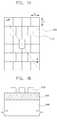
- FIG. 1is a view showing the 8F 2 cell structure of a general DRAM device.
- FIG. 2is a view showing the 4F 2 cell structure of the DRAM device.
- FIGS. 3 a and 3 bare views explaining problems caused when the 4F 2 cell structure of FIG. 2 is formed in an actual pattern.
- a pattern 100represents an active region
- F 2represents a unit region of a cell storing 1 bit
- Frepresents one minimum pitch.
- An area of a unit structure including four capacitorscan be represented by 8F 2 .
- fidelity of the pattern 100 defining the active regionis reduced.
- the finest pattern formable by a conventional, commercially available deviceis a simple line and space pattern of about 40 nm, using a resolution enhancement technique (RET).
- RETresolution enhancement technique
- the pattern shapeis a two-dimensional shape as shown in FIG. 1
- a limit of an allowable designis forced to be large. Since it is difficult to progress the fineness of the pattern using the conventional, commercially available device, a different type of cell design has been proposed.
- FIG. 2shows a proposed type of cell design, the 4F 2 cell structure.
- a pattern 200represents an active region.
- the cell area of the 4F 2 cell structurecan be theoretically reduced to half the cell area of the 8F 2 cell structure.
- a pattern 300 shape implemented when the 4F 2 cell structure is substantially formed on a waferis represented by a circle. Even in this case, it is difficult to guarantee uniformity between patterns because of a defect of resolution.
- the current exposure apparatuscannot sufficiently transfer diffraction information by a mask pattern because an interval between the patterns is too narrow. Referring to FIGS.
- a method for patterning an active region in a semiconductor device using a space patterning processincludes: forming a partition pattern having partition pattern elements arranged in a square shape on a semiconductor substrate; forming a spacer on side walls in the partition pattern elements; removing the partition pattern; separating the spacer into first and second spacer portions to expose a portion of the semiconductor substrate; and etching the exposed portion of the semiconductor substrate to form a trench, wherein a portion of the semiconductor substrate overlapped with the first and second spacer portions defines an active region.
- Elements of the partition patterncan be formed, for example, to have a rectangular or diamond shape, with any one direction longer than another direction.
- the partition pattern elementsare preferably arranged so that lines connecting the partition pattern elements form zigzags, and the partition pattern is formed in a square shape.
- the partition patternpreferably has a length of about 50 nm and a width of about 75 nm, when a pitch of the active region is set to about 75 nm in size.
- the spacerpreferably has the same etch selectivity as the partition pattern.
- the partition patternis preferably removed by a wet etching.
- the spacerpreferably remains in a square ring shape after removal of the partition pattern.
- the methodcan include separating the spacer by forming a mask pattern including an opening having a line shape that is extended across a middle portion of the spacer to expose the middle portion of the spacer; and selectively etching and removing the exposed spacer portion.
- the method of the inventioncan further include selectively removing the first and second spacer portions; removing remnants of the removed first and second spacer portions from an upper portion of the semiconductor substrate by a cleaning process; and forming an insulating layer to fill the trench.
- FIG. 1is a view showing a conventional 8F 2 cell structure of a DRAM device.
- FIG. 2is a view showing a conventional 4F 2 cell structure of a DRAM device.
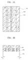
- FIGS. 3 a and 3 bare views showing problems caused when the 4F 2 cell structure of FIG. 2 is formed in an actual pattern by conventional exposure machines.
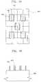
- FIGS. 4 a to 11 bare views showing a method for patterning an active region of a semiconductor device by using a space patterning process according to an embodiment of the invention.
- the inventionprovides a method that can increase the resolution of a pattern.
- a sacrifice layer 405is formed on a semiconductor substrate 400 .
- the sacrifice layer 405defines a region in which a target pattern will be formed using a space patterning technique (SPT).
- SPTspace patterning technique
- the sacrifice layer 405can be formed, for example, of an oxide layer.
- a first mask pattern 410is formed on the sacrifice layer 405 .
- the first mask pattern 410is formed by forming a resist layer on the sacrifice layer 405 .
- an exposure process irradiating light on a resist layeris performed. Physical properties of the resist layer are changed according exposure to the irradiating light.
- the first mask pattern 410which selectively exposes the sacrifice layer 405 , is formed by performing a development process on the resist layer to selectively remove a portion of the resist layer whose physical properties are changed by exposure to the irradiating light.
- F 2is a unit area of a cell storing 1 bit and F is a minimum feature size in a line end space pattern.
- the first mask pattern 410is preferably formed in a square shape.
- the first mask patternpreferably has a length of about 50 nm and a width of about 75 nm, when a minimum feature size F is set to about 75 nm.
- elements of the first mask pattern 410are formed in a rectangular shape where a length of a portion of the pattern is relatively longer than a length of the other portion.
- the first mask pattern 410 elementscan be formed to have a diamond shape.
- a portion having a long lengthis a major axis of the first mask pattern 410 and a portion having a short length is a minor axis of the first mask pattern 410 .
- FIG. 4 bis a view showing a cross section taken along a diagonal direction A-A′. Further, the figures define the feature size F as a lattice shape, but the lattice shape is not actually formed in an actual pattern.
- the exposed portion of the sacrifice layer 405(see FIG. 4 a ) is etched using the first mask pattern 410 as an etch mask to form a partition pattern 415 .
- the partition pattern 415designates a position of a target pattern to be subsequently formed, and exposes a portion of a surface of the semiconductor substrate 100 .
- the partition pattern 415is formed having partition pattern 415 elements arranged in a square shape. When a partition pattern 415 element is formed into a rectangular or diamond shape, the size of the chip can be reduced, and further, a number of partition pattern elements can be formed within a limited space.
- the partition pattern 415 elementspreferably have a length of about 50 nm and a width of about 75 nm, when a minimum feature size F is set to about 75 nm.
- the partition pattern 415 elementscan be formed, for example, to have a rectangular or diamond shape, whose any one direction is longer than other directions.
- the partition pattern 415 elementsare preferably arranged so that lines connecting the partition pattern 415 elements form zigzags.
- the partition pattern 415forms to be larger than the patterns 100 and 200 of the conventional 8F 2 or 4F 2 cell structures shown in FIGS. 1 and 2 , making it possible to increase the resolution of the pattern.
- a spacer 420is disposed on side walls of the partition pattern 415 .
- a spacer layeris formed on the partition pattern 415 and the semiconductor substrate 400 .
- the spacer layercan be formed, for example, of a nitride based insulating layer having the same etch selectivity as the partition pattern 415 .
- the spacer layercan be formed of a silicon nitride (Si 3 N 4 ) layer.
- the spacer layercan also be formed, for example, of a polysilicon layer. A portion of the spacer layer disposed on an upper portion of the partition pattern 415 and the semiconductor substrate 400 is removed, for example, by an anisotropic etching.
- the spacer 420is formed on the side walls of the partition pattern 415 .
- the spacer 420is preferably formed surrounding each surface of the partition pattern 415 , for example, in a ring shape.
- the spacer 420is preferably formed at the same thickness as a width of the active region to be subsequently formed.
- the spacer 420can be formed at a thickness in a range of 15 nm to 25 nm, projecting from each exposed surface of the partition pattern 415 . Therefore, the spacer 415 has a line width in a range of 15 nm to 25 nm.
- the spacer 420is formed around one partition pattern 415 element so as not to contact a spacer 420 formed on another partition pattern 415 element, adjacently arranged in a diagonal direction.
- the spacer 420can be formed, for example, by performing an etch back process, but the invention is not limited to the etch back process
- an etching processwhich removes the partition pattern 415 , is performed to expose a portion of the spacer 420 .
- a vertical profile side surface of the spacer 420is exposed.
- the partition pattern 415can be removed, for example, by supplying a wet etching solution chemically dissolving the partition pattern 415 . Since the partition pattern 415 has a different etch ratio than the spacer 420 , only the partition pattern 415 is selectively removed. As shown in FIG. 7 a , the spacer 420 having the ring shape remains on the semiconductor substrate 400 after the etching process.
- a second mask pattern 425which selectively exposes a portion of the spacer 420 , is formed on the semiconductor substrate 400 .
- the second mask pattern 425is formed by forming a resist layer on the semiconductor substrate. An exposures irradiating light on the resist layer is performed. The physical properties of the resist layer are then changed by exposure to the irradiating light.
- the second mask pattern 425 selectively exposing the spacer 420is formed by performing a development process on the resist layer to selectively removing a portion of the resist layer whose physical properties are changed by exposure to the irradiating light.
- the second mask pattern 425includes an opening having a line shape that is extended across a middle portion of the spacer 420 .
- the second mask pattern 425exposes a portion of a minor axis of the spacer 420 .
- the exposed portion of the spacer 420is selectively etched using the second mask pattern 425 as the etch mask.
- the spacer 420is separated into two portions, a first spacer 430 and a second spacer 435 .
- the first spacer 430 and the second spacer 435defining a portion in which the active region will be formed.
- the second spacer 435is preferably arranged as a mirror image of the first spacer 430 , and spaced by a predetermined distance from the first space 430 .
- the second mask pattern 425can be removed, for example, by performing a strip process.
- the exposed portion of the semiconductor substrate 400is etched to a predetermined depth using the first spacer 430 and the second spacer 435 as the etch mask.
- the portions of the semiconductor substrate 400 overlapped with the first and second spacers 430 and 435define the active regions.
- the first and second spacers 430 and 435are removed, and the remnants of the spacer are removed by performing a cleaning process.
- a trench 500 for isolating a deviceis formed, which defines the first and second active regions 440 , 445 on the semiconductor substrate 400 .
- the first and second active regions 440 , 445are arranged to be spaced by a predetermined distance and have a mirror image structure.
- the first and second active regions 440 and 445are established as a unit cell region that includes two capacitors in the first active region 440 and two capacitors in the second active region 445 .
- An area of the unit cell regionis formed as 1.75F 2 , when the minimum feature F size is 75 nm.
- ituses the double patterning method to form the fine pattern, it is difficult to make the overlay of the pattern elements zero such that the pattern elements are separate and distinct, and further it is difficult to make the size of the pattern elements constant.
- an insulating layer 502which fills the trench 500 for isolating the device, is formed on the semiconductor substrate 400 .
- the method for patterning the active region of the semiconductor device using the space patterning process according to the inventioncan form the active region in a stable form within an area as small as possible by first forming the pattern and then using the space patterning process and the separation process.
Landscapes
- Engineering & Computer Science (AREA)
- Chemical & Material Sciences (AREA)
- Inorganic Chemistry (AREA)
- Physics & Mathematics (AREA)
- Condensed Matter Physics & Semiconductors (AREA)
- General Physics & Mathematics (AREA)
- Manufacturing & Machinery (AREA)
- Computer Hardware Design (AREA)
- Microelectronics & Electronic Packaging (AREA)
- Power Engineering (AREA)
- Semiconductor Memories (AREA)
Abstract
Description
Claims (9)
Applications Claiming Priority (2)
| Application Number | Priority Date | Filing Date | Title |
|---|---|---|---|
| KR10-2008-0058490 | 2008-06-20 | ||
| KR1020080058490AKR100950480B1 (en) | 2008-06-20 | 2008-06-20 | Active region formation method of semiconductor device using space patterning technology |
Publications (2)
| Publication Number | Publication Date |
|---|---|
| US20090317979A1 US20090317979A1 (en) | 2009-12-24 |
| US8110507B2true US8110507B2 (en) | 2012-02-07 |
Family
ID=41431686
Family Applications (1)
| Application Number | Title | Priority Date | Filing Date |
|---|---|---|---|
| US12/331,669Expired - Fee RelatedUS8110507B2 (en) | 2008-06-20 | 2008-12-10 | Method for patterning an active region in a semiconductor device using a space patterning process |
Country Status (2)
| Country | Link |
|---|---|
| US (1) | US8110507B2 (en) |
| KR (1) | KR100950480B1 (en) |
Cited By (2)
| Publication number | Priority date | Publication date | Assignee | Title |
|---|---|---|---|---|
| US9276003B2 (en) | 2013-03-15 | 2016-03-01 | Samsung Electronics Co., Ltd. | Semiconductor devices and methods of manufacturing the same |
| US11251189B2 (en) | 2009-02-09 | 2022-02-15 | Longitude Flash Memory Solutions Ltd. | Gate fringing effect based channel formation for semiconductor device |
Families Citing this family (2)
| Publication number | Priority date | Publication date | Assignee | Title |
|---|---|---|---|---|
| KR101132803B1 (en)* | 2010-12-30 | 2012-04-02 | 주식회사 하이닉스반도체 | Method for fabricating fine pattern |
| JP2012174976A (en)* | 2011-02-23 | 2012-09-10 | Tokyo Electron Ltd | Method of forming pattern |
Citations (10)
| Publication number | Priority date | Publication date | Assignee | Title |
|---|---|---|---|---|
| US20020197823A1 (en)* | 2001-05-18 | 2002-12-26 | Yoo Jae-Yoon | Isolation method for semiconductor device |
| US6723607B2 (en)* | 2002-06-14 | 2004-04-20 | Samsung Electronics Co., Ltd. | Method of forming fine patterns of semiconductor device |
| US20040119167A1 (en) | 2002-12-10 | 2004-06-24 | Jong-Wook Suk | Semiconductor device having an active region whose width varies |
| US20050215040A1 (en)* | 2000-03-01 | 2005-09-29 | Brian Doyle | Quantum wire gate device and method of making same |
| US20060197177A1 (en) | 2005-03-03 | 2006-09-07 | Samsung Electronics Co., Ltd. | Semiconductor devices having line type active regions and methods of fabricating the same |
| KR100723527B1 (en) | 2006-02-13 | 2007-05-30 | 삼성전자주식회사 | Method for manufacturing semiconductor device having vertical channel transistor and semiconductor device manufactured thereby |
| US20070246783A1 (en) | 2006-01-05 | 2007-10-25 | Samsung Electronics Co., Ltd. | Methods of manufacturing semiconductor devices and semiconductor devices manufactured using such a method |
| KR20090042458A (en) | 2007-10-26 | 2009-04-30 | 주식회사 하이닉스반도체 | Pattern formation method of semiconductor memory device using spacer |
| KR20090047001A (en) | 2007-11-07 | 2009-05-12 | 주식회사 하이닉스반도체 | Fine Pattern Forming Method of Semiconductor Device Using Spacer |
| US7795080B2 (en)* | 2007-01-15 | 2010-09-14 | Sandisk Corporation | Methods of forming integrated circuit devices using composite spacer structures |
- 2008
- 2008-06-20KRKR1020080058490Apatent/KR100950480B1/ennot_activeExpired - Fee Related
- 2008-12-10USUS12/331,669patent/US8110507B2/ennot_activeExpired - Fee Related
Patent Citations (10)
| Publication number | Priority date | Publication date | Assignee | Title |
|---|---|---|---|---|
| US20050215040A1 (en)* | 2000-03-01 | 2005-09-29 | Brian Doyle | Quantum wire gate device and method of making same |
| US20020197823A1 (en)* | 2001-05-18 | 2002-12-26 | Yoo Jae-Yoon | Isolation method for semiconductor device |
| US6723607B2 (en)* | 2002-06-14 | 2004-04-20 | Samsung Electronics Co., Ltd. | Method of forming fine patterns of semiconductor device |
| US20040119167A1 (en) | 2002-12-10 | 2004-06-24 | Jong-Wook Suk | Semiconductor device having an active region whose width varies |
| US20060197177A1 (en) | 2005-03-03 | 2006-09-07 | Samsung Electronics Co., Ltd. | Semiconductor devices having line type active regions and methods of fabricating the same |
| US20070246783A1 (en) | 2006-01-05 | 2007-10-25 | Samsung Electronics Co., Ltd. | Methods of manufacturing semiconductor devices and semiconductor devices manufactured using such a method |
| KR100723527B1 (en) | 2006-02-13 | 2007-05-30 | 삼성전자주식회사 | Method for manufacturing semiconductor device having vertical channel transistor and semiconductor device manufactured thereby |
| US7795080B2 (en)* | 2007-01-15 | 2010-09-14 | Sandisk Corporation | Methods of forming integrated circuit devices using composite spacer structures |
| KR20090042458A (en) | 2007-10-26 | 2009-04-30 | 주식회사 하이닉스반도체 | Pattern formation method of semiconductor memory device using spacer |
| KR20090047001A (en) | 2007-11-07 | 2009-05-12 | 주식회사 하이닉스반도체 | Fine Pattern Forming Method of Semiconductor Device Using Spacer |
Cited By (3)
| Publication number | Priority date | Publication date | Assignee | Title |
|---|---|---|---|---|
| US11251189B2 (en) | 2009-02-09 | 2022-02-15 | Longitude Flash Memory Solutions Ltd. | Gate fringing effect based channel formation for semiconductor device |
| US11950412B2 (en) | 2009-02-09 | 2024-04-02 | Longitude Flash Memory Solutions Ltd. | Gate fringing effect based channel formation for semiconductor device |
| US9276003B2 (en) | 2013-03-15 | 2016-03-01 | Samsung Electronics Co., Ltd. | Semiconductor devices and methods of manufacturing the same |
Also Published As
| Publication number | Publication date |
|---|---|
| KR100950480B1 (en) | 2010-03-31 |
| US20090317979A1 (en) | 2009-12-24 |
| KR20090132294A (en) | 2009-12-30 |
Similar Documents
| Publication | Publication Date | Title |
|---|---|---|
| US7615496B2 (en) | Method of forming pad patterns using self-align double patterning method, pad pattern layout formed using the same, and method of forming contact holes using self-align double patterning method | |
| US7867912B2 (en) | Methods of manufacturing semiconductor structures | |
| US8465908B2 (en) | Method for forming fine patterns of semiconductor device | |
| US20110312184A1 (en) | Method for forming pattern of semiconductor device | |
| US8216948B2 (en) | Exposure mask and method for forming semiconductor device using the same | |
| TW200939301A (en) | Method for manufacturing a semiconductor device | |
| CN100552882C (en) | Method for forming fine patterns in semiconductor devices | |
| US8110507B2 (en) | Method for patterning an active region in a semiconductor device using a space patterning process | |
| KR20080022387A (en) | Bit line formation method of semiconductor memory device | |
| US8273522B2 (en) | Exposure mask and method for manufacturing semiconductor device using the same | |
| US20090170336A1 (en) | Method for forming pattern of semiconductor device | |
| JP2007027681A (en) | Method for manufacturing semiconductor device | |
| TWI534947B (en) | Double patterning method of forming semiconductor active areas and isolation regions | |
| US10522366B2 (en) | Method of fabricating semiconductor device | |
| JP4330523B2 (en) | Method for forming dummy layer of split gate flash memory device | |
| KR101096987B1 (en) | Exposure mask and method of forming semiconductor device using same | |
| US7615493B2 (en) | Method for forming alignment mark | |
| US20080237672A1 (en) | High density memory | |
| CN111403269B (en) | Method for manufacturing patterned structure | |
| KR20100129544A (en) | Pattern Forming Method for Negative Spacer Patterning Process | |
| KR20080069428A (en) | Manufacturing method of semiconductor device | |
| KR100905181B1 (en) | Method of forming a semiconductor device | |
| KR20120041989A (en) | Method for manufacturing semiconductor device | |
| KR20070001751A (en) | Method of forming a semiconductor device storage node contact | |
| KR20060124900A (en) | Manufacturing method of semiconductor device |
Legal Events
| Date | Code | Title | Description |
|---|---|---|---|
| AS | Assignment | Owner name:HYNIX SEMICONDUCTOR INC., KOREA, REPUBLIC OF Free format text:ASSIGNMENT OF ASSIGNORS INTEREST;ASSIGNOR:PARK, CHAN HA;REEL/FRAME:021954/0399 Effective date:20081125 | |
| ZAAA | Notice of allowance and fees due | Free format text:ORIGINAL CODE: NOA | |
| ZAAB | Notice of allowance mailed | Free format text:ORIGINAL CODE: MN/=. | |
| FEPP | Fee payment procedure | Free format text:PAYOR NUMBER ASSIGNED (ORIGINAL EVENT CODE: ASPN); ENTITY STATUS OF PATENT OWNER: LARGE ENTITY | |
| STCF | Information on status: patent grant | Free format text:PATENTED CASE | |
| FPAY | Fee payment | Year of fee payment:4 | |
| MAFP | Maintenance fee payment | Free format text:PAYMENT OF MAINTENANCE FEE, 8TH YEAR, LARGE ENTITY (ORIGINAL EVENT CODE: M1552); ENTITY STATUS OF PATENT OWNER: LARGE ENTITY Year of fee payment:8 | |
| FEPP | Fee payment procedure | Free format text:MAINTENANCE FEE REMINDER MAILED (ORIGINAL EVENT CODE: REM.); ENTITY STATUS OF PATENT OWNER: LARGE ENTITY | |
| LAPS | Lapse for failure to pay maintenance fees | Free format text:PATENT EXPIRED FOR FAILURE TO PAY MAINTENANCE FEES (ORIGINAL EVENT CODE: EXP.); ENTITY STATUS OF PATENT OWNER: LARGE ENTITY | |
| STCH | Information on status: patent discontinuation | Free format text:PATENT EXPIRED DUE TO NONPAYMENT OF MAINTENANCE FEES UNDER 37 CFR 1.362 | |
| FP | Lapsed due to failure to pay maintenance fee | Effective date:20240207 |