US8110247B2 - Laser processing for heat-sensitive mesoscale deposition of oxygen-sensitive materials - Google Patents
Laser processing for heat-sensitive mesoscale deposition of oxygen-sensitive materialsDownload PDFInfo
- Publication number
- US8110247B2 US8110247B2US11/430,636US43063606AUS8110247B2US 8110247 B2US8110247 B2US 8110247B2US 43063606 AUS43063606 AUS 43063606AUS 8110247 B2US8110247 B2US 8110247B2
- Authority
- US
- United States
- Prior art keywords
- laser
- deposit
- target
- deposition
- deposited
- Prior art date
- Legal status (The legal status is an assumption and is not a legal conclusion. Google has not performed a legal analysis and makes no representation as to the accuracy of the status listed.)
- Expired - Fee Related, expires
Links
- 239000000463materialSubstances0.000titleclaimsabstractdescription132
- 238000012545processingMethods0.000titleclaimsabstractdescription72
- QVGXLLKOCUKJST-UHFFFAOYSA-Natomic oxygenChemical group[O]QVGXLLKOCUKJST-UHFFFAOYSA-N0.000titleclaimsabstractdescription8
- 239000001301oxygenSubstances0.000titleclaimsabstractdescription8
- 229910052760oxygenInorganic materials0.000titleclaimsabstractdescription8
- 230000008021depositionEffects0.000titleabstractdescription70
- 238000000034methodMethods0.000claimsabstractdescription139
- 238000000151depositionMethods0.000claimsabstractdescription94
- 239000007789gasSubstances0.000claimsabstractdescription50
- 239000002245particleSubstances0.000claimsabstractdescription38
- 239000002243precursorSubstances0.000claimsabstractdescription37
- 239000000725suspensionSubstances0.000claimsabstractdescription22
- 230000003647oxidationEffects0.000claimsabstractdescription14
- 238000007254oxidation reactionMethods0.000claimsabstractdescription14
- 239000000443aerosolSubstances0.000claimsdescription55
- 229910052751metalInorganic materials0.000claimsdescription46
- 239000002184metalSubstances0.000claimsdescription46
- 230000006378damageEffects0.000claimsdescription35
- 239000000919ceramicSubstances0.000claimsdescription12
- 239000004065semiconductorSubstances0.000claimsdescription12
- 230000001965increasing effectEffects0.000claimsdescription11
- 239000013077target materialSubstances0.000claimsdescription7
- 239000011261inert gasSubstances0.000claimsdescription6
- 239000012700ceramic precursorSubstances0.000claimsdescription5
- 239000002082metal nanoparticleSubstances0.000claimsdescription5
- UFHFLCQGNIYNRP-UHFFFAOYSA-NHydrogenChemical compound[H][H]UFHFLCQGNIYNRP-UHFFFAOYSA-N0.000claimsdescription4
- 229910052739hydrogenInorganic materials0.000claimsdescription4
- 239000001257hydrogenSubstances0.000claimsdescription4
- 239000012704polymeric precursorSubstances0.000claimsdescription4
- UGFAIRIUMAVXCW-UHFFFAOYSA-NCarbon monoxideChemical compound[O+]#[C-]UGFAIRIUMAVXCW-UHFFFAOYSA-N0.000claimsdescription3
- 229910002091carbon monoxideInorganic materials0.000claimsdescription3
- 230000015572biosynthetic processEffects0.000claimsdescription2
- 230000001590oxidative effectEffects0.000claimsdescription2
- 230000002401inhibitory effectEffects0.000claims1
- 230000008569processEffects0.000abstractdescription80
- 238000005245sinteringMethods0.000abstractdescription15
- 238000011282treatmentMethods0.000abstractdescription9
- 238000002144chemical decomposition reactionMethods0.000abstractdescription5
- 230000003685thermal hair damageEffects0.000abstractdescription5
- 239000002699waste materialSubstances0.000abstractdescription5
- 238000006116polymerization reactionMethods0.000abstractdescription3
- 230000008859changeEffects0.000abstractdescription2
- BASFCYQUMIYNBI-UHFFFAOYSA-NplatinumChemical compound[Pt]BASFCYQUMIYNBI-UHFFFAOYSA-N0.000description34
- 239000000976inkSubstances0.000description33
- 239000002105nanoparticleSubstances0.000description27
- BQCADISMDOOEFD-UHFFFAOYSA-NSilverChemical compound[Ag]BQCADISMDOOEFD-UHFFFAOYSA-N0.000description26
- 229910052709silverInorganic materials0.000description26
- 239000004332silverSubstances0.000description26
- 229920003023plasticPolymers0.000description25
- 239000004033plasticSubstances0.000description25
- 239000000758substrateSubstances0.000description24
- 238000004519manufacturing processMethods0.000description18
- 229910052697platinumInorganic materials0.000description16
- 239000010408filmSubstances0.000description15
- 239000011521glassSubstances0.000description15
- PCHJSUWPFVWCPO-UHFFFAOYSA-NgoldChemical compound[Au]PCHJSUWPFVWCPO-UHFFFAOYSA-N0.000description14
- 229910052737goldInorganic materials0.000description14
- 239000010931goldSubstances0.000description14
- 238000000354decomposition reactionMethods0.000description13
- 238000010438heat treatmentMethods0.000description13
- 239000000243solutionSubstances0.000description13
- 230000005855radiationEffects0.000description12
- 239000010409thin filmSubstances0.000description12
- 238000000149argon plasma sinteringMethods0.000description11
- 230000008901benefitEffects0.000description11
- 238000013532laser treatmentMethods0.000description11
- 238000002844meltingMethods0.000description10
- 229920000515polycarbonatePolymers0.000description10
- 239000004417polycarbonateSubstances0.000description10
- 239000000203mixtureSubstances0.000description9
- 239000010948rhodiumSubstances0.000description9
- 239000002904solventSubstances0.000description9
- 239000012530fluidSubstances0.000description8
- 230000008018meltingEffects0.000description8
- 238000001465metallisationMethods0.000description8
- 229920003229poly(methyl methacrylate)Polymers0.000description8
- 239000004926polymethyl methacrylateSubstances0.000description8
- 229910000859α-FeInorganic materials0.000description8
- 239000004020conductorSubstances0.000description7
- 239000007788liquidSubstances0.000description7
- 238000001000micrographMethods0.000description7
- 229920000642polymerPolymers0.000description7
- 238000005336crackingMethods0.000description6
- -1polyethylene terephthalatePolymers0.000description6
- 229920000139polyethylene terephthalatePolymers0.000description6
- 239000005020polyethylene terephthalateSubstances0.000description6
- 239000000843powderSubstances0.000description6
- 238000013459approachMethods0.000description5
- 238000005137deposition processMethods0.000description5
- 230000004048modificationEffects0.000description5
- 238000012986modificationMethods0.000description5
- XKRFYHLGVUSROY-UHFFFAOYSA-NArgonChemical compound[Ar]XKRFYHLGVUSROY-UHFFFAOYSA-N0.000description4
- RYGMFSIKBFXOCR-UHFFFAOYSA-NCopperChemical compound[Cu]RYGMFSIKBFXOCR-UHFFFAOYSA-N0.000description4
- 239000004593EpoxySubstances0.000description4
- 239000012707chemical precursorSubstances0.000description4
- 229910052802copperInorganic materials0.000description4
- 239000010949copperSubstances0.000description4
- 238000001035dryingMethods0.000description4
- 239000012776electronic materialSubstances0.000description4
- 125000003700epoxy groupChemical group0.000description4
- 238000004093laser heatingMethods0.000description4
- 229910044991metal oxideInorganic materials0.000description4
- 150000004706metal oxidesChemical class0.000description4
- 150000002739metalsChemical class0.000description4
- 229920003223poly(pyromellitimide-1,4-diphenyl ether)Polymers0.000description4
- 229920000647polyepoxidePolymers0.000description4
- 238000007781pre-processingMethods0.000description4
- 230000008439repair processEffects0.000description4
- 229910052703rhodiumInorganic materials0.000description4
- 239000000523sampleSubstances0.000description4
- 239000007921spraySubstances0.000description4
- FBEIPJNQGITEBL-UHFFFAOYSA-JtetrachloroplatinumChemical compoundCl[Pt](Cl)(Cl)ClFBEIPJNQGITEBL-UHFFFAOYSA-J0.000description4
- IJGRMHOSHXDMSA-UHFFFAOYSA-NAtomic nitrogenChemical compoundN#NIJGRMHOSHXDMSA-UHFFFAOYSA-N0.000description3
- 239000004696Poly ether ether ketoneSubstances0.000description3
- 239000004642PolyimideSubstances0.000description3
- 238000012387aerosolizationMethods0.000description3
- JRPBQTZRNDNNOP-UHFFFAOYSA-Nbarium titanateChemical compound[Ba+2].[Ba+2].[O-][Ti]([O-])([O-])[O-]JRPBQTZRNDNNOP-UHFFFAOYSA-N0.000description3
- 229910002113barium titanateInorganic materials0.000description3
- 239000012159carrier gasSubstances0.000description3
- 239000000470constituentSubstances0.000description3
- 238000001816coolingMethods0.000description3
- 230000007547defectEffects0.000description3
- 238000011161developmentMethods0.000description3
- 239000003989dielectric materialSubstances0.000description3
- 238000005530etchingMethods0.000description3
- 238000009472formulationMethods0.000description3
- 239000012212insulatorSubstances0.000description3
- 238000003475laminationMethods0.000description3
- 230000003287optical effectEffects0.000description3
- 229920000728polyesterPolymers0.000description3
- 229920002530polyetherether ketonePolymers0.000description3
- 229920001721polyimidePolymers0.000description3
- 238000012805post-processingMethods0.000description3
- MHOVAHRLVXNVSD-UHFFFAOYSA-Nrhodium atomChemical compound[Rh]MHOVAHRLVXNVSD-UHFFFAOYSA-N0.000description3
- 238000009834vaporizationMethods0.000description3
- 230000008016vaporizationEffects0.000description3
- CURLTUGMZLYLDI-UHFFFAOYSA-NCarbon dioxideChemical compoundO=C=OCURLTUGMZLYLDI-UHFFFAOYSA-N0.000description2
- PXHVJJICTQNCMI-UHFFFAOYSA-NNickelChemical compound[Ni]PXHVJJICTQNCMI-UHFFFAOYSA-N0.000description2
- KDLHZDBZIXYQEI-UHFFFAOYSA-NPalladiumChemical compound[Pd]KDLHZDBZIXYQEI-UHFFFAOYSA-N0.000description2
- VYPSYNLAJGMNEJ-UHFFFAOYSA-NSilicium dioxideChemical compoundO=[Si]=OVYPSYNLAJGMNEJ-UHFFFAOYSA-N0.000description2
- XUIMIQQOPSSXEZ-UHFFFAOYSA-NSiliconChemical compound[Si]XUIMIQQOPSSXEZ-UHFFFAOYSA-N0.000description2
- 238000010521absorption reactionMethods0.000description2
- 239000000654additiveSubstances0.000description2
- 230000000996additive effectEffects0.000description2
- 239000000853adhesiveSubstances0.000description2
- 230000001070adhesive effectEffects0.000description2
- PNEYBMLMFCGWSK-UHFFFAOYSA-Naluminium oxideInorganic materials[O-2].[O-2].[O-2].[Al+3].[Al+3]PNEYBMLMFCGWSK-UHFFFAOYSA-N0.000description2
- 229910052786argonInorganic materials0.000description2
- 238000000889atomisationMethods0.000description2
- 239000013590bulk materialSubstances0.000description2
- 238000011088calibration curveMethods0.000description2
- 150000001875compoundsChemical class0.000description2
- 229920001940conductive polymerPolymers0.000description2
- 238000010017direct printingMethods0.000description2
- 230000000694effectsEffects0.000description2
- 230000005670electromagnetic radiationEffects0.000description2
- 238000005516engineering processMethods0.000description2
- 239000000835fiberSubstances0.000description2
- 238000005286illuminationMethods0.000description2
- AMGQUBHHOARCQH-UHFFFAOYSA-Nindium;oxotinChemical compound[In].[Sn]=OAMGQUBHHOARCQH-UHFFFAOYSA-N0.000description2
- 238000007641inkjet printingMethods0.000description2
- 230000001678irradiating effectEffects0.000description2
- 239000012705liquid precursorSubstances0.000description2
- 239000013307optical fiberSubstances0.000description2
- 239000003960organic solventSubstances0.000description2
- 229920003207poly(ethylene-2,6-naphthalate)Polymers0.000description2
- 239000011112polyethylene naphthalateSubstances0.000description2
- 229920001343polytetrafluoroethylenePolymers0.000description2
- 239000004810polytetrafluoroethyleneSubstances0.000description2
- 238000007639printingMethods0.000description2
- 230000009467reductionEffects0.000description2
- 238000011160researchMethods0.000description2
- 229910052710siliconInorganic materials0.000description2
- 239000010703siliconSubstances0.000description2
- SQGYOTSLMSWVJD-UHFFFAOYSA-Nsilver(1+) nitrateChemical compound[Ag+].[O-]N(=O)=OSQGYOTSLMSWVJD-UHFFFAOYSA-N0.000description2
- 230000002459sustained effectEffects0.000description2
- 230000007704transitionEffects0.000description2
- 238000009736wettingMethods0.000description2
- CQVDKGFMVXRRAI-UHFFFAOYSA-JCl[Au](Cl)(Cl)ClChemical compoundCl[Au](Cl)(Cl)ClCQVDKGFMVXRRAI-UHFFFAOYSA-J0.000description1
- 229910002601GaNInorganic materials0.000description1
- JMASRVWKEDWRBT-UHFFFAOYSA-NGallium nitrideChemical compound[Ga]#NJMASRVWKEDWRBT-UHFFFAOYSA-N0.000description1
- 238000006842Henry reactionMethods0.000description1
- PWHULOQIROXLJO-UHFFFAOYSA-NManganeseChemical compound[Mn]PWHULOQIROXLJO-UHFFFAOYSA-N0.000description1
- 229910001289Manganese-zinc ferriteInorganic materials0.000description1
- KJTLSVCANCCWHF-UHFFFAOYSA-NRutheniumChemical compound[Ru]KJTLSVCANCCWHF-UHFFFAOYSA-N0.000description1
- 229920006362Teflon®Polymers0.000description1
- 229910007948ZrB2Inorganic materials0.000description1
- JIYIUPFAJUGHNL-UHFFFAOYSA-N[O--].[O--].[O--].[O--].[O--].[O--].[O--].[O--].[O--].[O--].[O--].[O--].[O--].[O--].[O--].[O--].[O--].[O--].[O--].[O--].[Mn++].[Mn++].[Mn++].[Fe+3].[Fe+3].[Fe+3].[Fe+3].[Fe+3].[Fe+3].[Fe+3].[Fe+3].[Fe+3].[Fe+3].[Zn++].[Zn++]Chemical compound[O--].[O--].[O--].[O--].[O--].[O--].[O--].[O--].[O--].[O--].[O--].[O--].[O--].[O--].[O--].[O--].[O--].[O--].[O--].[O--].[Mn++].[Mn++].[Mn++].[Fe+3].[Fe+3].[Fe+3].[Fe+3].[Fe+3].[Fe+3].[Fe+3].[Fe+3].[Fe+3].[Fe+3].[Zn++].[Zn++]JIYIUPFAJUGHNL-UHFFFAOYSA-N0.000description1
- 230000009471actionEffects0.000description1
- 239000002390adhesive tapeSubstances0.000description1
- 229910045601alloyInorganic materials0.000description1
- 239000000956alloySubstances0.000description1
- 238000005275alloyingMethods0.000description1
- 229910021417amorphous siliconInorganic materials0.000description1
- 239000007864aqueous solutionSubstances0.000description1
- VWZIXVXBCBBRGP-UHFFFAOYSA-Nboron;zirconiumChemical compoundB#[Zr]#BVWZIXVXBCBBRGP-UHFFFAOYSA-N0.000description1
- 239000006227byproductSubstances0.000description1
- 239000003990capacitorSubstances0.000description1
- 239000001569carbon dioxideSubstances0.000description1
- 229910002092carbon dioxideInorganic materials0.000description1
- 238000010382chemical cross-linkingMethods0.000description1
- 238000003486chemical etchingMethods0.000description1
- 238000001311chemical methods and processMethods0.000description1
- 238000012993chemical processingMethods0.000description1
- 238000006243chemical reactionMethods0.000description1
- 238000004140cleaningMethods0.000description1
- 238000004581coalescenceMethods0.000description1
- 239000002131composite materialSubstances0.000description1
- 230000001143conditioned effectEffects0.000description1
- 238000011109contaminationMethods0.000description1
- 238000007796conventional methodMethods0.000description1
- HFDWIMBEIXDNQS-UHFFFAOYSA-Lcopper;diformateChemical compound[Cu+2].[O-]C=O.[O-]C=OHFDWIMBEIXDNQS-UHFFFAOYSA-L0.000description1
- 238000002425crystallisationMethods0.000description1
- 230000008025crystallizationEffects0.000description1
- 230000003247decreasing effectEffects0.000description1
- 238000000280densificationMethods0.000description1
- 230000001419dependent effectEffects0.000description1
- 238000005553drillingMethods0.000description1
- 230000005294ferromagnetic effectEffects0.000description1
- 239000003302ferromagnetic materialSubstances0.000description1
- 230000004907fluxEffects0.000description1
- 239000011888foilSubstances0.000description1
- 229910052732germaniumInorganic materials0.000description1
- GNPVGFCGXDBREM-UHFFFAOYSA-Ngermanium atomChemical compound[Ge]GNPVGFCGXDBREM-UHFFFAOYSA-N0.000description1
- NNGHIEIYUJKFQS-UHFFFAOYSA-Lhydroxy(oxo)iron;zincChemical compound[Zn].O[Fe]=O.O[Fe]=ONNGHIEIYUJKFQS-UHFFFAOYSA-L0.000description1
- 230000003116impacting effectEffects0.000description1
- 230000001939inductive effectEffects0.000description1
- 238000009413insulationMethods0.000description1
- 239000000696magnetic materialSubstances0.000description1
- 229910052748manganeseInorganic materials0.000description1
- 239000011572manganeseSubstances0.000description1
- 239000011159matrix materialSubstances0.000description1
- 238000005259measurementMethods0.000description1
- 239000007769metal materialSubstances0.000description1
- 238000004377microelectronicMethods0.000description1
- 238000012544monitoring processMethods0.000description1
- 239000006199nebulizerSubstances0.000description1
- 229910052759nickelInorganic materials0.000description1
- 229910052757nitrogenInorganic materials0.000description1
- JCXJVPUVTGWSNB-UHFFFAOYSA-Nnitrogen dioxideInorganic materialsO=[N]=OJCXJVPUVTGWSNB-UHFFFAOYSA-N0.000description1
- TWNQGVIAIRXVLR-UHFFFAOYSA-Noxo(oxoalumanyloxy)alumaneChemical compoundO=[Al]O[Al]=OTWNQGVIAIRXVLR-UHFFFAOYSA-N0.000description1
- 238000004806packaging method and processMethods0.000description1
- 229910052763palladiumInorganic materials0.000description1
- 230000037361pathwayEffects0.000description1
- 238000000059patterningMethods0.000description1
- SLIUAWYAILUBJU-UHFFFAOYSA-NpentaceneChemical compoundC1=CC=CC2=CC3=CC4=CC5=CC=CC=C5C=C4C=C3C=C21SLIUAWYAILUBJU-UHFFFAOYSA-N0.000description1
- 230000002093peripheral effectEffects0.000description1
- 230000002186photoactivationEffects0.000description1
- 229920000307polymer substratePolymers0.000description1
- 238000003672processing methodMethods0.000description1
- 238000004080punchingMethods0.000description1
- 238000001953recrystallisationMethods0.000description1
- 229910001925ruthenium oxideInorganic materials0.000description1
- WOCIAKWEIIZHES-UHFFFAOYSA-Nruthenium(iv) oxideChemical compoundO=[Ru]=OWOCIAKWEIIZHES-UHFFFAOYSA-N0.000description1
- 150000003839saltsChemical class0.000description1
- 238000012216screeningMethods0.000description1
- 230000035939shockEffects0.000description1
- 235000012239silicon dioxideNutrition0.000description1
- 239000000377silicon dioxideSubstances0.000description1
- CQLFBEKRDQMJLZ-UHFFFAOYSA-Msilver acetateChemical compound[Ag+].CC([O-])=OCQLFBEKRDQMJLZ-UHFFFAOYSA-M0.000description1
- 229940071536silver acetateDrugs0.000description1
- 229910001961silver nitrateInorganic materials0.000description1
- 239000007787solidSubstances0.000description1
- 238000003892spreadingMethods0.000description1
- 230000007480spreadingEffects0.000description1
- 239000000126substanceSubstances0.000description1
- MZLGASXMSKOWSE-UHFFFAOYSA-Ntantalum nitrideChemical compound[Ta]#NMZLGASXMSKOWSE-UHFFFAOYSA-N0.000description1
- 238000012360testing methodMethods0.000description1
- 230000026683transductionEffects0.000description1
- 238000010361transductionMethods0.000description1
- 238000009966trimmingMethods0.000description1
- 238000005406washingMethods0.000description1
Images


Classifications
- H—ELECTRICITY
- H05—ELECTRIC TECHNIQUES NOT OTHERWISE PROVIDED FOR
- H05K—PRINTED CIRCUITS; CASINGS OR CONSTRUCTIONAL DETAILS OF ELECTRIC APPARATUS; MANUFACTURE OF ASSEMBLAGES OF ELECTRICAL COMPONENTS
- H05K3/00—Apparatus or processes for manufacturing printed circuits
- H05K3/10—Apparatus or processes for manufacturing printed circuits in which conductive material is applied to the insulating support in such a manner as to form the desired conductive pattern
- H05K3/102—Apparatus or processes for manufacturing printed circuits in which conductive material is applied to the insulating support in such a manner as to form the desired conductive pattern by bonding of conductive powder, i.e. metallic powder
- H—ELECTRICITY
- H05—ELECTRIC TECHNIQUES NOT OTHERWISE PROVIDED FOR
- H05K—PRINTED CIRCUITS; CASINGS OR CONSTRUCTIONAL DETAILS OF ELECTRIC APPARATUS; MANUFACTURE OF ASSEMBLAGES OF ELECTRICAL COMPONENTS
- H05K3/00—Apparatus or processes for manufacturing printed circuits
- H05K3/10—Apparatus or processes for manufacturing printed circuits in which conductive material is applied to the insulating support in such a manner as to form the desired conductive pattern
- H05K3/105—Apparatus or processes for manufacturing printed circuits in which conductive material is applied to the insulating support in such a manner as to form the desired conductive pattern by conversion of non-conductive material on or in the support into conductive material, e.g. by using an energy beam
- H—ELECTRICITY
- H05—ELECTRIC TECHNIQUES NOT OTHERWISE PROVIDED FOR
- H05K—PRINTED CIRCUITS; CASINGS OR CONSTRUCTIONAL DETAILS OF ELECTRIC APPARATUS; MANUFACTURE OF ASSEMBLAGES OF ELECTRICAL COMPONENTS
- H05K2203/00—Indexing scheme relating to apparatus or processes for manufacturing printed circuits covered by H05K3/00
- H05K2203/08—Treatments involving gases
- H05K2203/086—Using an inert gas
- H—ELECTRICITY
- H05—ELECTRIC TECHNIQUES NOT OTHERWISE PROVIDED FOR
- H05K—PRINTED CIRCUITS; CASINGS OR CONSTRUCTIONAL DETAILS OF ELECTRIC APPARATUS; MANUFACTURE OF ASSEMBLAGES OF ELECTRICAL COMPONENTS
- H05K2203/00—Indexing scheme relating to apparatus or processes for manufacturing printed circuits covered by H05K3/00
- H05K2203/08—Treatments involving gases
- H05K2203/087—Using a reactive gas
- H—ELECTRICITY
- H05—ELECTRIC TECHNIQUES NOT OTHERWISE PROVIDED FOR
- H05K—PRINTED CIRCUITS; CASINGS OR CONSTRUCTIONAL DETAILS OF ELECTRIC APPARATUS; MANUFACTURE OF ASSEMBLAGES OF ELECTRICAL COMPONENTS
- H05K2203/00—Indexing scheme relating to apparatus or processes for manufacturing printed circuits covered by H05K3/00
- H05K2203/10—Using electric, magnetic and electromagnetic fields; Using laser light
- H05K2203/107—Using laser light
- H—ELECTRICITY
- H05—ELECTRIC TECHNIQUES NOT OTHERWISE PROVIDED FOR
- H05K—PRINTED CIRCUITS; CASINGS OR CONSTRUCTIONAL DETAILS OF ELECTRIC APPARATUS; MANUFACTURE OF ASSEMBLAGES OF ELECTRICAL COMPONENTS
- H05K2203/00—Indexing scheme relating to apparatus or processes for manufacturing printed circuits covered by H05K3/00
- H05K2203/13—Moulding and encapsulation; Deposition techniques; Protective layers
- H05K2203/1333—Deposition techniques, e.g. coating
- H05K2203/1344—Spraying small metal particles or droplets of molten metal
- Y—GENERAL TAGGING OF NEW TECHNOLOGICAL DEVELOPMENTS; GENERAL TAGGING OF CROSS-SECTIONAL TECHNOLOGIES SPANNING OVER SEVERAL SECTIONS OF THE IPC; TECHNICAL SUBJECTS COVERED BY FORMER USPC CROSS-REFERENCE ART COLLECTIONS [XRACs] AND DIGESTS
- Y10—TECHNICAL SUBJECTS COVERED BY FORMER USPC
- Y10S—TECHNICAL SUBJECTS COVERED BY FORMER USPC CROSS-REFERENCE ART COLLECTIONS [XRACs] AND DIGESTS
- Y10S428/00—Stock material or miscellaneous articles
- Y10S428/901—Printed circuit
Definitions
- the present inventionrelates generally to the field of maskless direct write deposition of materials, including but not limited to mesoscale electronic structures, using aerodynamic focusing of an aerosolized fluid or particle suspension onto heat-sensitive targets, wherein laser radiation is preferably used to process the deposit to its final state.
- Thick film and thin film processesfor the deposition of electronic structures are well developed, but have limitations due to the high processing temperatures required, or due to the need for expensive masks and vacuum chambers. Thick film processes typically require processing temperatures ranging from approximately 500 to 1000° C. Thin film techniques use processing temperatures ranging from approximately 400 to 3000° C., depending on the type of process and the material deposited. Due to inherent high processing temperatures, thick film and thin film techniques are generally limited to deposition onto ceramic, glass, silicon, and other targets having a damage threshold temperature above approximately 400° C.
- a thin film process used to form ceramic metallo-organic thin filmsis disclosed in U.S. Pat. No. 5,064, 684.
- This processcasts a liquid metallo-organic ceramic precursor solution to form a layer on a target.
- the depositis heated to a low temperature to create an amorphous layer.
- the processthen heats a selected area to a high temperature using localized heating, creating a patterned area of polycrystalline ceramic having electro-optic properties.
- Kydduses a mixture of metal powders and metallo-organic decomposition compounds in an organic liquid vehicle to form thick films.
- the compoundis applied to a target using a deposition process such as silk screening, in which bonding is complete at temperatures of less than 450° C.
- Kydd, et al.teach a composition having a metal powder or powders of specified characteristics in a Reactive Organic Medium (ROM) that can be deposited to produce patterns of electrical conductors on temperature-sensitive electronic targets.
- the patternscan be thermally cured in seconds to form pure metal conductors at a temperature low enough to avoid target damage.
- the M 3 DTM processis a direct printing technique that does not require the use of vacuum chambers, masks, or extensive post-deposition processing.
- the M 3 DTM processmay be used to deposit a variety of materials with little or no material waste, and has also been used to deposit materials which do not require high temperature processing on low temperature substrates.
- various low temperature ink systemshave been developed. These inks are typically either precursor-based, nanoparticle-based, or they can be combinations of the two.
- Metal-organic precursor chemistrieshave a specific advantage in that the precursors can decompose to pure metal at very low temperatures, 150-250° C. range. Because of this the inks can be deposited on many plastics and then heated to decompose to metal. The drawback is that the metal yield of precursor inks is typically low and is in the 1-10% range. The low yield reduces the overall deposition rates.
- Metal nanoparticlesalso have drastically reduced treatment temperatures. Because of their high surface energy, nanoparticles will melt at temperatures hundreds of degrees lower than micron-sized particles. Nanoparticle inks in particular have been shown to sinter in the 150-250° C. range. The metal yield of nanoparticle inks can be in the 10-50% range, which leads to highly efficient deposition.
- the M 3 DTM processhas been used to deposit and laser process silver (at 150° C.) on an FR4 substrate, which has a damage threshold of less than 200° C., with no damage to the substrate.
- Glassesmay undergo crystallization and melting, and metals may undergo oxidation, recrystallization, grain growth, reversed hardening, and melting, when subjected to excessive heat. Ceramics may also undergo thermal damage in the form of unfavorable phase changes that may lead to cracking or loss of material or electrical properties, vaporization of volatile components, and oxidation (for ceramics that are not oxides). For example, densification on low temperature substrates has only been achievable for materials that can be densified at temperatures below the damage threshold of the substrate.
- the present inventionis a method and apparatus for depositing a material on a target, comprising generating an aerosol stream, depositing the aerosol stream onto the target using an aerosol jet; processing the resulting deposit with a laser to obtain the material; wherein the processing temperature of the deposit is approximately at least as high as a damage threshold temperature of the target, and wherein an electrical property of the deposit is substantially similar to the electrical property of the material in bulk form.
- the electrical propertypreferably comprises resistivity and the target is optionally nonplanar.
- the damage thresholdis preferably less than 200° C.
- the aerosol streampreferably comprises one or more materials selected from the groups consisting of liquid molecular chemical precursors and colloidal or particle suspensions.
- the aerosol streampreferably further comprises one or more materials generated from the groups comprising a metallo-organic precursor, a metallo-organic precursor; a colloidal metal solution; a metal paste; a metal nanoparticle suspension; a ceramic precursor; a ceramic paste; a resistor precursor solution; a resistor paste; an inorganic semiconductor suspension; a polymeric precursor solution; a colloidal suspension of metal, dielectric, or resistor particles; and any combination thereof.
- the aerosol streampreferably comprises droplets or particles having a diameter of less than approximately 10 microns.
- the generating steppreferably comprises using ultrasonic transduction or pneumatic aerosolization.
- the aerosol jetpreferably comprises an annular flow, preferably an inner aerosol-laden flow surrounded by a sheath gas flow that confines the inner aerosol-laden flow.
- the annular flowpreferably focuses the aerosol stream to mesoscale dimensions.
- the deposited feature sizeis preferably greater than or equal to approximately four microns.
- the feature size of the deposit after laser processingis preferably at least approximately one micron.
- the depositing steppreferably comprises providing relative motion of the target and the aerosol stream.
- the methodpreferably further comprises the step of pre-processing the aerosol stream prior to the depositing step.
- the pre-processing steppreferably comprises a process selected from the group consisting of humidifying the aerosol stream, drying the aerosol stream, cooling the aerosol stream, increasing the vapor content of a constituent of the aerosol stream, and increasing the vapor content of a second material that is not a constituent of the aerosol stream.
- the targetpreferably comprises a material selected from the group consisting of polycarbonate, polyethylene terephthalate, polymethyl methacrylate, polytetrafluoroethylene, polyester, and various epoxies.
- the laserpreferably comprises a diode laser.
- the laser poweris preferably approximately 10 milliwatts.
- the laserpreferably comprises a continuous wave mode or a pulsed wave mode.
- the energy of the pulsed wave modeis preferably several microjoules.
- the processing steppreferably comprises delivering a laser beam to the target using either or both of a system of lenses and mirrors and an optical fiber.
- the laser beamis optionally delivered to the target apart from the aerosol stream, thereby resulting in serial process deposition and laser processing.
- the present inventionis also a method for depositing a material on a target comprising the steps of generating an aerosol stream of a material, propelling the aerosol stream to the target using an aerosol jet comprising an annular sheath gas, covering a resulting deposit of the material with a cover gas, and processing the resulting deposit of the material with a laser at a processing temperature approximately at least as high as a damage threshold temperature of the target.
- the cover gaspreferably comprises an inert gas, which preferably inhibits oxide formation of the material deposit.
- the cover gaspreferably comprises a reactive gas, creating a forming gas.
- the reactive gaspreferably comprises hydrogen or carbon monoxide.
- the methodpreferably further comprises the step of reducing oxides or the oxidation state of the deposited material, or increasing the conductivity or reducing the resistivity of the deposit.
- the reactive gasoptionally comprises oxygen.
- the methodoptionally further comprises the step of oxidizing the deposited material, or increasing the resistivity of the deposited material.
- the covering stepis preferably performed simultaneously with the processing step.
- the covering stepis optionally performed simultaneously with the propelling step.
- the covering steppreferably comprises streaming the cover gas over the deposit.
- the damage threshold temperatureis optionally less than 200° C.
- the aerosol streampreferably further comprises one or more materials generated from the groups consisting of a metallo-organic precursor; a colloidal metal solution; a metal paste; a metal nanoparticle suspension; a ceramic precursor; a ceramic paste; a resistor precursor solution; a resistor paste; an inorganic semiconductor suspension; a polymeric precursor solution; a colloidal suspension of metal, dielectric, or resistor particles; an oxide; and any combination thereof.
- the aerosol streampreferably comprises droplets or particles having a diameter of less than approximately 10 microns.
- the aerosol jetpreferably comprises an inner aerosol-laden flow surrounded by a sheath gas flow that confines the inner aerosol-laden flow.
- the annular sheath gaspreferably focuses the aerosol stream to mesoscale dimensions.
- the deposited feature sizeis preferably as low as approximately four microns.
- the feature size of the deposit after laser processingis preferably as low as approximately one micron.
- An object of the present inventionis to provide a maskless non-contact process for deposition of a mesoscale structure onto a heat-sensitive target or substrate.
- Another object of the present inventionis to provide a process for depositing a mesoscale structure onto a heat-sensitive target using an aerosol jet to focus and deposit an aerosol stream in a pre-determined pattern.
- An advantage of the present inventionis that it may be used to deposit materials including but not limited to conductors, semiconductors, insulators, and resistive and inductive structures.
- Another advantage of the present inventionis that low damage threshold target materials may be deposited on, including but not limited to plastics, ceramics, epoxies, and biological tissue.
- a further advantage of the present inventionis that the desired structure may be deposited onto a planar or non-planar target.
- FIG. 1is a drawing of the main components of the M 3 DTM system, shown with a pneumatic aerosolizer;
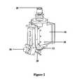
- FIG. 2is a drawing of the M 3 DTM deposition module
- FIG. 3is a flowchart showing the steps used in conventional flex circuit fabrication and those used in the M 3 DTM process for the same application;
- FIG. 4is a micrograph of an inductor fabricated using the M 3 DTM process
- FIG. 5shows an inductance curve
- FIG. 6is a micrograph of the intersection of a thermocouple junction and the lead wires
- FIG. 7shows a calibration curve for an M 3 DTM fabricated thermocouple
- FIGS. 8 a and 8 bare micrographs of sintered silver lines on polycarbonate.
- FIG. 9is a micrograph of laser treated silver interconnects on a PMMA substrate.
- the present inventionprovides a method for maskless, non-contact direct printing of mesoscale structures of various materials onto heat-sensitive targets.
- Material depositionis preferably accomplished using the M 3 DTM aerosol-jetting device, which utilizes an aerosolized stream delivered to the target via an annularly flowing aerosol jet.
- the methodpreferably uses low-power laser radiation to heat the aerosol-jetted material to its final state.
- Combining the M 3 DTM process with laser processingextends the utilization of the technique to temperature sensitive applications, in which the temperature required to treat the deposited material approaches or exceeds the thermal damage threshold of the target.
- the processis capable of precise, selective deposition with little or no material waste.
- a positional accuracy of approximately 1 micronis achievable with laser processing and a subsequent material removal process, such as etching or rinsing, with a tool-to-target standoff distance of as much as approximately five millimeters.
- heat-sensitive processmeans any process in which the temperature required to process the deposited material, i.e. drive it to its desired state, approaches or exceeds the damage threshold of the target, wherein the target is not globally heated above its damage threshold. Typically, such targets have a low damage threshold.
- a heat-sensitive processmay have a wide range of temperatures.
- Laser processing of M 3 DTM-deposited structurespreferably combines highly localized aerodynamic deposition of material with a highly localized energy source providing the ability to focus laser radiation to a diameter that is approximately the same as the width of the deposited line, to engineer material formulations to be highly absorbing at the laser wavelength, to deposit nanoparticle suspensions, and to deliver laser energy in short pulses or by rapidly scanning over a deposit enables processing of various materials onto heat-sensitive targets with little or no damage to the target.
- the present inventionis capable of depositing materials at room temperature. Many of these materials can cure at room temperature.
- One advantage offered by the inventionis the ability to lay down materials in patterns in the mesoscale range (from 1 to 1000 microns). If the material needs a thermal post treatment, the deposition can be followed with a laser treatment.
- the laser beamprovides a highly localized thermal and photonic treatment of the material. The laser beam is capable of treating only the deposited material after deposition without affecting the underlying substrate.
- the present inventionallows for a variety of substrate treatments during the deposition process.
- Alternative embodiments of the inventioninclude capabilities for heating the substrate by laser illumination or by increasing the ambient temperature.
- the substratemay also be cooled during deposition by reducing ambient temperature.
- Other alternative treatment stepsmay include photoactivation with a laser, irradiation with infrared light, or illumination with an arc lamp.
- Another substrate treatmentcomprises a washing or rinsing process.
- Typical thick film techniquesdeposit materials that must be fired well above 400° C., limiting the process to high-temperature substrates.
- the present inventionis capable of depositing materials onto heat-sensitive substrates, and then using thermal or laser processing to obtain the desired properties by virtue of the initial precursor chemistry or localized laser heating.
- the present inventioncan deposit electronic materials onto low-cost polymer substrates that cannot withstand high-temperature oven fires.
- the materialsare deposited, they are optionally post-treated to produce desired electrical and mechanical properties. This can be done either thermally or by a laser processing step depending upon the deposition material and substrate combination being used.
- the present inventioncomprises a maskless deposition process that fills a niche in the mesoscale regime between thick and thin film.
- the inventionis capable of depositing multiple materials into fine geometries on both planar and curved substrates.
- the materialscan be commercial pastes or custom, low-fire inks.
- Laser processingallows the materials to be densified on heat-sensitive polymers.
- the present inventionmay be applied to a wide range of applications.
- the ability to deposit fine lines over curved and stepped surfacesuggests applications in writing interconnect wires between IC chips and PWB.
- the ability to deposit multiple materialslends to applications in multilayer components as well as to encapsulating components once they are built.
- the ability to fire materials on heat-sensitive substrateallows discrete components to be directly written on polymers.
- the present inventionis also capable of depositing oxygen-sensitive materials. Certain materials such as copper and nickel are susceptible to oxidation, particularly at the elevated temperatures needed to sinter nanoparticle compositions of these materials.
- the present inventionenables simultaneous application of thermal processing, for example laser treatment, and a cover gas to the jetted material.
- the cover gaspreferably comprises an inert gas such as argon, nitrogen, or carbon dioxide for preventing oxidation of the material during laser treatment.
- the cover gasmay optionally comprise a combination of an inert gas such as nitrogen or argon and one or more reactive gases such as hydrogen or carbon monoxide, in which case the mixture is known as a forming gas.
- a forming gaspreferably comprises only a small percentage of the reactive gas and is preferably used when oxides are present in the material and need to be removed.
- the reactive gaspreferably reacts with the materials during laser heating to reduce the oxides present in the material. In the case of metal deposition, this results in a more conductive material, since the non-conductive metal oxides are converted into conductive metal.
- the reactive gasmay alternatively comprise oxygen, in which case the oxygen preferably reacts with the metals during laser treatment to form a metal oxide.
- the metal oxidescan be useful to tailor the deposits for a specific resistance value.
- a cover gasmay also be used during deposition and/or thermal processing of non-metallic materials to control oxide contamination and the amount of oxidation of the material.
- many semiconductorsoxidize rapidly at elevated temperature, and semiconductor nanoparticles are especially susceptible to oxidation because of the high surface area of nanoparticle compositions.
- An inert cover gascan inhibit such oxidation during laser treatment.
- the properties of the depositalso depend on the method of applying the cover gas. For example, if the cover gas is applied to the deposit as a gas jet or stream, preferably via a cover gas jet orifice of the deposition system, the resistance of the deposit is approximately a factor of two lower than that achieved when the deposition enclosure is simply flooded with the cover gas.
- the deposition technique used in the present inventionis called Maskless Mesoscale Material Deposition (M 3 DTM).
- the techniqueuses an annularly flowing aerosol jet to deposit features as small as approximately 4 microns.
- the jetconsists of an inner aerosol-laden flow surrounded by a sheath gas flow that confines and focuses the inner flow.
- the two flowsmay also consist of fluids. Focusing of the aerosol stream to one-tenth of the exit orifice diameter has been demonstrated at distances of up to approximately five millimeters from the orifice.
- the orifice diameterpreferably ranges from 100-500 microns.
- the aerosol streamis preferably formed by aerosolizing a sample using an ultrasonic transducer and/or pneumatic nebulizer 22 , as shown in FIG. 1 .
- the aerosol streamis preferably comprised of a liquid molecular chemical precursor and/or colloidal or particle or nanoparticle suspension. These preferably further comprise a metallo-organic precursor; a colloidal metal solution; a metal paste; a ceramic precursor; a ceramic paste; a resistor precursor solution; a resistor paste; an inorganic semiconductor suspension; a polymeric precursor solution; a colloidal suspension of metal, dielectric, or resistor particles, or the like, or any combination thereof.
- any material suitable for laser heatingcan be employed as a feedstock in the practice of the present invention, depending on the intended application.
- dielectric materialssuch as barium titanate or silicon dioxide, resistive materials such as a ruthenates, metal dielectric composites such as silver+barium titanate, conductive materials such as silver, copper, or gold, semiconducting materials such as silicon, germanium, or gallium nitride, magnetic materials such as MnZn and FeZn, ceramics such as alumina or zirconium diboride, and cermets may all be deposited.
- the precursor solvent or suspending fluid usedis preferably chosen based on its compatibility with the target material.
- the M 3 DTM apparatuspreferably comprises an upper module for aerosolizing liquid chemical precursors or colloidal or particle suspensions, a deposition module for directing, focusing, and depositing the resulting aerosol, laser module 10 for delivering and focusing laser radiation, and a control module for monitoring and controlling the process parameters.
- the M 3 DTM deposition moduledetailed in FIG. 2 , preferably consists of virtual impactor 24 , flowhead 12 , and material shutter assembly 26 with mechanical shutter 28 .
- the aerosol streampreferably is processed by virtual impactor 24 , which reduces the volume of gas in which the aerosol is entrained.
- the aerosol-laden carrier gaspreferably bypasses virtual impactor 24 , and enters flowhead 12 immediately after the aerosolization process.
- the carrier gaspreferably comprises either or both of a compressed air or an inert gas, and can comprise a solvent vapor.
- a flow controllerpreferably monitors and controls the mass throughput of the aerosolized stream.
- the aerosolized streampreferably enters flowhead 12 via aerosol inlet 20 in heater assembly 16 mounted on the apparatus, and is preferably collimated as it flows through an orifice centered on the longitudinal axis of flowhead 12 .
- Heater assembly 16is preferably used to heat the aerosolized material to remove solvent or to modify the viscosity of the sample.
- the aerosol streamemerges with droplets and/or particles and is preferably entrained and surrounded by a sheath gas.
- the sheath gascomprises either or both of a compressed air or an inert gas, and can optionally comprise solvent vapor content or a fluid.
- the sheath gasenters through sheath air inlet 18 , preferably located on heater assembly 16 below the aerosol inlet 20 , and then enters the lower portion of flowhead 12 , preferably through multiple internal ports, forming an annular flow surrounding the aerosol stream.
- the two streamsexit the chamber through a second orifice directed at the target.
- the sheath gasforms a boundary layer that prevents particles from depositing onto the orifice wall.
- the annular flowexits flowhead 12 through a nozzle directed at the target.
- This annular configurationis capable of focusing the aerosol stream to approximately one-fifth to one-tenth the size of the orifice diameter, enabling deposition of features on the target with dimensions as small as approximately 4 microns.
- the standoff distance between the system's flowhead and the targetis typically 3 to 5 mm, enabling deposition onto non-planar surfaces.
- Patternsare preferably written by translating a computer-controlled target platen, located under stationary flowhead 12 , using a CAD-based Virtual MaskingTM (VMToolTM) software application.
- VMToolTMVirtual MaskingTM
- flowhead 12may be translated under computer control while maintaining the target in a fixed position, or both flowhead 12 and the target may be moved simultaneously.
- Softwaresuch as VMToolTM, preferably defines a toolpath for printing the desired circuit or element.
- the deposited materialis processed with at least one laser.
- deposited materialmay be processed at a higher temperature than the damage threshold of the target to drive the deposit to the desired state in order achieve physical, optical, or electrical properties near that of the bulk material, preferably with little or no physical, chemical, optical changes, or other damage to the underlying target.
- the processingmay comprise chemical decomposition, polymerization, sintering, melting, or the like.
- Target materialsmay comprise any material with a low damage threshold temperature, including but are not limited to polymers, glasses, metals, various epoxies, and ceramics, more specifically such materials as polycarbonate, polyethylene terephthalate (PET), polymethyl methacrylate (PMMA), polytetrafluoroethylene (Teflon®), and polyester.
- PETpolyethylene terephthalate
- PMMApolymethyl methacrylate
- Teflon®polytetrafluoroethylene
- the targetmay be locally heated above its damage threshold without impact its global properties. Further, in many cases this local heating improves adhesion of the deposited material to the target.
- the present inventionprovides for processing a deposit at temperatures of up to approx. 50° C. or more higher than the damage threshold of the target. With the laser treatment of the present invention, sintering inks on low-melting-temperature plastics is possible.
- the size of the depositis in the mesoscale range, and can vary from several microns to approximately 1 millimeter, bridging the gap between thin film and thick film processes.
- the aerosol streammay optionally be pre-processed prior to deposition, most commonly before introduction of the aerosol into the flowhead.
- the pre-processing stepmay comprise processes including but not limited to increasing the solvent or suspending medium vapor content, partially decomposing, humidifying, drying, heating, or cooling of the aerosol, carrier gas, and/or sheath gas.
- the targetis optionally conditioned by heating before deposition, preferably via a heater, infrared lamp, or high power diode laser.
- the deposited patternmay also optionally be post-processed prior to the laser treatment.
- Post-processingoptionally comprises thermally heating the deposit in an ambient or reduced pressure environment, irradiating the deposit with electromagnetic radiation, or a combination thereof.
- These optional steps processingare preferably performed to remove solvent or other residual volatile constituents of the precursor solvent or the particle suspending fluid.
- dryingit is preferably performed in a manner such that the deposit retains some of its fluid properties, so that wetting and coalescence of the aerosol droplets into a continuous structure is accomplished. In this manner, the amount of laser energy required for heating and vaporization of the solvent is reduced.
- deposition and processing of the aerosol streammay optionally be performed simultaneously.
- the type of processing laser usedmay vary, and is dependent on the optical and thermal properties of the deposit and the target.
- the laser powermay be as small as approximately 10 milliwatts, enabling the use of an inexpensive diode laser.
- the lasermay comprise a continuous wave mode or a pulsed wave mode.
- the pulsed wave modeoptionally comprises an energy as low as several microjoules.
- the laser beamis preferably delivered to the target using a series of mirrors and lenses that collimate and route the beam to a focusing lens.
- the beammay optionally be delivered using fiber optics, wherein the laser beam is launched into an appropriate optical fiber and delivered through the fiber to the focusing lens.
- the laser radiationis preferably to a spot size of less than one micron. Modification of the laser beam profile facilitates material processing on heat-sensitive targets.
- the laser beamis preferably expanded and collimated before being truncated and focused onto the target.
- the expansion of the beamis performed to decrease the focused spot size, and to aid in truncation.
- Truncation of the beamminimizes the inherent Gaussian variation in laser power across the beam profile.
- the truncation stepallows for more uniform heating of the deposited line in the direction perpendicular to the target motion, and aids in the reduction of target damage at the boundaries of the deposit.
- the wavelength of the laseris preferably chosen so that laser radiation is absorbed by the deposit but not by the target. That is, ideally the deposit is highly absorptive and the target is highly transmissive, that is, transparent or nearly transparent, at the wavelength of the laser.
- the materialmay be sintered, decomposed, or otherwise processed, and most of the heat delivered to the target is the heat conducted through the deposit/target interface.
- the target materialis highly absorbing at the laser wavelength, and the deposit is weakly absorbing. In this case, the deposit is heated through conduction of thermal energy from the target/deposit boundary. The former case is ideal for laser processing of heat-sensitive targets. In normal applications, absorption of the laser radiation by both the target and the deposit occurs.
- the lasermay optionally be delivered to the target via the flowhead.
- the laser energymay alternatively be delivered to the target at a location that is different from the location of the flowhead, so that a serial process is used for deposition and laser processing.
- deposition and laser processingare performed simultaneously in order to deposit structures with a thickness greater than several microns, or in order to build three-dimensional structures with heights ranging from several microns to several millimeters.
- Simultaneous deposition and laser processingmay also be used to form vias between target layers.
- the laseris preferably directed along the flowhead axis, emerges from the flowhead orifice, and heats the aerosol during flight and after deposition onto the target.
- the laser radiationcan optionally be delivered parallel to the target surface, so that in-flight processing of the aerosol is enabled without the laser heating the target.
- the aerosol particlescan be rendered partially or wholly depositable, or optionally melted, in flight by exposure to a laser of sufficient intensity for a sufficient period of time. Exposure time may be increased by slowing feedstock velocity and/or increasing the area of laser through which the feedstock passes. In some instances it may be desirable to use a plurality of laser beams having a common area of intersection.
- Sufficient energyis preferably imparted to the feedstock in-flight to render the feedstock depositable and promote adhesion to the substrate without causing significant interfacial damage of the substrate or deposited feedstock, that is, while only providing sufficient peripheral heating of the substrate to facilitate adhesion without a significant level of surface modification.
- This embodimentpreferably reduces or eliminates the need to create a molten puddle on the target surface. This broadens the range of materials that can be used as deposition substrates. Melting the particles prior to deposition according to this embodiment reduces residual stress contained within the fabricated structures, enabling a broader range of materials to be deposited onto dissimilar materials.
- the impacting characteristics of the depositable particlewill behave similarly to thermal spray processes in which shrinkage of the substrate surface is counteracted by outward force due to the particle droplet spreading on impact.
- the deposited pattern or structurepreferably comprises a desired width that is approximately the same as the diameter of the laser beam so that direct irradiation of the target is limited or completely eliminated.
- the desired width of the depositmay alternatively be greater than the diameter of the laser beam.
- the present inventionmay be used to deposit a film of material with dimensions greater than the diameter of the laser beam.
- the laser beamis rastered, or scanned back and forth, over the desired area of the deposit to pattern a specific structure, and the unprocessed material is removed from the target.
- some shrinking of the depositmay occur, for example during the processes of chemical decomposition or sintering.
- the final dimensions of the depositare mostly determined by the deposition mass flux, the target speed, and the fluid properties of the deposited material.
- laser treatmentis used to raise the temperature of the deposit to its decomposition or curing temperature.
- a chemical decomposition or cross-linkingtakes place due to the input of laser energy, such that the precursor changes its molecular state.
- the change in molecular stateresults in the conversion of the precursor material to the desired material.
- the decomposition processalso entails emission of gaseous by-products. Laser processing of precursor deposits on various targets is possible without incurring damage to the target.
- the M 3 DTM processis capable of selective sintering of a two-component paste consisting of low and high-melting temperature particles such as low-melting point glass and metal, dielectric, resistive, or ferromagnetic materials.
- Laser processingmay be used to sinter commercial resistor and conductor pastes, and may also be used to sinter pastes for other electronic materials such as dielectrics and ferromagnetics.
- commercial pasteswhich typically have viscosities of 100,000 centipoise or greater—are preferably diluted in a suitable solvent and pneumatically aerosolized for deposition.
- Laser sintering of M 3 DTM-deposited commercial inkscan also be accomplished on plastic and other heat-sensitive targets with damage thresholds of approximately 100° C.
- the commercial inks that may be processed using the M 3 DTM method and laser sinteringtypically consist of suspensions with particle diameters ranging from hundreds of nanometers to several microns.
- the inksmay include, but are not limited to, conductive, resistive, and dielectrics formulations.
- Laser sintering of M 3 DTM-deposited nanoparticle inkshas also been used to form metal lines on heat-sensitive targets.
- the laser-sintered nanoparticle depositspreferably exhibit resistivities near that of the bulk metal.
- Laser sintering of M 3 DTM-deposited nanoparticles to near bulk resistivitiescan be accomplished with 100 mW or less of visible or ultraviolet laser radiation. Infrared laser radiation may also be used for laser sintering of nanoparticles, given that the absorption of the ink is tailored to the wavelength of the laser.
- the nanoparticle inkis preferably deposited in a fluid form, so that particle suspension is maintained, and the laser is then preferably scanned over the deposit to sinter individual particles.
- Simultaneous deposition and sintering of the nanoparticle inkmay be performed to deposit lines with greater thickness than lines deposited using a serial deposition and decomposition process.
- Simultaneous deposition and sintering of the nanoparticle inkcan also be used to form three-dimensional microstructures on heat-sensitive targets.
- the present inventionhas been used to fabricate thin film transistors on plastic targets, with damage thresholds of approximately 100 to 150° C.
- the inventioncan be used for solution-based fabrication of organic thin film transistors (OTFT's) on flexible targets such as PET (polyethylene terephthalate), PEN, polycarbonate, polyetheretherketone (PEEK), and polyester.
- OTFT'sorganic thin film transistors
- flexible targetssuch as PET (polyethylene terephthalate), PEN, polycarbonate, polyetheretherketone (PEEK), and polyester.
- the application of the M 3 DTM process to fabricate OTFT'scan also be extended to glass targets.
- the processcan deposit and process the organic semiconductor as well as the metallization required for OTFT fabrication.
- the present inventioncan also be used to deposit the source and drain electrodes, the gate electrode, and the gate insulator. Channel lengths as small as approximately 4 microns can be formed.
- the ratio of the channel width to channel lengthis preferably held to 10 or greater, to reduce the occurrence of fringe effects.
- Other configurationsinclude an indium-tin oxide (ITO) gate and a polyimide insulation layer.
- ITOindium-tin oxide
- Metals that can be deposited for OTFT electrode fabrication with near bulk resistivitiesinclude but are not limited to palladium, gold, and alloys thereof.
- the conductor or semiconductor materialis deposited using the M 3 DTM flowhead and then processed to the desired state using laser treatment or thermal heating.
- the inventioncan be used to perform solution-based deposition of an organic semiconducting material, such as a pentacene precursor, which can be processed to form the semiconducting medium of the transistor.
- the M 3 DTM processcan be used to fabricate both the OTFT backplanes and the required electrical interconnects for glass and plastic displays.
- One common technique for fabrication of interconnects on plasticsuses conductive polymers, which have resistivities as high as at least several thousand times that of bulk metal.
- the M 3 DTM processcontrastingly is capable of depositing on plastic targets five to ten-micron wide silver interconnect lines having resistivities approximating that of the bulk metal.
- the present inventioncan also be used to fabricate inorganic thin film transistors on various targets using an amorphous silicon ink and laser post-deposition processing.
- the present inventioncan be used to repair defects in glass and plastic flat panel display (FPD) circuitry.
- FPDglass and plastic flat panel display
- shipping, or handlingelectrical opens may occur on metal structures that form interconnect lines, bus lines, or any conductive pathway that routes signals to the display circuitry.
- gaps in conductive tracesmay be repaired by depositing a metal precursor, a metal nanoparticle ink, or the like, or a combination thereof, forming an electrical interconnect between the open circuit.
- the deposited materialis then decomposed or sintered to its final state using a local or global heating process that can include, but is not limited to, irradiation of the deposit with laser radiation, irradiation with divergent or focused non-laser radiation, or heating the deposit in a furnace.
- the technique of repairing metal structures in FPD circuitryis significantly different from depositing metal structures on blank targets.
- caremust be taken to deposit and process the material so that insufficient material deposition, cracking, or poor adhesion does not occur at the junction of the deposited structure and the end of the pre-existing line.
- Insufficient material depositionmay occur if the viscosity of the deposited material is too low, so that material flows onto the target, and does not deposit to a sufficient height at the defect site. Cracking and poor adhesion may occur if excess material is applied to the defect site, particularly at the junction of the newly deposited structure and the end of the open line.
- the M 3 DTM processing parametersmay be adjusted to deposit the correct thickness of material to allow for material deposition and processing without cracking or poor adhesion.
- Processing of material in the form of precursor inks, nanoparticle deposits, or combinations of the two, with good adhesion to glass and plastic targets,can be accomplished with less than approximately 100 mW of laser power.
- Inexpensive diode laser systemscan therefore be used to process materials for FPD repair on glass or plastic.
- the deposited materialmay include, but is not limited to, silver, gold, copper, and indium-tin oxide, with linewidths as small as approximately 5 microns.
- the most common method for fabrication of flex circuitsentails a multi-step photolithographic process, and includes lamination of a metal foil to the target, deposition of a resist, exposure of the resist through a mask, development, etching, and resist removal. These processes are time-consuming, and fabrication of the mask can be expensive. The process also generates waste, since only part of the original metal film is used in the circuit.
- the M 3 DTM processproposes the use of a maskless, one-step deposition process for fabrication of flex circuitry.
- the present inventionis a direct, additive process, and therefore eliminates the need for lamination, photo processing, chemical etching, and the associated material waste.
- the entire metallization processpreferably requires only three steps, and is outlined in FIG. 3 , along with the steps for the more conventional photolithographic process.
- the application of the M 3 DTM process to the fabrication of flex circuitscan also reduce the processing time and expense for the manufacture of multilayer circuits.
- the present inventorshave developed a Virtual MaskingTM tool (VMToolTM), a CAD-based software program that enables computer-controlled patterning of an aerosolized liquid or suspension of particles.
- VMToolTMVirtual MaskingTM tool
- VMToolTMcan deposit the patterned insulating layer required between three-dimensional circuit layers.
- the M 3 DTM apparatuscan be used to deposit liquid molecular precursors for gold and platinum onto various targets.
- the precursoris preferably a metallo-organic system composed of a metal salt dissolved in an organic solvent.
- the approachaerosolizes the precursor and heats the droplets in flight before depositing the aerosol onto the target.
- the precursor methodcan be used for direct write of gold or platinum traces with linewidths as small as from approximately one micron to five microns, for targets with damage thresholds greater than approximately 400° C.
- Nanoparticle-based gold inksoffer an alternate to the precursor deposition method for depositing gold onto plastic targets.
- Gold precursor inkstypically have decomposition temperatures that are several hundred degrees above the damage threshold temperature of plastics such as PET, PEEK, and PEN, precluding precursor deposition of gold.
- Nanoparticle gold inksconsisting of nanometer-size gold particles preferably with diameters ranging from 1 to 20 nanometers, can significantly lower the sintering temperature, and allow for laser processing of M 3 DTM-deposited gold traces on low-temperature plastics having damage threshold temperatures as low as about 100° C.
- the use of nanoparticle-based metal inkscan lower the metal sintering temperature so that the present invention can be used for direct write metallization of plastic targets.
- the M 3 DTM processmay also be used to produce multi-layered structures including but not limited to inductors and capacitors.
- the M 3 DTM processmay be used to deposit material onto non-planar surfaces with height variations on the order of hundreds of microns.
- the M 3 DTM process, followed by laser treatmenthas been used to fabricate functional three-layer electrical components on low temperature targets.
- a three-step processhas been used to fabricate a ferrite-core inductor on a KaptonTM or alumina target.
- Step onewas to deposit parallel lines of silver ink directly onto the target.
- the lineswere approximately 100 microns wide, 1 micron thick and 1000 microns in length.
- the lineswere laser treated to form dense, conductive silver wires. These wires comprise one portion of the conductive traces that will eventually wrap around a ferrite core.
- Silver contact pads(1000 micron square) were also added in the first layer.
- the second stepwas to deposit a mixture of manganese-zinc ferrite powder and low melting temperature glass over the conductive lines. The powder was densified by scanning a laser across the deposit, which melted the glass.
- the glassflowed around the ferrite particles, forming a dense matrix material after cooling.
- the ferrite deposition stepwas repeated several times to buildup the deposit to about 100 microns.
- the ferrite line lengthswere about 1500 mm long.
- the final stepwas to deposit conductive diagonal silver lines over the ferrite core, connecting to the underlying parallel silver lines, to create the coil. Since the deposition head standoff distance is several millimeters, it is relatively simple to write over a millimeter-sized curved surface.
- the resistance of a typical coil generated using this methodwas on the order of several ohms.
- the inductancewas 7 micro henries and the Q value was 4.2@1 MHz.
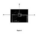
- FIG. 4shows a micrograph of an inductor fabricated using the M 3 DTM process on Kapton target 36 .
- the first layer of silver linesrequires a thickness (at least 10 microns) sufficient to prevent shorting due to electromigration of silver to the ferrite/glass layer during laser sintering of the core.
- the top layer of diagonal silver linesis typically written over a 100-500 micron nonconformal surface (in this case, ferrite core 34 ) to connect the bottom silver lines, forming inductor coil 30 .
- the bottom electrode lines of layer oneare fully dense traces with heights of approximately 50 microns.
- Contact pad 32is 1 mm square.
- Ferrite core 34is a 5 ⁇ 15 mm rectangle with a maximum height of 400 microns, and is preferably formed from a manganese/zinc iron oxide and glass powder.
- the inductance curve of an M 3 DTM-fabricated inductor printed on Kaptonis shown in FIG. 5 , and reveals a gradual and predictable increase from 0.8 to 1.5 microHenrys in the range from 40 Hz to 110 MHz.
- the quality factor or energy stored per cyclewas 50 at 50 MHz.
- the M 3 DTM processhas also been used to fabricate type-S (platinum, platinum/rhodium) thermocouples on tantalum nitride (TaN) targets.
- the platinum side of the devicewas written on the left arm of the thermocouple.
- the targeted alloying ratio of the platinum/rhodium armwas 90% Pt and 10% Rh.
- the deviceswere electrically insulated from the target using an adhesive Kapton film.
- Thin films of platinum (Pt) and platinum/rhodium (Pt/Rh) liquid precursorswere deposited onto an insulating layer of polyimide.
- Laser decompositionwas used to drive the films to the metal state.
- Sample cleaning and surface modificationwas used to clean the Kapton film, and to promote wetting and adhesion of the Pt and Pt/Rh precursors.
- Laser chemical processingachieved electrical properties near that of bulk Pt and Pt/Rh.
- Four-point probe measurementswere used to qualitatively determine the degree of decomposition and porosity. In printing each device, the precursor for one arm was deposited and then laser decomposed. This procedure was then repeated for the remaining arm of the thermocouple. The intersections of the leads that connect the junction to contact pads are of particular interest.
- FIG. 6shows a micrograph of the intersection of a thermocouple junction and the lead wires. The figure shows a smooth transition from Pt-Pt/Rh junction 38 to Pt lead 40 , which was deposited first, and to Pt/Rh (arm) lead 42 , which was deposited over junction 38 . Deposition of metal layers with a thickness of more than a few hundred nanometers may also lead to unacceptable cracking of the decomposed metal film. In this example the deposit thickness is therefore held to approximately 0.2 to 0.5 microns. Metallization requiring greater thickness may be obtained by using an iterative method to deposit and decompose several layers.
- the calibration curve for an M 3 DTM-fabricated thermocoupleis shown in FIG. 7 .
- the corresponding curve for a standard type-S thermocouple with a reference temperature of 0° C.is also shown. Data was taken from 21° C. to 177° C.
- the deviceshows a characteristic curve that is very similar to the standard curve.
- the slope of the experimental curveis within less than 3% of the slope of the standard curve (7.50 ⁇ 10 ⁇ 3 mV/°C. versus 7.73 ⁇ 10 ⁇ 3 mV/°C.) from 65 to 177° C.
- the difference in outputmay be due to the use of a reference temperature of approximately 21° C., rather than 0° C.
- the inventionmay be used for metallization of plastic targets and UV curable polymers (bus lines, electrodes, interconnects, etc.), deposition of passive electronic components onto circuit board, deposition of embedded passives on circuit board, fabrication of vias between target layers, and metallization of epoxies.
- the M 3 DTM processhas been used to deposit and sinter silver on polycarbonate target material.
- an alternate approach to the precursor chemistry methodwas used to reduce the processing temperature required for direct write of metal lines on polycarbonate. This approach entails the use of a nanoparticle silver ink composed of nanometer-sized silver particles suspended in an aqueous solution. The median diameter of the particles was approximately 50 nanometers.
- a nanoparticle formulation to print silver lines onto a low-temperature targetcan be extended to gold, and has the following advantages: the desired material (i.e., a highly conductive metal) already exists, eliminating the need for decomposition and removal of volatile organic solvents; the suspending medium can be aqueous, and will not chemically degrade polycarbonate; good adhesion on plastic has been demonstrated in a previous study; deposition and processing may be accomplished with the target held at room temperature; the nanoparticle ink can be deposited with linewidths below 10 microns; nanometer-size particles sinter at a laser power ( ⁇ 100 mW) that does not damage polycarbonate; and near bulk electrical properties are possible with laser sintering.
- the desired materiali.e., a highly conductive metal
- the suspending mediumcan be aqueous, and will not chemically degrade polycarbonate
- good adhesion on plastichas been demonstrated in a previous study
- deposition and processingmay be accomplished with the target held at room temperature
- FIGS. 8 a and 8 bMicrographs of sintered silver lines on polycarbonate are shown in FIGS. 8 a and 8 b .
- the resistivity of the linesis only about 3 ⁇ the bulk resistivity of silver.
- the sintering temperatureis approximately 180° C., which is significantly higher than the 120° C. damage threshold of polycarbonate.
- a treatable platinum depositionwas prepared from water-soluble platinum tetrachloride. Droplets of platinum tetrachloride were preheated as they enter the deposition apparatus, and the temperature of the deposited material was raised to approximately 580 degrees Celsius via a substrate heater. A low-power diode laser then completed the decomposition of the platinum tetrachloride to pure platinum in the desired pattern.
- preferred laser-treatable materialsinclude but are not limited to: platinum tetrachloride, gold tetrachloride, copper formate, silver acetate, silver nitrate, barium titanate and aluminum oxide.
- the M 3 DTM processhas been used to fabricate Ultra-High Density Interconnects (UHDI).
- UHDIUltra-High Density Interconnects
- the minimum high-density interconnect linewidth attainable using conventional mask photolithographic techniquesis approximately 50 microns, on a 50 to 75 micron pitch (spacing).
- the trend, however, in the HDI circuit industryhas begun to demand low-cost, ultra-high density circuitry; i.e., linewidths from approximately 10 to 40 microns.
- Ink jettinghas been used to deposit conductive lines onto plastic and other low-temperature targets using conductive polymer solutions. This method however yields lines with resistivities that are 10 4 to 10 6 times more resistive than metal lines deposited on plastics using the M 3 DTM technology.
- ink jettingis limited to linewidth of approximately 50 microns.
- the M 3 DTM processhas been used to deposit high-density metal lines with a 25-micron linewidth on a 50-micron pitch. Twenty five micron wide precursor traces were deposited, and laser decomposition was used to define the final linewidth. The un-decomposed precursor was rinsed from the target; it may optionally be reclaimed. The process of deposition followed by laser decomposition has yielded linewidths from approximately 1 to 50 microns. As an example, 25-micron Pt interconnect lines with a 50-micron spacing were written onto 1-mil thick KaptonTM film using the M 3 DTM process. The targeted goal of 10-micron wide Pt lines with 10-micron spacing on polyimide is possible with optimized processing parameters.
- FIG. 9shows silver interconnects deposited on PMMA for a polymer display application. It illustrates the capability of M3D to deposit and laser-fire conductive inks on low temperature polymer. The silver nanoparticle ink was deposited into 35 micron wide lines on the PMMA. The ink was then allowed to dry for 5 minutes at 80° C. After drying, a 50 mW, 532 nm CW laser was focused onto the deposits and scanned at 20 mm/s in order to sinter the nanoparticles. The measured resistance of 6 cm-long interconnects was 100 Ohms. This corresponds to a resistivity of 16 ⁇ Ohm-cm, which is less than approximately 10 ⁇ larger than that of bulk silver. The deposits adhered well to the PMMA, passing an adhesive tape test.
Landscapes
- Engineering & Computer Science (AREA)
- Manufacturing & Machinery (AREA)
- Microelectronics & Electronic Packaging (AREA)
- Physical Vapour Deposition (AREA)
- Other Surface Treatments For Metallic Materials (AREA)
- Manufacturing Of Printed Wiring (AREA)
Abstract
Description
Claims (21)
Priority Applications (1)
| Application Number | Priority Date | Filing Date | Title |
|---|---|---|---|
| US11/430,636US8110247B2 (en) | 1998-09-30 | 2006-05-08 | Laser processing for heat-sensitive mesoscale deposition of oxygen-sensitive materials |
Applications Claiming Priority (15)
| Application Number | Priority Date | Filing Date | Title |
|---|---|---|---|
| US10241898P | 1998-09-30 | 1998-09-30 | |
| US09/305,985US6251488B1 (en) | 1999-05-05 | 1999-05-05 | Precision spray processes for direct write electronic components |
| US40862199A | 1999-09-30 | 1999-09-30 | |
| US09/574,955US6823124B1 (en) | 1998-09-30 | 2000-05-19 | Laser-guided manipulation of non-atomic particles |
| US09/584,997US6636676B1 (en) | 1998-09-30 | 2000-06-01 | Particle guidance system |
| US09/844,666US20020170890A1 (en) | 2001-04-27 | 2001-04-27 | Precision spray processes for direct write electronic components |
| US10/060,960US20030020768A1 (en) | 1998-09-30 | 2002-01-30 | Direct write TM system |
| US10/072,605US7108894B2 (en) | 1998-09-30 | 2002-02-05 | Direct Write™ System |
| US10/346,935US7045015B2 (en) | 1998-09-30 | 2003-01-17 | Apparatuses and method for maskless mesoscale material deposition |
| US50649503P | 2003-09-26 | 2003-09-26 | |
| US50875903P | 2003-10-03 | 2003-10-03 | |
| US10/746,646US20040197493A1 (en) | 1998-09-30 | 2003-12-23 | Apparatus, methods and precision spray processes for direct write and maskless mesoscale material deposition |
| US10/952,108US7294366B2 (en) | 1998-09-30 | 2004-09-27 | Laser processing for heat-sensitive mesoscale deposition |
| US10/952,107US20050156991A1 (en) | 1998-09-30 | 2004-09-27 | Maskless direct write of copper using an annular aerosol jet |
| US11/430,636US8110247B2 (en) | 1998-09-30 | 2006-05-08 | Laser processing for heat-sensitive mesoscale deposition of oxygen-sensitive materials |
Related Parent Applications (3)
| Application Number | Title | Priority Date | Filing Date |
|---|---|---|---|
| US10/746,646Continuation-In-PartUS20040197493A1 (en) | 1998-09-30 | 2003-12-23 | Apparatus, methods and precision spray processes for direct write and maskless mesoscale material deposition |
| US10/952,108Continuation-In-PartUS7294366B2 (en) | 1998-09-30 | 2004-09-27 | Laser processing for heat-sensitive mesoscale deposition |
| US10/952,107Continuation-In-PartUS20050156991A1 (en) | 1998-09-30 | 2004-09-27 | Maskless direct write of copper using an annular aerosol jet |
Related Child Applications (1)
| Application Number | Title | Priority Date | Filing Date |
|---|---|---|---|
| US09/584,997Continuation-In-PartUS6636676B1 (en) | 1998-09-30 | 2000-06-01 | Particle guidance system |
Publications (2)
| Publication Number | Publication Date |
|---|---|
| US20070019028A1 US20070019028A1 (en) | 2007-01-25 |
| US8110247B2true US8110247B2 (en) | 2012-02-07 |
Family
ID=37678650
Family Applications (1)
| Application Number | Title | Priority Date | Filing Date |
|---|---|---|---|
| US11/430,636Expired - Fee RelatedUS8110247B2 (en) | 1998-09-30 | 2006-05-08 | Laser processing for heat-sensitive mesoscale deposition of oxygen-sensitive materials |
Country Status (1)
| Country | Link |
|---|---|
| US (1) | US8110247B2 (en) |
Cited By (14)
| Publication number | Priority date | Publication date | Assignee | Title |
|---|---|---|---|---|
| US9254535B2 (en) | 2014-06-20 | 2016-02-09 | Velo3D, Inc. | Apparatuses, systems and methods for three-dimensional printing |
| US9662840B1 (en) | 2015-11-06 | 2017-05-30 | Velo3D, Inc. | Adept three-dimensional printing |
| US9919360B2 (en) | 2016-02-18 | 2018-03-20 | Velo3D, Inc. | Accurate three-dimensional printing |
| US9962767B2 (en) | 2015-12-10 | 2018-05-08 | Velo3D, Inc. | Apparatuses for three-dimensional printing |
| US20180126649A1 (en) | 2016-11-07 | 2018-05-10 | Velo3D, Inc. | Gas flow in three-dimensional printing |
| US10144176B1 (en) | 2018-01-15 | 2018-12-04 | Velo3D, Inc. | Three-dimensional printing systems and methods of their use |
| US10252336B2 (en) | 2016-06-29 | 2019-04-09 | Velo3D, Inc. | Three-dimensional printing and three-dimensional printers |
| US10272525B1 (en) | 2017-12-27 | 2019-04-30 | Velo3D, Inc. | Three-dimensional printing systems and methods of their use |
| US10315252B2 (en) | 2017-03-02 | 2019-06-11 | Velo3D, Inc. | Three-dimensional printing of three-dimensional objects |
| US10449696B2 (en) | 2017-03-28 | 2019-10-22 | Velo3D, Inc. | Material manipulation in three-dimensional printing |
| US10611092B2 (en) | 2017-01-05 | 2020-04-07 | Velo3D, Inc. | Optics in three-dimensional printing |
| US11691343B2 (en) | 2016-06-29 | 2023-07-04 | Velo3D, Inc. | Three-dimensional printing and three-dimensional printers |
| US11999110B2 (en) | 2019-07-26 | 2024-06-04 | Velo3D, Inc. | Quality assurance in formation of three-dimensional objects |
| US12070907B2 (en) | 2016-09-30 | 2024-08-27 | Velo3D | Three-dimensional objects and their formation |
Families Citing this family (29)
| Publication number | Priority date | Publication date | Assignee | Title |
|---|---|---|---|---|
| US20050156991A1 (en)* | 1998-09-30 | 2005-07-21 | Optomec Design Company | Maskless direct write of copper using an annular aerosol jet |
| US7108894B2 (en)* | 1998-09-30 | 2006-09-19 | Optomec Design Company | Direct Write™ System |
| US7045015B2 (en) | 1998-09-30 | 2006-05-16 | Optomec Design Company | Apparatuses and method for maskless mesoscale material deposition |
| CA2412904A1 (en)* | 2000-06-13 | 2001-12-20 | Element Six (Pty) Ltd. | Composite diamond compacts |
| WO2005094440A2 (en) | 2004-03-18 | 2005-10-13 | Nanosys Inc. | Nanofiber surface based capacitors |
| US7674671B2 (en) | 2004-12-13 | 2010-03-09 | Optomec Design Company | Aerodynamic jetting of aerosolized fluids for fabrication of passive structures |
| US7938341B2 (en)* | 2004-12-13 | 2011-05-10 | Optomec Design Company | Miniature aerosol jet and aerosol jet array |
| WO2006099538A2 (en)* | 2005-03-15 | 2006-09-21 | Nanodynamics, Inc. | Devices with ultrathin structures and method of making same |
| US20070154634A1 (en)* | 2005-12-15 | 2007-07-05 | Optomec Design Company | Method and Apparatus for Low-Temperature Plasma Sintering |
| US20100310630A1 (en)* | 2007-04-27 | 2010-12-09 | Technische Universitat Braunschweig | Coated surface for cell culture |
| US10231344B2 (en)* | 2007-05-18 | 2019-03-12 | Applied Nanotech Holdings, Inc. | Metallic ink |
| TWI482662B (en)* | 2007-08-30 | 2015-05-01 | Optomec Inc | Mechanically integrated and tightly coupled print heads and spray sources |
| TWI538737B (en)* | 2007-08-31 | 2016-06-21 | 阿普托麥克股份有限公司 | Material deposition assembly |
| TW200918325A (en)* | 2007-08-31 | 2009-05-01 | Optomec Inc | AEROSOL JET® printing system for photovoltaic applications |
| US8887658B2 (en)* | 2007-10-09 | 2014-11-18 | Optomec, Inc. | Multiple sheath multiple capillary aerosol jet |
| KR101120743B1 (en)* | 2007-10-22 | 2012-03-22 | 히다치 가세고교 가부시끼가이샤 | Method of forming copper wiring pattern and copper oxide particle dispersion for use in the same |
| FR2957479B1 (en)* | 2010-03-12 | 2012-04-27 | Commissariat Energie Atomique | PROCESS FOR TREATING A METAL CONTACT REALIZED ON A SUBSTRATE |
| US9245573B2 (en) | 2013-06-24 | 2016-01-26 | Seagate Technology Llc | Methods of forming materials for at least a portion of a NFT and NFTs formed using the same |
| US20150132503A1 (en)* | 2013-11-13 | 2015-05-14 | Seagate Technology Llc | Methods of forming near field transducers |
| DE102014101522A1 (en)* | 2014-02-07 | 2015-08-13 | 3D Schilling Gmbh | Method and apparatus for selectively activating at least a portion of a surface of a dielectric substrate |
| US20150225845A1 (en)* | 2014-02-12 | 2015-08-13 | Electronics And Telecommunications Research Institute | Method for forming metal oxide thin film and device for printing metal oxide thin film |
| KR102444204B1 (en) | 2015-02-10 | 2022-09-19 | 옵토멕 인코포레이티드 | Method for manufacturing three-dimensional structures by in-flight curing of aerosols |
| JP6630053B2 (en) | 2015-03-25 | 2020-01-15 | スタンレー電気株式会社 | Electronic device manufacturing method |
| WO2016164729A1 (en)* | 2015-04-08 | 2016-10-13 | President And Fellows Of Harvard College | Inline laser sintering of metallic inks |
| JP6491032B2 (en)* | 2015-04-24 | 2019-03-27 | スタンレー電気株式会社 | Manufacturing method of resistor and resistor |
| CN105773072A (en)* | 2015-12-30 | 2016-07-20 | 北京航科精机科技有限公司 | Method for additive manufacturing of complex metal part through sheet layer overlaying |
| US11164600B1 (en) | 2016-08-26 | 2021-11-02 | Seagate Technology Llc | Methods of forming materials |
| CN111655382B (en) | 2017-11-13 | 2022-05-31 | 奥普托美克公司 | Blocking of aerosol flow |
| TW202247905A (en) | 2021-04-29 | 2022-12-16 | 美商阿普托麥克股份有限公司 | High reliability sheathed transport path for aerosol jet devices |
Citations (175)
| Publication number | Priority date | Publication date | Assignee | Title |
|---|---|---|---|---|
| US3474971A (en) | 1967-06-14 | 1969-10-28 | North American Rockwell | Two-piece injector |
| US3590477A (en) | 1968-12-19 | 1971-07-06 | Ibm | Method for fabricating insulated-gate field effect transistors having controlled operating characeristics |
| US3642202A (en) | 1970-05-13 | 1972-02-15 | Exxon Research Engineering Co | Feed system for coking unit |
| US3715785A (en) | 1971-04-29 | 1973-02-13 | Ibm | Technique for fabricating integrated incandescent displays |
| US3808432A (en) | 1970-06-04 | 1974-04-30 | Bell Telephone Labor Inc | Neutral particle accelerator utilizing radiation pressure |
| US3808550A (en) | 1969-12-15 | 1974-04-30 | Bell Telephone Labor Inc | Apparatuses for trapping and accelerating neutral particles |
| US3846661A (en) | 1971-04-29 | 1974-11-05 | Ibm | Technique for fabricating integrated incandescent displays |
| US3854321A (en) | 1973-04-27 | 1974-12-17 | B Dahneke | Aerosol beam device and method |
| US3901798A (en) | 1973-11-21 | 1975-08-26 | Environmental Research Corp | Aerosol concentrator and classifier |
| US3959798A (en) | 1974-12-31 | 1976-05-25 | International Business Machines Corporation | Selective wetting using a micromist of particles |
| US3974769A (en) | 1975-05-27 | 1976-08-17 | International Business Machines Corporation | Method and apparatus for recording information on a recording surface through the use of mists |
| US3982251A (en) | 1974-08-23 | 1976-09-21 | Ibm Corporation | Method and apparatus for recording information on a recording medium |
| US4016417A (en) | 1976-01-08 | 1977-04-05 | Richard Glasscock Benton | Laser beam transport, and method |
| US4019188A (en) | 1975-05-12 | 1977-04-19 | International Business Machines Corporation | Micromist jet printer |
| US4034025A (en) | 1976-02-09 | 1977-07-05 | Martner John G | Ultrasonic gas stream liquid entrainment apparatus |
| US4046074A (en) | 1976-02-02 | 1977-09-06 | International Business Machines Corporation | Non-impact printing system |
| US4046073A (en) | 1976-01-28 | 1977-09-06 | International Business Machines Corporation | Ultrasonic transfer printing with multi-copy, color and low audible noise capability |
| US4092535A (en) | 1977-04-22 | 1978-05-30 | Bell Telephone Laboratories, Incorporated | Damping of optically levitated particles by feedback and beam shaping |
| US4112437A (en) | 1977-06-27 | 1978-09-05 | Eastman Kodak Company | Electrographic mist development apparatus and method |
| US4132894A (en) | 1978-04-04 | 1979-01-02 | The United States Of America As Represented By The United States Department Of Energy | Monitor of the concentration of particles of dense radioactive materials in a stream of air |
| US4171096A (en) | 1977-05-26 | 1979-10-16 | John Welsh | Spray gun nozzle attachment |
| US4200669A (en) | 1978-11-22 | 1980-04-29 | The United States Of America As Represented By The Secretary Of The Navy | Laser spraying |
| US4228440A (en) | 1977-12-22 | 1980-10-14 | Ricoh Company, Ltd. | Ink jet printing apparatus |
| US4269868A (en)* | 1979-03-30 | 1981-05-26 | Rolls-Royce Limited | Application of metallic coatings to metallic substrates |
| US4323756A (en) | 1979-10-29 | 1982-04-06 | United Technologies Corporation | Method for fabricating articles by sequential layer deposition |
| US4453803A (en) | 1981-06-25 | 1984-06-12 | Agency Of Industrial Science & Technology | Optical waveguide for middle infrared band |
| US4485387A (en) | 1982-10-26 | 1984-11-27 | Microscience Systems Corp. | Inking system for producing circuit patterns |
| US4497692A (en) | 1983-06-13 | 1985-02-05 | International Business Machines Corporation | Laser-enhanced jet-plating and jet-etching: high-speed maskless patterning method |
| US4601921A (en) | 1984-12-24 | 1986-07-22 | General Motors Corporation | Method and apparatus for spraying coating material |
| US4605574A (en) | 1981-09-14 | 1986-08-12 | Takashi Yonehara | Method and apparatus for forming an extremely thin film on the surface of an object |
| US4670135A (en) | 1986-06-27 | 1987-06-02 | Regents Of The University Of Minnesota | High volume virtual impactor |
| US4689052A (en) | 1986-02-19 | 1987-08-25 | Washington Research Foundation | Virtual impactor |
| US4825299A (en) | 1986-08-29 | 1989-04-25 | Hitachi, Ltd. | Magnetic recording/reproducing apparatus utilizing phase comparator |
| US4826583A (en) | 1986-09-25 | 1989-05-02 | Lasers Applications Belgium, En Abrege Label S.A. | Apparatus for pinpoint laser-assisted electroplating of metals on solid substrates |
| EP0331022A2 (en) | 1988-03-01 | 1989-09-06 | Texas Instruments Incorporated | Radiation induced pattern deposition |
| US4893886A (en) | 1987-09-17 | 1990-01-16 | American Telephone And Telegraph Company | Non-destructive optical trap for biological particles and method of doing same |
| US4904621A (en) | 1987-07-16 | 1990-02-27 | Texas Instruments Incorporated | Remote plasma generation process using a two-stage showerhead |
| US4911365A (en) | 1989-01-26 | 1990-03-27 | James E. Hynds | Spray gun having a fanning air turbine mechanism |
| US4920254A (en) | 1988-02-22 | 1990-04-24 | Sierracin Corporation | Electrically conductive window and a method for its manufacture |
| US4947463A (en) | 1988-02-24 | 1990-08-07 | Agency Of Industrial Science & Technology | Laser spraying process |
| US4971251A (en) | 1988-11-28 | 1990-11-20 | Minnesota Mining And Manufacturing Company | Spray gun with disposable liquid handling portion |
| US4997809A (en) | 1987-11-18 | 1991-03-05 | International Business Machines Corporation | Fabrication of patterned lines of high Tc superconductors |
| US5032850A (en) | 1989-12-18 | 1991-07-16 | Tokyo Electric Co., Ltd. | Method and apparatus for vapor jet printing |
| US5043548A (en) | 1989-02-08 | 1991-08-27 | General Electric Company | Axial flow laser plasma spraying |
| EP0444550A2 (en) | 1990-03-02 | 1991-09-04 | Fried. Krupp AG Hoesch-Krupp | Apparatus for supplying powder filler materials in a welding zone |
| US5064685A (en) | 1989-08-23 | 1991-11-12 | At&T Laboratories | Electrical conductor deposition method |
| US5164535A (en) | 1991-09-05 | 1992-11-17 | Silent Options, Inc. | Gun silencer |
| US5170890A (en) | 1990-12-05 | 1992-12-15 | Wilson Steven D | Particle trap |
| US5176744A (en)* | 1991-08-09 | 1993-01-05 | Microelectronics Computer & Technology Corp. | Solution for direct copper writing |
| US5182430A (en) | 1990-10-10 | 1993-01-26 | Societe National D'etude Et De Construction De Moteurs D'aviation "S.N.E.C.M.A." | Powder supply device for the formation of coatings by laser beam treatment |
| US5194297A (en) | 1992-03-04 | 1993-03-16 | Vlsi Standards, Inc. | System and method for accurately depositing particles on a surface |
| US5208431A (en) | 1990-09-10 | 1993-05-04 | Agency Of Industrial Science & Technology | Method for producing object by laser spraying and apparatus for conducting the method |
| US5245404A (en) | 1990-10-18 | 1993-09-14 | Physical Optics Corportion | Raman sensor |
| US5250383A (en) | 1990-02-23 | 1993-10-05 | Fuji Photo Film Co., Ltd. | Process for forming multilayer coating |
| US5254832A (en) | 1990-01-12 | 1993-10-19 | U.S. Philips Corporation | Method of manufacturing ultrafine particles and their application |
| US5270542A (en)* | 1992-12-31 | 1993-12-14 | Regents Of The University Of Minnesota | Apparatus and method for shaping and detecting a particle beam |
| US5292418A (en) | 1991-03-08 | 1994-03-08 | Mitsubishi Denki Kabushiki Kaisha | Local laser plating apparatus |
| US5322221A (en) | 1992-11-09 | 1994-06-21 | Graco Inc. | Air nozzle |
| EP0470911B1 (en) | 1990-08-10 | 1994-07-27 | Roussel-Uclaf | Spraying system |
| US5335000A (en) | 1992-08-04 | 1994-08-02 | Calcomp Inc. | Ink vapor aerosol pen for pen plotters |
| US5344676A (en) | 1992-10-23 | 1994-09-06 | The Board Of Trustees Of The University Of Illinois | Method and apparatus for producing nanodrops and nanoparticles and thin film deposits therefrom |
| US5366559A (en) | 1993-05-27 | 1994-11-22 | Research Triangle Institute | Method for protecting a substrate surface from contamination using the photophoretic effect |
| US5378505A (en) | 1991-02-27 | 1995-01-03 | Honda Giken Kogyo Kabushiki Kaisha | Method of and apparatus for electrostatically spray-coating work with paint |
| US5378508A (en) | 1992-04-01 | 1995-01-03 | Akzo Nobel N.V. | Laser direct writing |
| US5403617A (en) | 1993-09-15 | 1995-04-04 | Mobium Enterprises Corporation | Hybrid pulsed valve for thin film coating and method |
| US5449536A (en) | 1992-12-18 | 1995-09-12 | United Technologies Corporation | Method for the application of coatings of oxide dispersion strengthened metals by laser powder injection |
| US5486676A (en) | 1994-11-14 | 1996-01-23 | General Electric Company | Coaxial single point powder feed nozzle |
| US5495105A (en) | 1992-02-20 | 1996-02-27 | Canon Kabushiki Kaisha | Method and apparatus for particle manipulation, and measuring apparatus utilizing the same |
| US5512745A (en) | 1994-03-09 | 1996-04-30 | Board Of Trustees Of The Leland Stanford Jr. University | Optical trap system and method |
| US5607730A (en) | 1995-09-11 | 1997-03-04 | Clover Industries, Inc. | Method and apparatus for laser coating |
| US5609921A (en) | 1994-08-26 | 1997-03-11 | Universite De Sherbrooke | Suspension plasma spray |
| US5612099A (en) | 1995-05-23 | 1997-03-18 | Mcdonnell Douglas Corporation | Method and apparatus for coating a substrate |
| US5614252A (en) | 1988-12-27 | 1997-03-25 | Symetrix Corporation | Method of fabricating barium strontium titanate |
| US5648127A (en) | 1994-01-18 | 1997-07-15 | Qqc, Inc. | Method of applying, sculpting, and texturing a coating on a substrate and for forming a heteroepitaxial coating on a surface of a substrate |
| US5676719A (en) | 1996-02-01 | 1997-10-14 | Engineering Resources, Inc. | Universal insert for use with radiator steam traps |
| US5733609A (en) | 1993-06-01 | 1998-03-31 | Wang; Liang | Ceramic coatings synthesized by chemical reactions energized by laser plasmas |
| US5736195A (en) | 1993-09-15 | 1998-04-07 | Mobium Enterprises Corporation | Method of coating a thin film on a substrate |
| US5742050A (en) | 1996-09-30 | 1998-04-21 | Aviv Amirav | Method and apparatus for sample introduction into a mass spectrometer for improving a sample analysis |
| US5770272A (en) | 1995-04-28 | 1998-06-23 | Massachusetts Institute Of Technology | Matrix-bearing targets for maldi mass spectrometry and methods of production thereof |
| US5772106A (en) | 1995-12-29 | 1998-06-30 | Microfab Technologies, Inc. | Printhead for liquid metals and method of use |
| US5814152A (en) | 1995-05-23 | 1998-09-29 | Mcdonnell Douglas Corporation | Apparatus for coating a substrate |
| US5844192A (en) | 1996-05-09 | 1998-12-01 | United Technologies Corporation | Thermal spray coating method and apparatus |
| US5854311A (en) | 1996-06-24 | 1998-12-29 | Richart; Douglas S. | Process and apparatus for the preparation of fine powders |
| US5861136A (en)* | 1995-01-10 | 1999-01-19 | E. I. Du Pont De Nemours And Company | Method for making copper I oxide powders by aerosol decomposition |
| US5882722A (en) | 1995-07-12 | 1999-03-16 | Partnerships Limited, Inc. | Electrical conductors formed from mixtures of metal powders and metallo-organic decompositions compounds |
| US5894403A (en) | 1997-05-01 | 1999-04-13 | Wilson Greatbatch Ltd. | Ultrasonically coated substrate for use in a capacitor |
| US5940099A (en) | 1993-08-15 | 1999-08-17 | Ink Jet Technology, Inc. & Scitex Corporation Ltd. | Ink jet print head with ink supply through porous medium |
| US5958268A (en) | 1995-06-07 | 1999-09-28 | Cauldron Limited Partnership | Removal of material by polarized radiation |
| US5965212A (en) | 1995-07-27 | 1999-10-12 | Isis Innovation Limited | Method of producing metal quantum dots |
| US5980998A (en) | 1997-09-16 | 1999-11-09 | Sri International | Deposition of substances on a surface |
| US5993549A (en) | 1996-01-19 | 1999-11-30 | Deutsche Forschungsanstalt Fuer Luft- Und Raumfahrt E.V. | Powder coating apparatus |
| US5997956A (en) | 1995-08-04 | 1999-12-07 | Microcoating Technologies | Chemical vapor deposition and powder formation using thermal spray with near supercritical and supercritical fluid solutions |
| US6007631A (en) | 1997-11-10 | 1999-12-28 | Speedline Technologies, Inc. | Multiple head dispensing system and method |
| US6015083A (en) | 1995-12-29 | 2000-01-18 | Microfab Technologies, Inc. | Direct solder bumping of hard to solder substrate |
| US6025037A (en) | 1994-04-25 | 2000-02-15 | U.S. Philips Corporation | Method of curing a film |
| US6110144A (en) | 1998-01-15 | 2000-08-29 | Medtronic Ave, Inc. | Method and apparatus for regulating the fluid flow rate to and preventing over-pressurization of a balloon catheter |
| US6116718A (en) | 1998-09-30 | 2000-09-12 | Xerox Corporation | Print head for use in a ballistic aerosol marking apparatus |
| US6136442A (en) | 1998-09-30 | 2000-10-24 | Xerox Corporation | Multi-layer organic overcoat for particulate transport electrode grid |
| US6151435A (en) | 1998-11-01 | 2000-11-21 | The United States Of America As Represented By The Secretary Of The Navy | Evanescent atom guiding in metal-coated hollow-core optical fibers |
| US6159749A (en) | 1998-07-21 | 2000-12-12 | Beckman Coulter, Inc. | Highly sensitive bead-based multi-analyte assay system using optical tweezers |
| US6182688B1 (en) | 1998-06-19 | 2001-02-06 | Aerospatiale Societe Nationale Industrielle | Autonomous device for limiting the rate of flow of a fluid through a pipe, and fuel circuit for an aircraft comprising such a device |
| US6197366B1 (en) | 1997-05-06 | 2001-03-06 | Takamatsu Research Laboratory | Metal paste and production process of metal film |
| US6251488B1 (en) | 1999-05-05 | 2001-06-26 | Optomec Design Company | Precision spray processes for direct write electronic components |
| US6258733B1 (en) | 1996-05-21 | 2001-07-10 | Sand Hill Capital Ii, Lp | Method and apparatus for misted liquid source deposition of thin film with reduced mist particle size |
| US6265050B1 (en) | 1998-09-30 | 2001-07-24 | Xerox Corporation | Organic overcoat for electrode grid |
| US6267301B1 (en) | 1999-06-11 | 2001-07-31 | Spraying Systems Co. | Air atomizing nozzle assembly with improved air cap |
| US6290342B1 (en) | 1998-09-30 | 2001-09-18 | Xerox Corporation | Particulate marking material transport apparatus utilizing traveling electrostatic waves |
| US6291088B1 (en) | 1998-09-30 | 2001-09-18 | Xerox Corporation | Inorganic overcoat for particulate transport electrode grid |
| US6293659B1 (en) | 1999-09-30 | 2001-09-25 | Xerox Corporation | Particulate source, circulation, and valving system for ballistic aerosol marking |
| US20010046551A1 (en) | 2000-02-16 | 2001-11-29 | Michael Falck | Strip coating method |
| US6340216B1 (en) | 1998-09-30 | 2002-01-22 | Xerox Corporation | Ballistic aerosol marking apparatus for treating a substrate |
| US20020012743A1 (en) | 2000-07-25 | 2002-01-31 | The Research Foundation Of State University Of New York | Method and apparatus for fine feature spray deposition |
| US6348687B1 (en) | 1999-09-10 | 2002-02-19 | Sandia Corporation | Aerodynamic beam generator for large particles |
| US6349668B1 (en) | 1998-04-27 | 2002-02-26 | Msp Corporation | Method and apparatus for thin film deposition on large area substrates |
| US6379745B1 (en) | 1997-02-20 | 2002-04-30 | Parelec, Inc. | Low temperature method and compositions for producing electrical conductors |
| US6384365B1 (en) | 2000-04-14 | 2002-05-07 | Siemens Westinghouse Power Corporation | Repair and fabrication of combustion turbine components by spark plasma sintering |
| US6390115B1 (en) | 1998-05-20 | 2002-05-21 | GSF-Forschungszentrum für Umwelt und Gesundheit | Method and device for producing a directed gas jet |
| US20020063117A1 (en)* | 2000-04-19 | 2002-05-30 | Church Kenneth H. | Laser sintering of materials and a thermal barrier for protecting a substrate |
| US6406137B1 (en) | 1998-12-22 | 2002-06-18 | Canon Kabushiki Kaisha | Ink-jet print head and production method of ink-jet print head |
| US6416159B1 (en) | 1998-09-30 | 2002-07-09 | Xerox Corporation | Ballistic aerosol marking apparatus with non-wetting coating |
| US6416157B1 (en) | 1998-09-30 | 2002-07-09 | Xerox Corporation | Method of marking a substrate employing a ballistic aerosol marking apparatus |
| US6416389B1 (en) | 2000-07-28 | 2002-07-09 | Xerox Corporation | Process for roughening a surface |
| US6416156B1 (en) | 1998-09-30 | 2002-07-09 | Xerox Corporation | Kinetic fusing of a marking material |
| US20020096647A1 (en) | 2000-08-25 | 2002-07-25 | Asm Lithography B.V. | Mask handling apparatus, lithographic projection apparatus, device manufacturing method and device manufactured thereby |
| US20020100416A1 (en) | 2001-01-30 | 2002-08-01 | Sun James J. | Method and apparatus for deposition of particles on surfaces |
| US20020132051A1 (en) | 1995-12-14 | 2002-09-19 | Kwang-Leong Choy | Film or coating deposition and powder formation |
| US6454384B1 (en) | 1998-09-30 | 2002-09-24 | Xerox Corporation | Method for marking with a liquid material using a ballistic aerosol marking apparatus |
| US6467862B1 (en) | 1998-09-30 | 2002-10-22 | Xerox Corporation | Cartridge for use in a ballistic aerosol marking apparatus |
| US6471327B2 (en) | 2001-02-27 | 2002-10-29 | Eastman Kodak Company | Apparatus and method of delivering a focused beam of a thermodynamically stable/metastable mixture of a functional material in a dense fluid onto a receiver |
| US20020162974A1 (en) | 2001-05-03 | 2002-11-07 | Orsini Rocco A. | High temperature EUV source nozzle |
| US20030003241A1 (en) | 2001-06-27 | 2003-01-02 | Matsushita Electric Industrial Co., Ltd. | Depositing method and a surface modifying method for nano-particles in a gas stream |
| US6503831B2 (en) | 1997-10-14 | 2003-01-07 | Patterning Technologies Limited | Method of forming an electronic device |
| US20030020768A1 (en) | 1998-09-30 | 2003-01-30 | Renn Michael J. | Direct write TM system |
| US6513736B1 (en) | 1996-07-08 | 2003-02-04 | Corning Incorporated | Gas-assisted atomizing device and methods of making gas-assisted atomizing devices |
| US6521297B2 (en) | 2000-06-01 | 2003-02-18 | Xerox Corporation | Marking material and ballistic aerosol marking process for the use thereof |
| US20030048314A1 (en) | 1998-09-30 | 2003-03-13 | Optomec Design Company | Direct write TM system |
| US6537501B1 (en) | 1998-05-18 | 2003-03-25 | University Of Washington | Disposable hematology cartridge |
| US6544599B1 (en) | 1996-07-31 | 2003-04-08 | Univ Arkansas | Process and apparatus for applying charged particles to a substrate, process for forming a layer on a substrate, products made therefrom |
| US6548122B1 (en) | 1997-09-16 | 2003-04-15 | Sri International | Method of producing and depositing a metal film |
| US6573491B1 (en) | 1999-05-17 | 2003-06-03 | Rock Mountain Biosystems, Inc. | Electromagnetic energy driven separation methods |
| US20030108664A1 (en) | 2001-10-05 | 2003-06-12 | Kodas Toivo T. | Methods and compositions for the formation of recessed electrical features on a substrate |
| US20030108511A1 (en) | 1998-08-14 | 2003-06-12 | Sawhney Amarpreet S. | Adhesion barriers applicable by minimally invasive surgery and methods of use thereof |
| US20030117691A1 (en) | 2001-12-21 | 2003-06-26 | Xiangxin Bi | Three dimensional engineering of planar optical structures |
| US20030138967A1 (en) | 2002-01-22 | 2003-07-24 | Dakocytomation Denmark A/S | Environmental containment system for a flow cytometer |
| US20030175411A1 (en) | 2001-10-05 | 2003-09-18 | Kodas Toivo T. | Precursor compositions and methods for the deposition of passive electrical components on a substrate |
| US20030180451A1 (en) | 2001-10-05 | 2003-09-25 | Kodas Toivo T. | Low viscosity copper precursor compositions and methods for the deposition of conductive electronic features |
| US6636676B1 (en) | 1998-09-30 | 2003-10-21 | Optomec Design Company | Particle guidance system |
| US20030202043A1 (en) | 2002-04-24 | 2003-10-30 | Huanzhao Zeng | Determination of control points for construction of first color space-to-second color space look-up table |
| US6646253B1 (en) | 1998-05-20 | 2003-11-11 | GSF-Forschungszentrum für Umwelt und Gesundheit GmbH | Gas inlet for an ion source |
| US20030219923A1 (en) | 2002-03-01 | 2003-11-27 | Arokia Nathan | Method and system for fabricating electronics |
| US20030228124A1 (en) | 1998-09-30 | 2003-12-11 | Renn Michael J. | Apparatuses and method for maskless mesoscale material deposition |
| US20040029706A1 (en) | 2002-02-14 | 2004-02-12 | Barrera Enrique V. | Fabrication of reinforced composite material comprising carbon nanotubes, fullerenes, and vapor-grown carbon fibers for thermal barrier materials, structural ceramics, and multifunctional nanocomposite ceramics |
| US20040038808A1 (en) | 1998-08-27 | 2004-02-26 | Hampden-Smith Mark J. | Method of producing membrane electrode assemblies for use in proton exchange membrane and direct methanol fuel cells |
| US20040080917A1 (en) | 2002-10-23 | 2004-04-29 | Steddom Clark Morrison | Integrated microwave package and the process for making the same |
| US20040151978A1 (en) | 2003-01-30 | 2004-08-05 | Huang Wen C. | Method and apparatus for direct-write of functional materials with a controlled orientation |
| US6772649B2 (en) | 1999-03-25 | 2004-08-10 | GSF-Forschaungszenfrum für Umwelt und Gesundheit GmbH | Gas inlet for reducing a directional and cooled gas jet |
| US20040197493A1 (en) | 1998-09-30 | 2004-10-07 | Optomec Design Company | Apparatus, methods and precision spray processes for direct write and maskless mesoscale material deposition |
| US6811805B2 (en) | 2001-05-30 | 2004-11-02 | Novatis Ag | Method for applying a coating |
| US6823124B1 (en) | 1998-09-30 | 2004-11-23 | Optomec Design Company | Laser-guided manipulation of non-atomic particles |
| US20040247782A1 (en) | 1997-02-24 | 2004-12-09 | Hampden-Smith Mark J. | Palladium-containing particles, method and apparatus of manufacture, palladium-containing devices made therefrom |
| US20050002818A1 (en) | 2003-07-04 | 2005-01-06 | Hitachi Powdered Metals Co., Ltd. | Production method for sintered metal-ceramic layered compact and production method for thermal stress relief pad |
| US6890624B1 (en) | 2000-04-25 | 2005-05-10 | Nanogram Corporation | Self-assembled structures |
| US20050110064A1 (en) | 2002-09-30 | 2005-05-26 | Nanosys, Inc. | Large-area nanoenabled macroelectronic substrates and uses therefor |
| US20050129383A1 (en) | 1998-09-30 | 2005-06-16 | Optomec Design Company | Laser processing for heat-sensitive mesoscale deposition |
| US20050145968A1 (en) | 2003-11-06 | 2005-07-07 | Rohm And Haas Electronic Materials, L.L.C. | Optical article |
| US20050147749A1 (en) | 2004-01-05 | 2005-07-07 | Msp Corporation | High-performance vaporizer for liquid-precursor and multi-liquid-precursor vaporization in semiconductor thin film deposition |
| US20050156991A1 (en) | 1998-09-30 | 2005-07-21 | Optomec Design Company | Maskless direct write of copper using an annular aerosol jet |
| US20050184328A1 (en) | 2004-02-19 | 2005-08-25 | Matsushita Electric Industrial Co., Ltd. | Semiconductor device and its manufacturing method |
| US20060008590A1 (en) | 1998-09-30 | 2006-01-12 | Optomec Design Company | Annular aerosol jet deposition using an extended nozzle |
| US6998785B1 (en) | 2001-07-13 | 2006-02-14 | University Of Central Florida Research Foundation, Inc. | Liquid-jet/liquid droplet initiated plasma discharge for generating useful plasma radiation |
| US20060057014A1 (en) | 2002-09-11 | 2006-03-16 | Nikko Materials Co., Ltd. | Iron silicide sputtering target and method for production thereof |
| WO2006065978A2 (en) | 2004-12-13 | 2006-06-22 | Optomec Design Company | Miniature aerosol jet and aerosol jet array |
| US20060163570A1 (en) | 2004-12-13 | 2006-07-27 | Optomec Design Company | Aerodynamic jetting of aerosolized fluids for fabrication of passive structures |
| US20060172073A1 (en) | 2005-02-01 | 2006-08-03 | Groza Joanna R | Methods for production of FGM net shaped body for various applications |
| JP2007507114A (en) | 2003-09-26 | 2007-03-22 | オプトメック・デザイン・カンパニー | Laser treatment of heat sensitive medium scale deposition. |
Family Cites Families (2)
| Publication number | Priority date | Publication date | Assignee | Title |
|---|---|---|---|---|
| US4200660A (en)* | 1966-04-18 | 1980-04-29 | Firmenich & Cie. | Aromatic sulfur flavoring agents |
| WO1993014022A1 (en)* | 1992-01-15 | 1993-07-22 | Battelle Memorial Institute | Process of forming metal compounds using reverse micelle or reverse microemulsion systems |
- 2006
- 2006-05-08USUS11/430,636patent/US8110247B2/ennot_activeExpired - Fee Related
Patent Citations (190)
| Publication number | Priority date | Publication date | Assignee | Title |
|---|---|---|---|---|
| US3474971A (en) | 1967-06-14 | 1969-10-28 | North American Rockwell | Two-piece injector |
| US3590477A (en) | 1968-12-19 | 1971-07-06 | Ibm | Method for fabricating insulated-gate field effect transistors having controlled operating characeristics |
| US3808550A (en) | 1969-12-15 | 1974-04-30 | Bell Telephone Labor Inc | Apparatuses for trapping and accelerating neutral particles |
| US3642202A (en) | 1970-05-13 | 1972-02-15 | Exxon Research Engineering Co | Feed system for coking unit |
| US3808432A (en) | 1970-06-04 | 1974-04-30 | Bell Telephone Labor Inc | Neutral particle accelerator utilizing radiation pressure |
| US3715785A (en) | 1971-04-29 | 1973-02-13 | Ibm | Technique for fabricating integrated incandescent displays |
| US3846661A (en) | 1971-04-29 | 1974-11-05 | Ibm | Technique for fabricating integrated incandescent displays |
| US3854321A (en) | 1973-04-27 | 1974-12-17 | B Dahneke | Aerosol beam device and method |
| US3901798A (en) | 1973-11-21 | 1975-08-26 | Environmental Research Corp | Aerosol concentrator and classifier |
| US3982251A (en) | 1974-08-23 | 1976-09-21 | Ibm Corporation | Method and apparatus for recording information on a recording medium |
| US3959798A (en) | 1974-12-31 | 1976-05-25 | International Business Machines Corporation | Selective wetting using a micromist of particles |
| US4019188A (en) | 1975-05-12 | 1977-04-19 | International Business Machines Corporation | Micromist jet printer |
| US3974769A (en) | 1975-05-27 | 1976-08-17 | International Business Machines Corporation | Method and apparatus for recording information on a recording surface through the use of mists |
| US4016417A (en) | 1976-01-08 | 1977-04-05 | Richard Glasscock Benton | Laser beam transport, and method |
| US4046073A (en) | 1976-01-28 | 1977-09-06 | International Business Machines Corporation | Ultrasonic transfer printing with multi-copy, color and low audible noise capability |
| US4046074A (en) | 1976-02-02 | 1977-09-06 | International Business Machines Corporation | Non-impact printing system |
| US4034025A (en) | 1976-02-09 | 1977-07-05 | Martner John G | Ultrasonic gas stream liquid entrainment apparatus |
| US4092535A (en) | 1977-04-22 | 1978-05-30 | Bell Telephone Laboratories, Incorporated | Damping of optically levitated particles by feedback and beam shaping |
| US4171096A (en) | 1977-05-26 | 1979-10-16 | John Welsh | Spray gun nozzle attachment |
| US4112437A (en) | 1977-06-27 | 1978-09-05 | Eastman Kodak Company | Electrographic mist development apparatus and method |
| US4228440A (en) | 1977-12-22 | 1980-10-14 | Ricoh Company, Ltd. | Ink jet printing apparatus |
| US4132894A (en) | 1978-04-04 | 1979-01-02 | The United States Of America As Represented By The United States Department Of Energy | Monitor of the concentration of particles of dense radioactive materials in a stream of air |
| US4200669A (en) | 1978-11-22 | 1980-04-29 | The United States Of America As Represented By The Secretary Of The Navy | Laser spraying |
| US4269868A (en)* | 1979-03-30 | 1981-05-26 | Rolls-Royce Limited | Application of metallic coatings to metallic substrates |
| US4323756A (en) | 1979-10-29 | 1982-04-06 | United Technologies Corporation | Method for fabricating articles by sequential layer deposition |
| US4453803A (en) | 1981-06-25 | 1984-06-12 | Agency Of Industrial Science & Technology | Optical waveguide for middle infrared band |
| US4605574A (en) | 1981-09-14 | 1986-08-12 | Takashi Yonehara | Method and apparatus for forming an extremely thin film on the surface of an object |
| US4485387A (en) | 1982-10-26 | 1984-11-27 | Microscience Systems Corp. | Inking system for producing circuit patterns |
| US4497692A (en) | 1983-06-13 | 1985-02-05 | International Business Machines Corporation | Laser-enhanced jet-plating and jet-etching: high-speed maskless patterning method |
| US4601921A (en) | 1984-12-24 | 1986-07-22 | General Motors Corporation | Method and apparatus for spraying coating material |
| US4689052A (en) | 1986-02-19 | 1987-08-25 | Washington Research Foundation | Virtual impactor |
| US4670135A (en) | 1986-06-27 | 1987-06-02 | Regents Of The University Of Minnesota | High volume virtual impactor |
| US4825299A (en) | 1986-08-29 | 1989-04-25 | Hitachi, Ltd. | Magnetic recording/reproducing apparatus utilizing phase comparator |
| US4826583A (en) | 1986-09-25 | 1989-05-02 | Lasers Applications Belgium, En Abrege Label S.A. | Apparatus for pinpoint laser-assisted electroplating of metals on solid substrates |
| US4904621A (en) | 1987-07-16 | 1990-02-27 | Texas Instruments Incorporated | Remote plasma generation process using a two-stage showerhead |
| US4893886A (en) | 1987-09-17 | 1990-01-16 | American Telephone And Telegraph Company | Non-destructive optical trap for biological particles and method of doing same |
| US4997809A (en) | 1987-11-18 | 1991-03-05 | International Business Machines Corporation | Fabrication of patterned lines of high Tc superconductors |
| US4920254A (en) | 1988-02-22 | 1990-04-24 | Sierracin Corporation | Electrically conductive window and a method for its manufacture |
| US4947463A (en) | 1988-02-24 | 1990-08-07 | Agency Of Industrial Science & Technology | Laser spraying process |
| EP0331022A2 (en) | 1988-03-01 | 1989-09-06 | Texas Instruments Incorporated | Radiation induced pattern deposition |
| US4971251A (en) | 1988-11-28 | 1990-11-20 | Minnesota Mining And Manufacturing Company | Spray gun with disposable liquid handling portion |
| US5614252A (en) | 1988-12-27 | 1997-03-25 | Symetrix Corporation | Method of fabricating barium strontium titanate |
| US4911365A (en) | 1989-01-26 | 1990-03-27 | James E. Hynds | Spray gun having a fanning air turbine mechanism |
| US5043548A (en) | 1989-02-08 | 1991-08-27 | General Electric Company | Axial flow laser plasma spraying |
| US5064685A (en) | 1989-08-23 | 1991-11-12 | At&T Laboratories | Electrical conductor deposition method |
| US5032850A (en) | 1989-12-18 | 1991-07-16 | Tokyo Electric Co., Ltd. | Method and apparatus for vapor jet printing |
| US5254832A (en) | 1990-01-12 | 1993-10-19 | U.S. Philips Corporation | Method of manufacturing ultrafine particles and their application |
| US5250383A (en) | 1990-02-23 | 1993-10-05 | Fuji Photo Film Co., Ltd. | Process for forming multilayer coating |
| EP0444550A2 (en) | 1990-03-02 | 1991-09-04 | Fried. Krupp AG Hoesch-Krupp | Apparatus for supplying powder filler materials in a welding zone |
| EP0470911B1 (en) | 1990-08-10 | 1994-07-27 | Roussel-Uclaf | Spraying system |
| US5208431A (en) | 1990-09-10 | 1993-05-04 | Agency Of Industrial Science & Technology | Method for producing object by laser spraying and apparatus for conducting the method |
| US5182430A (en) | 1990-10-10 | 1993-01-26 | Societe National D'etude Et De Construction De Moteurs D'aviation "S.N.E.C.M.A." | Powder supply device for the formation of coatings by laser beam treatment |
| US5245404A (en) | 1990-10-18 | 1993-09-14 | Physical Optics Corportion | Raman sensor |
| US5170890A (en) | 1990-12-05 | 1992-12-15 | Wilson Steven D | Particle trap |
| US5378505A (en) | 1991-02-27 | 1995-01-03 | Honda Giken Kogyo Kabushiki Kaisha | Method of and apparatus for electrostatically spray-coating work with paint |
| US5292418A (en) | 1991-03-08 | 1994-03-08 | Mitsubishi Denki Kabushiki Kaisha | Local laser plating apparatus |
| US5176744A (en)* | 1991-08-09 | 1993-01-05 | Microelectronics Computer & Technology Corp. | Solution for direct copper writing |
| US5164535A (en) | 1991-09-05 | 1992-11-17 | Silent Options, Inc. | Gun silencer |
| US5495105A (en) | 1992-02-20 | 1996-02-27 | Canon Kabushiki Kaisha | Method and apparatus for particle manipulation, and measuring apparatus utilizing the same |
| US5194297A (en) | 1992-03-04 | 1993-03-16 | Vlsi Standards, Inc. | System and method for accurately depositing particles on a surface |
| US5378508A (en) | 1992-04-01 | 1995-01-03 | Akzo Nobel N.V. | Laser direct writing |
| US5335000A (en) | 1992-08-04 | 1994-08-02 | Calcomp Inc. | Ink vapor aerosol pen for pen plotters |
| US5344676A (en) | 1992-10-23 | 1994-09-06 | The Board Of Trustees Of The University Of Illinois | Method and apparatus for producing nanodrops and nanoparticles and thin film deposits therefrom |
| US5322221A (en) | 1992-11-09 | 1994-06-21 | Graco Inc. | Air nozzle |
| US5449536A (en) | 1992-12-18 | 1995-09-12 | United Technologies Corporation | Method for the application of coatings of oxide dispersion strengthened metals by laser powder injection |
| US5270542A (en)* | 1992-12-31 | 1993-12-14 | Regents Of The University Of Minnesota | Apparatus and method for shaping and detecting a particle beam |
| US5366559A (en) | 1993-05-27 | 1994-11-22 | Research Triangle Institute | Method for protecting a substrate surface from contamination using the photophoretic effect |
| US5733609A (en) | 1993-06-01 | 1998-03-31 | Wang; Liang | Ceramic coatings synthesized by chemical reactions energized by laser plasmas |
| US5940099A (en) | 1993-08-15 | 1999-08-17 | Ink Jet Technology, Inc. & Scitex Corporation Ltd. | Ink jet print head with ink supply through porous medium |
| US6481074B1 (en) | 1993-08-15 | 2002-11-19 | Aprion Digital Ltd. | Method of producing an ink jet print head |
| US5403617A (en) | 1993-09-15 | 1995-04-04 | Mobium Enterprises Corporation | Hybrid pulsed valve for thin film coating and method |
| US5736195A (en) | 1993-09-15 | 1998-04-07 | Mobium Enterprises Corporation | Method of coating a thin film on a substrate |
| US5648127A (en) | 1994-01-18 | 1997-07-15 | Qqc, Inc. | Method of applying, sculpting, and texturing a coating on a substrate and for forming a heteroepitaxial coating on a surface of a substrate |
| US5512745A (en) | 1994-03-09 | 1996-04-30 | Board Of Trustees Of The Leland Stanford Jr. University | Optical trap system and method |
| US6025037A (en) | 1994-04-25 | 2000-02-15 | U.S. Philips Corporation | Method of curing a film |
| US5609921A (en) | 1994-08-26 | 1997-03-11 | Universite De Sherbrooke | Suspension plasma spray |
| US5486676A (en) | 1994-11-14 | 1996-01-23 | General Electric Company | Coaxial single point powder feed nozzle |
| US5861136A (en)* | 1995-01-10 | 1999-01-19 | E. I. Du Pont De Nemours And Company | Method for making copper I oxide powders by aerosol decomposition |
| US5770272A (en) | 1995-04-28 | 1998-06-23 | Massachusetts Institute Of Technology | Matrix-bearing targets for maldi mass spectrometry and methods of production thereof |
| US5612099A (en) | 1995-05-23 | 1997-03-18 | Mcdonnell Douglas Corporation | Method and apparatus for coating a substrate |
| US5814152A (en) | 1995-05-23 | 1998-09-29 | Mcdonnell Douglas Corporation | Apparatus for coating a substrate |
| US5958268A (en) | 1995-06-07 | 1999-09-28 | Cauldron Limited Partnership | Removal of material by polarized radiation |
| US6036889A (en) | 1995-07-12 | 2000-03-14 | Parelec, Inc. | Electrical conductors formed from mixtures of metal powders and metallo-organic decomposition compounds |
| US5882722A (en) | 1995-07-12 | 1999-03-16 | Partnerships Limited, Inc. | Electrical conductors formed from mixtures of metal powders and metallo-organic decompositions compounds |
| US5965212A (en) | 1995-07-27 | 1999-10-12 | Isis Innovation Limited | Method of producing metal quantum dots |
| US5997956A (en) | 1995-08-04 | 1999-12-07 | Microcoating Technologies | Chemical vapor deposition and powder formation using thermal spray with near supercritical and supercritical fluid solutions |
| US5607730A (en) | 1995-09-11 | 1997-03-04 | Clover Industries, Inc. | Method and apparatus for laser coating |
| US20020132051A1 (en) | 1995-12-14 | 2002-09-19 | Kwang-Leong Choy | Film or coating deposition and powder formation |
| US6015083A (en) | 1995-12-29 | 2000-01-18 | Microfab Technologies, Inc. | Direct solder bumping of hard to solder substrate |
| US5772106A (en) | 1995-12-29 | 1998-06-30 | Microfab Technologies, Inc. | Printhead for liquid metals and method of use |
| US5993549A (en) | 1996-01-19 | 1999-11-30 | Deutsche Forschungsanstalt Fuer Luft- Und Raumfahrt E.V. | Powder coating apparatus |
| US5676719A (en) | 1996-02-01 | 1997-10-14 | Engineering Resources, Inc. | Universal insert for use with radiator steam traps |
| US5844192A (en) | 1996-05-09 | 1998-12-01 | United Technologies Corporation | Thermal spray coating method and apparatus |
| US6258733B1 (en) | 1996-05-21 | 2001-07-10 | Sand Hill Capital Ii, Lp | Method and apparatus for misted liquid source deposition of thin film with reduced mist particle size |
| US5854311A (en) | 1996-06-24 | 1998-12-29 | Richart; Douglas S. | Process and apparatus for the preparation of fine powders |
| US6513736B1 (en) | 1996-07-08 | 2003-02-04 | Corning Incorporated | Gas-assisted atomizing device and methods of making gas-assisted atomizing devices |
| US6544599B1 (en) | 1996-07-31 | 2003-04-08 | Univ Arkansas | Process and apparatus for applying charged particles to a substrate, process for forming a layer on a substrate, products made therefrom |
| US5742050A (en) | 1996-09-30 | 1998-04-21 | Aviv Amirav | Method and apparatus for sample introduction into a mass spectrometer for improving a sample analysis |
| US6379745B1 (en) | 1997-02-20 | 2002-04-30 | Parelec, Inc. | Low temperature method and compositions for producing electrical conductors |
| US20040247782A1 (en) | 1997-02-24 | 2004-12-09 | Hampden-Smith Mark J. | Palladium-containing particles, method and apparatus of manufacture, palladium-containing devices made therefrom |
| US5894403A (en) | 1997-05-01 | 1999-04-13 | Wilson Greatbatch Ltd. | Ultrasonically coated substrate for use in a capacitor |
| US6197366B1 (en) | 1997-05-06 | 2001-03-06 | Takamatsu Research Laboratory | Metal paste and production process of metal film |
| US5980998A (en) | 1997-09-16 | 1999-11-09 | Sri International | Deposition of substances on a surface |
| US6548122B1 (en) | 1997-09-16 | 2003-04-15 | Sri International | Method of producing and depositing a metal film |
| US6503831B2 (en) | 1997-10-14 | 2003-01-07 | Patterning Technologies Limited | Method of forming an electronic device |
| US6007631A (en) | 1997-11-10 | 1999-12-28 | Speedline Technologies, Inc. | Multiple head dispensing system and method |
| US6110144A (en) | 1998-01-15 | 2000-08-29 | Medtronic Ave, Inc. | Method and apparatus for regulating the fluid flow rate to and preventing over-pressurization of a balloon catheter |
| US6349668B1 (en) | 1998-04-27 | 2002-02-26 | Msp Corporation | Method and apparatus for thin film deposition on large area substrates |
| US6537501B1 (en) | 1998-05-18 | 2003-03-25 | University Of Washington | Disposable hematology cartridge |
| US6390115B1 (en) | 1998-05-20 | 2002-05-21 | GSF-Forschungszentrum für Umwelt und Gesundheit | Method and device for producing a directed gas jet |
| US6646253B1 (en) | 1998-05-20 | 2003-11-11 | GSF-Forschungszentrum für Umwelt und Gesundheit GmbH | Gas inlet for an ion source |
| US6182688B1 (en) | 1998-06-19 | 2001-02-06 | Aerospatiale Societe Nationale Industrielle | Autonomous device for limiting the rate of flow of a fluid through a pipe, and fuel circuit for an aircraft comprising such a device |
| US6159749A (en) | 1998-07-21 | 2000-12-12 | Beckman Coulter, Inc. | Highly sensitive bead-based multi-analyte assay system using optical tweezers |
| US20030108511A1 (en) | 1998-08-14 | 2003-06-12 | Sawhney Amarpreet S. | Adhesion barriers applicable by minimally invasive surgery and methods of use thereof |
| US20040038808A1 (en) | 1998-08-27 | 2004-02-26 | Hampden-Smith Mark J. | Method of producing membrane electrode assemblies for use in proton exchange membrane and direct methanol fuel cells |
| US20040197493A1 (en) | 1998-09-30 | 2004-10-07 | Optomec Design Company | Apparatus, methods and precision spray processes for direct write and maskless mesoscale material deposition |
| US6823124B1 (en) | 1998-09-30 | 2004-11-23 | Optomec Design Company | Laser-guided manipulation of non-atomic particles |
| US7270844B2 (en) | 1998-09-30 | 2007-09-18 | Optomec Design Company | Direct write™ system |
| US7294366B2 (en) | 1998-09-30 | 2007-11-13 | Optomec Design Company | Laser processing for heat-sensitive mesoscale deposition |
| US6136442A (en) | 1998-09-30 | 2000-10-24 | Xerox Corporation | Multi-layer organic overcoat for particulate transport electrode grid |
| US6416159B1 (en) | 1998-09-30 | 2002-07-09 | Xerox Corporation | Ballistic aerosol marking apparatus with non-wetting coating |
| US6416157B1 (en) | 1998-09-30 | 2002-07-09 | Xerox Corporation | Method of marking a substrate employing a ballistic aerosol marking apparatus |
| US6416158B1 (en) | 1998-09-30 | 2002-07-09 | Xerox Corporation | Ballistic aerosol marking apparatus with stacked electrode structure |
| US20030228124A1 (en) | 1998-09-30 | 2003-12-11 | Renn Michael J. | Apparatuses and method for maskless mesoscale material deposition |
| US6416156B1 (en) | 1998-09-30 | 2002-07-09 | Xerox Corporation | Kinetic fusing of a marking material |
| US7485345B2 (en) | 1998-09-30 | 2009-02-03 | Optomec Design Company | Apparatuses and methods for maskless mesoscale material deposition |
| US6636676B1 (en) | 1998-09-30 | 2003-10-21 | Optomec Design Company | Particle guidance system |
| US20040179808A1 (en) | 1998-09-30 | 2004-09-16 | Optomec Design Company | Particle guidance system |
| US6454384B1 (en) | 1998-09-30 | 2002-09-24 | Xerox Corporation | Method for marking with a liquid material using a ballistic aerosol marking apparatus |
| US6467862B1 (en) | 1998-09-30 | 2002-10-22 | Xerox Corporation | Cartridge for use in a ballistic aerosol marking apparatus |
| US20050156991A1 (en) | 1998-09-30 | 2005-07-21 | Optomec Design Company | Maskless direct write of copper using an annular aerosol jet |
| US20060008590A1 (en) | 1998-09-30 | 2006-01-12 | Optomec Design Company | Annular aerosol jet deposition using an extended nozzle |
| US6340216B1 (en) | 1998-09-30 | 2002-01-22 | Xerox Corporation | Ballistic aerosol marking apparatus for treating a substrate |
| US20050129383A1 (en) | 1998-09-30 | 2005-06-16 | Optomec Design Company | Laser processing for heat-sensitive mesoscale deposition |
| US6116718A (en) | 1998-09-30 | 2000-09-12 | Xerox Corporation | Print head for use in a ballistic aerosol marking apparatus |
| US20030020768A1 (en) | 1998-09-30 | 2003-01-30 | Renn Michael J. | Direct write TM system |
| US7108894B2 (en) | 1998-09-30 | 2006-09-19 | Optomec Design Company | Direct Write™ System |
| US6265050B1 (en) | 1998-09-30 | 2001-07-24 | Xerox Corporation | Organic overcoat for electrode grid |
| US20030048314A1 (en) | 1998-09-30 | 2003-03-13 | Optomec Design Company | Direct write TM system |
| US6291088B1 (en) | 1998-09-30 | 2001-09-18 | Xerox Corporation | Inorganic overcoat for particulate transport electrode grid |
| US6290342B1 (en) | 1998-09-30 | 2001-09-18 | Xerox Corporation | Particulate marking material transport apparatus utilizing traveling electrostatic waves |
| US7045015B2 (en) | 1998-09-30 | 2006-05-16 | Optomec Design Company | Apparatuses and method for maskless mesoscale material deposition |
| US6151435A (en) | 1998-11-01 | 2000-11-21 | The United States Of America As Represented By The Secretary Of The Navy | Evanescent atom guiding in metal-coated hollow-core optical fibers |
| US6406137B1 (en) | 1998-12-22 | 2002-06-18 | Canon Kabushiki Kaisha | Ink-jet print head and production method of ink-jet print head |
| US6772649B2 (en) | 1999-03-25 | 2004-08-10 | GSF-Forschaungszenfrum für Umwelt und Gesundheit GmbH | Gas inlet for reducing a directional and cooled gas jet |
| US6251488B1 (en) | 1999-05-05 | 2001-06-26 | Optomec Design Company | Precision spray processes for direct write electronic components |
| US6573491B1 (en) | 1999-05-17 | 2003-06-03 | Rock Mountain Biosystems, Inc. | Electromagnetic energy driven separation methods |
| US6267301B1 (en) | 1999-06-11 | 2001-07-31 | Spraying Systems Co. | Air atomizing nozzle assembly with improved air cap |
| US6348687B1 (en) | 1999-09-10 | 2002-02-19 | Sandia Corporation | Aerodynamic beam generator for large particles |
| US6293659B1 (en) | 1999-09-30 | 2001-09-25 | Xerox Corporation | Particulate source, circulation, and valving system for ballistic aerosol marking |
| US20010046551A1 (en) | 2000-02-16 | 2001-11-29 | Michael Falck | Strip coating method |
| US6384365B1 (en) | 2000-04-14 | 2002-05-07 | Siemens Westinghouse Power Corporation | Repair and fabrication of combustion turbine components by spark plasma sintering |
| US20020063117A1 (en)* | 2000-04-19 | 2002-05-30 | Church Kenneth H. | Laser sintering of materials and a thermal barrier for protecting a substrate |
| US6890624B1 (en) | 2000-04-25 | 2005-05-10 | Nanogram Corporation | Self-assembled structures |
| US6521297B2 (en) | 2000-06-01 | 2003-02-18 | Xerox Corporation | Marking material and ballistic aerosol marking process for the use thereof |
| US20020012743A1 (en) | 2000-07-25 | 2002-01-31 | The Research Foundation Of State University Of New York | Method and apparatus for fine feature spray deposition |
| US6416389B1 (en) | 2000-07-28 | 2002-07-09 | Xerox Corporation | Process for roughening a surface |
| US20020096647A1 (en) | 2000-08-25 | 2002-07-25 | Asm Lithography B.V. | Mask handling apparatus, lithographic projection apparatus, device manufacturing method and device manufactured thereby |
| US20020100416A1 (en) | 2001-01-30 | 2002-08-01 | Sun James J. | Method and apparatus for deposition of particles on surfaces |
| US6607597B2 (en) | 2001-01-30 | 2003-08-19 | Msp Corporation | Method and apparatus for deposition of particles on surfaces |
| US6471327B2 (en) | 2001-02-27 | 2002-10-29 | Eastman Kodak Company | Apparatus and method of delivering a focused beam of a thermodynamically stable/metastable mixture of a functional material in a dense fluid onto a receiver |
| US20020162974A1 (en) | 2001-05-03 | 2002-11-07 | Orsini Rocco A. | High temperature EUV source nozzle |
| US6811805B2 (en) | 2001-05-30 | 2004-11-02 | Novatis Ag | Method for applying a coating |
| US20030003241A1 (en) | 2001-06-27 | 2003-01-02 | Matsushita Electric Industrial Co., Ltd. | Depositing method and a surface modifying method for nano-particles in a gas stream |
| US6998785B1 (en) | 2001-07-13 | 2006-02-14 | University Of Central Florida Research Foundation, Inc. | Liquid-jet/liquid droplet initiated plasma discharge for generating useful plasma radiation |
| US20030180451A1 (en) | 2001-10-05 | 2003-09-25 | Kodas Toivo T. | Low viscosity copper precursor compositions and methods for the deposition of conductive electronic features |
| US20030175411A1 (en) | 2001-10-05 | 2003-09-18 | Kodas Toivo T. | Precursor compositions and methods for the deposition of passive electrical components on a substrate |
| US20030108664A1 (en) | 2001-10-05 | 2003-06-12 | Kodas Toivo T. | Methods and compositions for the formation of recessed electrical features on a substrate |
| US20030117691A1 (en) | 2001-12-21 | 2003-06-26 | Xiangxin Bi | Three dimensional engineering of planar optical structures |
| US6780377B2 (en) | 2002-01-22 | 2004-08-24 | Dakocytomation Denmark A/S | Environmental containment system for a flow cytometer |
| US20030138967A1 (en) | 2002-01-22 | 2003-07-24 | Dakocytomation Denmark A/S | Environmental containment system for a flow cytometer |
| US20040029706A1 (en) | 2002-02-14 | 2004-02-12 | Barrera Enrique V. | Fabrication of reinforced composite material comprising carbon nanotubes, fullerenes, and vapor-grown carbon fibers for thermal barrier materials, structural ceramics, and multifunctional nanocomposite ceramics |
| US20030219923A1 (en) | 2002-03-01 | 2003-11-27 | Arokia Nathan | Method and system for fabricating electronics |
| US20030202043A1 (en) | 2002-04-24 | 2003-10-30 | Huanzhao Zeng | Determination of control points for construction of first color space-to-second color space look-up table |
| US20060057014A1 (en) | 2002-09-11 | 2006-03-16 | Nikko Materials Co., Ltd. | Iron silicide sputtering target and method for production thereof |
| US20050110064A1 (en) | 2002-09-30 | 2005-05-26 | Nanosys, Inc. | Large-area nanoenabled macroelectronic substrates and uses therefor |
| US20040080917A1 (en) | 2002-10-23 | 2004-04-29 | Steddom Clark Morrison | Integrated microwave package and the process for making the same |
| US20040151978A1 (en) | 2003-01-30 | 2004-08-05 | Huang Wen C. | Method and apparatus for direct-write of functional materials with a controlled orientation |
| US20050002818A1 (en) | 2003-07-04 | 2005-01-06 | Hitachi Powdered Metals Co., Ltd. | Production method for sintered metal-ceramic layered compact and production method for thermal stress relief pad |
| JP2007507114A (en) | 2003-09-26 | 2007-03-22 | オプトメック・デザイン・カンパニー | Laser treatment of heat sensitive medium scale deposition. |
| US20050145968A1 (en) | 2003-11-06 | 2005-07-07 | Rohm And Haas Electronic Materials, L.L.C. | Optical article |
| US20050147749A1 (en) | 2004-01-05 | 2005-07-07 | Msp Corporation | High-performance vaporizer for liquid-precursor and multi-liquid-precursor vaporization in semiconductor thin film deposition |
| US20050184328A1 (en) | 2004-02-19 | 2005-08-25 | Matsushita Electric Industrial Co., Ltd. | Semiconductor device and its manufacturing method |
| WO2006041657A2 (en) | 2004-09-27 | 2006-04-20 | Optomec Design Company | Maskless direct write of copper using an annular aerosol jet |
| US20060175431A1 (en) | 2004-12-13 | 2006-08-10 | Optomec Design Company | Miniature aerosol jet and aerosol jet array |
| US20060163570A1 (en) | 2004-12-13 | 2006-07-27 | Optomec Design Company | Aerodynamic jetting of aerosolized fluids for fabrication of passive structures |
| WO2006065978A2 (en) | 2004-12-13 | 2006-06-22 | Optomec Design Company | Miniature aerosol jet and aerosol jet array |
| US7674671B2 (en) | 2004-12-13 | 2010-03-09 | Optomec Design Company | Aerodynamic jetting of aerosolized fluids for fabrication of passive structures |
| US20100173088A1 (en) | 2004-12-13 | 2010-07-08 | Optomec, Inc. | Miniature Aerosol Jet and Aerosol Jet Array |
| US20060172073A1 (en) | 2005-02-01 | 2006-08-03 | Groza Joanna R | Methods for production of FGM net shaped body for various applications |
Non-Patent Citations (24)
| Title |
|---|
| Ashkin, A , "Acceleration and Trapping of Particles by Radiation Pressure", Physical Review Letters, (Jan. 26, 1970),156-159. |
| Ashkin, A. , "Optical trapping and manipulation of single cells using infrared laser beams", Nature, (Dec. 1987),769-771. |
| Ashkin, A. , et al., "Optical trapping and manipulation of single cells using infrared laser beams", Nature , (Dec. 1987) ,769-771. |
| Dykhuizen, R. C., "Impact of High Velocity Cold Spray Particles", (May 13, 2000),1-18. |
| Fernandez De La Mora, J. et al., "Aerodynamic focusing of particles in a carrier gas", J. Fluid Mech. vol. 195, printed in Great Britain 1988 , 1-21. |
| King, Bruce , et al., "M3D TM Technology: Maskless Mesoscale TM Materials Deposition", Optomec pamphlet, (2001). |
| Lewandowski, H. J., "Laser Guiding of Microscopic Particles in Hollow Optical Fibers", Announcer 27, Summer Meeting-Invited and Contributed Abstracts, (Jul. 1997),89. |
| Marple, V. A., et al., "Inertial, Gravitational, Centrifugal, and Thermal Collection Techniques", Aerosol Measurement: Principles, Techniques and Applications, (2001),229-260. |
| Miller, Doyle , et al., "Maskless Mesoscale Materials Deposition", HDI, vol. 4, No. 9,(Sep. 2001),1-3. |
| Odde, D. J., et al., "Laser-Based Guidance of Cells Through Hollow Optical Fibers", The American Society for Cell Biology Thirty-Seventh Annual Meeting, (Dec. 17, 1997). |
| Odde, D. J., et al., "Laser-guided direct writing for applications in biotechnology", Trends in Biotechnology, (Oct. 1999),385-389. |
| Rao, N. P. et al., "Aerodynamic Focusing of Particles in Viscous Jets", J. Aerosol Sci. vol. 24, No. 7, Pergamon Press, Ltd., Great Britain 1993 , 879-892. |
| Renn, M. J., et al., "Evanescent-wave guiding of atoms in hollow optical fibers", Physical Review A, (Feb. 1996),R648-R651. |
| Renn, M. J., et al., "Laser-Guidance and Trapping of Mesoscale Particles in Hollow-Core Optical Fibers", Physical Review Letters, (Feb. 15, 1999),1574-1577. |
| Renn, M. J., et al., "Laser-Guided Atoms in Hollow-Core Optical Fibers", Physical Review Letters, (Oct. 30, 1995),3253-3256. |
| Renn, M. J., et al., "Optical-dipole-force fiber guiding and heating of atoms", Physical Review A, (May 1997),3684-3696. |
| Renn, M. J., et al., "Particle manipulation and surface patterning by laser guidance", Journal of Vacuum Science & Technology B, (Nov./Dec. 1998),3859-3863. |
| Renn, M. J., et al., "Particle Manipulation and Surface Patterning by Laser Guidance", Submitted to EIPBN '98, Session AM4, (1998). |
| Renn, Michael J., et al., "Flow- and Laser-Guided Direct Write of Electronic and Biological Components", Direct-Write Technologies for Rapid Prototyping Applications, Academic Press,(2002),475-492. |
| Sobeck, et al., "Technical Digest: 1994 Solid-State Sensor and Actuator Workshop", (1994),647. |
| TSI Incorporated, "How a Virtual Impactor Works", www.tsi.com, (Sep. 21, 2001). |
| Vanheusden, K. , et al., "Direct Printing of Interconnect Materials for Organic Electronics", IMAPS ATW, Printing an Intelligent Future, (Mar. 8-10, 2002),1-5. |
| Webster's Ninth New Collegiate Dictionary, Merriam-Webster, Inc., Springifled, MA. USA,(1990),744. |
| Zhang, Xuefeng et al., "A Numerical Characterization of Particle Beam Collimation by an Aerodynamic Lens-Nozzle System: Part I. An Individual Lens or Nozzle", Aerosol Science and Technology vol. 36, Taylor and Francis 2002 , 617-631. |
Cited By (44)
| Publication number | Priority date | Publication date | Assignee | Title |
|---|---|---|---|---|
| US10507549B2 (en) | 2014-06-20 | 2019-12-17 | Velo3D, Inc. | Apparatuses, systems and methods for three-dimensional printing |
| US10493564B2 (en) | 2014-06-20 | 2019-12-03 | Velo3D, Inc. | Apparatuses, systems and methods for three-dimensional printing |
| US9399256B2 (en) | 2014-06-20 | 2016-07-26 | Velo3D, Inc. | Apparatuses, systems and methods for three-dimensional printing |
| US9403235B2 (en) | 2014-06-20 | 2016-08-02 | Velo3D, Inc. | Apparatuses, systems and methods for three-dimensional printing |
| US9486878B2 (en) | 2014-06-20 | 2016-11-08 | Velo3D, Inc. | Apparatuses, systems and methods for three-dimensional printing |
| US9573225B2 (en) | 2014-06-20 | 2017-02-21 | Velo3D, Inc. | Apparatuses, systems and methods for three-dimensional printing |
| US9573193B2 (en) | 2014-06-20 | 2017-02-21 | Velo3D, Inc. | Apparatuses, systems and methods for three-dimensional printing |
| US9586290B2 (en) | 2014-06-20 | 2017-03-07 | Velo3D, Inc. | Systems for three-dimensional printing |
| US9254535B2 (en) | 2014-06-20 | 2016-02-09 | Velo3D, Inc. | Apparatuses, systems and methods for three-dimensional printing |
| US10195693B2 (en) | 2014-06-20 | 2019-02-05 | Vel03D, Inc. | Apparatuses, systems and methods for three-dimensional printing |
| US9821411B2 (en) | 2014-06-20 | 2017-11-21 | Velo3D, Inc. | Apparatuses, systems and methods for three-dimensional printing |
| US9346127B2 (en) | 2014-06-20 | 2016-05-24 | Velo3D, Inc. | Apparatuses, systems and methods for three-dimensional printing |
| US10065270B2 (en) | 2015-11-06 | 2018-09-04 | Velo3D, Inc. | Three-dimensional printing in real time |
| US9662840B1 (en) | 2015-11-06 | 2017-05-30 | Velo3D, Inc. | Adept three-dimensional printing |
| US10357957B2 (en) | 2015-11-06 | 2019-07-23 | Velo3D, Inc. | Adept three-dimensional printing |
| US9676145B2 (en) | 2015-11-06 | 2017-06-13 | Velo3D, Inc. | Adept three-dimensional printing |
| US10058920B2 (en) | 2015-12-10 | 2018-08-28 | Velo3D, Inc. | Skillful three-dimensional printing |
| US10688722B2 (en) | 2015-12-10 | 2020-06-23 | Velo3D, Inc. | Skillful three-dimensional printing |
| US10071422B2 (en) | 2015-12-10 | 2018-09-11 | Velo3D, Inc. | Skillful three-dimensional printing |
| US10183330B2 (en) | 2015-12-10 | 2019-01-22 | Vel03D, Inc. | Skillful three-dimensional printing |
| US10207454B2 (en) | 2015-12-10 | 2019-02-19 | Velo3D, Inc. | Systems for three-dimensional printing |
| US9962767B2 (en) | 2015-12-10 | 2018-05-08 | Velo3D, Inc. | Apparatuses for three-dimensional printing |
| US10286603B2 (en) | 2015-12-10 | 2019-05-14 | Velo3D, Inc. | Skillful three-dimensional printing |
| US9919360B2 (en) | 2016-02-18 | 2018-03-20 | Velo3D, Inc. | Accurate three-dimensional printing |
| US9931697B2 (en) | 2016-02-18 | 2018-04-03 | Velo3D, Inc. | Accurate three-dimensional printing |
| US10252335B2 (en) | 2016-02-18 | 2019-04-09 | Vel03D, Inc. | Accurate three-dimensional printing |
| US10434573B2 (en) | 2016-02-18 | 2019-10-08 | Velo3D, Inc. | Accurate three-dimensional printing |
| US10252336B2 (en) | 2016-06-29 | 2019-04-09 | Velo3D, Inc. | Three-dimensional printing and three-dimensional printers |
| US10259044B2 (en) | 2016-06-29 | 2019-04-16 | Velo3D, Inc. | Three-dimensional printing and three-dimensional printers |
| US10286452B2 (en) | 2016-06-29 | 2019-05-14 | Velo3D, Inc. | Three-dimensional printing and three-dimensional printers |
| US11691343B2 (en) | 2016-06-29 | 2023-07-04 | Velo3D, Inc. | Three-dimensional printing and three-dimensional printers |
| US12070907B2 (en) | 2016-09-30 | 2024-08-27 | Velo3D | Three-dimensional objects and their formation |
| US20180126649A1 (en) | 2016-11-07 | 2018-05-10 | Velo3D, Inc. | Gas flow in three-dimensional printing |
| US10661341B2 (en) | 2016-11-07 | 2020-05-26 | Velo3D, Inc. | Gas flow in three-dimensional printing |
| US10611092B2 (en) | 2017-01-05 | 2020-04-07 | Velo3D, Inc. | Optics in three-dimensional printing |
| US10369629B2 (en) | 2017-03-02 | 2019-08-06 | Veo3D, Inc. | Three-dimensional printing of three-dimensional objects |
| US10442003B2 (en) | 2017-03-02 | 2019-10-15 | Velo3D, Inc. | Three-dimensional printing of three-dimensional objects |
| US10315252B2 (en) | 2017-03-02 | 2019-06-11 | Velo3D, Inc. | Three-dimensional printing of three-dimensional objects |
| US10357829B2 (en) | 2017-03-02 | 2019-07-23 | Velo3D, Inc. | Three-dimensional printing of three-dimensional objects |
| US10888925B2 (en) | 2017-03-02 | 2021-01-12 | Velo3D, Inc. | Three-dimensional printing of three-dimensional objects |
| US10449696B2 (en) | 2017-03-28 | 2019-10-22 | Velo3D, Inc. | Material manipulation in three-dimensional printing |
| US10272525B1 (en) | 2017-12-27 | 2019-04-30 | Velo3D, Inc. | Three-dimensional printing systems and methods of their use |
| US10144176B1 (en) | 2018-01-15 | 2018-12-04 | Velo3D, Inc. | Three-dimensional printing systems and methods of their use |
| US11999110B2 (en) | 2019-07-26 | 2024-06-04 | Velo3D, Inc. | Quality assurance in formation of three-dimensional objects |
Also Published As
| Publication number | Publication date |
|---|---|
| US20070019028A1 (en) | 2007-01-25 |
Similar Documents
| Publication | Publication Date | Title |
|---|---|---|
| US8110247B2 (en) | Laser processing for heat-sensitive mesoscale deposition of oxygen-sensitive materials | |
| US7294366B2 (en) | Laser processing for heat-sensitive mesoscale deposition | |
| EP1670610B1 (en) | Laser processing for heat-sensitive mesoscale deposition | |
| US7045015B2 (en) | Apparatuses and method for maskless mesoscale material deposition | |
| US7682970B2 (en) | Maskless nanofabrication of electronic components | |
| US20040197493A1 (en) | Apparatus, methods and precision spray processes for direct write and maskless mesoscale material deposition | |
| US9607889B2 (en) | Forming structures using aerosol jet® deposition | |
| CN101443483B (en) | Electrical, Plating and Catalytic Use of Metallic Nanomaterial Composites | |
| US20050156991A1 (en) | Maskless direct write of copper using an annular aerosol jet | |
| KR100769636B1 (en) | Multilayered structure forming method | |
| CN100591428C (en) | Laser processing for heat sensitive mesoscale deposition | |
| KR20230096958A (en) | Jet printing using a laser-generated dry aerosol | |
| Rahman et al. | Laser direct-write of materials for microelectronics applications | |
| Fitz-Gerald et al. | Matrix assisted pulsed laser evaporation direct write (MAPLE DW): a new method to rapidly prototype active and passive electronic circuit elements | |
| HK1172865A (en) | Electrical, plating and catalytic uses of metal nanomaterial compositions |
Legal Events
| Date | Code | Title | Description |
|---|---|---|---|
| AS | Assignment | Owner name:OPTOMEC DESIGN COMPANY, NEW MEXICO Free format text:ASSIGNMENT OF ASSIGNORS INTEREST;ASSIGNOR:CFD RESEARCH CORPORATION;REEL/FRAME:018275/0011 Effective date:20060830 | |
| AS | Assignment | Owner name:CFD RESEARCH CORPORATION, ALABAMA Free format text:ASSIGNMENT OF ASSIGNORS INTEREST;ASSIGNORS:GIRIDHARAN, MANAMPATHY G.;SHEU, JYH-CHERNG;SIGNING DATES FROM 20060524 TO 20060901;REEL/FRAME:018285/0983 Owner name:CFD RESEARCH CORPORATION, ALABAMA Free format text:ASSIGNMENT OF ASSIGNORS INTEREST;ASSIGNORS:GIRIDHARAN, MANAMPATHY G.;SHEU, JYH-CHERNG;REEL/FRAME:018285/0983;SIGNING DATES FROM 20060524 TO 20060901 | |
| AS | Assignment | Owner name:OPTOMEC DESIGN COMPANY, NEW MEXICO Free format text:ASSIGNMENT OF ASSIGNORS INTEREST;ASSIGNORS:RENN, MICHAEL J.;KING, BRUCE H.;ESSIEN, MARCELINO;SIGNING DATES FROM 20060522 TO 20060724;REEL/FRAME:018339/0354 Owner name:OPTOMEC DESIGN COMPANY, NEW MEXICO Free format text:ASSIGNMENT OF ASSIGNORS INTEREST;ASSIGNORS:RENN, MICHAEL J.;KING, BRUCE H.;ESSIEN, MARCELINO;REEL/FRAME:018339/0354;SIGNING DATES FROM 20060522 TO 20060724 | |
| ZAAA | Notice of allowance and fees due | Free format text:ORIGINAL CODE: NOA | |
| ZAAB | Notice of allowance mailed | Free format text:ORIGINAL CODE: MN/=. | |
| STCF | Information on status: patent grant | Free format text:PATENTED CASE | |
| FPAY | Fee payment | Year of fee payment:4 | |
| FEPP | Fee payment procedure | Free format text:MAINTENANCE FEE REMINDER MAILED (ORIGINAL EVENT CODE: REM.); ENTITY STATUS OF PATENT OWNER: SMALL ENTITY | |
| FEPP | Fee payment procedure | Free format text:7.5 YR SURCHARGE - LATE PMT W/IN 6 MO, SMALL ENTITY (ORIGINAL EVENT CODE: M2555); ENTITY STATUS OF PATENT OWNER: SMALL ENTITY | |
| MAFP | Maintenance fee payment | Free format text:PAYMENT OF MAINTENANCE FEE, 8TH YR, SMALL ENTITY (ORIGINAL EVENT CODE: M2552); ENTITY STATUS OF PATENT OWNER: SMALL ENTITY Year of fee payment:8 | |
| AS | Assignment | Owner name:NEW MEXICO RECOVERY FUND, LP, NEW MEXICO Free format text:SECURITY INTEREST;ASSIGNOR:OPTOMEC, INC.;REEL/FRAME:052852/0113 Effective date:20200604 | |
| FEPP | Fee payment procedure | Free format text:MAINTENANCE FEE REMINDER MAILED (ORIGINAL EVENT CODE: REM.); ENTITY STATUS OF PATENT OWNER: SMALL ENTITY | |
| LAPS | Lapse for failure to pay maintenance fees | Free format text:PATENT EXPIRED FOR FAILURE TO PAY MAINTENANCE FEES (ORIGINAL EVENT CODE: EXP.); ENTITY STATUS OF PATENT OWNER: SMALL ENTITY | |
| STCH | Information on status: patent discontinuation | Free format text:PATENT EXPIRED DUE TO NONPAYMENT OF MAINTENANCE FEES UNDER 37 CFR 1.362 | |
| FP | Lapsed due to failure to pay maintenance fee | Effective date:20240207 |