US8110167B2 - Nanowire synthesis from vapor and solid sources - Google Patents
Nanowire synthesis from vapor and solid sourcesDownload PDFInfo
- Publication number
- US8110167B2 US8110167B2US12/368,711US36871109AUS8110167B2US 8110167 B2US8110167 B2US 8110167B2US 36871109 AUS36871109 AUS 36871109AUS 8110167 B2US8110167 B2US 8110167B2
- Authority
- US
- United States
- Prior art keywords
- catalyst
- nanowires
- vapor source
- liquid
- vapor
- Prior art date
- Legal status (The legal status is an assumption and is not a legal conclusion. Google has not performed a legal analysis and makes no representation as to the accuracy of the status listed.)
- Expired - Fee Related, expires
Links
- 239000002070nanowireSubstances0.000titleclaimsabstractdescription46
- 239000007787solidSubstances0.000titleclaimsabstractdescription20
- 230000015572biosynthetic processEffects0.000titledescription6
- 238000003786synthesis reactionMethods0.000titledescription6
- 238000000034methodMethods0.000claimsabstractdescription26
- 239000003054catalystSubstances0.000claimsabstractdescription21
- 239000007788liquidSubstances0.000claimsabstractdescription15
- 239000000843powderSubstances0.000claimsabstractdescription12
- 239000008187granular materialSubstances0.000claimsabstractdescription10
- 230000005496eutecticsEffects0.000claimsabstractdescription9
- 239000011248coating agentSubstances0.000claimsabstractdescription5
- 238000000576coating methodMethods0.000claimsabstractdescription5
- 238000010438heat treatmentMethods0.000claimsabstractdescription5
- 238000009833condensationMethods0.000claimsabstractdescription4
- 230000005494condensationEffects0.000claimsabstractdescription4
- OKTJSMMVPCPJKN-UHFFFAOYSA-NCarbonChemical compound[C]OKTJSMMVPCPJKN-UHFFFAOYSA-N0.000claimsdescription12
- 229910052799carbonInorganic materials0.000claimsdescription11
- IJGRMHOSHXDMSA-UHFFFAOYSA-NAtomic nitrogenChemical compoundN#NIJGRMHOSHXDMSA-UHFFFAOYSA-N0.000claimsdescription8
- 229910052759nickelInorganic materials0.000claimsdescription7
- QVGXLLKOCUKJST-UHFFFAOYSA-Natomic oxygenChemical compound[O]QVGXLLKOCUKJST-UHFFFAOYSA-N0.000claimsdescription6
- 239000001301oxygenSubstances0.000claimsdescription6
- 229910052760oxygenInorganic materials0.000claimsdescription6
- 229910003910SiCl4Inorganic materials0.000claimsdescription4
- 238000004146energy storageMethods0.000claimsdescription4
- 229910001416lithium ionInorganic materials0.000claimsdescription4
- 229910052757nitrogenInorganic materials0.000claimsdescription4
- FDNAPBUWERUEDA-UHFFFAOYSA-Nsilicon tetrachlorideChemical compoundCl[Si](Cl)(Cl)ClFDNAPBUWERUEDA-UHFFFAOYSA-N0.000claimsdescription4
- 229910052782aluminiumInorganic materials0.000claimsdescription3
- 229910052802copperInorganic materials0.000claimsdescription3
- 229910052737goldInorganic materials0.000claimsdescription3
- 229910052742ironInorganic materials0.000claimsdescription3
- 229910052718tinInorganic materials0.000claimsdescription3
- 230000008018meltingEffects0.000claimsdescription2
- 238000002844meltingMethods0.000claimsdescription2
- 238000004519manufacturing processMethods0.000claims1
- 239000000203mixtureSubstances0.000abstractdescription6
- 230000012010growthEffects0.000description24
- 239000004065semiconductorSubstances0.000description19
- PXHVJJICTQNCMI-UHFFFAOYSA-NNickelChemical compound[Ni]PXHVJJICTQNCMI-UHFFFAOYSA-N0.000description15
- XUIMIQQOPSSXEZ-UHFFFAOYSA-NSiliconChemical compound[Si]XUIMIQQOPSSXEZ-UHFFFAOYSA-N0.000description13
- 229910052710siliconInorganic materials0.000description12
- 239000007789gasSubstances0.000description11
- 239000010703siliconSubstances0.000description11
- 239000000463materialSubstances0.000description10
- 239000000758substrateSubstances0.000description9
- 230000004048modificationEffects0.000description7
- 238000012986modificationMethods0.000description7
- 239000011863silicon-based powderSubstances0.000description7
- SECXISVLQFMRJM-UHFFFAOYSA-NN-MethylpyrrolidoneChemical compoundCN1CCCC1=OSECXISVLQFMRJM-UHFFFAOYSA-N0.000description6
- VYPSYNLAJGMNEJ-UHFFFAOYSA-NSilicium dioxideChemical compoundO=[Si]=OVYPSYNLAJGMNEJ-UHFFFAOYSA-N0.000description5
- 238000013459approachMethods0.000description5
- 238000006243chemical reactionMethods0.000description5
- 230000002194synthesizing effectEffects0.000description5
- 238000011109contaminationMethods0.000description4
- 239000000919ceramicSubstances0.000description3
- 238000010586diagramMethods0.000description3
- 239000010453quartzSubstances0.000description3
- HBMJWWWQQXIZIP-UHFFFAOYSA-Nsilicon carbideChemical compound[Si+]#[C-]HBMJWWWQQXIZIP-UHFFFAOYSA-N0.000description3
- XKRFYHLGVUSROY-UHFFFAOYSA-NArgonChemical compound[Ar]XKRFYHLGVUSROY-UHFFFAOYSA-N0.000description2
- 229910052581Si3N4Inorganic materials0.000description2
- 238000010276constructionMethods0.000description2
- YBMRDBCBODYGJE-UHFFFAOYSA-Ngermanium dioxideChemical compoundO=[Ge]=OYBMRDBCBODYGJE-UHFFFAOYSA-N0.000description2
- 229910010271silicon carbideInorganic materials0.000description2
- HQVNEWCFYHHQES-UHFFFAOYSA-Nsilicon nitrideChemical compoundN12[Si]34N5[Si]62N3[Si]51N64HQVNEWCFYHHQES-UHFFFAOYSA-N0.000description2
- 229910052814silicon oxideInorganic materials0.000description2
- XOLBLPGZBRYERU-UHFFFAOYSA-Ntin dioxideChemical compoundO=[Sn]=OXOLBLPGZBRYERU-UHFFFAOYSA-N0.000description2
- XLYOFNOQVPJJNP-UHFFFAOYSA-NwaterSubstancesOXLYOFNOQVPJJNP-UHFFFAOYSA-N0.000description2
- ACUYCRZGYKDOBZ-UHFFFAOYSA-NC.C.C.C.C.[SiH3][Ni].[SiH4]Chemical compoundC.C.C.C.C.[SiH3][Ni].[SiH4]ACUYCRZGYKDOBZ-UHFFFAOYSA-N0.000description1
- PCAHBKATURUDJX-UHFFFAOYSA-NC.C.C.C.[SiH3][Ni].[SiH3][SiH2][SiH3]Chemical compoundC.C.C.C.[SiH3][Ni].[SiH3][SiH2][SiH3]PCAHBKATURUDJX-UHFFFAOYSA-N0.000description1
- UQRUTZJUPFVJMW-UHFFFAOYSA-NC.C.C.[HH].[SiH3][Ni].[SiH4]Chemical compoundC.C.C.[HH].[SiH3][Ni].[SiH4]UQRUTZJUPFVJMW-UHFFFAOYSA-N0.000description1
- WHYCPGSKAMBRCZ-UHFFFAOYSA-NC.C.C.[SiH3][Ni].[SiH4]Chemical compoundC.C.C.[SiH3][Ni].[SiH4]WHYCPGSKAMBRCZ-UHFFFAOYSA-N0.000description1
- RYGMFSIKBFXOCR-UHFFFAOYSA-NCopperChemical compound[Cu]RYGMFSIKBFXOCR-UHFFFAOYSA-N0.000description1
- MYMOFIZGZYHOMD-UHFFFAOYSA-NDioxygenChemical compoundO=OMYMOFIZGZYHOMD-UHFFFAOYSA-N0.000description1
- 229910005987Ge3N4Inorganic materials0.000description1
- 229910001290LiPF6Inorganic materials0.000description1
- 239000002033PVDF binderSubstances0.000description1
- 229910020389SiO1.8Inorganic materials0.000description1
- 229910052786argonInorganic materials0.000description1
- 239000012159carrier gasSubstances0.000description1
- 239000012018catalyst precursorSubstances0.000description1
- 230000003197catalytic effectEffects0.000description1
- 239000000470constituentSubstances0.000description1
- 239000000356contaminantSubstances0.000description1
- 229910001882dioxygenInorganic materials0.000description1
- 239000003792electrolyteSubstances0.000description1
- PVADDRMAFCOOPC-UHFFFAOYSA-Ngermanium monoxideInorganic materials[Ge]=OPVADDRMAFCOOPC-UHFFFAOYSA-N0.000description1
- 229910002804graphiteInorganic materials0.000description1
- 239000010439graphiteSubstances0.000description1
- 238000000227grindingMethods0.000description1
- 238000007689inspectionMethods0.000description1
- 239000003446ligandSubstances0.000description1
- 239000012528membraneSubstances0.000description1
- 239000002184metalSubstances0.000description1
- 229910052751metalInorganic materials0.000description1
- 239000002086nanomaterialSubstances0.000description1
- KBJMLQFLOWQJNF-UHFFFAOYSA-Nnickel(II) nitrateInorganic materials[Ni+2].[O-][N+]([O-])=O.[O-][N+]([O-])=OKBJMLQFLOWQJNF-UHFFFAOYSA-N0.000description1
- QJGQUHMNIGDVPM-UHFFFAOYSA-Nnitrogen groupChemical group[N]QJGQUHMNIGDVPM-UHFFFAOYSA-N0.000description1
- 230000005693optoelectronicsEffects0.000description1
- 238000005086pumpingMethods0.000description1
- 239000002002slurrySubstances0.000description1
- 239000002904solventSubstances0.000description1
- 239000010409thin filmSubstances0.000description1
- 239000006200vaporizerSubstances0.000description1
Images


Classifications
- H—ELECTRICITY
- H01—ELECTRIC ELEMENTS
- H01M—PROCESSES OR MEANS, e.g. BATTERIES, FOR THE DIRECT CONVERSION OF CHEMICAL ENERGY INTO ELECTRICAL ENERGY
- H01M4/00—Electrodes
- H01M4/02—Electrodes composed of, or comprising, active material
- H01M4/13—Electrodes for accumulators with non-aqueous electrolyte, e.g. for lithium-accumulators; Processes of manufacture thereof
- H01M4/134—Electrodes based on metals, Si or alloys
- B—PERFORMING OPERATIONS; TRANSPORTING
- B82—NANOTECHNOLOGY
- B82Y—SPECIFIC USES OR APPLICATIONS OF NANOSTRUCTURES; MEASUREMENT OR ANALYSIS OF NANOSTRUCTURES; MANUFACTURE OR TREATMENT OF NANOSTRUCTURES
- B82Y30/00—Nanotechnology for materials or surface science, e.g. nanocomposites
- B—PERFORMING OPERATIONS; TRANSPORTING
- B82—NANOTECHNOLOGY
- B82Y—SPECIFIC USES OR APPLICATIONS OF NANOSTRUCTURES; MEASUREMENT OR ANALYSIS OF NANOSTRUCTURES; MANUFACTURE OR TREATMENT OF NANOSTRUCTURES
- B82Y40/00—Manufacture or treatment of nanostructures
- C—CHEMISTRY; METALLURGY
- C01—INORGANIC CHEMISTRY
- C01B—NON-METALLIC ELEMENTS; COMPOUNDS THEREOF; METALLOIDS OR COMPOUNDS THEREOF NOT COVERED BY SUBCLASS C01C
- C01B33/00—Silicon; Compounds thereof
- C01B33/02—Silicon
- C—CHEMISTRY; METALLURGY
- C01—INORGANIC CHEMISTRY
- C01B—NON-METALLIC ELEMENTS; COMPOUNDS THEREOF; METALLOIDS OR COMPOUNDS THEREOF NOT COVERED BY SUBCLASS C01C
- C01B33/00—Silicon; Compounds thereof
- C01B33/113—Silicon oxides; Hydrates thereof
- H—ELECTRICITY
- H01—ELECTRIC ELEMENTS
- H01M—PROCESSES OR MEANS, e.g. BATTERIES, FOR THE DIRECT CONVERSION OF CHEMICAL ENERGY INTO ELECTRICAL ENERGY
- H01M4/00—Electrodes
- H01M4/02—Electrodes composed of, or comprising, active material
- H01M4/36—Selection of substances as active materials, active masses, active liquids
- H01M4/38—Selection of substances as active materials, active masses, active liquids of elements or alloys
- H01M4/386—Silicon or alloys based on silicon
- H—ELECTRICITY
- H01—ELECTRIC ELEMENTS
- H01M—PROCESSES OR MEANS, e.g. BATTERIES, FOR THE DIRECT CONVERSION OF CHEMICAL ENERGY INTO ELECTRICAL ENERGY
- H01M4/00—Electrodes
- H01M4/02—Electrodes composed of, or comprising, active material
- H01M4/36—Selection of substances as active materials, active masses, active liquids
- H01M4/58—Selection of substances as active materials, active masses, active liquids of inorganic compounds other than oxides or hydroxides, e.g. sulfides, selenides, tellurides, halogenides or LiCoFy; of polyanionic structures, e.g. phosphates, silicates or borates
- H—ELECTRICITY
- H01—ELECTRIC ELEMENTS
- H01M—PROCESSES OR MEANS, e.g. BATTERIES, FOR THE DIRECT CONVERSION OF CHEMICAL ENERGY INTO ELECTRICAL ENERGY
- H01M10/00—Secondary cells; Manufacture thereof
- H01M10/05—Accumulators with non-aqueous electrolyte
- H01M10/052—Li-accumulators
- H—ELECTRICITY
- H01—ELECTRIC ELEMENTS
- H01M—PROCESSES OR MEANS, e.g. BATTERIES, FOR THE DIRECT CONVERSION OF CHEMICAL ENERGY INTO ELECTRICAL ENERGY
- H01M4/00—Electrodes
- H01M4/02—Electrodes composed of, or comprising, active material
- H01M2004/021—Physical characteristics, e.g. porosity, surface area
- H—ELECTRICITY
- H01—ELECTRIC ELEMENTS
- H01M—PROCESSES OR MEANS, e.g. BATTERIES, FOR THE DIRECT CONVERSION OF CHEMICAL ENERGY INTO ELECTRICAL ENERGY
- H01M4/00—Electrodes
- H01M4/02—Electrodes composed of, or comprising, active material
- H01M4/36—Selection of substances as active materials, active masses, active liquids
- H01M4/48—Selection of substances as active materials, active masses, active liquids of inorganic oxides or hydroxides
- H01M4/485—Selection of substances as active materials, active masses, active liquids of inorganic oxides or hydroxides of mixed oxides or hydroxides for inserting or intercalating light metals, e.g. LiTi2O4 or LiTi2OxFy
- Y—GENERAL TAGGING OF NEW TECHNOLOGICAL DEVELOPMENTS; GENERAL TAGGING OF CROSS-SECTIONAL TECHNOLOGIES SPANNING OVER SEVERAL SECTIONS OF THE IPC; TECHNICAL SUBJECTS COVERED BY FORMER USPC CROSS-REFERENCE ART COLLECTIONS [XRACs] AND DIGESTS
- Y02—TECHNOLOGIES OR APPLICATIONS FOR MITIGATION OR ADAPTATION AGAINST CLIMATE CHANGE
- Y02E—REDUCTION OF GREENHOUSE GAS [GHG] EMISSIONS, RELATED TO ENERGY GENERATION, TRANSMISSION OR DISTRIBUTION
- Y02E60/00—Enabling technologies; Technologies with a potential or indirect contribution to GHG emissions mitigation
- Y02E60/10—Energy storage using batteries
- Y—GENERAL TAGGING OF NEW TECHNOLOGICAL DEVELOPMENTS; GENERAL TAGGING OF CROSS-SECTIONAL TECHNOLOGIES SPANNING OVER SEVERAL SECTIONS OF THE IPC; TECHNICAL SUBJECTS COVERED BY FORMER USPC CROSS-REFERENCE ART COLLECTIONS [XRACs] AND DIGESTS
- Y10—TECHNICAL SUBJECTS COVERED BY FORMER USPC
- Y10S—TECHNICAL SUBJECTS COVERED BY FORMER USPC CROSS-REFERENCE ART COLLECTIONS [XRACs] AND DIGESTS
- Y10S977/00—Nanotechnology
- Y10S977/70—Nanostructure
- Y10S977/701—Integrated with dissimilar structures on a common substrate
- Y10S977/72—On an electrically conducting, semi-conducting, or semi-insulating substrate
- Y10S977/721—On a silicon substrate
- Y—GENERAL TAGGING OF NEW TECHNOLOGICAL DEVELOPMENTS; GENERAL TAGGING OF CROSS-SECTIONAL TECHNOLOGIES SPANNING OVER SEVERAL SECTIONS OF THE IPC; TECHNICAL SUBJECTS COVERED BY FORMER USPC CROSS-REFERENCE ART COLLECTIONS [XRACs] AND DIGESTS
- Y10—TECHNICAL SUBJECTS COVERED BY FORMER USPC
- Y10S—TECHNICAL SUBJECTS COVERED BY FORMER USPC CROSS-REFERENCE ART COLLECTIONS [XRACs] AND DIGESTS
- Y10S977/00—Nanotechnology
- Y10S977/70—Nanostructure
- Y10S977/701—Integrated with dissimilar structures on a common substrate
- Y10S977/72—On an electrically conducting, semi-conducting, or semi-insulating substrate
- Y10S977/722—On a metal substrate
- Y—GENERAL TAGGING OF NEW TECHNOLOGICAL DEVELOPMENTS; GENERAL TAGGING OF CROSS-SECTIONAL TECHNOLOGIES SPANNING OVER SEVERAL SECTIONS OF THE IPC; TECHNICAL SUBJECTS COVERED BY FORMER USPC CROSS-REFERENCE ART COLLECTIONS [XRACs] AND DIGESTS
- Y10—TECHNICAL SUBJECTS COVERED BY FORMER USPC
- Y10S—TECHNICAL SUBJECTS COVERED BY FORMER USPC CROSS-REFERENCE ART COLLECTIONS [XRACs] AND DIGESTS
- Y10S977/00—Nanotechnology
- Y10S977/70—Nanostructure
- Y10S977/762—Nanowire or quantum wire, i.e. axially elongated structure having two dimensions of 100 nm or less
- Y—GENERAL TAGGING OF NEW TECHNOLOGICAL DEVELOPMENTS; GENERAL TAGGING OF CROSS-SECTIONAL TECHNOLOGIES SPANNING OVER SEVERAL SECTIONS OF THE IPC; TECHNICAL SUBJECTS COVERED BY FORMER USPC CROSS-REFERENCE ART COLLECTIONS [XRACs] AND DIGESTS
- Y10—TECHNICAL SUBJECTS COVERED BY FORMER USPC
- Y10S—TECHNICAL SUBJECTS COVERED BY FORMER USPC CROSS-REFERENCE ART COLLECTIONS [XRACs] AND DIGESTS
- Y10S977/00—Nanotechnology
- Y10S977/70—Nanostructure
- Y10S977/773—Nanoparticle, i.e. structure having three dimensions of 100 nm or less
- Y10S977/775—Nanosized powder or flake, e.g. nanosized catalyst
- Y—GENERAL TAGGING OF NEW TECHNOLOGICAL DEVELOPMENTS; GENERAL TAGGING OF CROSS-SECTIONAL TECHNOLOGIES SPANNING OVER SEVERAL SECTIONS OF THE IPC; TECHNICAL SUBJECTS COVERED BY FORMER USPC CROSS-REFERENCE ART COLLECTIONS [XRACs] AND DIGESTS
- Y10—TECHNICAL SUBJECTS COVERED BY FORMER USPC
- Y10S—TECHNICAL SUBJECTS COVERED BY FORMER USPC CROSS-REFERENCE ART COLLECTIONS [XRACs] AND DIGESTS
- Y10S977/00—Nanotechnology
- Y10S977/84—Manufacture, treatment, or detection of nanostructure
- Y10S977/842—Manufacture, treatment, or detection of nanostructure for carbon nanotubes or fullerenes
- Y10S977/843—Gas phase catalytic growth, i.e. chemical vapor deposition
Definitions
- nanowires comprising semiconductorsare commercially desirable and can be implemented across a broad variety of applications including electronics and optoelectronics.
- growth of semiconductor nanowires in small quantities and/or as thin filmsis common, both large-scale synthesis and bulk growth continue to present significant challenges.
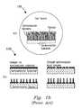
- FIG. 1 bcontains illustrations depicting VLS and SLS applied to monolithic substrates.
- VLS growth 101the semiconductor material is supplied as a gas and is adsorbed by liquid nanodroplets of an appropriate catalytic material formed on a substrate. The nanodroplets serve as seeds for nanowire growth. The semiconductor material condenses at the interface between the droplet and the nanowire.
- the SLS process 102is similar to VLS growth except that in SLS growth, the semiconductor material is supplied as a solid.
- the catalyst and the semiconductor materialform a liquid mixture from which the semiconductor material condenses to form the semiconductor nanowire.
- the semiconductor materialcan comprise a powder, rather than a monolithic substrate, and the powder granules are coated with the catalyst.
- the use of the semiconductor powdercan lead to three dimensional growth 104 that is easily scalable.
- the present inventionincludes methods of fabricating nanowires comprising first and second elements.
- the methodscan be characterized by coating solid powder granules, which comprise a first element, with a catalyst.
- the catalyst and the first elementshould form liquid when heated, mixed phase having a eutectic or peritectic point.
- the granules, which have been coated with the catalystcan then be heated to a temperature greater than or equal to the eutectic or peritectic point.
- a vapor sourcecomprising the second element is introduced.
- the vapor sourcechemically interacts with the liquid, mixed phase to consume the first element and to induce condensation of a product that comprises the first and second elements in the form of a nanowire.
- the methods of the present inventionrequire the presence of both a vapor source and a solid source, and can be used to synthesize nanowires comprising multiple elements.
- the producthas a higher melting point than that of the first element.
- the first elementcomprises silicon.
- the second elementcan then comprise oxygen, nitrogen, carbon, or silicon.
- the resultant nanowireswould then comprise silicon oxide, silicon nitride, silicon carbide, or substantially pure silicon respectively.
- silicon-containing nanowires synthesized according to embodiments of the present inventioncan be formed into an electrode in an energy storage device having a discharge capacity greater than or equal to 400 mAh/g. In another embodiment, the discharge capacity is greater than or equal to 1300 mAh/g.
- An exemplary energy storage deviceincludes, but is not limited to a Li-ion battery.
- Synthesis of nanowires comprising predominantly siliconcan be accomplished according to embodiments of the present invention when both the solid source and the vapor source comprise silicon.
- a specific exampleinvolves using SiCl 4 as the vapor source.
- a suitable catalystcan comprise nickel.
- the nickel-coated silicon powdercan be heated to a temperature between 900° C. and 1050° C.
- the first elementcan comprise other semiconducting elements or elements that form semiconducting materials when combined with the second element.
- the first elementcan comprise Ge or Sn.
- the second elementcan then comprise oxygen, nitrogen, carbon, or combinations thereof.
- Suitable catalystscan include, but are not limited to, Ni, Fe, Al, Au, and Cu or combinations thereof.
- FIG. 1 a and 1 bare illustrations depicting 2-D and 3-D growth using SLS and/or VLS processes.
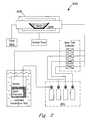
- FIG. 2is a diagram of an exemplary apparatus for synthesizing nanowires according to embodiments of the present invention.
- FIG. 3is a block diagram depicting methods of synthesizing nanowires according to embodiments of the present invention.
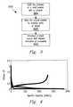
- FIG. 4is a plot showing the charge/discharge profile and specific capacity of Si-based nanowires formed into electrodes for Li-ion batteries according to embodiments of the present invention.
- one or more elements from a vapor sourceare used to induce nanowire growth from a solid source. Accordingly, the vapor-induced solid-liquid-solid (VI-SLS) approach requires the presence of both vapor and solid sources.
- FIGS. 2 and 3show various aspects and/or embodiments of the present invention.
- the illustrationdepicts an exemplary apparatus 200 for nanowire growth.
- One or more gases 201which comprise an element that induces nanowire growth or that serves as a cover gas, can be introduced into the furnace 206 through the vapor lines 202 .
- the solid powder 203 coated with a catalystcan be contained in the furnace in the ceramic holder 205 , while a pump 204 evacuates gases from the furnace.
- a block diagram 300depicts the methods of the present invention.
- the methodscomprise coating 301 solid powder granules, which comprise a first element, with a catalyst.
- the catalyst and the first elementshould form when heated a liquid, mixed phase having a eutectic or peritectic point.
- the granules, which have been coated with the catalystcan then be heated 302 to a temperature greater than or equal to the eutectic or peritectic point.
- a vapor sourcecomprising the second element is introduced 303 .
- the vapor sourcechemically interacts with the liquid, mixed phase to consume the first element and to induce condensation of a product that comprises the first and second elements in the form of a nanowire.
- the methods of the present inventionrequire the presence of both a vapor source and a solid source, and can be used to synthesize nanowires comprising multiple elements.
- Si nanowirescan be prepared from Si powder and a carbon-containing gas.
- the growthshould occur in a carbon-free furnace, such as a quartz tube furnace.
- the silicon powderis the solid source and is coated with a nickel catalyst.
- An exemplary carbon-containing gasincludes CH 4 .
- the nickel-coated Si powderis prepared by grinding as-received, fine Si powder and then coating with Ni using a 10% solution of Ni(NO 3 ) 2 .6H 2 O in water. The Ni-coated Si powder can then be dried and placed in a ceramic boat in the center of the furnace.
- the furnaceis pumped to reduced pressure (e.g., 10 ⁇ 3 Torr) and refilled with an Ar/H 2 gas mixture (2.75% H 2 ). This process is repeated three times to minimize the residual air and contamination in the tube furnace.
- the furnacecan be filled with an Ar/H 2 gas mixture (2.75% H 2 ) and approximately 1% CH 4 gas.
- the furnace pressureis controlled at approximately 15 Torr by adjusting the gas flow rate and the pumping speed.
- the furnaceis heated a rate of 5° C./min to 500° C. and held at this temperature for 1 h.
- the temperature in the furnaceis then increased at a rate of 10° C./min to 950° C. and held at this temperature for 2 to 6 hours.
- the furnaceis allowed to cool to room temperature in a rate of 10° C./min.
- the reaction processcan be expressed as follows.
- the aspects of the present inventioncan be applied to synthesize silicon nitride nanowires.
- the vapor sourcewould comprise a nitrogen-containing gas such as NH 3 .
- the appropriate reaction processcan be expressed as follows.
- substantially pure silicon nanowirescan be prepared by introducing a vapor source comprising Si.
- the Si from the vapor sourcecan react with the Si in the liquid, mixed phase to produce silicon nanowires.
- An exemplary vapor sourcecan include, but is not limited to, SiCl 4 . Since SiCl 4 is a liquid at room temperature, it can be introduced into the furnace by a bubbler system using an inert carrier gas and/or by a liquid delivery system and vaporizer apparatus. The reaction process can be expressed as follows.
- SiO x nanowires with substantially no SiC corecan be prepared in a quartz tube furnace with minimal carbon contaminants.
- fine Si powderis ground for use as a solid silicon source.
- the ground samplewas then coated with 10% Ni using Ni(NO 3 )2.6 H 2 O in water solution.
- the dried powderwas placed in a ceramic boat and placed in the center of the furnace.
- the furnacewas pumped down to 10 ⁇ 3 Torr and refilled with Ar/H 2 mixture (2.75% H2).
- Oxygen gaswas used as the second element.
- the furnacewas heated at a rate of 5° C./min to 500° C. and held at this temperature for 1 h, then heated at a rate of 10° C./min to 950° C. and held at this temperature for 2 to 6 hours.
- the samplewas cooled to room temperature in a rate of 10° C./min.
- This reaction processcan be expressed as follows.
- a plotshows the charge/discharge profile and specific capacity of SiO 1.8 nanowires formed into an electrode in a Li-ion battery.
- the sample testedresulted in an initial charge capacity of 1800 mAh/g and a discharge capacity of 1300 mAh/g.
- the batterywas prepared as follows.
- the Si-based nanowires(80% weight) were mixed with 10 wt. % of super P carbon and 10 wt. % PVDF binder.
- NMPN-Methyl-2-pyrrolidone
- the slurrywas then cast on a Cu foil. The thickness of the cathode is ⁇ 0.2 mm thick.
- Electrochemical performance of the Si based anodewas tested in a coin cell (type 2325) configuration. Li metal and a porous membrane was used as the counter electrode and separator, respectively. 1M LiPF 6 in EC:DEC (1:1) was used as an electrolyte. The coin cell was assembled in an argon filled glove box. Batteries were tested in a Battery Testing System to produce the plot in FIG. 4 .
- the prevailing mechanism for nanowire growthappears to be the reaction between elements in the vapor source and the semiconductor constituent in the liquid, mixed phase comprising the semiconductor and the catalyst.
- the consumption of the semiconductor element from the liquid mixed phaseestablishes a gradient that draws additional semiconductor material from the solid source. Accordingly, the semiconductor powder granules are consumed during nanowire synthesis.
- Suitable materialscan include, but are not limited to, Ge and Sn.
- vapor sources that contain oxygen, carbon, or nitrogennanowires comprising Ge, Ge 3 N 4 , GeO, GeO 2 , Sn, SnO, SnO 2 , etc., can be produced.
- Suitable catalysts for these growthscan include, but are not limited to Ni, Fe, Al, Au, Cu, etc. The temperature for these growths will vary depending on the material system, but should generally occur at, or above, the approximate eutectic or peritectic point.
Landscapes
- Chemical & Material Sciences (AREA)
- Engineering & Computer Science (AREA)
- Nanotechnology (AREA)
- Organic Chemistry (AREA)
- Chemical Kinetics & Catalysis (AREA)
- Inorganic Chemistry (AREA)
- Electrochemistry (AREA)
- General Chemical & Material Sciences (AREA)
- General Physics & Mathematics (AREA)
- Materials Engineering (AREA)
- Crystallography & Structural Chemistry (AREA)
- Condensed Matter Physics & Semiconductors (AREA)
- Physics & Mathematics (AREA)
- Composite Materials (AREA)
- Manufacturing & Machinery (AREA)
- Battery Electrode And Active Subsutance (AREA)
Abstract
Description


Claims (11)
Priority Applications (3)
| Application Number | Priority Date | Filing Date | Title |
|---|---|---|---|
| US12/368,711US8110167B2 (en) | 2009-02-10 | 2009-02-10 | Nanowire synthesis from vapor and solid sources |
| PCT/US2010/021450WO2010093500A1 (en) | 2009-02-10 | 2010-01-20 | Nanowire synthesis from vapor and solid sources and energy storage device |
| US13/339,214US20120107213A1 (en) | 2009-02-10 | 2011-12-28 | Energy Storage Devices Having Electrodes Comprising Nanowires |
Applications Claiming Priority (1)
| Application Number | Priority Date | Filing Date | Title |
|---|---|---|---|
| US12/368,711US8110167B2 (en) | 2009-02-10 | 2009-02-10 | Nanowire synthesis from vapor and solid sources |
Related Child Applications (1)
| Application Number | Title | Priority Date | Filing Date |
|---|---|---|---|
| US13/339,214DivisionUS20120107213A1 (en) | 2009-02-10 | 2011-12-28 | Energy Storage Devices Having Electrodes Comprising Nanowires |
Publications (2)
| Publication Number | Publication Date |
|---|---|
| US20100202952A1 US20100202952A1 (en) | 2010-08-12 |
| US8110167B2true US8110167B2 (en) | 2012-02-07 |
Family
ID=42016955
Family Applications (2)
| Application Number | Title | Priority Date | Filing Date |
|---|---|---|---|
| US12/368,711Expired - Fee RelatedUS8110167B2 (en) | 2009-02-10 | 2009-02-10 | Nanowire synthesis from vapor and solid sources |
| US13/339,214AbandonedUS20120107213A1 (en) | 2009-02-10 | 2011-12-28 | Energy Storage Devices Having Electrodes Comprising Nanowires |
Family Applications After (1)
| Application Number | Title | Priority Date | Filing Date |
|---|---|---|---|
| US13/339,214AbandonedUS20120107213A1 (en) | 2009-02-10 | 2011-12-28 | Energy Storage Devices Having Electrodes Comprising Nanowires |
Country Status (2)
| Country | Link |
|---|---|
| US (2) | US8110167B2 (en) |
| WO (1) | WO2010093500A1 (en) |
Families Citing this family (3)
| Publication number | Priority date | Publication date | Assignee | Title |
|---|---|---|---|---|
| US8610100B2 (en)* | 2009-06-30 | 2013-12-17 | Nokia Corporation | Apparatus comprising nanowires |
| KR101575438B1 (en) | 2013-12-27 | 2015-12-07 | 현대자동차주식회사 | Silicon nanowires embedded in nickel silicide nanowires for lithium-based battery anodes |
| FR3069461B1 (en) | 2017-07-28 | 2021-12-24 | Enwires | NANOSTRUCTURED MATERIAL AND METHOD FOR PREPARING IT |
Citations (8)
| Publication number | Priority date | Publication date | Assignee | Title |
|---|---|---|---|---|
| WO2005119753A2 (en) | 2004-04-30 | 2005-12-15 | Nanosys, Inc. | Systems and methods for nanowire growth and harvesting |
| US20060046480A1 (en)* | 2003-10-16 | 2006-03-02 | Ting Guo | Nanostructures, nanogrooves, and nanowires |
| US20070105356A1 (en)* | 2005-11-10 | 2007-05-10 | Wei Wu | Method of controlling nanowire growth and device with controlled-growth nanowire |
| US7297446B2 (en) | 2003-03-28 | 2007-11-20 | Sanyo Electric Co., Ltd. | Negative electrode for rechargeable lithium battery and method for fabrication thereof |
| US7335259B2 (en) | 2003-07-08 | 2008-02-26 | Brian A. Korgel | Growth of single crystal nanowires |
| US20080261112A1 (en)* | 2007-04-17 | 2008-10-23 | Kaoru Nagata | Electrode material for electrochemcial device, method for producing the same, electrode using the electrode material, and electrochemical device using the electrode material |
| US20090042102A1 (en) | 2007-08-10 | 2009-02-12 | Yi Cui | Nanowire Battery Methods and Arrangements |
| US20090176159A1 (en) | 2008-01-09 | 2009-07-09 | Aruna Zhamu | Mixed nano-filament electrode materials for lithium ion batteries |
Family Cites Families (2)
| Publication number | Priority date | Publication date | Assignee | Title |
|---|---|---|---|---|
| TWI387150B (en)* | 2007-09-06 | 2013-02-21 | Canon Kk | Release material manufacturing method, lithium ion accumulation. A release material, and an electrode structure and a power storage device using the same |
| US8936874B2 (en)* | 2008-06-04 | 2015-01-20 | Nanotek Instruments, Inc. | Conductive nanocomposite-based electrodes for lithium batteries |
- 2009
- 2009-02-10USUS12/368,711patent/US8110167B2/ennot_activeExpired - Fee Related
- 2010
- 2010-01-20WOPCT/US2010/021450patent/WO2010093500A1/enactiveApplication Filing
- 2011
- 2011-12-28USUS13/339,214patent/US20120107213A1/ennot_activeAbandoned
Patent Citations (8)
| Publication number | Priority date | Publication date | Assignee | Title |
|---|---|---|---|---|
| US7297446B2 (en) | 2003-03-28 | 2007-11-20 | Sanyo Electric Co., Ltd. | Negative electrode for rechargeable lithium battery and method for fabrication thereof |
| US7335259B2 (en) | 2003-07-08 | 2008-02-26 | Brian A. Korgel | Growth of single crystal nanowires |
| US20060046480A1 (en)* | 2003-10-16 | 2006-03-02 | Ting Guo | Nanostructures, nanogrooves, and nanowires |
| WO2005119753A2 (en) | 2004-04-30 | 2005-12-15 | Nanosys, Inc. | Systems and methods for nanowire growth and harvesting |
| US20070105356A1 (en)* | 2005-11-10 | 2007-05-10 | Wei Wu | Method of controlling nanowire growth and device with controlled-growth nanowire |
| US20080261112A1 (en)* | 2007-04-17 | 2008-10-23 | Kaoru Nagata | Electrode material for electrochemcial device, method for producing the same, electrode using the electrode material, and electrochemical device using the electrode material |
| US20090042102A1 (en) | 2007-08-10 | 2009-02-12 | Yi Cui | Nanowire Battery Methods and Arrangements |
| US20090176159A1 (en) | 2008-01-09 | 2009-07-09 | Aruna Zhamu | Mixed nano-filament electrode materials for lithium ion batteries |
Non-Patent Citations (9)
| Title |
|---|
| Chan, Candace K., et al., "High-performance lithium battery anodes using silicon nanowires", Nature Nanotechnology, Jan. 2008, 31-35 pps., vol. 3, Stanford, CA, USA. |
| Chang, J.B., et al.; "Ultrafast growth of single-crystalline Si nanowired", Materials Letters, 2006, 2125-2128 pps., vol. 60, Elsevier. |
| Kim, Hyunjung, "Three-Dimensional Porous Silicon Particles for Use in High-Performance Lithium Secondary Batteries," Angew. Chem. Int. Ed, 2008, vol. 47, pp. 1-5, Wiley-VCH Verlag InterScience, Hanyang University, Ansan, Korea. |
| Lee, Kun-Hong, Ph.D., "Synthesis of Si nanowires for an anode material of Li batteries", Defense Technical Information Center Report; Jun. 28, 2006-Nov. 1, 2007, 30 pages, South Korea. |
| PCT International Search Report and Written Opinion. |
| Sunkara, M.K., et al., "Bulk synthesis of silcon nanowires using a low-temperature vapor-liquid-solid method", Applied Physics Letters, Sep. 3, 2001, 1546-1548 pps., vol. 79, No. 10, Louisville, KY, USA. |
| Xing, Y.J., et al., "Silicon nanowires grown from Au-coated Si substrate", Applied Physics A, 2002, 551-553 pps., vol. 76, Springer-Verlag, China. |
| Yan, H.F., et al., "Growth of amorphous silicon nanowires via a solid-liquid-mechanism", Chemical Physics Letters, Jun. 16, 2000, 224-228 pps., vol. 323, Elsevier, China. |
| Yu, D.P., et al., "Controlled growth of oriented amorphous silicon nanowires via a solid-liquid-solid (SLS) mechanism", Physica E, 2001, 305-309 pps., Elsevier, China. |
Also Published As
| Publication number | Publication date |
|---|---|
| WO2010093500A1 (en) | 2010-08-19 |
| US20100202952A1 (en) | 2010-08-12 |
| US20120107213A1 (en) | 2012-05-03 |
Similar Documents
| Publication | Publication Date | Title |
|---|---|---|
| CN108511794B (en) | Oxide all-solid-state battery | |
| US20170162868A1 (en) | Conductive single crystal silicon particles coated with highly conductive carbon containing nanopores and ultrathin metal film, high capacity lithium anode material including the same, and preparing method thereof | |
| Güneş | A direct synthesis of Si-nanowires on 3D porous graphene as a high performance anode material for Li-ion batteries | |
| EP3464176B1 (en) | Method for producing a silicon nitride powder and battery comprising the powder | |
| CN104103821B (en) | The preparation method of silicon-carbon cathode material | |
| Hao et al. | Ionic liquid electrodeposition of strain-released Germanium nanowires as stable anodes for lithium ion batteries | |
| US8591990B2 (en) | Microfiber supported metal silicide nanowires | |
| Lu et al. | Facile synthesis of carbon decorated silicon nanotube arrays as anode material for high-performance lithium-ion batteries | |
| JP2024536764A (en) | New composite material for lithium secondary batteries and its preparation method and application | |
| US8110167B2 (en) | Nanowire synthesis from vapor and solid sources | |
| CN105814716B (en) | Positive electrode for lithium-sulfur secondary battery and method for forming same | |
| KR101487079B1 (en) | Electrode for lithium secondary battery, lithium secondary battery using the same and fabrication method thereof | |
| KR101418835B1 (en) | Manufacturing method for cathode materials for secondary cell | |
| CN105714370A (en) | Method for preparing tin whiskers in large scale | |
| CN114142016B (en) | Micron-sized lamellar Si/SiO2Composite material, preparation method and application thereof | |
| KR102670074B1 (en) | Apparatus and method for manufacturing hexagonal Si crystal | |
| KR101298128B1 (en) | Fabrication method of Li-ion battery anode using Sn-SnO hybrid nanostructures | |
| US20220246932A1 (en) | Electrode, electrical energy storage device & method | |
| Lee et al. | One-minute deposition of micrometre-thick porous Si anodes for lithium ion batteries | |
| US20230077180A1 (en) | Electrode, energy storage device and method | |
| CN120117591B (en) | Preparation method of multi-order ordered silicon-carbon anode material | |
| US20240128439A1 (en) | Cyclohexasilane for electrodes | |
| KR101872920B1 (en) | Method of anode material for lithium ion battery using transition metal chalcogen compounds, and anode material for lithium ion battery and lithium ion battery using this | |
| Bogart | Silicon nanowires: synthesis and use as lithium-ion battery anodes | |
| CN104752701A (en) | Silicon Nanowire Structure Embedded In Nickel Silicide Nanowires For Lithium-based Battery Anodes |
Legal Events
| Date | Code | Title | Description |
|---|---|---|---|
| AS | Assignment | Owner name:BATTELLE MEMORIAL INSTITUTE, WASHINGTON Free format text:ASSIGNMENT OF ASSIGNORS INTEREST;ASSIGNORS:ZHANG, JIGUANG;LIU, JUN;YANG, ZHENGUO;AND OTHERS;REEL/FRAME:022236/0136 Effective date:20090205 | |
| ZAAA | Notice of allowance and fees due | Free format text:ORIGINAL CODE: NOA | |
| ZAAB | Notice of allowance mailed | Free format text:ORIGINAL CODE: MN/=. | |
| AS | Assignment | Owner name:BATTELLE MEMORIAL INSTITUTE, WASHINGTON Free format text:ASSIGNMENT OF ASSIGNORS INTEREST;ASSIGNORS:ZHANG, JIGUANG;LIU, JUN;YANG, ZHENGUO;AND OTHERS;REEL/FRAME:027454/0690 Effective date:20090205 | |
| STCF | Information on status: patent grant | Free format text:PATENTED CASE | |
| FPAY | Fee payment | Year of fee payment:4 | |
| MAFP | Maintenance fee payment | Free format text:PAYMENT OF MAINTENANCE FEE, 8TH YR, SMALL ENTITY (ORIGINAL EVENT CODE: M2552); ENTITY STATUS OF PATENT OWNER: SMALL ENTITY Year of fee payment:8 | |
| FEPP | Fee payment procedure | Free format text:MAINTENANCE FEE REMINDER MAILED (ORIGINAL EVENT CODE: REM.); ENTITY STATUS OF PATENT OWNER: SMALL ENTITY | |
| LAPS | Lapse for failure to pay maintenance fees | Free format text:PATENT EXPIRED FOR FAILURE TO PAY MAINTENANCE FEES (ORIGINAL EVENT CODE: EXP.); ENTITY STATUS OF PATENT OWNER: SMALL ENTITY | |
| STCH | Information on status: patent discontinuation | Free format text:PATENT EXPIRED DUE TO NONPAYMENT OF MAINTENANCE FEES UNDER 37 CFR 1.362 | |
| FP | Lapsed due to failure to pay maintenance fee | Effective date:20240207 |