US8101261B2 - One-dimensional arrays of block copolymer cylinders and applications thereof - Google Patents
One-dimensional arrays of block copolymer cylinders and applications thereofDownload PDFInfo
- Publication number
- US8101261B2 US8101261B2US12/030,562US3056208AUS8101261B2US 8101261 B2US8101261 B2US 8101261B2US 3056208 AUS3056208 AUS 3056208AUS 8101261 B2US8101261 B2US 8101261B2
- Authority
- US
- United States
- Prior art keywords
- block copolymer
- trench
- block
- polymer
- substrate
- Prior art date
- Legal status (The legal status is an assumption and is not a legal conclusion. Google has not performed a legal analysis and makes no representation as to the accuracy of the status listed.)
- Active, expires
Links
- 229920001400block copolymerPolymers0.000titleclaimsabstractdescription196
- 238000003491arrayMethods0.000titleabstractdescription4
- 238000000034methodMethods0.000claimsabstractdescription72
- 239000000463materialSubstances0.000claimsdescription225
- 239000000758substrateSubstances0.000claimsdescription117
- 229920000642polymerPolymers0.000claimsdescription113
- 238000009736wettingMethods0.000claimsdescription93
- 239000004793PolystyreneSubstances0.000claimsdescription52
- 239000011159matrix materialSubstances0.000claimsdescription51
- 230000007935neutral effectEffects0.000claimsdescription49
- 229920002223polystyrenePolymers0.000claimsdescription47
- 238000000137annealingMethods0.000claimsdescription33
- 229920003171Poly (ethylene oxide)Polymers0.000claimsdescription30
- 239000000203mixtureSubstances0.000claimsdescription30
- 229920000747poly(lactic acid)Polymers0.000claimsdescription24
- 239000002904solventSubstances0.000claimsdescription24
- 239000002861polymer materialSubstances0.000claimsdescription23
- 239000004926polymethyl methacrylateSubstances0.000claimsdescription22
- 229910052710siliconInorganic materials0.000claimsdescription22
- XUIMIQQOPSSXEZ-UHFFFAOYSA-NSiliconChemical compound[Si]XUIMIQQOPSSXEZ-UHFFFAOYSA-N0.000claimsdescription21
- 229920005604random copolymerPolymers0.000claimsdescription21
- 239000010703siliconSubstances0.000claimsdescription21
- 229920003229poly(methyl methacrylate)Polymers0.000claimsdescription20
- 229920001519homopolymerPolymers0.000claimsdescription14
- VYPSYNLAJGMNEJ-UHFFFAOYSA-NSilicium dioxideChemical compoundO=[Si]=OVYPSYNLAJGMNEJ-UHFFFAOYSA-N0.000claimsdescription12
- 238000005530etchingMethods0.000claimsdescription12
- 229910052814silicon oxideInorganic materials0.000claimsdescription8
- 229910052751metalInorganic materials0.000claimsdescription6
- 239000002184metalSubstances0.000claimsdescription6
- 229910052581Si3N4Inorganic materials0.000claimsdescription5
- 238000004132cross linkingMethods0.000claimsdescription5
- HQVNEWCFYHHQES-UHFFFAOYSA-Nsilicon nitrideChemical compoundN12[Si]34N5[Si]62N3[Si]51N64HQVNEWCFYHHQES-UHFFFAOYSA-N0.000claimsdescription5
- CERQOIWHTDAKMF-UHFFFAOYSA-MMethacrylateChemical compoundCC(=C)C([O-])=OCERQOIWHTDAKMF-UHFFFAOYSA-M0.000claimsdescription4
- 238000011049fillingMethods0.000claimsdescription4
- AMGQUBHHOARCQH-UHFFFAOYSA-Nindium;oxotinChemical compound[In].[Sn]=OAMGQUBHHOARCQH-UHFFFAOYSA-N0.000claimsdescription4
- 238000000926separation methodMethods0.000claimsdescription3
- 229910001092metal group alloyInorganic materials0.000claimsdescription2
- KNCYXPMJDCCGSJ-UHFFFAOYSA-Npiperidine-2,6-dioneChemical compoundO=C1CCCC(=O)N1KNCYXPMJDCCGSJ-UHFFFAOYSA-N0.000claimsdescription2
- 229920006395saturated elastomerPolymers0.000claimsdescription2
- 238000000151depositionMethods0.000claims5
- 229920000361Poly(styrene)-block-poly(ethylene glycol)Polymers0.000claims1
- 239000012212insulatorSubstances0.000claims1
- 229920005553polystyrene-acrylatePolymers0.000claims1
- KONHVWVBPIDGBH-UHFFFAOYSA-Ntrichloro-[3-(4-methoxyphenyl)propyl]silaneChemical compoundCOC1=CC=C(CCC[Si](Cl)(Cl)Cl)C=C1KONHVWVBPIDGBH-UHFFFAOYSA-N0.000claims1
- 239000010410layerSubstances0.000description47
- 229920001577copolymerPolymers0.000description35
- 239000004626polylactic acidSubstances0.000description18
- 239000010408filmSubstances0.000description17
- 229920000359diblock copolymerPolymers0.000description16
- -1poly(acrylate)Polymers0.000description10
- 125000006850spacer groupChemical group0.000description10
- YXFVVABEGXRONW-UHFFFAOYSA-NTolueneChemical compoundCC1=CC=CC=C1YXFVVABEGXRONW-UHFFFAOYSA-N0.000description9
- 230000015572biosynthetic processEffects0.000description8
- 238000000206photolithographyMethods0.000description7
- 239000004065semiconductorSubstances0.000description7
- QTBSBXVTEAMEQO-UHFFFAOYSA-NAcetic acidChemical compoundCC(O)=OQTBSBXVTEAMEQO-UHFFFAOYSA-N0.000description6
- UHOVQNZJYSORNB-UHFFFAOYSA-NBenzeneChemical compoundC1=CC=CC=C1UHOVQNZJYSORNB-UHFFFAOYSA-N0.000description6
- PPBRXRYQALVLMV-UHFFFAOYSA-NStyreneChemical compoundC=CC1=CC=CC=C1PPBRXRYQALVLMV-UHFFFAOYSA-N0.000description6
- 238000001020plasma etchingMethods0.000description6
- 238000004528spin coatingMethods0.000description6
- 235000012431wafersNutrition0.000description6
- 239000000470constituentSubstances0.000description5
- 230000000737periodic effectEffects0.000description5
- 239000010409thin filmSubstances0.000description5
- 229920000428triblock copolymerPolymers0.000description5
- HEDRZPFGACZZDS-UHFFFAOYSA-NChloroformChemical compoundClC(Cl)ClHEDRZPFGACZZDS-UHFFFAOYSA-N0.000description4
- 229920000390Poly(styrene-block-methyl methacrylate)Polymers0.000description4
- 239000012634fragmentSubstances0.000description4
- 238000004519manufacturing processMethods0.000description4
- 238000000059patterningMethods0.000description4
- 238000001338self-assemblyMethods0.000description4
- XLYOFNOQVPJJNP-UHFFFAOYSA-NwaterSubstancesOXLYOFNOQVPJJNP-UHFFFAOYSA-N0.000description4
- KRHYYFGTRYWZRS-UHFFFAOYSA-NFluoraneChemical compoundFKRHYYFGTRYWZRS-UHFFFAOYSA-N0.000description3
- OKKJLVBELUTLKV-UHFFFAOYSA-NMethanolChemical compoundOCOKKJLVBELUTLKV-UHFFFAOYSA-N0.000description3
- HEMHJVSKTPXQMS-UHFFFAOYSA-MSodium hydroxideChemical compound[OH-].[Na+]HEMHJVSKTPXQMS-UHFFFAOYSA-M0.000description3
- 230000009477glass transitionEffects0.000description3
- 238000010438heat treatmentMethods0.000description3
- 229920006030multiblock copolymerPolymers0.000description3
- 229920002120photoresistant polymerPolymers0.000description3
- 229940065514poly(lactide)Drugs0.000description3
- 229920000193polymethacrylatePolymers0.000description3
- 239000002094self assembled monolayerSubstances0.000description3
- 239000013545self-assembled monolayerSubstances0.000description3
- 239000002356single layerSubstances0.000description3
- MYRTYDVEIRVNKP-UHFFFAOYSA-N1,2-DivinylbenzeneChemical compoundC=CC1=CC=CC=C1C=CMYRTYDVEIRVNKP-UHFFFAOYSA-N0.000description2
- UFHFLCQGNIYNRP-UHFFFAOYSA-NHydrogenChemical compound[H][H]UFHFLCQGNIYNRP-UHFFFAOYSA-N0.000description2
- WOBHKFSMXKNTIM-UHFFFAOYSA-NHydroxyethyl methacrylateChemical compoundCC(=C)C(=O)OCCOWOBHKFSMXKNTIM-UHFFFAOYSA-N0.000description2
- VVQNEPGJFQJSBK-UHFFFAOYSA-NMethyl methacrylateChemical compoundCOC(=O)C(C)=CVVQNEPGJFQJSBK-UHFFFAOYSA-N0.000description2
- DTQVDTLACAAQTR-UHFFFAOYSA-NTrifluoroacetic acidChemical compoundOC(=O)C(F)(F)FDTQVDTLACAAQTR-UHFFFAOYSA-N0.000description2
- MCMNRKCIXSYSNV-UHFFFAOYSA-NZirconium dioxideChemical compoundO=[Zr]=OMCMNRKCIXSYSNV-UHFFFAOYSA-N0.000description2
- 238000000429assemblyMethods0.000description2
- 230000000712assemblyEffects0.000description2
- 238000004630atomic force microscopyMethods0.000description2
- QVGXLLKOCUKJST-UHFFFAOYSA-Natomic oxygenChemical compound[O]QVGXLLKOCUKJST-UHFFFAOYSA-N0.000description2
- AIYUHDOJVYHVIT-UHFFFAOYSA-Mcaesium chlorideChemical compound[Cl-].[Cs+]AIYUHDOJVYHVIT-UHFFFAOYSA-M0.000description2
- 239000003990capacitorSubstances0.000description2
- 238000005266castingMethods0.000description2
- 229910052681coesiteInorganic materials0.000description2
- 229910052906cristobaliteInorganic materials0.000description2
- 229920006037cross link polymerPolymers0.000description2
- 230000003247decreasing effectEffects0.000description2
- 239000001257hydrogenSubstances0.000description2
- 229910052739hydrogenInorganic materials0.000description2
- 229910000040hydrogen fluorideInorganic materials0.000description2
- 125000002887hydroxy groupChemical group[H]O*0.000description2
- 125000005647linker groupChemical group0.000description2
- KWGKDLIKAYFUFQ-UHFFFAOYSA-Mlithium chlorideChemical compound[Li+].[Cl-]KWGKDLIKAYFUFQ-UHFFFAOYSA-M0.000description2
- 238000001459lithographyMethods0.000description2
- 229920002521macromoleculePolymers0.000description2
- 239000000178monomerSubstances0.000description2
- 239000001301oxygenSubstances0.000description2
- 229910052760oxygenInorganic materials0.000description2
- 238000009832plasma treatmentMethods0.000description2
- 229920000058polyacrylatePolymers0.000description2
- 230000005855radiationEffects0.000description2
- 239000000377silicon dioxideSubstances0.000description2
- 239000000243solutionSubstances0.000description2
- 229910052682stishoviteInorganic materials0.000description2
- 239000000126substanceSubstances0.000description2
- 229910052905tridymiteInorganic materials0.000description2
- 229920002818(Hydroxyethyl)methacrylatePolymers0.000description1
- SCYULBFZEHDVBN-UHFFFAOYSA-N1,1-DichloroethaneChemical compoundCC(Cl)ClSCYULBFZEHDVBN-UHFFFAOYSA-N0.000description1
- DDFHBQSCUXNBSA-UHFFFAOYSA-N5-(5-carboxythiophen-2-yl)thiophene-2-carboxylic acidChemical compoundS1C(C(=O)O)=CC=C1C1=CC=C(C(O)=O)S1DDFHBQSCUXNBSA-UHFFFAOYSA-N0.000description1
- KRHYYFGTRYWZRS-UHFFFAOYSA-MFluoride anionChemical compound[F-]KRHYYFGTRYWZRS-UHFFFAOYSA-M0.000description1
- YZCKVEUIGOORGS-UHFFFAOYSA-NHydrogen atomChemical compound[H]YZCKVEUIGOORGS-UHFFFAOYSA-N0.000description1
- 208000034530PLAA-associated neurodevelopmental diseaseDiseases0.000description1
- 229910002370SrTiO3Inorganic materials0.000description1
- XXFXTBNFFMQVKJ-UHFFFAOYSA-N[diphenyl(trityloxy)methyl]benzeneChemical compoundC=1C=CC=CC=1C(C=1C=CC=CC=1)(C=1C=CC=CC=1)OC(C=1C=CC=CC=1)(C=1C=CC=CC=1)C1=CC=CC=C1XXFXTBNFFMQVKJ-UHFFFAOYSA-N0.000description1
- 239000002253acidSubstances0.000description1
- 230000006978adaptationEffects0.000description1
- 229920003232aliphatic polyesterPolymers0.000description1
- 229910052782aluminiumInorganic materials0.000description1
- PNEYBMLMFCGWSK-UHFFFAOYSA-Naluminium oxideInorganic materials[O-2].[O-2].[O-2].[Al+3].[Al+3]PNEYBMLMFCGWSK-UHFFFAOYSA-N0.000description1
- LDDQLRUQCUTJBB-UHFFFAOYSA-Nammonium fluorideChemical compound[NH4+].[F-]LDDQLRUQCUTJBB-UHFFFAOYSA-N0.000description1
- 239000011260aqueous acidSubstances0.000description1
- 239000007864aqueous solutionSubstances0.000description1
- 238000010504bond cleavage reactionMethods0.000description1
- XQPRBTXUXXVTKB-UHFFFAOYSA-Mcaesium iodideInorganic materials[I-].[Cs+]XQPRBTXUXXVTKB-UHFFFAOYSA-M0.000description1
- 238000009833condensationMethods0.000description1
- 230000005494condensationEffects0.000description1
- 238000010276constructionMethods0.000description1
- 238000001816coolingMethods0.000description1
- 229910052802copperInorganic materials0.000description1
- 229910052593corundumInorganic materials0.000description1
- 239000003431cross linking reagentSubstances0.000description1
- 238000010894electron beam technologyMethods0.000description1
- 238000000609electron-beam lithographyMethods0.000description1
- 238000000572ellipsometryMethods0.000description1
- 238000001704evaporationMethods0.000description1
- 230000008020evaporationEffects0.000description1
- 238000001900extreme ultraviolet lithographyMethods0.000description1
- 238000009472formulationMethods0.000description1
- PCHJSUWPFVWCPO-UHFFFAOYSA-NgoldChemical compound[Au]PCHJSUWPFVWCPO-UHFFFAOYSA-N0.000description1
- 239000010931goldSubstances0.000description1
- 229910052737goldInorganic materials0.000description1
- 229920000578graft copolymerPolymers0.000description1
- CJNBYAVZURUTKZ-UHFFFAOYSA-Nhafnium(IV) oxideInorganic materialsO=[Hf]=OCJNBYAVZURUTKZ-UHFFFAOYSA-N0.000description1
- XMBWDFGMSWQBCA-UHFFFAOYSA-Nhydrogen iodideChemical compoundIXMBWDFGMSWQBCA-UHFFFAOYSA-N0.000description1
- 229940071870hydroiodic acidDrugs0.000description1
- 238000011065in-situ storageMethods0.000description1
- 239000011810insulating materialSubstances0.000description1
- HSZCZNFXUDYRKD-UHFFFAOYSA-Mlithium iodideInorganic materials[Li+].[I-]HSZCZNFXUDYRKD-UHFFFAOYSA-M0.000description1
- 239000002086nanomaterialSubstances0.000description1
- 239000002105nanoparticleSubstances0.000description1
- TVMXDCGIABBOFY-UHFFFAOYSA-NoctaneChemical compoundCCCCCCCCTVMXDCGIABBOFY-UHFFFAOYSA-N0.000description1
- 230000003287optical effectEffects0.000description1
- 239000003960organic solventSubstances0.000description1
- RUVINXPYWBROJD-UHFFFAOYSA-Npara-methoxyphenylNatural productsCOC1=CC=C(C=CC)C=C1RUVINXPYWBROJD-UHFFFAOYSA-N0.000description1
- 229920006254polymer filmPolymers0.000description1
- 238000003672processing methodMethods0.000description1
- 238000010526radical polymerization reactionMethods0.000description1
- 150000003839saltsChemical class0.000description1
- 238000004626scanning electron microscopyMethods0.000description1
- 230000007017scissionEffects0.000description1
- 229920001169thermoplasticPolymers0.000description1
- 239000004416thermosoftening plasticSubstances0.000description1
- 238000004627transmission electron microscopyMethods0.000description1
- 229910052721tungstenInorganic materials0.000description1
- 229910001845yogo sapphireInorganic materials0.000description1
Images


Classifications
- H—ELECTRICITY
- H01—ELECTRIC ELEMENTS
- H01L—SEMICONDUCTOR DEVICES NOT COVERED BY CLASS H10
- H01L21/00—Processes or apparatus adapted for the manufacture or treatment of semiconductor or solid state devices or of parts thereof
- H01L21/02—Manufacture or treatment of semiconductor devices or of parts thereof
- H01L21/027—Making masks on semiconductor bodies for further photolithographic processing not provided for in group H01L21/18 or H01L21/34
- H01L21/033—Making masks on semiconductor bodies for further photolithographic processing not provided for in group H01L21/18 or H01L21/34 comprising inorganic layers
- H01L21/0334—Making masks on semiconductor bodies for further photolithographic processing not provided for in group H01L21/18 or H01L21/34 comprising inorganic layers characterised by their size, orientation, disposition, behaviour, shape, in horizontal or vertical plane
- H01L21/0337—Making masks on semiconductor bodies for further photolithographic processing not provided for in group H01L21/18 or H01L21/34 comprising inorganic layers characterised by their size, orientation, disposition, behaviour, shape, in horizontal or vertical plane characterised by the process involved to create the mask, e.g. lift-off masks, sidewalls, or to modify the mask, e.g. pre-treatment, post-treatment
- B—PERFORMING OPERATIONS; TRANSPORTING
- B81—MICROSTRUCTURAL TECHNOLOGY
- B81C—PROCESSES OR APPARATUS SPECIALLY ADAPTED FOR THE MANUFACTURE OR TREATMENT OF MICROSTRUCTURAL DEVICES OR SYSTEMS
- B81C1/00—Manufacture or treatment of devices or systems in or on a substrate
- B81C1/00015—Manufacture or treatment of devices or systems in or on a substrate for manufacturing microsystems
- B81C1/00023—Manufacture or treatment of devices or systems in or on a substrate for manufacturing microsystems without movable or flexible elements
- B81C1/00031—Regular or irregular arrays of nanoscale structures, e.g. etch mask layer
- B—PERFORMING OPERATIONS; TRANSPORTING
- B82—NANOTECHNOLOGY
- B82Y—SPECIFIC USES OR APPLICATIONS OF NANOSTRUCTURES; MEASUREMENT OR ANALYSIS OF NANOSTRUCTURES; MANUFACTURE OR TREATMENT OF NANOSTRUCTURES
- B82Y30/00—Nanotechnology for materials or surface science, e.g. nanocomposites
- G—PHYSICS
- G03—PHOTOGRAPHY; CINEMATOGRAPHY; ANALOGOUS TECHNIQUES USING WAVES OTHER THAN OPTICAL WAVES; ELECTROGRAPHY; HOLOGRAPHY
- G03F—PHOTOMECHANICAL PRODUCTION OF TEXTURED OR PATTERNED SURFACES, e.g. FOR PRINTING, FOR PROCESSING OF SEMICONDUCTOR DEVICES; MATERIALS THEREFOR; ORIGINALS THEREFOR; APPARATUS SPECIALLY ADAPTED THEREFOR
- G03F7/00—Photomechanical, e.g. photolithographic, production of textured or patterned surfaces, e.g. printing surfaces; Materials therefor, e.g. comprising photoresists; Apparatus specially adapted therefor
- G03F7/0002—Lithographic processes using patterning methods other than those involving the exposure to radiation, e.g. by stamping
- H—ELECTRICITY
- H01—ELECTRIC ELEMENTS
- H01L—SEMICONDUCTOR DEVICES NOT COVERED BY CLASS H10
- H01L21/00—Processes or apparatus adapted for the manufacture or treatment of semiconductor or solid state devices or of parts thereof
- H01L21/02—Manufacture or treatment of semiconductor devices or of parts thereof
- H01L21/027—Making masks on semiconductor bodies for further photolithographic processing not provided for in group H01L21/18 or H01L21/34
- H01L21/033—Making masks on semiconductor bodies for further photolithographic processing not provided for in group H01L21/18 or H01L21/34 comprising inorganic layers
- H01L21/0334—Making masks on semiconductor bodies for further photolithographic processing not provided for in group H01L21/18 or H01L21/34 comprising inorganic layers characterised by their size, orientation, disposition, behaviour, shape, in horizontal or vertical plane
- H01L21/0338—Process specially adapted to improve the resolution of the mask
- H—ELECTRICITY
- H01—ELECTRIC ELEMENTS
- H01L—SEMICONDUCTOR DEVICES NOT COVERED BY CLASS H10
- H01L21/00—Processes or apparatus adapted for the manufacture or treatment of semiconductor or solid state devices or of parts thereof
- H01L21/02—Manufacture or treatment of semiconductor devices or of parts thereof
- H01L21/04—Manufacture or treatment of semiconductor devices or of parts thereof the devices having potential barriers, e.g. a PN junction, depletion layer or carrier concentration layer
- H01L21/18—Manufacture or treatment of semiconductor devices or of parts thereof the devices having potential barriers, e.g. a PN junction, depletion layer or carrier concentration layer the devices having semiconductor bodies comprising elements of Group IV of the Periodic Table or AIIIBV compounds with or without impurities, e.g. doping materials
- H01L21/30—Treatment of semiconductor bodies using processes or apparatus not provided for in groups H01L21/20 - H01L21/26
- H01L21/31—Treatment of semiconductor bodies using processes or apparatus not provided for in groups H01L21/20 - H01L21/26 to form insulating layers thereon, e.g. for masking or by using photolithographic techniques; After treatment of these layers; Selection of materials for these layers
- H01L21/3105—After-treatment
- H01L21/311—Etching the insulating layers by chemical or physical means
- H01L21/31144—Etching the insulating layers by chemical or physical means using masks
- H—ELECTRICITY
- H01—ELECTRIC ELEMENTS
- H01L—SEMICONDUCTOR DEVICES NOT COVERED BY CLASS H10
- H01L21/00—Processes or apparatus adapted for the manufacture or treatment of semiconductor or solid state devices or of parts thereof
- H01L21/70—Manufacture or treatment of devices consisting of a plurality of solid state components formed in or on a common substrate or of parts thereof; Manufacture of integrated circuit devices or of parts thereof
- H01L21/71—Manufacture of specific parts of devices defined in group H01L21/70
- H01L21/768—Applying interconnections to be used for carrying current between separate components within a device comprising conductors and dielectrics
- H01L21/76801—Applying interconnections to be used for carrying current between separate components within a device comprising conductors and dielectrics characterised by the formation and the after-treatment of the dielectrics, e.g. smoothing
- H01L21/76802—Applying interconnections to be used for carrying current between separate components within a device comprising conductors and dielectrics characterised by the formation and the after-treatment of the dielectrics, e.g. smoothing by forming openings in dielectrics
- H01L21/76816—Aspects relating to the layout of the pattern or to the size of vias or trenches
- B—PERFORMING OPERATIONS; TRANSPORTING
- B81—MICROSTRUCTURAL TECHNOLOGY
- B81C—PROCESSES OR APPARATUS SPECIALLY ADAPTED FOR THE MANUFACTURE OR TREATMENT OF MICROSTRUCTURAL DEVICES OR SYSTEMS
- B81C2201/00—Manufacture or treatment of microstructural devices or systems
- B81C2201/01—Manufacture or treatment of microstructural devices or systems in or on a substrate
- B81C2201/0101—Shaping material; Structuring the bulk substrate or layers on the substrate; Film patterning
- B81C2201/0147—Film patterning
- B81C2201/0149—Forming nanoscale microstructures using auto-arranging or self-assembling material
- Y—GENERAL TAGGING OF NEW TECHNOLOGICAL DEVELOPMENTS; GENERAL TAGGING OF CROSS-SECTIONAL TECHNOLOGIES SPANNING OVER SEVERAL SECTIONS OF THE IPC; TECHNICAL SUBJECTS COVERED BY FORMER USPC CROSS-REFERENCE ART COLLECTIONS [XRACs] AND DIGESTS
- Y10—TECHNICAL SUBJECTS COVERED BY FORMER USPC
- Y10S—TECHNICAL SUBJECTS COVERED BY FORMER USPC CROSS-REFERENCE ART COLLECTIONS [XRACs] AND DIGESTS
- Y10S977/00—Nanotechnology
- Y10S977/70—Nanostructure
- Y10S977/778—Nanostructure within specified host or matrix material, e.g. nanocomposite films
- Y10S977/784—Electrically conducting, semi-conducting, or semi-insulating host material
- Y—GENERAL TAGGING OF NEW TECHNOLOGICAL DEVELOPMENTS; GENERAL TAGGING OF CROSS-SECTIONAL TECHNOLOGIES SPANNING OVER SEVERAL SECTIONS OF THE IPC; TECHNICAL SUBJECTS COVERED BY FORMER USPC CROSS-REFERENCE ART COLLECTIONS [XRACs] AND DIGESTS
- Y10—TECHNICAL SUBJECTS COVERED BY FORMER USPC
- Y10S—TECHNICAL SUBJECTS COVERED BY FORMER USPC CROSS-REFERENCE ART COLLECTIONS [XRACs] AND DIGESTS
- Y10S977/00—Nanotechnology
- Y10S977/70—Nanostructure
- Y10S977/788—Of specified organic or carbon-based composition
- Y10S977/789—Of specified organic or carbon-based composition in array format
- Y10S977/79—Of specified organic or carbon-based composition in array format with heterogeneous nanostructures
- Y—GENERAL TAGGING OF NEW TECHNOLOGICAL DEVELOPMENTS; GENERAL TAGGING OF CROSS-SECTIONAL TECHNOLOGIES SPANNING OVER SEVERAL SECTIONS OF THE IPC; TECHNICAL SUBJECTS COVERED BY FORMER USPC CROSS-REFERENCE ART COLLECTIONS [XRACs] AND DIGESTS
- Y10—TECHNICAL SUBJECTS COVERED BY FORMER USPC
- Y10T—TECHNICAL SUBJECTS COVERED BY FORMER US CLASSIFICATION
- Y10T428/00—Stock material or miscellaneous articles
- Y10T428/24—Structurally defined web or sheet [e.g., overall dimension, etc.]
- Y10T428/24058—Structurally defined web or sheet [e.g., overall dimension, etc.] including grain, strips, or filamentary elements in respective layers or components in angular relation
- Y10T428/24124—Fibers
- Y—GENERAL TAGGING OF NEW TECHNOLOGICAL DEVELOPMENTS; GENERAL TAGGING OF CROSS-SECTIONAL TECHNOLOGIES SPANNING OVER SEVERAL SECTIONS OF THE IPC; TECHNICAL SUBJECTS COVERED BY FORMER USPC CROSS-REFERENCE ART COLLECTIONS [XRACs] AND DIGESTS
- Y10—TECHNICAL SUBJECTS COVERED BY FORMER USPC
- Y10T—TECHNICAL SUBJECTS COVERED BY FORMER US CLASSIFICATION
- Y10T428/00—Stock material or miscellaneous articles
- Y10T428/24—Structurally defined web or sheet [e.g., overall dimension, etc.]
- Y10T428/24174—Structurally defined web or sheet [e.g., overall dimension, etc.] including sheet or component perpendicular to plane of web or sheet
- Y10T428/24182—Inward from edge of web or sheet
Definitions
- Embodiments of the inventionrelate to methods of fabricating thin films of self-assembling block copolymers, and devices resulting from those methods.
- diblock copolymer filmsspontaneously assembly into periodic structures by microphase separation of the constituent polymer blocks after annealing, for example by thermal annealing above the glass transition temperature of the polymer or by solvent annealing, forming ordered domains at nanometer-scale dimensions.
- the film morphologyincluding the size and shape of the microphase-separated domains, can be controlled by the molecular weight and volume fraction of the AB blocks of a diblock copolymer to produce lamellar, cylindrical, or spherical morphologies, among others.
- a block copolymer filmwill microphase separate and self-assemble into a periodic spherical domains with spheres of polymer B surrounded by a matrix of polymer A.
- the diblock copolymerFor ratios of the two blocks between about 60:40 and 80:20, the diblock copolymer assembles into a periodic hexagonal close-packed or honeycomb array of cylinders of polymer B within a matrix of polymer A. For ratios between about 50:50 and 60:40, lamellar domains or alternating stripes of the blocks are formed. Domain size typically ranges from 5-50 nm.
- a 1-D array of spheres of the minority block of a block copolymer in a matrix of the majority blockby templating a spherical-morphology block copolymer within a narrow groove.
- a 1-D array of spheresprovides a poor etch mask structure where, even if the sphere material can be removed, there is little aspect ratio to the remaining porous film.
- the spheres in adjacent grooveswere offset along the y-axis and not aligned.
- applications for forming structures in an underlying substrate for semiconductor systemsrequire a complex layout of elements for forming contacts, conductive lines and/or other elements such as DRAM capacitors.
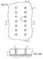
- FIG. 1illustrates a diagrammatic top plan view of a portion of a substrate at a preliminary processing stage according to an embodiment of the present disclosure, showing the substrate with a neutral wetting material thereon.
- FIGS. 1A-1Bare elevational, cross-sectional views of the substrate depicted in FIG. 1 taken along lines 1 A- 1 A and 1 B- 1 B, respectively.
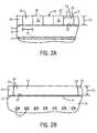
- FIG. 2illustrates a diagrammatic top plan view of the substrate of FIG. 1 at a subsequent stage showing the formation of trenches in a material layer formed on the neutral wetting material.
- FIGS. 2A-2Billustrate elevational, cross-sectional views of a portion of the substrate depicted in FIG. 2 taken, respectively, along lines 2 A- 2 A and 2 B- 2 B.
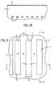
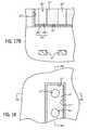
- FIG. 3illustrates a side elevational view of a portion of a substrate at a preliminary processing stage according to another embodiment of the disclosure, showing the substrate with trenches in a material layer formed on the substrate.
- FIG. 4illustrates a side elevational view of the substrate of FIG. 3 at a subsequent stage showing the formation of a neutral wetting material within the trenches.
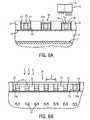
- FIGS. 5-6are diagrammatic top plan views of the substrate of FIG. 2 at subsequent stages in the fabrication of a self-assembled block copolymer film composed of a single row of perpendicular oriented cylinders in a polymer matrix within the trenches according to an embodiment of the disclosure.
- FIGS. 5A-6Aillustrate elevational, cross-sectional views of a portion of the substrate depicted in FIGS. 5-6 taken along lines 5 A- 5 A and 6 A- 6 A, respectively.
- FIGS. 5B-6Bare cross-sectional views of the substrate depicted in FIGS. 5-6 taken along lines 5 B- 5 B and 6 B- 6 B, respectively.
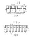
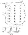
- FIGS. 7-9are top plan views of the substrate of FIG. 6 at subsequent stages, illustrating an embodiment of the use of the self-assembled block copolymer film after removal of one of the polymer blocks, as a mask to etch the substrate and filling of the etched openings.
- FIGS. 7A-9Aillustrate elevational, cross-sectional views of a portion of the substrate depicted in FIGS. 7-9 taken along lines 7 A- 7 A to 9 A- 9 A, respectively.
- FIGS. 7B-9Bare cross-sectional views of the substrate depicted in FIGS. 7-9 taken along lines 7 B- 7 B to 9 B- 9 B, respectively.
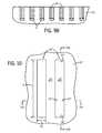
- FIG. 10is a diagrammatic top plan view of a portion of a substrate at a preliminary processing stage according to another embodiment of the disclosure, showing trenches in a material layer exposing the substrate.
- FIGS. 10A-10Bare elevational, cross-sectional views of the substrate depicted in FIG. 10 taken along lines 10 A- 10 A and 10 B- 10 B, respectively.
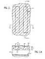
- FIGS. 11-12are diagrammatic top plan views of the substrate of FIG. 10 at subsequent stages in the fabrication of a self-assembled block copolymer film within the trenches in the material layer.
- FIGS. 11A-12Aillustrate elevational, cross-sectional views of a portion of the substrate depicted in FIGS. 11-12 taken along lines 11 A- 11 A and 12 A- 12 A, respectively.
- FIGS. 11B-12Bare cross-sectional views of the substrate depicted in FIGS. 11-12 taken along lines 11 B- 11 B and 12 B- 12 B, respectively.
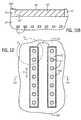
- FIGS. 13-15are top plan views of the substrate of FIG. 12 at subsequent stages, illustrating the use of the self-assembled block copolymer film after removal of one of the polymer blocks, as a mask to etch the substrate and filling of the etched openings according to an embodiment of the disclosure.
- FIGS. 13A-15Aillustrate elevational, cross-sectional views of a portion of the substrate depicted in FIGS. 13-15 taken along lines 13 A- 13 A to 15 A- 15 A, respectively.
- FIGS. 13B-15Bare cross-sectional views of the substrate depicted in FIGS. 13-15 taken along lines 13 B- 13 B to 15 B- 15 B, respectively.
- FIG. 16is a top plan view of a portion of the substrate of FIG. 12 according to another embodiment of the invention, showing a bilayer wetting layer along the trench surfaces.
- FIGS. 16A-16Bare elevational, cross-sectional views of the substrate depicted in FIG. 16 taken along lines 16 A- 16 A and 16 B- 16 B, respectively.
- FIGS. 17-18are top plan views of the substrate of FIG. 16 at subsequent stages, showing the removal of one of the polymer domains to form openings to the substrate according to another embodiment of the invention.
- FIGS. 17A-18Aillustrate elevational, cross-sectional views of a portion of the substrate depicted in FIGS. 17-18 taken along lines 17 A- 17 A to 18 A- 18 A, respectively.
- FIGS. 17B-18Bare cross-sectional views of the substrate depicted in FIGS. 17-18 taken along lines 17 B- 17 B to 18 B- 18 B, respectively.
- FIGS. 19-22illustrate another embodiment of the invention for forming two rows of cylinders in a single trench.
- FIG. 19illustrates a top plan view of a portion of a substrate at a preliminary processing stage showing a trench in a material layer.
- FIGS. 19A-19Bare elevational, cross-sectional views of a portion of the substrate depicted in FIG. 19 taken, respectively, along lines 19 A- 19 A and 19 B- 19 B.
- FIG. 20is a top plan view of the substrate of FIG. 19 at a subsequent stage in the fabrication of a self-assembled cylindrical-phase block copolymer material within the trench according to an embodiment of the invention.
- FIG. 21is a top plan view of the substrate of FIG. 20 at a subsequent stage after removal of the cydrical domains of the block copolymer material.
- FIG. 22is a top plan view of FIG. 21 after etching of the substrate and filling of the etched openings.
- FIGS. 20A-22Aare elevational, cross-sectional views of the substrates of FIGS. 20-22 taken, respectively, along lines 20 A- 20 A, 21 A- 21 A and 22 A- 22 A.
- FIGS. 20B-22Bare elevational, cross-sectional views of the substrates of FIGS. 20-22 , taken along lines 20 B- 20 B, 21 B- 21 B and 22 B- 22 B, respectively, showing both lines of cylinders.
- semiconductor substrateor “semiconductive substrate” or “semiconductive wafer fragment” or “wafer fragment” or “wafer” will be understood to mean any construction comprising semiconductor material, including but not limited to bulk semiconductive materials such as a semiconductor wafer (either alone or in assemblies comprising other materials thereon), and semiconductive material layers (either alone or in assemblies comprising other materials).
- substraterefers to any supporting structure including, but not limited to, the semiconductive substrates, wafer fragments or wafers described above.
- L ois the inherent periodicity or pitch value (bulk period or repeat unit) of structures that self assemble upon annealing from a self-assembling (SA) block copolymer.
- L Bis the periodicity or pitch value of a blend of a block copolymer with one or more of its constituent homopolymers.
- Lis used herein to indicate the center-to-center cylinder pitch or spacing of cylinders of the block copolymer or blend, and is equivalent to “L o ” for a pure block copolymer and “L B ” for a copolymer blend.
- a polymer materiale.g., film, layer
- a polymer materialis prepared by guided self-assembly of block copolymers, with both polymer domains at the air interface.
- Block copolymer materialsspontaneously assemble into periodic structures by microphase separation of the constituent polymer blocks after annealing, forming ordered domains at nanometer-scale dimensions.
- a one-dimensional (1-D) array of perpendicular-oriented cylindersis formed within a trench. In other embodiments, two rows of cylinders can be formed in each trench.
- the pattern of perpendicular-oriented cylinders that is formed on the substratecan then be used, for example, as an etch mask for patterning nanosized features into the underlying substrate through selective removal of one block of the self-assembled block copolymer.
- Ldomain sizes and periods (L) involved in this method are determined by the chain length of a block copolymer (MW)
- resolutioncan exceed other techniques such as conventional photolithography. Processing costs using the technique is significantly less than extreme ultraviolet (EUV) photolithography, which has comparable resolution.
- EUVextreme ultraviolet
- the described embodimentinvolves a thermal anneal of a cylindrical-phase block copolymer in combination with a graphoepitaxy technique that utilizes a lithographically defined trench as a guide with a floor composed of a material that is neutral wetting to both polymer blocks, and sidewalls and ends that are preferential wetting to one polymer block and function as constraints to induce the block copolymer to self-assemble into an ordered 1-D array of a single row of cylinders in a polymer matrix oriented perpendicular to the trench floor and registered to the trench sidewalls.
- two rows of cylinderscan be formed in each trench.
- the block copolymer or blendis constructed such that all of the polymer blocks will have equal preference for the air interface during the anneal.
- diblock copolymersinclude, for example, poly(styrene)-b-poly(methylmethacrylate) (PS-b-PMMA) or other PS-b-poly(acrylate) or PS-b-poly(methacrylate), poly(styrene)-b-poly(lactide) (PS-b-PLA), and poly(styrene)-b-poly(tert-butyl acrylate) (PS-b-PtBA), among others.
- PS-b-PMMApoly(styrene)-b-poly(methylmethacrylate)
- PS-b-PLApoly(styrene)-b-poly(lactide)
- PS-b-PtBApoly(styrene)-b-poly(tert-butyl acrylate)
- a ternary diblock copolymer blendis a PS-b-PMMA/PS/PMMA blend, for example, 60% of 46K/21K PS-b-PMMA, 20% of 20K polystyrene and 20% of 20K poly(methyl methacrylate).
- a blend of PS-PEO and about 0-40% PEO homopolymer (HP)can also be used to produce perpendicular cylinders during a thermal anneal; it is believed that the added PEO homopolymer may function, at least in part, to lower the surface energy of the PEO domains to that of PS.
- An example of a cylinder-forming PS-b-PMMA copolymer material (L o ⁇ 35 nm) to form about 20 nm diameter cylindrical PMMA domains in a matrix of PSis composed of about 70% PS and 30% PMMA with a total molecular weight (M n ) of 67 kg/mol.
- a single trench or multiple trenchescan be formed in the substrate, and can span the entire width of an array of lines (or other active area).
- the substrate 10is provided with an array of conductive lines 12 (or other active areas) at a pitch of L.
- the trench or trenchesare formed over the active areas 12 (e.g., lines) such that when the block copolymer material is annealed, each cylinder will be situated above a single active area 12 (e.g., conductive line).
- multiple trenchesare formed with the ends 24 of each adjacent trench 18 aligned or slightly offset from each other at less than 5% of L such that cylinders in adjacent trenches are aligned and situated above the same line 12 .
- the material layer 16 ′can be formed on the substrate 10 ′, etched to form the trenches 18 ′, and a neutral wetting material 14 ′ can then be formed on the trench floors 26 ′.
- a random copolymer materialcan be deposited into the trenches 18 ′ and crosslinked to form a neutral wetting material layer. Material on surfaces outside the trenches such as on the spacers 20 ′ (e.g., non-crosslinked random copolymer) can be subsequently removed.
- a method called “pitch doubling” or “pitch multiplication”can also be used for extending the capabilities of photolithographic techniques beyond their minimum pitch, as described, for example, in U.S. Pat. No. 5,328,810 (Lowrey et al.), U.S. Pat. No. 7,115,525 (Abatchev, et al.), US 2006/0281266 (Wells) and US 2007/0023805 (Wells).
- the length (l t ) of the trenchesis at or about nL or an integer multiple of L, typically within a range of about n*10 to about n*100 nm (with n being the number of features or structures, e.g., cylinders).
- the depth (D t ) of the trenches 18is greater than L (D t >L).
- the width of the spacers 20 between adjacent trenchescan vary and is generally about L to about nL. In some embodiments, the trench dimension is about 20-100 nm wide (w t ) and about 100-25,000 nm in length (l t ), with a depth (D t ) of about 10-100 nm.
- the block copolymer materialcan be deposited by spin casting (spin-coating) from a dilute solution (e.g., about 0.25-2 wt % solution) of the copolymer in an organic solvent such as dichloroethane (CH 2 Cl 2 ) or toluene, for example. Capillary forces pull excess block copolymer material 28 (e.g., greater than a monolayer) into the trenches 18 . As shown, a thin layer or film 28 a of the block copolymer material can be deposited onto the material layer 16 outside the trenches, e.g., on the spacers 20 . Upon annealing, the thin film 28 a will flow into the trenches leaving a structureless brush layer on the material layer 16 from a top-down perspective.
- a dilute solutione.g., about 0.25-2 wt % solution
- organic solventsuch as dichloroethane (CH 2 Cl 2 ) or toluene
- the material layer 16can be composed of silicon (with native oxide), oxide (e.g., silicon oxide, SiO x ), silicon nitride, silicon oxycarbide, indium tin oxide (ITO), silicon oxynitride, and resist materials such as methacrylate-based resists and polydimethyl glutarimide resists, among other materials, which exhibit preferential wetting toward the PMMA block.
- oxidee.g., silicon oxide, SiO x
- silicon nitridesilicon oxycarbide
- ITOindium tin oxide
- resist materialssuch as methacrylate-based resists and polydimethyl glutarimide resists, among other materials, which exhibit preferential wetting toward the PMMA block.
- the copolymer materialwill self assemble to form a thin interface layer and cylinders of PMMA in a PS matrix.
- a neutral wetting trench floor 26allows both blocks of the copolymer material to wet the floor of the trench.
- a neutral wetting material 14can be provided by applying a neutral wetting polymer (e.g., a neutral wetting random copolymer) onto the substrate 10 , forming the material layer 16 and then etching the trenches to expose the underlying neutral wetting material, as illustrated in FIGS. 2-2B .
- a neutral wetting polymere.g., a neutral wetting random copolymer
- another neutral wetting surface for PS-b-PMMAcan be provided by hydrogen-terminated silicon.
- the floors 26 of the trenches 18can be etched, for example, with a hydrogen plasma, to remove the oxide material and form hydrogen-terminated silicon, which is neutral wetting with equal affinity for both blocks of a block copolymer material.
- H-terminated siliconcan be prepared by a conventional process, for example, by a fluoride ion etch of a silicon substrate (with native oxide present, about 12-15 ⁇ ) by exposure to an aqueous solution of hydrogen fluoride (HF) and buffered HF or ammonium fluoride (NH 4 F), by HF vapor treatment, or by a hydrogen plasma treatment (e.g., atomic hydrogen).
- a fluoride ion etch of a silicon substratewith native oxide present, about 12-15 ⁇
- HFhydrogen fluoride
- NH 4 Fbuffered HF or ammonium fluoride
- HF vapor treatmente.g., atomic hydrogen
- the block copolymer material 28is then thermally annealed (arrows ⁇ ) to cause the polymer blocks to phase separate and self assemble according to the preferential and neutral wetting of the trench surfaces to form a self-assembled polymer material 30 , as illustrated in FIGS. 6-6B .
- Thermal annealingcan be conducted at above the glass transition temperature of the component blocks of the copolymer material.
- a PS-b-PMMA copolymer materialcan be globally annealed at a temperature of about 180-230° C. in a vacuum oven for about 1-24 hours to achieve the self-assembled morphology.
- the copolymer materialcan be treated to crosslink the polymer segments (e.g., the PS segments) to fix and enhance the strength of the self-assembled polymer blocks.
- the polymerscan be structured to inherently crosslink (e.g., upon exposure to ultraviolet (UV) radiation, including deep ultraviolet (DUV) radiation), or one of the polymer blocks of the copolymer material can be formulated to contain a crosslinking agent.
- the annealed polymer material 30can be crosslinked globally, a photoresist material can be applied to pattern and expose the areas of the polymer material 28 a outside the trench regions, and the exposed portions of the polymer material 28 a can be removed, for example by an oxygen (O 2 ) plasma treatment.
- O 2oxygen
- An application of the self-assembled polymer material 30is as an etch mask to form openings in the substrate 10 .
- the cylindrical polymer domains 34 of the self-assembled polymer material 30can be selectively removed resulting in a polymer matrix 36 with openings 40 exposing the trench floor.
- PMMA domainscan be selectively removed by UV exposure/acetic acid development or by selective reactive ion etching (RIE). The remaining porous polymer (e.g.
- the residual matrix 36can be removed and the substrate openings 42 can be filled with a material 44 such as a metal or metal alloy such as Cu, Al, W, Si, and Ti 3 N 4 , among others, to form arrays of cylindrical contacts to the conductive lines 12 .
- the cylindrical openings 42 in the substratecan also be filled with a metal-insulator-metal stack to form capacitors with an insulating material such as SiO 2 , Al 2 O 3 , HfO 2 , ZrO 2 , SrTiO 3 , and the like.
- PS-b-PMMA block copolymer doped with PEO-coated gold nanoparticles of a size less than the diameter of the self-assembled cylindersPark et al, Macromolecules, 2007, 40(11), 8119-8124
- PS-b-PMMApoly(styrene)-b-poly(methylmethacrylate)
- PS-b-PMMApoly(styrene)-b-poly(methylmethacrylate)
- PS-b-PMMApoly(styrene)-b-poly(methylmethacrylate)
- PS-b-PMMApoly(styrene)-b-poly(methylmethacrylate)
- PS-b-PMMApoly(styrene)-b-poly(acrylate) or PS-b-poly(methacrylate)
- PS-b-PLApoly(styrene)-b-poly(vinylpyridine)
- PS-b-PVPpoly(styrene
- triblock copolymersexamples include ABC polymers such as poly(styrene-b-methyl methacrylate-b-ethylene oxide) (PS-b-PMMA-b-PEO), and ABA copolymers such as PS-b-PI-b-PS.
- ABC polymerssuch as poly(styrene-b-methyl methacrylate-b-ethylene oxide) (PS-b-PMMA-b-PEO)
- ABA copolymerssuch as PS-b-PI-b-PS.
- a substrate 10 ′′is shown with conductive lines 12 ′′ (or other active area) and an overlying material layer 16 ′′ in which trenches 18 ′′ have been etched.
- the substrate 10 ′′ and material layer 16 ′′ defining the trench surfacescan be a material that is inherently preferential wetting to one of the polymer blocks, or in other embodiments, a preferential wetting material can be applied onto the surfaces of the trenches.
- a cylindrical-phase PS-b-PEO block copolymer material 28 ′′ (or blend with homopolymers) having an inherent pitch at or about Lcan be deposited into the trenches 18 ′′, as shown in FIGS. 11-11B .
- the thickness (t 1 ) of the block copolymer material deposited into the trenchcan be about the L value of the material or greater, e.g., up to about 1000% of the L value.
- the volume fractions of the two blocks (AB) of the PS-b-PEO diblock copolymerare generally at a ratio of about 60:40 and 80:20, such that the block copolymer will microphase separate and self-assemble into cylindrical domains of polymer B (i.e., PEO) within a matrix of polymer A (i.e., PS).
- diblock copolymersare used in the illustrative embodiment, triblock or multiblock copolymers can also be used.
- the PS-b-PEO block copolymer materialcan also be formulated as a binary or ternary blend comprising a PS-b-PEO block copolymer and one or more homopolymers (i.e., polystyrene (PS) and polyethylene oxide (PEO) to produce blends that swell the size of the polymer domains and increase the L value of the polymer.
- the volume fraction of the homopolymerscan range from 0 to about 40%.
- An example of a ternary diblock copolymer blendis a PS-b-PEO/PS/PEO blend.
- the L value of the polymercan also be modified by adjusting the molecular weight of the block copolymer.
- the block copolymer materialis swollen by exposure to a vapor of a “good” solvent for both blocks, for example, benzene, chloroform or a chloroform/octane mixture.
- the block copolymer material 28 ′′is exposed to the solvent vapors to slowly swell both polymer blocks (PS, PEO) of the material.
- PS, PEOpolymer blocks
- the solvent and solvent vaporsare then allowed to slowly diffuse out of the swollen polymer material and evaporate.
- the solvent-saturated vapormaintains a neutral air interface 46 ′′ with the copolymer material 28 ′′, which induces the formation of perpendicular features throughout the copolymer material.
- a solvent annealcan be conducted in high humidity (e.g., about 70-85%) with water condensation on the film, which cools as the solvent (e.g., benzene) evaporates.
- the cylindershave a diameter at or about 0.5*L (e.g., about one-half of the center-to-center distance between cylinders), the number (n) of cylinders in the row is according to the length (l t ) of the trench, and the center-to-center distance (pitch distance, p) between cylinder domains is at or about L.
- Removal of the PEO phase domains 34 ′′can be performed, for example, by exposure of the self-assembled block copolymer material 30 ′′ (optionally cross-linked) to aqueous hydroiodic acid or exposure to water alone, which will draw PEO to the surface without cleaving the bonds to the PS domains.
- the PS-b-PEO block copolymerincludes an acid-cleavable linker (e.g., trityl alcohol linker) positioned between the polymer blocks
- exposure of the crosslinked polymer material 30 ′′ to an aqueous acid (e.g., trifluoroacetic acid) or to an acid vaporcan be performed to cleave the polymer into PEO and PS fragments (S.
- Rinsing with watercan then be performed to remove the cleaved PEO domains 34 ′′.
- exposure to water to draw the PEO domains to the surface followed by a brief oxygen (O 2 ) plasma etchcan also be performed to remove the PEO domains.
- the substrate 10 ′′ and material layer 16 ′′can be formed from a material that is inherently preferential wetting to the PLA block, or in other embodiments, a preferential wetting material can be applied onto the surfaces of the trenches 18 ′′, with the same or closely similar material being used to define the sidewalls 22 ′′, ends 24 ′′ and floor 26 ′′ of the trenches.
- a cylindrical-phase PS-b-PLA block copolymer material 28 ′′(or triblock or multiblock copolymers or blend with homopolymers) having an inherent pitch at or about L can be deposited into the trenches 18 ′′, as shown in FIGS. 11-11B .
- both polymer blockse.g., PLA and PS
- the minority (e.g., PLA) blockwill preferentially wet the surfaces 22 ′′, 24 ′′ 26 ′′ of the trench to form a thin wetting layer 34 a ′′ on each of the trench surfaces as illustrated in FIGS. 12-12B .
- the wetting layer 34 a ′′′is a bilayer of PLA 48 a ′′′ and PS 48 b ′′′.
- the PS 48 b ′′′ portion of the wetting layer(depicted with broken lining - - - ) is continuous with the overall PS matrix 36 ′′′, as shown.
- Thermal annealing of the block copolymer material 28 ′′′ in combination with the constraints provided by the width (w t ) of the trench 18 ′′′, the preferential wetting trench surfaces 22 ′′′, 24 ′′′ 26 ′′′ and the composition of the block copolymercauses the minority polymer block (e.g., PLA block) to self assemble to form perpendicular-oriented cylindrical domains 34 ′′′ in a single row within a matrix 36 ′′′ of the majority polymer block (e.g., PS), with the PLA 48 a ′′′/PS 48 b ′′′ bilayer along the trench surfaces 22 ′′′, 24 ′′′, 26 ′′′.
- the minority polymer blocke.g., PLA block
- the block copolymer material 28 ′′′can be “zone annealed” as previously described.
- the PLA cylindrical domains 34 ′′′extend from the air interface 46 ′′′ to the wetting layer 34 a ′′′ composed of the PLA/PS bilayer 48 a ′′′/ 48 b ′′′ overlying the surface of the substrate 10 ′′′ at the trench floor 26 ′′′.
- the PS layer 48 b ′′′which is covalently bonded to the PLA layer 48 a ′′′, is in contact with the PS block (matrix 26 ′′′), which in turn is covalently bonded to the PLA cylinder domains 34 ′′′.
- the matrix 30 ′′can then be used as a mask to etch cylindrical-shaped openings 42 ′′ in the substrate down to an active area such as a conductive line 12 ′′ or to semi-conducting regions, etc.
- the remnants of the etch mask 36 ′′can be subsequently removed and the openings 42 ′′ can be filled as desired, as described with respect to FIGS. 15-15B .
- the trenchesare constructed with a width (w t ) of about 1.75-2.5*L of the block copolymer such that, upon annealing, a block copolymer material or blend of about L will self-assemble into two rows of perpendicular cylinders with each cylinder being offset to form a zigzag pattern, and the center-to-center pitch distance between adjacent cylinders at or about one-half L ( ⁇ 0.5*L).
- w twidth of about 1.75-2.5*L of the block copolymer such that, upon annealing, a block copolymer material or blend of about L will self-assemble into two rows of perpendicular cylinders with each cylinder being offset to form a zigzag pattern, and the center-to-center pitch distance between adjacent cylinders at or about one-half L ( ⁇ 0.5*L).
- the ends 24 ′′′′can be angled or beveled as depicted by the dashed line 50 in FIG. 20 .
- the dimensions of the trench 18 ′′′′can be, for example, about 70-100 nm wide (w t ), about 100-25,000 nm long (l t ), and about 40-200 nm deep (D t ).
- the trench 18 ′′′′is fabricated with the appropriate neutral or preferential wetting surface on the sidewalls 22 ′′′′, ends 24 ′′′′, and trench floor 26 ′′′′, to drive the block copolymer to self-assemble into perpendicular-oriented cylinders 34 ′′′′ upon annealing, as depicted in FIGS. 20-20B .
- the resulting cylinders 34 ′′′′are formed in a staggered two-row arrangement parallel to the sidewalls 22 ′′′′ in which the center-to-center pitch distance (p) of adjacent cylinders 34 ′′′′ within a row is at or about 0.5*L.
- FIG. 20Billustrates a schematic cross-sectional, elevational view of both rows of cylinders in relation to the underlying lines 12 ′′′′.
- the self-assembled polymer filmcan then be processed to form a mask ( FIGS. 21-21B ) by removing the cylinder domains 34 ′′′′ (e.g., PMMA) leaving a polymer matrix 36 ′′′′ (e.g., PS) with cylindrical openings 40 ′′′′ to the underlying substrate 10 ′′′′, which can then be etched to form openings 42 ′′′′ (shown in phantom) to “buried” active areas (e.g., lines 12 ′′′′) and the openings 42 ′′′′ can then be filled ( FIGS. 22-22B ) with a desired material 44 ′′′′, e.g., metal, to form, for example, a contact to underlying lines 12 ′′′′.
- a desired material 44 ′′′′e.g., metal
- Methods of the disclosureprovide a means of generating self-assembled diblock copolymer films composed of perpendicular-oriented cylinders in a polymer matrix.
- the methodsprovide ordered and registered elements on a nanometer scale that can be prepared more inexpensively than by electron beam lithography, EUV photolithography or conventional photolithography.
- the feature sizes produced and accessible by this inventioncannot be easily prepared by conventional photolithography.
- the described methods and systemscan be readily employed and incorporated into existing semiconductor manufacturing process flows and provide a low cost, high-throughput technique for fabricating small structures.
Landscapes
- Engineering & Computer Science (AREA)
- Chemical & Material Sciences (AREA)
- Physics & Mathematics (AREA)
- General Physics & Mathematics (AREA)
- Manufacturing & Machinery (AREA)
- Condensed Matter Physics & Semiconductors (AREA)
- Microelectronics & Electronic Packaging (AREA)
- Power Engineering (AREA)
- Computer Hardware Design (AREA)
- Nanotechnology (AREA)
- Inorganic Chemistry (AREA)
- Analytical Chemistry (AREA)
- Composite Materials (AREA)
- Materials Engineering (AREA)
- Crystallography & Structural Chemistry (AREA)
- Exposure Of Semiconductors, Excluding Electron Or Ion Beam Exposure (AREA)
- Formation Of Insulating Films (AREA)
- Semiconductor Memories (AREA)
- Drying Of Semiconductors (AREA)
- Micromachines (AREA)
- Manufacture Of Macromolecular Shaped Articles (AREA)
- Graft Or Block Polymers (AREA)
Abstract
Description
Claims (48)
Priority Applications (7)
| Application Number | Priority Date | Filing Date | Title |
|---|---|---|---|
| US12/030,562US8101261B2 (en) | 2008-02-13 | 2008-02-13 | One-dimensional arrays of block copolymer cylinders and applications thereof |
| KR1020107020026AKR101262460B1 (en) | 2008-02-13 | 2009-01-27 | One-dimensional arrays of block copolymer cylinders and applications thereof |
| CN2009801050240ACN101952195B (en) | 2008-02-13 | 2009-01-27 | One-dimensional arrays of block copolymer cylinders and applications thereof |
| EP09711291AEP2262721A2 (en) | 2008-02-13 | 2009-01-27 | One-dimensional arrays of block copolymer cylinders and applications thereof |
| PCT/US2009/032130WO2009102551A2 (en) | 2008-02-13 | 2009-01-27 | One-dimensional arrays of block copolymer cylinders and applications thereof |
| TW098104203ATWI462871B (en) | 2008-02-13 | 2009-02-10 | One-dimensional arrays of block copolymer cylinders and applications thereof |
| US13/312,383US8642157B2 (en) | 2008-02-13 | 2011-12-06 | One-dimensional arrays of block copolymer cylinders and applications thereof |
Applications Claiming Priority (1)
| Application Number | Priority Date | Filing Date | Title |
|---|---|---|---|
| US12/030,562US8101261B2 (en) | 2008-02-13 | 2008-02-13 | One-dimensional arrays of block copolymer cylinders and applications thereof |
Related Child Applications (1)
| Application Number | Title | Priority Date | Filing Date |
|---|---|---|---|
| US13/312,383ContinuationUS8642157B2 (en) | 2008-02-13 | 2011-12-06 | One-dimensional arrays of block copolymer cylinders and applications thereof |
Publications (2)
| Publication Number | Publication Date |
|---|---|
| US20090200646A1 US20090200646A1 (en) | 2009-08-13 |
| US8101261B2true US8101261B2 (en) | 2012-01-24 |
Family
ID=40938191
Family Applications (2)
| Application Number | Title | Priority Date | Filing Date |
|---|---|---|---|
| US12/030,562Active2029-05-28US8101261B2 (en) | 2008-02-13 | 2008-02-13 | One-dimensional arrays of block copolymer cylinders and applications thereof |
| US13/312,383ActiveUS8642157B2 (en) | 2008-02-13 | 2011-12-06 | One-dimensional arrays of block copolymer cylinders and applications thereof |
Family Applications After (1)
| Application Number | Title | Priority Date | Filing Date |
|---|---|---|---|
| US13/312,383ActiveUS8642157B2 (en) | 2008-02-13 | 2011-12-06 | One-dimensional arrays of block copolymer cylinders and applications thereof |
Country Status (6)
| Country | Link |
|---|---|
| US (2) | US8101261B2 (en) |
| EP (1) | EP2262721A2 (en) |
| KR (1) | KR101262460B1 (en) |
| CN (1) | CN101952195B (en) |
| TW (1) | TWI462871B (en) |
| WO (1) | WO2009102551A2 (en) |
Cited By (31)
| Publication number | Priority date | Publication date | Assignee | Title |
|---|---|---|---|---|
| US20100155690A1 (en)* | 2008-12-18 | 2010-06-24 | Stmicroelectronics S.R.L. | Cross-point cell nanoarray with anisotropic active organic layer |
| US20120076978A1 (en)* | 2008-02-13 | 2012-03-29 | Millward Dan B | One-Dimensional Arrays of Block Copolymer Cylinders and Applications Thereof |
| US20120094087A1 (en)* | 2007-03-06 | 2012-04-19 | Millward Dan B | Registered Structure Formation via the Application of Directed Thermal Energy to Diblock Copolymer Films |
| US20120141741A1 (en)* | 2008-04-21 | 2012-06-07 | Millward Dan B | Multi-Layer Method for Formation of Registered Arrays of Cylindrical Pores in Polymer Films |
| US8445592B2 (en) | 2007-06-19 | 2013-05-21 | Micron Technology, Inc. | Crosslinkable graft polymer non-preferentially wetted by polystyrene and polyethylene oxide |
| US8450418B2 (en) | 2010-08-20 | 2013-05-28 | Micron Technology, Inc. | Methods of forming block copolymers, and block copolymer compositions |
| WO2013119820A1 (en) | 2012-02-10 | 2013-08-15 | Board Of Regents, The University Of Texas System | Polyactide/silicon-containing block copolymers for nanolithography |
| US8518275B2 (en) | 2008-05-02 | 2013-08-27 | Micron Technology, Inc. | Graphoepitaxial self-assembly of arrays of downward facing half-cylinders |
| US8551808B2 (en) | 2007-06-21 | 2013-10-08 | Micron Technology, Inc. | Methods of patterning a substrate including multilayer antireflection coatings |
| US8557128B2 (en) | 2007-03-22 | 2013-10-15 | Micron Technology, Inc. | Sub-10 nm line features via rapid graphoepitaxial self-assembly of amphiphilic monolayers |
| US8609221B2 (en) | 2007-06-12 | 2013-12-17 | Micron Technology, Inc. | Alternating self-assembling morphologies of diblock copolymers controlled by variations in surfaces |
| US8633112B2 (en) | 2008-03-21 | 2014-01-21 | Micron Technology, Inc. | Thermal anneal of block copolymer films with top interface constrained to wet both blocks with equal preference |
| US8641914B2 (en) | 2008-03-21 | 2014-02-04 | Micron Technology, Inc. | Methods of improving long range order in self-assembly of block copolymer films with ionic liquids |
| US8669645B2 (en) | 2008-10-28 | 2014-03-11 | Micron Technology, Inc. | Semiconductor structures including polymer material permeated with metal oxide |
| US8900963B2 (en) | 2011-11-02 | 2014-12-02 | Micron Technology, Inc. | Methods of forming semiconductor device structures, and related structures |
| US8956713B2 (en) | 2007-04-18 | 2015-02-17 | Micron Technology, Inc. | Methods of forming a stamp and a stamp |
| US8999492B2 (en) | 2008-02-05 | 2015-04-07 | Micron Technology, Inc. | Method to produce nanometer-sized features with directed assembly of block copolymers |
| US8999623B2 (en) | 2013-03-14 | 2015-04-07 | Wiscousin Alumni Research Foundation | Degradable neutral layers for block copolymer lithography applications |
| US9087699B2 (en) | 2012-10-05 | 2015-07-21 | Micron Technology, Inc. | Methods of forming an array of openings in a substrate, and related methods of forming a semiconductor device structure |
| US9142420B2 (en) | 2007-04-20 | 2015-09-22 | Micron Technology, Inc. | Extensions of self-assembled structures to increased dimensions via a “bootstrap” self-templating method |
| US9177795B2 (en) | 2013-09-27 | 2015-11-03 | Micron Technology, Inc. | Methods of forming nanostructures including metal oxides |
| US9229328B2 (en) | 2013-05-02 | 2016-01-05 | Micron Technology, Inc. | Methods of forming semiconductor device structures, and related semiconductor device structures |
| US9627202B2 (en) | 2014-08-11 | 2017-04-18 | Samsung Electronics Co., Ltd. | Methods for forming fine patterns of semiconductor device |
| US9765214B2 (en) | 2015-02-26 | 2017-09-19 | The Regents Of The University Of California | Copolymer formulation for directed self-assembly, methods of manufacture thereof and articles comprising the same |
| US9772554B2 (en) | 2015-02-26 | 2017-09-26 | Dow Global Technologies Llc | Copolymer formulation for directed self-assembly, methods of manufacture thereof and articles comprising the same |
| US9840637B2 (en) | 2015-02-26 | 2017-12-12 | Dow Global Technologies Llc | Copolymer formulation for directed self-assembly, methods of manufacture thereof and articles comprising the same |
| US10011713B2 (en) | 2014-12-30 | 2018-07-03 | Dow Global Technologies Llc | Copolymer formulation for directed self assembly, methods of manufacture thereof and articles comprising the same |
| US10056265B2 (en) | 2016-03-18 | 2018-08-21 | Taiwan Semiconductor Manufacturing Co., Ltd. | Directed self-assembly process with size-restricted guiding patterns |
| US10294359B2 (en) | 2014-12-30 | 2019-05-21 | Rohm And Haas Electronic Materials Llc | Copolymer formulation for directed self assembly, methods of manufacture thereof and articles comprising the same |
| US10351727B2 (en) | 2015-02-26 | 2019-07-16 | Dow Global Technologies Llc | Copolymer formulation for directed self-assembly, methods of manufacture thereof and articles comprising the same |
| US11021630B2 (en) | 2014-12-30 | 2021-06-01 | Rohm And Haas Electronic Materials Llc | Copolymer formulation for directed self assembly, methods of manufacture thereof and articles comprising the same |
Families Citing this family (51)
| Publication number | Priority date | Publication date | Assignee | Title |
|---|---|---|---|---|
| US8394483B2 (en) | 2007-01-24 | 2013-03-12 | Micron Technology, Inc. | Two-dimensional arrays of holes with sub-lithographic diameters formed by block copolymer self-assembly |
| US7767099B2 (en)* | 2007-01-26 | 2010-08-03 | International Business Machines Corporaiton | Sub-lithographic interconnect patterning using self-assembling polymers |
| JP2010115832A (en)* | 2008-11-12 | 2010-05-27 | Panasonic Corp | Method for promoting self-formation of block copolymer and method for forming self-formation pattern of block copolymer using the method for promoting self-formation |
| US8361704B2 (en)* | 2009-01-12 | 2013-01-29 | International Business Machines Corporation | Method for reducing tip-to-tip spacing between lines |
| US8398868B2 (en)* | 2009-05-19 | 2013-03-19 | International Business Machines Corporation | Directed self-assembly of block copolymers using segmented prepatterns |
| US8114306B2 (en)* | 2009-05-22 | 2012-02-14 | International Business Machines Corporation | Method of forming sub-lithographic features using directed self-assembly of polymers |
| TWI404753B (en)* | 2009-07-03 | 2013-08-11 | Nat Univ Tsing Hua | Fabrication method of nanomaterials using block copolymer templates |
| WO2011094597A2 (en)* | 2010-02-01 | 2011-08-04 | The Regents Of The University Of California | Graphene nanomesh and method of making the same |
| US8486611B2 (en) | 2010-07-14 | 2013-07-16 | Micron Technology, Inc. | Semiconductor constructions and methods of forming patterns |
| JP5300799B2 (en)* | 2010-07-28 | 2013-09-25 | 株式会社東芝 | Pattern forming method and polymer alloy base material |
| US8232211B1 (en)* | 2011-01-20 | 2012-07-31 | International Business Machines Corporation | Methods for self-aligned self-assembled patterning enhancement |
| KR20120126725A (en)* | 2011-05-12 | 2012-11-21 | 에스케이하이닉스 주식회사 | Method for forming semiconductor device |
| WO2013028308A1 (en) | 2011-08-22 | 2013-02-28 | Dow Global Technologies Llc | Composite membrane formed from polymer blend including self-assembling block copolymers |
| CN102320557A (en)* | 2011-09-08 | 2012-01-18 | 中国科学院研究生院 | Method for preparing metal nanometer particles with hexagonal network in lattice distribution on substrate |
| CN103094095B (en)* | 2011-10-28 | 2015-10-21 | 中芯国际集成电路制造(北京)有限公司 | Manufacture the method for semiconductor device |
| CN103187245B (en)* | 2011-12-30 | 2015-06-17 | 中芯国际集成电路制造(上海)有限公司 | Method of photoetching of block copolymer through directed self-assembly |
| CN104159657B (en) | 2012-02-21 | 2017-05-10 | 陶氏环球技术有限责任公司 | Composite membrane |
| JP5891075B2 (en)* | 2012-03-08 | 2016-03-22 | 東京応化工業株式会社 | Block copolymer-containing composition and pattern reduction method |
| US9005877B2 (en) | 2012-05-15 | 2015-04-14 | Tokyo Electron Limited | Method of forming patterns using block copolymers and articles thereof |
| JP5835123B2 (en)* | 2012-06-21 | 2015-12-24 | Jsr株式会社 | Self-assembling composition for pattern formation and pattern forming method |
| JP6239813B2 (en) | 2012-07-18 | 2017-11-29 | 株式会社Screenセミコンダクターソリューションズ | Substrate processing apparatus and substrate processing method |
| JP2014033051A (en)* | 2012-08-02 | 2014-02-20 | Toshiba Corp | Method for forming pattern and method for manufacturing semiconductor device |
| US8894869B2 (en)* | 2012-11-13 | 2014-11-25 | Taiwan Semiconductor Manufacturing Company, Ltd. | Lithography process using directed self assembly |
| EP2733533B1 (en)* | 2012-11-14 | 2018-02-28 | IMEC vzw | Etching method using block-copolymers |
| KR101993255B1 (en)* | 2013-01-07 | 2019-06-26 | 삼성전자주식회사 | Method of forming contact holes |
| US9312220B2 (en) | 2013-03-12 | 2016-04-12 | Taiwan Semiconductor Manufacturing Company, Ltd. | Structure and method for a low-K dielectric with pillar-type air-gaps |
| US8980538B2 (en) | 2013-03-14 | 2015-03-17 | Tokyo Electron Limited | Chemi-epitaxy in directed self-assembly applications using photo-decomposable agents |
| US8975009B2 (en) | 2013-03-14 | 2015-03-10 | Tokyo Electron Limited | Track processing to remove organic films in directed self-assembly chemo-epitaxy applications |
| US20140273534A1 (en) | 2013-03-14 | 2014-09-18 | Tokyo Electron Limited | Integration of absorption based heating bake methods into a photolithography track system |
| US9147574B2 (en) | 2013-03-14 | 2015-09-29 | Tokyo Electron Limited | Topography minimization of neutral layer overcoats in directed self-assembly applications |
| US9136110B2 (en) | 2013-03-15 | 2015-09-15 | Tokyo Electron Limited | Multi-step bake apparatus and method for directed self-assembly lithography control |
| CN103408783A (en)* | 2013-04-24 | 2013-11-27 | 南京工业大学 | Preparation method of porous membrane with regular vertical pore channels |
| WO2015018590A1 (en)* | 2013-08-06 | 2015-02-12 | Asml Netherlands B.V. | Method of designing lithography features by self-assembly of block copolymer |
| KR102394998B1 (en) | 2013-09-04 | 2022-05-04 | 도쿄엘렉트론가부시키가이샤 | Uv-assisted stripping of hardened photoresist to create chemical templates for directed self-assembly |
| US9625815B2 (en)* | 2013-09-27 | 2017-04-18 | Intel Corporation | Exposure activated chemically amplified directed self-assembly (DSA) for back end of line (BEOL) pattern cutting and plugging |
| US9793137B2 (en) | 2013-10-20 | 2017-10-17 | Tokyo Electron Limited | Use of grapho-epitaxial directed self-assembly applications to precisely cut logic lines |
| US9349604B2 (en) | 2013-10-20 | 2016-05-24 | Tokyo Electron Limited | Use of topography to direct assembly of block copolymers in grapho-epitaxial applications |
| KR102066301B1 (en)* | 2013-11-25 | 2020-01-14 | 도쿄엘렉트론가부시키가이샤 | Pattern forming method and heating apparatus |
| US9184058B2 (en)* | 2013-12-23 | 2015-11-10 | Micron Technology, Inc. | Methods of forming patterns by using a brush layer and masks |
| FR3021321B1 (en)* | 2014-05-26 | 2016-06-03 | Commissariat Energie Atomique | METHOD OF REALIZING PATTERNS BY SELF-ASSEMBLING BLOCK COPOLYMERS |
| US10410914B2 (en)* | 2014-05-28 | 2019-09-10 | Asml Netherlands B.V. | Methods for providing lithography features on a substrate by self-assembly of block copolymers |
| US9385129B2 (en)* | 2014-11-13 | 2016-07-05 | Tokyo Electron Limited | Method of forming a memory capacitor structure using a self-assembly pattern |
| KR102335109B1 (en)* | 2014-12-15 | 2021-12-03 | 삼성전자 주식회사 | Method of forming fine pattern and method of manufacturing integrated circuit device using the same |
| US9305834B1 (en)* | 2014-12-30 | 2016-04-05 | GlobalFoundries, Inc. | Methods for fabricating integrated circuits using designs of integrated circuits adapted to directed self-assembly fabrication to form via and contact structures |
| US20160186001A1 (en)* | 2014-12-30 | 2016-06-30 | Rohm And Haas Electronic Materials Llc | Copolymer formulation for directed self assembly, methods of manufacture thereof and articles comprising the same |
| CN104598679B (en)* | 2015-01-14 | 2018-01-26 | 中国石油大学(华东) | A preparation method of self-assembled nano-scroll structure and its simulation verification method |
| KR102402958B1 (en)* | 2015-11-11 | 2022-05-27 | 삼성전자주식회사 | Methods of forming patterns of semiconductor devices and methods of manufacturing semiconductor devices |
| US9947597B2 (en) | 2016-03-31 | 2018-04-17 | Tokyo Electron Limited | Defectivity metrology during DSA patterning |
| CN109153758B (en)* | 2016-06-16 | 2021-04-27 | 株式会社Lg化学 | amphiphilic triblock polymers |
| KR102308953B1 (en)* | 2017-03-10 | 2021-10-05 | 주식회사 엘지화학 | Preparation method of patterened substrate |
| CN108231984A (en)* | 2018-01-31 | 2018-06-29 | 华南理工大学 | Perovskite patterning diaphragm that a kind of phase separation means are realized and preparation method thereof |
Citations (142)
| Publication number | Priority date | Publication date | Assignee | Title |
|---|---|---|---|---|
| US4623674A (en) | 1985-06-21 | 1986-11-18 | Union Carbide Corporation | Polymer/polyols of substituted styrenes and polyurethanes made therefrom |
| US4877647A (en) | 1986-04-17 | 1989-10-31 | Kansas State University Research Foundation | Method of coating substrates with solvated clusters of metal particles |
| US5482656A (en) | 1993-03-04 | 1996-01-09 | Kabushiki Kaisha Toshiba | Non-linear optical devices employing a polysilane composition and a polysilane composition therefor |
| US5538655A (en) | 1994-06-29 | 1996-07-23 | Arthur D. Little, Inc. | Molecular complexes for use as electrolyte components |
| US5622668A (en) | 1992-02-07 | 1997-04-22 | The United States Of America As Represented By The Secretary Of The Air Force | Method for preparing oriented polymer structures and said structures |
| US5904824A (en) | 1997-03-07 | 1999-05-18 | Beckman Instruments, Inc. | Microfluidic electrophoresis device |
| US5948470A (en) | 1997-04-28 | 1999-09-07 | Harrison; Christopher | Method of nanoscale patterning and products made thereby |
| EP0784543B1 (en) | 1995-08-04 | 2000-04-26 | International Business Machines Corporation | Lithographic surface or thin layer modification |
| US6111323A (en) | 1997-12-30 | 2000-08-29 | International Business Machines Corporation | Reworkable thermoplastic encapsulant |
| US6143647A (en) | 1997-07-24 | 2000-11-07 | Intel Corporation | Silicon-rich block copolymers to achieve unbalanced vias |
| US6368871B1 (en) | 1997-08-13 | 2002-04-09 | Cepheid | Non-planar microstructures for manipulation of fluid samples |
| US6403382B1 (en) | 1998-12-08 | 2002-06-11 | Regents Of The University Of Minnesota | Attachment chemistry for organic molecules to silicon |
| US6423465B1 (en) | 2000-01-28 | 2002-07-23 | International Business Machines Corporation | Process for preparing a patterned continuous polymeric brush on a substrate surface |
| US6503841B1 (en) | 2000-07-07 | 2003-01-07 | Agere Systems Inc. | Oxide etch |
| US6506660B2 (en) | 2000-11-15 | 2003-01-14 | International Business Machines Corporation | Semiconductor with nanoscale features |
| US6548830B1 (en) | 1996-05-22 | 2003-04-15 | Sony Corporation | Semiconductor device formed of single crystal grains in a grid pattern |
| US20030077452A1 (en) | 2001-07-17 | 2003-04-24 | Guire Patrick E. | Self assembling monolayer compositions |
| US20030091752A1 (en) | 2001-10-05 | 2003-05-15 | Nealey Paul F. | Guided self-assembly of block copolymer films on interferometrically nanopatterned substrates |
| US6565763B1 (en) | 1999-06-07 | 2003-05-20 | Kabushiki Kaisha Toshiba | Method for manufacturing porous structure and method for forming pattern |
| US6566248B1 (en) | 2001-01-11 | 2003-05-20 | Advanced Micro Devices, Inc. | Graphoepitaxial conductor cores in integrated circuit interconnects |
| US6569528B2 (en) | 2001-06-23 | 2003-05-27 | Pacific Corporation | Amphiphilic biodegradable block copolymers and self-assembled polymer aggregates formed from the same in aqueous milieu |
| US20030100822A1 (en) | 2001-09-01 | 2003-05-29 | Seok Lew | Analyte measuring biosensor chip using image scanning system |
| US20030180966A1 (en) | 2002-03-20 | 2003-09-25 | Wisconsin Alumni Research Foundation | Optical imaging of nanostructured substrates |
| US20030185741A1 (en) | 2001-04-06 | 2003-10-02 | Krzysztof Matyjaszewski | Process for the preparation of nanostructured materials |
| US6699797B1 (en) | 2002-12-17 | 2004-03-02 | Intel Corporation | Method of fabrication of low dielectric constant porous metal silicate films |
| US6713238B1 (en) | 1998-10-09 | 2004-03-30 | Stephen Y. Chou | Microscale patterning and articles formed thereby |
| EP1416303A2 (en) | 2002-10-30 | 2004-05-06 | Hitachi, Ltd. | Functioning substrate with a group of columnar micro pillars and its manufacturing method |
| US20040084298A1 (en) | 2002-10-31 | 2004-05-06 | Y.D. Yao | Fabrication of nanocomposite thin films for high density magnetic recording media |
| US20040127001A1 (en) | 2002-12-27 | 2004-07-01 | International Business Machines Corporation | Robust ultra-low k interconnect structures using bridge-then-metallization fabrication sequence |
| US20040124092A1 (en) | 2002-12-30 | 2004-07-01 | Black Charles T. | Inorganic nanoporous membranes and methods to form same |
| US20040142578A1 (en) | 2002-03-28 | 2004-07-22 | Ulrich Wiesner | Thin film nanostructures |
| US6781166B2 (en) | 1999-07-02 | 2004-08-24 | President & Fellows Of Harvard College | Nanoscopic wire-based devices and arrays |
| US20040192013A1 (en) | 2003-03-31 | 2004-09-30 | Ryu Myung Kwan | Method for fabricating single crystal silicon film |
| US20040222415A1 (en) | 2003-03-11 | 2004-11-11 | Industrial Technology Research Institute | Organic device including semiconducting layer aligned according to microgrooves of photoresist layer |
| US20040254317A1 (en) | 2003-06-12 | 2004-12-16 | Jinlian Hu | Methods for producing di-block polymers |
| US20040256615A1 (en) | 2001-07-09 | 2004-12-23 | Henning Sirringhaus | Lamellar polymer architecture |
| US20040256662A1 (en) | 2003-06-20 | 2004-12-23 | International Business Machines Corporation | Nonvolatile memory device using semiconductor nanocrystals and method of forming same |
| US20040265548A1 (en) | 2003-05-20 | 2004-12-30 | Rong-Ming Ho | Nanopatterned templates from oriented degradable diblock copolymer thin films |
| CN1562730A (en) | 2004-03-24 | 2005-01-12 | 哈尔滨工业大学 | Method for adjusting and controlling configuration of self-assembling block copolymer template oriented to nano micro machining |
| JP2005008882A (en) | 1999-06-07 | 2005-01-13 | Toshiba Corp | Porous structure manufacturing method, porous structure forming material, pattern forming method, pattern forming material, electrochemical cell, and hollow fiber filter |
| TW200511364A (en) | 2003-02-12 | 2005-03-16 | Nantero Inc | Devices having horizontally-disposed nanofabric articles and methods of making the same |
| US20050062165A1 (en) | 2003-09-19 | 2005-03-24 | International Business Machines Corporation | Method of forming closed air gap interconnects and structures formed thereby |
| US20050074706A1 (en) | 2003-10-06 | 2005-04-07 | Robert Bristol | Enhancing photoresist performance using electric fields |
| US6890703B2 (en) | 2002-03-06 | 2005-05-10 | International Business Machines Corporation | Preparation of crosslinked particles from polymers having activatible crosslinking groups |
| US6890624B1 (en) | 2000-04-25 | 2005-05-10 | Nanogram Corporation | Self-assembled structures |
| US20050100830A1 (en) | 2003-10-27 | 2005-05-12 | Molecular Imprints, Inc. | Methods for fabricating patterned features utilizing imprint lithography |
| US20050124135A1 (en) | 2003-11-25 | 2005-06-09 | Farrokh Ayazi | Methods of forming oxide masks with submicron openings and microstructures formed thereby |
| US6913697B2 (en)* | 2001-02-14 | 2005-07-05 | Science & Technology Corporation @ Unm | Nanostructured separation and analysis devices for biological membranes |
| US20050147841A1 (en)* | 2002-03-22 | 2005-07-07 | Avto Tavkhelidze | Influence of surface geometry on metal properties |
| US6924341B2 (en) | 2001-03-30 | 2005-08-02 | The Uab Research Foundation | Polymer formation in room temperature ionic liquids |
| US20050167651A1 (en) | 2002-02-06 | 2005-08-04 | Merkulov Vladimir I. | Controlled alignment catalytically grown nanostructures |
| US20050208752A1 (en) | 2004-03-19 | 2005-09-22 | Colburn Matthew E | Method for fabricating a self-aligned nanocolumnar airbridge and structure produced thereby |
| US6949456B2 (en) | 2002-10-31 | 2005-09-27 | Asm Japan K.K. | Method for manufacturing semiconductor device having porous structure with air-gaps |
| US20050238889A1 (en) | 2003-07-10 | 2005-10-27 | Nancy Iwamoto | Layered components, materials, methods of production and uses thereof |
| US6962823B2 (en)* | 2002-04-02 | 2005-11-08 | Nanosys, Inc. | Methods of making, positioning and orienting nanostructures, nanostructure arrays and nanostructure devices |
| US20050250053A1 (en) | 2004-05-06 | 2005-11-10 | Marsh Eugene P | Selective provision of a diblock copolymer material |
| WO2005122285A2 (en) | 2004-06-04 | 2005-12-22 | The Board Of Trustees Of The University Of Illinois | Methods and devices for fabricating and assembling printable semiconductor elements |
| US20060014001A1 (en) | 2000-05-26 | 2006-01-19 | Hua Zhang | Fabrication of sub-50 nm solid-state nanostructures based on nanolithography |
| US20060013956A1 (en) | 2004-04-20 | 2006-01-19 | Angelescu Dan E | Method and apparatus for providing shear-induced alignment of nanostructure in thin films |
| JP2006036923A (en) | 2004-07-27 | 2006-02-09 | National Institute Of Advanced Industrial & Technology | Highly oriented film of block copolymer-clay nanocomposite and method for producing the same |
| US20060030495A1 (en) | 2004-08-06 | 2006-02-09 | Gregg George L Jr | Bullet lubrication formula |
| JP2006055982A (en) | 2004-08-23 | 2006-03-02 | Ind Technol Res Inst | Nanopatterned templates from organized degradation diblock copolymer thin films |
| US20060046079A1 (en) | 2004-09-01 | 2006-03-02 | Samsung Corning Co., Ltd. | Method for preparing surfactant-templated, mesoporous low dielectric film |
| US20060046480A1 (en)* | 2003-10-16 | 2006-03-02 | Ting Guo | Nanostructures, nanogrooves, and nanowires |
| US20060062867A1 (en) | 2002-07-11 | 2006-03-23 | Molecular Imprints, Inc. | Formation of discontinuous films during an imprint lithography process |
| US20060060863A1 (en)* | 2004-09-22 | 2006-03-23 | Jennifer Lu | System and method for controlling nanostructure growth |
| US20060078681A1 (en) | 2004-10-13 | 2006-04-13 | Kabushiki Kaisha Toshiba | Pattern forming method and method of processing a structure by use of same |
| US20060105562A1 (en) | 2004-11-12 | 2006-05-18 | Seagate Technology Llc | Method to make nano structure below 25 nanometer with high uniformity on large scale |
| US7056849B2 (en) | 2004-01-16 | 2006-06-06 | General Electric Company | Nanoscale ordered composites of covalent ceramics for high-temperature structural applications via block-copolymer-assisted assembly and method of making |
| US20060124467A1 (en) | 2003-05-20 | 2006-06-15 | Industrial Technology Research Institute | Metal nanodot arrays and fabrication methods thereof |
| US20060134556A1 (en) | 2004-11-22 | 2006-06-22 | Wisconsin Alumni Research Foundation | Methods and compositions for forming aperiodic patterned copolymer films |
| WO2006078952A1 (en) | 2005-01-21 | 2006-07-27 | University Of California | Methods for fabricating a long-range ordered periodic array of nano-features, and articles comprising same |
| US20060192283A1 (en) | 2004-04-29 | 2006-08-31 | Benson Peter A | Semiconductor wafer assemblies |
| US20060205875A1 (en) | 2005-03-11 | 2006-09-14 | Cha Jennifer N | Materials having predefined morphologies and methods of formation thereof |
| US20060217285A1 (en) | 2002-11-07 | 2006-09-28 | Mathias Destarac | Controlled structure copolymer comprising an amphoteric or zwitterionic part |
| US7115995B2 (en) | 2000-12-20 | 2006-10-03 | Intel Corporation | Structural reinforcement of highly porous low k dielectric films by Cu diffusion barrier structures |
| WO2006076016A3 (en) | 2004-05-21 | 2006-10-05 | Krzysztof Matyjaszewski | Conducting polymers |
| US7118784B1 (en) | 2005-06-27 | 2006-10-10 | The Regents Of The University Of California | Method and apparatus for controlling nucleation in self-assembled films |
| US7132370B2 (en) | 2003-08-01 | 2006-11-07 | Interuniversitair Microelektronica Centrum (Imec) | Method for selective removal of high-k material |
| US20060249784A1 (en) | 2005-05-06 | 2006-11-09 | International Business Machines Corporation | Field effect transistor device including an array of channel elements and methods for forming |
| US7135523B2 (en) | 2003-03-14 | 2006-11-14 | Industrial Technology Research Institute | Nanoscale helical microstructures and channels from chiral poly(L-lactide) block containing block copolymers |
| US20060258159A1 (en) | 2005-05-16 | 2006-11-16 | International Business Machines Corporation | Process for preparing electronics structures using a sacrificial multilayer hardmask scheme |
| US20060278158A1 (en) | 2005-06-08 | 2006-12-14 | Tolbert Sarah H | Ordered vertically oriented porous inorganic films produced through solution processing |
| US20060281266A1 (en) | 2005-06-09 | 2006-12-14 | Wells David H | Method and apparatus for adjusting feature size and position |
| US7163712B2 (en) | 2000-03-03 | 2007-01-16 | Duke University | Microstamping activated polymer surfaces |
| US20070020749A1 (en) | 2005-03-23 | 2007-01-25 | Wisconsin Alumni Research Foundation | Materials and methods for creating imaging layers |
| US20070023805A1 (en) | 2005-07-26 | 2007-02-01 | Wells David H | Reverse construction memory cell |
| WO2007013889A2 (en) | 2004-11-23 | 2007-02-01 | Agilent Technologies, Inc. | System and method for controlling the size and/or distribution of catalyst nanoparticles for nanostructure growth |
| US20070045562A1 (en) | 2005-08-29 | 2007-03-01 | Micron Technology, Inc. | Systems and methods for controlling ambient pressure during processing of microfeature workpieces, including during immersion lithography |
| WO2007024323A2 (en) | 2005-06-17 | 2007-03-01 | The University Of North Carolina At Chapel Hill | Nanoparticle fabrication methods, systems, and materials |
| US7186613B2 (en) | 2002-05-30 | 2007-03-06 | Air Products And Chemicals, Inc. | Low dielectric materials and methods for making same |
| US7190049B2 (en) | 2000-03-22 | 2007-03-13 | University Of Massachusetts | Nanocylinder arrays |
| US7189435B2 (en) | 2001-03-14 | 2007-03-13 | University Of Massachusetts | Nanofabrication |
| US7189430B2 (en) | 2002-02-11 | 2007-03-13 | Rensselaer Polytechnic Institute | Directed assembly of highly-organized carbon nanotube architectures |
| US20070071881A1 (en) | 2003-08-11 | 2007-03-29 | Lay-Lay Chua | Method of making a polymer device |
| US20070072403A1 (en) | 2005-09-27 | 2007-03-29 | Oki Electric Industry Co., Ltd. | Semiconductor device and method for fabricating the same |
| US7202308B2 (en) | 2000-12-21 | 2007-04-10 | Atofina | Hydrogenation method for unsaturated block copolymers and hydrogenated unsaturated block copolymers |
| WO2007024241A3 (en) | 2004-09-10 | 2007-04-12 | Ut Battelle Llc | Highly ordered porous carbon materials having well defined nanostructures and method of synthesis |
| WO2007019439A3 (en) | 2005-08-04 | 2007-05-03 | Angiotech Int Ag | Block copolymer compositions and uses thereof |
| WO2007055041A1 (en) | 2005-11-10 | 2007-05-18 | National University Corporation Kyoto Institute Of Technology | Membrane of block copolymer with oriented cylinder structure and process for producing the same |
| US20070122932A1 (en) | 2001-10-05 | 2007-05-31 | Cabot Corporation | Methods and compositions for the formation of recessed electrical features on a substrate |
| US20070175859A1 (en) | 2006-02-02 | 2007-08-02 | International Business Machines Corporation | Methods for forming improved self-assembled patterns of block copolymers |
| US20070181870A1 (en) | 2006-01-18 | 2007-08-09 | Consiglio Nazionale Delle Ricerche | Nanometric Device for the Measurement of the Conductivity and Quantum Effects of Individual Molecules and Methods for the Manufacture and Use Thereof |
| US20070208159A1 (en) | 2006-03-02 | 2007-09-06 | General Electric Company | Poly(arylene ether) block copolymer compositions, methods, and articles |
| US20070222995A1 (en) | 2006-03-27 | 2007-09-27 | Jennifer Lu | Artifact having a textured metal surface with nanometer-scale features and method for fabricating same |
| US20070224819A1 (en) | 2006-03-23 | 2007-09-27 | Micron Technology, Inc. | Topography directed patterning |
| US20070227383A1 (en) | 2004-06-30 | 2007-10-04 | Koninklijke Philips Electronics, N.V. | Soft Lithographic Stamp with a Chemically Patterned Surface |
| US20070249117A1 (en) | 2006-04-19 | 2007-10-25 | Kang Kyong-Rim | Polymer resin composition, related method for forming a pattern, and related method for fabricating a capacitor |
| US20070281220A1 (en) | 2006-06-02 | 2007-12-06 | Sandhu Gurtej S | Topography based patterning |
| US20070293041A1 (en) | 2006-06-19 | 2007-12-20 | International Business Machines Corporation | Sub-lithographic feature patterning using self-aligned self-assembly polymers |
| US20080083991A1 (en) | 2006-10-04 | 2008-04-10 | International Business Machines Corporation | Sub-lithographic local interconnects, and methods for forming same |
| US20080093743A1 (en) | 2006-10-19 | 2008-04-24 | International Business Machines Corporation | Sub-lithographic nano interconnect structures, and method for forming same |
| US20080103256A1 (en) | 2006-10-30 | 2008-05-01 | Kim Ho-Cheol | Self-assembled lamellar microdomains and method of alignment |
| US20080164558A1 (en) | 2007-01-09 | 2008-07-10 | International Business Machines Corporation | Method for fabricating shallow trench isolation structures using diblock copolymer patterning |
| US20080176767A1 (en) | 2007-01-24 | 2008-07-24 | Micron Technology, Inc. | Two-dimensional arrays of holes with sub-lithographic diameters formed by block copolymer self-assembly |
| WO2008096335A2 (en) | 2007-02-07 | 2008-08-14 | Yeda Research And Development Co. Ltd. | Producing an array of nanoscale structures on a substrate surface via a self-assembled template |
| US20080193658A1 (en) | 2007-02-08 | 2008-08-14 | Micron Technology, Inc. | Methods using block copolymer self-assembly for sub-lithographic patterning |
| US20080217292A1 (en) | 2007-03-06 | 2008-09-11 | Micron Technology, Inc. | Registered structure formation via the application of directed thermal energy to diblock copolymer films |
| US20080233323A1 (en) | 2007-03-23 | 2008-09-25 | Joy Cheng | Orienting, positioning, and forming nanoscale structures |
| WO2008118635A2 (en) | 2007-03-22 | 2008-10-02 | Micron Technology, Inc. | Sub-10 nm line features via rapid graphoepitaxial self-assembly of amphipilic monolayers |
| US20080257187A1 (en) | 2007-04-18 | 2008-10-23 | Micron Technology, Inc. | Methods of forming a stamp, methods of patterning a substrate, and a stamp and a patterning system for same |
| WO2008130847A1 (en) | 2007-04-20 | 2008-10-30 | Micron Technology, Inc. | Extensions of self-assembled structures to increased dimensions via a 'bootstrap' self-templating method |
| WO2008145268A1 (en) | 2007-05-26 | 2008-12-04 | Forschungszentrum Karlsruhe Gmbh | Die for micro-contact printing and method for the production thereof |
| US20080311347A1 (en) | 2007-06-12 | 2008-12-18 | Millward Dan B | Alternating Self-Assembling Morphologies of Diblock Copolymers Controlled by Variations in Surfaces |
| US20080315270A1 (en) | 2007-06-21 | 2008-12-25 | Micron Technology, Inc. | Multilayer antireflection coatings, structures and devices including the same and methods of making the same |
| US20080318005A1 (en) | 2007-06-19 | 2008-12-25 | Millward Dan B | Crosslinkable Graft Polymer Non-Preferentially Wetted by Polystyrene and Polyethylene Oxide |
| US20090062470A1 (en) | 2007-08-31 | 2009-03-05 | Micron Technology, Inc. | Zwitterionic block copolymers and methods |
| US7521090B1 (en) | 2008-01-12 | 2009-04-21 | International Business Machines Corporation | Method of use of epoxy-containing cycloaliphatic acrylic polymers as orientation control layers for block copolymer thin films |
| WO2009099924A2 (en) | 2008-02-05 | 2009-08-13 | Micron Technology, Inc. | Method to produce nanometer-sized features with directed assembly of block copolymers |
| US20090200646A1 (en) | 2008-02-13 | 2009-08-13 | Millward Dan B | One-Dimensional Arrays of Block Copolymer Cylinders and Applications Thereof |
| US20090206489A1 (en) | 2008-02-20 | 2009-08-20 | International Business Machines Corporation | Dual damascene metal interconnect structure having a self-aligned via |
| WO2009117243A1 (en) | 2008-03-21 | 2009-09-24 | Micron Technology, Inc. | Thermal anneal of a block copolymer films with top interface constrained to wet both blocks with equal preference |
| US20090240001A1 (en) | 2008-03-21 | 2009-09-24 | Jennifer Kahl Regner | Methods of Improving Long Range Order in Self-Assembly of Block Copolymer Films with Ionic Liquids |
| US20090263628A1 (en) | 2008-04-21 | 2009-10-22 | Millward Dan B | Multi-Layer Method for Formation of Registered Arrays of Cylindrical Pores in Polymer Films |
| US20090274887A1 (en) | 2008-05-02 | 2009-11-05 | Millward Dan B | Graphoepitaxial Self-Assembly of Arrays of Downward Facing Half-Cylinders |
| US20100092873A1 (en) | 2008-10-09 | 2010-04-15 | Scott Sills | Methods Of Utilizing Block Copolymer To Form Patterns |
| US20100102415A1 (en) | 2008-10-28 | 2010-04-29 | Micron Technology, Inc. | Methods for selective permeation of self-assembled block copolymers with metal oxides, methods for forming metal oxide structures, and semiconductor structures including same |
| US20100124826A1 (en) | 2008-11-17 | 2010-05-20 | Dan Millward | Methods Of Utilizing Block Copolymer To Form Patterns |
| US20100137496A1 (en) | 2008-12-02 | 2010-06-03 | Dan Millward | Block Copolymer-Comprising Compositions and Methods of Purifying PS-b-PXVP |
| EP1593164B1 (en) | 2003-02-12 | 2010-06-30 | Nantero, Inc. | Devices having vertically-disposed nanofabric articles and methods of making the same |
| US7767099B2 (en) | 2007-01-26 | 2010-08-03 | International Business Machines Corporaiton | Sub-lithographic interconnect patterning using self-assembling polymers |
| US20100323096A1 (en) | 2009-06-22 | 2010-12-23 | Scott Sills | Methods Of Utlizing Block Copolymer To Form Patterns |
Family Cites Families (131)
| Publication number | Priority date | Publication date | Assignee | Title |
|---|---|---|---|---|
| US4797357A (en) | 1986-05-30 | 1989-01-10 | Eastman Kodak Company | Light-stable reducible compounds and analytical compositions, elements and methods utilizing same |
| US5328810A (en) | 1990-05-07 | 1994-07-12 | Micron Technology, Inc. | Method for reducing, by a factor or 2-N, the minimum masking pitch of a photolithographic process |
| US5354489A (en) | 1990-08-30 | 1994-10-11 | Asahi Kasei Kogyo Kabushiki Kaisha | Method for changing the viscosity of a fluid comprising a liquid crystal compound |
| ATE159978T1 (en) | 1992-08-07 | 1997-11-15 | Fujikura Kasei Kk | ELECTROSENSITIVE COMPOSITION |
| US5382373A (en) | 1992-10-30 | 1995-01-17 | Lord Corporation | Magnetorheological materials based on alloy particles |
| DE69313132T2 (en) | 1992-11-25 | 1997-12-11 | Hoechst Celanese Corp | METALION REDUCTION IN ANTI-REFLECTIVE UNDERLAYERS FOR PHOTORESIST |
| TW272976B (en) | 1993-08-06 | 1996-03-21 | Ciba Geigy Ag | |
| US6776094B1 (en) | 1993-10-04 | 2004-08-17 | President & Fellows Of Harvard College | Kit For Microcontact Printing |
| US5512131A (en) | 1993-10-04 | 1996-04-30 | President And Fellows Of Harvard College | Formation of microstamped patterns on surfaces and derivative articles |
| US5607824A (en) | 1994-07-27 | 1997-03-04 | International Business Machines Corporation | Antireflective coating for microlithography |
| JPH0867893A (en) | 1994-08-19 | 1996-03-12 | Lubrizol Corp:The | Electrorheological fluid of polar solid and an organic semiconductor |
| US5620850A (en) | 1994-09-26 | 1997-04-15 | President And Fellows Of Harvard College | Molecular recognition at surfaces derivatized with self-assembled monolayers |
| US5700902A (en) | 1995-07-27 | 1997-12-23 | Circe Biomedical, Inc. | Block copolymers |
| US20030080471A1 (en) | 2001-10-29 | 2003-05-01 | Chou Stephen Y. | Lithographic method for molding pattern with nanoscale features |
| US6309580B1 (en) | 1995-11-15 | 2001-10-30 | Regents Of The University Of Minnesota | Release surfaces, particularly for use in nanoimprint lithography |
| US5772905A (en) | 1995-11-15 | 1998-06-30 | Regents Of The University Of Minnesota | Nanoimprint lithography |
| US5879853A (en) | 1996-01-18 | 1999-03-09 | Kabushiki Kaisha Toshiba | Top antireflective coating material and its process for DUV and VUV lithography systems |
| US6096636A (en) | 1996-02-06 | 2000-08-01 | Micron Technology, Inc. | Methods of forming conductive lines |
| DE69707325T2 (en) | 1996-02-26 | 2002-05-02 | Matsushita Electric Industrial Co., Ltd. | Imaging material and method |
| JPH1081889A (en) | 1996-09-06 | 1998-03-31 | Bridgestone Corp | Powder for electroviscous fluid |
| US5958704A (en) | 1997-03-12 | 1999-09-28 | Ddx, Inc. | Sensing system for specific substance and molecule detection |
| US6884842B2 (en) | 1997-10-14 | 2005-04-26 | Alnis Biosciences, Inc. | Molecular compounds having complementary surfaces to targets |
| US6592764B1 (en) | 1997-12-09 | 2003-07-15 | The Regents Of The University Of California | Block copolymer processing for mesostructured inorganic oxide materials |
| CA2316834C (en) | 1998-01-07 | 2006-01-03 | Shearwater Polymers, Inc. | Degradable heterobifunctional poly(ethylene glycol) acrylates and gels and conjugates derived therefrom |
| US7282240B1 (en) | 1998-04-21 | 2007-10-16 | President And Fellows Of Harvard College | Elastomeric mask and use in fabrication of devices |
| KR100337679B1 (en) | 1998-06-05 | 2002-08-17 | 아사히 가세이 가부시키가이샤 | Hydrogenated block copolymer and polypropylene resin composition containing the same |
| US6897073B2 (en) | 1998-07-14 | 2005-05-24 | Zyomyx, Inc. | Non-specific binding resistant protein arrays and methods for making the same |
| US6423410B1 (en) | 1998-09-04 | 2002-07-23 | Mds Proteomics, Inc. | Ultrasonically generated paramagnetic polymer particles |
| US6630520B1 (en) | 1998-11-24 | 2003-10-07 | Dow Global Technologies Inc. | Composition containing a cross-linkable matrix precursor and a poragen, and a porous matrix prepared therefrom |
| US6413587B1 (en) | 1999-03-02 | 2002-07-02 | International Business Machines Corporation | Method for forming polymer brush pattern on a substrate surface |
| US6270946B1 (en) | 1999-03-18 | 2001-08-07 | Luna Innovations, Inc. | Non-lithographic process for producing nanoscale features on a substrate |
| JP4127682B2 (en) | 1999-06-07 | 2008-07-30 | 株式会社東芝 | Pattern formation method |
| WO2001017040A1 (en) | 1999-08-31 | 2001-03-08 | E Ink Corporation | A solvent annealing process for forming a thin semiconductor film with advantageous properties |
| JP2001110801A (en) | 1999-10-05 | 2001-04-20 | Takeshi Yao | Pattern forming method, and electronic element, optical element and circuit board |
| US6998152B2 (en) | 1999-12-20 | 2006-02-14 | Micron Technology, Inc. | Chemical vapor deposition methods utilizing ionic liquids |
| US6517933B1 (en) | 2000-01-18 | 2003-02-11 | Nano-Tex, Llc | Hybrid polymer materials |
| US6573030B1 (en) | 2000-02-17 | 2003-06-03 | Applied Materials, Inc. | Method for depositing an amorphous carbon layer |
| US6423474B1 (en) | 2000-03-21 | 2002-07-23 | Micron Technology, Inc. | Use of DARC and BARC in flash memory processing |
| US6887332B1 (en) | 2000-04-21 | 2005-05-03 | International Business Machines Corporation | Patterning solution deposited thin films with self-assembled monolayers |
| US7491286B2 (en) | 2000-04-21 | 2009-02-17 | International Business Machines Corporation | Patterning solution deposited thin films with self-assembled monolayers |
| US6414164B1 (en) | 2000-07-12 | 2002-07-02 | International Business Machines Corporation | Synthesis of soluble derivatives of sexithiophene and their use as the semiconducting channels in thin-film filed-effect transistors |
| WO2002018080A1 (en) | 2000-08-03 | 2002-03-07 | Upepo & Maji Inc. | Metal colloidal solution composition and conductor or ink for forming semiconductor pattern comprising it and method for forming conductor or semiconductor pattern |
| JP3591827B2 (en) | 2000-08-11 | 2004-11-24 | 株式会社東芝 | Method for producing compact having fine structure |
| JP2002083949A (en) | 2000-09-07 | 2002-03-22 | Nec Corp | CMOS image sensor and method of manufacturing the same |
| US20020084429A1 (en) | 2000-10-17 | 2002-07-04 | Craighead Harold G. | Electron-beam patterning of functionalized self-assembled monolayers |
| AU2002220077A1 (en) | 2000-11-14 | 2002-05-27 | The Regents Of The University Of California | Inorganic/block copolymer-dye composites and dye doped mesoporous materials for optical and sensing applications |
| NL1016779C2 (en) | 2000-12-02 | 2002-06-04 | Cornelis Johannes Maria V Rijn | Mold, method for manufacturing precision products with the aid of a mold, as well as precision products, in particular microsieves and membrane filters, manufactured with such a mold. |
| US6518194B2 (en) | 2000-12-28 | 2003-02-11 | Thomas Andrew Winningham | Intermediate transfer layers for nanoscale pattern transfer and nanostructure formation |
| US7205161B2 (en) | 2001-01-10 | 2007-04-17 | Symyx Technologies, Inc. | Polymer brushes for immobilizing molecules to a surface or substrate having improved stability |
| US6537920B1 (en) | 2001-03-16 | 2003-03-25 | Advanced Micro Devices, Inc. | Formation of vertical transistors using block copolymer lithography |
| US20050120902A1 (en) | 2001-04-25 | 2005-06-09 | David Adams | Edge transfer lithography |
| US6809210B2 (en) | 2001-06-12 | 2004-10-26 | Lucent Technologies Inc. | Method of solvating a metal in an aromatic organic liquid |
| DE10142691B4 (en) | 2001-08-31 | 2006-04-20 | Infineon Technologies Ag | Method for detecting biochemical reactions and a device therefor |
| DE10145747A1 (en) | 2001-09-17 | 2003-04-03 | Solvent Innovation Gmbh | Ionic liquids |
| US20040058059A1 (en) | 2001-11-07 | 2004-03-25 | Linford Mathew Richard | Funtionalized patterned surfaces |
| AU2002352903A1 (en) | 2001-11-21 | 2003-06-10 | University Of Massachusetts | Mesoporous materials and methods |
| JP3967114B2 (en) | 2001-11-22 | 2007-08-29 | 株式会社東芝 | Processing method |
| US7087267B2 (en) | 2001-11-29 | 2006-08-08 | International Business Machines Corporation | Materials and methods for immobilization of catalysts on surfaces and for selective electroless metallization |
| JP3782357B2 (en) | 2002-01-18 | 2006-06-07 | 株式会社東芝 | Manufacturing method of semiconductor light emitting device |
| US7115305B2 (en) | 2002-02-01 | 2006-10-03 | California Institute Of Technology | Method of producing regular arrays of nano-scale objects using nano-structured block-copolymeric materials |
| US7060774B2 (en) | 2002-02-28 | 2006-06-13 | Merck Patent Gesellschaft | Prepolymer material, polymer material, imprinting process and their use |
| US6946332B2 (en) | 2002-03-15 | 2005-09-20 | Lucent Technologies Inc. | Forming nanoscale patterned thin film metal layers |
| US20030178707A1 (en) | 2002-03-21 | 2003-09-25 | Abbott Donald C. | Preplated stamped small outline no-lead leadframes having etched profiles |
| US6765030B2 (en) | 2002-03-22 | 2004-07-20 | The University Of North Carolina At Chapel Hill | Methods of forming polymeric structures using carbon dioxide and polymeric structures formed therapy |
| US6656308B2 (en) | 2002-04-22 | 2003-12-02 | International Business Machines Corporation | Process of fabricating a precision microcontact printing stamp |
| US7135241B2 (en) | 2002-05-24 | 2006-11-14 | Board Of Regents, The University Of Texas System | Light-emitting block copolymers composition, process and use |
| US6753250B1 (en) | 2002-06-12 | 2004-06-22 | Novellus Systems, Inc. | Method of fabricating low dielectric constant dielectric films |
| US20030235930A1 (en) | 2002-06-25 | 2003-12-25 | Lucent Technologies Inc. | Multi-impression nanofeature production |
| US6908861B2 (en) | 2002-07-11 | 2005-06-21 | Molecular Imprints, Inc. | Method for imprint lithography using an electric field |
| US7077992B2 (en) | 2002-07-11 | 2006-07-18 | Molecular Imprints, Inc. | Step and repeat imprint lithography processes |
| US7311943B2 (en) | 2002-07-17 | 2007-12-25 | Massachusetts Institute Of Technology | Templated monolayer polymerization and replication |
| US20050008828A1 (en) | 2002-07-25 | 2005-01-13 | Trustees Of Stevens Institute Of Technology | Patterned polymer microgel and method of forming same |
| US6957608B1 (en) | 2002-08-02 | 2005-10-25 | Kovio, Inc. | Contact print methods |
| US6911400B2 (en) | 2002-11-05 | 2005-06-28 | International Business Machines Corporation | Nonlithographic method to produce self-aligned mask, articles produced by same and compositions for same |
| US7078276B1 (en) | 2003-01-08 | 2006-07-18 | Kovio, Inc. | Nanoparticles and method for making the same |
| US6940485B2 (en) | 2003-01-15 | 2005-09-06 | Xerox Corporation | Flexible micron-thin display device |
| US7001795B2 (en) | 2003-02-27 | 2006-02-21 | Micron Technology, Inc. | Total internal reflection (TIR) CMOS imager |
| US7326514B2 (en) | 2003-03-12 | 2008-02-05 | Cornell Research Foundation, Inc. | Organoelement resists for EUV lithography and methods of making the same |
| US6812132B2 (en) | 2003-03-21 | 2004-11-02 | Intel Corporation | Filling small dimension vias using supercritical carbon dioxide |
| US7112617B2 (en) | 2003-04-22 | 2006-09-26 | International Business Machines Corporation | Patterned substrate with hydrophilic/hydrophobic contrast, and method of use |
| JP2004335962A (en) | 2003-05-12 | 2004-11-25 | Seiko Epson Corp | Thin-film pattern forming method, device and manufacturing method thereof, electro-optical device, and electronic apparatus |
| EP1479738A1 (en) | 2003-05-20 | 2004-11-24 | DSM IP Assets B.V. | Hydrophobic coatings comprising reactive nano-particles |
| US7009227B2 (en) | 2003-06-16 | 2006-03-07 | Micron Technology, Inc. | Photodiode structure and image pixel structure |
| GB2403847B (en) | 2003-07-01 | 2005-11-16 | Micron Technology Inc | Optical channels for multi-level metal optical imagers and method for manufacturing same |
| JP4668911B2 (en) | 2003-09-23 | 2011-04-13 | ウィスコンシン アルムニ リサーチ ファンデイション | Use of liquid crystals to detect affinity microcontact printed biomolecules |
| US7862849B2 (en) | 2003-10-17 | 2011-01-04 | Massachusetts Institute Of Technology | Nanocontact printing |
| GB0325748D0 (en) | 2003-11-05 | 2003-12-10 | Koninkl Philips Electronics Nv | A method of forming a patterned layer on a substrate |
| US7423164B2 (en) | 2003-12-31 | 2008-09-09 | Ut-Battelle, Llc | Synthesis of ionic liquids |
| US6989324B2 (en) | 2004-01-15 | 2006-01-24 | The Regents Of The University Of California | Fabrication method for arranging ultra-fine particles |
| US7405147B2 (en) | 2004-01-30 | 2008-07-29 | International Business Machines Corporation | Device and methodology for reducing effective dielectric constant in semiconductor devices |
| CN101427182B (en) | 2004-04-27 | 2011-10-19 | 伊利诺伊大学评议会 | Composite patterning equipment for soft lithography |
| WO2006003594A2 (en) | 2004-06-30 | 2006-01-12 | Koninklijke Philips Electronics N.V. | Soft lithographic stamp with a chemically patterned surface |
| US7387939B2 (en) | 2004-07-19 | 2008-06-17 | Micron Technology, Inc. | Methods of forming semiconductor structures and capacitor devices |
| US8088293B2 (en) | 2004-07-29 | 2012-01-03 | Micron Technology, Inc. | Methods of forming reticles configured for imprint lithography |
| US7115525B2 (en) | 2004-09-02 | 2006-10-03 | Micron Technology, Inc. | Method for integrated circuit fabrication using pitch multiplication |
| US7196314B2 (en) | 2004-11-09 | 2007-03-27 | Omnivision Technologies, Inc. | Image sensor and pixel having an anti-reflective coating over the photodiode |
| DE602004013338T2 (en) | 2004-11-10 | 2009-06-10 | Sony Deutschland Gmbh | Stamp for soft lithography, in particular for the micro-contact printing method and method for its production |
| US20060128165A1 (en) | 2004-12-13 | 2006-06-15 | 3M Innovative Properties Company | Method for patterning surface modification |
| US7666465B2 (en) | 2004-12-29 | 2010-02-23 | Intel Corporation | Introducing nanotubes in trenches and structures formed thereby |
| DE102005005325B4 (en) | 2005-02-04 | 2011-12-15 | Adesto Technology Corp., Inc. | Method for producing a resistively switching non-volatile memory cell |
| US7855046B2 (en) | 2005-04-07 | 2010-12-21 | The University Of North Carolina At Charlotte | Method and apparatus for fabricating shaped structures and shaped structures including one- , two- or three-dimensional patterns incorporated therein |
| KR100634327B1 (en) | 2005-04-13 | 2006-10-13 | 한국기계연구원 | Method for manufacturing electronic device using roll-to-roll rotation printing method and apparatus therefor |
| KR20060113463A (en) | 2005-04-27 | 2006-11-02 | 히다치 막셀 가부시키가이샤 | Surface modification method of polymer substrate, method of forming plating film on polymer substrate, method of manufacturing polymer member and coating member |
| US7767129B2 (en) | 2005-05-11 | 2010-08-03 | Micron Technology, Inc. | Imprint templates for imprint lithography, and methods of patterning a plurality of substrates |
| KR100668846B1 (en) | 2005-06-10 | 2007-01-16 | 주식회사 하이닉스반도체 | Manufacturing method of phase change memory device |
| US7771917B2 (en) | 2005-06-17 | 2010-08-10 | Micron Technology, Inc. | Methods of making templates for use in imprint lithography |
| US7507618B2 (en) | 2005-06-27 | 2009-03-24 | 3M Innovative Properties Company | Method for making electronic devices using metal oxide nanoparticles |
| US7306083B2 (en) | 2005-07-27 | 2007-12-11 | Gm Global Technology Operations, Inc. | Magnetorheological fluid device |
| US20070045642A1 (en) | 2005-08-25 | 2007-03-01 | Micron Technology, Inc. | Solid-state imager and formation method using anti-reflective film for optical crosstalk reduction |
| EP1760527B1 (en) | 2005-09-05 | 2012-06-06 | DWI an der RWTH Aachen e.V. | Photochemical method for manufacturing nanometrically surface-decorated substrates |
| US20070183035A1 (en) | 2005-10-31 | 2007-08-09 | Koji Asakawa | Short-wavelength polarizing elements and the manufacture and use thereof |
| US20070122749A1 (en) | 2005-11-30 | 2007-05-31 | Fu Peng F | Method of nanopatterning, a resist film for use therein, and an article including the resist film |
| JP2009523632A (en) | 2006-01-20 | 2009-06-25 | プレックストロニクス インコーポレーティッド | Electrostatic coatings and articles containing polythiophene |
| JP2007194175A (en) | 2006-01-23 | 2007-08-02 | Seiko Epson Corp | Conductor pattern ink, conductor pattern, wiring board, electro-optical device, and electronic device |
| US20080073743A1 (en) | 2006-02-17 | 2008-03-27 | Lockheed Martin Corporation | Templated growth of semiconductor nanostructures, related devices and methods |
| WO2007136351A1 (en) | 2006-05-22 | 2007-11-29 | Nanyang Technological University | Solution-processed inorganic films for organic thin film transistors |
| US20070289943A1 (en) | 2006-06-14 | 2007-12-20 | Jennifer Lu | Block copolymer mask for defining nanometer-scale structures |
| JP4673266B2 (en) | 2006-08-03 | 2011-04-20 | 日本電信電話株式会社 | Pattern forming method and mold |
| US20080038467A1 (en) | 2006-08-11 | 2008-02-14 | Eastman Kodak Company | Nanostructured pattern method of manufacture |
| JP4421582B2 (en) | 2006-08-15 | 2010-02-24 | 株式会社東芝 | Pattern formation method |
| US20080047930A1 (en) | 2006-08-23 | 2008-02-28 | Graciela Beatriz Blanchet | Method to form a pattern of functional material on a substrate |
| KR100739000B1 (en) | 2006-09-11 | 2007-07-12 | 삼성전자주식회사 | Formation method of phase change memory device |
| KR100771886B1 (en) | 2006-09-27 | 2007-11-01 | 삼성전자주식회사 | Method for forming micro contact hole using block copolymer and method for manufacturing semiconductor device |
| US7658773B2 (en) | 2006-09-29 | 2010-02-09 | Qimonda Ag | Method for fabricating a solid electrolyte memory device and solid electrolyte memory device |
| TWI311337B (en) | 2006-10-02 | 2009-06-21 | Au Optronics Corporatio | Multi-domain vertical alignment pixel structure and fabrication method thereof |
| US7560222B2 (en) | 2006-10-31 | 2009-07-14 | International Business Machines Corporation | Si-containing polymers for nano-pattern device fabrication |
| KR20080069000A (en) | 2007-01-22 | 2008-07-25 | 삼성전자주식회사 | Liquid crystal display |
| US7888228B2 (en) | 2007-04-05 | 2011-02-15 | Adesto Technology Corporation | Method of manufacturing an integrated circuit, an integrated circuit, and a memory module |
| KR101291223B1 (en) | 2007-08-09 | 2013-07-31 | 한국과학기술원 | Method of forming fine pattern using block copolymer |
| US8168468B2 (en) | 2008-02-29 | 2012-05-01 | Freescale Semiconductor, Inc. | Method of making a semiconductor device including a bridgeable material |
| US8114468B2 (en) | 2008-06-18 | 2012-02-14 | Boise Technology, Inc. | Methods of forming a non-volatile resistive oxide memory array |
- 2008
- 2008-02-13USUS12/030,562patent/US8101261B2/enactiveActive
- 2009
- 2009-01-27CNCN2009801050240Apatent/CN101952195B/enactiveActive
- 2009-01-27EPEP09711291Apatent/EP2262721A2/ennot_activeWithdrawn
- 2009-01-27WOPCT/US2009/032130patent/WO2009102551A2/enactiveApplication Filing
- 2009-01-27KRKR1020107020026Apatent/KR101262460B1/ennot_activeExpired - Fee Related
- 2009-02-10TWTW098104203Apatent/TWI462871B/ennot_activeIP Right Cessation
- 2011
- 2011-12-06USUS13/312,383patent/US8642157B2/enactiveActive
Patent Citations (187)
| Publication number | Priority date | Publication date | Assignee | Title |
|---|---|---|---|---|
| US4623674A (en) | 1985-06-21 | 1986-11-18 | Union Carbide Corporation | Polymer/polyols of substituted styrenes and polyurethanes made therefrom |
| US4877647A (en) | 1986-04-17 | 1989-10-31 | Kansas State University Research Foundation | Method of coating substrates with solvated clusters of metal particles |
| US5622668A (en) | 1992-02-07 | 1997-04-22 | The United States Of America As Represented By The Secretary Of The Air Force | Method for preparing oriented polymer structures and said structures |
| US5482656A (en) | 1993-03-04 | 1996-01-09 | Kabushiki Kaisha Toshiba | Non-linear optical devices employing a polysilane composition and a polysilane composition therefor |
| US5538655A (en) | 1994-06-29 | 1996-07-23 | Arthur D. Little, Inc. | Molecular complexes for use as electrolyte components |
| EP0784543B1 (en) | 1995-08-04 | 2000-04-26 | International Business Machines Corporation | Lithographic surface or thin layer modification |
| US6548830B1 (en) | 1996-05-22 | 2003-04-15 | Sony Corporation | Semiconductor device formed of single crystal grains in a grid pattern |
| US5904824A (en) | 1997-03-07 | 1999-05-18 | Beckman Instruments, Inc. | Microfluidic electrophoresis device |
| US5948470A (en) | 1997-04-28 | 1999-09-07 | Harrison; Christopher | Method of nanoscale patterning and products made thereby |
| US6143647A (en) | 1997-07-24 | 2000-11-07 | Intel Corporation | Silicon-rich block copolymers to achieve unbalanced vias |
| US6368871B1 (en) | 1997-08-13 | 2002-04-09 | Cepheid | Non-planar microstructures for manipulation of fluid samples |
| US7135144B2 (en) | 1997-08-13 | 2006-11-14 | Cepheid | Method for the manipulation of a fluid sample |
| US6111323A (en) | 1997-12-30 | 2000-08-29 | International Business Machines Corporation | Reworkable thermoplastic encapsulant |
| US6713238B1 (en) | 1998-10-09 | 2004-03-30 | Stephen Y. Chou | Microscale patterning and articles formed thereby |
| US6403382B1 (en) | 1998-12-08 | 2002-06-11 | Regents Of The University Of Minnesota | Attachment chemistry for organic molecules to silicon |
| US6565763B1 (en) | 1999-06-07 | 2003-05-20 | Kabushiki Kaisha Toshiba | Method for manufacturing porous structure and method for forming pattern |
| JP2005008882A (en) | 1999-06-07 | 2005-01-13 | Toshiba Corp | Porous structure manufacturing method, porous structure forming material, pattern forming method, pattern forming material, electrochemical cell, and hollow fiber filter |
| US20060231525A1 (en) | 1999-06-07 | 2006-10-19 | Koji Asakawa | Method for manufacturing porous structure and method for forming pattern |
| US6781166B2 (en) | 1999-07-02 | 2004-08-24 | President & Fellows Of Harvard College | Nanoscopic wire-based devices and arrays |
| US7172953B2 (en) | 1999-07-02 | 2007-02-06 | President And Fellows Of Harvard College | Methods of forming nanoscopic wire-based devices and arrays |
| US20070161237A1 (en) | 1999-07-02 | 2007-07-12 | President And Fellows Of Harvard College | Nanoscopic wired-based devices and arrays |
| US6423465B1 (en) | 2000-01-28 | 2002-07-23 | International Business Machines Corporation | Process for preparing a patterned continuous polymeric brush on a substrate surface |
| US7163712B2 (en) | 2000-03-03 | 2007-01-16 | Duke University | Microstamping activated polymer surfaces |
| US7190049B2 (en) | 2000-03-22 | 2007-03-13 | University Of Massachusetts | Nanocylinder arrays |
| US6890624B1 (en) | 2000-04-25 | 2005-05-10 | Nanogram Corporation | Self-assembled structures |
| US20050271805A1 (en) | 2000-04-25 | 2005-12-08 | Nanogram Corporation | Self-assembled structures |
| US20060014001A1 (en) | 2000-05-26 | 2006-01-19 | Hua Zhang | Fabrication of sub-50 nm solid-state nanostructures based on nanolithography |
| US7291284B2 (en) | 2000-05-26 | 2007-11-06 | Northwestern University | Fabrication of sub-50 nm solid-state nanostructures based on nanolithography |
| US6503841B1 (en) | 2000-07-07 | 2003-01-07 | Agere Systems Inc. | Oxide etch |
| US6506660B2 (en) | 2000-11-15 | 2003-01-14 | International Business Machines Corporation | Semiconductor with nanoscale features |
| US7115995B2 (en) | 2000-12-20 | 2006-10-03 | Intel Corporation | Structural reinforcement of highly porous low k dielectric films by Cu diffusion barrier structures |
| US7202308B2 (en) | 2000-12-21 | 2007-04-10 | Atofina | Hydrogenation method for unsaturated block copolymers and hydrogenated unsaturated block copolymers |
| US6566248B1 (en) | 2001-01-11 | 2003-05-20 | Advanced Micro Devices, Inc. | Graphoepitaxial conductor cores in integrated circuit interconnects |
| US6913697B2 (en)* | 2001-02-14 | 2005-07-05 | Science & Technology Corporation @ Unm | Nanostructured separation and analysis devices for biological membranes |
| US7189435B2 (en) | 2001-03-14 | 2007-03-13 | University Of Massachusetts | Nanofabrication |
| US20070200477A1 (en) | 2001-03-14 | 2007-08-30 | University Of Massachusetts | Nanofabrication |
| US6924341B2 (en) | 2001-03-30 | 2005-08-02 | The Uab Research Foundation | Polymer formation in room temperature ionic liquids |
| US20030185741A1 (en) | 2001-04-06 | 2003-10-02 | Krzysztof Matyjaszewski | Process for the preparation of nanostructured materials |
| US7056455B2 (en) | 2001-04-06 | 2006-06-06 | Carnegie Mellon University | Process for the preparation of nanostructured materials |
| US6569528B2 (en) | 2001-06-23 | 2003-05-27 | Pacific Corporation | Amphiphilic biodegradable block copolymers and self-assembled polymer aggregates formed from the same in aqueous milieu |
| US20040256615A1 (en) | 2001-07-09 | 2004-12-23 | Henning Sirringhaus | Lamellar polymer architecture |
| US6689473B2 (en) | 2001-07-17 | 2004-02-10 | Surmodics, Inc. | Self assembling monolayer compositions |
| US20030077452A1 (en) | 2001-07-17 | 2003-04-24 | Guire Patrick E. | Self assembling monolayer compositions |
| US20030100822A1 (en) | 2001-09-01 | 2003-05-29 | Seok Lew | Analyte measuring biosensor chip using image scanning system |
| US6926953B2 (en) | 2001-10-05 | 2005-08-09 | Wisconsin Alumni Research Foundation | Guided self-assembly of block copolymer films on interferometrically nanopatterned substrates |
| US6746825B2 (en) | 2001-10-05 | 2004-06-08 | Wisconsin Alumni Research Foundation | Guided self-assembly of block copolymer films on interferometrically nanopatterned substrates |
| US20030091752A1 (en) | 2001-10-05 | 2003-05-15 | Nealey Paul F. | Guided self-assembly of block copolymer films on interferometrically nanopatterned substrates |
| US20070122932A1 (en) | 2001-10-05 | 2007-05-31 | Cabot Corporation | Methods and compositions for the formation of recessed electrical features on a substrate |
| US7408186B2 (en)* | 2002-02-06 | 2008-08-05 | Ut-Battelle Llc | Controlled alignment catalytically grown nanostructures |
| US20050167651A1 (en) | 2002-02-06 | 2005-08-04 | Merkulov Vladimir I. | Controlled alignment catalytically grown nanostructures |
| US7189430B2 (en) | 2002-02-11 | 2007-03-13 | Rensselaer Polytechnic Institute | Directed assembly of highly-organized carbon nanotube architectures |
| US20070218202A1 (en) | 2002-02-11 | 2007-09-20 | Rensselaer Polytechnic Institute | Directed assembly of highly-organized carbon nanotube architectures |
| US6890703B2 (en) | 2002-03-06 | 2005-05-10 | International Business Machines Corporation | Preparation of crosslinked particles from polymers having activatible crosslinking groups |
| US6992115B2 (en) | 2002-03-06 | 2006-01-31 | International Business Machines Corporation | Preparation of crosslinked particles from polymers having activatible crosslinking groups |
| US20030180966A1 (en) | 2002-03-20 | 2003-09-25 | Wisconsin Alumni Research Foundation | Optical imaging of nanostructured substrates |
| US20050147841A1 (en)* | 2002-03-22 | 2005-07-07 | Avto Tavkhelidze | Influence of surface geometry on metal properties |
| US20060249796A1 (en)* | 2002-03-22 | 2006-11-09 | Avto Tavkhelidze | Influence of surface geometry on metal properties |
| US20040142578A1 (en) | 2002-03-28 | 2004-07-22 | Ulrich Wiesner | Thin film nanostructures |
| US6962823B2 (en)* | 2002-04-02 | 2005-11-08 | Nanosys, Inc. | Methods of making, positioning and orienting nanostructures, nanostructure arrays and nanostructure devices |
| US7186613B2 (en) | 2002-05-30 | 2007-03-06 | Air Products And Chemicals, Inc. | Low dielectric materials and methods for making same |
| US20060062867A1 (en) | 2002-07-11 | 2006-03-23 | Molecular Imprints, Inc. | Formation of discontinuous films during an imprint lithography process |
| US20040125266A1 (en) | 2002-10-30 | 2004-07-01 | Akihiro Miyauchi | Functioning substrate with a group of columnar micro pillars and its manufacturing method |
| EP1416303A2 (en) | 2002-10-30 | 2004-05-06 | Hitachi, Ltd. | Functioning substrate with a group of columnar micro pillars and its manufacturing method |
| US20040084298A1 (en) | 2002-10-31 | 2004-05-06 | Y.D. Yao | Fabrication of nanocomposite thin films for high density magnetic recording media |
| US6949456B2 (en) | 2002-10-31 | 2005-09-27 | Asm Japan K.K. | Method for manufacturing semiconductor device having porous structure with air-gaps |
| US20060217285A1 (en) | 2002-11-07 | 2006-09-28 | Mathias Destarac | Controlled structure copolymer comprising an amphoteric or zwitterionic part |
| US6699797B1 (en) | 2002-12-17 | 2004-03-02 | Intel Corporation | Method of fabrication of low dielectric constant porous metal silicate films |
| US20040127001A1 (en) | 2002-12-27 | 2004-07-01 | International Business Machines Corporation | Robust ultra-low k interconnect structures using bridge-then-metallization fabrication sequence |
| US20040124092A1 (en) | 2002-12-30 | 2004-07-01 | Black Charles T. | Inorganic nanoporous membranes and methods to form same |
| EP1593164B1 (en) | 2003-02-12 | 2010-06-30 | Nantero, Inc. | Devices having vertically-disposed nanofabric articles and methods of making the same |
| TW200511364A (en) | 2003-02-12 | 2005-03-16 | Nantero Inc | Devices having horizontally-disposed nanofabric articles and methods of making the same |
| US20040222415A1 (en) | 2003-03-11 | 2004-11-11 | Industrial Technology Research Institute | Organic device including semiconducting layer aligned according to microgrooves of photoresist layer |
| US7135523B2 (en) | 2003-03-14 | 2006-11-14 | Industrial Technology Research Institute | Nanoscale helical microstructures and channels from chiral poly(L-lactide) block containing block copolymers |
| US7135388B2 (en) | 2003-03-31 | 2006-11-14 | Boe Hydis Technology Co., Ltd. | Method for fabricating single crystal silicon film |
| US20040192013A1 (en) | 2003-03-31 | 2004-09-30 | Ryu Myung Kwan | Method for fabricating single crystal silicon film |
| US20040265548A1 (en) | 2003-05-20 | 2004-12-30 | Rong-Ming Ho | Nanopatterned templates from oriented degradable diblock copolymer thin films |
| US20060124467A1 (en) | 2003-05-20 | 2006-06-15 | Industrial Technology Research Institute | Metal nanodot arrays and fabrication methods thereof |
| US20040254317A1 (en) | 2003-06-12 | 2004-12-16 | Jinlian Hu | Methods for producing di-block polymers |
| US6989426B2 (en) | 2003-06-12 | 2006-01-24 | The Hong Kong Polytechnic University | Methods for producing di-block polymers |
| US20060163646A1 (en) | 2003-06-20 | 2006-07-27 | International Business Machines Corporation | Nonvolatile memory device using semiconductor nanocrystals and method of forming same |
| US7045851B2 (en) | 2003-06-20 | 2006-05-16 | International Business Machines Corporation | Nonvolatile memory device using semiconductor nanocrystals and method of forming same |
| US20040256662A1 (en) | 2003-06-20 | 2004-12-23 | International Business Machines Corporation | Nonvolatile memory device using semiconductor nanocrystals and method of forming same |
| US20050238889A1 (en) | 2003-07-10 | 2005-10-27 | Nancy Iwamoto | Layered components, materials, methods of production and uses thereof |
| US7132370B2 (en) | 2003-08-01 | 2006-11-07 | Interuniversitair Microelektronica Centrum (Imec) | Method for selective removal of high-k material |
| US20070071881A1 (en) | 2003-08-11 | 2007-03-29 | Lay-Lay Chua | Method of making a polymer device |
| US20050062165A1 (en) | 2003-09-19 | 2005-03-24 | International Business Machines Corporation | Method of forming closed air gap interconnects and structures formed thereby |
| US20050074706A1 (en) | 2003-10-06 | 2005-04-07 | Robert Bristol | Enhancing photoresist performance using electric fields |
| US7407887B2 (en)* | 2003-10-16 | 2008-08-05 | The Regents Of The University Of California | Nanostructures, nanogrooves, and nanowires |
| US20060046480A1 (en)* | 2003-10-16 | 2006-03-02 | Ting Guo | Nanostructures, nanogrooves, and nanowires |
| US20050100830A1 (en) | 2003-10-27 | 2005-05-12 | Molecular Imprints, Inc. | Methods for fabricating patterned features utilizing imprint lithography |
| US20050124135A1 (en) | 2003-11-25 | 2005-06-09 | Farrokh Ayazi | Methods of forming oxide masks with submicron openings and microstructures formed thereby |
| US7056849B2 (en) | 2004-01-16 | 2006-06-06 | General Electric Company | Nanoscale ordered composites of covalent ceramics for high-temperature structural applications via block-copolymer-assisted assembly and method of making |
| US7037744B2 (en) | 2004-03-19 | 2006-05-02 | International Business Machines Corporation | Method for fabricating a self-aligned nanocolumnar airbridge and structure produced thereby |
| US7030495B2 (en) | 2004-03-19 | 2006-04-18 | International Business Machines Corporation | Method for fabricating a self-aligned nanocolumnar airbridge and structure produced thereby |
| US20050272341A1 (en) | 2004-03-19 | 2005-12-08 | International Business Machines Corp. | Method for fabricating a self-aligned nanocolumnar airbridge and structure produced thereby |
| US20050208752A1 (en) | 2004-03-19 | 2005-09-22 | Colburn Matthew E | Method for fabricating a self-aligned nanocolumnar airbridge and structure produced thereby |
| CN1562730A (en) | 2004-03-24 | 2005-01-12 | 哈尔滨工业大学 | Method for adjusting and controlling configuration of self-assembling block copolymer template oriented to nano micro machining |
| US20060013956A1 (en) | 2004-04-20 | 2006-01-19 | Angelescu Dan E | Method and apparatus for providing shear-induced alignment of nanostructure in thin films |
| US20060192283A1 (en) | 2004-04-29 | 2006-08-31 | Benson Peter A | Semiconductor wafer assemblies |
| US20050250053A1 (en) | 2004-05-06 | 2005-11-10 | Marsh Eugene P | Selective provision of a diblock copolymer material |
| WO2006076016A3 (en) | 2004-05-21 | 2006-10-05 | Krzysztof Matyjaszewski | Conducting polymers |
| US20060038182A1 (en) | 2004-06-04 | 2006-02-23 | The Board Of Trustees Of The University | Stretchable semiconductor elements and stretchable electrical circuits |
| WO2005122285A2 (en) | 2004-06-04 | 2005-12-22 | The Board Of Trustees Of The University Of Illinois | Methods and devices for fabricating and assembling printable semiconductor elements |
| US20070227383A1 (en) | 2004-06-30 | 2007-10-04 | Koninklijke Philips Electronics, N.V. | Soft Lithographic Stamp with a Chemically Patterned Surface |
| JP2006036923A (en) | 2004-07-27 | 2006-02-09 | National Institute Of Advanced Industrial & Technology | Highly oriented film of block copolymer-clay nanocomposite and method for producing the same |
| US20060030495A1 (en) | 2004-08-06 | 2006-02-09 | Gregg George L Jr | Bullet lubrication formula |
| JP2006055982A (en) | 2004-08-23 | 2006-03-02 | Ind Technol Res Inst | Nanopatterned templates from organized degradation diblock copolymer thin films |
| US20060046079A1 (en) | 2004-09-01 | 2006-03-02 | Samsung Corning Co., Ltd. | Method for preparing surfactant-templated, mesoporous low dielectric film |
| WO2007024241A3 (en) | 2004-09-10 | 2007-04-12 | Ut Battelle Llc | Highly ordered porous carbon materials having well defined nanostructures and method of synthesis |
| US20060060863A1 (en)* | 2004-09-22 | 2006-03-23 | Jennifer Lu | System and method for controlling nanostructure growth |
| US20060078681A1 (en) | 2004-10-13 | 2006-04-13 | Kabushiki Kaisha Toshiba | Pattern forming method and method of processing a structure by use of same |
| US20060105562A1 (en) | 2004-11-12 | 2006-05-18 | Seagate Technology Llc | Method to make nano structure below 25 nanometer with high uniformity on large scale |
| US20060134556A1 (en) | 2004-11-22 | 2006-06-22 | Wisconsin Alumni Research Foundation | Methods and compositions for forming aperiodic patterned copolymer films |
| US20080032238A1 (en) | 2004-11-23 | 2008-02-07 | Lu Jennifer Q | System and method for controlling the size and/or distribution of catalyst nanoparticles for nanostructure growth |
| WO2007013889A2 (en) | 2004-11-23 | 2007-02-01 | Agilent Technologies, Inc. | System and method for controlling the size and/or distribution of catalyst nanoparticles for nanostructure growth |
| WO2006078952A1 (en) | 2005-01-21 | 2006-07-27 | University Of California | Methods for fabricating a long-range ordered periodic array of nano-features, and articles comprising same |
| US20080260941A1 (en) | 2005-01-21 | 2008-10-23 | Sungho Jin | Method for Fabricating a Long-Range Ordered Periodic Array of Nano-Features, and Articles Comprising Same |
| US20060205875A1 (en) | 2005-03-11 | 2006-09-14 | Cha Jennifer N | Materials having predefined morphologies and methods of formation thereof |
| US20070020749A1 (en) | 2005-03-23 | 2007-01-25 | Wisconsin Alumni Research Foundation | Materials and methods for creating imaging layers |
| US20060249784A1 (en) | 2005-05-06 | 2006-11-09 | International Business Machines Corporation | Field effect transistor device including an array of channel elements and methods for forming |
| US20060258159A1 (en) | 2005-05-16 | 2006-11-16 | International Business Machines Corporation | Process for preparing electronics structures using a sacrificial multilayer hardmask scheme |
| US20060278158A1 (en) | 2005-06-08 | 2006-12-14 | Tolbert Sarah H | Ordered vertically oriented porous inorganic films produced through solution processing |
| US20060281266A1 (en) | 2005-06-09 | 2006-12-14 | Wells David H | Method and apparatus for adjusting feature size and position |
| WO2007024323A2 (en) | 2005-06-17 | 2007-03-01 | The University Of North Carolina At Chapel Hill | Nanoparticle fabrication methods, systems, and materials |
| US7118784B1 (en) | 2005-06-27 | 2006-10-10 | The Regents Of The University Of California | Method and apparatus for controlling nucleation in self-assembled films |
| US20070023805A1 (en) | 2005-07-26 | 2007-02-01 | Wells David H | Reverse construction memory cell |
| WO2007019439A3 (en) | 2005-08-04 | 2007-05-03 | Angiotech Int Ag | Block copolymer compositions and uses thereof |
| US20070045562A1 (en) | 2005-08-29 | 2007-03-01 | Micron Technology, Inc. | Systems and methods for controlling ambient pressure during processing of microfeature workpieces, including during immersion lithography |
| US20070072403A1 (en) | 2005-09-27 | 2007-03-29 | Oki Electric Industry Co., Ltd. | Semiconductor device and method for fabricating the same |
| WO2007055041A1 (en) | 2005-11-10 | 2007-05-18 | National University Corporation Kyoto Institute Of Technology | Membrane of block copolymer with oriented cylinder structure and process for producing the same |
| US20070181870A1 (en) | 2006-01-18 | 2007-08-09 | Consiglio Nazionale Delle Ricerche | Nanometric Device for the Measurement of the Conductivity and Quantum Effects of Individual Molecules and Methods for the Manufacture and Use Thereof |
| US7347953B2 (en) | 2006-02-02 | 2008-03-25 | International Business Machines Corporation | Methods for forming improved self-assembled patterns of block copolymers |
| US20070175859A1 (en) | 2006-02-02 | 2007-08-02 | International Business Machines Corporation | Methods for forming improved self-assembled patterns of block copolymers |
| US20070208159A1 (en) | 2006-03-02 | 2007-09-06 | General Electric Company | Poly(arylene ether) block copolymer compositions, methods, and articles |
| US20070224819A1 (en) | 2006-03-23 | 2007-09-27 | Micron Technology, Inc. | Topography directed patterning |
| US20070222995A1 (en) | 2006-03-27 | 2007-09-27 | Jennifer Lu | Artifact having a textured metal surface with nanometer-scale features and method for fabricating same |
| US20070249117A1 (en) | 2006-04-19 | 2007-10-25 | Kang Kyong-Rim | Polymer resin composition, related method for forming a pattern, and related method for fabricating a capacitor |
| US20070281220A1 (en) | 2006-06-02 | 2007-12-06 | Sandhu Gurtej S | Topography based patterning |
| US7605081B2 (en) | 2006-06-19 | 2009-10-20 | International Business Machines Corporation | Sub-lithographic feature patterning using self-aligned self-assembly polymers |
| US20070293041A1 (en) | 2006-06-19 | 2007-12-20 | International Business Machines Corporation | Sub-lithographic feature patterning using self-aligned self-assembly polymers |
| US20080083991A1 (en) | 2006-10-04 | 2008-04-10 | International Business Machines Corporation | Sub-lithographic local interconnects, and methods for forming same |
| US7592247B2 (en) | 2006-10-04 | 2009-09-22 | International Business Machines Corporation | Sub-lithographic local interconnects, and methods for forming same |
| US20080093743A1 (en) | 2006-10-19 | 2008-04-24 | International Business Machines Corporation | Sub-lithographic nano interconnect structures, and method for forming same |
| US7553760B2 (en) | 2006-10-19 | 2009-06-30 | International Business Machines Corporation | Sub-lithographic nano interconnect structures, and method for forming same |
| US20080103256A1 (en) | 2006-10-30 | 2008-05-01 | Kim Ho-Cheol | Self-assembled lamellar microdomains and method of alignment |
| US7514339B2 (en) | 2007-01-09 | 2009-04-07 | International Business Machines Corporation | Method for fabricating shallow trench isolation structures using diblock copolymer patterning |
| US20080164558A1 (en) | 2007-01-09 | 2008-07-10 | International Business Machines Corporation | Method for fabricating shallow trench isolation structures using diblock copolymer patterning |
| WO2008091741A2 (en) | 2007-01-24 | 2008-07-31 | Micron Technology, Inc. | Two-dimensional arrays of holes with sub-lithographic diameters formed by block copolymer self-assembly |
| US20080176767A1 (en) | 2007-01-24 | 2008-07-24 | Micron Technology, Inc. | Two-dimensional arrays of holes with sub-lithographic diameters formed by block copolymer self-assembly |
| US7767099B2 (en) | 2007-01-26 | 2010-08-03 | International Business Machines Corporaiton | Sub-lithographic interconnect patterning using self-assembling polymers |
| WO2008096335A2 (en) | 2007-02-07 | 2008-08-14 | Yeda Research And Development Co. Ltd. | Producing an array of nanoscale structures on a substrate surface via a self-assembled template |
| WO2008097736A2 (en) | 2007-02-08 | 2008-08-14 | Micron Technology, Inc. | Methods using block copolymer self-assembly for sub-lithographic patterning |
| US20080193658A1 (en) | 2007-02-08 | 2008-08-14 | Micron Technology, Inc. | Methods using block copolymer self-assembly for sub-lithographic patterning |
| US20080217292A1 (en) | 2007-03-06 | 2008-09-11 | Micron Technology, Inc. | Registered structure formation via the application of directed thermal energy to diblock copolymer films |
| WO2008124219A2 (en) | 2007-03-06 | 2008-10-16 | Micron Technology, Inc. | Registered structure formation via the apllication of directed thermal energy to diblock copolymer films |
| WO2008118635A2 (en) | 2007-03-22 | 2008-10-02 | Micron Technology, Inc. | Sub-10 nm line features via rapid graphoepitaxial self-assembly of amphipilic monolayers |
| US20080274413A1 (en) | 2007-03-22 | 2008-11-06 | Micron Technology, Inc. | Sub-10 nm line features via rapid graphoepitaxial self-assembly of amphiphilic monolayers |
| US20100163180A1 (en) | 2007-03-22 | 2010-07-01 | Millward Dan B | Sub-10 NM Line Features Via Rapid Graphoepitaxial Self-Assembly of Amphiphilic Monolayers |
| US20080233323A1 (en) | 2007-03-23 | 2008-09-25 | Joy Cheng | Orienting, positioning, and forming nanoscale structures |
| US20080257187A1 (en) | 2007-04-18 | 2008-10-23 | Micron Technology, Inc. | Methods of forming a stamp, methods of patterning a substrate, and a stamp and a patterning system for same |
| US20080286659A1 (en) | 2007-04-20 | 2008-11-20 | Micron Technology, Inc. | Extensions of Self-Assembled Structures to Increased Dimensions via a "Bootstrap" Self-Templating Method |
| WO2008130847A1 (en) | 2007-04-20 | 2008-10-30 | Micron Technology, Inc. | Extensions of self-assembled structures to increased dimensions via a 'bootstrap' self-templating method |
| WO2008145268A1 (en) | 2007-05-26 | 2008-12-04 | Forschungszentrum Karlsruhe Gmbh | Die for micro-contact printing and method for the production thereof |
| US20080311347A1 (en) | 2007-06-12 | 2008-12-18 | Millward Dan B | Alternating Self-Assembling Morphologies of Diblock Copolymers Controlled by Variations in Surfaces |
| WO2008156977A2 (en) | 2007-06-12 | 2008-12-24 | Micron Technology, Inc. | Methods of fabricating nanostructures by use of thin films of self-assembling of diblock copolymers, and devices resulting from those methods |
| US20100279062A1 (en) | 2007-06-12 | 2010-11-04 | Millward Dan B | Alternating Self-Assembling Morphologies of Diblock Copolymers Controlled by Variations in Surfaces |
| US20080318005A1 (en) | 2007-06-19 | 2008-12-25 | Millward Dan B | Crosslinkable Graft Polymer Non-Preferentially Wetted by Polystyrene and Polyethylene Oxide |
| US20080315270A1 (en) | 2007-06-21 | 2008-12-25 | Micron Technology, Inc. | Multilayer antireflection coatings, structures and devices including the same and methods of making the same |
| US20100204402A1 (en) | 2007-08-31 | 2010-08-12 | Micron Technology, Inc. | Zwitterionic Block Copolymers And Methods |
| US20090062470A1 (en) | 2007-08-31 | 2009-03-05 | Micron Technology, Inc. | Zwitterionic block copolymers and methods |
| US7521090B1 (en) | 2008-01-12 | 2009-04-21 | International Business Machines Corporation | Method of use of epoxy-containing cycloaliphatic acrylic polymers as orientation control layers for block copolymer thin films |
| WO2009099924A2 (en) | 2008-02-05 | 2009-08-13 | Micron Technology, Inc. | Method to produce nanometer-sized features with directed assembly of block copolymers |
| US20100316849A1 (en) | 2008-02-05 | 2010-12-16 | Millward Dan B | Method to Produce Nanometer-Sized Features with Directed Assembly of Block Copolymers |
| US20090200646A1 (en) | 2008-02-13 | 2009-08-13 | Millward Dan B | One-Dimensional Arrays of Block Copolymer Cylinders and Applications Thereof |
| US20090206489A1 (en) | 2008-02-20 | 2009-08-20 | International Business Machines Corporation | Dual damascene metal interconnect structure having a self-aligned via |
| WO2009117243A1 (en) | 2008-03-21 | 2009-09-24 | Micron Technology, Inc. | Thermal anneal of a block copolymer films with top interface constrained to wet both blocks with equal preference |
| US20090240001A1 (en) | 2008-03-21 | 2009-09-24 | Jennifer Kahl Regner | Methods of Improving Long Range Order in Self-Assembly of Block Copolymer Films with Ionic Liquids |
| WO2009117238A2 (en) | 2008-03-21 | 2009-09-24 | Micron Technology, Inc. | Methods of improving long range order in self-assembly of block copolymer films with ionic liquids |
| US20090236309A1 (en) | 2008-03-21 | 2009-09-24 | Millward Dan B | Thermal Anneal of Block Copolymer Films with Top Interface Constrained to Wet Both Blocks with Equal Preference |
| US20090263628A1 (en) | 2008-04-21 | 2009-10-22 | Millward Dan B | Multi-Layer Method for Formation of Registered Arrays of Cylindrical Pores in Polymer Films |
| US20090274887A1 (en) | 2008-05-02 | 2009-11-05 | Millward Dan B | Graphoepitaxial Self-Assembly of Arrays of Downward Facing Half-Cylinders |
| WO2009134635A2 (en) | 2008-05-02 | 2009-11-05 | Micron Technology, Inc. | Graphoepitaxial self-assembly of arrays of downward facing half-cylinders |
| US20100092873A1 (en) | 2008-10-09 | 2010-04-15 | Scott Sills | Methods Of Utilizing Block Copolymer To Form Patterns |
| US20100102415A1 (en) | 2008-10-28 | 2010-04-29 | Micron Technology, Inc. | Methods for selective permeation of self-assembled block copolymers with metal oxides, methods for forming metal oxide structures, and semiconductor structures including same |
| US20100124826A1 (en) | 2008-11-17 | 2010-05-20 | Dan Millward | Methods Of Utilizing Block Copolymer To Form Patterns |
| US20100137496A1 (en) | 2008-12-02 | 2010-06-03 | Dan Millward | Block Copolymer-Comprising Compositions and Methods of Purifying PS-b-PXVP |
| US20100323096A1 (en) | 2009-06-22 | 2010-12-23 | Scott Sills | Methods Of Utlizing Block Copolymer To Form Patterns |
Non-Patent Citations (141)
| Title |
|---|
| Ali, H.A., et al., Solid-State Electronics, 46 (2002) 1639-1642. |
| Arshady et al., Makromol. Chem., 1976, vol. 177, p. 2911-2918. |
| Bae, Joonwon, "Surface Modification Using Photo-Crosslinkable Random Copolymers", Abstract submitted for the Mar. 2006 meeting of the American Physical Society, submitted Nov. 30, 2005. |
| Balsara et al, CPIMA, IRG Technical Programs, Synthesis and application of Nanostructured Materials, Leland Stanford Junior Univ., 2006, http://www.stanford.edu/group/cpima/irg/irg-1.htm, printed Jul. 1, 2009. |
| Bang, J. Abstract submitted for the Mar. '06 meeting of the American Physical Society, submitted Nov. 2005 [online], accessed via the Internet [retrieved on Apr. 5, 2010], URL: . |
| Bang, J. Abstract submitted for the Mar. '06 meeting of the American Physical Society, submitted Nov. 2005 [online], accessed via the Internet [retrieved on Apr. 5, 2010], URL: <http://absimage.aps.org/image/MWS—MAR06-2005-003641.pdf>. |
| Bang, Joona, "The Effect of Humidity on the Ordering of Tri-block Copolymer Thin Films," Abstract submitted for the Mar. 2007 meeting of the American Physical Society, submitted Nov. 20, 2006. |
| Bass, Robert B., et al., "Microcontact Printing with Octadecanethiol", Applied Surface Science, 226(4), pp. 335-340, Apr. 2004, http://www.ece.virginia.edu/UVML/sis/Papers/rbbpapers/assoct.pdf. |
| Bearinger, J.P., et al., Nature Materials 2, 259-264, 2003. |
| Berry et al., Orientational Order in Block Copolymer Films Zone Annealed below the Order-Disorder Transition Temperature , Nano Letters vol. 7, No. 9 Aug. 2007, p. 2789-2794. |
| Berry, B.C., et al., "Effects of Zone Annealing on Thin Films of Block Copolymers", National Institute of Standard and Technology, Polymers Division, Gaithersburg, MD., 2007. |
| Black, C.T., Applied Physics Letters 87, 163116-1 to 1163116-3, 2005. |
| Black, C.T., et al., IBM J. Res. & Dev., vol. 51, No. 5, Sep. 2007, pp. 605-633. |
| Black, C.T., IEEE 2005 Custom Integrated Circuits Conference, pp. 87-91. |
| Black, C.T., Proc. of SPIE, vol. 6153, 615302 (2006). |
| Black, Charles T., ACSNano, vol. 1, No. 3, 2007, American Chemical Society, pp. 147-150. |
| Black, Charles T., et al., IEEE Electronon Device Letters, vol. 25, No. 9, Sep. 2004, pp. 622-624. |
| Black, Charles T., IEEE Transactions on Nanotechnology, vol. 3, No. 3, Sep. 2004, pp. 412-415. |
| Botelho do Rego, A.M., et al., Surface Science, 482-485 (2001), pp. 1228-1234. |
| Brydson, Rik M., et al. (chapter authors), "Generic Methodologies for Nanotechnology: Classification and Fabrication", Nanoscale Science and Technology, edited by R.W. Kelsall, et al., 2005 John Wiley & Sons, Ltd., (published online: Dec. 20, 2005) (http://www3.interscience.wiley.com/cgi-bin/summary/112217550/SUMMARY). |
| Bulpitt, Paul et al, Journal of Biomedical Materials Research, vol. 47, Issue 2, pp. 152-169, Abstract only 1999. |
| Bulpitt, Paul et al, Journal of Biomedical Materials Research, vol. 47, Issue 2, pp. 152-169, Abstract only. |
| Canaria, Christi A., et al., "Formation and Removal of Alkylthiolate Self-Assembled Monolayers on Gold in Aqueous Solutions", Lab Chip 6, 289-295 (2006), http://www.rsc.org/publishing/journals/LC/article.asp?doi=b51066c) (Abstract). |
| Candau et al., Polymer, 1977, vol. 18, p. 1253-1257. |
| Cavicchi, Kevin A., et al., Macromolecules 2007, vol. 40, 2007, pp. 1181-1186. |
| Chandekar, Amol, et al., "Template-Directed Adsorption of block Copolymers on Alkanethiol-Patterned Gold Surfaces," (circa 2006), http://www.nano.neu.edu/industry/industry-showcase/industry-day/documents/Chandekar.pdf) (Powerpoint template for scientific posters (Swarthmore College)). |
| Cheng, Joy T., et al., Nano Letters, vol. 0, No. 0, A-E, published on Web Aug. 16, 2006. |
| Cheng, Joy Y., et al., Adv. Mater. 2003, vol. 15, No. 19, pp. 1599-1602. |
| Cheng, Joy Y., et al., Applied Physics Letters, 91, 143106-143106-3 (2007). |
| Cheng, Joy Y., et al., Nano Letters, vol. 6, No. 9, 2006, pp. 2009-2103. |
| Daoulas Kostas Ch., et al., Physical Review Letters 96, week ending Jan. 27, 2006, pp. 036104-1-3. |
| Darling, S.B., Progress in Polymer Science, vol. 32, No. 10, Sep. 28, 2007, pp. 1152-1204. |
| Desai, Dr. Trejal A., et al., Business Briefing: Medical Device Manufacturing & Technology, 2002. |
| Edwards, Erik W., et al., Advanced Mater, 16, No. 15, Aug. 4, 2004, pp. 1315-1319. |
| Edwards, Erik W., et al., Journal of Polymer Science: Part B Polymer Physics, vol. 43, 3444-3459, 2005. |
| Elisseeff J., et al., Journal of Biomedical Materials Research, 51(2): 164-171, Aug. 2000, Abstract only. |
| Fasolka, Michael J. et al., Macromolecules 2000, vol. 33, No. 15, pp. 5702-5712. |
| Fukunaga et al., Self-Assembly of Block Copolymer Thin Films Having a Half-Domain-Spacing Thickness: Nonequilibrium Pathways to Achieve Equilibrium Brush Layers Parallel to Substrate, Macromolecules vol. 39, Aug. 2006, p. 6171-6179. |
| Gates, Byron D., et al., Annu. Rev. Mater. Res. 2004, 34:339-72. |
| Ge, Zhenbin, et al., PRL 96, 186101-1-186101-4, The American Physical Society, week ending May 12, 2006. |
| Gelest Inc., Silane Coupling Agents: Connecting Across Boundaries, pp. 1-56, 2006. |
| Genua, A., et al., Nanotechnology, 18 (2007), pp. 1-7. |
| Gillmor, S.D., et al., Langmuir 2000, vol. 16, No. 18, 2000, pp. 7223-7228. |
| Gudipati, Chakravarthy S., et al., Journal of Polymer Science Part A: Polymer Chemistry, vol. 42, pp. 6193-6208 2004. |
| Gudipati, Chakravarthy S., et al., Journal of Polymer Science Part A: Polymer Chemistry, vol. 42, pp. 6193-6208. |
| Guo, Kai, et al., Abstract of "Synthesis and Characterization of Novel Biodegradable Unsaturated Poly(ester amide)/ Poly(ethylene glycol) Diacrylate Hydrogels", Journal of Polymer Science Part A: Polymer Chemistry, vol. 43, Issue 17, pp. 3932-3944, 2005 Wiley Periodicals, Inc. |
| Hamley, I. W., "Introduction to Block Copolymers", Developments in Block Copolymers Science and Technology, 2004, John Wiley & Sons, Ltd., pp. 1-29. |
| Hammond et al., Temperature Dependence of Order, Disorder, and Defects in Laterally Confined Diblock Copolymer Cylinder Monolayers, Macromoleculars vol. 38, Jul. 2005; p. 6575-6585. |
| Harrison, Christopher et al., Polymer, vol. 39, No. 13, pp. 2733-2744, 1998. |
| Hawker et al., Facile Synthesis of Block Copolymers for Nanolithographic Applications; Polymer Reprints, 2005. |
| He, Yiyong et al., J. Am. Chem. Soc. 2006, 128, pp. 2745-2750. |
| Hermans, Thomas M., et al., "Application of Solvent-Directed Assembly of Block Copolymers to the Synthesis of Nanostructured Materials with Low Dielectric Constants", Angewandte Chem. Int. Ed. 2006, 45, pp. 6648-6652. |
| Hutchison, J. Brian, et al., Chem. Mater., vol. 17, No. 19, 2005, pp. 4789-4797. |
| In, Insik, et al., Langmuir, vol. 22, No. 18, 2006, pp. 7855-7860. |
| Ji, Shengxiang, et al., Macromolecules, 2008, 41(23): 9098-9103. |
| Ji, Shengxiang, et al., Preparation of Neutral Wetting Brushes for Block Copolymer Films from Homopolymer Blends, submitted to Advanced Materials, 20(16): 3054-3060; published online Jul. 7, 2008. |
| Jun, et al., Langmuir, 2002, 18(9), pp. 3415-3417, Abstract only. |
| Karim, Alamgir et al., "Control of Ordering Kinetics and Morphology Using Zone Annealing of Thin Block Copolymer Filmes", Abstract submitted for the Mar. 2007 Meeting of the American Physical Society, Nov. 20, 2006. |
| Kim, IS, et al., Int J Pharm., Sep 15, 2000; 205(1-2): 109-16, Abstract only. |
| Kim, IS, et al., Int J Pharm., Sep. 15, 2000; 205(1-2): 109-16, Abstract only. |
| Kim, Sang Ouk, et al., Adv. Mater., 2007, 19, pp. 3271-3275. |
| Kim, Sang Ouk, et al., Nature, vol. 424, Jul. 24, 2003, pp. 411-414. |
| Kim, Seung Hyun, et al., Adv. Mater. 2004, 16, No. 3, Feb. 3, pp. 226-231. |
| Kim, Seung Hyun, et al., Advanced Mater., vol. 16, No. 23-24, pp. 2119-2123, Dec. 17, 2004. |
| Kim, Seung Hyun, et al., Macromolecules 2006, vol. 39, No. 24, 2006, pp. 8473-8479. |
| Kim, SH, J Biomater Appl., Jul. 2000; 15(1): 23-46 Abstract only. |
| Kim, SH, J Biomater Res., Mar 15, 2000; 49(4): 517-27 Abstract only. |
| Kim, SH, J Biomater Res., Mar. 15, 2000; 49(4): 517-27 Abstract only. |
| Kim, Su-Jin, et al., J. Vac. Sci. Technol. B26(1), Jan./Feb. 2008, 189-194. |
| Knoll et al., Phase Behavior in Thin Films of Cylinder-Forming Block Copolymers, Physical Review Letters vol. 89, No. 3 Jul. 2002. |
| Krishnamoorthy, Sivashankar, et al., MaterialsToday, vol. 9, No. 9, Sep. 2006, pp. 40-47. |
| La, Young-Hye, et al., Chem. Mater, 2007, vol. 19, No. 18, pp. 4538-4544. |
| La, Young-Hye, et al., J. Vac. Sci. Technol. B 25(6), Nov./Dec. 2007, pp. 2508-2513. |
| Laracuente, A.R., et al., Surface Science 545, 2003, pp. 70-84. |
| Lentz, David, et al., "Whole Wafer Imprint Patterning Using Step and Flash Imprint Lithography: A Manufacturing Solution for Sub 100 nm Patterning", SPIE Advanced Lithography Paper, http://molecularimprints.com/NewsEvents/tech-articles/new-articles/SPIE-07-MII-WW-Paper.pdf), Feb. 2007, pp. 1-10. |
| Li, Mingqi, et al., MaterialsToday, vol. 9, No. 9, Sep. 2006, pp. 30-39. |
| Li, Wai-kin, et al, J. Vac. Sci. Technol. B 25(6), Nov./Dec. 2007, pp. 1982-1984. |
| Li, Xue, et al., ScienceDirect, Polymer 48 (2007), pp. 2434-2443. |
| Lin, Zhiqun, et al., Adv. Mater. 2002, 14 No. 19, Oct. 2, pp. 1373-1376. |
| Lin-Gibson, Sheng, et al., Macromolecules 2005, 38, pp. 2897-2902. |
| Lutolf, M.P., et al, Nature Biotechnology, 23, 47-55 (2005), Abstract only. |
| Malkoch, Michael, et al., Chem. Commun., 2006, pp. 2774-2776. |
| Mansky, P., et al., Science, vol. 275, Mar. 7, 1997, pp. 1458-1460. |
| Martens, P., et al., Polymer, vol. 41, Issue 21, Oct. 2000, pp. 7715-7722, Abstract only. |
| Matsuda, T., et al., ASAIO J, 1992 Jul-Sep; 38(3): M154-7, Abstract only. |
| Matsuda, T., et al., ASAIO J, Jul.-Sep. 1992; 38(3): M154-7, Abstract only. |
| Maye, Mathew A., et al., Journal of Chemical Education, vol. 79, No. 2, Feb. 2002, pp. 207-210. |
| Metters, Andrew, et al., Biomacromolecules 2005, 6, pp. 290-301, 2005. |
| Meyer, Evelyn, et al., Macromollecular Mater. Eng., 276/277, 2000, pp. 44-50. |
| Mezzenga, Raffaele, et al., Langmuir 2003, vol. 19, No. 20, 2003, pp. 8144-8147. |
| Mindel, Joseph., et.al., "A Study of Bredig Platinum Sols", The Chemical Laboratories of New York University, vol. 65 pp. 2112. |
| Naito, et al., IEEE Transactions on Magnetics, vol. 38, No. 5, Sep. 2002, pp. 1949-1951. |
| Nealey, Paul F., et al., "Self-Assembling Resists for Nanolithography", IEEE 2005. |
| Nguyen, Kytai, et al., Biomaterials 23, 2002, pp. 4307-4314. |
| Nishikubo, T., American Chemical Society Symposium Series, 1997, p. 214-230. |
| Niu, Sanjun, et al., Macromolecules, 36(7), 2428-2440, 2003 (web release date: Mar. 13, 2003) http://digitalcommons.uni.edu/cgi/viewcontent.cgi?article+1005&contect=chemeng-nanotechnology). |
| Olayo-Valles, Roberto et al., J. Mater. Chem, 2004, 14, 2729-2731. |
| Parejo, Pilar Garcia, et al., J. Mater. Chem., 2006, 16, pp. 2165-2169. |
| Park, Cheolmin, et al., Polymer 44, 2003, 6725-6760. |
| Park, Dae-Ho, Nanotechnology 18, 2007, 355304, pp. 1-7. |
| Park, Miri, et al., Science, v. 276, No. 5317, p. 1401-1404, May 30, 1997. |
| Park, Sang-Min, et al., Adv. Mater., 2007, 19, pp. 607-611. |
| Park, Sung Chan, et al., Macromolecules 2007, vol. 40, No. 22, pp. 8119-8124. |
| Peng, Juan et al., Macromol. Rapid Commun. 2007, 28, 1422-1428. |
| Peters, Richard D., et al., J. Vac. Sci. Technol. B, vol. 18, No. 6, Nov./Dec. 2000, pp. 3530-3532. |
| Peters, Richard D., et al., Macromolecules, vol. 35, No. 5, 2002, pp. 1822-1834. |
| Potemkin, Igor I., et al., Macromol. Rapid Commun., 2007, 28, pp. 579-584. |
| Resnick, Douglas, J., et al., J. Microlith., Microfab., Microsyst., vol. 3, No. 2, Apr. 2004, pp. 316-321. |
| Rogers, John A., ACS Nano, vol. 1, No. 3, pp. 151-153, 2007. |
| Rozkiewicz, Dorota I., et al., Angew. Chem. Int. Ed., 2006, 45, pp. 5292-5296. |
| Ruiz, Ricardo et al., Science, vol. 321, Aug. 15, 2008, pp. 936-939. |
| Ruiz, Ricardo, et al., Adv. Mater, 2007, 19, pp. 587-591. |
| Ryu, Du Yeol, et al., Macromolecules, vol. 40, No. 12, 2007, pp. 4296-4300. |
| Saraf, Ravi R., et al., Applied Physics Letters, vol. 80, No. 23, Jun. 10, 2002, pp. 4425-4427. |
| Sawhney, Amarpreet S., et al., Macromolecules 1993, 26, 581-587, Abstract only. |
| Segalman, Rachel A., Materials Science and Engineering R 48 (2005), pp. 191-226. |
| Shahrjerdi, Davood, et al., IEEE Electron Device Letters, vol. 28, No. 9, Sep. 2007, pp. 793-796. |
| Sharma, Sadhana, et al., Applied Surface Science, 206 (2003), pp. 218-229. |
| Sigma-Aldrich, Tutorial regarding Materials for Lithography/Nanopatterning, http://www.sigmaaldrich.com/Area—of—Interest/Chemistry/Materials—Science/Micro—and—Nanoelectronic website, retrieved Aug. 27, 2007. |
| Sivaniah, E., et al., Macromolecules 2003, 36, pp. 5894-5896. |
| Sivaniah, et al., Macromolecules 2005, 38, 1837-1849. |
| Solak, Harun H., Journal of Physics D: Applied Physics, 2006, pp. R171-188. |
| Srinvivasan, Charan, et al., ACS Nano, vol. 1, No. 3, pp. 191-201, 2007. |
| Stoykovich, Mark P., et al., ACS Nano, vol. 1, No. 3, 2007, pp. 168-175. |
| Stoykovich, Mark P., et al., Science, vol. 308, Jun. 3, 2005, pp. 1442-1446. |
| Sundrani, Deepak, et al., Langmuir 2004, vol. 20, No. 12, 2004, pp. 5091-5099. |
| Sundrani, Deepak, et al., Nano Lett., vol. 4, No. 2, 2004, pp. 273-276. |
| Van Poll, Maaike L., et al., Angew. Chem. Int. Ed. 2007, 46, pp. 6634-6637. |
| Wang, C., et al., Electrochimica Acta 52 (2006), pp. 704-709. |
| Wathier, Michel, et al., J. Am. Chem. Soc., 2004, 126 (40), pp. 12744-12745, Abstract only. |
| Winesett, D.A., et al., Langmuir 2003, 19, pp. 8526-8535. |
| Wu, C.Y., et al., IEEE, 2007, pp. 153-154. |
| Xiao, Shuaigang et al., Nanotechnology 16 (2005) S324-S329. |
| Xu, Ting et al., Polymer 42, (2001) 9091-9095. |
| Yamaguchi, Toru, et al., Journal of Photopolymer Science and Technology, vol. 19, No. 3, 2006, pp. 385-388. |
| Yan, Xiaohu, et al., J. Am. Chem. Soc., vol. 126, No. 32, 2004, pp. 10059-10066. |
| Yang, Xiao M., et al., Macromolecules 2000, vol. 33, No. 26, 2000, pp. 9575-9582. |
| Yang, XiaoMin, et al., J. Vac. Sci. Technol. B 22(6), Nov./Dec. 2004, 3331-3334. |
| Yurt, Serkan, et al., Macromolecules 2006, vol. 39, No. 5, 2006. |
| Zehner, Robert W. et al., Langmuir, vol. 14, No. 2, pp. 241-244, Jan. 20, 1998. |
| Zhang, Mingfu, et al., Adv. Mater. 2007, 19, pp. 1571-1576. |
Cited By (58)
| Publication number | Priority date | Publication date | Assignee | Title |
|---|---|---|---|---|
| US20120094087A1 (en)* | 2007-03-06 | 2012-04-19 | Millward Dan B | Registered Structure Formation via the Application of Directed Thermal Energy to Diblock Copolymer Films |
| US8409449B2 (en)* | 2007-03-06 | 2013-04-02 | Micron Technology, Inc. | Registered structure formation via the application of directed thermal energy to diblock copolymer films |
| US8753738B2 (en) | 2007-03-06 | 2014-06-17 | Micron Technology, Inc. | Registered structure formation via the application of directed thermal energy to diblock copolymer films |
| US8557128B2 (en) | 2007-03-22 | 2013-10-15 | Micron Technology, Inc. | Sub-10 nm line features via rapid graphoepitaxial self-assembly of amphiphilic monolayers |
| US8801894B2 (en) | 2007-03-22 | 2014-08-12 | Micron Technology, Inc. | Sub-10 NM line features via rapid graphoepitaxial self-assembly of amphiphilic monolayers |
| US8784974B2 (en) | 2007-03-22 | 2014-07-22 | Micron Technology, Inc. | Sub-10 NM line features via rapid graphoepitaxial self-assembly of amphiphilic monolayers |
| US9768021B2 (en) | 2007-04-18 | 2017-09-19 | Micron Technology, Inc. | Methods of forming semiconductor device structures including metal oxide structures |
| US9276059B2 (en) | 2007-04-18 | 2016-03-01 | Micron Technology, Inc. | Semiconductor device structures including metal oxide structures |
| US8956713B2 (en) | 2007-04-18 | 2015-02-17 | Micron Technology, Inc. | Methods of forming a stamp and a stamp |
| US9142420B2 (en) | 2007-04-20 | 2015-09-22 | Micron Technology, Inc. | Extensions of self-assembled structures to increased dimensions via a “bootstrap” self-templating method |
| US9257256B2 (en) | 2007-06-12 | 2016-02-09 | Micron Technology, Inc. | Templates including self-assembled block copolymer films |
| US8609221B2 (en) | 2007-06-12 | 2013-12-17 | Micron Technology, Inc. | Alternating self-assembling morphologies of diblock copolymers controlled by variations in surfaces |
| US8513359B2 (en) | 2007-06-19 | 2013-08-20 | Micron Technology, Inc. | Crosslinkable graft polymer non preferentially wetted by polystyrene and polyethylene oxide |
| US8785559B2 (en) | 2007-06-19 | 2014-07-22 | Micron Technology, Inc. | Crosslinkable graft polymer non-preferentially wetted by polystyrene and polyethylene oxide |
| US8445592B2 (en) | 2007-06-19 | 2013-05-21 | Micron Technology, Inc. | Crosslinkable graft polymer non-preferentially wetted by polystyrene and polyethylene oxide |
| US8551808B2 (en) | 2007-06-21 | 2013-10-08 | Micron Technology, Inc. | Methods of patterning a substrate including multilayer antireflection coatings |
| US11560009B2 (en) | 2008-02-05 | 2023-01-24 | Micron Technology, Inc. | Stamps including a self-assembled block copolymer material, and related methods |
| US8999492B2 (en) | 2008-02-05 | 2015-04-07 | Micron Technology, Inc. | Method to produce nanometer-sized features with directed assembly of block copolymers |
| US10828924B2 (en) | 2008-02-05 | 2020-11-10 | Micron Technology, Inc. | Methods of forming a self-assembled block copolymer material |
| US10005308B2 (en) | 2008-02-05 | 2018-06-26 | Micron Technology, Inc. | Stamps and methods of forming a pattern on a substrate |
| US8642157B2 (en)* | 2008-02-13 | 2014-02-04 | Micron Technology, Inc. | One-dimensional arrays of block copolymer cylinders and applications thereof |
| US20120076978A1 (en)* | 2008-02-13 | 2012-03-29 | Millward Dan B | One-Dimensional Arrays of Block Copolymer Cylinders and Applications Thereof |
| US9682857B2 (en) | 2008-03-21 | 2017-06-20 | Micron Technology, Inc. | Methods of improving long range order in self-assembly of block copolymer films with ionic liquids and materials produced therefrom |
| US10153200B2 (en) | 2008-03-21 | 2018-12-11 | Micron Technology, Inc. | Methods of forming a nanostructured polymer material including block copolymer materials |
| US9315609B2 (en) | 2008-03-21 | 2016-04-19 | Micron Technology, Inc. | Thermal anneal of block copolymer films with top interface constrained to wet both blocks with equal preference |
| US11282741B2 (en) | 2008-03-21 | 2022-03-22 | Micron Technology, Inc. | Methods of forming a semiconductor device using block copolymer materials |
| US8641914B2 (en) | 2008-03-21 | 2014-02-04 | Micron Technology, Inc. | Methods of improving long range order in self-assembly of block copolymer films with ionic liquids |
| US8633112B2 (en) | 2008-03-21 | 2014-01-21 | Micron Technology, Inc. | Thermal anneal of block copolymer films with top interface constrained to wet both blocks with equal preference |
| US8455082B2 (en)* | 2008-04-21 | 2013-06-04 | Micron Technology, Inc. | Polymer materials for formation of registered arrays of cylindrical pores |
| US20120141741A1 (en)* | 2008-04-21 | 2012-06-07 | Millward Dan B | Multi-Layer Method for Formation of Registered Arrays of Cylindrical Pores in Polymer Films |
| US8518275B2 (en) | 2008-05-02 | 2013-08-27 | Micron Technology, Inc. | Graphoepitaxial self-assembly of arrays of downward facing half-cylinders |
| US8993088B2 (en) | 2008-05-02 | 2015-03-31 | Micron Technology, Inc. | Polymeric materials in self-assembled arrays and semiconductor structures comprising polymeric materials |
| US8669645B2 (en) | 2008-10-28 | 2014-03-11 | Micron Technology, Inc. | Semiconductor structures including polymer material permeated with metal oxide |
| US20100155690A1 (en)* | 2008-12-18 | 2010-06-24 | Stmicroelectronics S.R.L. | Cross-point cell nanoarray with anisotropic active organic layer |
| US8436340B2 (en)* | 2008-12-18 | 2013-05-07 | Stmicroelectronics S.R.L. | Cross-point cell nanoarray with anisotropic active organic layer |
| US8450418B2 (en) | 2010-08-20 | 2013-05-28 | Micron Technology, Inc. | Methods of forming block copolymers, and block copolymer compositions |
| US8900963B2 (en) | 2011-11-02 | 2014-12-02 | Micron Technology, Inc. | Methods of forming semiconductor device structures, and related structures |
| US9431605B2 (en) | 2011-11-02 | 2016-08-30 | Micron Technology, Inc. | Methods of forming semiconductor device structures |
| US9120117B2 (en) | 2012-02-10 | 2015-09-01 | Board Of Regents, The University Of Texas System | Polylactide/silicon-containing block copolymers for nanolithography |
| WO2013119820A1 (en) | 2012-02-10 | 2013-08-15 | Board Of Regents, The University Of Texas System | Polyactide/silicon-containing block copolymers for nanolithography |
| US9834700B2 (en) | 2012-02-10 | 2017-12-05 | Board Of Regents, The University Of Texas System | Polylactide/silicon-containing block copolymers for nanolithography |
| US9087699B2 (en) | 2012-10-05 | 2015-07-21 | Micron Technology, Inc. | Methods of forming an array of openings in a substrate, and related methods of forming a semiconductor device structure |
| US8999623B2 (en) | 2013-03-14 | 2015-04-07 | Wiscousin Alumni Research Foundation | Degradable neutral layers for block copolymer lithography applications |
| US9229328B2 (en) | 2013-05-02 | 2016-01-05 | Micron Technology, Inc. | Methods of forming semiconductor device structures, and related semiconductor device structures |
| US9177795B2 (en) | 2013-09-27 | 2015-11-03 | Micron Technology, Inc. | Methods of forming nanostructures including metal oxides |
| US10049874B2 (en) | 2013-09-27 | 2018-08-14 | Micron Technology, Inc. | Self-assembled nanostructures including metal oxides and semiconductor structures comprised thereof |
| US12400856B2 (en) | 2013-09-27 | 2025-08-26 | Micron Technology, Inc. | Methods of forming nanostructures including metal oxides using block copolymer materials |
| US11532477B2 (en) | 2013-09-27 | 2022-12-20 | Micron Technology, Inc. | Self-assembled nanostructures including metal oxides and semiconductor structures comprised thereof |
| US9627202B2 (en) | 2014-08-11 | 2017-04-18 | Samsung Electronics Co., Ltd. | Methods for forming fine patterns of semiconductor device |
| US11021630B2 (en) | 2014-12-30 | 2021-06-01 | Rohm And Haas Electronic Materials Llc | Copolymer formulation for directed self assembly, methods of manufacture thereof and articles comprising the same |
| US10294359B2 (en) | 2014-12-30 | 2019-05-21 | Rohm And Haas Electronic Materials Llc | Copolymer formulation for directed self assembly, methods of manufacture thereof and articles comprising the same |
| US10011713B2 (en) | 2014-12-30 | 2018-07-03 | Dow Global Technologies Llc | Copolymer formulation for directed self assembly, methods of manufacture thereof and articles comprising the same |
| US9772554B2 (en) | 2015-02-26 | 2017-09-26 | Dow Global Technologies Llc | Copolymer formulation for directed self-assembly, methods of manufacture thereof and articles comprising the same |
| US9765214B2 (en) | 2015-02-26 | 2017-09-19 | The Regents Of The University Of California | Copolymer formulation for directed self-assembly, methods of manufacture thereof and articles comprising the same |
| US10351727B2 (en) | 2015-02-26 | 2019-07-16 | Dow Global Technologies Llc | Copolymer formulation for directed self-assembly, methods of manufacture thereof and articles comprising the same |
| US9840637B2 (en) | 2015-02-26 | 2017-12-12 | Dow Global Technologies Llc | Copolymer formulation for directed self-assembly, methods of manufacture thereof and articles comprising the same |
| US10692725B2 (en) | 2016-03-18 | 2020-06-23 | Taiwan Semiconductor Manufacturing Co., Ltd. | Directed self-assembly process with size-restricted guiding patterns |
| US10056265B2 (en) | 2016-03-18 | 2018-08-21 | Taiwan Semiconductor Manufacturing Co., Ltd. | Directed self-assembly process with size-restricted guiding patterns |
Also Published As
| Publication number | Publication date |
|---|---|
| KR20100112196A (en) | 2010-10-18 |
| WO2009102551A2 (en) | 2009-08-20 |
| KR101262460B1 (en) | 2013-05-08 |
| CN101952195A (en) | 2011-01-19 |
| EP2262721A2 (en) | 2010-12-22 |
| US20120076978A1 (en) | 2012-03-29 |
| WO2009102551A3 (en) | 2009-11-26 |
| US8642157B2 (en) | 2014-02-04 |
| TW200951065A (en) | 2009-12-16 |
| CN101952195B (en) | 2012-11-28 |
| US20090200646A1 (en) | 2009-08-13 |
| TWI462871B (en) | 2014-12-01 |
Similar Documents
| Publication | Publication Date | Title |
|---|---|---|
| US8101261B2 (en) | One-dimensional arrays of block copolymer cylinders and applications thereof | |
| US11282741B2 (en) | Methods of forming a semiconductor device using block copolymer materials | |
| US8455082B2 (en) | Polymer materials for formation of registered arrays of cylindrical pores | |
| US9142420B2 (en) | Extensions of self-assembled structures to increased dimensions via a “bootstrap” self-templating method | |
| US9257256B2 (en) | Templates including self-assembled block copolymer films | |
| US8512846B2 (en) | Two-dimensional arrays of holes with sub-lithographic diameters formed by block copolymer self-assembly |
Legal Events
| Date | Code | Title | Description |
|---|---|---|---|
| AS | Assignment | Owner name:MICRON TECHNOLOGY, INC., IDAHO Free format text:ASSIGNMENT OF ASSIGNORS INTEREST;ASSIGNORS:MILLWARD, DAN B.;STUEN, KARL;REEL/FRAME:020504/0167;SIGNING DATES FROM 20080205 TO 20080206 Owner name:MICRON TECHNOLOGY, INC., IDAHO Free format text:ASSIGNMENT OF ASSIGNORS INTEREST;ASSIGNORS:MILLWARD, DAN B.;STUEN, KARL;SIGNING DATES FROM 20080205 TO 20080206;REEL/FRAME:020504/0167 | |
| FEPP | Fee payment procedure | Free format text:PAYOR NUMBER ASSIGNED (ORIGINAL EVENT CODE: ASPN); ENTITY STATUS OF PATENT OWNER: LARGE ENTITY | |
| STCF | Information on status: patent grant | Free format text:PATENTED CASE | |
| FPAY | Fee payment | Year of fee payment:4 | |
| AS | Assignment | Owner name:U.S. BANK NATIONAL ASSOCIATION, AS COLLATERAL AGENT, CALIFORNIA Free format text:SECURITY INTEREST;ASSIGNOR:MICRON TECHNOLOGY, INC.;REEL/FRAME:038669/0001 Effective date:20160426 Owner name:U.S. BANK NATIONAL ASSOCIATION, AS COLLATERAL AGEN Free format text:SECURITY INTEREST;ASSIGNOR:MICRON TECHNOLOGY, INC.;REEL/FRAME:038669/0001 Effective date:20160426 | |
| AS | Assignment | Owner name:MORGAN STANLEY SENIOR FUNDING, INC., AS COLLATERAL AGENT, MARYLAND Free format text:PATENT SECURITY AGREEMENT;ASSIGNOR:MICRON TECHNOLOGY, INC.;REEL/FRAME:038954/0001 Effective date:20160426 Owner name:MORGAN STANLEY SENIOR FUNDING, INC., AS COLLATERAL Free format text:PATENT SECURITY AGREEMENT;ASSIGNOR:MICRON TECHNOLOGY, INC.;REEL/FRAME:038954/0001 Effective date:20160426 | |
| AS | Assignment | Owner name:U.S. BANK NATIONAL ASSOCIATION, AS COLLATERAL AGENT, CALIFORNIA Free format text:CORRECTIVE ASSIGNMENT TO CORRECT THE REPLACE ERRONEOUSLY FILED PATENT #7358718 WITH THE CORRECT PATENT #7358178 PREVIOUSLY RECORDED ON REEL 038669 FRAME 0001. ASSIGNOR(S) HEREBY CONFIRMS THE SECURITY INTEREST;ASSIGNOR:MICRON TECHNOLOGY, INC.;REEL/FRAME:043079/0001 Effective date:20160426 Owner name:U.S. BANK NATIONAL ASSOCIATION, AS COLLATERAL AGEN Free format text:CORRECTIVE ASSIGNMENT TO CORRECT THE REPLACE ERRONEOUSLY FILED PATENT #7358718 WITH THE CORRECT PATENT #7358178 PREVIOUSLY RECORDED ON REEL 038669 FRAME 0001. ASSIGNOR(S) HEREBY CONFIRMS THE SECURITY INTEREST;ASSIGNOR:MICRON TECHNOLOGY, INC.;REEL/FRAME:043079/0001 Effective date:20160426 | |
| AS | Assignment | Owner name:JPMORGAN CHASE BANK, N.A., AS COLLATERAL AGENT, ILLINOIS Free format text:SECURITY INTEREST;ASSIGNORS:MICRON TECHNOLOGY, INC.;MICRON SEMICONDUCTOR PRODUCTS, INC.;REEL/FRAME:047540/0001 Effective date:20180703 Owner name:JPMORGAN CHASE BANK, N.A., AS COLLATERAL AGENT, IL Free format text:SECURITY INTEREST;ASSIGNORS:MICRON TECHNOLOGY, INC.;MICRON SEMICONDUCTOR PRODUCTS, INC.;REEL/FRAME:047540/0001 Effective date:20180703 | |
| AS | Assignment | Owner name:MICRON TECHNOLOGY, INC., IDAHO Free format text:RELEASE BY SECURED PARTY;ASSIGNOR:U.S. BANK NATIONAL ASSOCIATION, AS COLLATERAL AGENT;REEL/FRAME:047243/0001 Effective date:20180629 | |
| MAFP | Maintenance fee payment | Free format text:PAYMENT OF MAINTENANCE FEE, 8TH YEAR, LARGE ENTITY (ORIGINAL EVENT CODE: M1552); ENTITY STATUS OF PATENT OWNER: LARGE ENTITY Year of fee payment:8 | |
| AS | Assignment | Owner name:MICRON TECHNOLOGY, INC., IDAHO Free format text:RELEASE BY SECURED PARTY;ASSIGNOR:MORGAN STANLEY SENIOR FUNDING, INC., AS COLLATERAL AGENT;REEL/FRAME:050937/0001 Effective date:20190731 | |
| AS | Assignment | Owner name:MICRON TECHNOLOGY, INC., IDAHO Free format text:RELEASE BY SECURED PARTY;ASSIGNOR:JPMORGAN CHASE BANK, N.A., AS COLLATERAL AGENT;REEL/FRAME:051028/0001 Effective date:20190731 Owner name:MICRON SEMICONDUCTOR PRODUCTS, INC., IDAHO Free format text:RELEASE BY SECURED PARTY;ASSIGNOR:JPMORGAN CHASE BANK, N.A., AS COLLATERAL AGENT;REEL/FRAME:051028/0001 Effective date:20190731 | |
| MAFP | Maintenance fee payment | Free format text:PAYMENT OF MAINTENANCE FEE, 12TH YEAR, LARGE ENTITY (ORIGINAL EVENT CODE: M1553); ENTITY STATUS OF PATENT OWNER: LARGE ENTITY Year of fee payment:12 |