US8100685B1 - Imprint embossing alignment system - Google Patents
Imprint embossing alignment systemDownload PDFInfo
- Publication number
- US8100685B1 US8100685B1US12/555,780US55578009AUS8100685B1US 8100685 B1US8100685 B1US 8100685B1US 55578009 AUS55578009 AUS 55578009AUS 8100685 B1US8100685 B1US 8100685B1
- Authority
- US
- United States
- Prior art keywords
- assembly
- substrate
- disk
- disk substrate
- imprinting
- Prior art date
- Legal status (The legal status is an assumption and is not a legal conclusion. Google has not performed a legal analysis and makes no representation as to the accuracy of the status listed.)
- Expired - Fee Related, expires
Links
Images


Classifications
- G—PHYSICS
- G11—INFORMATION STORAGE
- G11B—INFORMATION STORAGE BASED ON RELATIVE MOVEMENT BETWEEN RECORD CARRIER AND TRANSDUCER
- G11B7/00—Recording or reproducing by optical means, e.g. recording using a thermal beam of optical radiation by modifying optical properties or the physical structure, reproducing using an optical beam at lower power by sensing optical properties; Record carriers therefor
- G11B7/24—Record carriers characterised by shape, structure or physical properties, or by the selection of the material
- G11B7/26—Apparatus or processes specially adapted for the manufacture of record carriers
- G11B7/263—Preparing and using a stamper, e.g. pressing or injection molding substrates
- G—PHYSICS
- G11—INFORMATION STORAGE
- G11B—INFORMATION STORAGE BASED ON RELATIVE MOVEMENT BETWEEN RECORD CARRIER AND TRANSDUCER
- G11B5/00—Recording by magnetisation or demagnetisation of a record carrier; Reproducing by magnetic means; Record carriers therefor
- G11B5/84—Processes or apparatus specially adapted for manufacturing record carriers
- G11B5/8404—Processes or apparatus specially adapted for manufacturing record carriers manufacturing base layers
- Y—GENERAL TAGGING OF NEW TECHNOLOGICAL DEVELOPMENTS; GENERAL TAGGING OF CROSS-SECTIONAL TECHNOLOGIES SPANNING OVER SEVERAL SECTIONS OF THE IPC; TECHNICAL SUBJECTS COVERED BY FORMER USPC CROSS-REFERENCE ART COLLECTIONS [XRACs] AND DIGESTS
- Y10—TECHNICAL SUBJECTS COVERED BY FORMER USPC
- Y10S—TECHNICAL SUBJECTS COVERED BY FORMER USPC CROSS-REFERENCE ART COLLECTIONS [XRACs] AND DIGESTS
- Y10S425/00—Plastic article or earthenware shaping or treating: apparatus
- Y10S425/81—Sound record
- Y—GENERAL TAGGING OF NEW TECHNOLOGICAL DEVELOPMENTS; GENERAL TAGGING OF CROSS-SECTIONAL TECHNOLOGIES SPANNING OVER SEVERAL SECTIONS OF THE IPC; TECHNICAL SUBJECTS COVERED BY FORMER USPC CROSS-REFERENCE ART COLLECTIONS [XRACs] AND DIGESTS
- Y10—TECHNICAL SUBJECTS COVERED BY FORMER USPC
- Y10T—TECHNICAL SUBJECTS COVERED BY FORMER US CLASSIFICATION
- Y10T428/00—Stock material or miscellaneous articles
- Y10T428/21—Circular sheet or circular blank
- Y10T428/219—Edge structure
Definitions
- Embodiments of this inventionrelate to the field of disk drives and, more specifically, to disks used in disk drive systems.
- a disk drive systemincludes one or more magnetic recording disks and control mechanisms for storing data within approximately circular tracks on the disk.
- a diskis composed of a substrate and one or more layers deposited on the substrate (e.g., aluminum).
- a trend in the design of disk drive systemsis to increase the recording density of the magnetic recording disk used in the system.
- One method for increasing recording densityis to pattern the surface of the disk with discrete tracks, referred to as discrete track recording (DTR).
- a DTR patternmay be formed by nano-imprint lithography (NIL) techniques, in which a rigid, pre-embossed forming tool (a.k.a., stamper, embosser, etc.), having an inverse pattern to be imprinted, is pressed into an embossable film (i.e., polymer) disposed above a disk substrate to form an initial pattern of compressed areas. This initial pattern ultimately forms a pattern of raised and recessed areas.
- an etching processis used to transfer the pattern through the embossable film by removing the residual film in the compressed areas.
- another etching processmay be used to form the pattern in a layer (e.g., substrate, nickel-phosphorous, soft magnetic layer, etc.) residing underneath the embossable film.
- One prior DTR structureforms a pattern of concentric raised areas and recessed areas under a magnetic recording layer.
- the raised areasalso known as hills, lands, elevations, etc.
- the recessed areasalso known as troughs, valleys, grooves, etc.
- the raised areashave a width less than the width of the recording head such that portions of the head extend over the recessed areas during operation.
- the recessed areashave a depth relative to fly height of a recording head and raised areas.
- the recessed areasare sufficiently distanced from the head to inhibit storage of data by the head in the magnetic layer directly below the recessed areas.
- the raised areasare sufficiently close to the head to enable the writing of data in the magnetic layer directly on the raised areas. Therefore, when data are written to the recoding medium, the raised areas correspond to the data tracks.
- the recessed areasisolate the raised areas (e.g., the data tracks) from one another, resulting in data tracks that are defined both physically and magnetically.
- a DTR diskmay not be viable if the imprinting surface is not concentrically aligned with the disk substrate.
- An imprinted track that has excessive offset from a centerline of the diskmay not operate properly when read by a disk drive head. This requirement may be particularly important when data tracks are generated on both sides of the disk.
- the imprinting of an embossable film above a disk substraterequires an alignment step, in which a centerline of the disk is aligned with a centerline of the imprinting surface, before the embossable film is actually imprinted.
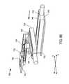
- FIG. 1illustrates a conventional X-Y translation stage that includes flexures for gripping a disk. Flexures are widely used in precision machines because they may provide frictionless, particle-free and low maintenance operation, while providing high precision. However, flexure based systems have limited ranges of motion and may not be adequate to center a disk relative to the imprinting surface of a stamper. The translation stage allows heat to dissipate from the surface of the disk that may result in inconsistent imprint patterns. Moreover, the use of such high precision actuators and robotics are expensive, with high maintenance costs, inconsistent accuracy and reliability, slow cycle times, and mechanical breakdown. The high precision actuators and robotics are bulky pieces of machinery, requiring large amounts of floor space.
- FIG. 1illustrates a conventional X-Y translation stage that includes flexures for gripping a substrate.
- FIG. 2illustrates one embodiment an imprinting system.
- FIG. 3illustrates an alternative embodiment of an imprinting system.
- FIG. 4illustrates another embodiment of an imprinting system.
- FIG. 4Aillustrates an enlarged view of a heater assembly that is part of the imprinting system of FIG. 4 .
- FIGS. 5A-5Bshow alternate views of a disk substrate transporting device that is part an imprinting system.
- FIG. 6illustrates one embodiment of a die assembly of an imprinting system.
- FIG. 7illustrates another embodiment of a die assembly of an imprinting system.
- FIG. 7Aillustrates a cross-sectional view of the die assembly shown in FIG. 7 .
- FIG. 7Billustrates an enlarged view of the cross-sectional view of the die assembly shown in FIG. 7A .
- FIG. 8illustrates an enlarged view of one embodiment of a disk transporting device.
- FIGS. 9A-9Cillustrate one embodiment of a disk transporting device in various positions.
- FIG. 10illustrates an enlarged view of a portion of a disk transporting device with a disk substrate clamped onto a support tray.
- FIG. 11illustrates an alternative embodiment of clamping or gripping structure that may be embedded within a support tray.
- FIG. 12illustrates one embodiment of a gripper embedded within a support tray for a clamping disk substrate.
- FIG. 13Ais a flow chart illustrating one embodiment of a method of imprinting an embossable film disposed above a disk substrate with an imprinting system.
- FIG. 13Bis a flow chart illustrating an alternative embodiment of a method of imprinting an embossable film disposed above a disk substrate with an imprinting system.
- FIG. 13Cis a flow chart illustrating an alternative embodiment of a method of imprinting an embossable film disposed above a disk substrate with an imprinting system.
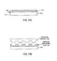
- FIG. 14Ais a cross sectional view illustrating one embodiment of an embossable film disposed above a disk substrate.
- FIG. 14Bis a cross sectional view illustrating one embodiment of the imprinting of an embossable film by an imprinting stamper.
- FIG. 15Ais a flow chart illustrating one embodiment of a method of imprinting an embossable film.
- FIG. 15Bis a flow chart illustrating an alternative embodiment of a method of imprinting an embossable film.
- FIG. 15Cis a flow chart illustrating another embodiment of a method of imprinting an embossable film.
- first layer or component disposed above or below another layer or componentmay be directly in contact with the first layer or component or may have one or more intervening layers or components.
- one layer or component disposed next to or adjacent another layer or componentmay be directly in contact with the first layer or component or may have one or more intervening layers or components.
- the apparatus and methods discussed hereinmay be used with various types of substrates (e.g., disk substrates and wafer substrates).
- the apparatus and methods discussed hereinmay be used for the imprinting of embossable materials for the production of magnetic recording disks.
- the magnetic recording diskmay be, for example, a DTR longitudinal magnetic recording disk having, for example, a nickel-phosphorous (NiP) plated substrate as a base structure.
- the magnetic recording diskmay be a DTR perpendicular magnetic recording disk having a soft magnetic film disposed above a substrate for the base structure.
- the apparatus and methods discussed hereinmay be used for the imprinting of embossable materials for the production of other types of digital recording disks, for examples, optical recording disks such as a compact disc (CD) and a digital-versatile-disk (DVD).
- optical recording diskssuch as a compact disc (CD) and a digital-versatile-disk (DVD).
- the apparatus and methods discussed hereinmay be used in other applications, for examples, the production of semiconductor wafers, display panels (e.g., liquid crystal display panels), etc.
- an imprint embossing systemis described with respect to a disk substrate.
- embodiments of an imprint embossing systemmay be easily adapted for substrates that vary in shape and size (e.g., square, rectangular), for the production of different types of substrates discussed above.
- Embodiments of an imprinting system described hereinmay be used for imprinting embossable films with nano-imprint lithography techniques. Alternatively, other scale imprint lithography techniques may be used, such as micro-imprint lithography.
- FIG. 2illustrates one embodiment of an imprinting system 200 that includes imprint or die assembly 210 , heater assembly 230 , heat tunnel 240 , disk substrate cooling station 250 , and disk cassette 260 mounted to table 201 .
- Assembly 200also includes a disk substrate transporting device 220 disposed next to table 201 .
- transporting device 220may be a vacuum chuck coupled to a robotic arm that extends over table 201 .
- Imprint assembly 210includes upper die assembly 212 and lower die assembly 214 that may include one or more embossing foils (a.k.a., stamper) that press into an embossable film disposed above a disk substrate to transfer a pattern into the embossable film.
- Heater 230 having heating element 232may be used to pre-heat the embossable film on the disk substrate to a desired embossing temperature.
- Heating element 232may also extend along a length of top and bottom portions 242 , 244 that form heat tunnel 240 .
- heater 230 and heating element 232may have separate heating sources.
- heater 230 and heating element 232may share the same heating source.
- heating element 232may be heat coils utilizing inductive heating to maintain the temperature of the embossable film.
- heat element 232may be another type of element, for example, an infrared (IR) heat source.
- a heat tunnelconnects heater 230 with die assembly 210 in order to maintain the desired embossing temperature during transport of the disk substrate from heater 230 to die assembly 210 .
- transporting device 220picks up a disk substrate from cassette 260 using vacuum chuck 224 .
- Vacuum chucks for handling disk substratesare known in the art; accordingly, a detailed description is not provided herein.
- other pick and place devices known in the artmay be used to remove a disk substrate from cassette 260 .
- a disk substratemay be pre-heated to bring up the temperature of the embossable film on the disk substrate to an optimum embossing level. To do so, in one embodiment, vacuum chuck 224 places a disk substrate within heater 230 .
- the embossable film on the disk substratemay be heated to a temperature in the range of approximately 20 to 350 degrees C.
- the vacuum chuck 224moves the disk substrate through heat tunnel 240 towards die assembly 210 .
- the disk substrateis then centered relative to the top and/or bottom embossing foils and then pressed against the embossable film of the disk substrate to form an embossing pattern (e.g., DTR pattern).
- an embossing patterne.g., DTR pattern
- heat tunnel 240minimizes thermal dissipation of the heated embossable film of the disk substrate. Thermal dissipation may lead to inconsistencies in the embossable film subsequent inconsistencies in the embossed pattern. As discussed above, heat tunnel 240 maintains the approximate embossing temperature of the heated embossable film until the disk substrate is placed in the die assembly. Although the embossing foils in die assembly 210 may be heated, a heated embossable film may result in a quicker and more efficient imprint. Moreover, by positioning heater assembly 280 relatively close to die assembly 210 , thermal distortion of the embossable film is minimized.
- FIG. 3illustrates another embodiment of an imprinting system 300 having a heater 330 disposed near die assembly 310 that does not include a heat tunnel as shown above with respect to FIG. 2 .
- the close proximity of heater 330 to die assembly 310may not require a heat tunnel to maintain the temperature of the embossable film/disk substrate that is sufficiently close to the desired embossing temperature.
- Vacuum chuck 324coupled to robotic arm 322 of transporting device 320 , moves a disk substrate around imprinting system 300 .
- a disk substratemay be transported from cassette 360 to heater 330 to be pre-heated to a temperature below, substantially at, or above the desired embossing temperature.
- the preheated embossable film/disk substrateis positioned in close proximity (e.g., nest area of lower die assembly 314 ) to the die assembly 310 .
- the embossable film/disk substratemay be preheated to a temperature below that of (e.g., close to) the embossing temperature and then heated to the embossing temperature during or after its positioning close to die assembly 310 .
- embossable film/disk substratemay be preheated to the die assembly's temperature/embossing temperature and imprinted after its close positioning to die assembly 310 .
- Die assembly 310may include one or more embossing foils for imprinting the embossable film disposed above a disk substrate transported from cassette 360 .
- An embossing foilis then pressed into the embossable film at the embossing temperature.
- the embossing foilis then separated from embossable film after imprinting. Then, the disk substrate may be transported to die assembly 310 to be embossed followed by a period at cooling station 350 .
- Heater 330 of FIG. 3is illustrated in a partially see-through view to show some of its internal components.
- a heat lamp 334is disposed near a top portion of heater 330 to serve as the heat source.
- An ejecting tray 332is disposed below heat lamp 334 to receive a disk substrate. Ejecting tray 332 slides out from heater 330 to receive a disk substrate from vacuum chuck 324 and slides back in under heat lamp 334 .
- Tray 332in one embodiment, may also have a spinning mechanism that spins a disk substrate while heating the embossable film.
- Cooling station 350includes a receiving tray 352 for a disk substrate to rest on after being imprinted in die assembly 310 .
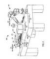
- FIG. 4illustrates an alternative embodiment of an imprinting system 400 that includes imprint or die assembly 410 , disk substrate transport device in the form of an infeed/outfeed assembly 420 , visual assembly 470 , and heater assembly 480 mounted to table 401 .
- Assembly 400also includes a robotic arm assembly 440 positioned next to table 401 .
- Imprint assembly 410includes upper die assembly 402 and lower die assembly 404 . The upper and lower die assemblies are disposed above press baseplate 406 .
- Draw bars 408 and 409couple the upper and lower die assemblies 402 , 404 and extend through table 401 .
- Imprint assembly 410also includes embossing die foils coupled to adjustable die holders (not shown). The die holders are fixed to a high precision, rolling element bushing die set.
- the die setis controlled by a stout framework, which accommodates a large diameter, low-pressure, high forced sealed bladder (not shown, but disposed below table 401 ).
- gase.g., air
- Cross beam 419moves a top plate of the die set down to compress the dies together.
- infeed/outfeed assembly 420may be a servo slide having a tray portion 430 that receives a disk substrate from robotic arm assembly 440 and slides the disk substrate through heater 480 and into die assembly 410 .
- robotic arm assembly 440transports a disk substrate from cassette 460 and places it on a disk holder plate 430 of infeed/outfeed assembly 420 .
- Robotic arm assembly 440includes link arm 442 coupled to one end of upper arm 444 to allow for full rotational movement around table 401 .
- Assembly 400has the ability to impart thermal qualities to the handling of disk substrates.
- the embossable film disposed above a disk substratemay be pre-heated to bring up the temperature of the embossable film on the disk substrate to an optimum embossing level.
- Disk holder plate 430may be positioned within heater assembly 480 to heat the embossable film to an optimum embossing temperature.
- the embossable film disposed above a disk substratemay be heated to a temperature in the range of approximately 20 to 350 degrees C.
- disk infeed/outfeed assembly 420continues to move the disk substrate between top die 402 and bottom die 404 of die assembly 410 .
- the disk substrateis then centered relative to the top and bottom embossing foils which are pressed into the embossable film to form an embossing pattern (e.g., DTR pattern).
- infeed/outfeed assembly 420may retract the disk substrate back into heater assembly 480 for inspection with visual assembly 470 .
- an inspection stepmay be used to ensure that the embossed pattern is centered on the disk substrate.
- the visual assembly 470inspects target track features on the imprinted embossable film to determine if its features are concentric with a center hole. This inspection routine may be done on a real-time or sampling basis.
- the use of heater assembly 480provides the advantage of pre-heating the embossable film disposed on the disk substrate to an embossing temperature. Although the embossing foils in die assembly 410 may be heated, a heated embossable film/disk substrate may result in quicker and more efficient imprint. Moreover, thermal distortion of the disk substrate is minimized by positioning heater assembly 480 relatively close to die assembly 410 .
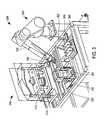
- FIG. 4Aillustrates an enlarged view of die assembly 410 , visual assembly 470 , and heater assembly 480 of assembly 400 .
- heater assembly 480includes a stand 486 that positions a heater box portion 481 at a height level with die assembly 410 and between top die 402 and bottom die 404 .
- Box portion 481includes an opening 484 to receive disk holder tray 430 , and well as an opening 482 near a top surface to allow a line of sight for microscope 472 of visual assembly 470 .
- opening 482may be covered with transparent glass.
- Bracket 474allows microscope 472 to be positioned above box portion 481 .
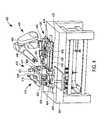
- FIGS. 5A and 5Billustrate an overall assembly of an embodiment for imprinting an embossable film disposed above a disk substrate.
- Assembly 500includes imprint assembly 510 , infeed/outfeed assembly 520 , robotic arm assembly 540 , and visual assembly 570 .
- Imprint assembly 510 and infeed/outfeed assembly 520 , and visual assembly 570are mounted to table 501 .
- Robotic arm assembly 540is positioned next to table 501 .
- robotic arm assembly 540takes a disk substrate to be imprinted from cassette 560 and transports it to the infeed/outfeed assembly 520 .
- Robotic arm assembly 540includes link arm 542 coupled to one end of upper arm 544 , and end effector 546 coupled to an opposite end of upper arm 544 . Palm extension 548 is coupled to end effector 546 , capable of holding a disk substrate on each side.
- Infeed/outfeed assembly 520includes a disk holder plate 530 supported on a pair of cantilevered flexures 526 , 528 , which in turn, are mounted on a precision X-Y servo slide (i.e., first slider 522 and second slider 524 ). In a retracted position the infeed/outfeed assembly 520 receives a disk substrate and securely maintains its position in a disk holder plate 530 .
- the disk substrateis clamped on his edges by 3 radially disposed fingers, which are linked together and supported by a series of flexure joints (discussed in greater detail below).
- a single thrusting actuatorrepeatedly captures a disk substrate in the exact same position.
- Cantilevered flexures 526 , 528allow disk holder plate 530 to be urged up or down within imprint assembly 510 .
- the infeed/outfeed assembly 520can be commanded to position a disk substrate at the center of the imprinting foil dies precisely. This positional information may be obtained by inspection feedback from the visual assembly 570 .
- Imprint assembly 510includes upper die assembly 502 and lower die assembly 504 .
- the upper and lower die assembliesare disposed above press baseplate 506 .
- Draw bars 508 and 509couple the upper and lower die assemblies 502 , 504 and extend through table 501 .
- Imprint assembly 510also includes embossing die foils coupled to adjustable die holders (not shown).
- the die holdersare fixed to a high precision, rolling element bushing die set.
- the die setis controlled by a stout framework, which accommodates a large diameter, low-pressure, high forced sealed bladder (not shown, but disposed below table 501 ). Upon application of gas pressure to the bladder, it expands against a thrust plate, which causes draw bars 508 , 509 to pull down on overhead yolk or cross beam 519 .
- Cross beam 519moves a top plate of the die set down to compress the dies together.
- the disk substratemay then be inspected by visual assembly 570 for proper alignment.
- the visual assembly 570inspects target track features on the embossable film to determine if track features are concentric with a center hole of the disk substrate.
- a computer/controller ormay command the final position of the servo slide to correspond with the exact center of the imprinting dies or foils when placing the disk substrate. This inspection routine may be done on a real-time or sampling basis.
- Infeed/outfeed assembly 520includes a first slider 522 , a second slider 524 disposed above and perpendicular to first slider 522 , flex supports 526 , 528 extending from second slider 524 , and holder plate 530 disposed near and end portion of flex supports 526 , 528 .
- first and second sliders 522 , 524form an X-Y servo slide mechanism.
- Holder plate 530is configured to receive a disk substrate (e.g., disk substrates 550 , 551 ).
- palm extension 548may hold to disk substrates at one time.
- Visual unit 570may be positioned between imprint assembly 510 and infeed/outfeed assembly 520 .
- Bracket 574is mounted to table 521 , with microscope 572 coupled to a top portion of bracket 574 .
- FIG. 5Aillustrates one end of palm extension 548 positioning disk substrate 551 in holder plate 530 .
- FIG. 5Billustrates holder plate 530 positioned between upper die assembly 502 and lower die assembly 504 of imprint assembly 510 .
- Second slider 524slides along rails on first slider 522 to advance holder plate 530 towards imprint assembly 510 .
- the palm extension 548returns to cassette 560 to retrieve additional disk substrates.
- robotic arm 540may also be used to retrieve a disk substrate after it has been imprinted with imprint assembly 510 .
- Visual assembly 570may be used to check for proper alignment of the imprinting foils on the disk substrate. The proper alignment for a disk substrate may be achieved by the X-Y servo mechanism of infeed/outfeed assembly 520 .
- a vision assemblyinspects a disk substrate after an embossing procedure to check for proper alignment with respect to a disk substrate center.
- the disk substrateis retracted from the imprint assembly and positioned to a known reference point directly below a microscope or an optical device (e.g., camera).
- the pattern printed on the diskis then examined. If it is found that the imprinted pattern is offset, instructions may be forwarded to the infeed/outfeed assembly to shift the holder plate to the proper position via the X-Y servo slide. This permits future disk substrates to be aligned properly with the embossing foils.
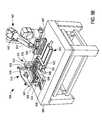
- FIG. 6illustrates one embodiment of a die assembly 600 .
- die assembly 600may be the same as the die assemblies discussed above with respect to FIGS. 2 , 3 , and 4 .
- An upper portion of imprint assembly 600includes top cross beam 620 , upper die assembly 602 , lower die assembly 604 , and press baseplate 606 .
- Upper die assembly 602 and lower die assembly 600are coupled by posts 610 , 611 , 612 , and 613 .
- the base portion of each posthas a bushing (e.g., bushings 614 , 615 , 616 , and 617 ).
- Upper die assembly 602also includes upper holder 640 for mounting an upper imprinting foil 650 .
- Lower die assembly 604includes lower holder 642 for mounting a lower imprinting foil (not shown).
- Lower holder 642is disposed above lower holder base 646 , floater plate 647 , and baseplate 648 .
- Upper and lower die assemblies 602 , 604are disposed above press base plate 606 .
- a lower portion of imprint assembly 600includes gas actuators 660 disposed between first bottom baseplate 607 and second bottom baseplate 667 .
- Lower cross beam 622is disposed below second bottom baseplate 667 .
- Spring rods 631 , 632 , 633 , and 634allow first bottom baseplate 607 and second bottom baseplate 667 to compress gas actuator 660 .
- second bottom baseplate 667moves downward and away from first bottom baseplate 607 , with springs 661 , 662 , 663 , and 664 .
- This expansioncauses top cross beam 620 to lower and force upper holder 640 and lower holder 642 together.
- the gap between press baseplate 606 and first bottom baseplate 607would be where the upper lower portions of input assembly 600 would be mounted, for example, to table as illustrated in FIG. 2A .
- FIG. 7illustrates one embodiment of an enlarged view of the top portion of imprint assembly 600 .
- Top support 603 of top die assembly 602is substantially similar in size and shape with lower support 605 of lower die assembly 604 .
- Posts 610 , 611 , 612 , and 613are disposed near the corners of the rectangular shaped top and lower supports.
- Each of the postshave a cylindrical shape having an outer diameter that is slightly less than an inner diameter of each of the bushings (e.g., 614 , 615 , 616 , and 617 ) to allow upper die assembly 602 to move down towards lower die assembly 604 .
- Upper holder 640is coupled near a central portion of top support 603 .
- lower holder 642is disposed above base 646 , float plate 647 , and baseplate 648 .
- a number of pressure nozzles(e.g., 670 , 671 ) secure float plate 647 to baseplate 648 .
- Screws mounted on each of the pressure nozzlesallow for adjustments of the flow plate 647 with respect to the baseplate 648 to align lower holder 642 with upper holder 640 properly. This may be necessary when adjustments are made to align lower embossing foil 651 with upper imprinting foil (not shown).
- imprint assembly 600allows for movement of top die assembly 602 towards lower die assembly 604 with the four posts mounted near the corners of top and lower supports.
- Lower holder 642may be moved or adjusted laterally to align itself with upper holder 640 properly.
- FIGS. 7A-7Billustrate cross-sectional views of one embodiment of upper die assembly 602 and lower die assembly 604 .
- a bottom embossing foil 651is disposed above a press pad 680 of lower die assembly 604 .
- press pad 680may include be one or more elastomeric layers 681 , 682 that allow for a uniform press of embossing foil 651 against the embossable film of disk substrate 650 .
- a central rod 684extends through a center portion of lower die assembly 604 and is coupled to spring 685 .
- Central rod 684has a tip portion 686 that is a tapered mandrel and exposed above press pad 680 and embossing foil 651 .
- Tip portion 686is tapered to fit inside the inner diameter (ID) of bottom foil 651 as well as disk substrate 650 .
- a linear ball bushing 688surrounds the elongated portion of central rod 684 , and an outer sleeve 690 surrounds linear ball bushing 618 .
- a ring portion 692is disposed between outer sleeve 690 and tapered portion 686 of central rod 684 . Ring portion 692 is also in contact with an ID of embossing foil 651 .
- a portion of the inner diameter of bottom foil 614extends downward and is disposed between lower mandrel 612 and outer sleeve 620 .
- linear ball bushing 688holds a precise alignment between central rod 684 and outer sleeve 690 to center embossing foil 651 with a centerline of central rod 684 .
- Ball bushing 688has a higher coefficient of thermal expansion compared to outer sleeve 620 . As such, when the temperature of lower die assembly 604 is raised, ball bushing 688 expands radially to hold a firm contact with outer sleeve 690 and to hold the centering alignment of bottom foil 651 with the inner diameter of outer sleeve 690 . This allows for a concentricity to be established and maintained between bottom foil 651 and disk substrate 650 .
- Ball bushing 688also maintains a contact with the inner diameter of bottom foil 651 through binding compressive force, which holds bottom foil 651 in place when disk substrate 650 is stripped off after imprinting.
- spring 685lifts outer sleeve 690 , which in turn lifts a portion of bottom foil 651 near the inner diameter. In effect, lifting outer sleeve 690 creates a dome-like shape for bottom foil 651 to strip disk substrate 650 cleanly off the surface of bottom foil 651 .
- FIG. 8illustrates an enlarged view of a disk transporting device in the form of infeed/outfeed assembly 700 without the slider portions.
- a holder plate 704is disposed on frame 702 .
- a disk substrate 750is secured to holder plate 704 with center finger 706 , first side finger 708 , and second side finger 710 radially disposed around disk substrate 750 .
- the fingersmay be linked together and supported by a series of flexure joints.
- Flexures 712 , 714allow holder plate 704 to move up and down when placed within the imprint assembly (e.g., imprint assemblies 410 , 510 described above with respect to FIGS. 4 , 4 A, 5 A, and 5 B).
- Holder plate 704may also be supported by fixed supports 716 , 718 . These supports are rigid to provide stiffness and support the weight of frame 702 .
- Top lifts 720 , 722couple fixed supports 716 , 718 to base plate 726 .
- One side of frame 702also includes a bracket 722 that has an opening to receive a thrusting actuator to rotate the flexure joints of center finger 706 , first side finger 708 , and second side finger 710 . As described in greater detail below, the thrusting actuator allows for a disk substrate to be captured repeatedly in the exact same position.
- FIGS. 9A-9Cillustrate infeed/outfeed assembly 700 in various slide positions including a load position as shown in FIG. 9A , an imprinting position as shown in FIG. 9B , and an inspection position as shown in FIG. 9C .
- holder plate 704is disposed on frame 702 .
- a pair of cantilevered flexures 712 , 714support holder plate 704 .
- a baseplate 726is mounted on an X-Y servo slide that includes first slider 740 and second slider 730 .
- Rails 732 , 734allow holder plate 704 to move along the Y-axis
- rails 742 , 744allow holder plate 704 to move along the X-axis.
- first and second sliders 730 , 740are part of a high precision X-Y servo slide. In the load position illustrated in FIG. 9A , second slider 730 is positioned near one end of first slider 740 to retract holder plate 704 . This position is similar to the position of infeed/outfeed assembly 520 illustrated in FIG. 5B , which allows a robotic arm assembly to place a disk substrate onto holder plate 704 . In the load position illustrated in FIG.
- second slider 730is positioned near an opposite end of first slider 740 to advance holder plate 704 into the imprint assembly. This position is similar to the position of infeed/outfeed assembly 520 illustrated in FIG. 5A , which shows the holder plate pressed between the upper and lower die assemblies.
- second slider 730is slightly retracted along the X-axis to position itself directly under a microscope of the vision assembly (e.g., microscope 572 of vision assembly 570 illustrated in FIG. 5A ).
- base plate 726may be moved along the rails 732 , 734 of second slider 730 (i.e., the Y-axis) to center the disk substrate with respect to the embossing foils of the imprinting assembly.
- FIG. 10illustrates an enlarged view of a portion of infeed/outfeed assembly 800 in one embodiment showing a disk substrate clamped onto a support plate.
- Holder plate 804is disposed on frame 802 .
- Flexures 812 , 814 and fixed supports 816 , 818are coupled to frame 802 .
- Central finger 806 , first side finger 808 , and second side finger 810are embedded within holder plate 804 .
- Each fingerhas extensions 830 , 832 , and 834 that make contact with and clamp disk substrate 850 .
- the fingersare linked together and supported by flexure joints 840 , 842 .
- a single thrusting actuatorcauses all the extensions (e.g., 830 , 832 , 834 ) to clamp disk substrate 850 at the same time and in the exact same position repeatedly.
- the thrusting actuatorenters through bracket 822 and applies force first towards central finger 806 . This in turn applies a force to first finger 808 and second finger 810 .
- a single thrusting actuatorprovides the advantage of being able to capture a disk in the exact same position each time.
- FIG. 11illustrates an alternative embodiment of clamping or gripping structure 900 that may be embedded within a plate holder.
- Gripper 900does not require a thrusting actuator but has an outer ring that includes a series of joints 920 , 922 , and 944 that connect fingers 912 , 914 , and 916 .
- Each of the fingershas extensions 912 , 914 , and 916 that are configured to make contact with an outer diameter of a disk substrate.
- Each of the jointsare flexible to allow the fingers to expand outward or pivot to receive a disk and then compress to make contact with the disk.
- FIG. 12illustrates one embodiment of gripper 900 embedded within holder plate 904 and clamping disk substrate 950 .
- Joints 920 , 922 , and 944have expanded outward to receive disk substrate 950 .
- Extensions 912 , 914 , and 916 of fingers 906 , 908 , and 910respectively make contact with an outer diameter 952 of disk substrate 950 .
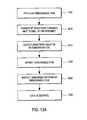
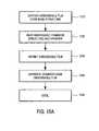
- FIGS. 13A , 13 B, and 13 Cillustrate embodiments of a method of imprinting an embossable film disposed above a substrate.
- An embossable film disposed above a substratee.g., a disk substrate
- the embossable substratemay be pre-heated in an oven (e.g., oven 330 ) designed to receive the substrate.
- the substrateis then transported through a heat tunnel (e.g., heat tunnel 240 ) to a die assembly, step 1010 .
- a heat tunnele.g., heat tunnel 240
- the substrateis centered or aligned relative to an embossing foil (e.g., embossing foil 651 ) disposed within the die assembly, step 1015 , followed by imprinting, step 1020 .
- the imprint pattern on the embossable film of the substratemay then be inspected, step 1025 , and then cooled, step 1030 .
- a substratee.g., a disk substrate
- a pick and place devicesuch as a vacuum chuck (e.g., 224 ) from a holding source, such as a cassette tray (e.g., 260 ), step 1040 .
- the vacuum chucktransports the substrate to a pre-heater (e.g., 230 ) to raise the temperature of the embossable film to an embossing temperature, step 1045 .
- the substrateis then removed from the heater and transported to a die assembly (e.g., 210 ), step 1050 , and centered relative to an embossing foil disposed within the die assembly, step 1055 .
- the embossable film of the substrateis imprinted with the pattern on the embossing foil, step 1060 and cooled, step 1065 .
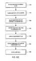
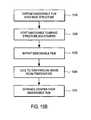
- a substratee.g., a disk substrate
- a servo slide traye.g., 430
- the servo slideis used to position the substrate in a heater (e.g., 480 ), and raise the temperature of the embossable film to an embossing temperature, step 1075 .
- the substrateis then removed from the heater and inserted into a die assembly (e.g., 410 ) for imprinting, step 1080 , and centered relative to an embossing foil, step 1085 .
- the embossable film of the substrateis then imprinted with the embossing pattern, step 1090 , followed by an inspection of the imprinted pattern, step 1095 .
- the substratemay then be cooled, step 1099 .
- the base structure 1110 of a diskmay be composed of a substrate 1115 and a plated NiP layer 1120 .
- Substrate 1115may be manufactured from, for examples, a glass or metal/metal alloy material.
- Glass substrates that may be usedinclude, for example, a silica containing glass such as borosilicate glass and aluminosilicate glass.
- Metal alloy substrates that may be usedinclude, for example, aluminum-magnesium (AlMg) substrates. In an alternative embodiment, other substrate materials including polymers and ceramics may be used.
- NiP layer 1120may be formed by electroplating, electroless plating, or by other methods known in the art.
- Plating disk substrate 1115 with a rigid or metallic material such as NiPprovides mechanical support to disk substrate 1115 for e.g., subsequent polishing, and/or imprinting processes.
- NiP layer 1120may be polished, planarized, and/or textured.
- NiP layer 1120may be polished, for example, by a uniform etch or other polishing techniques known in the art.
- NiP layer 1120may also be textured with a pattern, by various methods such as mechanical texturing using fixed or free abrasive particles (e.g., diamond). Alternatively, other types of texturing methods, such as laser texturing, may be used.
- Plating of disk substrate 1115may not be necessary, however, if disk substrate 1115 is composed of a sufficiently rigid or hard material such as glass. Accordingly, substrate 1115 , itself, may be polished, planarized, and/or textured using methods described above.
- base structure 1110may be composed of a substrate 1115 having other layers disposed thereon, for examples, a soft magnetic film.
- Layer 1120may represent a soft magnetic film or a soft magnetic film disposed over a NiP layer.
- a soft magnetic filmmay be used to achieve the proper magnetic properties associated with perpendicular magnetic recording.
- the soft magnetic filmmay be a layer of iron-copper-nickel (FeCoNi) material.
- Other materials that may be used for the soft magnetic filminclude copper-iron (CoFe) nickel-iron (NiFe), and alloys thereof.
- Soft magnetic films and materials that may be used for manufacturing a soft magnetic filmare well known in the art of magnetic recording disks; accordingly, a detailed discussion is not provided.
- the soft magnetic filmmay be polished and/or textured.
- the soft magnetic filmmay be textured with a pattern, by various methods such as mechanical texturing using fixed or free abrasive particles (e.g., diamond). Alternatively, other types of texturing methods, such as laser texturing, may be used to texture the soft magnetic film.
- a thin NiP layermay be disposed on top of the soft magnetic film and polished and/or textured.
- the soft magnetic filmmay be composed of one or more soft magnetic underlayers and one or more Ru interlayers disposed between soft magnetic underlayers.
- Embossable film 1130is disposed on the base structure 1110 in order to form an imprintable (i.e., embossable) film.
- Various embossable materialsmay be used to form the embossable film 1130 .
- PMMApoly(methyl methacrylate)
- P(MMA-MAA)co-polymer-poly(methyl methacrylate methacrylic acid copolymer)
- PMMA-MAAco-polymer-poly(methyl methacrylate methacrylic acid copolymer
- other embossable materialsmay be used for example, PMMA and a thermo-set polymer such as MR-I 9000 available from Micro Resists Technology of Germany.
- embossable film 1130may be composed of multiple embossable films.
- the embossable materialsmay be spin coated on base structure 1110 to produce the embossable film 1130 .
- Other coating methodssuch as dip coating, dip-spin coating, spray coating, sputtering and vacuum deposition (e.g., CVD) may be used.
- FIGS. 14A , 14 B, 15 A, 15 B and 15 Cillustrate alternative embodiments of a method of imprinting an embossable film such as an embossable film disposed above a base structure.
- the base structuremay be a substrate or a disk substrate.
- Embossable film 1130is disposed over base structure 1115 , step 1210 .
- embossable film 1130 /base structure 1115 and stamper 1190are heated at or above the “glass transition temperature” (Tg) of embossable film 1130 , step 1230 .
- the glass transition temperatureis a term of art that refers to the temperature where a polymer material becomes viscoelastic above this temperature (which is different for each polymer).
- Stamper 1190is then pressed into the embossable film 1130 , step 1235 .
- stamper 1190is separated from embossable film 1130 , step 1240 , and then cooled after separation, step 1243 .
- An imprinted pattern of trenches areas (a.k.a., recessed areas, grooves, valleys, etc.) and plateaus (a.k.a., raised areas)is thereby formed in the embossable film 1130 (as illustrated in FIG. 14B ).
- the separation of stamper 1190 from embossable film 1130 before coolingmay facilitate the separation process and result in less damage to the imprinted pattern in embossable film 1130 .
- the systemmay be cooled to a temperature above room temperature, step 1260 , prior to the separation of stamper 1190 from embossable film 1130 , step 1270 .
- the coupled stamper 1190 /embossable film 1130may be cooled to a lower temperature down to approximately the glass transition temperature of the embossable film 1130 prior to separation.
- the coupled stamper 1190 /embossable film 1130may be cooled to a temperature in the range of approximately at the transition temperature of the embossable film 1130 to just above room temperature.
- the coupled stamper 1190 /embossable film 1130may be cooled to room temperature and then separated.
- FIG. 15Cillustrates an alternative embodiment of imprinting an embossable film including preheating the embossable film prior to imprinting.
- embossable film 1130 and stamper 1190may be separately heated.
- this structuremay be preheated to the embossing temperature prior its introduction into die assembly 230 by, for example, heater 230 of FIG. 2 .
- the preheated embossable film 1130 /base structure 1115is positioned in close proximity (e.g., nest area of lower die assembly 214 ) to the stamper 1190 .
- the embossable film 1130 /base structure 1115may be preheated to a temperature below that of (e.g., close to) the embossing temperature and then heated to the embossing temperature during or after its positioning in the nest area of lower die assembly 214 .
- the embossable film 1130 /base structure 1115may be preheated to the stamper's temperature/embossing temperature and imprinted after its close positioning to stamper 1190 .
- Stamper 1190is then pressed into the embossable film 1130 at the embossing temperature, step 1230 .
- the stamper 1190is then separated from embossable film 1130 after imprinting, step 1240 .
- the embossable film 1130 /base structure 1115may be removed from close proximity to stamper 1190 , step 1241 , and then cooled to a temperature below the glass transition temperature of embossable film 1130 .
- the stamper 1190is then separated from embossable film 1130 after imprinting.
- the embossable film 1130 /base structure 1115may be removed from close proximity to stamper 1190 and then cooled to a temperature below the glass transition temperature of embossable film 1130 , step 1243 .
- An imprinted pattern of trenches areas(a.k.a., recessed areas, grooves, valleys, etc.) and plateaus (a.k.a., raised areas) is thereby formed in the embossable film 1230 (as illustrated in FIG. 14B ).
- a subtractive or an additive processmay be used to form the desired DTR pattern in the disk.
- one or more layers disposed above the substrate 1115may be removed (e.g., through imprint lithography and etching) to expose a desired pattern on layer 1120 (e.g., a NiP or soft magnetic layer).
- the DTR patternmay be formed in substrate 1115 .
- layer 1120is, for example, a NiP layer
- a material compatible or identical to material forming the initial NiP layeris added or plated to form the raised areas 1110 of the discrete track recording pattern.
- the imprinting of an embossable film 1130may be performed at approximately room temperature using an embossable material that does not have a glass transition temperature (Tg), for examples, thermosetting (e.g., epoxies, phenolics, polysiloxanes, ormosils, silica-gel) and radiation curable (e.g., UV curable, electron-beam curable) polymers.
- Tgglass transition temperature
- thermosettinge.g., epoxies, phenolics, polysiloxanes, ormosils, silica-gel
- radiation curablee.g., UV curable, electron-beam curable
- Silica-gelmay be obtained from industry manufacturers, for example, SOL-GEL available from General Electric Corp., of Waterford N.Y.
- a thermo plastic materialfor example, a polymer such as Ultem available from General Electric Corp., of Waterford N.Y. may be used for the embossable film.
- the apparatus and methods discussed hereinmay be used with various types of base structures (e.g., optical disk substrates and wafer substrates, panel substrates) having embossable films.
- the imprinting system discussed hereinmay be used in the production of optical recording disks, semiconductor wafers, liquid crystal display panels, etc.
- the apparatus and methods discussed hereinmay be used with various types of base structures (e.g., wafer and panel oxide/substrates) having an embossable layer disposed thereon.
- the imprinting apparatus and methods discussed hereinmay be used to fabricate semiconductor devices such as, for example, a transistor.
- an embossable layermay be disposed above a base structure of, for example, an oxide (e.g., SiO 2 ) layer on top of a silicon wafer substrate.
- a stampermay be generated with a patterned structure for active areas of the transistor. The stamper is imprinted into the embossable layer with the embossed pattern transferred into the oxide layer using etching techniques (e.g., reactive ion etching). Subsequent semiconductor wafer fabrication techniques well known in the art are used to produce the transistor.
- the imprinting apparatus and methods discussed hereinmay be used to fabricate pixel arrays for flat panel displays.
- an embossable layermay be disposed above a base structure of, for example, an indium tin oxide (ITO) layer on top of a substrate.
- ITOindium tin oxide
- the stamperis generated with a patterned layer being an inverse of the pixel array pattern.
- the stamperis imprinted into the embossable layer with the embossed pattern transferred into the ITO using etching techniques to pattern the ITO layer.
- each pixel of the arrayis separated by an absence of ITO material (removed by the etching) on the otherwise continuous ITO anode.
- Subsequent fabrication techniques well known in the artare used to produce the pixel array.
- the imprinting apparatus and methods discussed hereinmay be used to fabricate lasers.
- embossable material areas patterned by the stamperare used as a mask to define laser cavities for light emitting materials.
- Subsequent fabrication techniques well known in the artare used to produce the laser.
- the apparatus and methods discussed hereinmay be used in other applications, for example, the production of multiple layer electronic packaging, the production of optical communication devices, and contact/transfer printing.
Landscapes
- Engineering & Computer Science (AREA)
- Manufacturing & Machinery (AREA)
- Manufacturing Of Magnetic Record Carriers (AREA)
- Shaping Of Tube Ends By Bending Or Straightening (AREA)
- Moulds For Moulding Plastics Or The Like (AREA)
Abstract
Description
Claims (4)
Priority Applications (1)
| Application Number | Priority Date | Filing Date | Title |
|---|---|---|---|
| US12/555,780US8100685B1 (en) | 2004-01-20 | 2009-09-08 | Imprint embossing alignment system |
Applications Claiming Priority (2)
| Application Number | Priority Date | Filing Date | Title |
|---|---|---|---|
| US10/761,464US7686606B2 (en) | 2004-01-20 | 2004-01-20 | Imprint embossing alignment system |
| US12/555,780US8100685B1 (en) | 2004-01-20 | 2009-09-08 | Imprint embossing alignment system |
Related Parent Applications (1)
| Application Number | Title | Priority Date | Filing Date |
|---|---|---|---|
| US10/761,464ContinuationUS7686606B2 (en) | 2004-01-20 | 2004-01-20 | Imprint embossing alignment system |
Publications (1)
| Publication Number | Publication Date |
|---|---|
| US8100685B1true US8100685B1 (en) | 2012-01-24 |
Family
ID=34750173
Family Applications (2)
| Application Number | Title | Priority Date | Filing Date |
|---|---|---|---|
| US10/761,464Expired - Fee RelatedUS7686606B2 (en) | 2004-01-20 | 2004-01-20 | Imprint embossing alignment system |
| US12/555,780Expired - Fee RelatedUS8100685B1 (en) | 2004-01-20 | 2009-09-08 | Imprint embossing alignment system |
Family Applications Before (1)
| Application Number | Title | Priority Date | Filing Date |
|---|---|---|---|
| US10/761,464Expired - Fee RelatedUS7686606B2 (en) | 2004-01-20 | 2004-01-20 | Imprint embossing alignment system |
Country Status (4)
| Country | Link |
|---|---|
| US (2) | US7686606B2 (en) |
| JP (1) | JP4814527B2 (en) |
| DE (1) | DE102005001476A1 (en) |
| MY (1) | MY142294A (en) |
Cited By (70)
| Publication number | Priority date | Publication date | Assignee | Title |
|---|---|---|---|---|
| US20090263531A1 (en)* | 2008-04-17 | 2009-10-22 | Vijay Shilpiekandula | Symmetric thermocentric flexure with minimal yaw error motion |
| US20110026162A1 (en)* | 2008-03-30 | 2011-02-03 | Hoya Corporation | Magnetic disk and method of manufacturing the same |
| US8402638B1 (en) | 2009-11-06 | 2013-03-26 | Wd Media, Inc. | Press system with embossing foil free to expand for nano-imprinting of recording media |
| US8496466B1 (en) | 2009-11-06 | 2013-07-30 | WD Media, LLC | Press system with interleaved embossing foil holders for nano-imprinting of recording media |
| US8828566B2 (en) | 2010-05-21 | 2014-09-09 | Wd Media (Singapore) Pte. Ltd. | Perpendicular magnetic recording disc |
| US8859118B2 (en) | 2010-01-08 | 2014-10-14 | Wd Media (Singapore) Pte. Ltd. | Perpendicular magnetic recording medium |
| US8867322B1 (en) | 2013-05-07 | 2014-10-21 | WD Media, LLC | Systems and methods for providing thermal barrier bilayers for heat assisted magnetic recording media |
| US8877359B2 (en) | 2008-12-05 | 2014-11-04 | Wd Media (Singapore) Pte. Ltd. | Magnetic disk and method for manufacturing same |
| US8908315B2 (en) | 2010-03-29 | 2014-12-09 | Wd Media (Singapore) Pte. Ltd. | Evaluation method of magnetic disk, manufacturing method of magnetic disk, and magnetic disk |
| US8941950B2 (en) | 2012-05-23 | 2015-01-27 | WD Media, LLC | Underlayers for heat assisted magnetic recording (HAMR) media |
| US8947987B1 (en) | 2013-05-03 | 2015-02-03 | WD Media, LLC | Systems and methods for providing capping layers for heat assisted magnetic recording media |
| US8951651B2 (en) | 2010-05-28 | 2015-02-10 | Wd Media (Singapore) Pte. Ltd. | Perpendicular magnetic recording disk |
| US8980076B1 (en) | 2009-05-26 | 2015-03-17 | WD Media, LLC | Electro-deposited passivation coatings for patterned media |
| US8993134B2 (en) | 2012-06-29 | 2015-03-31 | Western Digital Technologies, Inc. | Electrically conductive underlayer to grow FePt granular media with (001) texture on glass substrates |
| US8995078B1 (en) | 2014-09-25 | 2015-03-31 | WD Media, LLC | Method of testing a head for contamination |
| US9001630B1 (en) | 2011-03-08 | 2015-04-07 | Western Digital Technologies, Inc. | Energy assisted magnetic recording medium capable of suppressing high DC readback noise |
| US9025264B1 (en) | 2011-03-10 | 2015-05-05 | WD Media, LLC | Methods for measuring media performance associated with adjacent track interference |
| US9029308B1 (en) | 2012-03-28 | 2015-05-12 | WD Media, LLC | Low foam media cleaning detergent |
| US9028985B2 (en) | 2011-03-31 | 2015-05-12 | WD Media, LLC | Recording media with multiple exchange coupled magnetic layers |
| US9034492B1 (en) | 2013-01-11 | 2015-05-19 | WD Media, LLC | Systems and methods for controlling damping of magnetic media for heat assisted magnetic recording |
| US9042053B1 (en) | 2014-06-24 | 2015-05-26 | WD Media, LLC | Thermally stabilized perpendicular magnetic recording medium |
| US9047880B1 (en) | 2011-12-20 | 2015-06-02 | WD Media, LLC | Heat assisted magnetic recording method for media having moment keeper layer |
| US9047903B2 (en) | 2008-03-26 | 2015-06-02 | Wd Media (Singapore) Pte. Ltd. | Perpendicular magnetic recording medium and process for manufacture thereof |
| US9064521B1 (en) | 2011-03-25 | 2015-06-23 | WD Media, LLC | Manufacturing of hard masks for patterning magnetic media |
| US9082447B1 (en) | 2014-09-22 | 2015-07-14 | WD Media, LLC | Determining storage media substrate material type |
| US9093122B1 (en) | 2013-04-05 | 2015-07-28 | WD Media, LLC | Systems and methods for improving accuracy of test measurements involving aggressor tracks written to disks of hard disk drives |
| US9093100B2 (en) | 2008-03-17 | 2015-07-28 | Wd Media (Singapore) Pte. Ltd. | Magnetic recording medium including tailored exchange coupling layer and manufacturing method of the same |
| US9142241B2 (en) | 2009-03-30 | 2015-09-22 | Wd Media (Singapore) Pte. Ltd. | Perpendicular magnetic recording medium and method of manufacturing the same |
| US9153268B1 (en) | 2013-02-19 | 2015-10-06 | WD Media, LLC | Lubricants comprising fluorinated graphene nanoribbons for magnetic recording media structure |
| US9159350B1 (en) | 2014-07-02 | 2015-10-13 | WD Media, LLC | High damping cap layer for magnetic recording media |
| US9177586B2 (en) | 2008-09-30 | 2015-11-03 | WD Media (Singapore), LLC | Magnetic disk and manufacturing method thereof |
| US9177585B1 (en) | 2013-10-23 | 2015-11-03 | WD Media, LLC | Magnetic media capable of improving magnetic properties and thermal management for heat-assisted magnetic recording |
| US9183867B1 (en) | 2013-02-21 | 2015-11-10 | WD Media, LLC | Systems and methods for forming implanted capping layers in magnetic media for magnetic recording |
| US9190094B2 (en) | 2013-04-04 | 2015-11-17 | Western Digital (Fremont) | Perpendicular recording media with grain isolation initiation layer and exchange breaking layer for signal-to-noise ratio enhancement |
| US9196283B1 (en) | 2013-03-13 | 2015-11-24 | Western Digital (Fremont), Llc | Method for providing a magnetic recording transducer using a chemical buffer |
| US9218850B1 (en) | 2014-12-23 | 2015-12-22 | WD Media, LLC | Exchange break layer for heat-assisted magnetic recording media |
| US9227324B1 (en) | 2014-09-25 | 2016-01-05 | WD Media, LLC | Mandrel for substrate transport system with notch |
| US9240204B2 (en) | 2010-05-21 | 2016-01-19 | Wd Media (Singapore) Pte. Ltd. | Perpendicular magnetic recording disc |
| US9257134B1 (en) | 2014-12-24 | 2016-02-09 | Western Digital Technologies, Inc. | Allowing fast data zone switches on data storage devices |
| US9269480B1 (en) | 2012-03-30 | 2016-02-23 | WD Media, LLC | Systems and methods for forming magnetic recording media with improved grain columnar growth for energy assisted magnetic recording |
| US9275669B1 (en) | 2015-03-31 | 2016-03-01 | WD Media, LLC | TbFeCo in PMR media for SNR improvement |
| US9280998B1 (en) | 2015-03-30 | 2016-03-08 | WD Media, LLC | Acidic post-sputter wash for magnetic recording media |
| US9296082B1 (en) | 2013-06-11 | 2016-03-29 | WD Media, LLC | Disk buffing apparatus with abrasive tape loading pad having a vibration absorbing layer |
| US9330685B1 (en) | 2009-11-06 | 2016-05-03 | WD Media, LLC | Press system for nano-imprinting of recording media with a two step pressing method |
| US9349404B2 (en) | 2010-05-28 | 2016-05-24 | Wd Media (Singapore) Pte. Ltd | Perpendicular magnetic recording disc |
| US9382496B1 (en) | 2013-12-19 | 2016-07-05 | Western Digital Technologies, Inc. | Lubricants with high thermal stability for heat-assisted magnetic recording |
| US9389135B2 (en) | 2013-09-26 | 2016-07-12 | WD Media, LLC | Systems and methods for calibrating a load cell of a disk burnishing machine |
| US9401300B1 (en) | 2014-12-18 | 2016-07-26 | WD Media, LLC | Media substrate gripper including a plurality of snap-fit fingers |
| US9406330B1 (en) | 2013-06-19 | 2016-08-02 | WD Media, LLC | Method for HDD disk defect source detection |
| US9406329B1 (en) | 2015-11-30 | 2016-08-02 | WD Media, LLC | HAMR media structure with intermediate layer underlying a magnetic recording layer having multiple sublayers |
| US9431045B1 (en) | 2014-04-25 | 2016-08-30 | WD Media, LLC | Magnetic seed layer used with an unbalanced soft underlayer |
| US9449633B1 (en) | 2014-11-06 | 2016-09-20 | WD Media, LLC | Smooth structures for heat-assisted magnetic recording media |
| US9447368B1 (en) | 2014-02-18 | 2016-09-20 | WD Media, LLC | Detergent composition with low foam and high nickel solubility |
| US9472227B2 (en) | 2010-06-22 | 2016-10-18 | Wd Media (Singapore) Pte. Ltd. | Perpendicular magnetic recording media and methods for producing the same |
| US9542968B1 (en) | 2010-08-20 | 2017-01-10 | WD Media, LLC | Single layer small grain size FePT:C film for heat assisted magnetic recording media |
| US9558778B2 (en) | 2009-03-28 | 2017-01-31 | Wd Media (Singapore) Pte. Ltd. | Lubricant compound for magnetic disk and magnetic disk |
| US9581510B1 (en) | 2013-12-16 | 2017-02-28 | Western Digital Technologies, Inc. | Sputter chamber pressure gauge with vibration absorber |
| US9607646B2 (en) | 2013-07-30 | 2017-03-28 | WD Media, LLC | Hard disk double lubrication layer |
| US9685184B1 (en) | 2014-09-25 | 2017-06-20 | WD Media, LLC | NiFeX-based seed layer for magnetic recording media |
| US9818442B2 (en) | 2014-12-01 | 2017-11-14 | WD Media, LLC | Magnetic media having improved magnetic grain size distribution and intergranular segregation |
| US9824711B1 (en) | 2014-02-14 | 2017-11-21 | WD Media, LLC | Soft underlayer for heat assisted magnetic recording media |
| US9822441B2 (en) | 2015-03-31 | 2017-11-21 | WD Media, LLC | Iridium underlayer for heat assisted magnetic recording media |
| US9990940B1 (en) | 2014-12-30 | 2018-06-05 | WD Media, LLC | Seed structure for perpendicular magnetic recording media |
| US10054363B2 (en) | 2014-08-15 | 2018-08-21 | WD Media, LLC | Method and apparatus for cryogenic dynamic cooling |
| US10083715B2 (en) | 2010-05-28 | 2018-09-25 | WD Media (Singapore) Pte.Ltd. | Method of manufacturing a perpendicular magnetic disc |
| US10115428B1 (en) | 2013-02-15 | 2018-10-30 | Wd Media, Inc. | HAMR media structure having an anisotropic thermal barrier layer |
| US10121506B1 (en) | 2015-12-29 | 2018-11-06 | WD Media, LLC | Magnetic-recording medium including a carbon overcoat implanted with nitrogen and hydrogen |
| US10236026B1 (en) | 2015-11-06 | 2019-03-19 | WD Media, LLC | Thermal barrier layers and seed layers for control of thermal and structural properties of HAMR media |
| CN110142704A (en)* | 2019-04-24 | 2019-08-20 | 贵州永红航空机械有限责任公司 | Aluminum plate fin type radiator Welding Testing fixture and method |
| US11074934B1 (en) | 2015-09-25 | 2021-07-27 | Western Digital Technologies, Inc. | Heat assisted magnetic recording (HAMR) media with Curie temperature reduction layer |
Families Citing this family (18)
| Publication number | Priority date | Publication date | Assignee | Title |
|---|---|---|---|---|
| US7686606B2 (en) | 2004-01-20 | 2010-03-30 | Wd Media, Inc. | Imprint embossing alignment system |
| US7684152B2 (en)* | 2004-09-24 | 2010-03-23 | Wd Media, Inc. | Method of mitigating eccentricity in a disk drive with DTR media |
| US7331283B2 (en)* | 2004-12-16 | 2008-02-19 | Asml Holding N.V. | Method and apparatus for imprint pattern replication |
| US7399422B2 (en)* | 2005-11-29 | 2008-07-15 | Asml Holding N.V. | System and method for forming nanodisks used in imprint lithography and nanodisk and memory disk formed thereby |
| US7409759B2 (en)* | 2004-12-16 | 2008-08-12 | Asml Holding N.V. | Method for making a computer hard drive platen using a nano-plate |
| US7410591B2 (en)* | 2004-12-16 | 2008-08-12 | Asml Holding N.V. | Method and system for making a nano-plate for imprint lithography |
| US7363854B2 (en)* | 2004-12-16 | 2008-04-29 | Asml Holding N.V. | System and method for patterning both sides of a substrate utilizing imprint lithography |
| EP1924425B1 (en)* | 2005-08-26 | 2012-07-04 | Quickstep Technologies Pty, Ltd | Reticulation system for composite component production |
| JP4738136B2 (en)* | 2005-10-31 | 2011-08-03 | 株式会社東芝 | Plate-like structure manufacturing apparatus and magnetic disk manufacturing method |
| JP5114848B2 (en)* | 2006-02-09 | 2013-01-09 | 凸版印刷株式会社 | Method for correcting defects in imprint mold and method for producing imprint mold |
| KR101261606B1 (en) | 2006-05-09 | 2013-05-09 | 삼성디스플레이 주식회사 | Apparatus for manufacturing a display panel and method for manufacturing the same |
| AR061903A1 (en)* | 2007-07-17 | 2008-10-01 | Eduardo Jose Collazuol | FAST CHANGE SYSTEM OF PNEUMATIC PUMP EXPULSION DEVICES FOR SOAP MATRIX |
| JP5370806B2 (en)* | 2008-04-22 | 2013-12-18 | 富士電機株式会社 | Imprint method and apparatus |
| JP5077764B2 (en)* | 2008-04-22 | 2012-11-21 | 富士電機株式会社 | Imprint method and apparatus |
| US7924519B2 (en)* | 2008-09-29 | 2011-04-12 | Wd Media, Inc. | Eccentricity determination for a disk |
| JP5218909B2 (en)* | 2008-12-22 | 2013-06-26 | 富士電機株式会社 | Imprint device |
| US20140264998A1 (en) | 2013-03-14 | 2014-09-18 | Q1 Nanosystems Corporation | Methods for manufacturing three-dimensional metamaterial devices with photovoltaic bristles |
| US9954126B2 (en) | 2013-03-14 | 2018-04-24 | Q1 Nanosystems Corporation | Three-dimensional photovoltaic devices including cavity-containing cores and methods of manufacture |
Citations (97)
| Publication number | Priority date | Publication date | Assignee | Title |
|---|---|---|---|---|
| US3946634A (en) | 1972-04-03 | 1976-03-30 | Letson And Burpee Ltd. | Band mill strain mechanism |
| US4062600A (en) | 1976-04-05 | 1977-12-13 | Litton Systems, Inc. | Dual-gimbal gyroscope flexure suspension |
| US4343025A (en) | 1979-10-05 | 1982-08-03 | Nortronics Company, Inc. | Transducer arm assembly for floppy disk |
| US4571320A (en) | 1984-10-31 | 1986-02-18 | General Motors Corporation | Method and apparatus for loading and unloading sheet molding compound in and from a press |
| US4694703A (en) | 1984-06-28 | 1987-09-22 | Lear Siegler, Inc. | Circumferentially oriented flexure suspension |
| US4770739A (en) | 1987-02-03 | 1988-09-13 | Texas Instruments Incorporated | Bilayer photoresist process |
| US4778372A (en) | 1983-10-06 | 1988-10-18 | Servichem Ag | Thermoplastic web conveying mechanism and thermoforming apparatus |
| US4786564A (en) | 1987-02-25 | 1988-11-22 | Komag, Inc. | Method for manufacturing a magnetic disk having reduced bit shift, minimized noise, increased resolution and uniform magnetic characteristics, and the resulting disk |
| US4931351A (en) | 1987-01-12 | 1990-06-05 | Eastman Kodak Company | Bilayer lithographic process |
| US5018037A (en) | 1989-10-10 | 1991-05-21 | Krounbi Mohamad T | Magnetoresistive read transducer having hard magnetic bias |
| US5045150A (en) | 1986-09-11 | 1991-09-03 | National Semiconductor Corp. | Plasma etching using a bilayer mask |
| US5045165A (en) | 1990-02-01 | 1991-09-03 | Komag, Inc. | Method for sputtering a hydrogen-doped carbon protective film on a magnetic disk |
| US5077888A (en) | 1989-02-17 | 1992-01-07 | Hitachi, Ltd. | Article assembling method and device |
| US5080549A (en) | 1987-05-11 | 1992-01-14 | Epsilon Technology, Inc. | Wafer handling system with Bernoulli pick-up |
| US5091047A (en) | 1986-09-11 | 1992-02-25 | National Semiconductor Corp. | Plasma etching using a bilayer mask |
| US5219788A (en) | 1991-02-25 | 1993-06-15 | Ibm Corporation | Bilayer metallization cap for photolithography |
| US5259926A (en) | 1991-09-24 | 1993-11-09 | Hitachi, Ltd. | Method of manufacturing a thin-film pattern on a substrate |
| US5290397A (en) | 1992-08-21 | 1994-03-01 | Cornell Research Foundation, Inc. | Bilayer resist and process for preparing same |
| US5293287A (en) | 1990-05-18 | 1994-03-08 | Iomega Corporation | Apparatus and methods for backside stabilization of flexible optical media in information storage system |
| US5295802A (en) | 1990-06-01 | 1994-03-22 | Richard Hersbt | Demolding apparatus |
| US5320934A (en) | 1991-06-28 | 1994-06-14 | Misium George R | Bilayer photolithographic process |
| US5322987A (en) | 1992-06-10 | 1994-06-21 | Iomega Corporation | Pneumatic hub locking device for etching optical servo tracks on magnetic disks |
| US5413018A (en) | 1991-06-20 | 1995-05-09 | Fuji Electric Co., Ltd. | Piezo-electric actuator operated press |
| US5427599A (en) | 1987-06-09 | 1995-06-27 | International Business Machines Corporation | System for stamping an optical storage disk |
| US5455145A (en) | 1988-12-24 | 1995-10-03 | Mitsubishi Denki Kabushiki Kaisha | Method of manufacturing double layer resist pattern and double layer resist structure |
| US5493959A (en) | 1993-08-23 | 1996-02-27 | Aida Engineering, Ltd. | Apparatus for correcting slide bottom dead center position of mechanical press |
| US5512131A (en) | 1993-10-04 | 1996-04-30 | President And Fellows Of Harvard College | Formation of microstamped patterns on surfaces and derivative articles |
| US5537282A (en) | 1994-07-15 | 1996-07-16 | Treves; David | Data storage disk having improved tracking capability |
| US5571473A (en) | 1989-12-28 | 1996-11-05 | Idemitsu Petrochemical Co., Ltd. | Process for thermoforming thermoplastic resin sheet |
| US5681638A (en) | 1994-04-27 | 1997-10-28 | Canon Kabushiki Kaisha | Substrate, and method and apparatus for holding the substrate |
| US5738008A (en) | 1995-08-31 | 1998-04-14 | Eastman Kodak Company | Clamping apparatus for disk-shaped information medium |
| US5772905A (en) | 1995-11-15 | 1998-06-30 | Regents Of The University Of Minnesota | Nanoimprint lithography |
| US5820769A (en) | 1995-05-24 | 1998-10-13 | Regents Of The University Of Minnesota | Method for making magnetic storage having discrete elements with quantized magnetic moments |
| US5888433A (en) | 1996-07-31 | 1999-03-30 | Kitano Engineering Co., Ltd. | Method of correcting nonalignment of a storage disc |
| US5894056A (en) | 1995-12-19 | 1999-04-13 | Nikon Corporation | Mask substrate, projection exposure apparatus equipped with the mask substrate, and a pattern formation method utilizing the projection exposure apparatus |
| US5915915A (en) | 1996-03-07 | 1999-06-29 | Komag, Incorporated | End effector and method for loading and unloading disks at a processing station |
| US5985524A (en) | 1997-03-28 | 1999-11-16 | International Business Machines Incorporated | Process for using bilayer photoresist |
| US6019930A (en) | 1992-07-14 | 2000-02-01 | Thermal Wave Molding Corp. | Process for forming a molten material into molded article |
| US6086730A (en) | 1999-04-22 | 2000-07-11 | Komag, Incorporated | Method of sputtering a carbon protective film on a magnetic disk with high sp3 content |
| US6150015A (en) | 1997-12-04 | 2000-11-21 | Komag, Incorporated | Ultra-thin nucleation layer for magnetic thin film media and the method for manufacturing the same |
| US6210855B1 (en) | 1996-09-19 | 2001-04-03 | Shin Etsu Chemical Co., Ltd. | Positive resist composition suitable for lift-off technique and pattern forming method |
| US6218056B1 (en) | 1999-03-30 | 2001-04-17 | International Business Machines Corporation | Method of making highly defined bilayer lift-off mask |
| US6242718B1 (en) | 1999-11-04 | 2001-06-05 | Asm America, Inc. | Wafer holder |
| WO2001042858A1 (en) | 1999-12-10 | 2001-06-14 | Obducat Aktiebolag | Device and method in connection with the production of structures |
| US6257866B1 (en) | 1996-06-18 | 2001-07-10 | Hy-Tech Forming Systems, Inc. | Apparatus for accurately forming plastic sheet |
| US6276656B1 (en) | 1992-07-14 | 2001-08-21 | Thermal Wave Molding Corp. | Mold for optimizing cooling time to form molded article |
| US6281679B1 (en) | 1998-12-21 | 2001-08-28 | Honeywell - Measurex | Web thickness measurement system |
| US6309580B1 (en) | 1995-11-15 | 2001-10-30 | Regents Of The University Of Minnesota | Release surfaces, particularly for use in nanoimprint lithography |
| USRE37470E1 (en) | 1995-02-02 | 2001-12-18 | Tokyo Electron Limited | Substrate processing apparatus and substrate processing method |
| US20020025408A1 (en) | 1999-02-12 | 2002-02-28 | Davis John E. | Embossing method and article formed therefrom |
| US20020042027A1 (en) | 1998-10-09 | 2002-04-11 | Chou Stephen Y. | Microscale patterning and articles formed thereby |
| US6381090B1 (en) | 1998-05-21 | 2002-04-30 | Komag, Incorporated | Hard disk drive head-media system having reduced stiction and low fly height |
| US6383944B1 (en) | 1998-10-16 | 2002-05-07 | Shin-Etsu Chemical Co., Ltd. | Micropatterning method |
| US20020071214A1 (en) | 2000-07-27 | 2002-06-13 | Belser Karl Arnold | Perpendicular magnetic recording media with patterned soft magnetic underlayer |
| US20020098426A1 (en) | 2000-07-16 | 2002-07-25 | Sreenivasan S. V. | High-resolution overlay alignment methods and systems for imprint lithography |
| US20020132482A1 (en) | 2000-07-18 | 2002-09-19 | Chou Stephen Y. | Fluid pressure imprint lithography |
| US20020135939A1 (en) | 1999-02-10 | 2002-09-26 | Yoshimitsu Wada | Magnetic recording medium |
| US20020136927A1 (en) | 2001-03-22 | 2002-09-26 | Hiroyuki Hieda | Recording medium, method of manufacturing recording medium and recording apparatus |
| US6482279B2 (en) | 2000-03-17 | 2002-11-19 | Sony Corporation | Transcribing method |
| US6518189B1 (en) | 1995-11-15 | 2003-02-11 | Regents Of The University Of Minnesota | Method and apparatus for high density nanostructures |
| US20030030188A1 (en) | 2001-08-13 | 2003-02-13 | Spengler Ernst Maximilian | Method and apparatus for molding components with molded-in surface texture |
| US20030071016A1 (en) | 2001-10-11 | 2003-04-17 | Wu-Sheng Shih | Patterned structure reproduction using nonsticking mold |
| US20030080472A1 (en) | 2001-10-29 | 2003-05-01 | Chou Stephen Y. | Lithographic method with bonded release layer for molding small patterns |
| US6696220B2 (en) | 2000-10-12 | 2004-02-24 | Board Of Regents, The University Of Texas System | Template for room temperature, low pressure micro-and nano-imprint lithography |
| US6705853B1 (en) | 2000-10-20 | 2004-03-16 | Durakon Industries, Inc. | Six station rotary thermoforming machine |
| US6757116B1 (en) | 2001-08-16 | 2004-06-29 | Seagate Technology Llc | Disk biasing for manufacture of servo patterned media |
| US20040132301A1 (en) | 2002-09-12 | 2004-07-08 | Harper Bruce M. | Indirect fluid pressure imprinting |
| US6793476B2 (en) | 2001-12-05 | 2004-09-21 | General Shale Products Llc | Apparatus for providing aging effect for brick |
| US20040238972A1 (en) | 2003-05-30 | 2004-12-02 | Asm Technology Singapore Pte Ltd | Sectional molding system |
| US6869557B1 (en) | 2002-03-29 | 2005-03-22 | Seagate Technology Llc | Multi-level stamper for improved thermal imprint lithography |
| US20050146078A1 (en) | 2000-07-18 | 2005-07-07 | Stephen Chou | Apparatus for double-sided imprint lithography |
| US20050151300A1 (en) | 2004-01-13 | 2005-07-14 | Harper Bruce M. | Workpiece isothermal imprinting |
| US20050150862A1 (en) | 2004-01-13 | 2005-07-14 | Harper Bruce M. | Workpiece alignment assembly |
| US20050156342A1 (en) | 2004-01-20 | 2005-07-21 | Harper Bruce M. | Isothermal imprint embossing system |
| US20050158163A1 (en) | 2004-01-20 | 2005-07-21 | Harper Bruce M. | Imprint embossing alignment system |
| US20050155554A1 (en) | 2004-01-20 | 2005-07-21 | Saito Toshiyuki M. | Imprint embossing system |
| US20050172848A1 (en) | 2002-04-24 | 2005-08-11 | Lennart Olsson | Device and method for transferring a pattern to a substrate |
| US6939120B1 (en) | 2002-09-12 | 2005-09-06 | Komag, Inc. | Disk alignment apparatus and method for patterned media production |
| US6951173B1 (en) | 2003-05-14 | 2005-10-04 | Molecular Imprints, Inc. | Assembly and method for transferring imprint lithography templates |
| US6989114B1 (en) | 1999-07-13 | 2006-01-24 | Matsushita Electric Industrial Co., Ltd. | Micro-shape transcription method, micro-shape transcription apparatus, and optical-component manufacture method |
| US6994541B2 (en) | 2003-05-02 | 2006-02-07 | Industrial Technology Research Institute | Uniform pressing apparatus |
| US7044726B2 (en) | 2002-09-25 | 2006-05-16 | Tdk Corporation | Mold component and mold assembly |
| US7082876B2 (en) | 2002-06-07 | 2006-08-01 | Obducat Ab | Method for transferring a pattern |
| US7144539B2 (en) | 2002-04-04 | 2006-12-05 | Obducat Ab | Imprint method and device |
| US7162810B2 (en) | 2004-08-11 | 2007-01-16 | Intel Corporation | Micro tool alignment apparatus and method |
| US7186109B2 (en) | 2003-03-26 | 2007-03-06 | Tdk Corporation | Stamper holder, mold component, and mold assembly |
| US20070062396A1 (en) | 2003-05-09 | 2007-03-22 | Tdk Corporation | Imprinting apparatus and imprinting method |
| US7204686B2 (en) | 2003-05-02 | 2007-04-17 | Industrial Technology Research Institute | Parallelism adjustment device |
| US7229266B2 (en) | 2004-03-23 | 2007-06-12 | Komag, Inc. | Press die alignment |
| US20070134362A1 (en) | 2005-12-09 | 2007-06-14 | Bakak Heidari | Apparatus for pattern replication with intermediate stamp |
| US20070166651A1 (en) | 2006-01-18 | 2007-07-19 | Tdk Corporation | Stamper, method of forming a concave/convex pattern, and method of manufacturing an information recording medium |
| US7252492B2 (en) | 2002-06-20 | 2007-08-07 | Obducat Ab | Devices and methods for aligning a stamp and a substrate |
| US20070211592A1 (en) | 2003-09-22 | 2007-09-13 | Kabushiki Kaisha Toshiba | Imprint stamper, method for manufacturing the same, recording medium, method for manufacturing the same, information recording/reproducing method, and information recording/reproducing apparatus |
| US7281920B2 (en) | 2005-03-28 | 2007-10-16 | Komag, Inc. | Die set utilizing compliant gasket |
| US7322287B2 (en) | 2000-07-18 | 2008-01-29 | Nanonex Corporation | Apparatus for fluid pressure imprint lithography |
| US7363854B2 (en) | 2004-12-16 | 2008-04-29 | Asml Holding N.V. | System and method for patterning both sides of a substrate utilizing imprint lithography |
| US20080223237A1 (en) | 2007-03-12 | 2008-09-18 | Takashi Ando | Imprint device, stamper and pattern transfer method |
Family Cites Families (7)
| Publication number | Priority date | Publication date | Assignee | Title |
|---|---|---|---|---|
| JPS5836417A (en)* | 1981-08-27 | 1983-03-03 | Matsushita Electric Ind Co Ltd | Method for manufacturing information carrier |
| JPH07186194A (en)* | 1993-12-27 | 1995-07-25 | Sony Disc Technol:Kk | Automatic stamper changer |
| JPH08124223A (en)* | 1994-10-24 | 1996-05-17 | Pioneer Video Corp | Production of optical disc |
| NL1003538C2 (en) | 1996-07-08 | 1998-01-12 | Advanced Semiconductor Mat | Method and device for contactless treatment of a disc-shaped semiconductor substrate. |
| DE19907210A1 (en) | 1999-02-23 | 2000-08-31 | Krauss Maffei Kunststofftech | Device for transporting and simultaneously cooling substrates for information carrier disks such as CD, DVD or the like |
| JP2002251784A (en)* | 2001-02-22 | 2002-09-06 | Ricoh Co Ltd | Optical disk substrate and optical disk |
| JP2003291178A (en)* | 2002-03-29 | 2003-10-14 | Mitsubishi Materials Corp | Mold device for molding |
- 2004
- 2004-01-20USUS10/761,464patent/US7686606B2/ennot_activeExpired - Fee Related
- 2005
- 2005-01-12DEDE200510001476patent/DE102005001476A1/ennot_activeWithdrawn
- 2005-01-20JPJP2005013161Apatent/JP4814527B2/ennot_activeExpired - Fee Related
- 2005-01-20MYMYPI20050224Apatent/MY142294A/enunknown
- 2009
- 2009-09-08USUS12/555,780patent/US8100685B1/ennot_activeExpired - Fee Related
Patent Citations (112)
| Publication number | Priority date | Publication date | Assignee | Title |
|---|---|---|---|---|
| US3946634A (en) | 1972-04-03 | 1976-03-30 | Letson And Burpee Ltd. | Band mill strain mechanism |
| US4062600A (en) | 1976-04-05 | 1977-12-13 | Litton Systems, Inc. | Dual-gimbal gyroscope flexure suspension |
| US4343025A (en) | 1979-10-05 | 1982-08-03 | Nortronics Company, Inc. | Transducer arm assembly for floppy disk |
| US4778372A (en) | 1983-10-06 | 1988-10-18 | Servichem Ag | Thermoplastic web conveying mechanism and thermoforming apparatus |
| US4694703A (en) | 1984-06-28 | 1987-09-22 | Lear Siegler, Inc. | Circumferentially oriented flexure suspension |
| US4571320A (en) | 1984-10-31 | 1986-02-18 | General Motors Corporation | Method and apparatus for loading and unloading sheet molding compound in and from a press |
| US5045150A (en) | 1986-09-11 | 1991-09-03 | National Semiconductor Corp. | Plasma etching using a bilayer mask |
| US5091047A (en) | 1986-09-11 | 1992-02-25 | National Semiconductor Corp. | Plasma etching using a bilayer mask |
| US4931351A (en) | 1987-01-12 | 1990-06-05 | Eastman Kodak Company | Bilayer lithographic process |
| US4770739A (en) | 1987-02-03 | 1988-09-13 | Texas Instruments Incorporated | Bilayer photoresist process |
| US4786564A (en) | 1987-02-25 | 1988-11-22 | Komag, Inc. | Method for manufacturing a magnetic disk having reduced bit shift, minimized noise, increased resolution and uniform magnetic characteristics, and the resulting disk |
| US5080549A (en) | 1987-05-11 | 1992-01-14 | Epsilon Technology, Inc. | Wafer handling system with Bernoulli pick-up |
| US5427599A (en) | 1987-06-09 | 1995-06-27 | International Business Machines Corporation | System for stamping an optical storage disk |
| US5455145A (en) | 1988-12-24 | 1995-10-03 | Mitsubishi Denki Kabushiki Kaisha | Method of manufacturing double layer resist pattern and double layer resist structure |
| US5077888A (en) | 1989-02-17 | 1992-01-07 | Hitachi, Ltd. | Article assembling method and device |
| US5018037A (en) | 1989-10-10 | 1991-05-21 | Krounbi Mohamad T | Magnetoresistive read transducer having hard magnetic bias |
| US5571473A (en) | 1989-12-28 | 1996-11-05 | Idemitsu Petrochemical Co., Ltd. | Process for thermoforming thermoplastic resin sheet |
| US5045165A (en) | 1990-02-01 | 1991-09-03 | Komag, Inc. | Method for sputtering a hydrogen-doped carbon protective film on a magnetic disk |
| US5293287A (en) | 1990-05-18 | 1994-03-08 | Iomega Corporation | Apparatus and methods for backside stabilization of flexible optical media in information storage system |
| US5295802A (en) | 1990-06-01 | 1994-03-22 | Richard Hersbt | Demolding apparatus |
| US5219788A (en) | 1991-02-25 | 1993-06-15 | Ibm Corporation | Bilayer metallization cap for photolithography |
| US5413018A (en) | 1991-06-20 | 1995-05-09 | Fuji Electric Co., Ltd. | Piezo-electric actuator operated press |
| US5320934A (en) | 1991-06-28 | 1994-06-14 | Misium George R | Bilayer photolithographic process |
| US5259926A (en) | 1991-09-24 | 1993-11-09 | Hitachi, Ltd. | Method of manufacturing a thin-film pattern on a substrate |
| US5322987A (en) | 1992-06-10 | 1994-06-21 | Iomega Corporation | Pneumatic hub locking device for etching optical servo tracks on magnetic disks |
| US6019930A (en) | 1992-07-14 | 2000-02-01 | Thermal Wave Molding Corp. | Process for forming a molten material into molded article |
| US6276656B1 (en) | 1992-07-14 | 2001-08-21 | Thermal Wave Molding Corp. | Mold for optimizing cooling time to form molded article |
| US5318877A (en) | 1992-08-21 | 1994-06-07 | Cornell Research Foundation, Inc. | Bilayer resist and process for preparing same |
| US5290397A (en) | 1992-08-21 | 1994-03-01 | Cornell Research Foundation, Inc. | Bilayer resist and process for preparing same |
| US5493959A (en) | 1993-08-23 | 1996-02-27 | Aida Engineering, Ltd. | Apparatus for correcting slide bottom dead center position of mechanical press |
| US5512131A (en) | 1993-10-04 | 1996-04-30 | President And Fellows Of Harvard College | Formation of microstamped patterns on surfaces and derivative articles |
| US5681638A (en) | 1994-04-27 | 1997-10-28 | Canon Kabushiki Kaisha | Substrate, and method and apparatus for holding the substrate |
| US5537282A (en) | 1994-07-15 | 1996-07-16 | Treves; David | Data storage disk having improved tracking capability |
| USRE37470E1 (en) | 1995-02-02 | 2001-12-18 | Tokyo Electron Limited | Substrate processing apparatus and substrate processing method |
| US5820769A (en) | 1995-05-24 | 1998-10-13 | Regents Of The University Of Minnesota | Method for making magnetic storage having discrete elements with quantized magnetic moments |
| US5956216A (en) | 1995-05-24 | 1999-09-21 | Regents Of The University Of Minnesota | Magnetic storage having discrete elements with quantized magnetic moments |
| US5738008A (en) | 1995-08-31 | 1998-04-14 | Eastman Kodak Company | Clamping apparatus for disk-shaped information medium |
| US6518189B1 (en) | 1995-11-15 | 2003-02-11 | Regents Of The University Of Minnesota | Method and apparatus for high density nanostructures |
| US5772905A (en) | 1995-11-15 | 1998-06-30 | Regents Of The University Of Minnesota | Nanoimprint lithography |
| US6309580B1 (en) | 1995-11-15 | 2001-10-30 | Regents Of The University Of Minnesota | Release surfaces, particularly for use in nanoimprint lithography |
| US20030170996A1 (en) | 1995-11-15 | 2003-09-11 | Chou Stephen Y. | Method and apparatus for high density nanostructures |
| US20030170995A1 (en) | 1995-11-15 | 2003-09-11 | Chou Stephen Y. | Method and apparatus for high density nanostructures |
| US5894056A (en) | 1995-12-19 | 1999-04-13 | Nikon Corporation | Mask substrate, projection exposure apparatus equipped with the mask substrate, and a pattern formation method utilizing the projection exposure apparatus |
| US5915915A (en) | 1996-03-07 | 1999-06-29 | Komag, Incorporated | End effector and method for loading and unloading disks at a processing station |
| US6257866B1 (en) | 1996-06-18 | 2001-07-10 | Hy-Tech Forming Systems, Inc. | Apparatus for accurately forming plastic sheet |
| US5888433A (en) | 1996-07-31 | 1999-03-30 | Kitano Engineering Co., Ltd. | Method of correcting nonalignment of a storage disc |
| US6210855B1 (en) | 1996-09-19 | 2001-04-03 | Shin Etsu Chemical Co., Ltd. | Positive resist composition suitable for lift-off technique and pattern forming method |
| US6440646B2 (en) | 1996-09-19 | 2002-08-27 | Shin-Etsu Chemical Co., Ltd. | Positive resist composition suitable for lift-off technique and pattern forming method |
| US5985524A (en) | 1997-03-28 | 1999-11-16 | International Business Machines Incorporated | Process for using bilayer photoresist |
| US6150015A (en) | 1997-12-04 | 2000-11-21 | Komag, Incorporated | Ultra-thin nucleation layer for magnetic thin film media and the method for manufacturing the same |
| US6381090B1 (en) | 1998-05-21 | 2002-04-30 | Komag, Incorporated | Hard disk drive head-media system having reduced stiction and low fly height |
| US20020167117A1 (en) | 1998-06-30 | 2002-11-14 | Regents Of The University Of Minnesota | Release surfaces, particularly for use in nanoimprint lithography |
| US20030034329A1 (en) | 1998-06-30 | 2003-02-20 | Chou Stephen Y. | Lithographic method for molding pattern with nanoscale depth |
| US20020042027A1 (en) | 1998-10-09 | 2002-04-11 | Chou Stephen Y. | Microscale patterning and articles formed thereby |
| US6383944B1 (en) | 1998-10-16 | 2002-05-07 | Shin-Etsu Chemical Co., Ltd. | Micropatterning method |
| US6281679B1 (en) | 1998-12-21 | 2001-08-28 | Honeywell - Measurex | Web thickness measurement system |
| US20020135939A1 (en) | 1999-02-10 | 2002-09-26 | Yoshimitsu Wada | Magnetic recording medium |
| US20020025408A1 (en) | 1999-02-12 | 2002-02-28 | Davis John E. | Embossing method and article formed therefrom |
| US6218056B1 (en) | 1999-03-30 | 2001-04-17 | International Business Machines Corporation | Method of making highly defined bilayer lift-off mask |
| US6086730A (en) | 1999-04-22 | 2000-07-11 | Komag, Incorporated | Method of sputtering a carbon protective film on a magnetic disk with high sp3 content |
| US6989114B1 (en) | 1999-07-13 | 2006-01-24 | Matsushita Electric Industrial Co., Ltd. | Micro-shape transcription method, micro-shape transcription apparatus, and optical-component manufacture method |
| US6242718B1 (en) | 1999-11-04 | 2001-06-05 | Asm America, Inc. | Wafer holder |
| WO2001042858A1 (en) | 1999-12-10 | 2001-06-14 | Obducat Aktiebolag | Device and method in connection with the production of structures |
| US6482279B2 (en) | 2000-03-17 | 2002-11-19 | Sony Corporation | Transcribing method |
| US20020098426A1 (en) | 2000-07-16 | 2002-07-25 | Sreenivasan S. V. | High-resolution overlay alignment methods and systems for imprint lithography |
| US20040053146A1 (en) | 2000-07-16 | 2004-03-18 | University Of Texas System Board Of Regents, Ut System | Method of varying template dimensions to achieve alignment during imprint lithography |
| US20020132482A1 (en) | 2000-07-18 | 2002-09-19 | Chou Stephen Y. | Fluid pressure imprint lithography |
| US6482742B1 (en) | 2000-07-18 | 2002-11-19 | Stephen Y. Chou | Fluid pressure imprint lithography |
| US20050146078A1 (en) | 2000-07-18 | 2005-07-07 | Stephen Chou | Apparatus for double-sided imprint lithography |
| US7322287B2 (en) | 2000-07-18 | 2008-01-29 | Nanonex Corporation | Apparatus for fluid pressure imprint lithography |
| US20020177319A1 (en) | 2000-07-18 | 2002-11-28 | Chou Stephen Y. | Fluid pressure bonding |
| US20020071214A1 (en) | 2000-07-27 | 2002-06-13 | Belser Karl Arnold | Perpendicular magnetic recording media with patterned soft magnetic underlayer |
| US6696220B2 (en) | 2000-10-12 | 2004-02-24 | Board Of Regents, The University Of Texas System | Template for room temperature, low pressure micro-and nano-imprint lithography |
| US6705853B1 (en) | 2000-10-20 | 2004-03-16 | Durakon Industries, Inc. | Six station rotary thermoforming machine |
| US20020136927A1 (en) | 2001-03-22 | 2002-09-26 | Hiroyuki Hieda | Recording medium, method of manufacturing recording medium and recording apparatus |
| US20030030188A1 (en) | 2001-08-13 | 2003-02-13 | Spengler Ernst Maximilian | Method and apparatus for molding components with molded-in surface texture |
| US6757116B1 (en) | 2001-08-16 | 2004-06-29 | Seagate Technology Llc | Disk biasing for manufacture of servo patterned media |
| US20030071016A1 (en) | 2001-10-11 | 2003-04-17 | Wu-Sheng Shih | Patterned structure reproduction using nonsticking mold |
| US20030080471A1 (en) | 2001-10-29 | 2003-05-01 | Chou Stephen Y. | Lithographic method for molding pattern with nanoscale features |
| US20030080472A1 (en) | 2001-10-29 | 2003-05-01 | Chou Stephen Y. | Lithographic method with bonded release layer for molding small patterns |
| US6793476B2 (en) | 2001-12-05 | 2004-09-21 | General Shale Products Llc | Apparatus for providing aging effect for brick |
| US6869557B1 (en) | 2002-03-29 | 2005-03-22 | Seagate Technology Llc | Multi-level stamper for improved thermal imprint lithography |
| US7144539B2 (en) | 2002-04-04 | 2006-12-05 | Obducat Ab | Imprint method and device |
| US20050172848A1 (en) | 2002-04-24 | 2005-08-11 | Lennart Olsson | Device and method for transferring a pattern to a substrate |
| US7082876B2 (en) | 2002-06-07 | 2006-08-01 | Obducat Ab | Method for transferring a pattern |
| US7252492B2 (en) | 2002-06-20 | 2007-08-07 | Obducat Ab | Devices and methods for aligning a stamp and a substrate |
| US20050236738A1 (en) | 2002-09-12 | 2005-10-27 | Harper Bruce M | Disk alignment apparatus and method for patterned media production |
| US6939120B1 (en) | 2002-09-12 | 2005-09-06 | Komag, Inc. | Disk alignment apparatus and method for patterned media production |
| US20040132301A1 (en) | 2002-09-12 | 2004-07-08 | Harper Bruce M. | Indirect fluid pressure imprinting |
| US7044726B2 (en) | 2002-09-25 | 2006-05-16 | Tdk Corporation | Mold component and mold assembly |
| US7186109B2 (en) | 2003-03-26 | 2007-03-06 | Tdk Corporation | Stamper holder, mold component, and mold assembly |
| US7204686B2 (en) | 2003-05-02 | 2007-04-17 | Industrial Technology Research Institute | Parallelism adjustment device |
| US6994541B2 (en) | 2003-05-02 | 2006-02-07 | Industrial Technology Research Institute | Uniform pressing apparatus |
| US20070062396A1 (en) | 2003-05-09 | 2007-03-22 | Tdk Corporation | Imprinting apparatus and imprinting method |
| US6951173B1 (en) | 2003-05-14 | 2005-10-04 | Molecular Imprints, Inc. | Assembly and method for transferring imprint lithography templates |
| US20040238972A1 (en) | 2003-05-30 | 2004-12-02 | Asm Technology Singapore Pte Ltd | Sectional molding system |
| US20070211592A1 (en) | 2003-09-22 | 2007-09-13 | Kabushiki Kaisha Toshiba | Imprint stamper, method for manufacturing the same, recording medium, method for manufacturing the same, information recording/reproducing method, and information recording/reproducing apparatus |
| US20050151300A1 (en) | 2004-01-13 | 2005-07-14 | Harper Bruce M. | Workpiece isothermal imprinting |
| US20050150862A1 (en) | 2004-01-13 | 2005-07-14 | Harper Bruce M. | Workpiece alignment assembly |
| US7329114B2 (en) | 2004-01-20 | 2008-02-12 | Komag, Inc. | Isothermal imprint embossing system |
| US20050156342A1 (en) | 2004-01-20 | 2005-07-21 | Harper Bruce M. | Isothermal imprint embossing system |
| US20050155554A1 (en) | 2004-01-20 | 2005-07-21 | Saito Toshiyuki M. | Imprint embossing system |
| US20050158163A1 (en) | 2004-01-20 | 2005-07-21 | Harper Bruce M. | Imprint embossing alignment system |
| US20080093760A1 (en) | 2004-01-20 | 2008-04-24 | Harper Bruce M | Isothermal imprint embossing system |
| US7686606B2 (en) | 2004-01-20 | 2010-03-30 | Wd Media, Inc. | Imprint embossing alignment system |
| US7229266B2 (en) | 2004-03-23 | 2007-06-12 | Komag, Inc. | Press die alignment |
| US7162810B2 (en) | 2004-08-11 | 2007-01-16 | Intel Corporation | Micro tool alignment apparatus and method |
| US7363854B2 (en) | 2004-12-16 | 2008-04-29 | Asml Holding N.V. | System and method for patterning both sides of a substrate utilizing imprint lithography |
| US7281920B2 (en) | 2005-03-28 | 2007-10-16 | Komag, Inc. | Die set utilizing compliant gasket |
| US20070134362A1 (en) | 2005-12-09 | 2007-06-14 | Bakak Heidari | Apparatus for pattern replication with intermediate stamp |
| US20070166651A1 (en) | 2006-01-18 | 2007-07-19 | Tdk Corporation | Stamper, method of forming a concave/convex pattern, and method of manufacturing an information recording medium |
| US20080223237A1 (en) | 2007-03-12 | 2008-09-18 | Takashi Ando | Imprint device, stamper and pattern transfer method |
Non-Patent Citations (11)
| Title |
|---|
| Brian Faircloth et al., "Bilayer, Nanoimprint Lithography", J. Vac. Sci. Technol.B 18(4), Jul./Aug. 2000, 2000 American Vacuum Society, pp. 1-8. |
| Matsui, S. et al., "Room Temperature Replication in Spin on Glass by Nanoimprint Technology", J. Vac. Sci. Technol. B, vol. 19, No. 6, Nov./Dec. 2001, pp. 2801-2805. |
| Notice of Allowance dated Nov. 16, 2009 from U.S. Appl. No. 10/761,464, 4 pages. |
| Office Action dated Apr. 29, 2009 from U.S. Appl. No. 10/761,464, 5 pages. |
| Office Action dated Dec. 1, 2008 from U.S. Appl. No. 10/761,464, 5 pages. |
| Office Action dated Jan. 11, 2008 from U.S. Appl. No. 10/761,464, 4 pages. |
| Office Action dated May 13, 2008 from U.S. Appl. No. 10/761,464, 5 pages. |
| Office Action dated Oct. 26, 2010, issued in connection with in Japanese Application No. 2005-013161, 6 pages (with translation). |
| Office Action dated Oct. 9, 2007 from U.S. Appl. No. 10/761,464, 6 pages. |
| U.S. Appl. No. 10/761,464, filed Jan. 20, 2004, 65 pages. |
| Wu et al., "Large Area High Density Quantized Magnetic Disks Fabricated Using Nanoimprint Lithography", J. Vac. Sci. Technol. B vol. 16, No. 6, Nov./Dec. 1998, pp. 3825-3829. |
Cited By (77)
| Publication number | Priority date | Publication date | Assignee | Title |
|---|---|---|---|---|
| US9093100B2 (en) | 2008-03-17 | 2015-07-28 | Wd Media (Singapore) Pte. Ltd. | Magnetic recording medium including tailored exchange coupling layer and manufacturing method of the same |
| US9047903B2 (en) | 2008-03-26 | 2015-06-02 | Wd Media (Singapore) Pte. Ltd. | Perpendicular magnetic recording medium and process for manufacture thereof |
| US20110026162A1 (en)* | 2008-03-30 | 2011-02-03 | Hoya Corporation | Magnetic disk and method of manufacturing the same |
| US9005782B2 (en) | 2008-03-30 | 2015-04-14 | WD Media, LLC | Magnetic disk and method of manufacturing the same |
| US8795572B2 (en)* | 2008-04-17 | 2014-08-05 | Massachusetts Institute Of Technology | Symmetric thermocentric flexure with minimal yaw error motion |
| US20090263531A1 (en)* | 2008-04-17 | 2009-10-22 | Vijay Shilpiekandula | Symmetric thermocentric flexure with minimal yaw error motion |
| US9177586B2 (en) | 2008-09-30 | 2015-11-03 | WD Media (Singapore), LLC | Magnetic disk and manufacturing method thereof |
| US9984715B2 (en) | 2008-09-30 | 2018-05-29 | WD Media, LLC | Magnetic disk and manufacturing method thereof |
| US8877359B2 (en) | 2008-12-05 | 2014-11-04 | Wd Media (Singapore) Pte. Ltd. | Magnetic disk and method for manufacturing same |
| US9558778B2 (en) | 2009-03-28 | 2017-01-31 | Wd Media (Singapore) Pte. Ltd. | Lubricant compound for magnetic disk and magnetic disk |
| US9142241B2 (en) | 2009-03-30 | 2015-09-22 | Wd Media (Singapore) Pte. Ltd. | Perpendicular magnetic recording medium and method of manufacturing the same |
| US8980076B1 (en) | 2009-05-26 | 2015-03-17 | WD Media, LLC | Electro-deposited passivation coatings for patterned media |
| US9339978B1 (en) | 2009-11-06 | 2016-05-17 | WD Media, LLC | Press system with interleaved embossing foil holders for nano-imprinting of recording media |
| US9120348B1 (en) | 2009-11-06 | 2015-09-01 | WD Media, LLC | Press system with embossing foil free to expand for nano-imprinting of recording media |
| US8402638B1 (en) | 2009-11-06 | 2013-03-26 | Wd Media, Inc. | Press system with embossing foil free to expand for nano-imprinting of recording media |
| US9330685B1 (en) | 2009-11-06 | 2016-05-03 | WD Media, LLC | Press system for nano-imprinting of recording media with a two step pressing method |
| US8496466B1 (en) | 2009-11-06 | 2013-07-30 | WD Media, LLC | Press system with interleaved embossing foil holders for nano-imprinting of recording media |
| US9149978B1 (en) | 2009-11-06 | 2015-10-06 | WD Media, LLC | Imprinting method with embossing foil free to expand for nano-imprinting of recording media |
| US8859118B2 (en) | 2010-01-08 | 2014-10-14 | Wd Media (Singapore) Pte. Ltd. | Perpendicular magnetic recording medium |
| US8908315B2 (en) | 2010-03-29 | 2014-12-09 | Wd Media (Singapore) Pte. Ltd. | Evaluation method of magnetic disk, manufacturing method of magnetic disk, and magnetic disk |
| US8828566B2 (en) | 2010-05-21 | 2014-09-09 | Wd Media (Singapore) Pte. Ltd. | Perpendicular magnetic recording disc |
| US9240204B2 (en) | 2010-05-21 | 2016-01-19 | Wd Media (Singapore) Pte. Ltd. | Perpendicular magnetic recording disc |
| US9349404B2 (en) | 2010-05-28 | 2016-05-24 | Wd Media (Singapore) Pte. Ltd | Perpendicular magnetic recording disc |
| US8951651B2 (en) | 2010-05-28 | 2015-02-10 | Wd Media (Singapore) Pte. Ltd. | Perpendicular magnetic recording disk |
| US10083715B2 (en) | 2010-05-28 | 2018-09-25 | WD Media (Singapore) Pte.Ltd. | Method of manufacturing a perpendicular magnetic disc |
| US9472227B2 (en) | 2010-06-22 | 2016-10-18 | Wd Media (Singapore) Pte. Ltd. | Perpendicular magnetic recording media and methods for producing the same |
| US9542968B1 (en) | 2010-08-20 | 2017-01-10 | WD Media, LLC | Single layer small grain size FePT:C film for heat assisted magnetic recording media |
| US9001630B1 (en) | 2011-03-08 | 2015-04-07 | Western Digital Technologies, Inc. | Energy assisted magnetic recording medium capable of suppressing high DC readback noise |
| US9025264B1 (en) | 2011-03-10 | 2015-05-05 | WD Media, LLC | Methods for measuring media performance associated with adjacent track interference |
| US9064521B1 (en) | 2011-03-25 | 2015-06-23 | WD Media, LLC | Manufacturing of hard masks for patterning magnetic media |
| US9028985B2 (en) | 2011-03-31 | 2015-05-12 | WD Media, LLC | Recording media with multiple exchange coupled magnetic layers |
| US9047880B1 (en) | 2011-12-20 | 2015-06-02 | WD Media, LLC | Heat assisted magnetic recording method for media having moment keeper layer |
| US9029308B1 (en) | 2012-03-28 | 2015-05-12 | WD Media, LLC | Low foam media cleaning detergent |
| US9269480B1 (en) | 2012-03-30 | 2016-02-23 | WD Media, LLC | Systems and methods for forming magnetic recording media with improved grain columnar growth for energy assisted magnetic recording |
| US8941950B2 (en) | 2012-05-23 | 2015-01-27 | WD Media, LLC | Underlayers for heat assisted magnetic recording (HAMR) media |
| US8993134B2 (en) | 2012-06-29 | 2015-03-31 | Western Digital Technologies, Inc. | Electrically conductive underlayer to grow FePt granular media with (001) texture on glass substrates |
| US9034492B1 (en) | 2013-01-11 | 2015-05-19 | WD Media, LLC | Systems and methods for controlling damping of magnetic media for heat assisted magnetic recording |
| US10115428B1 (en) | 2013-02-15 | 2018-10-30 | Wd Media, Inc. | HAMR media structure having an anisotropic thermal barrier layer |
| US9153268B1 (en) | 2013-02-19 | 2015-10-06 | WD Media, LLC | Lubricants comprising fluorinated graphene nanoribbons for magnetic recording media structure |
| US9183867B1 (en) | 2013-02-21 | 2015-11-10 | WD Media, LLC | Systems and methods for forming implanted capping layers in magnetic media for magnetic recording |
| US9196283B1 (en) | 2013-03-13 | 2015-11-24 | Western Digital (Fremont), Llc | Method for providing a magnetic recording transducer using a chemical buffer |
| US9190094B2 (en) | 2013-04-04 | 2015-11-17 | Western Digital (Fremont) | Perpendicular recording media with grain isolation initiation layer and exchange breaking layer for signal-to-noise ratio enhancement |
| US9093122B1 (en) | 2013-04-05 | 2015-07-28 | WD Media, LLC | Systems and methods for improving accuracy of test measurements involving aggressor tracks written to disks of hard disk drives |
| US8947987B1 (en) | 2013-05-03 | 2015-02-03 | WD Media, LLC | Systems and methods for providing capping layers for heat assisted magnetic recording media |
| US8867322B1 (en) | 2013-05-07 | 2014-10-21 | WD Media, LLC | Systems and methods for providing thermal barrier bilayers for heat assisted magnetic recording media |
| US9296082B1 (en) | 2013-06-11 | 2016-03-29 | WD Media, LLC | Disk buffing apparatus with abrasive tape loading pad having a vibration absorbing layer |
| US9406330B1 (en) | 2013-06-19 | 2016-08-02 | WD Media, LLC | Method for HDD disk defect source detection |
| US9607646B2 (en) | 2013-07-30 | 2017-03-28 | WD Media, LLC | Hard disk double lubrication layer |
| US9389135B2 (en) | 2013-09-26 | 2016-07-12 | WD Media, LLC | Systems and methods for calibrating a load cell of a disk burnishing machine |
| US9177585B1 (en) | 2013-10-23 | 2015-11-03 | WD Media, LLC | Magnetic media capable of improving magnetic properties and thermal management for heat-assisted magnetic recording |
| US9581510B1 (en) | 2013-12-16 | 2017-02-28 | Western Digital Technologies, Inc. | Sputter chamber pressure gauge with vibration absorber |
| US9382496B1 (en) | 2013-12-19 | 2016-07-05 | Western Digital Technologies, Inc. | Lubricants with high thermal stability for heat-assisted magnetic recording |
| US9824711B1 (en) | 2014-02-14 | 2017-11-21 | WD Media, LLC | Soft underlayer for heat assisted magnetic recording media |
| US9447368B1 (en) | 2014-02-18 | 2016-09-20 | WD Media, LLC | Detergent composition with low foam and high nickel solubility |
| US9431045B1 (en) | 2014-04-25 | 2016-08-30 | WD Media, LLC | Magnetic seed layer used with an unbalanced soft underlayer |
| US9042053B1 (en) | 2014-06-24 | 2015-05-26 | WD Media, LLC | Thermally stabilized perpendicular magnetic recording medium |
| US9159350B1 (en) | 2014-07-02 | 2015-10-13 | WD Media, LLC | High damping cap layer for magnetic recording media |
| US10054363B2 (en) | 2014-08-15 | 2018-08-21 | WD Media, LLC | Method and apparatus for cryogenic dynamic cooling |
| US9082447B1 (en) | 2014-09-22 | 2015-07-14 | WD Media, LLC | Determining storage media substrate material type |
| US9685184B1 (en) | 2014-09-25 | 2017-06-20 | WD Media, LLC | NiFeX-based seed layer for magnetic recording media |
| US9227324B1 (en) | 2014-09-25 | 2016-01-05 | WD Media, LLC | Mandrel for substrate transport system with notch |
| US8995078B1 (en) | 2014-09-25 | 2015-03-31 | WD Media, LLC | Method of testing a head for contamination |
| US9449633B1 (en) | 2014-11-06 | 2016-09-20 | WD Media, LLC | Smooth structures for heat-assisted magnetic recording media |
| US9818442B2 (en) | 2014-12-01 | 2017-11-14 | WD Media, LLC | Magnetic media having improved magnetic grain size distribution and intergranular segregation |
| US10783915B2 (en) | 2014-12-01 | 2020-09-22 | Western Digital Technologies, Inc. | Magnetic media having improved magnetic grain size distribution and intergranular segregation |
| US9401300B1 (en) | 2014-12-18 | 2016-07-26 | WD Media, LLC | Media substrate gripper including a plurality of snap-fit fingers |
| US9218850B1 (en) | 2014-12-23 | 2015-12-22 | WD Media, LLC | Exchange break layer for heat-assisted magnetic recording media |
| US9257134B1 (en) | 2014-12-24 | 2016-02-09 | Western Digital Technologies, Inc. | Allowing fast data zone switches on data storage devices |
| US9990940B1 (en) | 2014-12-30 | 2018-06-05 | WD Media, LLC | Seed structure for perpendicular magnetic recording media |
| US9280998B1 (en) | 2015-03-30 | 2016-03-08 | WD Media, LLC | Acidic post-sputter wash for magnetic recording media |
| US9275669B1 (en) | 2015-03-31 | 2016-03-01 | WD Media, LLC | TbFeCo in PMR media for SNR improvement |
| US9822441B2 (en) | 2015-03-31 | 2017-11-21 | WD Media, LLC | Iridium underlayer for heat assisted magnetic recording media |
| US11074934B1 (en) | 2015-09-25 | 2021-07-27 | Western Digital Technologies, Inc. | Heat assisted magnetic recording (HAMR) media with Curie temperature reduction layer |
| US10236026B1 (en) | 2015-11-06 | 2019-03-19 | WD Media, LLC | Thermal barrier layers and seed layers for control of thermal and structural properties of HAMR media |
| US9406329B1 (en) | 2015-11-30 | 2016-08-02 | WD Media, LLC | HAMR media structure with intermediate layer underlying a magnetic recording layer having multiple sublayers |
| US10121506B1 (en) | 2015-12-29 | 2018-11-06 | WD Media, LLC | Magnetic-recording medium including a carbon overcoat implanted with nitrogen and hydrogen |
| CN110142704A (en)* | 2019-04-24 | 2019-08-20 | 贵州永红航空机械有限责任公司 | Aluminum plate fin type radiator Welding Testing fixture and method |
Also Published As
| Publication number | Publication date |
|---|---|
| MY142294A (en) | 2010-11-15 |
| JP2005205915A (en) | 2005-08-04 |
| DE102005001476A1 (en) | 2005-09-15 |
| US7686606B2 (en) | 2010-03-30 |
| JP4814527B2 (en) | 2011-11-16 |
| US20050158163A1 (en) | 2005-07-21 |
Similar Documents
| Publication | Publication Date | Title |
|---|---|---|
| US8100685B1 (en) | Imprint embossing alignment system | |
| US7329114B2 (en) | Isothermal imprint embossing system | |
| US20050155554A1 (en) | Imprint embossing system | |
| US20050151300A1 (en) | Workpiece isothermal imprinting | |
| US20050150862A1 (en) | Workpiece alignment assembly | |
| US20050151282A1 (en) | Workpiece handler and alignment assembly | |
| US7320584B1 (en) | Die set having sealed compliant member | |
| JP4642897B2 (en) | Imprint method and imprint apparatus | |
| US7686991B2 (en) | Method of aligning a die and stamping a substrate for nano-imprint lithography | |
| US20090166930A1 (en) | Peeling apparatus, peeling method, and method of manufacturing information recording medium | |
| JPWO2008142784A1 (en) | Imprint device | |
| US7670131B2 (en) | Imprinting jig and imprinting apparatus | |
| JP2011088444A (en) | Imprinting device and method for mold releasing | |
| KR20050090070A (en) | Device, method, and system for pattern forming | |
| JP2011150780A (en) | Double-sided imprint apparatus | |
| JP2010280065A (en) | Microstructure transfer device | |
| US20060065136A1 (en) | Method and apparatus for manufacturing plate-like structure | |
| JP2012099197A (en) | Optical imprint method | |
| US20090100677A1 (en) | Imprinting method, information recording medium manufacturing method, and imprinting system | |
| JP2024082116A (en) | Imprinting method, imprinting apparatus and method for manufacturing article | |
| JP5541933B2 (en) | Transfer system and transfer method | |
| US20060090327A1 (en) | Carrier ring comprising a plurality of springs | |
| JPH03225641A (en) | Transfer method for disk substrate |
Legal Events
| Date | Code | Title | Description |
|---|---|---|---|
| AS | Assignment | Owner name:KOMAG, INC., CALIFORNIA Free format text:ASSIGNMENT OF ASSIGNORS INTEREST;ASSIGNORS:HARPER, BRUCE M.;SAITO, TOSHIYUKI MAX;REEL/FRAME:023203/0839 Effective date:20040119 Owner name:WD MEDIA, INC., CALIFORNIA Free format text:MERGER;ASSIGNOR:KOMAG, INC.;REEL/FRAME:023203/0842 Effective date:20070905 | |
| ZAAA | Notice of allowance and fees due | Free format text:ORIGINAL CODE: NOA | |
| ZAAB | Notice of allowance mailed | Free format text:ORIGINAL CODE: MN/=. | |
| STCF | Information on status: patent grant | Free format text:PATENTED CASE | |
| FPAY | Fee payment | Year of fee payment:4 | |
| AS | Assignment | Owner name:JPMORGAN CHASE BANK, N.A., AS COLLATERAL AGENT, ILLINOIS Free format text:SECURITY AGREEMENT;ASSIGNOR:WD MEDIA, LLC;REEL/FRAME:038709/0879 Effective date:20160512 Owner name:U.S. BANK NATIONAL ASSOCIATION, AS COLLATERAL AGENT, CALIFORNIA Free format text:SECURITY AGREEMENT;ASSIGNOR:WD MEDIA, LLC;REEL/FRAME:038709/0931 Effective date:20160512 Owner name:JPMORGAN CHASE BANK, N.A., AS COLLATERAL AGENT, ILLINOIS Free format text:SECURITY AGREEMENT;ASSIGNOR:WD MEDIA, LLC;REEL/FRAME:038710/0383 Effective date:20160512 Owner name:U.S. BANK NATIONAL ASSOCIATION, AS COLLATERAL AGEN Free format text:SECURITY AGREEMENT;ASSIGNOR:WD MEDIA, LLC;REEL/FRAME:038709/0931 Effective date:20160512 Owner name:JPMORGAN CHASE BANK, N.A., AS COLLATERAL AGENT, IL Free format text:SECURITY AGREEMENT;ASSIGNOR:WD MEDIA, LLC;REEL/FRAME:038709/0879 Effective date:20160512 Owner name:JPMORGAN CHASE BANK, N.A., AS COLLATERAL AGENT, IL Free format text:SECURITY AGREEMENT;ASSIGNOR:WD MEDIA, LLC;REEL/FRAME:038710/0383 Effective date:20160512 | |
| AS | Assignment | Owner name:WD MEDIA, LLC, CALIFORNIA Free format text:RELEASE BY SECURED PARTY;ASSIGNOR:U.S. BANK NATIONAL ASSOCIATION, AS COLLATERAL AGENT;REEL/FRAME:045501/0672 Effective date:20180227 | |
| AS | Assignment | Owner name:WD MEDIA, LLC, CALIFORNIA Free format text:CHANGE OF NAME;ASSIGNOR:WD MEDIA, INC;REEL/FRAME:047112/0758 Effective date:20111230 | |
| AS | Assignment | Owner name:WESTERN DIGITAL TECHNOLOGIES, INC., CALIFORNIA Free format text:ASSIGNMENT OF ASSIGNORS INTEREST;ASSIGNOR:WD MEDIA, LLC;REEL/FRAME:049084/0826 Effective date:20190423 | |
| MAFP | Maintenance fee payment | Free format text:PAYMENT OF MAINTENANCE FEE, 8TH YEAR, LARGE ENTITY (ORIGINAL EVENT CODE: M1552); ENTITY STATUS OF PATENT OWNER: LARGE ENTITY Year of fee payment:8 | |
| AS | Assignment | Owner name:WESTERN DIGITAL TECHNOLOGIES, INC., CALIFORNIA Free format text:RELEASE OF SECURITY INTEREST AT REEL 038710 FRAME 0383;ASSIGNOR:JPMORGAN CHASE BANK, N.A.;REEL/FRAME:058965/0410 Effective date:20220203 Owner name:WD MEDIA, LLC, CALIFORNIA Free format text:RELEASE OF SECURITY INTEREST AT REEL 038710 FRAME 0383;ASSIGNOR:JPMORGAN CHASE BANK, N.A.;REEL/FRAME:058965/0410 Effective date:20220203 | |
| AS | Assignment | Owner name:JPMORGAN CHASE BANK, N.A., ILLINOIS Free format text:PATENT COLLATERAL AGREEMENT - A&R LOAN AGREEMENT;ASSIGNOR:WESTERN DIGITAL TECHNOLOGIES, INC.;REEL/FRAME:064715/0001 Effective date:20230818 Owner name:JPMORGAN CHASE BANK, N.A., ILLINOIS Free format text:PATENT COLLATERAL AGREEMENT - DDTL LOAN AGREEMENT;ASSIGNOR:WESTERN DIGITAL TECHNOLOGIES, INC.;REEL/FRAME:067045/0156 Effective date:20230818 | |
| FEPP | Fee payment procedure | Free format text:MAINTENANCE FEE REMINDER MAILED (ORIGINAL EVENT CODE: REM.); ENTITY STATUS OF PATENT OWNER: LARGE ENTITY | |
| LAPS | Lapse for failure to pay maintenance fees | Free format text:PATENT EXPIRED FOR FAILURE TO PAY MAINTENANCE FEES (ORIGINAL EVENT CODE: EXP.); ENTITY STATUS OF PATENT OWNER: LARGE ENTITY | |
| STCH | Information on status: patent discontinuation | Free format text:PATENT EXPIRED DUE TO NONPAYMENT OF MAINTENANCE FEES UNDER 37 CFR 1.362 | |
| FP | Lapsed due to failure to pay maintenance fee | Effective date:20240124 |