US8099648B2 - Error detection in physical interfaces for point-to-point communications between integrated circuits - Google Patents
Error detection in physical interfaces for point-to-point communications between integrated circuitsDownload PDFInfo
- Publication number
- US8099648B2 US8099648B2US13/099,254US201113099254AUS8099648B2US 8099648 B2US8099648 B2US 8099648B2US 201113099254 AUS201113099254 AUS 201113099254AUS 8099648 B2US8099648 B2US 8099648B2
- Authority
- US
- United States
- Prior art keywords
- data bits
- error
- subset
- bits
- physical interface
- Prior art date
- Legal status (The legal status is an assumption and is not a legal conclusion. Google has not performed a legal analysis and makes no representation as to the accuracy of the status listed.)
- Active
Links
Images


Classifications
- H—ELECTRICITY
- H04—ELECTRIC COMMUNICATION TECHNIQUE
- H04L—TRANSMISSION OF DIGITAL INFORMATION, e.g. TELEGRAPHIC COMMUNICATION
- H04L1/00—Arrangements for detecting or preventing errors in the information received
- H—ELECTRICITY
- H04—ELECTRIC COMMUNICATION TECHNIQUE
- H04L—TRANSMISSION OF DIGITAL INFORMATION, e.g. TELEGRAPHIC COMMUNICATION
- H04L1/00—Arrangements for detecting or preventing errors in the information received
- H04L1/004—Arrangements for detecting or preventing errors in the information received by using forward error control
- H04L1/0045—Arrangements at the receiver end
- H—ELECTRICITY
- H04—ELECTRIC COMMUNICATION TECHNIQUE
- H04L—TRANSMISSION OF DIGITAL INFORMATION, e.g. TELEGRAPHIC COMMUNICATION
- H04L1/00—Arrangements for detecting or preventing errors in the information received
- H04L1/004—Arrangements for detecting or preventing errors in the information received by using forward error control
- H04L1/0056—Systems characterized by the type of code used
- H04L1/0061—Error detection codes
- H—ELECTRICITY
- H04—ELECTRIC COMMUNICATION TECHNIQUE
- H04L—TRANSMISSION OF DIGITAL INFORMATION, e.g. TELEGRAPHIC COMMUNICATION
- H04L25/00—Baseband systems
- H04L25/38—Synchronous or start-stop systems, e.g. for Baudot code
- H04L25/40—Transmitting circuits; Receiving circuits
- H04L25/49—Transmitting circuits; Receiving circuits using code conversion at the transmitter; using predistortion; using insertion of idle bits for obtaining a desired frequency spectrum; using three or more amplitude levels ; Baseband coding techniques specific to data transmission systems
- H04L25/4906—Transmitting circuits; Receiving circuits using code conversion at the transmitter; using predistortion; using insertion of idle bits for obtaining a desired frequency spectrum; using three or more amplitude levels ; Baseband coding techniques specific to data transmission systems using binary codes
- H04L25/4908—Transmitting circuits; Receiving circuits using code conversion at the transmitter; using predistortion; using insertion of idle bits for obtaining a desired frequency spectrum; using three or more amplitude levels ; Baseband coding techniques specific to data transmission systems using binary codes using mBnB codes
- H—ELECTRICITY
- H04—ELECTRIC COMMUNICATION TECHNIQUE
- H04L—TRANSMISSION OF DIGITAL INFORMATION, e.g. TELEGRAPHIC COMMUNICATION
- H04L69/00—Network arrangements, protocols or services independent of the application payload and not provided for in the other groups of this subclass
- H04L69/30—Definitions, standards or architectural aspects of layered protocol stacks
- H04L69/32—Architecture of open systems interconnection [OSI] 7-layer type protocol stacks, e.g. the interfaces between the data link level and the physical level
- H—ELECTRICITY
- H04—ELECTRIC COMMUNICATION TECHNIQUE
- H04L—TRANSMISSION OF DIGITAL INFORMATION, e.g. TELEGRAPHIC COMMUNICATION
- H04L9/00—Cryptographic mechanisms or cryptographic arrangements for secret or secure communications; Network security protocols
- H04L9/40—Network security protocols
- H—ELECTRICITY
- H04—ELECTRIC COMMUNICATION TECHNIQUE
- H04L—TRANSMISSION OF DIGITAL INFORMATION, e.g. TELEGRAPHIC COMMUNICATION
- H04L1/00—Arrangements for detecting or preventing errors in the information received
- H04L2001/0092—Error control systems characterised by the topology of the transmission link
Definitions
- This inventionrelates generally to an apparatus and method for providing reliable data communications between electronic devices, and more particularly, to a physical interface configured to efficiently detect errors at the physical interface during point-to-point transmission of data bits over a physical medium between electronic devices.
- the point-to-point transmission of data bitsemploys low-amplitude, high-frequency signaling along a serial data link.
- Point-to-point communication between electronic devicesis generally considered to be reliable, especially when a dedicated synchronous clock line is used to synchronize data transfers.
- ICsintegrated circuits
- many system designersexpect communications between ICs to conform to a prevailing assumption that data bits exchanged between ICs are the same data bits.
- processor ICsare designed to act upon data fetched from a memory IC regardless of whether either the address bits transmitted to the memory IC were correctly received, or the data received by the processor IC were the same as sent by the memory IC.
- OSIOpen Systems Interconnect
- a data link layercalculates an error-detecting code (e.g., a cyclic redundancy code, “CRC”) based on a frame of transmitted bits. Then, it appends the error-detecting code as contiguous bits to the frame and then passes both the error-detecting code and the application data bits to a physical interface for line encoding (or coding).
- error-detecting codee.g., a cyclic redundancy code, “CRC”
- CRCcyclic redundancy code
- the serial physical interfacedrives the encoded bits out over a communications medium to another serial physical interface, which recovers the clock and decodes the bits.
- the data link layer at the receiverthen applies error detection and correction techniques using the contiguous bits of error-detecting code.
- the data link layerperforms these error detection and correction processes beyond the physical interface, thereby delaying error detection and/or resolution.
- conventional physical interfacesare generally not well suited to facilitate error detection and correction in a standardized manner.
- traditional physical interfacesare optimized to provide synchronous and parallel data communications between integrated circuits. As such, they can not readily be adapted to provide timely and reliable data transfers for asynchronous and serial data communications, such as over a serial data link.
- conventional physical interfacesare not generally conducive to at least provide: (1) transparent error detection and recovery techniques that do not require an application to participate in specialized error handling techniques, and (2) efficient transmissions of error detection codes to increase the rate that those codes are transferred over the serial data link.
- a physical interfacecan facilitate communications over either serial or parallel data links, or it can be configured to use either an embedded asynchronous clock or an external synchronous clock.
- an apparatusis configured to operate as or within a receiving physical interface.
- the apparatusincludes a decoder configured to decode a subset of encoded data bits to yield decoded data bits. It also includes a physical interface (“PI”) error detection bit extractor configured to extract a physical interface error detection bit from the decoded data bits. As such, the apparatus uses the physical interface error detection bit to determine whether the encoded data bits include at least one erroneous data bit as an error.
- the apparatusincludes an error detector configured to operate within a physical layer. In at least one embodiment, the apparatus efficiently transmits error detection codes within, for example, an NB/(N+1)B line coder.
- the encoded data bitscan be substantially direct current (“DC”)-balanced.
- the encoded data bitscan be configured to shape the spectral properties of emitted radiations. Also, those encoded data bits can also include an embedded asynchronous clock that can be used to recover a clock at a receiving device.
- the apparatusincludes an error detector configured to operate within a physical layer to detect errors. The error detector performs error detection earlier than at a data link layer or at any upper layers of the Open Systems Interconnection (“OSI”) seven-layer reference model.
- the physical interface error detection bitis a parity bit, while in other instances, the physical interface error detection bit is a portion of an error-detection code.
- the error-detection codecan be a cyclic redundancy check (“CRC”) checksum.
- the error detectorin this case is configured to accumulate the physical interface error detection bit as well as other physical interface error detection bits from other subsets of the encoded data bits (i.e., other code words) to reconstruct the error-detection code.
- the error detectorcan be configured to generate a CRC checksum from the physical interface error detection bit and the other physical interface error detection bits. Then, the error decoder can compare the CRC checksum against the error-detection code to determine whether an error has occurred.
- the physical interface error detection bitis received at the apparatus concurrent with the subset of the encoded data bits and each of the other physical interface error detection bits are also received at the apparatus concurrent with each of the other subsets of the encoded data bits, thereby decreasing the time the apparatus receives the error-detection code that otherwise is appended to follow the encoded data bits.
- the apparatusalso includes an error corrector configured to correct the error.
- the error correctorcan be configured to either request a retransmission of the subset of the encoded data bits, or signal an application-specific module that an error has been detected so that the application-specific module can resolve the error. Or, the error corrector can take default measures, such as reinitializing one or more ICs.
- one of the subsets of the encoded data bitscan include N+m data bits, which can be decoded to obtain N application data bits as decoded data bits.
- the apparatuscan be configured to receive encoded data bits as N+2 data bits and to provide N application data bits as outputs. For example, when N is 8, the apparatus is configured as an 8B/10B decoder, it provides nine decoded data bits: eight application data bits and one physical interface error detection bit for error detection.
- an apparatus for generating error-detection codes in a physical interface for the transmission of data between integrated circuits (“ICs”)is disclosed.
- the apparatusis configured to operate as or within a transmitting physical interface.
- the apparatuscan include an N bit-to-N+2 (“N bit/N+2”) bit physical layer (“PHY”) encoder. This encoder is configured to insert a physical interface error detection bit with N application data bits to form N+1 unencoded data bits, and to encode the N+1 unencoded data bits to yield N+2 encoded data bits.
- the apparatusalso includes an error-detection code generator configured to generate a number of bits constituting an error-detection code, which includes the physical interface error detection bit.
- Ncan represent any integer number of data bits.
- the apparatusin some cases, can include a serializer configured to serialize the N+2 encoded data bits to form serial N+2 encoded data bits, thereby interleaving single error-detection data bits with the serial N+2 encoded data bits.
- the apparatusincludes storage to store a group of data bits that include the N data bits.
- the error-detection code generatoris configured to examine the group of data bits to generate an error-detection code.
- the apparatusincludes a transmitter (“TX”) error corrector configured to retransmit one or more subsets of the group of data bits when the transmitter error corrector receives a request for retransmission.
- TXtransmitter
- a physical interfaceis formed as an integrated circuit (“IC”) on a first substrate to detect transmission errors in data exchanged with a core IC formed on a second substrate.
- the core ICis another IC that contains logic for implementing an application-specific function, such as a storage function of a memory chip.
- the physical interfaceincludes a plurality of input ports and output ports, including a first subset of input ports configured to receive in-bound encoded data bits and a first subset of output ports configured to transmit in-bound decoded data bits to the core IC.
- the physical interfacealso includes one or more error recovery modules coupled between the plurality of input ports and output ports.
- At least one of the error recovery modulesis coupled between at least one of the first subset of input ports and at least one of the first subset of output ports.
- the error recovery moduleoptionally can include a physical layer (“PHY”) decoder configured to detect errors in the in-bound encoded data bits and to initiate an action to correct the errors.
- PHYphysical layer
- a high-speed serial communications link between at least two integrated circuits (“ICs”)includes a physical medium for conveying data, a transmitter device coupled to a first end of the physical medium, and a receiver device coupled to a second end of the physical medium. It also includes an error detector configured to determine an error using the physical interface error detection bits.
- the transmitter deviceincludes an N bit/N+2 bit encoder that generates encoded data bits with physical interface error detection bits encoded therein
- the receiver deviceincludes an N+2 bit/N bit decoder, which decodes the encoded data bits, and an error detector to determine an error using the physical interface error detection bit.
- the transmitter and receiver devicescan be one or more of any of the following: a transition-minimized differential signaling (“TMDS”) device, a high-definition multimedia interface (“HDMI”) device, a multi-Gigabit Ethernet device (e.g., a 10 Gbps Ethernet, or “10 GbE,” device), and/or a serial advanced technology attachment (“SATA”) device.
- TMDStransition-minimized differential signaling
- HDMIhigh-definition multimedia interface
- SATAserial advanced technology attachment
- the transmitter and receiver devicescan implement Digital Visual Interface (“DVI”) and/or Low Voltage Differential Signaling (“LVDS”), as well as any other equivalent technologies.
- DVIDigital Visual Interface
- LVDSLow Voltage Differential Signaling
- FIG. 1Ais a block diagram illustrating physical interfaces that include error recovery modules to detect errors, according to at least one specific embodiment of the invention
- FIG. 1Billustrates error recovery modules and implemented to provide error detection at a physical layer rather than at a data link layer, according to one or more embodiments of the invention
- FIG. 2Ais a block diagram of a circuit implementing error recovery modules to provide reliable data transfers at physical interfaces that use embedded clocks and clock recovery, according to one embodiment of the invention
- FIG. 2Bis another block diagram of the circuit of FIG. 2A implementing error recovery modules to provide reliable data transfers at physical interfaces that use external clocks, according to one embodiment of the invention
- FIG. 3is a block diagram showing a physical interface configured to detect and optionally correct errors, according to a specific embodiment of the invention
- FIG. 4is a functional block diagram illustrating line encoding and line decoding with error-detection bit insertion and extraction, according to one embodiment of the invention
- FIG. 5depicts an exemplary flow for line encoding a group of data bits as a cell in accordance with one embodiment of the invention
- FIG. 6is a block diagram illustrating physical interfaces that provides for error detection and correction by at least retransmitting data bits, according to at least one specific embodiment of the invention.
- FIG. 7illustrates an alternative receiver for implementing error detection and correction without line decoding, according to at least one specific embodiment of the invention.
- FIG. 8depicts a block diagram of an error corrector according to one embodiment of the present invention.
- FIG. 1Ais a block diagram 100 illustrating physical interfaces that include error recovery modules to detect errors in association with line encoding/decoding, according to at least one specific embodiment of the invention.
- Physical interfaces 102 and 122provide for physical connectivity between devices 101 and 121 , each of which can be an integrated circuit, such as a memory chip, or an electronic device, such as an Ethernet line card or a networked computer.
- Physical interfaces 102 and 122include a line encoder (“LE”) 106 and a line decoder (“LD”) 126 , respectively, to facilitate transmission and receipt of data bits via physical medium 110 .
- Lline encoder
- LDline decoder
- line encoder (“LE”) 106performs line encoding (also referred to as “line coding”), which is the translation of digital information expressed in binary (i.e., data bits) into a specific code (or code word) to optimize transmission of the encoded data bits over a particular type of medium, such as copper wire, optical fiber, radio waves, and the like.
- Line decodingis the inverse process of translating from the specific code to data bits. Both line encoders and line decoders are tuned to optimally operate with a specific type of medium.
- the term encodingrefers to the translation of data bits into code words as well as the insertion of data bits into or with the code words.
- Physical interface 102also includes a transmitter (“TX”) error recovery module 104
- physical interface 122also includes a receiver (“RX”) error recovery module 124
- Both error recovery modules 104 and 124operate to detect errors and to optionally correct those errors either in association or in conjunction with line encoding or decoding. While FIG. 1A depicts unidirectional communication, an ordinarily skilled artisan should appreciate that the structures and/or functions of TX error recovery module 104 and RX error recovery module 124 can be combined to form a transceiver (“TX/RX”) error recover module (not shown) to support error detection and correction during bi-directional communications via physical medium 110 .
- physical medium 110provides for a serial data link.
- line encoder 106 and line decoder 126implement line encoding/decoding to do one or more of the following: (1) ensure that there are an appropriate number of transitions in the data stream to recover a clock embedded in the data stream, (2) maintain a d-c balance, and (3) provide for spectral shaping of the data link to reduce electromagnetic emissions.
- error recovery modules 104 and 124facilitate early error detection shortly after data bits arrive at a receiver (e.g., an IC or electronic device) such that error detection can be performed, for example, any time before, during or after line decoding.
- error detection within physical interface 124can prevent device 121 from performing other downstream processes unnecessarily with incorrect or corrupted data bits until error detection and correction techniques can be applied.
- error recovery modules 104 and 124can conserve computational resources that otherwise might process corrupt data bits, and can also expedite communications between devices 101 and 121 by reducing the time required to detect and/or correct errors, according to various embodiments of the invention.
- Various features of the inventioncan also decrease the time to detect an error.
- line encoder 106uses a NB/(N+2)B line encoding for encoding a data stream for a serial data link. Further, line encoder 106 can operate to embed physical interface (“PI”) error correction bits in that the encoded data stream without affecting the rate at which application data bits are communicated over physical medium 110 .
- PIphysical interface
- physical interfaces 102 and 122can implement low-level error detection and/or correction—in whole or in part—at the physical layer (or “PHY”) without requiring devices 101 and 121 to resolve errors.
- PI error correction informationcan be transmitted along with the application data bits so as to be transparent to the operation of devices 101 and 121 .
- error detection and/or correction for devices 101 and 121can be supplemented by other error recovery techniques at circuits and/or layers beyond physical interfaces 102 and 122 .
- the application data bitscan include upper-layer (“UL”) error detection bits for upper-layer error recovery mechanisms.
- ULupper-layer
- error detection and/or correctionare performed at physical layers, error detection can advantageously be performed more quickly than if performed beyond physical interfaces 102 and 122 .
- FIG. 1Billustrates error recovery modules 104 and 124 of FIG. 1A implemented to provide error detection at a physical layer rather than at a data link layer, according to one or more embodiments of the invention.
- the International Standard Organization's (“ISO's”) Open System Interconnection Reference Model (“OSI Model”)describes the functionality of: a physical layer (e.g., as a low-level layer 162 ) and other upper layers 160 , which include a data link layer 176 .
- FIG. 1Bshows an OSI model 150 for device 101 and an OSI model 152 for device 121 .
- each of OSI models 150 and 152includes one or more of an application layer 170 , a presentation layer 172 , a network layer 174 , a data link layer 176 , and a physical layer 178 , all of which have functionalities that are well known and thus need not be discussed here in detail.
- data link layer 176 of a transmitting IC or device 101generally generates upper-level error detection codes prior to encoding by a line encoder in low-level layer 162
- data link layer 176 of a receiving IC or device 121normally detects and corrects errors after the line decoder in low-level layer 162 decodes the line-encoded bits.
- the receiving data link layer 176usually assembles a bit stream of the decoded data bits into frames and then computes an upper-level error detection code, such as a CRC check sum, based on the contents of the frame.
- a framer (“FR”) 193assembles contiguous sets of bits into a frame.
- framer 193establishes a Frame Check Sequence (“FCS”) code in one of the fields of the frame.
- FCSis used to detect errors using, for example, a Cyclic Redundancy Check (“CRC”) checksum.
- CRCCyclic Redundancy Check
- the FCSis usually compared against the CRC checksum to determine whether an error exists.
- an Ethernet frameincludes header bits and up to 1500 bytes of payload, with a CRC checksum appended as 32 contiguous bits to the end of the payload.
- the CRC checksumis appended in one or more upper layers 160 above physical layers 178 .
- physical layers 178include low-level error recovery functions (“Err Rec”) 190 and 192 for enabling low-level layer 162 —at least in some embodiments—to entirely perform low-level error detection and/or correction (“error recovery”) regardless of any upper-level error recovery mechanisms employed in upper layers 160 .
- low-level error recovery functions (“Err Rec”) 190 and 192operate prior or while application data bits are temporarily stored in a buffer (e.g., a FIFO buffer) for determining, in whole or in part, whether an error occurred. If no error exists, the application data bits are released to an upper layer for assemblage into subsets of bits. The subset of bits can represent an Ethernet frame, an address for a memory device, and the like.
- the demarcation between physical layer 178 and data link layer 176is a point at which the application data bits exit the buffer to an upper layer for assemblage.
- the term payloadgenerally refers to a collection of bits (i.e., application data bits) that represent program instructions and/or program data used by an application layer.
- Application data bitsconstitute application data, and therefore do not contain control codes for controlling data bit transfer.
- error detection codesare control codes as they are used to control the reliability of data bit transmissions.
- portions of both application data bits and error detection bitsare line-decoded (and line-encoded) at or nearly at the same time (especially if the portions of both application data bits and error detection bits are together encoded to form a code word).
- line decodersoperate to translate a code word to form decoded data bits, which can include both application data bits and physical interface (“PI”) error detection bits.
- PIphysical interface
- traditional upper-level error detection codesare transmitted in groups of contiguous bits (e.g., the bits of a CRC checksum for an Ethernet frame) and are usually passed through line decoders to upper-layers in a manner similar to application data bits.
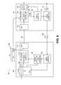
- FIG. 2Ais a block diagram of a circuit implementing error recovery modules to provide reliable data transfers at physical interfaces that use embedded clocks and clock recovery, according to one embodiment of the invention.
- an electronic device 200includes physical interfaces 210 and 230 that are composed of an RX error recovery module (“ERM”) 212 and RX error recovery module (“ERM”) 232 , respectively.
- REMRX error recovery module
- FIG. 2Aomits physical interfaces that include TX error recovery modules, an ordinarily skilled artisan should appreciate that such TX error recovery modules can also be implemented, but with inverse functionality.
- physical interfaces 210 and 230are formed as circuits within, for example, an input/output (“I/O”) ring 202 .
- I/Oinput/output
- I/O ring 202includes input and output terminals 201 for coupling conductors, such as bonding wires, to an external source of signals (not shown), such as an integrated circuit transmitting signals to a core circuit 204 .
- RX error recovery module 212 and RX error recovery module 232each are coupled to a core circuit 204 to deliver signals thereto.
- the term core circuitrefers to any kind of circuit that performs one or more core functions and can be configured to receive inputs or transmits output via physical interfaces 210 and 230 .
- core circuit 204can be formed from an intellectual property (“IP”) core, which can be expressed in a Hardware Description Language (“HDL”) code (e.g., VHDL or Verilog) or as a netlist file. Accordingly, core circuit 204 is portable and can be easily inserted into most designs benefiting from low-level layer error detection and correction provided by physical interfaces 210 and 230 .
- core circuit 204is any circuit, such as a dynamic random access memory (“DRAM”), a microcontroller or processor circuit, or any type of circuit that would benefit from implementations of error detection and corrections at physical interfaces.
- DRAMdynamic random access memory
- microcontroller or processor circuitor any type of circuit that would benefit from implementations of error detection and corrections at physical interfaces.
- low-level error detection and correctionsoperates in a manner that is transparent to core circuit 204 (i.e., physical interface error recovery need not require resources of core circuit 204 to perform error detection and/or correction).
- Physical interface 210is a serial physical interface configured to serially receive N+m encoded bits into a line decoder-error detector (“LD/ED”) 214 , which is configured to decode some or all of the N+m encoded bits to form N decoded application data bits.
- the value “m”represents the difference in the number of bits from the number of encoded data bits and the number of application data bits. For example, an 8B/10B line encoder has an m of 2, which is the difference.
- Line decoder-error detector 214operates to line decode encoded bits and then detect an error, if one is detectable. If line decoder-error detector 214 detects an error, then it instructs an error corrector (“EC”) 216 to take appropriate error recovery measures.
- ECerror corrector
- error corrector 218is configured to transmit an error indication signal 218 to an external IC or device to alert the external IC or device so it can resolve the error, such as by retransmitting the N+m encoded bits to physical interface 210 .
- physical interfaces 210 and 230provide error detection and correction for core circuit 204 without modifying core circuit 204 , thereby conserving engineering resources required to integrate either error detection or correction into core 204 .
- error corrector 218is configured to transmit an error indication signal 220 into core circuit 204 so that it can correct the error.
- core circuit 204includes application-specific logic 244 to correct any detected errors.
- error handling by application-specific logic 244 in core circuit 204therefore enables error detection and correction without requiring the transmitting IC or device (not shown) to help correct the error.
- error corrector 216 of physical interface 210can correct errors without sending either error indication signals 218 or 220 .
- the error correctorcan implement forward error correction techniques, which automatically corrects errors.
- physical interface 230can provide a chip-to-chip interface to exchange error-corrected addresses and data between the DRAM controller and the DRAM memory (i.e., core circuit 204 ) without one or more of them being modified (functionally or structurally) to implement error detection and correction.
- physical interfaces 210 and 230are formed on a first substrate, which contains an input-output (“I/O”) ring 202 .
- Core circuit 204is formed on a second substrate. If the first and second substrates are separate, then physical interfaces 210 and 230 can be packaged separately from core circuit 204 .
- physical interface 230is a parallel physical interface configured to receive N+m encoded bits into RX error recovery module 232 and then decode some or all of the N+m encoded bits to form N decoded application data bits.
- FIG. 2Aomits the details of line decoder-error detector and error corrector for RX error recovery module 232 to simplify the discussion. Note that while FIG.
- serial physical interface 210 and 230depicts physical interfaces 210 and 230 providing in-bound data bits (i.e., in-bound toward core 204 ) in an in-bound direction 287 , those same physical interfaces can provide for out-bound data bit transmissions (not shown) from core 204 in an out-bound direction 289 .
- serial physical interface 210 and parallel physical interface 230 shown in FIG. 2Aare configured to line decode in-bound data bits to, among other things, recover embedded clocks therein.
- either serial physical interface 210 or parallel physical interface 230 , or bothcan be configured to receive an external clock rather than an embedded clock.
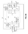
- FIG. 2Bis another block diagram of the circuit of FIG. 2A implementing error recovery modules to provide reliable data transfers at physical interfaces that use external clocks, according to one embodiment of the invention.
- electronic device 200 of FIG. 2Bincludes a serial physical interface 250 configured to receive an external clock (“Ext. CLK”) 274 .
- Electronic device 200also includes a parallel physical interface 270 configured to receive an external clock (“Ext. CLK”) 254 . Since both physical interfaces 250 and 270 can receive external clock signals, these interfaces need not include clock recovery circuits since embedded clocking techniques need not be employed. As such, error recovery modules 252 and 272 need not be disposed after a line decoder or a line decoding process. Note that elements in FIG. 2B each can have an equivalent functionality and/or structure as elements similarly-numbered in FIG. 2A .
- FIG. 3is a block diagram showing a physical interface configured to detect and optionally correct errors, according to a specific embodiment of the invention.
- a physical interface 300includes a physical layer (“PHY”) line decoder 302 and an error recovery module 310 , which is composed of an error detection bit extractor 312 , an error detector 314 and an error corrector 316 .
- Error detection bit extractor 312is at least functionally cooperative with the line decoding process of PHY line decoder 302 and, as such, it is shown in FIG. 3 to reside within PHY line decoder 302 .
- PHY line decoder 302is at least configured to receive N+m encoded bits (i.e., symbols or code words) of a bit stream and to decode all or some of those bits to form N decoded application data bits.
- PHY line decoder 302can operate to receive 10, 14, 20, 66, or 130 encoded application data bits (or “N+2” bits), and then can respectively decode those bits to form 8, 12, 18, 64 or 128 decoded application data bits (or “N” bits). The two bits are traditionally used for at least clock recovery and DC-balancing.
- PHY line decoder 302can operate to receive any number of encoded data bits and then decode those bits into any other number of application data bits. For example, PHY line decoder 302 can decode 80 bits of encoded data to form 64 decoded application data bits.
- PHY line decoder 302decodes the N+m ⁇ 1 encoded bits, which is a subset of the N+m bits, to yield N decoded application data bits and E error detection bits. Then, error detection bit extractor 312 extracts one or more physical interface error detection bits for low-level error detection purposes. For example, error detection bit extractor 312 can extract a single bit from the quantity of N+m (e.g., 10 bits) to yield N+m ⁇ 1 bits (e.g., 9 bits) decoded bits, which include N decoded application data bits and E decoded error detection bits.
- N+me.g. 10 bits
- PHY line decoder 302is configured to receive N+m bits, and to perform line decoding, which yields N application data bits and at least one error detection bit.
- PHY line decoder 302can be implemented to supplement or replace a conventional 10B/8B decoder, which uses a commonly-used symbol size of 10 bits for the encoded bits, with the decoded application data bits having a bit size of 8 bits.
- PHY line decoder 302examines a 9 th bit (i.e., one of the two bits of the difference between 10 encoded and 8 decoded application data bits) to detect errors.
- a suitable PHY line decoder 302is an N+1 bit/N bit decoder as described in U.S. Pat.
- FIG. 3depicts a PHY line decoder 302
- a PHY line encoderthat encodes N application data bits and E error detection bits into N+m encoded bits (i.e., an N bit/N+m bit encoder) can be constructed to operate in an inverse manner described in FIG. 3 and elsewhere herein.
- error detection bit extractor 312After extraction, error detection bit extractor 312 then sends the physical interface (“PI”) error detection bit (“EDB”) 313 to error detector 314 , which uses that bit to determine whether the N+m encoded data bits include one or more erroneous data bits.
- Error detector 314is configured to detect errors in accordance with any number of error detection techniques and codes. In one embodiment, error detector 314 is configured as either an even or odd parity checker, with the physical interface error detection bit being a parity bit (i.e., either an even or odd parity bit).
- the physical interface error detection bitsare received at PHY line decoder 302 concurrent with subsets of application data bits that undergo decoding.
- the physical interface error detection bitis a portion (e.g., one bit) of a CRC checksum.
- an error-detection code generator in a transmitting physical interface(not shown) is configured to generate the physical interface error detection bit as part of a CRC checksum.
- an error-detection code generator(or equivalent) can provide the bits of the CRC checksum to a PHY line encoder (not shown), which inserts the physical interface error detection bit with N unencoded application data bits to yield N+2 encoded data bits. Consequently, error detector 314 operates to accumulate or collect physical interface error detection bits from each subset of decoded N+m data bits to reconstruct the CRC checksum as an error-detection code. For example, consider that for each set of 10 encoded bits being decoded by PHY line decoder 302 , one bit of a CRC checksum is provided as a physical interface error detection bit for each set of 8 decoded application data bits.
- error detector 314can reconstruct the 16-bit CRC checksum. Then, error detector 314 generates a CRC checksum from those 128 bits and then compares that CRC checksum against the reconstructed error-detection code to determine whether an error has occurred. Error detector 314 can implement other error detection techniques, such as forward error correction. Examples of forward error correction techniques include Reed-Solomon codes, Hamming codes, and Bose-Chaudhuri-Hocquenghem (“BCH”) codes.
- BCHBose-Chaudhuri-Hocquenghem
- error detector 314determines that an error has occurred during data bit transmission, then it signals to error corrector 316 that such an error has occurred.
- error corrector 316operates to request a retransmission of the decoded application data bits for which an error has been detected.
- error corrector 316can request that the transmitting physical interface resend those 128 bits.
- error corrector 316can activate an application-specific circuit to perform user-defined error handling.
- error corrector 316can take some sort of default error-correcting action, such as reinitializing an associated IC, like a core circuit described above.
- FIG. 4is a functional block diagram illustrating line encoding in a transmitter and line decoding in a receiver with error-detection bit insertion and extraction, according to one embodiment of the invention.
- transmitter physical interface (“TX”) 410includes a PHY line encoder 412 , an error detection code generator 416 , an error bit inserter 418 and an optional buffer 421 for maintaining application data bits during generation of error detection codes, for example.
- error detection code generator 416generates an error detection code based on application data bits in buffer 421 , such as a 16-bit CRC checksum.
- an error bit inserter 418selects at least one error-detection bit (“EDB”) 414 from the 16-bit CRC checksum and then inserts it with an out-going set of N application data bits from buffer 421 to form 9 bits.
- PHY line encoder 412encodes the 9 bits into 10 encoded bits (or symbols).
- PHY line encoder 412encodes error-detection bit 414 in a manner that embeds an asynchronous clock in the 10 encoded bits as well as maintaining a zero DC offset and/or optimal spectral characteristics for those same encoded bits.
- PHY line encoder 412operates in accordance with coding techniques set forth in U.S. Pat. No.
- PHY line encoder 412encodes the N bits of application data into N+1 encoded bits.
- Nis the number 9.
- PHY line encoder 412can encode 8 application data bits and 1 error bit (i.e., 9 bits) into 10 encoded bits without affecting the data rate associated with 8B/10B coding schemes. Note that in FIG. 4 , N can represent any non-negative integer.
- Transmitter physical interface 410then sends the encoded bits via physical medium 420 to error bit extractor 422 of a receiving physical interface (“RX”) 440 .
- Receiving physical interface (“RX”) 440includes a PHY line decoder 428 , an error bit extractor 422 , error detection code reconstructor 426 , an error detector 430 , a comparator 434 , and a buffer 431 , which can maintain the decoded application data bits pending confirmation that no errors are detected.
- PHY line decoder 428decodes the 10 encoded data bits into 9 decoded bits, which includes 8 decoded application data bits and 1 decoded error detection bit (“EDB”) 424 .
- EDBdecoded error detection bit
- PHY line decoder 428includes clock data recovery circuits (not shown) to recover the embedded clock transmitted over physical medium 420 with the encoded application data bits.
- Error bit extractor 422extracts error-detection bit 424 from the 9 decoded bits and provide it to error detection code reconstructor 426 , which accumulates the error detection bit with other physical interface error detection bits.
- error detection code reconstructor 426reconstructs the error detection code, which was originally generated by error detection code generator 416 .
- error detector 430generates a CRC checksum 432 based on a group of N decoded application data bits in buffer 431 .
- comparator 434can operate to compare whether CRC checksum 432 matches error detection code 426 . If it does, then there is no error; if it does not, then there is an error.
- FIG. 5depicts one example of a flow for line encoding a group of data bits as a cell in accordance with one embodiment of the invention.
- a transmitting physical interfacecan transmit data as shown in flow 550 , whereby groups 560 of data bits can be referred to as a cell (as well as a frame or the like).
- Cell 560can include any number of control bits 561 (e.g., x number of bits) and two application data words 563 of 64 bits each.
- An upper-layer device(not shown), which resides above a PHY line encoder in the physical layer, can be configured to break cell 560 into discrete sets 562 of uncoded (i.e., precoded or unencoded) bits for use by a PHY line encoder. Each set 562 has N bits (e.g., 8 bits).
- An error detection code generator(not shown) generates an error detection code 570 based on cell 560 to form an error detection code as a 12-bit CRC, for example.
- the PHY line encoderthen can insert a physical interface error detection bit (“EDB”) 572 into the uncoded bit stream in or near sets 562 to form sets 574 of N+E bits (e.g., N can be 8 bits and E can be 1 bit).
- EDBphysical interface error detection bit
- the PHY line encoderthen can translate each set 572 of N+E bits into 10-bit code words 580 (e.g., encoded data bits) for transmission over a data link, such as a serial data link.
- a PHY line decoder at a receiving physical interfacewould operate in a similar, but inverse manner.
- FIG. 6is a block diagram 600 illustrating physical interfaces that provide for error detection and correction by at least retransmitting data bits, according to at least one specific embodiment of the invention.
- Physical interfaces 602 and 652provide for physical connectivity through a high-speed serial communications link 650 .
- Physical interface 602includes storage, such as a first in, first out buffer (“FIFO”) 604 , for storing data bits that are to be transmitted.
- FIFO 604maintains the stored data bits to compute, for example, an error detection code over a group of data bits. In some cases, FIFO 604 stores data bits for retransmission if an error occurs.
- FIFOfirst in, first out buffer
- Physical interface 602also includes PHY line encoder (“PHY encoder”) 610 , a serializer (“SER”) 612 for serializing parallel data bits, an error-detection code generator 616 and a transmitter (“TX”) error corrector 618 .
- PHY line encoder(“PHY encoder”) 610
- SERserializer
- TXtransmitter
- error detection code generator 616Based on the contents of the group of data bits in FIFO 604 at a specific time, error detection code generator 616 generates an error detection code, such as a CRC checksum.
- Error detection bit inserter 614decomposes the CRC checksum and inserts at least one bit (e.g., one E bit) as a physical interface error detection bit (“EDB”) with the N unencoded bits 606 .
- EDBphysical interface error detection bit
- PHY line encoder 610encodes N+E bits to form N+2 encoded data bits 608 .
- Serializer 612then serializes N+2 data bits 608 prior to transmission over link 650 .
- Receiving physical interface 652includes a deserializer 654 to convert N+2 data bits 608 to parallel data bits.
- PHY line decoder (“PHY decoder”) 656decodes the encoded bits stream and stores the decoded data bits in FIFO 658 .
- Error detection bit (“EDB”) extractor 660extracts at least one bit as physical interface error detection bit (“EDB”) 662 and sends it to error detector 666 . When error code reconstruction is complete, error detector 666 operates to determine whether an error has occurred.
- PHY line decoder(“PHY decoder”) 656 decodes the encoded bits stream and stores the decoded data bits in FIFO 658 .
- Error detection bit (“EDB”) extractor 660extracts at least one bit as physical interface error
- error detector 666If error detector 666 detects no errors, then it instructs FIFO 658 to release the decoded data bits for further processing. But if error detector 666 detects an error, then it indicates the presence of an error to a receiver (“RX”) error corrector 668 .
- RX error corrector 668sends a request 669 to instruct TX error corrector 618 to retransmit the contents, or a portion thereof, via link 650 .
- RX error corrector 668can send a request 671 to an application-specific circuit (not shown) to handle the error.
- receiver error corrector 668can correct the error using forward error correction techniques or the like.
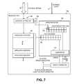
- FIG. 7illustrates an alternative receiver for implementing error detection and correction without line decoding, according to at least one specific embodiment of the invention.
- receiver (“RX”) 700a transmitting physical interface (not shown) sends data bits via link 702 .
- Error bit extractor 704extracts error detection data bits (“EDBs”) 706 from the data bits and collects them to reconstruct an error detection code 708 .
- EDBserror detection data bits
- receiver 700does not use a PHY line decoder as does receiver 440 . As such, receiver 700 need not recover a clock signal from an embedded clock.
- receiver 700is configured to receive an external clock 701 from, for example, a transmitting device (not shown).
- Receiver 700includes an error detector 780 for computing an error detection code, or in this case, a CRC checksum 722 based on a group of application data bits in FIFO 720 .
- a comparator 724e.g., in error detector 720 ) then determines whether a transmission error has occurred. If an error exists, then an error corrector 780 can take corrective action by, for example, either requesting the transmitting device to retransmit the data bits or signaling application-specific logic that it is to correct the error.
- FIG. 8depicts a block diagram of an error corrector according to one embodiment of the invention.
- Error corrector 800 in this exampleincludes an error corrector controller 822 to control one or more functions that can resolve errors, with the specific functions being programmed by a user for specific applications. For example, loss of pixel data in video memory application is not as crucial as the loss of data in other applications. As such, error corrector controller 822 can select any of the following modules to implement error correction.
- Retransmission request module 824generates a request bound for the transmitting physical interface to resend the data bits upon detection of an error.
- Application-specific recovery module 814signals an application-specific circuit to initiate its custom error-handling routines, as prescribed by a designer.
- error corrector controller 822can select a default error recovery scheme, such as reinitializing an IC upon detection of an error. This will cause both physical interfaces to reinitialize to a known state.
- error corrector 800can include a frequency selector 830 , an amplitude selector 840 , and a coding selector 850 . If signals on the communication link between the physical interfaces falter, then frequency selector 830 can adjust the data transfer rate over the link to reduce the error rate. Or, amplitude selector 840 can adjust the signal amplitude until the error rate is curtailed. Coding selector 850 can be used to change the line coding, for example, from 18B/20B to 8B/10B to reduce the time during which errors are detected.
- coding selector 850can increase the rate at which errors codes (e.g., CRCs) are transmitted over a communications channel. Error corrector controller 822 can chose these selectors individually or in combination.
Landscapes
- Engineering & Computer Science (AREA)
- Computer Networks & Wireless Communication (AREA)
- Signal Processing (AREA)
- Computer Security & Cryptography (AREA)
- Physics & Mathematics (AREA)
- Spectroscopy & Molecular Physics (AREA)
- Detection And Prevention Of Errors In Transmission (AREA)
- Detection And Correction Of Errors (AREA)
- Data Exchanges In Wide-Area Networks (AREA)
- Dc Digital Transmission (AREA)
Abstract
Description
Claims (16)
Priority Applications (1)
| Application Number | Priority Date | Filing Date | Title |
|---|---|---|---|
| US13/099,254US8099648B2 (en) | 2006-03-09 | 2011-05-02 | Error detection in physical interfaces for point-to-point communications between integrated circuits |
Applications Claiming Priority (3)
| Application Number | Priority Date | Filing Date | Title |
|---|---|---|---|
| US11/372,866US7694204B2 (en) | 2006-03-09 | 2006-03-09 | Error detection in physical interfaces for point-to-point communications between integrated circuits |
| US12/712,124US7937644B2 (en) | 2006-03-09 | 2010-02-24 | Error detection in physical interfaces for point-to-point communications between integrated circuits |
| US13/099,254US8099648B2 (en) | 2006-03-09 | 2011-05-02 | Error detection in physical interfaces for point-to-point communications between integrated circuits |
Related Parent Applications (1)
| Application Number | Title | Priority Date | Filing Date |
|---|---|---|---|
| US12/712,124DivisionUS7937644B2 (en) | 2006-03-09 | 2010-02-24 | Error detection in physical interfaces for point-to-point communications between integrated circuits |
Publications (2)
| Publication Number | Publication Date |
|---|---|
| US20110209027A1 US20110209027A1 (en) | 2011-08-25 |
| US8099648B2true US8099648B2 (en) | 2012-01-17 |
Family
ID=38190575
Family Applications (3)
| Application Number | Title | Priority Date | Filing Date |
|---|---|---|---|
| US11/372,866Active2029-01-21US7694204B2 (en) | 2006-03-09 | 2006-03-09 | Error detection in physical interfaces for point-to-point communications between integrated circuits |
| US12/712,124ActiveUS7937644B2 (en) | 2006-03-09 | 2010-02-24 | Error detection in physical interfaces for point-to-point communications between integrated circuits |
| US13/099,254ActiveUS8099648B2 (en) | 2006-03-09 | 2011-05-02 | Error detection in physical interfaces for point-to-point communications between integrated circuits |
Family Applications Before (2)
| Application Number | Title | Priority Date | Filing Date |
|---|---|---|---|
| US11/372,866Active2029-01-21US7694204B2 (en) | 2006-03-09 | 2006-03-09 | Error detection in physical interfaces for point-to-point communications between integrated circuits |
| US12/712,124ActiveUS7937644B2 (en) | 2006-03-09 | 2010-02-24 | Error detection in physical interfaces for point-to-point communications between integrated circuits |
Country Status (6)
| Country | Link |
|---|---|
| US (3) | US7694204B2 (en) |
| EP (1) | EP1833188B1 (en) |
| JP (2) | JP2007267392A (en) |
| KR (2) | KR101363704B1 (en) |
| CN (2) | CN103401636B (en) |
| TW (1) | TWI369093B (en) |
Cited By (4)
| Publication number | Priority date | Publication date | Assignee | Title |
|---|---|---|---|---|
| US20110026544A1 (en)* | 2009-07-30 | 2011-02-03 | Stmicroelectronics S.R.L. | Signals communication apparatus |
| US20160147596A1 (en)* | 2014-11-26 | 2016-05-26 | Qualcomm Incorporated | Error detection constants of symbol transition clocking transcoding |
| US9779341B2 (en) | 2015-05-18 | 2017-10-03 | Canon Kabushiki Kaisha | Data communication system, data transmission apparatus, and data reception apparatus |
| US9892483B2 (en) | 2013-11-13 | 2018-02-13 | Samsung Electronics Co., Ltd. | Timing controller, display system including the same, and method of use thereof |
Families Citing this family (112)
| Publication number | Priority date | Publication date | Assignee | Title |
|---|---|---|---|---|
| JP4949707B2 (en)* | 2006-03-22 | 2012-06-13 | ルネサスエレクトロニクス株式会社 | Semiconductor device and test method thereof |
| KR100763207B1 (en)* | 2006-05-03 | 2007-10-04 | 삼성전자주식회사 | Method, apparatus, and transmission frame structure for transmitting and receiving uncompressed AV data |
| JP4783245B2 (en)* | 2006-09-01 | 2011-09-28 | 株式会社日立製作所 | Transceiver, transmitter, and receiver |
| US8223628B2 (en)* | 2007-01-10 | 2012-07-17 | Lantiq Deutschland Gmbh | Data transmission method, transmitter, receiver, transceiver and transmission system |
| US8565337B2 (en)* | 2007-02-07 | 2013-10-22 | Valens Semiconductor Ltd. | Devices for transmitting digital video and data over the same wires |
| TWI365615B (en)* | 2007-03-22 | 2012-06-01 | Realtek Semiconductor Corp | Receiver of a displayport interface having an error correction circuit and method applied to the receiver |
| US7568137B1 (en)* | 2007-03-27 | 2009-07-28 | Xilinx, Inc. | Method and apparatus for a clock and data recovery circuit |
| US9686045B2 (en)* | 2007-04-04 | 2017-06-20 | Lantiq Beteiligungs-GmbH & Co. KG | Data transmission and retransmission |
| US8296621B2 (en)* | 2007-04-04 | 2012-10-23 | Freescale Semiconductor, Inc. | Integrated circuit comprising error correction logic, and a method of error correction |
| JP2009130614A (en)* | 2007-11-22 | 2009-06-11 | Fujitsu Ltd | COMMUNICATION CONTROL DEVICE, COMMUNICATION CONTROL METHOD, AND COMMUNICATION CONTROL PROGRAM |
| US7783819B2 (en) | 2008-03-31 | 2010-08-24 | Intel Corporation | Integrating non-peripheral component interconnect (PCI) resources into a personal computer system |
| JP5233415B2 (en)* | 2008-05-29 | 2013-07-10 | 富士通株式会社 | Error identification method, data processing apparatus, and semiconductor device |
| US8572187B2 (en)* | 2009-04-27 | 2013-10-29 | International Business Machines Corporation | Automated duplicate message content detection |
| US8948286B2 (en)* | 2009-10-20 | 2015-02-03 | Wisconsin Alumni Research Foundation | Wireless communication system mapping data bits to symbol bit positions according to error rates of those bit positions and data content |
| US8930799B1 (en)* | 2010-03-03 | 2015-01-06 | Aquantia Corp. | Methods and apparatus for correcting block-coded data errors with an error detection code |
| US9288089B2 (en) | 2010-04-30 | 2016-03-15 | Ecole Polytechnique Federale De Lausanne (Epfl) | Orthogonal differential vector signaling |
| US9251873B1 (en) | 2010-05-20 | 2016-02-02 | Kandou Labs, S.A. | Methods and systems for pin-efficient memory controller interface using vector signaling codes for chip-to-chip communications |
| US9077386B1 (en) | 2010-05-20 | 2015-07-07 | Kandou Labs, S.A. | Methods and systems for selection of unions of vector signaling codes for power and pin efficient chip-to-chip communication |
| US9106238B1 (en) | 2010-12-30 | 2015-08-11 | Kandou Labs, S.A. | Sorting decoder |
| US9288082B1 (en) | 2010-05-20 | 2016-03-15 | Kandou Labs, S.A. | Circuits for efficient detection of vector signaling codes for chip-to-chip communication using sums of differences |
| US9450744B2 (en) | 2010-05-20 | 2016-09-20 | Kandou Lab, S.A. | Control loop management and vector signaling code communications links |
| US9985634B2 (en) | 2010-05-20 | 2018-05-29 | Kandou Labs, S.A. | Data-driven voltage regulator |
| US9596109B2 (en) | 2010-05-20 | 2017-03-14 | Kandou Labs, S.A. | Methods and systems for high bandwidth communications interface |
| US9362962B2 (en) | 2010-05-20 | 2016-06-07 | Kandou Labs, S.A. | Methods and systems for energy-efficient communications interface |
| US8593305B1 (en) | 2011-07-05 | 2013-11-26 | Kandou Labs, S.A. | Efficient processing and detection of balanced codes |
| US9564994B2 (en) | 2010-05-20 | 2017-02-07 | Kandou Labs, S.A. | Fault tolerant chip-to-chip communication with advanced voltage |
| US9401828B2 (en) | 2010-05-20 | 2016-07-26 | Kandou Labs, S.A. | Methods and systems for low-power and pin-efficient communications with superposition signaling codes |
| US9300503B1 (en) | 2010-05-20 | 2016-03-29 | Kandou Labs, S.A. | Methods and systems for skew tolerance in and advanced detectors for vector signaling codes for chip-to-chip communication |
| US9124557B2 (en) | 2010-05-20 | 2015-09-01 | Kandou Labs, S.A. | Methods and systems for chip-to-chip communication with reduced simultaneous switching noise |
| US9479369B1 (en) | 2010-05-20 | 2016-10-25 | Kandou Labs, S.A. | Vector signaling codes with high pin-efficiency for chip-to-chip communication and storage |
| US9246713B2 (en) | 2010-05-20 | 2016-01-26 | Kandou Labs, S.A. | Vector signaling with reduced receiver complexity |
| US9071476B2 (en) | 2010-05-20 | 2015-06-30 | Kandou Labs, S.A. | Methods and systems for high bandwidth chip-to-chip communications interface |
| WO2011151469A1 (en) | 2010-06-04 | 2011-12-08 | Ecole Polytechnique Federale De Lausanne | Error control coding for orthogonal differential vector signaling |
| US9306769B2 (en)* | 2010-10-05 | 2016-04-05 | Mellanox Technologies Tlv Ltd. | Cell-based link-level retry scheme |
| US8750176B2 (en) | 2010-12-22 | 2014-06-10 | Apple Inc. | Methods and apparatus for the intelligent association of control symbols |
| US9275720B2 (en) | 2010-12-30 | 2016-03-01 | Kandou Labs, S.A. | Differential vector storage for dynamic random access memory |
| US8457153B2 (en)* | 2011-04-04 | 2013-06-04 | Cisco Technology, Inc. | HDMI-SFP+ adapter/extender |
| US9577788B2 (en)* | 2011-06-15 | 2017-02-21 | Denso Corporation | Coding apparatus, coding method, data communication apparatus, and data communication method |
| WO2013076532A1 (en)* | 2011-11-25 | 2013-05-30 | Freescale Semiconductor, Inc. | Controller, sata system and method of operation therefor |
| US8897398B2 (en) | 2012-01-27 | 2014-11-25 | Apple Inc. | Methods and apparatus for error rate estimation |
| US9838226B2 (en) | 2012-01-27 | 2017-12-05 | Apple Inc. | Methods and apparatus for the intelligent scrambling of control symbols |
| US9268683B1 (en) | 2012-05-14 | 2016-02-23 | Kandou Labs, S.A. | Storage method and apparatus for random access memory using codeword storage |
| JP6069897B2 (en) | 2012-06-05 | 2017-02-01 | 富士通株式会社 | Data transmission apparatus and data transmission method |
| EP2685645B1 (en)* | 2012-07-09 | 2016-04-27 | Alcatel Lucent | Methods and device for processing digital data frames and transport frames for reduction of transport bandwidth |
| US9262270B2 (en)* | 2012-12-28 | 2016-02-16 | Intel Corporation | Live error recovery |
| US9450790B2 (en) | 2013-01-31 | 2016-09-20 | Apple Inc. | Methods and apparatus for enabling and disabling scrambling of control symbols |
| WO2014124450A1 (en)* | 2013-02-11 | 2014-08-14 | Kandou Labs, S.A. | Methods and systems for high bandwidth chip-to-chip communications interface |
| US9455745B2 (en)* | 2013-02-21 | 2016-09-27 | Microsoft Technology Licensing, Llc | Encoding with integrated error-detection |
| US9210010B2 (en) | 2013-03-15 | 2015-12-08 | Apple, Inc. | Methods and apparatus for scrambling symbols over multi-lane serial interfaces |
| CN110166217B (en) | 2013-04-16 | 2022-05-17 | 康杜实验室公司 | High bandwidth communication interface method and system |
| US9344901B2 (en)* | 2013-04-16 | 2016-05-17 | Qualcomm Incorporated | Apparatus and methods of processing a protocol data unit |
| EP2997704B1 (en) | 2013-06-25 | 2020-12-16 | Kandou Labs S.A. | Vector signaling with reduced receiver complexity |
| US9274880B1 (en)* | 2013-08-09 | 2016-03-01 | Altera Corporation | Methods and apparatus for detecting and correcting errors in high-speed serial communications systems |
| US9106465B2 (en) | 2013-11-22 | 2015-08-11 | Kandou Labs, S.A. | Multiwire linear equalizer for vector signaling code receiver |
| WO2015083563A1 (en)* | 2013-12-04 | 2015-06-11 | ソニー株式会社 | Browser device, recording medium, server device, and information processing method |
| US9397792B2 (en)* | 2013-12-06 | 2016-07-19 | Intel Corporation | Efficient link layer retry protocol utilizing implicit acknowledgements |
| US9325449B2 (en) | 2013-12-06 | 2016-04-26 | Intel Corporation | Lane error detection and lane removal mechanism to reduce the probability of data corruption |
| US9806761B1 (en) | 2014-01-31 | 2017-10-31 | Kandou Labs, S.A. | Methods and systems for reduction of nearest-neighbor crosstalk |
| US9100232B1 (en) | 2014-02-02 | 2015-08-04 | Kandou Labs, S.A. | Method for code evaluation using ISI ratio |
| US9369312B1 (en) | 2014-02-02 | 2016-06-14 | Kandou Labs, S.A. | Low EMI signaling for parallel conductor interfaces |
| US9270415B2 (en)* | 2014-02-03 | 2016-02-23 | Valens Semiconductor Ltd. | Encoding payloads according to data types while maintaining running disparity |
| KR102108380B1 (en) | 2014-02-04 | 2020-05-08 | 삼성전자주식회사 | Interface circuit operating to recover transmitted data error |
| KR102240544B1 (en) | 2014-02-28 | 2021-04-19 | 칸도우 랩스 에스에이 | Clock-embedded vector signaling codes |
| US9319178B2 (en) | 2014-03-14 | 2016-04-19 | Qualcomm Incorporated | Method for using error correction codes with N factorial or CCI extension |
| US20150326884A1 (en)* | 2014-05-12 | 2015-11-12 | Silicon Image, Inc. | Error Detection and Mitigation in Video Channels |
| US9509437B2 (en) | 2014-05-13 | 2016-11-29 | Kandou Labs, S.A. | Vector signaling code with improved noise margin |
| US9148087B1 (en) | 2014-05-16 | 2015-09-29 | Kandou Labs, S.A. | Symmetric is linear equalization circuit with increased gain |
| US9852806B2 (en) | 2014-06-20 | 2017-12-26 | Kandou Labs, S.A. | System for generating a test pattern to detect and isolate stuck faults for an interface using transition coding |
| US9112550B1 (en) | 2014-06-25 | 2015-08-18 | Kandou Labs, SA | Multilevel driver for high speed chip-to-chip communications |
| EP3138253A4 (en) | 2014-07-10 | 2018-01-10 | Kandou Labs S.A. | Vector signaling codes with increased signal to noise characteristics |
| US9432082B2 (en) | 2014-07-17 | 2016-08-30 | Kandou Labs, S.A. | Bus reversable orthogonal differential vector signaling codes |
| KR101943048B1 (en) | 2014-07-21 | 2019-01-28 | 칸도우 랩스 에스에이 | Multidrop data transfer |
| WO2016019384A1 (en) | 2014-08-01 | 2016-02-04 | Kandou Labs, S.A. | Orthogonal differential vector signaling codes with embedded clock |
| US9674014B2 (en) | 2014-10-22 | 2017-06-06 | Kandou Labs, S.A. | Method and apparatus for high speed chip-to-chip communications |
| US12413262B2 (en)* | 2014-11-19 | 2025-09-09 | Maxlinear, Inc. | Link loss detection |
| US9921899B2 (en)* | 2014-12-18 | 2018-03-20 | Oracle International Corporation | Monitoring serial link errors |
| GB2539443B (en)* | 2015-06-16 | 2020-02-12 | Advanced Risc Mach Ltd | A transmitter, a receiver, a data transfer system and a method of data transfer |
| KR101978470B1 (en) | 2015-06-26 | 2019-05-14 | 칸도우 랩스 에스에이 | High-speed communication system |
| US10367605B2 (en)* | 2015-07-02 | 2019-07-30 | Intel Corporation | High speed interconnect symbol stream forward error-correction |
| JP6657690B2 (en)* | 2015-09-10 | 2020-03-04 | 富士ゼロックス株式会社 | Decoding device, program, and information transmission system |
| US9557760B1 (en) | 2015-10-28 | 2017-01-31 | Kandou Labs, S.A. | Enhanced phase interpolation circuit |
| US9577815B1 (en) | 2015-10-29 | 2017-02-21 | Kandou Labs, S.A. | Clock data alignment system for vector signaling code communications link |
| US10055372B2 (en) | 2015-11-25 | 2018-08-21 | Kandou Labs, S.A. | Orthogonal differential vector signaling codes with embedded clock |
| US10003315B2 (en) | 2016-01-25 | 2018-06-19 | Kandou Labs S.A. | Voltage sampler driver with enhanced high-frequency gain |
| EP3446403B1 (en) | 2016-04-22 | 2021-01-06 | Kandou Labs S.A. | High performance phase locked loop |
| US10003454B2 (en) | 2016-04-22 | 2018-06-19 | Kandou Labs, S.A. | Sampler with low input kickback |
| US10056903B2 (en) | 2016-04-28 | 2018-08-21 | Kandou Labs, S.A. | Low power multilevel driver |
| EP3449379B1 (en) | 2016-04-28 | 2021-10-06 | Kandou Labs S.A. | Vector signaling codes for densely-routed wire groups |
| US10153591B2 (en) | 2016-04-28 | 2018-12-11 | Kandou Labs, S.A. | Skew-resistant multi-wire channel |
| US9906358B1 (en) | 2016-08-31 | 2018-02-27 | Kandou Labs, S.A. | Lock detector for phase lock loop |
| US10411922B2 (en) | 2016-09-16 | 2019-09-10 | Kandou Labs, S.A. | Data-driven phase detector element for phase locked loops |
| US10200259B1 (en)* | 2016-09-21 | 2019-02-05 | Symantec Corporation | Systems and methods for detecting obscure cyclic application-layer message sequences in transport-layer message sequences |
| US10200188B2 (en) | 2016-10-21 | 2019-02-05 | Kandou Labs, S.A. | Quadrature and duty cycle error correction in matrix phase lock loop |
| US10372665B2 (en) | 2016-10-24 | 2019-08-06 | Kandou Labs, S.A. | Multiphase data receiver with distributed DFE |
| US10200218B2 (en) | 2016-10-24 | 2019-02-05 | Kandou Labs, S.A. | Multi-stage sampler with increased gain |
| EP3322203B1 (en)* | 2016-11-13 | 2020-05-20 | Harman International Industries, Incorporated | Fault tolerant network audio system |
| DE102016014375B4 (en)* | 2016-12-03 | 2018-06-21 | Diehl Metering Systems Gmbh | Method for improving the transmission quality between a data collector and a plurality of autonomous measuring units and communication system |
| EP4216444B1 (en) | 2017-04-14 | 2025-08-27 | Kandou Labs SA | Pipelined forward error correction for vector signaling code channel |
| US10116468B1 (en) | 2017-06-28 | 2018-10-30 | Kandou Labs, S.A. | Low power chip-to-chip bidirectional communications |
| US10686583B2 (en) | 2017-07-04 | 2020-06-16 | Kandou Labs, S.A. | Method for measuring and correcting multi-wire skew |
| US10693587B2 (en) | 2017-07-10 | 2020-06-23 | Kandou Labs, S.A. | Multi-wire permuted forward error correction |
| US10203226B1 (en) | 2017-08-11 | 2019-02-12 | Kandou Labs, S.A. | Phase interpolation circuit |
| US10326623B1 (en) | 2017-12-08 | 2019-06-18 | Kandou Labs, S.A. | Methods and systems for providing multi-stage distributed decision feedback equalization |
| US10554380B2 (en) | 2018-01-26 | 2020-02-04 | Kandou Labs, S.A. | Dynamically weighted exclusive or gate having weighted output segments for phase detection and phase interpolation |
| CN108847915B (en)* | 2018-05-29 | 2020-11-24 | 北京光润通科技发展有限公司 | Method for realizing unidirectional transmission by reconstructing source end data by applying error correction coding technology |
| US10498567B1 (en)* | 2018-11-26 | 2019-12-03 | Xilinx, Inc. | Die-to-die communications scheme |
| US10630314B1 (en)* | 2019-06-18 | 2020-04-21 | Nxp B.V. | Method and system for asynchronous serialization of multiple serial communication signals |
| US11356197B1 (en) | 2021-03-19 | 2022-06-07 | Kandou Labs SA | Error-tolerant forward error correction ordered set message decoder |
| US11947810B2 (en) | 2021-04-07 | 2024-04-02 | Samsung Electronics Co., Ltd. | Semiconductor memory device and memory system including the same |
| WO2023121649A1 (en)* | 2021-12-20 | 2023-06-29 | Zeku, Inc. | Apparatus and method for on-chip communication of a baseband chip |
| US12149348B2 (en)* | 2022-11-15 | 2024-11-19 | Xilinx, Inc. | Fast clock domain crossing architecture for high frequency trading (HFT) |
| WO2025110715A1 (en)* | 2023-11-21 | 2025-05-30 | 삼성전자 주식회사 | Keyboard device and electronic device connected to keyboard device |
Citations (24)
| Publication number | Priority date | Publication date | Assignee | Title |
|---|---|---|---|---|
| US5923680A (en) | 1997-06-05 | 1999-07-13 | Northern Telecom Limited | Error correction in a digital transmission system |
| US5974544A (en)* | 1991-12-17 | 1999-10-26 | Dell Usa, L.P. | Method and controller for defect tracking in a redundant array |
| US6292517B1 (en)* | 1998-09-15 | 2001-09-18 | Tut Systems, Inc. | Method and apparatus for detecting a data signal on a carrier medium |
| US6324669B1 (en)* | 1997-11-17 | 2001-11-27 | Seagate Technology Llc | Method and apparatus for using CRC for data integrity in on-chip memory |
| US6421803B1 (en) | 1999-06-25 | 2002-07-16 | Telefonaktiebolaget L M Ericsson (Publ) | System and method for implementing hybrid automatic repeat request using parity check combining |
| US20030070132A1 (en) | 2001-08-16 | 2003-04-10 | Christopher Pasqualino | Flexible video encoding scheme supporting audio and auxiliary information |
| US6594262B1 (en) | 1997-11-28 | 2003-07-15 | Electronics And Telecommunications Research Institute | Apparatus and method for protecting ATM header from the burst error |
| US20030185251A1 (en) | 2002-03-28 | 2003-10-02 | Nec Corporation | Multiplex transmission system capable of using ordinary network packets to transmit a plurality of 8B/10B bit streams |
| EP1351462A1 (en) | 2002-03-29 | 2003-10-08 | MystiCom, Ltd. | Error Correcting 8B/10B Transmission System |
| US6662332B1 (en) | 2000-07-05 | 2003-12-09 | 3Com Corporation | Interleaver for burst error correction |
| US20030237041A1 (en) | 2002-06-25 | 2003-12-25 | Cole Robert M. | System and method for transferring data on a data link |
| US6735217B1 (en)* | 1998-09-15 | 2004-05-11 | Tut Systems, Inc. | Method and apparatus for detecting collisions on a network using multi-cycle waveform pulses |
| US6747580B1 (en) | 2003-06-12 | 2004-06-08 | Silicon Image, Inc. | Method and apparatus for encoding or decoding data in accordance with an NB/(N+1)B block code, and method for determining such a block code |
| CN2662571Y (en) | 2001-08-24 | 2004-12-08 | 交互数字技术公司 | Single-Carrier Frequency-Domain Equalization (SC-FDE) subscriber equipment with automatic physical layer request retransmission mechanism |
| US20050005189A1 (en) | 2002-04-25 | 2005-01-06 | Lior Khermosh | Forward error correction coding in ethernet networks |
| US20060041820A1 (en) | 2004-08-20 | 2006-02-23 | Ling Hang | Method and apparatus for receiving a control channel in a wireless communication system |
| US7010607B1 (en)* | 1999-09-15 | 2006-03-07 | Hewlett-Packard Development Company, L.P. | Method for training a communication link between ports to correct for errors |
| US7111220B1 (en) | 2002-03-01 | 2006-09-19 | Xilinx, Inc. | Network physical layer with embedded multi-standard CRC generator |
| US20070157060A1 (en) | 2006-01-04 | 2007-07-05 | Ganga Ilango S | Techniques to perform forward error correction for an electrical backplane |
| US7248587B1 (en)* | 2005-04-11 | 2007-07-24 | Azul Systems, Inc. | Error recovery of variable-length packets without sequence numbers or special symbols used for synchronizing transmit retry-buffer pointer |
| US7280293B2 (en)* | 2005-07-18 | 2007-10-09 | International Business Machines Corporation | Multi-level mapping of tape error recoveries |
| US7430261B2 (en) | 2002-04-16 | 2008-09-30 | Robert Bosch Gmbh | Method and bit stream decoding unit using majority voting |
| US7499500B2 (en) | 2003-03-21 | 2009-03-03 | Sony United Kingdom Limited | Data communication system, method and apparatus for communicating a data signal formed of successive data elements |
| US7519084B2 (en)* | 2003-11-19 | 2009-04-14 | Mitsubishi Denki Kabushiki Kaisha | Error control mechanism for a segment based link layer in a digital network |
Family Cites Families (12)
| Publication number | Priority date | Publication date | Assignee | Title |
|---|---|---|---|---|
| JPH06103222A (en)* | 1992-04-21 | 1994-04-15 | Nec Corp | Bus transfer system |
| KR19990038709U (en)* | 1998-03-31 | 1999-10-25 | 전주범 | Error Detection Device Using Parit Bits |
| JP2000092033A (en)* | 1998-09-14 | 2000-03-31 | Nec Corp | High speed data transmission reception system |
| CN1968053B (en)* | 2000-04-17 | 2012-08-15 | 北方电讯网络有限公司 | Automatic retransmission request protocol cooperation in a wireless network |
| JP3535074B2 (en)* | 2000-04-20 | 2004-06-07 | 日本電信電話株式会社 | Control information encoding and decoding methods and control information transmitter and receiver |
| JP2002152163A (en)* | 2000-11-13 | 2002-05-24 | Fujitsu Ltd | Communication node and communication unit |
| CN1225875C (en)* | 2001-09-29 | 2005-11-02 | 华为技术有限公司 | Method of realizing data retransmission on high speed medium access control layer (MAC-HS) |
| EP1508991A1 (en)* | 2002-05-29 | 2005-02-23 | Mitsubishi Denki Kabushiki Kaisha | Data error control method |
| AU2003263421A1 (en)* | 2002-09-20 | 2004-04-08 | Koninklijke Philips Electronics N.V. | Resource reservation in transmission networks |
| JP2004328434A (en)* | 2003-04-25 | 2004-11-18 | Dds:Kk | Packet communication system and device |
| JP2005025587A (en)* | 2003-07-04 | 2005-01-27 | Matsushita Electric Ind Co Ltd | Semiconductor integrated circuit and burst transfer method in semiconductor integrated circuit |
| US7685496B2 (en)* | 2003-11-14 | 2010-03-23 | Hitachi, Ltd. | Data transmission method and data transmission device for transmitting data through a transmission line that is integrated with a plurality of links |
- 2006
- 2006-03-09USUS11/372,866patent/US7694204B2/enactiveActive
- 2007
- 2007-03-02TWTW096107301Apatent/TWI369093B/enactive
- 2007-03-08CNCN201310286497.3Apatent/CN103401636B/enactiveActive
- 2007-03-08CNCN200710087760.0Apatent/CN101035141B/enactiveActive
- 2007-03-09JPJP2007101084Apatent/JP2007267392A/enactivePending
- 2007-03-09EPEP07250987.0Apatent/EP1833188B1/enactiveActive
- 2007-03-09KRKR1020070023561Apatent/KR101363704B1/enactiveActive
- 2010
- 2010-02-24USUS12/712,124patent/US7937644B2/enactiveActive
- 2011
- 2011-05-02USUS13/099,254patent/US8099648B2/enactiveActive
- 2013
- 2013-04-10JPJP2013082428Apatent/JP2013146105A/enactivePending
- 2013-11-25KRKR1020130144144Apatent/KR101367015B1/enactiveActive
Patent Citations (25)
| Publication number | Priority date | Publication date | Assignee | Title |
|---|---|---|---|---|
| US5974544A (en)* | 1991-12-17 | 1999-10-26 | Dell Usa, L.P. | Method and controller for defect tracking in a redundant array |
| US5923680A (en) | 1997-06-05 | 1999-07-13 | Northern Telecom Limited | Error correction in a digital transmission system |
| US6324669B1 (en)* | 1997-11-17 | 2001-11-27 | Seagate Technology Llc | Method and apparatus for using CRC for data integrity in on-chip memory |
| US6594262B1 (en) | 1997-11-28 | 2003-07-15 | Electronics And Telecommunications Research Institute | Apparatus and method for protecting ATM header from the burst error |
| US6292517B1 (en)* | 1998-09-15 | 2001-09-18 | Tut Systems, Inc. | Method and apparatus for detecting a data signal on a carrier medium |
| US6735217B1 (en)* | 1998-09-15 | 2004-05-11 | Tut Systems, Inc. | Method and apparatus for detecting collisions on a network using multi-cycle waveform pulses |
| US6421803B1 (en) | 1999-06-25 | 2002-07-16 | Telefonaktiebolaget L M Ericsson (Publ) | System and method for implementing hybrid automatic repeat request using parity check combining |
| US7010607B1 (en)* | 1999-09-15 | 2006-03-07 | Hewlett-Packard Development Company, L.P. | Method for training a communication link between ports to correct for errors |
| US6662332B1 (en) | 2000-07-05 | 2003-12-09 | 3Com Corporation | Interleaver for burst error correction |
| US20030070132A1 (en) | 2001-08-16 | 2003-04-10 | Christopher Pasqualino | Flexible video encoding scheme supporting audio and auxiliary information |
| CN2662571Y (en) | 2001-08-24 | 2004-12-08 | 交互数字技术公司 | Single-Carrier Frequency-Domain Equalization (SC-FDE) subscriber equipment with automatic physical layer request retransmission mechanism |
| US7111220B1 (en) | 2002-03-01 | 2006-09-19 | Xilinx, Inc. | Network physical layer with embedded multi-standard CRC generator |
| US20030185251A1 (en) | 2002-03-28 | 2003-10-02 | Nec Corporation | Multiplex transmission system capable of using ordinary network packets to transmit a plurality of 8B/10B bit streams |
| EP1351462A1 (en) | 2002-03-29 | 2003-10-08 | MystiCom, Ltd. | Error Correcting 8B/10B Transmission System |
| US7430261B2 (en) | 2002-04-16 | 2008-09-30 | Robert Bosch Gmbh | Method and bit stream decoding unit using majority voting |
| US7343540B2 (en) | 2002-04-25 | 2008-03-11 | Pmc - Sierra Israel Ltd. | Forward error correction coding in ethernet networks |
| US20050005189A1 (en) | 2002-04-25 | 2005-01-06 | Lior Khermosh | Forward error correction coding in ethernet networks |
| US20030237041A1 (en) | 2002-06-25 | 2003-12-25 | Cole Robert M. | System and method for transferring data on a data link |
| US7499500B2 (en) | 2003-03-21 | 2009-03-03 | Sony United Kingdom Limited | Data communication system, method and apparatus for communicating a data signal formed of successive data elements |
| US6747580B1 (en) | 2003-06-12 | 2004-06-08 | Silicon Image, Inc. | Method and apparatus for encoding or decoding data in accordance with an NB/(N+1)B block code, and method for determining such a block code |
| US7519084B2 (en)* | 2003-11-19 | 2009-04-14 | Mitsubishi Denki Kabushiki Kaisha | Error control mechanism for a segment based link layer in a digital network |
| US20060041820A1 (en) | 2004-08-20 | 2006-02-23 | Ling Hang | Method and apparatus for receiving a control channel in a wireless communication system |
| US7248587B1 (en)* | 2005-04-11 | 2007-07-24 | Azul Systems, Inc. | Error recovery of variable-length packets without sequence numbers or special symbols used for synchronizing transmit retry-buffer pointer |
| US7280293B2 (en)* | 2005-07-18 | 2007-10-09 | International Business Machines Corporation | Multi-level mapping of tape error recoveries |
| US20070157060A1 (en) | 2006-01-04 | 2007-07-05 | Ganga Ilango S | Techniques to perform forward error correction for an electrical backplane |
Non-Patent Citations (10)
| Title |
|---|
| Extended European Search Report for European Patent Application No. 07250987.0, Mailed Jun. 6, 2011, 7 pages. |
| Letter from Foreign Associate reporting Office Action for Taiwan Patent Application No. 096107301 mailed Oct. 1, 2010, 2 pages. |
| Non-Final Office Action for U.S. Appl. No. 11/372,866 mailed Apr. 30, 2009, 8 pages. |
| Notice of Allowance for U.S. Appl. No. 11/372,866 mailed Nov. 18, 2009, 13 pages. |
| Notice of Allowance for U.S. Appl. No. 12/712,124 mailed Sep. 13, 2010, 8 pages. |
| Office Action for Chinese Patent Application No. 200710087760.0 mailed Jan. 12, 2011, 19 pages. |
| Partial European Search Report for European Patent Application No. 07250987.0 mailed Feb. 17, 2011, 5 pages. |
| Restriction Requirement for U.S. Appl. No. 11/372,866 mailed Feb. 24, 2009, 12 pages. |
| Supplemental Notice of Allowance for U.S. Appl. No. 12/712,124 mailed Mar. 17, 2011, 6 pages. |
| USPTO, Non-final Office Action for U.S. Appl. No. 12/712,124 mailed Jun. 2, 2010, 8 pages. |
Cited By (6)
| Publication number | Priority date | Publication date | Assignee | Title |
|---|---|---|---|---|
| US20110026544A1 (en)* | 2009-07-30 | 2011-02-03 | Stmicroelectronics S.R.L. | Signals communication apparatus |
| US8416717B2 (en)* | 2009-07-30 | 2013-04-09 | Stmicroelectronics S.R.L. | Signals communication apparatus |
| US9892483B2 (en) | 2013-11-13 | 2018-02-13 | Samsung Electronics Co., Ltd. | Timing controller, display system including the same, and method of use thereof |
| US20160147596A1 (en)* | 2014-11-26 | 2016-05-26 | Qualcomm Incorporated | Error detection constants of symbol transition clocking transcoding |
| US10089173B2 (en)* | 2014-11-26 | 2018-10-02 | Qualcomm Incorporated | Error detection constants of symbol transition clocking transcoding |
| US9779341B2 (en) | 2015-05-18 | 2017-10-03 | Canon Kabushiki Kaisha | Data communication system, data transmission apparatus, and data reception apparatus |
Also Published As
| Publication number | Publication date |
|---|---|
| TWI369093B (en) | 2012-07-21 |
| US7937644B2 (en) | 2011-05-03 |
| CN103401636A (en) | 2013-11-20 |
| US7694204B2 (en) | 2010-04-06 |
| EP1833188A3 (en) | 2011-07-06 |
| KR20130133745A (en) | 2013-12-09 |
| TW200810413A (en) | 2008-02-16 |
| CN101035141B (en) | 2014-03-05 |
| US20100153805A1 (en) | 2010-06-17 |
| JP2007267392A (en) | 2007-10-11 |
| US20110209027A1 (en) | 2011-08-25 |
| EP1833188B1 (en) | 2015-09-09 |
| CN103401636B (en) | 2017-07-07 |
| JP2013146105A (en) | 2013-07-25 |
| KR101367015B1 (en) | 2014-02-24 |
| EP1833188A2 (en) | 2007-09-12 |
| KR20070092676A (en) | 2007-09-13 |
| CN101035141A (en) | 2007-09-12 |
| KR101363704B1 (en) | 2014-02-21 |
| US20070260965A1 (en) | 2007-11-08 |
Similar Documents
| Publication | Publication Date | Title |
|---|---|---|
| US8099648B2 (en) | Error detection in physical interfaces for point-to-point communications between integrated circuits | |
| US7296211B2 (en) | System and method for transferring data on a data link | |
| US10432218B2 (en) | Integrated physical coding sublayer and forward error correction in networking applications | |
| US20250007647A1 (en) | Method, apparatus, and system for improving reliability of data transmission involving an ethernet device | |
| US20100262887A1 (en) | High Integrity Data Network System and Method | |
| US10129371B2 (en) | Serial communication device and serial communication method | |
| CN101800757A (en) | No-feedback one-way data transmission method based on single fiber structure | |
| TWI671628B (en) | Methods to transport forward error correction codes in a symbol encoded transmission stream | |
| EP3029842B1 (en) | Memory-efficient methods of transporting error correction codes in a symbol encoded transmission stream | |
| US11424859B2 (en) | Physical layer low-latency forward error correction | |
| US20240163010A1 (en) | Operation method for an electronic device and an electronic device capable of performing an advanced line coding | |
| US20250190384A1 (en) | Systems, methods, and apparatus for die-to-die system with lane interleaving and error correction coding with retry | |
| US20250293799A1 (en) | Electronic device and operation method therefor | |
| Fengfeng et al. | A serial physical layer design in RapidIO | |
| CN120561063A (en) | Low-delay high-speed serial transmission circuit capable of correcting errors | |
| JPH1168659A (en) | Error correction method for optical interconnection | |
| Zhang et al. | Using asynchronous circuits for communications in wireless endoscopic capsule |
Legal Events
| Date | Code | Title | Description |
|---|---|---|---|
| STCF | Information on status: patent grant | Free format text:PATENTED CASE | |
| FEPP | Fee payment procedure | Free format text:PAYOR NUMBER ASSIGNED (ORIGINAL EVENT CODE: ASPN); ENTITY STATUS OF PATENT OWNER: LARGE ENTITY | |
| AS | Assignment | Owner name:JEFFERIES FINANCE LLC, NEW YORK Free format text:SECURITY INTEREST;ASSIGNORS:LATTICE SEMICONDUCTOR CORPORATION;SIBEAM, INC.;SILICON IMAGE, INC.;AND OTHERS;REEL/FRAME:035226/0147 Effective date:20150310 | |
| FPAY | Fee payment | Year of fee payment:4 | |
| AS | Assignment | Owner name:LATTICE SEMICONDUCTOR CORPORATION, OREGON Free format text:MERGER;ASSIGNOR:SILICON IMAGE, INC.;REEL/FRAME:036419/0792 Effective date:20150513 | |
| AS | Assignment | Owner name:SILICON IMAGE, INC., OREGON Free format text:RELEASE BY SECURED PARTY;ASSIGNOR:JEFFERIES FINANCE LLC;REEL/FRAME:049827/0326 Effective date:20190517 Owner name:LATTICE SEMICONDUCTOR CORPORATION, OREGON Free format text:RELEASE BY SECURED PARTY;ASSIGNOR:JEFFERIES FINANCE LLC;REEL/FRAME:049827/0326 Effective date:20190517 Owner name:SIBEAM, INC., OREGON Free format text:RELEASE BY SECURED PARTY;ASSIGNOR:JEFFERIES FINANCE LLC;REEL/FRAME:049827/0326 Effective date:20190517 Owner name:DVDO, INC., OREGON Free format text:RELEASE BY SECURED PARTY;ASSIGNOR:JEFFERIES FINANCE LLC;REEL/FRAME:049827/0326 Effective date:20190517 Owner name:WELLS FARGO BANK, NATIONAL ASSOCIATION, AS ADMINIS Free format text:SECURITY INTEREST;ASSIGNOR:LATTICE SEMICONDUCTOR CORPORATION;REEL/FRAME:049980/0786 Effective date:20190517 Owner name:WELLS FARGO BANK, NATIONAL ASSOCIATION, AS ADMINISTRATIVE AGENT, COLORADO Free format text:SECURITY INTEREST;ASSIGNOR:LATTICE SEMICONDUCTOR CORPORATION;REEL/FRAME:049980/0786 Effective date:20190517 | |
| MAFP | Maintenance fee payment | Free format text:PAYMENT OF MAINTENANCE FEE, 8TH YEAR, LARGE ENTITY (ORIGINAL EVENT CODE: M1552); ENTITY STATUS OF PATENT OWNER: LARGE ENTITY Year of fee payment:8 | |
| MAFP | Maintenance fee payment | Free format text:PAYMENT OF MAINTENANCE FEE, 12TH YEAR, LARGE ENTITY (ORIGINAL EVENT CODE: M1553); ENTITY STATUS OF PATENT OWNER: LARGE ENTITY Year of fee payment:12 |