US8098529B2 - Memory device having buried boosting plate and methods of operating the same - Google Patents
Memory device having buried boosting plate and methods of operating the sameDownload PDFInfo
- Publication number
- US8098529B2 US8098529B2US12/402,300US40230009AUS8098529B2US 8098529 B2US8098529 B2US 8098529B2US 40230009 AUS40230009 AUS 40230009AUS 8098529 B2US8098529 B2US 8098529B2
- Authority
- US
- United States
- Prior art keywords
- memory
- well
- boosting plate
- memory device
- memory array
- Prior art date
- Legal status (The legal status is an assumption and is not a legal conclusion. Google has not performed a legal analysis and makes no representation as to the accuracy of the status listed.)
- Active, expires
Links
- 238000000034methodMethods0.000titleabstract2
- 239000012212insulatorSubstances0.000claimsabstractdescription7
- 238000007667floatingMethods0.000claimsdescription34
- XUIMIQQOPSSXEZ-UHFFFAOYSA-NSiliconChemical compound[Si]XUIMIQQOPSSXEZ-UHFFFAOYSA-N0.000claimsdescription12
- 239000004065semiconductorSubstances0.000claimsdescription11
- 229910052710siliconInorganic materials0.000claimsdescription11
- 239000010703siliconSubstances0.000claimsdescription11
- VYPSYNLAJGMNEJ-UHFFFAOYSA-NSilicium dioxideChemical compoundO=[Si]=OVYPSYNLAJGMNEJ-UHFFFAOYSA-N0.000claimsdescription8
- 239000003989dielectric materialSubstances0.000claimsdescription7
- 229910052751metalInorganic materials0.000claimsdescription2
- 239000002184metalSubstances0.000claimsdescription2
- WFKWXMTUELFFGS-UHFFFAOYSA-NtungstenChemical compound[W]WFKWXMTUELFFGS-UHFFFAOYSA-N0.000claimsdescription2
- 229910052721tungstenInorganic materials0.000claimsdescription2
- 239000010937tungstenSubstances0.000claimsdescription2
- 239000000463materialSubstances0.000claims10
- 235000012239silicon dioxideNutrition0.000claims1
- 239000000377silicon dioxideSubstances0.000claims1
- 230000001808coupling effectEffects0.000abstractdescription8
- 239000000758substrateSubstances0.000abstractdescription3
- 230000003993interactionEffects0.000abstract1
- 238000010586diagramMethods0.000description8
- 230000000694effectsEffects0.000description8
- 229910052814silicon oxideInorganic materials0.000description6
- 238000006880cross-coupling reactionMethods0.000description2
- 230000006870functionEffects0.000description2
- 230000003068static effectEffects0.000description2
- 230000003213activating effectEffects0.000description1
- 238000003491arrayMethods0.000description1
- 230000006399behaviorEffects0.000description1
- 230000001413cellular effectEffects0.000description1
- 235000019504cigarettesNutrition0.000description1
- 239000004020conductorSubstances0.000description1
- 230000008878couplingEffects0.000description1
- 238000010168coupling processMethods0.000description1
- 238000005859coupling reactionMethods0.000description1
- 238000005516engineering processMethods0.000description1
- 230000005669field effectEffects0.000description1
- 229910001092metal group alloyInorganic materials0.000description1
- 150000002739metalsChemical class0.000description1
- 230000002093peripheral effectEffects0.000description1
- 229910021420polycrystalline siliconInorganic materials0.000description1
- 239000002096quantum dotSubstances0.000description1
- 238000012876topographyMethods0.000description1
Images


Classifications
- G—PHYSICS
- G11—INFORMATION STORAGE
- G11C—STATIC STORES
- G11C16/00—Erasable programmable read-only memories
- G11C16/02—Erasable programmable read-only memories electrically programmable
- G11C16/06—Auxiliary circuits, e.g. for writing into memory
- G11C16/10—Programming or data input circuits
- H—ELECTRICITY
- H10—SEMICONDUCTOR DEVICES; ELECTRIC SOLID-STATE DEVICES NOT OTHERWISE PROVIDED FOR
- H10B—ELECTRONIC MEMORY DEVICES
- H10B41/00—Electrically erasable-and-programmable ROM [EEPROM] devices comprising floating gates
- H10B41/40—Electrically erasable-and-programmable ROM [EEPROM] devices comprising floating gates characterised by the peripheral circuit region
- H10B41/41—Electrically erasable-and-programmable ROM [EEPROM] devices comprising floating gates characterised by the peripheral circuit region of a memory region comprising a cell select transistor, e.g. NAND
- H—ELECTRICITY
- H10—SEMICONDUCTOR DEVICES; ELECTRIC SOLID-STATE DEVICES NOT OTHERWISE PROVIDED FOR
- H10D—INORGANIC ELECTRIC SEMICONDUCTOR DEVICES
- H10D86/00—Integrated devices formed in or on insulating or conducting substrates, e.g. formed in silicon-on-insulator [SOI] substrates or on stainless steel or glass substrates
- H10D86/01—Manufacture or treatment
- H—ELECTRICITY
- H10—SEMICONDUCTOR DEVICES; ELECTRIC SOLID-STATE DEVICES NOT OTHERWISE PROVIDED FOR
- H10D—INORGANIC ELECTRIC SEMICONDUCTOR DEVICES
- H10D86/00—Integrated devices formed in or on insulating or conducting substrates, e.g. formed in silicon-on-insulator [SOI] substrates or on stainless steel or glass substrates
- H10D86/201—Integrated devices formed in or on insulating or conducting substrates, e.g. formed in silicon-on-insulator [SOI] substrates or on stainless steel or glass substrates the substrates comprising an insulating layer on a semiconductor body, e.g. SOI
Definitions
- Embodiments of the inventionrelate generally to memory devices and, in one or more embodiments, more specifically to operation of NAND flash memory devices.
- System memoryis generally provided in the form of one or more integrated circuit chips and generally includes both random access memory (RAM) and read-only memory (ROM).
- RAMrandom access memory
- ROMread-only memory
- System RAMis typically large and volatile and provides the system's main memory.
- Static RAM and Dynamic RAMare commonly employed types of random access memory.
- system ROMis generally small and includes non-volatile memory for storing initialization routines and identification information.
- Flash memoryOne type of non-volatile memory that is of particular use is a flash memory.
- a flash memorycan be erased and reprogrammed in blocks. Flash memory is often employed in personal computer systems in order to store the Basic Input Output System (BIOS) program such that it can be easily updated. Flash memory is also employed in portable electronic devices, such as wireless devices, because of the size, durability, and power requirements of flash memory implementations.
- Various types of flash memorymay exist, depending on the arrangement of the individual memory cells and the requirements of the system or device incorporating the flash memory. For example, NAND flash memory is a common implementation of a flash memory device.
- a typical flash memoryincludes a memory array having a large number of memory cells arranged in rows and columns.
- the memory cellsare generally grouped into blocks such that groups of cells can be programmed or erased simultaneously.
- Each of the memory cellsincludes a floating gate field-effect transistor or other component capable of holding a charge.
- Floating gate memory cellsdiffer from standard MOSFET designs in that they include an electrically isolated gate, referred to as the “floating gate,” in addition to the standard control gate.
- the floating gateis generally formed over a channel and separated from the channel by a gate oxide.
- the control gateis generally formed over the floating gate and is separated from the floating gate by another thin oxide layer.
- a floating gate memory cellstores information by holding electrical charge within the floating gate. By adding or removing charge from the floating gate, the threshold voltage of the cell changes, thereby defining whether this memory cell is programmed or erased.
- the memory arrayis accessed by a row decoder activating a row of memory cells by selecting an access line, commonly referred to as a wordline, connected to a control gate of a memory cell.
- a wordlinean access line
- the wordlines connected to the control gates of unselected memory cells of a string of memory cellsare driven to operate the unselected memory cells of each string as pass transistors, so that they pass current in a manner that is unrestricted by their stored data values.
- Currentthen flows from the source line to a data line, such as a column bit line, through each NAND string via the corresponding select gates, restricted only by the selected memory cells of each string. This places the current-encoded data values of the row of selected memory cells on the column bit lines.
- a relatively high voltageis applied to the memory array such that the source and drain of the memory cells to be erased are forward biased.
- Some smaller memory devicesmay include memory arrays having memory cells formed on a semiconductor (typically silicon)-on-insulator (SOI) substrate.
- SOIsemiconductor-on-insulator
- the proximity of the memory cells of a NAND memory arraymay introduce cross-coupling effects between memory cells, such that operations on a memory cell may affect operation of adjacent memory cells. For example, during a program operation, such an effect may be referred to as “program disturb.” In such embodiments, attaining the voltages for a program operation may be difficult without introducing program disturb effects.
- FIG. 1is a block diagram that illustrates a processor-based device having a memory that includes memory devices fabricated in accordance with one or more embodiments of the present invention
- FIG. 2is a block diagram that illustrates a memory device having a memory array fabricated in accordance with one or more embodiments of the present invention
- FIG. 3is a cross-section of a portion of the memory array of FIG. 2 in accordance with an embodiment of the present invention
- FIG. 4is another cross-section of a portion of the memory array of FIG. 2 illustrating a plurality of strings of memory cells in accordance with an embodiment of the present invention
- FIG. 5depicts a block diagram of the memory array of FIG. 2 and drivers that may be used to operate the memory array in accordance with an embodiment of the present invention
- FIGS. 6A-6Ddepicts a schematic diagram of a portion of the memory array of FIG. 2 and a p-well switch in accordance with an embodiment of the present invention
- FIGS. 7A and 7Bdepict a cross-section of an inhibited string and programmed string of the memory array during a first step of a program operation in accordance with an embodiment of the present invention
- FIGS. 8A and 8Bdepict a cross-section of an inhibited string and programmed string of the memory array during a second step of a program operation in accordance with an embodiment of the present invention
- FIGS. 9A and 9Bdepict a cross-section of an inhibited string and programmed string of the memory array during a third step of a program operation in accordance with an embodiment of the present invention.
- FIG. 10depicts a cross section of a string of the memory array during an erase operation in accordance with an embodiment of the present invention.
- FIG. 1a block diagram depicting an embodiment of a processor-based system, generally designated by reference numeral 10 , is illustrated.
- the system 10may be any of a variety of types such as a computer, pager, cellular phone, personal organizer, portable audio player, control circuit, camera, etc.
- a processor 12such as a microprocessor, controls the processing of system functions and requests in the system 10 .
- the processor 12may comprise a plurality of processors that share system control.
- the system 10typically includes a power supply 14 .
- the power supply 14may advantageously include permanent batteries, replaceable batteries, and/or rechargeable batteries.
- the power supply 14may also include an AC adapter, so the system 10 may be plugged into a wall outlet, for instance.
- the power supply 14may also include a DC adapter such that the system 10 may be plugged into a vehicle cigarette lighter, for instance.
- a user interface 16may be coupled to the processor 12 .
- the user interface 16may include buttons, switches, a keyboard, a light pen, a stylus, a mouse, and/or a voice recognition system, for instance.
- a display 18may also be coupled to the processor 12 .
- the display 18may include an LCD, a CRT, LEDs, and/or an audio display, for example.
- an RF sub-system/baseband processor 20may also be coupled to the processor 12 .
- the RF sub-system/baseband processor 20may include an antenna that is coupled to an RF receiver and to an RF transmitter (not shown).
- a communications port 22may also be coupled to the processor 12 .
- the communications port 22may be adapted to be coupled to one or more peripheral devices 24 such as a modem, a printer, a computer, or to a network, such as a local area network, remote area network, intranet, or the Internet, for instance.
- the processor 12controls the functioning of the system 10 by implementing software programs, memory is used to enable the processor 12 to be efficient.
- the memoryis coupled to the processor 12 to store and facilitate execution of various programs.
- the processor 12may be coupled to system memory 26 , which may include volatile memory, such as Dynamic Random Access Memory (DRAM) and/or Static Random Access Memory (SRAM).
- the system memory 26may also include non-volatile memory, such as read-only memory (ROM), EEPROM, and/or flash memory to be used in conjunction with the volatile memory.
- the system memory 26may include one or more memory devices, such as flash memory devices, that may include a floating gate memory array fabricated in accordance with embodiments of the present invention.
- FIG. 2is a block diagram illustrating a memory device, e.g., NAND flash memory device 30 , which may be included as a portion of the system memory 26 of FIG. 1 .
- the flash memory device 30generally includes an SOI memory array 32 .
- the memory array 32can include many rows and columns of conductive traces logically arranged in a grid pattern to form a number of access lines and data lines.
- the access linesare used to access cells in the memory array 32 , are usually considered the rows or “row lines,” and are generally referred to as “wordlines.”
- the data linesare used to sense (e.g., read) the cells, are usually referred to as the columns or “column lines,” and are generally referred to as “bit lines” or “digit lines.”
- the size of the memory array 32i.e., the number of memory cells will vary depending on the size of the flash memory device 30 .
- a row decoder block 34 and a column decoder block 36are provided and are configured to receive and translate address information from the processor 12 via the address bus 38 to access a particular memory cell in the memory array 32 .
- a sense blocksuch as sense amplifier block 40 having a plurality of the sense amplifiers, is also provided between the column decoder 36 and the memory array 32 to sense individual data values stored in the memory cells.
- a row driver block 42is provided between the row decoder block 34 and the memory array 32 to activate a selected word line in the memory array according to a given row address.
- the flash memory device 30may include a control circuit 48 configured to receive control signals from the processor 12 via the control bus 50 .
- the control circuit 48is coupled to each of the row decoder block 34 , the column decoder block 36 , the sense amplifier block 40 , the row driver block 42 and the data control circuit block 46 , and is generally configured to coordinate timing and control among the various circuits in the flash memory device 30 .
- FIG. 3depicts a cross-section of a portion of the SOI NAND memory array 32 and a buried boosting plate 52 , in accordance with an embodiment of the present invention.
- the embodiment depicted in FIG. 3includes NAND memory having floating gates, embodiments of the present invention may include any other memory cell technology with charge storage nodes, e.g., charge trap memory, nano-dot memory, etc.
- the memory array 32may be fabricated on a wafer that includes an SOI portion 54 and a bulk silicon portion 66 .
- the memory array 52includes control gates 56 disposed over a charge storage device (node), e.g., floating gates 58 .
- nodecharge storage device
- the floating gates 58may be separated from the control gates by a dielectric material, such as oxide 60 .
- the control gates 56 and floating gates 58are disposed over the silicon 62 (which is over the dielectric material that comprises the insulator of the SOI portion 54 of the wafer) to form memory cells of the memory array 32 .
- the SOI portion 54may include an insulator layer, e.g., a silicon oxide (SiO2) layer 64 (also referred to as a buried oxide (BOX)) disposed over silicon 66 .
- a boosting plate 52may be formed under the insulator (e.g., it may be a conductive layer buried in the SiO2 layer 64 ) of the SOI portion 54 .
- the boosting plate 52may include any conductive material, such as metals, metal alloys, poly Si, etc. In some embodiments, the boosting plate 52 may include tungsten. The boosting plate 52 may be coupled to a boosting plate contact 67 to enable biasing of the boosting plate 52 during operation of the memory array 32 and memory device 30 .
- the memory device 30may include a transistor array 68 , such as for transferring drive signals to the memory array 32 .
- the transistor array 68may be disposed on the bulk silicon portion 66 , such that the transistor array 68 is not fabricated on the SOI portion 54 .
- the bulk silicon portion 66may include any number of p-doped regions 70 within n-wells 71 and n-doped regions 72 within p-wells 73 to form the desired transistors of the transistor array 68 .
- the placement of the boosting plate 52 in the SOI portion 54may reduce or eliminate any effect of the boosting plate 52 on the operation of the transistor array 66 .
- the memory device 32may include a high voltage (HV) n-channel MOSFET (NMOS) 74 , a HV p-channel NMOS 76 , a low voltage (LV) NMOS 78 , and an LV CMOS 80 .
- HVhigh voltage
- NMOSn-channel MOSFET
- LVlow voltage
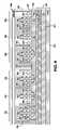
- FIG. 4is another cross-section of a portion of the memory array 32 illustrating a plurality of strings 82 of memory cells 84 in accordance with an embodiment of the present invention.
- each string 82may include any number of memory cells 84 .
- each memory cell 84may be formed from a control gate 56 and a floating gate 58 .
- Each string 82may include a source select gate transistor 86 and drain select gate transistor 88 .
- the memory cells 84 and select gates 86 and 88are disposed on a p-well 92 (p-type silicon) having n-doped regions 94 to form the source and drain regions for the memory cells 84 and the select gates 86 and 88 .
- the plurality of strings 82may include a plurality of common source contacts 96 and bitline contacts 98 .
- the p-well 92 and n-doped regions 94may couple to a bitline 100 for the memory cells 84 through the bitline contacts 98 , and a wordline (not shown) may be coupled to each control gate 56 . Additionally, the p-well 92 may be biased through the p-well contact 102 .
- the boosting plate 52is disposed in the SOI portion 54 such that the boosting plate 52 is disposed under the memory cells 84 of the strings 88 . Due to the disposition of the boosting plate 52 in the SOI portion 54 such that the p-well 92 and boosting plate 52 are separated by the SiO2 layer 64 , the boosting plate 52 is in capacitive contact with the p-well 92 . That is, biasing the boosting plate 52 may exert a capacitive coupling effect on the p-well 92 such that the p-well 92 may be influenced by the voltage on the boosting plate 52 .
- the p-well 92may couple up to a voltage if the boosting plate 52 is biased to a voltage. As explained further below, this capacitive coupling effect may be used to affect the p-well 92 during program and erase operations of the memory cells 84 . It should be appreciated that a boosting plate may be any size, shape, or topography suitable for achieving the desired capacitive coupling effect with the p-well 92
- FIG. 5depicts a block diagram of the SOI memory array 32 and drivers that may be used to operate the memory array 32 in accordance with an embodiment of the present invention.
- the memory array 32may be coupled to a wordline and select gate driver 104 and a bitline driver 106 to bias the wordlines and bitlines respectively during program, erase, read, and other operations.
- An array p-well driver 108may be coupled to the p-well contact 102
- an array source bias 110may be coupled to the common source contacts 96 .
- the boosting platemay be independently controlled through a boosting plate driver 112 coupled to the boosting plate 52 via the boosting plate contact 66 .
- FIG. 6Adepicts a schematic diagram of a portion of the memory array 32 in accordance with an embodiment of the present invention. Additionally, FIGS. 6B-6D depict p-well switching capability of the memory array 32 , which may be used to aid operation of the boosting plate 52 in accordance with another embodiment of the present invention.
- the memory array 32may include a plurality of strings 82 comprising a plurality of memory cells 84 .
- a string 82may include any number of memory cells 84 to store any number of units of data, such as any number of bits, bytes, etc.
- the NAND memory array 32includes local word lines WL( 0 )-WL(N) and intersecting local bit lines BL( 0 )-BL( 2 ).
- a connection 114 to a p-well 92 of the stringsis shown.
- a boosting plate connection 116is shown coupled to the p-well 92 , indicating the capacitive coupling effect of the boosting plate 52 .
- the NAND memory array 32includes the memory cells 84 located at each intersection of a local word line (WL) and a local bit line (BL).
- each memory cell 84includes a source, a drain, a floating gate, and a control gate.
- the control gate of each memory cell 84is coupled to (and in at least some cases form) a respective local word line (WL).
- the memory cells 84are connected in series, source to drain, to form the NAND string 82 formed between select gates. Specifically, the strings 82 are formed between the local drain select gates 88 and the source select gate 86 .
- a local drain select line (SGD)is coupled to a respective drain select gate 88 .
- the local source select lineis coupled to each NAND string 82 through the source select gate 86 .
- a “column” of the memory array 32includes a NAND string 82 and the source select gate 86 and drain select gate 88 connected thereto.
- a “row” of the memory cells 84are those transistors commonly coupled to a given local access line, such as a local word line (WL).
- cross-coupling effectsmay occur on adjacent memory cells.
- One such examplemay include a “program disturb” effect between memory cells of a programmed string (e.g., a string containing the memory cell or cells being programmed) and memory cells of an inhibited string (e.g., the string not being programmed).
- the program disturb effectmay be described with reference to FIG. 6 and a programmed string 120 and an inhibited string 122 .
- the wordline WL( 1 ) coupled to the memory cell 124may be biased to a program voltage (Vpgm).
- the wordlines WL( 0 ) and other wordlines in the programmed string 120may be biased to a pass voltage Vpass.
- the bitline BL( 0 ) coupled to the programmed string 120may be biased to 0V, and the bitline BL( 1 ) coupled to the inhibited string 122 may be floating or biased to Vcc.
- a memory cell 126 that is coupled to the wordline WL( 1 )may experience a program disturb, e.g., charge may become trapped in the floating gate of the memory cell 126 from the channel due to the voltage difference between the channel and the wordline WL( 1 ).
- the boosting plate 52may be biased to a certain voltage to influence the voltage of the p-well 92 ( FIG. 4 ) for both the programmed string 120 and inhibited string 122 .
- the memory array 32may include a p-well switch 125 coupled to a first p-well P-well( 0 ), a second p-well P-well( 1 ), and a third p-well P-well( 2 ) in accordance with an embodiment of the present invention.
- Each p-well P-well( 0 ), P-well( 1 ), and P-well( 2 )has individual p-well contacts 127 coupled to the p-well switch 125 .
- the p-well switch 125includes individual contacts 129 that each may be coupled to a voltage source, e.g., the p-well driver 108 or a node of the boosting plate 52 .
- the p-well switch 125enables each p-well to have individual voltages during operation of the memory array 32 .
- the p-well switch 125may be “OFF” such that each p-well P-well( 0 ), P-well( 1 ), and P-well( 2 ) are floating.
- the individual p-well contacts 127allow each p-well to have individual voltages.
- the p-well switchmay be “ON”, allowing the p-wells P-well( 0 ), P-well( 1 ), and P-well( 2 ) to be biased.
- the p-well switchmay “ON”, allowing the p-wells to be biased.
- each p-well node of P-well( 0 ), P-well( 1 ), and P-well( 2 )may be biased at common voltages through the p-well switch 125 .
- the P-well switch 125may be formed over the silicon 66 , similar to transistor array 68 .
- the p-well switch 125may be formed over the SOI portion 54 as part of the memory array 32 .
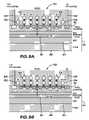
- FIGS. 7A and 7Bdepict a cross-section of the inhibited string 122 and programmed string 120 of the memory array 32 during programming of a memory cell in accordance with an embodiment of the present invention.
- the memory array 32is fabricated on the SOI portion 54 having the SiO2 layer 64 and silicon 66 .
- FIG. 7Adepicts a cross-section of the inhibited string 122 , e.g., those memory cells not being programmed and includes a common source contact 128 , a bitline contact 130 , and select gates 132 and 134 .
- FIG. 7Bdepicts a cross-section of the programmed string 120 , e.g., the string including those memory cells being programmed.
- FIG. 7Bincludes a common source contact 136 , a bitline contact 138 , and select gates 140 and 142 .
- the boosting plate 52may be biased to about 0V.
- the bitline coupled to bitline contact 130 of the inhibited string 122is biased to about 2V
- the bitline coupled to the bitline contact 138 of the programmed string 120is biased to about 0V.
- the source select gate 132 of the inhibited string 122 and the source select gate 140 of the programmed string 120may be biased to about 0V via the source gate select line (SGS).
- the drain select gates 134 and 142 of the inhibited string 122 and programmed string 120may be biased to about 2V via the drain select line (SGD).
- the p-well 92is floating and may experience minimal capacitive coupling effects from the boosting plate 52 .
- FIGS. 8A and 8Bdepict a cross-section of the inhibited string 122 and programmed string 120 during a second step of the programming operation in accordance with an embodiment of the present invention.
- the boosting plate 52may be biased to a voltage, Vboost.
- Vboostmay be about 10V.
- the bitline coupled to bitline contact 130 and the common source 128 of the inhibited string 122may be floating, enabling the p-well 92 to respond to the biased boosting plate 52 .
- the capacitive coupling effect between the boosting plate 52 and the p-well 92causes the p-well 92 to couple up to some voltage less than Vboost. For example, as shown in FIG. 8A , for a Vboost of about 10V, the p-well 92 may couple up to about 5V.
- the bitline coupled to bitline contact 138 of the programmed stringmay remain biased at about 0V.
- biasing of the boosting plate 52 to Vboostmay only minimally affect the p-well 92 .
- biasing the boosting plate 52 to about 10Vresults in a p-well voltage of about 0.5V in the programmed string 120 .
- FIGS. 9A and 9Bdepict a cross-section of the inhibited string 122 and programmed string 120 during a third program step in accordance with an operation of the present invention.
- the wordline (WL_sel) coupled to the memory cell 124may be biased to a program voltage, Vpgm, such as about 20V as shown in FIG. 9B .
- Vpgmprogram voltage
- the memory cell 126 of the inhibited string 122is also experiencing the voltage Vpgm of the wordline (WL_sel).
- the wordlines adjacent to the programmed memory cellmay be biased to a pass-through voltage (Vpass, also referred as an inhibited voltage Vinh), such as 10V, 5V, etc., as shown in FIGS. 9A and 9B .
- Vpassalso referred as an inhibited voltage Vinh
- the resulting difference in voltage between the p-well 92 of the inhibited string 122 (about 5V) and the p-well 92 of the programmed string 120 (about 0.5V)influences the behavior of the memory cells 124 and 126 coupled to the selected wordline.
- the voltage difference between the selected wordline and the channel on the p-well 92may be low enough to minimize or eliminate any program disturb.
- the difference in voltagemay minimize or eliminate any flow of charge from the channel into the floating gate of the memory cell 126 .
- the voltage difference between the selected wordline and the boosted p-well 92may be large enough to allow normal programming of the memory cell 124 .
- the floated p-well voltage of the programmed stringmay about 0.5V
- the selected wordlinemay be biased to a Vpgm of about 20V, thus allowing charge from the channel to become trapped in the floating gate of the programmed memory cell 124 .
- the boosting plate 52may affect the p-well such that the p-well of both an inhibited string and a programmed string is optimized to reduce or eliminate program disturb and allow programming of any memory cells of the programmed string.
- the boosting plate 52may be used during an erase operation of a block of memory cells of the memory array 32 .
- the p-well 92is biased to an erase voltage Verase, such that charge flows out of the floating gate of the erased memory cells.
- Veraseerase voltage
- the boosting plate 52may be used to reduce this RC delay of the p-well 92 and reduce the time for execution of the erase operation.
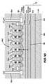
- FIG. 10depicts a cross section of a string 150 of the memory array 32 during an erase in accordance with an embodiment of the present invention.
- the string 150is fabricated on the SOI portion 54 having the SiO2 layer 64 and silicon substrate 66 .
- the stringincludes a common source contact 152 , a bitline contact 154 , select gates 156 and 158 , and memory cells 160 .
- the wordlines of the erased stringmay be biased to an erase voltage Vw 1 .
- the source select gate 156 , drain select gate 158 , common source coupled to common contact 152 and bitline coupled to bitline contact 154 of the erased stringare floating.
- the boosting plate 52may be biased to an erase voltage (Verase).
- Veraseerase voltage
- the p-well 92is also biased to Verase (such as by turning on the p-well switch 125 )
- biasing the boosting plate before the eraseallows the capacitive coupling effect between the boosting plate 52 and p-well 92 to aid coupling the p-well 92 to Verase.
- the boosting plate 52may be biased to any suitable voltage to capacitive couple the p-well to the desired erase voltage (Verase), such as about 10V.
- Verasedesired erase voltage
- Table 2the voltages applied to the lines, p-well 92 , and boosting plate 52 of the erased string are summarized below in Table 2:
- the boosting plate 52may be grounded to eliminate any effect of the boosting plate 52 on the p-well 92 .
- Table 3the voltages applied to the lines, p-well, and boosting plate of are summarized below in Table 3:
Landscapes
- Read Only Memory (AREA)
- Semiconductor Memories (AREA)
- Non-Volatile Memory (AREA)
Abstract
Description
| TABLE 1 | ||
| Pgm | ||
| WL_sel | Vpgm | ||
| WL_unsel | Vpass (Vinh) | ||
| SGS | Vsgs | ||
| SGD | Vsgd | ||
| BL_sel | Vbl_sel | ||
| BL_unsel | Vbl_unsel -> floating | ||
| Common source | Vsource -> floating | ||
| P-well | Floating | ||
| Boosting plate | Vboost | ||
| P-well switch | OFF | ||
| TABLE 2 | ||
| Erase | ||
| WL | Vwl | ||
| BL | Floating | ||
| SGS | Floating | ||
| SGD | Floating | ||
| Common source | Floating | ||
| P-well | |||
| Boosting plate | |||
| 10 V or Verase | |||
| P-well switch | ON | ||
| TABLE 3 | ||
| Read | ||
| WL_sel | Vref | ||
| WL_unsel | Vread | ||
| SGS | Vsgs | ||
| SGD | Vsgd | ||
| BL_sel | Vbl_sel | ||
| BL_unsel | 0 V | ||
| Common source | GND | ||
| P-well | GND | ||
| Boosting plate | GND | ||
| P-well switch | ON | ||
Claims (12)
Priority Applications (3)
| Application Number | Priority Date | Filing Date | Title |
|---|---|---|---|
| US12/402,300US8098529B2 (en) | 2009-03-11 | 2009-03-11 | Memory device having buried boosting plate and methods of operating the same |
| US13/351,148US8634252B2 (en) | 2009-03-11 | 2012-01-16 | Methods of operating a memory device having a buried boosting plate |
| US14/159,198US9281073B2 (en) | 2009-03-11 | 2014-01-20 | Methods of operating a memory device having a buried boosting plate |
Applications Claiming Priority (1)
| Application Number | Priority Date | Filing Date | Title |
|---|---|---|---|
| US12/402,300US8098529B2 (en) | 2009-03-11 | 2009-03-11 | Memory device having buried boosting plate and methods of operating the same |
Related Child Applications (1)
| Application Number | Title | Priority Date | Filing Date |
|---|---|---|---|
| US13/351,148DivisionUS8634252B2 (en) | 2009-03-11 | 2012-01-16 | Methods of operating a memory device having a buried boosting plate |
Publications (2)
| Publication Number | Publication Date |
|---|---|
| US20100232235A1 US20100232235A1 (en) | 2010-09-16 |
| US8098529B2true US8098529B2 (en) | 2012-01-17 |
Family
ID=42730600
Family Applications (2)
| Application Number | Title | Priority Date | Filing Date |
|---|---|---|---|
| US12/402,300Active2029-06-13US8098529B2 (en) | 2009-03-11 | 2009-03-11 | Memory device having buried boosting plate and methods of operating the same |
| US13/351,148ActiveUS8634252B2 (en) | 2009-03-11 | 2012-01-16 | Methods of operating a memory device having a buried boosting plate |
Family Applications After (1)
| Application Number | Title | Priority Date | Filing Date |
|---|---|---|---|
| US13/351,148ActiveUS8634252B2 (en) | 2009-03-11 | 2012-01-16 | Methods of operating a memory device having a buried boosting plate |
Country Status (1)
| Country | Link |
|---|---|
| US (2) | US8098529B2 (en) |
Cited By (3)
| Publication number | Priority date | Publication date | Assignee | Title |
|---|---|---|---|---|
| US20130056826A1 (en)* | 2011-09-01 | 2013-03-07 | Taiwan Semiconductor Manufacturing Company, Ltd. | Multi-Fin Device and Method of Making Same |
| US20150206592A1 (en)* | 2009-03-11 | 2015-07-23 | Micron Technology, Inc. | Methods of operating a memory device having a buried boosting plate |
| US9171626B2 (en) | 2012-07-30 | 2015-10-27 | Micron Technology, Inc.. | Memory devices and programming memory arrays thereof |
Families Citing this family (4)
| Publication number | Priority date | Publication date | Assignee | Title |
|---|---|---|---|---|
| US20080273389A1 (en)* | 2007-03-21 | 2008-11-06 | Micron Technology, Inc. | Flash memory cells, NAND cell units, methods of forming NAND cell units, and methods of programming NAND cell unit strings |
| KR101702356B1 (en)* | 2010-08-09 | 2017-02-03 | 삼성전자주식회사 | Charge trap flash memory device and erasing method thereof |
| US8648414B2 (en) | 2011-07-01 | 2014-02-11 | Micron Technology, Inc. | Semiconductor structures including bodies of semiconductor material, devices including such structures and related methods |
| JP2019096756A (en)* | 2017-11-24 | 2019-06-20 | セイコーエプソン株式会社 | Writing method for semiconductor storage device |
Citations (17)
| Publication number | Priority date | Publication date | Assignee | Title |
|---|---|---|---|---|
| US5600588A (en)* | 1994-01-24 | 1997-02-04 | Fujitsu Limited | Data retention circuit and semiconductor memory device using the same |
| US5610533A (en)* | 1993-11-29 | 1997-03-11 | Mitsubishi Denki Kabushiki Kaisha | Switched substrate bias for logic circuits |
| US6061267A (en)* | 1998-09-28 | 2000-05-09 | Texas Instruments Incorporated | Memory circuits, systems, and methods with cells using back bias to control the threshold voltage of one or more corresponding cell transistors |
| US6115287A (en) | 1997-11-27 | 2000-09-05 | Kabushiki Kaisha Toshiba | Nonvolatile semiconductor memory device using SOI |
| US20040099878A1 (en)* | 2002-11-26 | 2004-05-27 | Motorola, Inc. | Structure to reduce signal cross-talk through semiconductor substrate for system on chip applications |
| US20060278927A1 (en) | 2005-06-11 | 2006-12-14 | Seoul National University Industry Foundation | Body biasing structure of soi |
| US20070047314A1 (en) | 2005-08-31 | 2007-03-01 | Micron Technology, Inc. | Programming method for NAND EEPROM |
| US20070047327A1 (en) | 2005-08-31 | 2007-03-01 | Micron Technology, Inc. | Erase method for flash memory |
| US20070052011A1 (en)* | 2005-08-24 | 2007-03-08 | Micron Technology, Inc. | Scalable multi-functional and multi-level nano-crystal non-volatile memory device |
| US20070241369A1 (en) | 2006-04-18 | 2007-10-18 | Micron Technology, Inc. | Couplings within memory devices and methods |
| US20070247908A1 (en) | 2006-04-19 | 2007-10-25 | Micron Techonology, Inc. | Read operation for NAND memory |
| US20080037307A1 (en) | 2006-08-09 | 2008-02-14 | Micron Technology, Inc. | Non-volatile memory erase verify |
| US20080049494A1 (en) | 2006-08-22 | 2008-02-28 | Micron Technology, Inc. | Reducing effects of program disturb in a memory device |
| US20080175060A1 (en)* | 2007-01-24 | 2008-07-24 | Kilopass Technology, Inc. | Non-volatile semiconductor memory based on enhanced gate oxide breakdown |
| US7408811B2 (en) | 2005-05-02 | 2008-08-05 | Kabushiki Kaisha Toshiba | NAND-type flash memory on an SOI substrate with a carrier discharging operation |
| US20080273385A1 (en) | 2007-05-03 | 2008-11-06 | Micron Technology, Inc. | NAND step up voltage switching method |
| US20090001442A1 (en)* | 2007-06-26 | 2009-01-01 | Yoshio Ozawa | Nonvolatile semiconductor memory device and method of manufacturing the same |
Family Cites Families (4)
| Publication number | Priority date | Publication date | Assignee | Title |
|---|---|---|---|---|
| US20050179111A1 (en)* | 2004-02-12 | 2005-08-18 | Iwen Chao | Semiconductor device with low resistive path barrier |
| US7885119B2 (en)* | 2006-07-20 | 2011-02-08 | Sandisk Corporation | Compensating for coupling during programming |
| US7869273B2 (en)* | 2007-09-04 | 2011-01-11 | Sandisk Corporation | Reducing the impact of interference during programming |
| US7961514B2 (en)* | 2009-01-07 | 2011-06-14 | Infineon Technologies Ag | Semiconductor device, a method of using a semiconductor device, a programmable memory device, and method of producing a semiconductor device |
- 2009
- 2009-03-11USUS12/402,300patent/US8098529B2/enactiveActive
- 2012
- 2012-01-16USUS13/351,148patent/US8634252B2/enactiveActive
Patent Citations (20)
| Publication number | Priority date | Publication date | Assignee | Title |
|---|---|---|---|---|
| US5610533A (en)* | 1993-11-29 | 1997-03-11 | Mitsubishi Denki Kabushiki Kaisha | Switched substrate bias for logic circuits |
| US5600588A (en)* | 1994-01-24 | 1997-02-04 | Fujitsu Limited | Data retention circuit and semiconductor memory device using the same |
| US6115287A (en) | 1997-11-27 | 2000-09-05 | Kabushiki Kaisha Toshiba | Nonvolatile semiconductor memory device using SOI |
| US6061267A (en)* | 1998-09-28 | 2000-05-09 | Texas Instruments Incorporated | Memory circuits, systems, and methods with cells using back bias to control the threshold voltage of one or more corresponding cell transistors |
| US20040099878A1 (en)* | 2002-11-26 | 2004-05-27 | Motorola, Inc. | Structure to reduce signal cross-talk through semiconductor substrate for system on chip applications |
| US7408811B2 (en) | 2005-05-02 | 2008-08-05 | Kabushiki Kaisha Toshiba | NAND-type flash memory on an SOI substrate with a carrier discharging operation |
| US20060278927A1 (en) | 2005-06-11 | 2006-12-14 | Seoul National University Industry Foundation | Body biasing structure of soi |
| US20070052011A1 (en)* | 2005-08-24 | 2007-03-08 | Micron Technology, Inc. | Scalable multi-functional and multi-level nano-crystal non-volatile memory device |
| US20070047314A1 (en) | 2005-08-31 | 2007-03-01 | Micron Technology, Inc. | Programming method for NAND EEPROM |
| US20070047327A1 (en) | 2005-08-31 | 2007-03-01 | Micron Technology, Inc. | Erase method for flash memory |
| US7292476B2 (en) | 2005-08-31 | 2007-11-06 | Micron Technology, Inc. | Programming method for NAND EEPROM |
| US20080008006A1 (en) | 2005-08-31 | 2008-01-10 | Micron Technology, Inc. | Programming method for NAND EEPROM |
| US7499330B2 (en) | 2005-08-31 | 2009-03-03 | Micron Technology, Inc. | Programming method for NAND EEPROM |
| US20070241369A1 (en) | 2006-04-18 | 2007-10-18 | Micron Technology, Inc. | Couplings within memory devices and methods |
| US20070247908A1 (en) | 2006-04-19 | 2007-10-25 | Micron Techonology, Inc. | Read operation for NAND memory |
| US20080037307A1 (en) | 2006-08-09 | 2008-02-14 | Micron Technology, Inc. | Non-volatile memory erase verify |
| US20080049494A1 (en) | 2006-08-22 | 2008-02-28 | Micron Technology, Inc. | Reducing effects of program disturb in a memory device |
| US20080175060A1 (en)* | 2007-01-24 | 2008-07-24 | Kilopass Technology, Inc. | Non-volatile semiconductor memory based on enhanced gate oxide breakdown |
| US20080273385A1 (en) | 2007-05-03 | 2008-11-06 | Micron Technology, Inc. | NAND step up voltage switching method |
| US20090001442A1 (en)* | 2007-06-26 | 2009-01-01 | Yoshio Ozawa | Nonvolatile semiconductor memory device and method of manufacturing the same |
Non-Patent Citations (1)
| Title |
|---|
| Park, Han II et al., "Depletion-Enhanced Body-Isolation (DEBI) Array on SOI for Highly Scalable and Reliable NAND Flash Memories", IEEE Transactions, vol. 5, Issue 3, pp. 201-204, May 2006. |
Cited By (10)
| Publication number | Priority date | Publication date | Assignee | Title |
|---|---|---|---|---|
| US20150206592A1 (en)* | 2009-03-11 | 2015-07-23 | Micron Technology, Inc. | Methods of operating a memory device having a buried boosting plate |
| US9281073B2 (en)* | 2009-03-11 | 2016-03-08 | Micron Technology, Inc. | Methods of operating a memory device having a buried boosting plate |
| US20130056826A1 (en)* | 2011-09-01 | 2013-03-07 | Taiwan Semiconductor Manufacturing Company, Ltd. | Multi-Fin Device and Method of Making Same |
| US9287385B2 (en)* | 2011-09-01 | 2016-03-15 | Taiwan Semiconductor Manufacturing Company, Ltd. | Multi-fin device and method of making same |
| US9312363B2 (en) | 2011-09-01 | 2016-04-12 | Taiwan Semiconductor Manufacturing Company, Ltd. | Multi-fin device and method of making same |
| US9893061B2 (en) | 2011-09-01 | 2018-02-13 | Taiwan Semiconductor Manufacturing Company, Ltd. | Multi-Fin device and method of making same |
| US10157920B2 (en) | 2011-09-01 | 2018-12-18 | Taiwan Semiconductor Manufacturing Company, Ltd. | Multi-fin device and method of making same |
| US10679990B2 (en) | 2011-09-01 | 2020-06-09 | Taiwan Semiconductor Manufacturing Company, Ltd. | Multi-fin device and method of making same |
| US9171626B2 (en) | 2012-07-30 | 2015-10-27 | Micron Technology, Inc.. | Memory devices and programming memory arrays thereof |
| US9437304B2 (en) | 2012-07-30 | 2016-09-06 | Micron Technology, Inc. | Memory devices and programming memory arrays thereof |
Also Published As
| Publication number | Publication date |
|---|---|
| US20100232235A1 (en) | 2010-09-16 |
| US8634252B2 (en) | 2014-01-21 |
| US20120113713A1 (en) | 2012-05-10 |
Similar Documents
| Publication | Publication Date | Title |
|---|---|---|
| US9030874B2 (en) | Adjusting program and erase voltages in a memory device | |
| US9019766B2 (en) | Biasing system and method | |
| US7570517B2 (en) | Flash memory device adapted to prevent read failures due to dummy strings | |
| US8634252B2 (en) | Methods of operating a memory device having a buried boosting plate | |
| US7403429B2 (en) | Method of erasing data with improving reliability in a nonvolatile semiconductor memory device | |
| US8325522B2 (en) | Memory array of floating gate-based non-volatile memory cells | |
| KR100553631B1 (en) | Nonvolatile semiconductor memory | |
| US20150001608A1 (en) | Simple and cost-free mtp structure | |
| US7554846B2 (en) | Select gate transistors and methods of operating the same | |
| US7952936B2 (en) | Program-verify method | |
| JP5130571B2 (en) | Semiconductor device | |
| US9281073B2 (en) | Methods of operating a memory device having a buried boosting plate | |
| US20090003065A1 (en) | Flash cell with improved program disturb | |
| JPH07249293A (en) | Low-voltage flash eeprom memory cell | |
| JP2006005371A (en) | Nonvolatile semiconductor memory device | |
| JP3577290B2 (en) | Nonvolatile semiconductor memory device | |
| US7675778B2 (en) | Memory devices having reduced word line current and method of operating and manufacturing the same | |
| KR20140086566A (en) | Non-volatile memory device | |
| JP2001358238A (en) | Nonvolatile semiconductor memory device | |
| JP2006005372A (en) | Nonvolatile semiconductor memory device |
Legal Events
| Date | Code | Title | Description |
|---|---|---|---|
| AS | Assignment | Owner name:MICRON TECHNOLOGY, INC., IDAHO Free format text:ASSIGNMENT OF ASSIGNORS INTEREST;ASSIGNOR:GODA, AKIRA;REEL/FRAME:022379/0359 Effective date:20090310 | |
| FEPP | Fee payment procedure | Free format text:PAYOR NUMBER ASSIGNED (ORIGINAL EVENT CODE: ASPN); ENTITY STATUS OF PATENT OWNER: LARGE ENTITY | |
| STCF | Information on status: patent grant | Free format text:PATENTED CASE | |
| FPAY | Fee payment | Year of fee payment:4 | |
| AS | Assignment | Owner name:U.S. BANK NATIONAL ASSOCIATION, AS COLLATERAL AGENT, CALIFORNIA Free format text:SECURITY INTEREST;ASSIGNOR:MICRON TECHNOLOGY, INC.;REEL/FRAME:038669/0001 Effective date:20160426 Owner name:U.S. BANK NATIONAL ASSOCIATION, AS COLLATERAL AGEN Free format text:SECURITY INTEREST;ASSIGNOR:MICRON TECHNOLOGY, INC.;REEL/FRAME:038669/0001 Effective date:20160426 | |
| AS | Assignment | Owner name:MORGAN STANLEY SENIOR FUNDING, INC., AS COLLATERAL AGENT, MARYLAND Free format text:PATENT SECURITY AGREEMENT;ASSIGNOR:MICRON TECHNOLOGY, INC.;REEL/FRAME:038954/0001 Effective date:20160426 Owner name:MORGAN STANLEY SENIOR FUNDING, INC., AS COLLATERAL Free format text:PATENT SECURITY AGREEMENT;ASSIGNOR:MICRON TECHNOLOGY, INC.;REEL/FRAME:038954/0001 Effective date:20160426 | |
| AS | Assignment | Owner name:U.S. BANK NATIONAL ASSOCIATION, AS COLLATERAL AGENT, CALIFORNIA Free format text:CORRECTIVE ASSIGNMENT TO CORRECT THE REPLACE ERRONEOUSLY FILED PATENT #7358718 WITH THE CORRECT PATENT #7358178 PREVIOUSLY RECORDED ON REEL 038669 FRAME 0001. ASSIGNOR(S) HEREBY CONFIRMS THE SECURITY INTEREST;ASSIGNOR:MICRON TECHNOLOGY, INC.;REEL/FRAME:043079/0001 Effective date:20160426 Owner name:U.S. BANK NATIONAL ASSOCIATION, AS COLLATERAL AGEN Free format text:CORRECTIVE ASSIGNMENT TO CORRECT THE REPLACE ERRONEOUSLY FILED PATENT #7358718 WITH THE CORRECT PATENT #7358178 PREVIOUSLY RECORDED ON REEL 038669 FRAME 0001. ASSIGNOR(S) HEREBY CONFIRMS THE SECURITY INTEREST;ASSIGNOR:MICRON TECHNOLOGY, INC.;REEL/FRAME:043079/0001 Effective date:20160426 | |
| AS | Assignment | Owner name:JPMORGAN CHASE BANK, N.A., AS COLLATERAL AGENT, ILLINOIS Free format text:SECURITY INTEREST;ASSIGNORS:MICRON TECHNOLOGY, INC.;MICRON SEMICONDUCTOR PRODUCTS, INC.;REEL/FRAME:047540/0001 Effective date:20180703 Owner name:JPMORGAN CHASE BANK, N.A., AS COLLATERAL AGENT, IL Free format text:SECURITY INTEREST;ASSIGNORS:MICRON TECHNOLOGY, INC.;MICRON SEMICONDUCTOR PRODUCTS, INC.;REEL/FRAME:047540/0001 Effective date:20180703 | |
| AS | Assignment | Owner name:MICRON TECHNOLOGY, INC., IDAHO Free format text:RELEASE BY SECURED PARTY;ASSIGNOR:U.S. BANK NATIONAL ASSOCIATION, AS COLLATERAL AGENT;REEL/FRAME:047243/0001 Effective date:20180629 | |
| MAFP | Maintenance fee payment | Free format text:PAYMENT OF MAINTENANCE FEE, 8TH YEAR, LARGE ENTITY (ORIGINAL EVENT CODE: M1552); ENTITY STATUS OF PATENT OWNER: LARGE ENTITY Year of fee payment:8 | |
| AS | Assignment | Owner name:MICRON TECHNOLOGY, INC., IDAHO Free format text:RELEASE BY SECURED PARTY;ASSIGNOR:MORGAN STANLEY SENIOR FUNDING, INC., AS COLLATERAL AGENT;REEL/FRAME:050937/0001 Effective date:20190731 | |
| AS | Assignment | Owner name:MICRON TECHNOLOGY, INC., IDAHO Free format text:RELEASE BY SECURED PARTY;ASSIGNOR:JPMORGAN CHASE BANK, N.A., AS COLLATERAL AGENT;REEL/FRAME:051028/0001 Effective date:20190731 Owner name:MICRON SEMICONDUCTOR PRODUCTS, INC., IDAHO Free format text:RELEASE BY SECURED PARTY;ASSIGNOR:JPMORGAN CHASE BANK, N.A., AS COLLATERAL AGENT;REEL/FRAME:051028/0001 Effective date:20190731 | |
| MAFP | Maintenance fee payment | Free format text:PAYMENT OF MAINTENANCE FEE, 12TH YEAR, LARGE ENTITY (ORIGINAL EVENT CODE: M1553); ENTITY STATUS OF PATENT OWNER: LARGE ENTITY Year of fee payment:12 |