US8094984B2 - Semiconductor constructions, methods of forming semiconductor constructions, light-conducting conduits, and optical signal propagation assemblies - Google Patents
Semiconductor constructions, methods of forming semiconductor constructions, light-conducting conduits, and optical signal propagation assembliesDownload PDFInfo
- Publication number
- US8094984B2 US8094984B2US12/849,132US84913210AUS8094984B2US 8094984 B2US8094984 B2US 8094984B2US 84913210 AUS84913210 AUS 84913210AUS 8094984 B2US8094984 B2US 8094984B2
- Authority
- US
- United States
- Prior art keywords
- segment
- rare earth
- sheath
- earth elements
- light
- Prior art date
- Legal status (The legal status is an assumption and is not a legal conclusion. Google has not performed a legal analysis and makes no representation as to the accuracy of the status listed.)
- Active
Links
- 230000003287optical effectEffects0.000titleclaimsabstractdescription96
- 238000010276constructionMethods0.000titleclaimsabstractdescription26
- 239000004065semiconductorSubstances0.000titleclaimsabstractdescription25
- 238000000034methodMethods0.000titleabstractdescription14
- 230000000712assemblyEffects0.000titledescription4
- 238000000429assemblyMethods0.000titledescription4
- 239000000463materialSubstances0.000claimsabstractdescription119
- 229910052761rare earth metalInorganic materials0.000claimsabstractdescription77
- 239000011159matrix materialSubstances0.000claimsabstractdescription22
- 229910052691ErbiumInorganic materials0.000claimsabstractdescription18
- UYAHIZSMUZPPFV-UHFFFAOYSA-NerbiumChemical compound[Er]UYAHIZSMUZPPFV-UHFFFAOYSA-N0.000claimsabstractdescription17
- 239000000758substrateSubstances0.000claimsdescription44
- VYPSYNLAJGMNEJ-UHFFFAOYSA-NSilicium dioxideChemical compoundO=[Si]=OVYPSYNLAJGMNEJ-UHFFFAOYSA-N0.000claimsdescription39
- 239000000203mixtureSubstances0.000claimsdescription28
- 235000012239silicon dioxideNutrition0.000claimsdescription18
- 239000000377silicon dioxideSubstances0.000claimsdescription18
- AMGQUBHHOARCQH-UHFFFAOYSA-Nindium;oxotinChemical compound[In].[Sn]=OAMGQUBHHOARCQH-UHFFFAOYSA-N0.000claimsdescription15
- KYKLWYKWCAYAJY-UHFFFAOYSA-Noxotin;zincChemical compound[Zn].[Sn]=OKYKLWYKWCAYAJY-UHFFFAOYSA-N0.000claimsdescription15
- 229910052581Si3N4Inorganic materials0.000claimsdescription9
- HQVNEWCFYHHQES-UHFFFAOYSA-Nsilicon nitrideChemical compoundN12[Si]34N5[Si]62N3[Si]51N64HQVNEWCFYHHQES-UHFFFAOYSA-N0.000claimsdescription9
- 238000011144upstream manufacturingMethods0.000claimsdescription5
- 230000004888barrier functionEffects0.000abstractdescription25
- XUIMIQQOPSSXEZ-UHFFFAOYSA-NSiliconChemical compound[Si]XUIMIQQOPSSXEZ-UHFFFAOYSA-N0.000abstractdescription11
- 229910052710siliconInorganic materials0.000abstractdescription11
- 239000010703siliconSubstances0.000abstractdescription11
- 239000007769metal materialSubstances0.000abstractdescription9
- 239000002159nanocrystalSubstances0.000abstractdescription8
- 229910052684CeriumInorganic materials0.000abstractdescription6
- 239000003989dielectric materialSubstances0.000abstractdescription6
- GWXLDORMOJMVQZ-UHFFFAOYSA-NceriumChemical compound[Ce]GWXLDORMOJMVQZ-UHFFFAOYSA-N0.000abstract1
- 238000012545processingMethods0.000description11
- 239000012634fragmentSubstances0.000description7
- 238000010348incorporationMethods0.000description6
- ZMIGMASIKSOYAM-UHFFFAOYSA-NceriumChemical compound[Ce][Ce][Ce][Ce][Ce][Ce][Ce][Ce][Ce][Ce][Ce][Ce][Ce][Ce][Ce][Ce][Ce][Ce][Ce][Ce][Ce][Ce][Ce][Ce][Ce][Ce][Ce][Ce][Ce][Ce][Ce][Ce][Ce][Ce][Ce][Ce][Ce][Ce]ZMIGMASIKSOYAM-UHFFFAOYSA-N0.000description5
- 229910052779NeodymiumInorganic materials0.000description4
- 229910052769YtterbiumInorganic materials0.000description4
- 238000005516engineering processMethods0.000description4
- 229910021421monocrystalline siliconInorganic materials0.000description4
- QEFYFXOXNSNQGX-UHFFFAOYSA-Nneodymium atomChemical compound[Nd]QEFYFXOXNSNQGX-UHFFFAOYSA-N0.000description4
- 238000012546transferMethods0.000description4
- NAWDYIZEMPQZHO-UHFFFAOYSA-NytterbiumChemical compound[Yb]NAWDYIZEMPQZHO-UHFFFAOYSA-N0.000description4
- 239000002019doping agentSubstances0.000description3
- 239000011521glassSubstances0.000description3
- 238000002513implantationMethods0.000description3
- 238000004519manufacturing processMethods0.000description3
- 229910052814silicon oxideInorganic materials0.000description3
- -1Erbium ionsChemical class0.000description2
- 239000003929acidic solutionSubstances0.000description2
- 230000003321amplificationEffects0.000description2
- 239000005380borophosphosilicate glassSubstances0.000description2
- 239000000969carrierSubstances0.000description2
- 229910000420cerium oxideInorganic materials0.000description2
- 230000000694effectsEffects0.000description2
- 230000005284excitationEffects0.000description2
- 229910052751metalInorganic materials0.000description2
- 239000002184metalSubstances0.000description2
- 238000003199nucleic acid amplification methodMethods0.000description2
- BMMGVYCKOGBVEV-UHFFFAOYSA-Noxo(oxoceriooxy)ceriumChemical compound[Ce]=O.O=[Ce]=OBMMGVYCKOGBVEV-UHFFFAOYSA-N0.000description2
- 230000037361pathwayEffects0.000description2
- 239000005360phosphosilicate glassSubstances0.000description2
- 230000000704physical effectEffects0.000description2
- 230000005855radiationEffects0.000description2
- ZOXJGFHDIHLPTG-UHFFFAOYSA-NBoronChemical compound[B]ZOXJGFHDIHLPTG-UHFFFAOYSA-N0.000description1
- VEXZGXHMUGYJMC-UHFFFAOYSA-MChloride anionChemical compound[Cl-]VEXZGXHMUGYJMC-UHFFFAOYSA-M0.000description1
- RYGMFSIKBFXOCR-UHFFFAOYSA-NCopperChemical compound[Cu]RYGMFSIKBFXOCR-UHFFFAOYSA-N0.000description1
- 229910052692DysprosiumInorganic materials0.000description1
- 229910052693EuropiumInorganic materials0.000description1
- PXGOKWXKJXAPGV-UHFFFAOYSA-NFluorineChemical compoundFFPXGOKWXKJXAPGV-UHFFFAOYSA-N0.000description1
- 229910052688GadoliniumInorganic materials0.000description1
- 229910052689HolmiumInorganic materials0.000description1
- VEXZGXHMUGYJMC-UHFFFAOYSA-NHydrochloric acidChemical compoundClVEXZGXHMUGYJMC-UHFFFAOYSA-N0.000description1
- 229910052765LutetiumInorganic materials0.000description1
- OAICVXFJPJFONN-UHFFFAOYSA-NPhosphorusChemical compound[P]OAICVXFJPJFONN-UHFFFAOYSA-N0.000description1
- 229910052777PraseodymiumInorganic materials0.000description1
- 229910052773PromethiumInorganic materials0.000description1
- 229910052772SamariumInorganic materials0.000description1
- 229910052771TerbiumInorganic materials0.000description1
- 229910052775ThuliumInorganic materials0.000description1
- 229910052782aluminiumInorganic materials0.000description1
- XAGFODPZIPBFFR-UHFFFAOYSA-NaluminiumChemical compound[Al]XAGFODPZIPBFFR-UHFFFAOYSA-N0.000description1
- 230000009286beneficial effectEffects0.000description1
- 229910052796boronInorganic materials0.000description1
- 150000001805chlorine compoundsChemical class0.000description1
- 150000001875compoundsChemical class0.000description1
- 229910052802copperInorganic materials0.000description1
- 239000010949copperSubstances0.000description1
- 239000012895dilutionSubstances0.000description1
- 238000010790dilutionMethods0.000description1
- KBQHZAAAGSGFKK-UHFFFAOYSA-Ndysprosium atomChemical compound[Dy]KBQHZAAAGSGFKK-UHFFFAOYSA-N0.000description1
- ZXGIFJXRQHZCGJ-UHFFFAOYSA-Nerbium(3+);oxygen(2-)Chemical compound[O-2].[O-2].[O-2].[Er+3].[Er+3]ZXGIFJXRQHZCGJ-UHFFFAOYSA-N0.000description1
- HDGGAKOVUDZYES-UHFFFAOYSA-Kerbium(iii) chlorideChemical compoundCl[Er](Cl)ClHDGGAKOVUDZYES-UHFFFAOYSA-K0.000description1
- OGPBJKLSAFTDLK-UHFFFAOYSA-Neuropium atomChemical compound[Eu]OGPBJKLSAFTDLK-UHFFFAOYSA-N0.000description1
- 239000000835fiberSubstances0.000description1
- 229910052731fluorineInorganic materials0.000description1
- 239000011737fluorineSubstances0.000description1
- 229940104869fluorosilicateDrugs0.000description1
- UIWYJDYFSGRHKR-UHFFFAOYSA-Ngadolinium atomChemical compound[Gd]UIWYJDYFSGRHKR-UHFFFAOYSA-N0.000description1
- KJZYNXUDTRRSPN-UHFFFAOYSA-Nholmium atomChemical compound[Ho]KJZYNXUDTRRSPN-UHFFFAOYSA-N0.000description1
- 239000007943implantSubstances0.000description1
- OHSVLFRHMCKCQY-UHFFFAOYSA-Nlutetium atomChemical compound[Lu]OHSVLFRHMCKCQY-UHFFFAOYSA-N0.000description1
- 230000007246mechanismEffects0.000description1
- 238000012986modificationMethods0.000description1
- 230000004048modificationEffects0.000description1
- 229910052698phosphorusInorganic materials0.000description1
- 239000011574phosphorusSubstances0.000description1
- 238000005498polishingMethods0.000description1
- PUDIUYLPXJFUGB-UHFFFAOYSA-Npraseodymium atomChemical compound[Pr]PUDIUYLPXJFUGB-UHFFFAOYSA-N0.000description1
- 230000008569processEffects0.000description1
- VQMWBBYLQSCNPO-UHFFFAOYSA-Npromethium atomChemical compound[Pm]VQMWBBYLQSCNPO-UHFFFAOYSA-N0.000description1
- 238000009877renderingMethods0.000description1
- KZUNJOHGWZRPMI-UHFFFAOYSA-Nsamarium atomChemical compound[Sm]KZUNJOHGWZRPMI-UHFFFAOYSA-N0.000description1
- 229910021332silicideInorganic materials0.000description1
- 239000007787solidSubstances0.000description1
- 239000000243solutionSubstances0.000description1
- GZCRRIHWUXGPOV-UHFFFAOYSA-Nterbium atomChemical compound[Tb]GZCRRIHWUXGPOV-UHFFFAOYSA-N0.000description1
- 229910021341titanium silicideInorganic materials0.000description1
- WFKWXMTUELFFGS-UHFFFAOYSA-NtungstenChemical compound[W]WFKWXMTUELFFGS-UHFFFAOYSA-N0.000description1
- 229910052721tungstenInorganic materials0.000description1
- 239000010937tungstenSubstances0.000description1
- WQJQOUPTWCFRMM-UHFFFAOYSA-Ntungsten disilicideChemical compound[Si]#[W]#[Si]WQJQOUPTWCFRMM-UHFFFAOYSA-N0.000description1
- 229910021342tungsten silicideInorganic materials0.000description1
- XLYOFNOQVPJJNP-UHFFFAOYSA-NwaterSubstancesOXLYOFNOQVPJJNP-UHFFFAOYSA-N0.000description1
Images


Classifications
- G—PHYSICS
- G02—OPTICS
- G02B—OPTICAL ELEMENTS, SYSTEMS OR APPARATUS
- G02B6/00—Light guides; Structural details of arrangements comprising light guides and other optical elements, e.g. couplings
- G02B6/10—Light guides; Structural details of arrangements comprising light guides and other optical elements, e.g. couplings of the optical waveguide type
- G02B6/12—Light guides; Structural details of arrangements comprising light guides and other optical elements, e.g. couplings of the optical waveguide type of the integrated circuit kind
- G—PHYSICS
- G02—OPTICS
- G02B—OPTICAL ELEMENTS, SYSTEMS OR APPARATUS
- G02B6/00—Light guides; Structural details of arrangements comprising light guides and other optical elements, e.g. couplings
- G02B6/10—Light guides; Structural details of arrangements comprising light guides and other optical elements, e.g. couplings of the optical waveguide type
- H—ELECTRICITY
- H01—ELECTRIC ELEMENTS
- H01S—DEVICES USING THE PROCESS OF LIGHT AMPLIFICATION BY STIMULATED EMISSION OF RADIATION [LASER] TO AMPLIFY OR GENERATE LIGHT; DEVICES USING STIMULATED EMISSION OF ELECTROMAGNETIC RADIATION IN WAVE RANGES OTHER THAN OPTICAL
- H01S3/00—Lasers, i.e. devices using stimulated emission of electromagnetic radiation in the infrared, visible or ultraviolet wave range
- H01S3/05—Construction or shape of optical resonators; Accommodation of active medium therein; Shape of active medium
- H01S3/06—Construction or shape of active medium
- H01S3/063—Waveguide lasers, i.e. whereby the dimensions of the waveguide are of the order of the light wavelength
- H01S3/0632—Thin film lasers in which light propagates in the plane of the thin film
- H01S3/0637—Integrated lateral waveguide, e.g. the active waveguide is integrated on a substrate made by Si on insulator technology (Si/SiO2)
Definitions
- the inventionpertains to semiconductor constructions, methods of forming semiconductor constructions, light-conducting conduits, and optical signal propagation assemblies.
- optical signalsare frequently utilized for transferring data across large distances.
- Light conducting conduitssuch as, for example, fiber optic cables
- the optical signalscan, however, become degraded during their travel from one point to another, and accordingly it can be desired to refresh the optical signals at various intervals along the pathways of the signals.
- optical signalsAnother use of optical signals is in ultra-fast computers. At very high frequencies, numerous physical effects degrade performance of electrons as dependable carriers of information, rendering the electrons incapable of being utilized for transferring information at ultra-fast processor speeds. However, photons can be viable carriers of information at such ultra-fast processor speeds.
- optical signalsare for transferring information in processors utilized in environments that can potentially have very high radiation. Although such environments can cause numerous problems for signal transfer utilizing electrons, signal transfer utilizing photons can remain relatively robust under such conditions.
- applications for utilization of information transfer in high radiation environmentsare military applications, and outer space technology applications.
- the inventionincludes a light-directing conduit.
- the conduitincludes an inner material through which light migrates, and a sheath (or barrier) around the inner material.
- the sheathis configured to substantially keep the light migrating along a path defined by the inner material.
- the inner materialcomprises a matrix having one or more rare earth elements dispersed therein, with a total concentration of the one or more rare earth elements within at least a portion of the matrix being at least about 1 ⁇ 10 16 atoms/cm 3 .
- rare earth elementsare any of the elements having atomic numbers 58-71.
- the inventionincludes a semiconductor construction comprising a semiconductor substrate, and a waveguide supported by the substrate.
- the waveguidecomprises one or more rare earth elements, with such elements being present to a total concentration of at least about 1 ⁇ 10 16 atoms/cm 3 within at least one segment of the waveguide.
- the inventionincludes an optical signal propagation assembly.
- the assemblycomprises an optical signal input, an optical signal amplifier, an optical signal receiver, and an optical signal conduit.
- the optical signal amplifieris configured to receive an optical signal from the input and amplify the optical signal, and the optical signal conduit is configured to direct the amplified signal from the amplifier to the receiver.
- the optical signal amplifiercomprises one or more rare earth elements within a matrix material.
- the rare earth elementscan include one or more of cerium, erbium, neodymium and ytterbium.
- the inventionincludes a method of forming a semiconductor construction.
- a semiconductor substrate provided, and one or more trenchesare etched into the substrate. At least one of the trenches is lined with a first barrier material, and then filled with a waveguide material. At least some of the waveguide material is doped with one or more rare earth elements.
- a second barrier materialis then formed over the waveguide material, with the second barrier material contacting the first barrier material along sidewalls of the at least one trench.
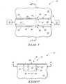
- FIG. 1is a diagrammatic, cross-sectional top view of an optical device assembly in accordance with an exemplary aspect of the present invention.
- FIG. 2is a diagrammatic, cross-sectional view along the line 2 - 2 of FIG. 1 .
- FIG. 3is a diagrammatic, cross-sectional top view of an optical device assembly in accordance with another exemplary aspect of the present invention.
- FIG. 4is a diagrammatic, cross-sectional view of a fragment of a semiconductor construction at a preliminary processing stage in accordance with an exemplary aspect of the present invention.
- FIG. 5is a view of the fragment of FIG. 4 shown at a processing stage subsequent to that of FIG. 4 .
- FIG. 6is a view of the fragment of FIG. 4 shown at a processing stage subsequent to that of FIG. 5 .
- FIG. 7is a view of the fragment of FIG. 4 shown at a processing stage subsequent to that of FIG. 6 .
- FIG. 8is a view of the fragment of FIG. 4 shown at a processing stage subsequent to that of FIG. 7 .
- FIG. 9is a top view of an exemplary construction comprising the fragment of FIG. 8 along the line 8 - 8 .
- FIG. 10is a view of the fragment of FIG. 4 shown at a processing stage subsequent to that of FIG. 8 .
- the inventionincludes optical waveguides and optical amplifiers, and methods of forming optical waveguides and optical amplifiers.
- rare earth elementscan be utilized to amplify optical signals.
- the rare earth elementscan be incorporated into optical interconnects, and in particular aspects into integrated circuit optical interconnects, to maintain signal strength of optical signals migrating along the optical interconnects.
- the rare earth elementscan be utilized to amplify optical signal strength within at least a segment of an optical interconnect.
- the rare earth elementscan be considered to be incorporated within light-conducting conduits, with the term “light-conducting conduit” being utilized to generically refer to any device having a path for light, including optical waveguides and optical amplifiers.
- a mechanism by which rare earth elements can amplify optical signals, or at least assist in maintaining optical signals,is that the elements can produce additional photons having the same phase and trajectory as photons which impact the elements.
- One aspect of the present inventionis a recognition that incorporation of rare earth elements in on-chip integrated circuit optical interconnect waveguides can be advantageous, particularly if the rare earth elements are within silicon nanocrystals.
- the rare earth elements in silicon nanocrystals dispersed in a dielectric (such as silicon dioxide)can lead to light amplification when the rare earth elements are excited by photons of appropriate energy.
- a dielectricsuch as silicon dioxide
- Suchcan, for example, produce emission at about 1540 nm wavelength at room temperature with an estimated excitation cross-section of 1 ⁇ 10 ⁇ 14 per square centimeter. This effect can be utilized to enhance the quantum efficiency by which light is transferred through a material.
- Erbium, ytterbium, neodymium and ceriumcan be particularly suitable for incorporation into dielectric waveguide materials.
- Erbium ionsfor example, have quantum levels that allow excitation at 800 nm wavelength, 980 nm wavelength, and 1480 nm wavelength.
- Rare earth elementstend to have low solubility in the commonly-utilized dielectrics of integrated circuitry (such as, for example, silicon dioxide). Such can be beneficial, as interstitial rare earth elements (such as, for example, erbium) will not substantially alter physical properties of the dielectric (for instance, refractive index and dielectric constant).
- FIGS. 1 and 2such illustrate a construction 10 comprising a light-conducting conduit 12 extending from an optical signal input 14 to an optical signal receiver 16 .
- the optical signal inputcan be anything that directs an optical signal into conduit 12
- the optical signal receiver 16can be anything into which an optical signal from conduit 12 is fed.
- the input 14can correspond to a fiber-optic cable, and appropriate lenses and/or other devices can be provided between the input and conduit 12 so that an optical signal from the fiber-optic cable is transferred to conduit 12 .
- the receiver 16can correspond to a fiber-optic cable, and appropriate lenses and/or other devices can be provided between the receiver and conduit 12 so that an optical signal from the conduit is transferred to the fiber-optic cable.
- input 14can correspond to a high-frequency processor directing an optical data signal to conduit 12
- receiver 16can correspond to a system configured to store or utilize the data contained in the optical data signal.
- the light-directing conduit 12is shown to be supported by a substrate 18 .
- a substratecan be anything suitable for supporting the light-directing conduit, and in some aspects can comprise monocrystalline silicon.
- the substratecan be referred to as a semiconductor substrate.
- semiconductor substratethe terms “semiconductive substrate” and “semiconductor substrate” are defined to mean any construction comprising semiconductive material, including, but not limited to, bulk semiconductive materials such as a semiconductive wafer (either alone or in assemblies comprising other materials thereon), and semiconductive material layers (either alone or in assemblies comprising other materials).
- substraterefers to any supporting structure, including, but not limited to, semiconductive substrates. It can be advantageous for the substrate to be a semiconductor substrate, in that such can allow semiconductor processing technologies to be utilized for fabrication of the light-directing conduit.
- the substrate 18can homogeneously be a semiconductor composition (as shown), or can comprise multiple layers of different compositions. If the substrate is homogeneously a semiconductor composition, the substrate can, for example, comprise, consist essentially of or consist of monocrystalline silicon. If the substrate comprises multiple layers, one or more of the layers can comprise, consist essentially of, or consist of monocrystalline silicon, and others of the layers may or may not comprise semiconductor materials. For instance, other layers may comprise dielectric materials, metallic materials, or electrically-conductive metal-containing compositions. In aspects in which the substrate comprises multiple layers, the conduit 12 can be formed in any suitable layer, or can extend through more than one layer.
- the light-directing conduit 12is shown to comprise an inner material 20 and a sheath 22 surrounding such inner material.
- the light-conducting conduitextends into substrate 18 .
- the sheathcomprises a first portion 24 between inner material 20 and substrate 18 , and a second portion 26 over the inner material 20 and substrate 18 .
- the first and second portions 24 and 26can comprise the same composition as one another, or can differ from one another in composition. Further, although the first and second portions 24 and 26 are shown to be homogeneous, it is be understood that at least one of the portions can comprise multiple differing compositions arranged as various segments or layers within such portion.
- the inner material 20can be considered to be the optical waveguide of the light-conducting conduit 12 . Light migrates through the inner material.
- the particular wavelengths of light which migrate through the inner materialcan be determined by the composition of the inner material, as will be recognized by persons of ordinary skill in the art.
- One aspect of the present inventionis a recognition that inclusion of one or more rare earth elements (in other words, one or more of the elements selected from the group consisting of cerium, praseodymium, neodymium, promethium, samarium, europium, gadolinium, terbium, dysprosium, holmium, erbium, thulium, ytterbium and lutetium) within the inner material can enhance stability of an optical signal migrating through the inner material.
- rare earth elementsin other words, one or more of the elements selected from the group consisting of cerium, praseodymium, neodymium, promethium, samarium, europium, gadolinium, terbium, dysprosium, holmium, erbium, thulium, ytterbium and lutetium
- the inner materialcan comprise a matrix having one or more rare earth elements dispersed therein, with a total concentration of the one or more rare earth elements within at least a portion of the matrix being at least about 1 ⁇ 10 16 atoms/cm 3 .
- the matrixcan comprise any suitable composition or combination of compositions, and in some aspects will comprise one or more of silicon dioxide, silicon-oxide-containing glass (for instance, borophosphosilicate glass (BPSG), phosphosilicate glass (PSG) and fluorosilicate glass (FSG)), silicon nitride, indium tin oxide and zinc tin oxide.
- silicon-oxide-containing glassescan be considered to be doped silicon dioxide, and in some aspects can be considered to consist of silicon dioxide and one or more of phosphorus, fluorine and boron.
- the rare earth elementscan be provided to any suitable concentration within the inner material matrix to assist in maintaining stability of an optical signal migrating through the inner material matrix (or, if desired, to amplify an optical signal migrating through the inner material matrix).
- the rare earth elementswill typically be provided to a concentration less than or equal to the solid solubility limit of the rare earth elements within the inner material matrix, which will typically mean that a total concentration of the rare earth elements will be less than or equal to about 1 ⁇ 10 18 atoms/cm 3 .
- a total concentration of the rare earth elements within the inner material matrixwill be from about 1 ⁇ 10 16 atoms/cm 3 to about 1 ⁇ 10 18 atoms/cm 3 .
- a particular rare earth elementwill be the only rare earth element provided within the inner material matrix, or at least will be the only rare earth element present within limits of fabrication techniques. If a particular rare earth element is the only rare earth element present within limits of fabrication techniques, such rare earth element can be considered to be substantially solely the only rare earth element present within the inner material. In some aspects, it can be advantageous for the inner material matrix to substantially solely comprise erbium or cerium.
- the earth elementscan be provided within silicon nanocrystals present within the inner material matrix.
- erbiumcan be present in the inner material matrix within erbium-rich (or erbium-doped) silicon nanocrystals.
- Sheath 22is configured to substantially keep light migrating along a path defined by the inner material 20 .
- the sheathwill typically comprise one or more compositions having a refractive index different from the refractive index of the inner material 20 adjacent such compositions. The difference between the refractive index of the sheath and that of the inner material adjacent the sheath can help retain light along a path defined by the inner material, as will be recognized by persons of ordinary skill in the art.
- composition, or compositions, of sheath 22can be anything suitable for helping to retain light along a path defined by inner material 20 .
- inner material 20comprises silicon dioxide
- the portion of sheath 22 adjacent the silicon oxidecan comprise silicon nitride and/or metallic materials and/or metal-containing compositions.
- sheath 22comprises segments of non-metallic material 34 , and segments of metallic material 32 .
- the metallic material 32can be any suitable composition or combination of compositions, and in particular aspects can comprise one or more of aluminum, tungsten, copper, and metallic silicides (for example, titanium silicide and tungsten silicide).
- the waveguide 20can be considered to have a longitudinal dimension extending along a longitudinal axis 21 ( FIG. 1 ), and to have lateral dimensions (for instance, the lateral dimensions 23 and 25 of FIGS. 1 and 2 ) which are orthogonal to the longitudinal dimension.
- sheath 22extends entirely around the lateral dimensions of waveguide 20 , and accordingly entirely surrounds such lateral dimensions.
- the inner material 20will have a region (or segment) doped with a sufficient concentration of one or more rare earth elements to amplify an optical signal (which will typically be a total concentration of at least about 1 ⁇ 10 16 atoms/cm 3 of the rare earth elements), and will have another region (or segment) which is not doped to any significant amount with rare earth elements (or in other words, which has a total concentration of rare earth elements of less than 1 ⁇ 10 15 atoms/cm 3 ).
- an optical signalwhich will typically be a total concentration of at least about 1 ⁇ 10 16 atoms/cm 3 of the rare earth elements
- another region (or segment)which is not doped to any significant amount with rare earth elements (or in other words, which has a total concentration of rare earth elements of less than 1 ⁇ 10 15 atoms/cm 3 ).
- FIG. 3Such aspect of the invention is illustrated in FIG. 3 .
- similar numberingwill be used as is utilized above in describing FIGS. 1 and 2 , where appropriate.
- FIG. 3shows a construction 40 comprising a light-conducting conduit 42 supported by a substrate 18 .
- the substrate 18can be identical to that described previously with reference to FIGS. 1 and 2 .
- the optical signal input 14 and optical signal receiver 16 discussed aboveare shown proximate light-conducting conduit 42 .
- An optical signal provided from input 14passes through conduit 42 to the receiver 16 , and accordingly a path of light through the conduit can be considered to proceed downstream from input 14 to receiver 16 .
- the light-conducting conduit 42comprises two adjacent segments 44 and 46 of a waveguide, with the segment 44 being upstream of the segment 46 relative to the flow of light through the conduit to the receiver 16 .
- the upstream segment 44can be doped with a sufficient concentration of one or more rare earth elements to amplify an optical signal (which typically will be a total concentration of at least about 1 ⁇ 10 16 atoms/cm 3 of the rare earth elements; and can be a total concentration of the rare earth elements of from about 1 ⁇ 10 16 atoms/cm 3 to about 1 ⁇ 10 18 atoms/cm 3 ), while the downstream segment 46 is not doped to any significant amount with rare earth elements (which typically will be a total concentration of rare earth elements of less than 1 ⁇ 10 15 atoms/cm 3 ).
- the construction 40can be considered to comprise an optical signal propagation assembly.
- the upstream segment 44 of such assemblycan be considered an optical signal amplifier which receives an optical signal from input 14 and utilizes the rare earth elements therein to amplify the signal prior to passing the signal through the remaining segment 46 of the conduit to the receiver 16 .
- the segments 44 and 46 of the waveguidecan comprise compositions similar to those discussed above regarding waveguide 20 , and specifically can comprise dielectric matrix material having one or more rare earth elements dispersed therein.
- at least some of such earth elementscan be provided in rare-earth-element-rich silicon nanocrystals. Any suitable rare earth elements or combinations of rare earth elements can be utilized.
- one or more of erbium, cerium, neodymium and ytterbiumwill be utilized.
- the dielectric matrix material of segment 44will differ from that of segment 46 .
- the segment 44will comprise one or both of indium tin oxide and zinc tin oxide, and the segment 46 will not comprise indium tin oxide or zinc tin oxide.
- the dielectric matrix material of segment 46can, for example, comprise one or more of silicon dioxide, doped silicon dioxide, and silicon nitride.
- a sheath 48is shown along lateral edges of segments 44 and 46 .
- the exemplary sheath 48has metallic regions 32 and non-metallic regions 34 .
- Such exemplary sheathis shown to indicate that the sheath utilized in the construction of FIG. 3 can, like the sheath utilized in the construction of FIGS. 1 and 2 , comprise non-metallic segments, metallic segments, or combinations of non-metallic segment and metallic segments.
- the metallic material of sheath 48is shown adjacent the segment 44 enriched in rare earth elements, it is to be understood that portions of the sheath adjacent the segment 46 can also be metallic.
- the sheath 48 of FIG. 3can entirely laterally surround the waveguide containing segments 44 and 46 analogously to the way that the sheath 22 entirely laterally surrounds the waveguide 20 of FIGS. 1 and 2 .
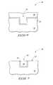
- FIGS. 4-10An exemplary method for forming an exemplary optical signal conduit of the present invention is described with reference to FIGS. 4-10 .
- similar numberingwill be used as is utilized above in describing FIGS. 1-3 , where appropriate.
- a construction 40is shown to comprise a substrate 18 .
- Such substratecan be a semiconductor substrate, and in some aspects can comprise, consist essentially of, or consist of bulk monocrystalline silicon.
- a trench 50is etched into substrate 18 . Although only one trench is shown, it is to be understood that multiple trenches could be simultaneously formed within the substrate.
- Trench 50can be formed with any suitable processing, including, for example, provision of a photolithographically patterned mask (not shown) defining the location of the trench; an etch into the substrate to form the trench in the location defined by the mask; and subsequent removal of the mask to leave the structure shown in FIG. 5 .
- trench 50is lined with a barrier material 54 , and the lined trench is then filled with waveguide material 56 .
- all of the trenchescan be lined with material 54 and filled with material 56 , or alternatively fewer than all of the trenches can be lined with material 54 and/or filled with material 56 .
- Barrier material 54is a barrier relative to light traveling down a waveguide comprising material 56 . The barrier may absolutely impede light from escaping for the waveguide, but more typically only partially impedes light from escaping from the waveguide.
- Barrier material 54ultimately forms the sheath discussed above, and accordingly can comprise the same compositions as described previously for the sheathing materials of FIGS. 1-3 .
- the barrier materialcan, for example, comprise silicon nitride or other non-metallic materials and/or can comprise various metallic materials.
- Waveguide material 56ultimately forms a light-conducting conduit analogous to the light-conducting conduits discussed above, and accordingly can comprise the same compositions as described previously for the light-conducting conduits of FIGS. 1-3 .
- the waveguide materialcan, for example, comprise, consist essentially of, or consist of one or more of silicon dioxide, doped silicon dioxide, silicon nitride, indium tin oxide, and zinc tin oxide.
- materials 54 and 56are subjected to planarization (such as, for example, chemical-mechanical polishing) to form a planarized upper surface 57 extending across substrate 18 and materials 54 and 56 .
- planarizationcan, in some aspects, remove some of substrate 18 so that the planarized surface 57 is elevationally below an initial uppermost surface of substrate 18 , and in other aspects can substantially stop upon reaching an uppermost surface of substrate 18 .
- waveguide material 56( FIG. 7 ) is exposed to one or more rare earth elements to convert the material to rare-earth-element-doped material 60 .
- the doping with rare earth elementsis shown occurring after the planarization of FIG. 7 , it is to be understood that the invention also includes aspects (not shown) in which such doping occurs before the planarization.
- any suitable methodcan be utilized for incorporating desired rare earth elements into the waveguide material.
- dopantcan be implanted into the material.
- chlorides of one or more rare earth elementsare implanted into the material utilizing an implantation energy of from about 100 KeV to about 300 KeV, and an implant dose of from about 1 ⁇ 10 13 atoms/cm 2 to about 1 ⁇ 10 15 atoms/cm 2 .
- Such implantationcan achieve the desired dose of rare earth element within the waveguide material of from about 1 ⁇ 10 16 atoms/cm 3 to about 1 ⁇ 10 18 atoms/cm 3 .
- the implantationcan be followed with an anneal at, for example, a temperature of from about 500° C. to about 700° C.
- the implanted rare earth elementcan be erbium, and the chloride can therefore be erbium chloride. If the implanted rare earth element is entirely erbium, the dopant within the waveguide material can be solely erbium; and if the implanted rare earth element is at least nearly entirely erbium, the dopant within the waveguide material can be at least substantially solely erbium.
- the waveguide materialcan be doped by exposing the waveguide material to an acidic solution having rare-earth-element-containing material dissolved therein.
- acidic solutioncan, for example, correspond to a solution formed of a 1:1 volume dilution of 36% (by weight) HCl in water, having one or more of erbium oxide (Er 2 O 3 ), cerium oxide (CeO 2 ), or various organic/rare earth element compounds dissolved therein.
- the dopingcan be followed with the above-described anneal to diffuse the rare earth elements within the waveguide material.
- some aspects of the inventioncomprise incorporation of the rare earth elements within silicon nanocrystals of the waveguide material. Such incorporation can occur during the anneal if the waveguide material comprises some silicon. Accordingly, some aspects of the invention will comprise incorporation of some silicon with the dielectric material utilized as waveguide material.
- the waveguide materialcan primarily comprise one or more of silicon dioxide, doped silicon dioxide, silicon nitride, indium tin oxide, and zinc tin oxide; and can further comprise sufficient silicon so that silicon nanocrystals are dispersed within the waveguide material in sufficient quantity to incorporate most or all of the rare earth element that is ultimately provided within the waveguide material.
- the doping described with reference to FIG. 8can dope an entirety of the waveguide material, or only a portion of the waveguide material. For instance, some of the waveguide material can be protected with a mask during the doping so that the protected portion is not doped while another portion is doped.
- FIG. 9shows atop view of an exemplary construction at the processing stage of FIG. 8 in which one portion of the waveguide material is doped to form the doped material 60 , and another portion (or segment) of the waveguide material is not doped (and accordingly remains as the material 56 discussed above with reference to FIGS. 6 and 7 ).
- FIG. 9comprises an optical signal propagation assembly analogous to the assembly discussed above with reference to FIG. 3 .
- the segment 60 of FIG. 9can have an identical composition as discussed above for the segment 44 of FIG. 3
- the segment 56 of FIG. 9can have an identical composition as discussed above for the segment 46 of FIG. 3 .
- segment 60can correspond to one or both of rare-earth-element-doped indium tin oxide and rare-earth-element-doped zinc tin oxide
- segment 56can correspond to one or more of silicon dioxide, doped silicon dioxide and silicon nitride.
- barrier material 54is shown comprising a common composition along the segment 60 as along segment 56 , the invention includes some aspects in which the barrier material is different along the doped waveguide material than along the undoped waveguide material. For instance, it may be advantageous to utilize metallic barrier materials along the doped waveguide material comprising indium tin oxide or zinc tin oxide, and to utilize non-metallic barrier materials along the undoped waveguide material comprising silicon dioxide, doped silicon dioxide and/or silicon nitride.
- FIG. 10the cross-section of FIG. 8 is shown at a processing stage subsequent that of FIGS. 8 and 9 , and specifically is shown after a second barrier material 62 is formed across the planarized surface 57 .
- the second barrier materialcontacts the first barrier material along sidewalls of the trench 50 (such trench is described above with reference to FIG. 5 ).
- the second barrier materialcan, like the first barrier material, comprise a single composition, or can comprise segments of differing composition.
- the second barrier materialcan, in some aspects, be compositionally the same as the first barrier material where the second barrier material contacts the first barrier material.
Landscapes
- Physics & Mathematics (AREA)
- General Physics & Mathematics (AREA)
- Optics & Photonics (AREA)
- Engineering & Computer Science (AREA)
- Microelectronics & Electronic Packaging (AREA)
- Lasers (AREA)
- Optical Integrated Circuits (AREA)
Abstract
Description
Claims (14)
Priority Applications (2)
| Application Number | Priority Date | Filing Date | Title |
|---|---|---|---|
| US12/849,132US8094984B2 (en) | 2006-01-17 | 2010-08-03 | Semiconductor constructions, methods of forming semiconductor constructions, light-conducting conduits, and optical signal propagation assemblies |
| US13/204,965US8630522B2 (en) | 2006-01-17 | 2011-08-08 | Constructions and light-conducting conduits |
Applications Claiming Priority (3)
| Application Number | Priority Date | Filing Date | Title |
|---|---|---|---|
| US11/332,991US7280729B2 (en) | 2006-01-17 | 2006-01-17 | Semiconductor constructions and light-directing conduits |
| US11/846,404US7776749B2 (en) | 2006-01-17 | 2007-08-28 | Methods of forming semiconductor constructions |
| US12/849,132US8094984B2 (en) | 2006-01-17 | 2010-08-03 | Semiconductor constructions, methods of forming semiconductor constructions, light-conducting conduits, and optical signal propagation assemblies |
Related Parent Applications (1)
| Application Number | Title | Priority Date | Filing Date |
|---|---|---|---|
| US11/846,404DivisionUS7776749B2 (en) | 2006-01-17 | 2007-08-28 | Methods of forming semiconductor constructions |
Related Child Applications (1)
| Application Number | Title | Priority Date | Filing Date |
|---|---|---|---|
| US13/204,965ContinuationUS8630522B2 (en) | 2006-01-17 | 2011-08-08 | Constructions and light-conducting conduits |
Publications (2)
| Publication Number | Publication Date |
|---|---|
| US20100296158A1 US20100296158A1 (en) | 2010-11-25 |
| US8094984B2true US8094984B2 (en) | 2012-01-10 |
Family
ID=38263254
Family Applications (4)
| Application Number | Title | Priority Date | Filing Date |
|---|---|---|---|
| US11/332,991Active2026-04-29US7280729B2 (en) | 2006-01-17 | 2006-01-17 | Semiconductor constructions and light-directing conduits |
| US11/846,404Active2027-05-10US7776749B2 (en) | 2006-01-17 | 2007-08-28 | Methods of forming semiconductor constructions |
| US12/849,132ActiveUS8094984B2 (en) | 2006-01-17 | 2010-08-03 | Semiconductor constructions, methods of forming semiconductor constructions, light-conducting conduits, and optical signal propagation assemblies |
| US13/204,965Active2026-07-07US8630522B2 (en) | 2006-01-17 | 2011-08-08 | Constructions and light-conducting conduits |
Family Applications Before (2)
| Application Number | Title | Priority Date | Filing Date |
|---|---|---|---|
| US11/332,991Active2026-04-29US7280729B2 (en) | 2006-01-17 | 2006-01-17 | Semiconductor constructions and light-directing conduits |
| US11/846,404Active2027-05-10US7776749B2 (en) | 2006-01-17 | 2007-08-28 | Methods of forming semiconductor constructions |
Family Applications After (1)
| Application Number | Title | Priority Date | Filing Date |
|---|---|---|---|
| US13/204,965Active2026-07-07US8630522B2 (en) | 2006-01-17 | 2011-08-08 | Constructions and light-conducting conduits |
Country Status (7)
| Country | Link |
|---|---|
| US (4) | US7280729B2 (en) |
| EP (1) | EP1974233B1 (en) |
| JP (1) | JP5126611B2 (en) |
| KR (1) | KR100983394B1 (en) |
| CN (1) | CN101365971B (en) |
| SG (1) | SG154428A1 (en) |
| WO (1) | WO2007087046A2 (en) |
Families Citing this family (8)
| Publication number | Priority date | Publication date | Assignee | Title |
|---|---|---|---|---|
| US7280729B2 (en) | 2006-01-17 | 2007-10-09 | Micron Technology, Inc. | Semiconductor constructions and light-directing conduits |
| JP2009272614A (en)* | 2008-04-30 | 2009-11-19 | Sharp Corp | Erbium-doped silicon nanocrystalline-embedded silicon oxide waveguide and method of manufacturing the same, and integrated circuit including the same |
| WO2015108589A2 (en) | 2013-10-22 | 2015-07-23 | Massachusetts Institute Of Technology | Waveguide formation using cmos fabrication techniques |
| US10371129B2 (en)* | 2016-02-26 | 2019-08-06 | Semiconductor Energy Laboratory Co., Ltd. | Semiconductor device and sensor system |
| GB2552636B (en)* | 2017-11-22 | 2019-01-09 | Rofin Sinar Uk Ltd | Polarisation and mode selection technique for a laser |
| EP3639730A1 (en)* | 2018-10-16 | 2020-04-22 | Koninklijke Philips N.V. | Supply of a sensor of an interventional device |
| WO2023180788A1 (en)* | 2022-03-23 | 2023-09-28 | Ecole Polytechnique Federale De Lausanne (Epfl) | Waveguide amplifier and waveguide amplifier fabrication method |
| US12276831B2 (en)* | 2022-11-28 | 2025-04-15 | Globalfoundries U.S. Inc. | Enlarged multilayer nitride waveguide for photonic integrated circuit |
Citations (18)
| Publication number | Priority date | Publication date | Assignee | Title |
|---|---|---|---|---|
| US5039199A (en) | 1989-12-29 | 1991-08-13 | At&T Bell Laboratories | Lightwave transmission system having remotely pumped quasi-distributed amplifying fibers |
| JPH06216441A (en) | 1993-01-20 | 1994-08-05 | Hitachi Cable Ltd | Fiber for optical amplifier and amplifier |
| JPH0736066A (en) | 1993-07-26 | 1995-02-07 | Hitachi Cable Ltd | Method of manufacturing waveguide type optical amplifier |
| US5397920A (en) | 1994-03-24 | 1995-03-14 | Minnesota Mining And Manufacturing Company | Light transmissive, electrically-conductive, oxide film and methods of production |
| US5463649A (en) | 1993-08-06 | 1995-10-31 | Sandia Corporation | Monolithically integrated solid state laser and waveguide using spin-on glass |
| US5563979A (en) | 1995-08-31 | 1996-10-08 | Lucent Technologies Inc. | Erbium-doped planar optical device |
| US5562838A (en) | 1993-03-29 | 1996-10-08 | Martin Marietta Corporation | Optical light pipe and microwave waveguide interconnects in multichip modules formed using adaptive lithography |
| JPH1078523A (en) | 1996-09-04 | 1998-03-24 | Nippon Telegr & Teleph Corp <Ntt> | Manufacturing method of optical waveguide |
| WO1998030507A1 (en) | 1997-01-14 | 1998-07-16 | Corning Incorporated | Glass composition and optical device made therefrom |
| US6430349B1 (en) | 1999-01-27 | 2002-08-06 | The United States Of America As Represented By The Secretary Of Commerce | High-power waveguide lasers |
| US6512879B1 (en) | 1997-01-14 | 2003-01-28 | Corning Incorporated | Glass composition and optical device made therefrom |
| US20030052082A1 (en) | 2001-09-19 | 2003-03-20 | Anisul Khan | Method of forming optical waveguides in a semiconductor substrate |
| US20030112495A1 (en) | 2001-12-13 | 2003-06-19 | Alduino Andrew C. | Optical amplifier with transverse pump |
| WO2003065093A1 (en) | 2002-01-29 | 2003-08-07 | Luxpert Technologies Co., Ltd. | Top-pumped waveguide amplifier |
| US20030174391A1 (en) | 2002-03-16 | 2003-09-18 | Tao Pan | Gain flattened optical amplifier |
| US20040136681A1 (en) | 2003-01-10 | 2004-07-15 | Novellus Systems, Inc. | Erbium-doped oxide glass |
| WO2005079395A2 (en) | 2004-02-13 | 2005-09-01 | Yin Tang | Integration of rare-earth doped amplifiers into semiconductor structures |
| US20100135627A1 (en)* | 2008-12-02 | 2010-06-03 | Draka Comteq, B.V. | Amplifying Optical Fiber and Production Method |
Family Cites Families (6)
| Publication number | Priority date | Publication date | Assignee | Title |
|---|---|---|---|---|
| FR2683948B1 (en) | 1991-11-20 | 1994-03-04 | France Telecom | INTEGRATED OPTICAL COMPONENT STRUCTURE CONTAINING RARE EARTH, PRODUCTION METHOD AND APPLICATIONS. |
| US6567209B2 (en)* | 2000-05-22 | 2003-05-20 | Massachusetts Institute Of Technology | Microcavity amplifiers |
| US20020181914A1 (en)* | 2001-04-27 | 2002-12-05 | Jansen David B. | Method and apparatus for decreasing signal propagation delay in a waveguide |
| WO2004066346A2 (en)* | 2003-01-22 | 2004-08-05 | Group Iv Semiconductor Inc. | Rare earth doped group iv nanocrystal layers |
| KR100594036B1 (en)* | 2003-12-30 | 2006-06-30 | 삼성전자주식회사 | Optical signal amplification apparatus, optical communication module having same and manufacturing method thereof |
| US7280729B2 (en) | 2006-01-17 | 2007-10-09 | Micron Technology, Inc. | Semiconductor constructions and light-directing conduits |
- 2006
- 2006-01-17USUS11/332,991patent/US7280729B2/enactiveActive
- 2006-12-15EPEP06845726.6Apatent/EP1974233B1/enactiveActive
- 2006-12-15KRKR1020087016962Apatent/KR100983394B1/enactiveActive
- 2006-12-15WOPCT/US2006/048261patent/WO2007087046A2/enactiveApplication Filing
- 2006-12-15JPJP2008550317Apatent/JP5126611B2/enactiveActive
- 2006-12-15CNCN2006800511903Apatent/CN101365971B/enactiveActive
- 2006-12-15SGSG200904435-5Apatent/SG154428A1/enunknown
- 2007
- 2007-08-28USUS11/846,404patent/US7776749B2/enactiveActive
- 2010
- 2010-08-03USUS12/849,132patent/US8094984B2/enactiveActive
- 2011
- 2011-08-08USUS13/204,965patent/US8630522B2/enactiveActive
Patent Citations (22)
| Publication number | Priority date | Publication date | Assignee | Title |
|---|---|---|---|---|
| US5039199A (en) | 1989-12-29 | 1991-08-13 | At&T Bell Laboratories | Lightwave transmission system having remotely pumped quasi-distributed amplifying fibers |
| JPH04120524A (en) | 1989-12-29 | 1992-04-21 | American Teleph & Telegr Co <Att> | Optical transmission system |
| JPH06216441A (en) | 1993-01-20 | 1994-08-05 | Hitachi Cable Ltd | Fiber for optical amplifier and amplifier |
| US5562838A (en) | 1993-03-29 | 1996-10-08 | Martin Marietta Corporation | Optical light pipe and microwave waveguide interconnects in multichip modules formed using adaptive lithography |
| JPH0736066A (en) | 1993-07-26 | 1995-02-07 | Hitachi Cable Ltd | Method of manufacturing waveguide type optical amplifier |
| US5463649A (en) | 1993-08-06 | 1995-10-31 | Sandia Corporation | Monolithically integrated solid state laser and waveguide using spin-on glass |
| US5397920A (en) | 1994-03-24 | 1995-03-14 | Minnesota Mining And Manufacturing Company | Light transmissive, electrically-conductive, oxide film and methods of production |
| US5563979A (en) | 1995-08-31 | 1996-10-08 | Lucent Technologies Inc. | Erbium-doped planar optical device |
| JPH09105965A (en) | 1995-08-31 | 1997-04-22 | At & T Corp | Optical device |
| JPH1078523A (en) | 1996-09-04 | 1998-03-24 | Nippon Telegr & Teleph Corp <Ntt> | Manufacturing method of optical waveguide |
| WO1998030507A1 (en) | 1997-01-14 | 1998-07-16 | Corning Incorporated | Glass composition and optical device made therefrom |
| JP2001508392A (en) | 1997-01-14 | 2001-06-26 | コーニング インコーポレイテッド | Glass composition and optical element produced therefrom |
| US6512879B1 (en) | 1997-01-14 | 2003-01-28 | Corning Incorporated | Glass composition and optical device made therefrom |
| US6430349B1 (en) | 1999-01-27 | 2002-08-06 | The United States Of America As Represented By The Secretary Of Commerce | High-power waveguide lasers |
| US20030052082A1 (en) | 2001-09-19 | 2003-03-20 | Anisul Khan | Method of forming optical waveguides in a semiconductor substrate |
| US20030112495A1 (en) | 2001-12-13 | 2003-06-19 | Alduino Andrew C. | Optical amplifier with transverse pump |
| WO2003065093A1 (en) | 2002-01-29 | 2003-08-07 | Luxpert Technologies Co., Ltd. | Top-pumped waveguide amplifier |
| US20030174391A1 (en) | 2002-03-16 | 2003-09-18 | Tao Pan | Gain flattened optical amplifier |
| US20040136681A1 (en) | 2003-01-10 | 2004-07-15 | Novellus Systems, Inc. | Erbium-doped oxide glass |
| WO2005079395A2 (en) | 2004-02-13 | 2005-09-01 | Yin Tang | Integration of rare-earth doped amplifiers into semiconductor structures |
| US20050195472A1 (en) | 2004-02-13 | 2005-09-08 | Tang Yin S. | Integration of rare-earth doped amplifiers into semiconductor structures and uses of same |
| US20100135627A1 (en)* | 2008-12-02 | 2010-06-03 | Draka Comteq, B.V. | Amplifying Optical Fiber and Production Method |
Non-Patent Citations (10)
| Title |
|---|
| Characteristics of rare-earth element erbium implanted in silicon; Tang et al; 1989 American Institute of Physics; Appl. Phys. Lett. 55 (5), Jul. 31, 1989 pp. 432-433. |
| Chelnokove et al., Deep High Dose Erbium Implantation of Low Loss Silicon Oxynitride Waveguides, 1994, Electronics Letters, vol. 30 No. 22 pp. 1850-1852. |
| Chen et al., Indium Tin Oxide Single Mode Waveguide Modulator, 1991, Intergrated Optical Circuits, vol. 1583, pp. 362-374. |
| Chen et al., Optoelectronic Property of PN Junction on Erbium Doped Silicon Using Thermal Diffusion Method, 2003, Solid State Electronics, No. 47, pp. 2127-2130. |
| Electroluminescence at 1.54 .mu.m in Er-doped Si nanocluster-based devices; F. Iacona et al.; Applied Physics Letters, vol. 8, No. 17; Oct. 21, 2002; pp. 3242-3244. |
| Ibanga et al., Zinc Oxide Waveguide Produced by Thermal Oxidation of Chemical Bath Deposited Zinc Sulphide Thin Films, No. 80, pp. 490-495. |
| PCT/US2006/048261, Aug. 7, 2008, Search Report. |
| PCT/US2006/048261, Aug. 7, 2008, Written Opinion. |
| Stutius et al., Silicon Nitride Films on Silicon for Optical Waveguides, 1977, Applied Optics, vol. 16 No. 12, pp. 3218-3222. |
| Wu et al., Ion Beam Synthesis of Heteroepitaxial Erbium Silicide Layers, 1996, Applied Surface Science, No. 102, pp. 184-188. |
Also Published As
| Publication number | Publication date |
|---|---|
| JP2009524214A (en) | 2009-06-25 |
| US20070165992A1 (en) | 2007-07-19 |
| EP1974233A2 (en) | 2008-10-01 |
| JP5126611B2 (en) | 2013-01-23 |
| US8630522B2 (en) | 2014-01-14 |
| SG154428A1 (en) | 2009-08-28 |
| US20070295686A1 (en) | 2007-12-27 |
| US20110293233A1 (en) | 2011-12-01 |
| US7776749B2 (en) | 2010-08-17 |
| KR100983394B1 (en) | 2010-09-20 |
| US20100296158A1 (en) | 2010-11-25 |
| US7280729B2 (en) | 2007-10-09 |
| CN101365971B (en) | 2012-05-30 |
| KR20080078712A (en) | 2008-08-27 |
| WO2007087046A3 (en) | 2008-10-02 |
| CN101365971A (en) | 2009-02-11 |
| WO2007087046A2 (en) | 2007-08-02 |
| EP1974233B1 (en) | 2013-05-08 |
Similar Documents
| Publication | Publication Date | Title |
|---|---|---|
| US8630522B2 (en) | Constructions and light-conducting conduits | |
| EP2988338B1 (en) | Semiconductor light-receiving element and method for manufacturing same | |
| US8242432B2 (en) | System having light sensor with enhanced sensitivity including a multiplication layer for generating additional electrons | |
| KR0183886B1 (en) | Trench device isolation method of semiconductor device | |
| US8923665B2 (en) | Material structures for front-end of the line integration of optical polarization splitters and rotators | |
| JPH09105965A (en) | Optical device | |
| US6140244A (en) | Method for forming a spacer | |
| US20090101626A1 (en) | Selective etching bath methods | |
| US6911394B2 (en) | Semiconductor devices and methods of manufacturing such semiconductor devices | |
| US6399478B2 (en) | Method of making a dual damascene structure with modified insulation | |
| EP0817248A2 (en) | Method of manufacturing SOI substrate | |
| CN102347229A (en) | Semiconductor devices and method of forming the same | |
| US20080017928A1 (en) | Semiconductor Device and Method for Manufacturing the Same | |
| US7205624B2 (en) | Self-aligned implanted waveguide detector | |
| US20050214964A1 (en) | Sige super lattice optical detectors | |
| JPH07297276A (en) | Formation of semiconductor integrated circuit | |
| JP2004037990A (en) | Optical waveguide and its manufacturing method | |
| KR100610436B1 (en) | Method for suppressing deterioration of gate oxide film | |
| JP2004095839A (en) | Waveguide optical amplifier and its manufacturing method | |
| KR100587674B1 (en) | Transistor Structure in Semiconductor Device and Formation Method | |
| CN117766606A (en) | Photoelectric detector, preparation method thereof and photoelectric communication device | |
| KR20210104876A (en) | Process for manufacturing the substrate for the front image sensor | |
| KR20060120962A (en) | Bit line contact formation method of semiconductor device |
Legal Events
| Date | Code | Title | Description |
|---|---|---|---|
| FEPP | Fee payment procedure | Free format text:PAYOR NUMBER ASSIGNED (ORIGINAL EVENT CODE: ASPN); ENTITY STATUS OF PATENT OWNER: LARGE ENTITY | |
| STCF | Information on status: patent grant | Free format text:PATENTED CASE | |
| FPAY | Fee payment | Year of fee payment:4 | |
| AS | Assignment | Owner name:U.S. BANK NATIONAL ASSOCIATION, AS COLLATERAL AGENT, CALIFORNIA Free format text:SECURITY INTEREST;ASSIGNOR:MICRON TECHNOLOGY, INC.;REEL/FRAME:038669/0001 Effective date:20160426 Owner name:U.S. BANK NATIONAL ASSOCIATION, AS COLLATERAL AGEN Free format text:SECURITY INTEREST;ASSIGNOR:MICRON TECHNOLOGY, INC.;REEL/FRAME:038669/0001 Effective date:20160426 | |
| AS | Assignment | Owner name:MORGAN STANLEY SENIOR FUNDING, INC., AS COLLATERAL AGENT, MARYLAND Free format text:PATENT SECURITY AGREEMENT;ASSIGNOR:MICRON TECHNOLOGY, INC.;REEL/FRAME:038954/0001 Effective date:20160426 Owner name:MORGAN STANLEY SENIOR FUNDING, INC., AS COLLATERAL Free format text:PATENT SECURITY AGREEMENT;ASSIGNOR:MICRON TECHNOLOGY, INC.;REEL/FRAME:038954/0001 Effective date:20160426 | |
| AS | Assignment | Owner name:U.S. BANK NATIONAL ASSOCIATION, AS COLLATERAL AGENT, CALIFORNIA Free format text:CORRECTIVE ASSIGNMENT TO CORRECT THE REPLACE ERRONEOUSLY FILED PATENT #7358718 WITH THE CORRECT PATENT #7358178 PREVIOUSLY RECORDED ON REEL 038669 FRAME 0001. ASSIGNOR(S) HEREBY CONFIRMS THE SECURITY INTEREST;ASSIGNOR:MICRON TECHNOLOGY, INC.;REEL/FRAME:043079/0001 Effective date:20160426 Owner name:U.S. BANK NATIONAL ASSOCIATION, AS COLLATERAL AGEN Free format text:CORRECTIVE ASSIGNMENT TO CORRECT THE REPLACE ERRONEOUSLY FILED PATENT #7358718 WITH THE CORRECT PATENT #7358178 PREVIOUSLY RECORDED ON REEL 038669 FRAME 0001. ASSIGNOR(S) HEREBY CONFIRMS THE SECURITY INTEREST;ASSIGNOR:MICRON TECHNOLOGY, INC.;REEL/FRAME:043079/0001 Effective date:20160426 | |
| AS | Assignment | Owner name:JPMORGAN CHASE BANK, N.A., AS COLLATERAL AGENT, ILLINOIS Free format text:SECURITY INTEREST;ASSIGNORS:MICRON TECHNOLOGY, INC.;MICRON SEMICONDUCTOR PRODUCTS, INC.;REEL/FRAME:047540/0001 Effective date:20180703 Owner name:JPMORGAN CHASE BANK, N.A., AS COLLATERAL AGENT, IL Free format text:SECURITY INTEREST;ASSIGNORS:MICRON TECHNOLOGY, INC.;MICRON SEMICONDUCTOR PRODUCTS, INC.;REEL/FRAME:047540/0001 Effective date:20180703 | |
| AS | Assignment | Owner name:MICRON TECHNOLOGY, INC., IDAHO Free format text:RELEASE BY SECURED PARTY;ASSIGNOR:U.S. BANK NATIONAL ASSOCIATION, AS COLLATERAL AGENT;REEL/FRAME:047243/0001 Effective date:20180629 | |
| MAFP | Maintenance fee payment | Free format text:PAYMENT OF MAINTENANCE FEE, 8TH YEAR, LARGE ENTITY (ORIGINAL EVENT CODE: M1552); ENTITY STATUS OF PATENT OWNER: LARGE ENTITY Year of fee payment:8 | |
| AS | Assignment | Owner name:MICRON TECHNOLOGY, INC., IDAHO Free format text:RELEASE BY SECURED PARTY;ASSIGNOR:MORGAN STANLEY SENIOR FUNDING, INC., AS COLLATERAL AGENT;REEL/FRAME:050937/0001 Effective date:20190731 | |
| AS | Assignment | Owner name:MICRON TECHNOLOGY, INC., IDAHO Free format text:RELEASE BY SECURED PARTY;ASSIGNOR:JPMORGAN CHASE BANK, N.A., AS COLLATERAL AGENT;REEL/FRAME:051028/0001 Effective date:20190731 Owner name:MICRON SEMICONDUCTOR PRODUCTS, INC., IDAHO Free format text:RELEASE BY SECURED PARTY;ASSIGNOR:JPMORGAN CHASE BANK, N.A., AS COLLATERAL AGENT;REEL/FRAME:051028/0001 Effective date:20190731 | |
| MAFP | Maintenance fee payment | Free format text:PAYMENT OF MAINTENANCE FEE, 12TH YEAR, LARGE ENTITY (ORIGINAL EVENT CODE: M1553); ENTITY STATUS OF PATENT OWNER: LARGE ENTITY Year of fee payment:12 |