US8093597B2 - In situ dopant implantation and growth of a III-nitride semiconductor body - Google Patents
In situ dopant implantation and growth of a III-nitride semiconductor bodyDownload PDFInfo
- Publication number
- US8093597B2 US8093597B2US12/661,342US66134210AUS8093597B2US 8093597 B2US8093597 B2US 8093597B2US 66134210 AUS66134210 AUS 66134210AUS 8093597 B2US8093597 B2US 8093597B2
- Authority
- US
- United States
- Prior art keywords
- iii
- nitride semiconductor
- semiconductor body
- nitride
- growth
- Prior art date
- Legal status (The legal status is an assumption and is not a legal conclusion. Google has not performed a legal analysis and makes no representation as to the accuracy of the status listed.)
- Expired - Fee Related
Links
- 239000004065semiconductorSubstances0.000titleclaimsabstractdescription97
- 239000002019doping agentSubstances0.000titleclaimsabstractdescription61
- 238000002513implantationMethods0.000titleclaimsabstractdescription43
- 238000011065in-situ storageMethods0.000titleclaimsabstractdescription23
- 238000000034methodMethods0.000claimsabstractdescription28
- 239000002131composite materialSubstances0.000claimsabstractdescription21
- 239000000758substrateSubstances0.000claimsabstractdescription10
- 230000007704transitionEffects0.000claimsdescription18
- 230000008569processEffects0.000claimsdescription9
- 238000001451molecular beam epitaxyMethods0.000claimsdescription5
- 238000005229chemical vapour depositionMethods0.000claimsdescription3
- 230000005669field effectEffects0.000claimsdescription3
- 230000015572biosynthetic processEffects0.000claimsdescription2
- JMASRVWKEDWRBT-UHFFFAOYSA-NGallium nitrideChemical compound[Ga]#NJMASRVWKEDWRBT-UHFFFAOYSA-N0.000claims2
- 229910002601GaNInorganic materials0.000description37
- 150000002500ionsChemical class0.000description11
- 239000000463materialSubstances0.000description8
- IJGRMHOSHXDMSA-UHFFFAOYSA-NAtomic nitrogenChemical compoundN#NIJGRMHOSHXDMSA-UHFFFAOYSA-N0.000description6
- 238000013459approachMethods0.000description6
- 239000007789gasSubstances0.000description6
- 238000004519manufacturing processMethods0.000description4
- 150000004767nitridesChemical class0.000description4
- 239000000376reactantSubstances0.000description4
- XUIMIQQOPSSXEZ-UHFFFAOYSA-NSiliconChemical compound[Si]XUIMIQQOPSSXEZ-UHFFFAOYSA-N0.000description3
- 238000004891communicationMethods0.000description3
- 238000009792diffusion processMethods0.000description3
- 229910052757nitrogenInorganic materials0.000description3
- 229910052710siliconInorganic materials0.000description3
- 239000010703siliconSubstances0.000description3
- QGZKDVFQNNGYKY-UHFFFAOYSA-NAmmoniaChemical compoundNQGZKDVFQNNGYKY-UHFFFAOYSA-N0.000description2
- 229910052581Si3N4Inorganic materials0.000description2
- 238000000137annealingMethods0.000description2
- 150000001875compoundsChemical class0.000description2
- PMHQVHHXPFUNSP-UHFFFAOYSA-Mcopper(1+);methylsulfanylmethane;bromideChemical compoundBr[Cu].CSCPMHQVHHXPFUNSP-UHFFFAOYSA-M0.000description2
- 238000000354decomposition reactionMethods0.000description2
- 238000010586diagramMethods0.000description2
- 238000010884ion-beam techniqueMethods0.000description2
- 239000011777magnesiumSubstances0.000description2
- 230000006911nucleationEffects0.000description2
- 238000010899nucleationMethods0.000description2
- 238000005086pumpingMethods0.000description2
- 238000005389semiconductor device fabricationMethods0.000description2
- HQVNEWCFYHHQES-UHFFFAOYSA-Nsilicon nitrideChemical compoundN12[Si]34N5[Si]62N3[Si]51N64HQVNEWCFYHHQES-UHFFFAOYSA-N0.000description2
- JLTRXTDYQLMHGR-UHFFFAOYSA-NtrimethylaluminiumChemical compoundC[Al](C)CJLTRXTDYQLMHGR-UHFFFAOYSA-N0.000description2
- XCZXGTMEAKBVPV-UHFFFAOYSA-NtrimethylgalliumChemical compoundC[Ga](C)CXCZXGTMEAKBVPV-UHFFFAOYSA-N0.000description2
- PIGFYZPCRLYGLF-UHFFFAOYSA-NAluminum nitrideChemical compound[Al]#NPIGFYZPCRLYGLF-UHFFFAOYSA-N0.000description1
- GYHNNYVSQQEPJS-UHFFFAOYSA-NGalliumChemical compound[Ga]GYHNNYVSQQEPJS-UHFFFAOYSA-N0.000description1
- FYYHWMGAXLPEAU-UHFFFAOYSA-NMagnesiumChemical compound[Mg]FYYHWMGAXLPEAU-UHFFFAOYSA-N0.000description1
- 229910052782aluminiumInorganic materials0.000description1
- XAGFODPZIPBFFR-UHFFFAOYSA-NaluminiumChemical compound[Al]XAGFODPZIPBFFR-UHFFFAOYSA-N0.000description1
- RNQKDQAVIXDKAG-UHFFFAOYSA-Naluminum galliumChemical class[Al].[Ga]RNQKDQAVIXDKAG-UHFFFAOYSA-N0.000description1
- 229910021529ammoniaInorganic materials0.000description1
- 230000004888barrier functionEffects0.000description1
- 230000008859changeEffects0.000description1
- 230000007547defectEffects0.000description1
- 230000007812deficiencyEffects0.000description1
- 229910052733galliumInorganic materials0.000description1
- 239000007943implantSubstances0.000description1
- 239000012212insulatorSubstances0.000description1
- 229910052749magnesiumInorganic materials0.000description1
- 229910044991metal oxideInorganic materials0.000description1
- 150000004706metal oxidesChemical class0.000description1
- 239000000203mixtureSubstances0.000description1
- 238000012986modificationMethods0.000description1
- 230000004048modificationEffects0.000description1
- 230000035515penetrationEffects0.000description1
- 239000002243precursorSubstances0.000description1
- 238000012545processingMethods0.000description1
- 230000008707rearrangementEffects0.000description1
- 230000008439repair processEffects0.000description1
- 229910052594sapphireInorganic materials0.000description1
- 239000010980sapphireSubstances0.000description1
- HBMJWWWQQXIZIP-UHFFFAOYSA-Nsilicon carbideChemical compound[Si+]#[C-]HBMJWWWQQXIZIP-UHFFFAOYSA-N0.000description1
- 229910010271silicon carbideInorganic materials0.000description1
- 238000006467substitution reactionMethods0.000description1
Images


Classifications
- H—ELECTRICITY
- H01—ELECTRIC ELEMENTS
- H01L—SEMICONDUCTOR DEVICES NOT COVERED BY CLASS H10
- H01L21/00—Processes or apparatus adapted for the manufacture or treatment of semiconductor or solid state devices or of parts thereof
- H01L21/02—Manufacture or treatment of semiconductor devices or of parts thereof
- H01L21/04—Manufacture or treatment of semiconductor devices or of parts thereof the devices having potential barriers, e.g. a PN junction, depletion layer or carrier concentration layer
- H01L21/18—Manufacture or treatment of semiconductor devices or of parts thereof the devices having potential barriers, e.g. a PN junction, depletion layer or carrier concentration layer the devices having semiconductor bodies comprising elements of Group IV of the Periodic Table or AIIIBV compounds with or without impurities, e.g. doping materials
- H01L21/26—Bombardment with radiation
- H01L21/263—Bombardment with radiation with high-energy radiation
- H01L21/265—Bombardment with radiation with high-energy radiation producing ion implantation
- H01L21/2654—Bombardment with radiation with high-energy radiation producing ion implantation in AIIIBV compounds
- H01L21/26546—Bombardment with radiation with high-energy radiation producing ion implantation in AIIIBV compounds of electrically active species
- C—CHEMISTRY; METALLURGY
- C30—CRYSTAL GROWTH
- C30B—SINGLE-CRYSTAL GROWTH; UNIDIRECTIONAL SOLIDIFICATION OF EUTECTIC MATERIAL OR UNIDIRECTIONAL DEMIXING OF EUTECTOID MATERIAL; REFINING BY ZONE-MELTING OF MATERIAL; PRODUCTION OF A HOMOGENEOUS POLYCRYSTALLINE MATERIAL WITH DEFINED STRUCTURE; SINGLE CRYSTALS OR HOMOGENEOUS POLYCRYSTALLINE MATERIAL WITH DEFINED STRUCTURE; AFTER-TREATMENT OF SINGLE CRYSTALS OR A HOMOGENEOUS POLYCRYSTALLINE MATERIAL WITH DEFINED STRUCTURE; APPARATUS THEREFOR
- C30B23/00—Single-crystal growth by condensing evaporated or sublimed materials
- C30B23/02—Epitaxial-layer growth
- C30B23/06—Heating of the deposition chamber, the substrate or the materials to be evaporated
- C30B23/063—Heating of the substrate
- C—CHEMISTRY; METALLURGY
- C30—CRYSTAL GROWTH
- C30B—SINGLE-CRYSTAL GROWTH; UNIDIRECTIONAL SOLIDIFICATION OF EUTECTIC MATERIAL OR UNIDIRECTIONAL DEMIXING OF EUTECTOID MATERIAL; REFINING BY ZONE-MELTING OF MATERIAL; PRODUCTION OF A HOMOGENEOUS POLYCRYSTALLINE MATERIAL WITH DEFINED STRUCTURE; SINGLE CRYSTALS OR HOMOGENEOUS POLYCRYSTALLINE MATERIAL WITH DEFINED STRUCTURE; AFTER-TREATMENT OF SINGLE CRYSTALS OR A HOMOGENEOUS POLYCRYSTALLINE MATERIAL WITH DEFINED STRUCTURE; APPARATUS THEREFOR
- C30B25/00—Single-crystal growth by chemical reaction of reactive gases, e.g. chemical vapour-deposition growth
- C30B25/02—Epitaxial-layer growth
- C30B25/10—Heating of the reaction chamber or the substrate
- C30B25/105—Heating of the reaction chamber or the substrate by irradiation or electric discharge
- C—CHEMISTRY; METALLURGY
- C30—CRYSTAL GROWTH
- C30B—SINGLE-CRYSTAL GROWTH; UNIDIRECTIONAL SOLIDIFICATION OF EUTECTIC MATERIAL OR UNIDIRECTIONAL DEMIXING OF EUTECTOID MATERIAL; REFINING BY ZONE-MELTING OF MATERIAL; PRODUCTION OF A HOMOGENEOUS POLYCRYSTALLINE MATERIAL WITH DEFINED STRUCTURE; SINGLE CRYSTALS OR HOMOGENEOUS POLYCRYSTALLINE MATERIAL WITH DEFINED STRUCTURE; AFTER-TREATMENT OF SINGLE CRYSTALS OR A HOMOGENEOUS POLYCRYSTALLINE MATERIAL WITH DEFINED STRUCTURE; APPARATUS THEREFOR
- C30B29/00—Single crystals or homogeneous polycrystalline material with defined structure characterised by the material or by their shape
- C30B29/10—Inorganic compounds or compositions
- C30B29/40—AIIIBV compounds wherein A is B, Al, Ga, In or Tl and B is N, P, As, Sb or Bi
- C30B29/403—AIII-nitrides
- C30B29/406—Gallium nitride
- C—CHEMISTRY; METALLURGY
- C30—CRYSTAL GROWTH
- C30B—SINGLE-CRYSTAL GROWTH; UNIDIRECTIONAL SOLIDIFICATION OF EUTECTIC MATERIAL OR UNIDIRECTIONAL DEMIXING OF EUTECTOID MATERIAL; REFINING BY ZONE-MELTING OF MATERIAL; PRODUCTION OF A HOMOGENEOUS POLYCRYSTALLINE MATERIAL WITH DEFINED STRUCTURE; SINGLE CRYSTALS OR HOMOGENEOUS POLYCRYSTALLINE MATERIAL WITH DEFINED STRUCTURE; AFTER-TREATMENT OF SINGLE CRYSTALS OR A HOMOGENEOUS POLYCRYSTALLINE MATERIAL WITH DEFINED STRUCTURE; APPARATUS THEREFOR
- C30B33/00—After-treatment of single crystals or homogeneous polycrystalline material with defined structure
- C30B33/04—After-treatment of single crystals or homogeneous polycrystalline material with defined structure using electric or magnetic fields or particle radiation
- H—ELECTRICITY
- H01—ELECTRIC ELEMENTS
- H01J—ELECTRIC DISCHARGE TUBES OR DISCHARGE LAMPS
- H01J37/00—Discharge tubes with provision for introducing objects or material to be exposed to the discharge, e.g. for the purpose of examination or processing thereof
- H01J37/30—Electron-beam or ion-beam tubes for localised treatment of objects
- H01J37/317—Electron-beam or ion-beam tubes for localised treatment of objects for changing properties of the objects or for applying thin layers thereon, e.g. for ion implantation
- H01J37/3171—Electron-beam or ion-beam tubes for localised treatment of objects for changing properties of the objects or for applying thin layers thereon, e.g. for ion implantation for ion implantation
- H01J37/3172—Maskless patterned ion implantation
- H—ELECTRICITY
- H01—ELECTRIC ELEMENTS
- H01L—SEMICONDUCTOR DEVICES NOT COVERED BY CLASS H10
- H01L21/00—Processes or apparatus adapted for the manufacture or treatment of semiconductor or solid state devices or of parts thereof
- H01L21/02—Manufacture or treatment of semiconductor devices or of parts thereof
- H01L21/02104—Forming layers
- H01L21/02365—Forming inorganic semiconducting materials on a substrate
- H01L21/02436—Intermediate layers between substrates and deposited layers
- H01L21/02439—Materials
- H01L21/02455—Group 13/15 materials
- H01L21/02458—Nitrides
- H—ELECTRICITY
- H01—ELECTRIC ELEMENTS
- H01L—SEMICONDUCTOR DEVICES NOT COVERED BY CLASS H10
- H01L21/00—Processes or apparatus adapted for the manufacture or treatment of semiconductor or solid state devices or of parts thereof
- H01L21/02—Manufacture or treatment of semiconductor devices or of parts thereof
- H01L21/02104—Forming layers
- H01L21/02365—Forming inorganic semiconducting materials on a substrate
- H01L21/02518—Deposited layers
- H01L21/02521—Materials
- H01L21/02538—Group 13/15 materials
- H01L21/0254—Nitrides
- H—ELECTRICITY
- H01—ELECTRIC ELEMENTS
- H01L—SEMICONDUCTOR DEVICES NOT COVERED BY CLASS H10
- H01L21/00—Processes or apparatus adapted for the manufacture or treatment of semiconductor or solid state devices or of parts thereof
- H01L21/02—Manufacture or treatment of semiconductor devices or of parts thereof
- H01L21/02104—Forming layers
- H01L21/02365—Forming inorganic semiconducting materials on a substrate
- H01L21/02518—Deposited layers
- H01L21/0257—Doping during depositing
- H01L21/02573—Conductivity type
- H01L21/02579—P-type
- H—ELECTRICITY
- H01—ELECTRIC ELEMENTS
- H01L—SEMICONDUCTOR DEVICES NOT COVERED BY CLASS H10
- H01L21/00—Processes or apparatus adapted for the manufacture or treatment of semiconductor or solid state devices or of parts thereof
- H01L21/02—Manufacture or treatment of semiconductor devices or of parts thereof
- H01L21/02104—Forming layers
- H01L21/02365—Forming inorganic semiconducting materials on a substrate
- H01L21/02612—Formation types
- H01L21/02617—Deposition types
- H01L21/0262—Reduction or decomposition of gaseous compounds, e.g. CVD
- H—ELECTRICITY
- H01—ELECTRIC ELEMENTS
- H01L—SEMICONDUCTOR DEVICES NOT COVERED BY CLASS H10
- H01L21/00—Processes or apparatus adapted for the manufacture or treatment of semiconductor or solid state devices or of parts thereof
- H01L21/02—Manufacture or treatment of semiconductor devices or of parts thereof
- H01L21/02104—Forming layers
- H01L21/02365—Forming inorganic semiconducting materials on a substrate
- H01L21/02612—Formation types
- H01L21/02617—Deposition types
- H01L21/02631—Physical deposition at reduced pressure, e.g. MBE, sputtering, evaporation
- H—ELECTRICITY
- H10—SEMICONDUCTOR DEVICES; ELECTRIC SOLID-STATE DEVICES NOT OTHERWISE PROVIDED FOR
- H10D—INORGANIC ELECTRIC SEMICONDUCTOR DEVICES
- H10D30/00—Field-effect transistors [FET]
- H10D30/01—Manufacture or treatment
- H10D30/021—Manufacture or treatment of FETs having insulated gates [IGFET]
- H10D30/028—Manufacture or treatment of FETs having insulated gates [IGFET] of double-diffused metal oxide semiconductor [DMOS] FETs
- H10D30/0281—Manufacture or treatment of FETs having insulated gates [IGFET] of double-diffused metal oxide semiconductor [DMOS] FETs of lateral DMOS [LDMOS] FETs
- H—ELECTRICITY
- H10—SEMICONDUCTOR DEVICES; ELECTRIC SOLID-STATE DEVICES NOT OTHERWISE PROVIDED FOR
- H10D—INORGANIC ELECTRIC SEMICONDUCTOR DEVICES
- H10D62/00—Semiconductor bodies, or regions thereof, of devices having potential barriers
- H10D62/80—Semiconductor bodies, or regions thereof, of devices having potential barriers characterised by the materials
- H10D62/85—Semiconductor bodies, or regions thereof, of devices having potential barriers characterised by the materials being Group III-V materials, e.g. GaAs
- H10D62/8503—Nitride Group III-V materials, e.g. AlN or GaN
- H—ELECTRICITY
- H10—SEMICONDUCTOR DEVICES; ELECTRIC SOLID-STATE DEVICES NOT OTHERWISE PROVIDED FOR
- H10D—INORGANIC ELECTRIC SEMICONDUCTOR DEVICES
- H10D8/00—Diodes
- H10D8/01—Manufacture or treatment
- H—ELECTRICITY
- H10—SEMICONDUCTOR DEVICES; ELECTRIC SOLID-STATE DEVICES NOT OTHERWISE PROVIDED FOR
- H10D—INORGANIC ELECTRIC SEMICONDUCTOR DEVICES
- H10D8/00—Diodes
- H10D8/411—PN diodes having planar bodies
- H—ELECTRICITY
- H01—ELECTRIC ELEMENTS
- H01J—ELECTRIC DISCHARGE TUBES OR DISCHARGE LAMPS
- H01J2237/00—Discharge tubes exposing object to beam, e.g. for analysis treatment, etching, imaging
- H01J2237/18—Vacuum control means
- H01J2237/188—Differential pressure
Definitions
- III-nitriderefers to a compound semiconductor that includes nitrogen and at least one group III element, such as, but not limited to, GaN, AlGaN, InN, AlN, InGaN, InAlGaN and the like.”
- the present inventionis generally in the field of semiconductors. More specifically, the present invention is in the field of fabrication of compound semiconductors.
- III-nitride semiconductor device fabricationcenters on doping of a III-nitride semiconductor body without compromising its stoichiometric integrity. Specifically, it is known that at high temperatures, for example temperatures greater than approximately 800° C., nitrogen may escape from the III-nitride body, resulting in its decomposition.
- the annealing steprelied upon to repair implantation damage, as well as to activate dopant ions, typically requires such high temperatures.
- the relatively low decomposition temperature of III-nitride semiconductor materialspresents a technical barrier to performance of the dopant implantation and annealing processes commonly used to form P-N junctions in a semiconductor body.
- III-nitride dopingutilizes a technique of growing the dopants into the III-nitride body as it is formed, rather than performing a dopant implantation.
- a significant drawback of that approachis that the doping performed in that manner results in relatively homogenously doped layers of the III-nitride body.
- differential dopingis effectuated only vertically, so that spatially selective doping in the lateral direction cannot be achieved directly through growth.
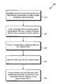
- FIG. 1shows a cross-sectional block diagram of a composite III-nitride chamber for in situ dopant implantation during growth of a III-nitride semiconductor body, according to one embodiment of the present invention.
- FIG. 2shows a flowchart presenting a method for enabling in situ dopant implantation during growth of a III-nitride semiconductor body, according to one embodiment of the present invention.
- FIG. 3shows a cross-sectional representation of a P-N junction formed in a III-nitride semiconductor body, according to one embodiment of the present invention.
- FIG. 4shows a cross-sectional representation of a III-nitride P-channel field-effect transistor (PFET), according to one embodiment of the present invention.
- FIG. 5shows a cross-sectional representation of a lateral diffusion III-nitride semiconductor device, according to one embodiment of the present invention.
- the present inventionis directed to in situ dopant implantation and growth of a III-nitride semiconductor body.
- the principles of the invention, as defined by the claims appended herein,can obviously be applied beyond the specifically described embodiments of the invention described herein.
- certain detailshave been left out in order to not obscure the inventive aspects of the invention. The details left out are within the knowledge of a person of ordinary skill in the art.
- the present inventorhas realized that selective doping of spatially defined regions within a III-nitride semiconductor body can be performed by dopant implantation without compromising the structure or stoichiometry of the III-nitride semiconductor material, when dopant implantation is performed in situ to a growth environment for the III-nitride semiconductor body.
- the present applicationdiscloses an approach that makes it possible to perform junction engineering in a III-nitride semiconductor body.
- the present inventive conceptsmay be applied to facilitate either N type or P type dopant implantation, the fabrication of P-channel devices, which is particularly problematic for the conventional art, is rendered significantly simpler and more economical to perform.
- FIG. 1shows a cross-sectional block diagram of composite III-nitride chamber 100 for in situ dopant implantation during growth of a III-nitride semiconductor body, according to one embodiment of the present invention.
- composite III-nitride chamber 100comprises growth chamber 110 , dopant implanter 130 , and transition chamber 120 including differential pressure cells 122 a , 122 b , and 122 c .
- support substrate 112to support growth of III-nitride semiconductor body 140 , such as a GaN body, for example.
- Support substrate 112may be selected from any suitable substrate material for the growth of a III-nitride semiconductor, and may include silicon, silicon carbide, sapphire, and when available, a native III-nitride semiconductor substrate, for example.
- growth chamber 110includes platform 106 , which may be a rotating platform, for example, on which support substrate 112 may be placed during growth and dopant implantation of III-nitride semiconductor body 140 .
- platform 106which may be a rotating platform, for example, on which support substrate 112 may be placed during growth and dopant implantation of III-nitride semiconductor body 140 .
- growth chamber 110is equipped with intake port 102 to allow for the entry of reactant gas, as well as output port 104 for the exit of reactant gas.
- growth chamber 110 of composite III-nitride chamber 100may also include Faraday cup 114 . When present, Faraday cup 114 may be linked to a voltage current meter (not shown in FIG. 1 ) through wires 108 a and 108 b , to measure the dosage of dopant ions being received from dopant implanter 130 .
- Dopant implanter 130provides dopant ions for implantation into III-nitride semiconductor body 140 along ion path 132 , and may perform selective implantation of portions of III-nitride semiconductor body 140 using a direct write type ion beam procedure, for example. In that embodiment, dopant implanter 130 may require a high vacuum environment. Such an environment is provided in composite III nitride chamber 110 by transition chamber 120 . In addition to providing a suitable environment for operation of dopant implanter 130 , transition chamber 120 also serves to interface dopant implanter 130 with growth chamber 110 , which may not be operating in a high vacuum state.
- transition chamber 120may include several differential pressure cells 122 a , 122 b , and 122 c .
- Each differential pressure cell 122 a , 122 b , and 122 cis in communication with an adjacent differential pressure cell through respective apertures 126 ab and 126 bc .
- ion path 132passes through apertures 126 bc and 126 ab to travel through transition chamber 120 , which interfaces dopant implanter 130 and growth chamber 110 through linking aperture 128 , through which ion path 132 also passes.
- each differential pressure cell 122 a , 122 b , and 122 cmay be evacuated using respective pumps 124 a , 124 b , and 124 c .
- Each of pumps 124 a , 124 b , and 124 cmay be in direct communication with the space enclosed by respective differential pressure cells 122 a , 122 b , and 122 c , as shown schematically in FIG. 1 .
- a composite III-nitride chamber according to the present embodimentmay further include a plurality of deflection plates, such as deflection plates 116 , positioned inside growth chamber 110 , on either side of linking aperture 128 .
- Deflection plates 116can be used to change the direction of travel of the dopant ions entering growth chamber 110 , for example. It is noted that that deflection plates 116 may be used to direct the dopant ions at Faraday cup 114 periodically, for instance, approximately 1% of the time, in order to measure the ion dosage being directed at III-nitride semiconductor body 140 , and in turn, to estimate the concentration of dopants implanted therein.
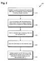
- exemplary composite III-nitride chamber 100will be further described by reference to flowchart 200 , in FIG. 2 , which describes the steps, according to one embodiment of the present invention, of a method for enabling in situ dopant implantation during growth of a III-nitride semiconductor body.
- flowchart 200describes the steps, according to one embodiment of the present invention, of a method for enabling in situ dopant implantation during growth of a III-nitride semiconductor body.
- flowchart 200describes the steps, according to one embodiment of the present invention, of a method for enabling in situ dopant implantation during growth of a III-nitride semiconductor body.
- step 210 of flowchart 200comprises establishing a growth environment for growing a GaN body, e.g., III-nitride semiconductor body 140 , in composite III-nitride chamber 100 including dopant implanter 130 .
- a GaN body 140e.g., III-nitride semiconductor body 140
- the present methodwill hereinafter refer to “GaN body 140 ,” rather than “III-nitride semiconductor body 140 .”
- GaN body 140may correspond to a body formed from any combination of suitable III-nitride semiconductor materials, as described in the definition section disclosed as part of the background of the present application.
- GaN body 140may comprise a first III-nitride semiconductor layer and a second III-nitride semiconductor layer formed over the first III nitride semiconductor layer, for example, wherein the second III-nitride semiconductor layer comprises a III-nitride semiconductor having a wider band gap than the III-nitride semiconductor forming the first III-nitride semiconductor layer.
- Step 210may be performed in composite III-nitride chamber 100 including dopant implanter 130 , through establishment of a suitable temperature and gas pressure for growth of the GaN body in growth chamber 110 .
- reactant gasmay be fed through intake port 102 , and thermal equilibrium may be established at a temperature greater than approximately eight hundred degrees Centigrade (800° C.).
- respective differential pressure cells 122 a , 122 b , and 122 cmay be evacuated until a suitable, high vacuum condition is obtained in the environment of transition chamber 120 .
- the pressure conditions in growth chamber 110 , as well as the configuration of transition chamber 120may depend on the type of growth that is being practiced.
- the pressure inside of growth chamber 110may be in the range of a few hundred millitor (mTorr).
- MBEmolecular-beam epitaxy
- the pressure inside growth chamber 110may be approximately 10 ⁇ 7 to 10 ⁇ 11 Torr, comparable to the high vacuum required by dopant implanter 130 .
- transition chamber 120having three differential pressure cells 122 a , 122 b , and 122 c to interface the different pressure environments required for respective dopant implanter 130 and growth chamber 110 , other embodiments corresponding to different pressure differentials may have more, or fewer, differential pressure cells. Moreover, where the growth environment and the environment required by dopant implanter 130 are comparable, for example, when growth proceeds by MBE, transition chamber 120 may be absent entirely, and dopant implanter 130 may interface growth chamber 110 directly, or even by included within growth chamber 110 .
- step 220 of flowchart 200comprises forming a nucleation film (not shown in FIG. 1 ) comprising silicon nitride and and/or aluminum nitride (AlN) over support substrate 112 placed in composite III-nitride chamber 100 .
- Step 220is typically a preliminary step to prepare support substrate 112 for growth of GaN body 140 .
- step 220is followed by step 230 , comprising forming a transition layer (also not shown in FIG. 1 ) comprising AlN over the nucleation film.
- the transition layer formed in step 230may itself correspond to a plurality of distinguishable layers mediating the lattice transition from support substrate 112 to GaN body 140 .
- the transition layermay include, for example, a series of aluminum gallium nitride (AlGaN) layers comprising progressively less aluminum and more gallium, until a suitable transition to GaN body 140 is achieved.
- AlGaNaluminum gallium nitride
- step 240comprises growing GaN body 140 over the transition layer formed in step 230 .
- step 240may be performed in growth chamber 110 of composite III nitride chamber 100 .
- Growth of GaN body 140may be performed by MOCVD or MBE, for example, and may proceed in a suitable atmospheric and thermal environment for growing GaN, such as in the presence of a nitrogen precursor gas like ammonia, additional reactant gases such as trimethylgallium (TMG) and trimethylaluminum (TMA), and at a temperature of greater than approximately 800° C., for instance.
- TMGtrimethylgallium
- TMAtrimethylaluminum
- GaN body 140may by grown as a doped GaN body, such as an N type or a P type GaN body, for example.
- GaN body 140may be grown undoped, in which case GaN body 140 will have a nominal N type conductivity due to the presence of lattice defects formed during the growth process, as known in the art.
- step 250 of flowchart 200comprises implanting dopant ions into GaN body 140 while maintaining the growth environment in composite III-nitride chamber 100 at over approximately 800° C.
- Step 250may be performed by dopant implanter 130 in combination with growth chamber 110 , and may result in any desired species being implanted into GaN body 140 .
- N type dopantssuch as silicon (Si)
- P type dopantssuch as magnesium (Mg) may be implanted, for example.
- GaN body 140is grown undoped, for example, N type doping and P type doping may both be performed, resulting in laterally adjacent regions of GaN body 140 having opposite conductivity types.
- relatively low energy surface implantation of GaN body 140may be preferred, utilizing implantation energies of less than approximately 100 keV, for example, from 10 to 100 keV. In other embodiments, however, deeper penetration into GaN body 140 may be desired, so that implantation energies of more than one MeV may be employed. Thus implantation may be performed using a broad range of implantation energies, from approximately 10 keV to more than 1000 keV.
- the ion beam used for dopant implantationcan be as wide as 1/10 microns wide, for example.
- relatively low implantation energiesare used in order to implant the dopants near the surface during the growth process, for example, to a depth of approximately fifty to approximately 200 angstroms (50-200 ⁇ ) in GaN body 140 .
- relatively high implantation energiesmay be utilized to form deeply placed spatially defined doped islands in GaN body 140 .
- GaN body 140can be doped to any concentration, for example, GaN body 140 can be doped with an ion dose in the range of approximately 10 12 /cm 2 to 10 16 /cm 2 .
- dopant implantation and growth of GaN body 140may occur substantially concurrently. In other embodiments, however, the two processes may alternate in a cyclical fashion, so that growth and dopant implantation of GaN body 140 proceeds through an iterative set of growth steps and dopant implantation steps performed in situ.
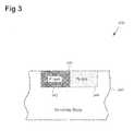
- FIGS. 3 , 4 , and 5show respective III-nitride semiconductor structures formed according to the principles described in the present application. Each of the structures is representative of the advantages associated with enablement of spatially defined selective doping of a III-nitride body, and the variety of junction engineering techniques that are facilitated by the present approach.
- FIG. 3shows a cross-sectional representation of a P-N junction formed in a III-nitride semiconductor body, according to one embodiment of the present invention.
- Structure 300in FIG. 3 , includes P type doped region 342 and N type doped region 344 formed in III-nitride semiconductor body 340 .
- III-nitride semiconductor body 340corresponds to III-nitride semiconductor body 140 , shown in FIG. 1 , and may be a GaN body, for example.
- both of P type doped region 342 and N type doped region 344are spatially defined within III-nitride semiconductor body 340 , and have been selectively formed so as to be laterally adjacent one another.
- Structure 300may be utilized in the implementation of a diode, for example, or as a base for a bipolar junction transistor fabricated in III-nitride body 340 .
- FIG. 4shows a cross-sectional representation of a III-nitride P-channel field-effect transistor (PFET), according to one embodiment of the present invention.
- Structure 400in FIG. 4 , includes gate structure 449 , as well as P type doped source region 447 and P type doped drain region 448 formed in N type III-nitride semiconductor body 440 .
- III-nitride semiconductor body 440corresponds to III-nitride semiconductor body 140 , shown in FIG. 1 , and may be a GaN body, for example. As shown in FIG.
- both of respective P type source and drain regions 447 and 448include deeply implanted portions and shallower extension regions, and give some indication of the degree of spatial selectivity that may be achieved using the present inventive concepts.
- structure 400shows formation of P type doped regions through selective spatially defined implantation of III-nitride body 440 , which as is well known in the art, is highly impracticable using conventional approaches.
- FIG. 5shows a cross-sectional representation of a lateral diffusion III-nitride semiconductor device, according to one embodiment of the present invention.
- Structure 500in FIG. 5 , includes gate structure 549 , P type doped region 542 , and N type doped regions 547 and 548 formed in III-nitride semiconductor body 540 .
- III-nitride semiconductor body 540corresponds to III-nitride semiconductor body 140 , shown in FIG. 1 , and may be a GaN body, for example.
- N type doped region 547which may serve as a source region, is formed within P type doped region 542 formed in III nitride semiconductor body 540 .
- gate structure 549may include a gate insulator layer, such as a silicon nitride layer, for example.
- structure 500may correspond to fabrication of a lateral diffusion MISFET in III-nitride, analogous to a laterally diffused metal oxide semiconductor (LDMOS) transistor conventionally formed in silicon.
- LDMOSlaterally diffused metal oxide semiconductor
- the disclosed novel conceptsenable laterally selective doping of a III-nitride semiconductor body, while concurrently maintaining the structural and stoichiometric properties of the semiconductor material.
- the present applicationdiscloses an approach that makes it possible to advantageously perform junction engineering in a III-nitride semiconductor body.
- the present inventive conceptsmay be applied to facilitate either N type or P type dopant implantation, the fabrication of P-channel devices is rendered significantly easier to achieve.
Landscapes
- Engineering & Computer Science (AREA)
- Chemical & Material Sciences (AREA)
- Physics & Mathematics (AREA)
- Microelectronics & Electronic Packaging (AREA)
- Manufacturing & Machinery (AREA)
- Computer Hardware Design (AREA)
- Metallurgy (AREA)
- Power Engineering (AREA)
- General Physics & Mathematics (AREA)
- Organic Chemistry (AREA)
- Condensed Matter Physics & Semiconductors (AREA)
- Crystallography & Structural Chemistry (AREA)
- Materials Engineering (AREA)
- General Chemical & Material Sciences (AREA)
- Chemical Kinetics & Catalysis (AREA)
- Inorganic Chemistry (AREA)
- High Energy & Nuclear Physics (AREA)
- Analytical Chemistry (AREA)
- Health & Medical Sciences (AREA)
- Toxicology (AREA)
- Insulated Gate Type Field-Effect Transistor (AREA)
- Recrystallisation Techniques (AREA)
- Crystals, And After-Treatments Of Crystals (AREA)
Abstract
Description
Claims (20)
Priority Applications (3)
| Application Number | Priority Date | Filing Date | Title |
|---|---|---|---|
| US12/661,342US8093597B2 (en) | 2007-06-25 | 2010-03-16 | In situ dopant implantation and growth of a III-nitride semiconductor body |
| EP11001199AEP2369040A1 (en) | 2010-03-16 | 2011-02-15 | In situ dopant implantation and growth of a III-nitride semiconductor body |
| JP2011050366AJP2011192993A (en) | 2010-03-16 | 2011-03-08 | In situ dopant implantation and growth of iii-nitride semiconductor body |
Applications Claiming Priority (3)
| Application Number | Priority Date | Filing Date | Title |
|---|---|---|---|
| US93710107P | 2007-06-25 | 2007-06-25 | |
| US12/006,562US8395132B2 (en) | 2007-06-25 | 2008-01-03 | Ion implanting while growing a III-nitride layer |
| US12/661,342US8093597B2 (en) | 2007-06-25 | 2010-03-16 | In situ dopant implantation and growth of a III-nitride semiconductor body |
Related Parent Applications (1)
| Application Number | Title | Priority Date | Filing Date |
|---|---|---|---|
| US12/006,562Continuation-In-PartUS8395132B2 (en) | 2007-06-25 | 2008-01-03 | Ion implanting while growing a III-nitride layer |
Publications (2)
| Publication Number | Publication Date |
|---|---|
| US20100171126A1 US20100171126A1 (en) | 2010-07-08 |
| US8093597B2true US8093597B2 (en) | 2012-01-10 |
Family
ID=44121457
Family Applications (1)
| Application Number | Title | Priority Date | Filing Date |
|---|---|---|---|
| US12/661,342Expired - Fee RelatedUS8093597B2 (en) | 2007-06-25 | 2010-03-16 | In situ dopant implantation and growth of a III-nitride semiconductor body |
Country Status (3)
| Country | Link |
|---|---|
| US (1) | US8093597B2 (en) |
| EP (1) | EP2369040A1 (en) |
| JP (1) | JP2011192993A (en) |
Cited By (6)
| Publication number | Priority date | Publication date | Assignee | Title |
|---|---|---|---|---|
| US20110210338A1 (en)* | 2010-03-01 | 2011-09-01 | International Rectifier Corporation | Efficient High Voltage Switching Circuits and Monolithic Integration of Same |
| US20110210337A1 (en)* | 2010-03-01 | 2011-09-01 | International Rectifier Corporation | Monolithic integration of silicon and group III-V devices |
| US20140213046A1 (en)* | 2007-06-25 | 2014-07-31 | International Rectifier Corporation | Fabrication of III-Nitride Layers |
| US9218991B2 (en) | 2007-06-25 | 2015-12-22 | Infineon Technologies Americas Corp. | Ion implantation at high temperature surface equilibrium conditions |
| CN105518861A (en)* | 2013-06-20 | 2016-04-20 | 斯坦舍有限公司 | Gate-controlled Charge Modulation Devices for CMOS Sensors |
| US10109763B2 (en) | 2016-03-10 | 2018-10-23 | Samsung Electronics Co., Ltd. | Light-emitting devices and methods of manufacturing the same |
Families Citing this family (6)
| Publication number | Priority date | Publication date | Assignee | Title |
|---|---|---|---|---|
| EP2765596B1 (en)* | 2013-02-12 | 2018-07-11 | Infineon Technologies Americas Corp. | Ion implantation at high temperature surface equilibrium conditions |
| US9123828B2 (en) | 2013-11-14 | 2015-09-01 | Infineon Technologies Ag | Semiconductor device and method for forming a semiconductor device |
| FR3026558B1 (en) | 2014-09-26 | 2018-03-09 | Commissariat A L'energie Atomique Et Aux Energies Alternatives | METHOD FOR ACTIVATING DOPANTS IN A SEMICONDUCTOR LAYER BASED ON GAN |
| FR3026557B1 (en) | 2014-09-26 | 2018-03-16 | Commissariat A L'energie Atomique Et Aux Energies Alternatives | METHOD FOR DOPING A SEMICONDUCTOR BASED ON GAN |
| FR3026556A1 (en) | 2014-09-26 | 2016-04-01 | Commissariat Energie Atomique | PROCESS FOR PRODUCING A SEMICONDUCTOR LAYER BASED ON GAN IMPROVED |
| FR3026555A1 (en) | 2014-09-26 | 2016-04-01 | Commissariat Energie Atomique | METHOD FOR ACTIVATING DOPANTS IN A GAN SEMICONDUCTOR LAYER THROUGH IMPLANTATIONS AND SUCCESSIVE THERMAL TREATMENTS |
Citations (15)
| Publication number | Priority date | Publication date | Assignee | Title |
|---|---|---|---|---|
| US4831270A (en) | 1987-05-21 | 1989-05-16 | Ion Implant Services | Ion implantation apparatus |
| US5354584A (en)* | 1991-08-08 | 1994-10-11 | Schmidt Instruments, Inc. | In situ low energy ion doping of materials grown by CVD |
| US5374318A (en) | 1987-06-25 | 1994-12-20 | University Of Houston | Process for the deposition of diamond films using low energy, mass-selected ion beam deposition |
| US5789265A (en)* | 1995-08-31 | 1998-08-04 | Kabushiki Kaisha Toshiba | Method of manufacturing blue light-emitting device by using BCL3 and CL2 |
| WO1998056046A1 (en) | 1997-06-06 | 1998-12-10 | Centrum Badan Wysokocisnieniowych Polskiej Akademii Nauk | THE METHOD OF FABRICATION OF SEMICONDUCTING COMPOUNDS OF NITRIDES A3B5 OF p- AND n-TYPE ELECTRIC CONDUCTIVITY |
| US5932882A (en)* | 1995-11-08 | 1999-08-03 | Applied Materials, Inc. | Ion implanter with post mass selection deceleration |
| US5981393A (en) | 1997-09-29 | 1999-11-09 | Cyntec Co., Ltd. | Method of forming electrodes at the end surfaces of chip array resistors |
| US6123768A (en) | 1991-03-18 | 2000-09-26 | The Trustees Of Boston University | Method for the preparation and doping of highly insulating monocrystalline gallium nitride thin films |
| US20010029086A1 (en)* | 2000-02-24 | 2001-10-11 | Masahiro Ogawa | Semiconductor device, method for fabricating the same and method for fabricating semiconductor substrate |
| US20010032999A1 (en) | 2000-04-25 | 2001-10-25 | Seikoh Yoshida | GaN-based compound semiconductor device |
| US20040041169A1 (en)* | 2002-08-26 | 2004-03-04 | Fan Ren | GaN-type enhancement MOSFET using hetero structure |
| US20040207029A1 (en) | 2002-07-16 | 2004-10-21 | Braddock Walter David | Junction field effect metal oxide compound semiconductor integrated transistor devices |
| US20050191828A1 (en) | 2000-08-11 | 2005-09-01 | Applied Materials, Inc. | Method for ion implanting insulator material to reduce dielectric constant |
| US20060261352A1 (en) | 2001-03-27 | 2006-11-23 | Takashi Takahashi | Semiconductor light-emitting device, surface-emission laser diode, and production apparatus thereof, production method, optical module and optical telecommunication system |
| US20080315129A1 (en) | 2007-06-25 | 2008-12-25 | International Rectifier Corporation | Ion planting while growing a III-nitride layer |
Family Cites Families (2)
| Publication number | Priority date | Publication date | Assignee | Title |
|---|---|---|---|---|
| NL8700246A (en)* | 1987-02-02 | 1988-09-01 | Stichting Waterbouwkundig Lab | METHOD AND APPARATUS FOR INSULATING, TREATING AND / OR REMOVING IN CELLS HIGHLY CONTAMINATED MATERIAL IN OR ON THE SOIL. |
| JP4477191B2 (en)* | 2000-04-25 | 2010-06-09 | 古河電気工業株式会社 | Insulated gate semiconductor device |
- 2010
- 2010-03-16USUS12/661,342patent/US8093597B2/ennot_activeExpired - Fee Related
- 2011
- 2011-02-15EPEP11001199Apatent/EP2369040A1/ennot_activeWithdrawn
- 2011-03-08JPJP2011050366Apatent/JP2011192993A/enactivePending
Patent Citations (15)
| Publication number | Priority date | Publication date | Assignee | Title |
|---|---|---|---|---|
| US4831270A (en) | 1987-05-21 | 1989-05-16 | Ion Implant Services | Ion implantation apparatus |
| US5374318A (en) | 1987-06-25 | 1994-12-20 | University Of Houston | Process for the deposition of diamond films using low energy, mass-selected ion beam deposition |
| US6123768A (en) | 1991-03-18 | 2000-09-26 | The Trustees Of Boston University | Method for the preparation and doping of highly insulating monocrystalline gallium nitride thin films |
| US5354584A (en)* | 1991-08-08 | 1994-10-11 | Schmidt Instruments, Inc. | In situ low energy ion doping of materials grown by CVD |
| US5789265A (en)* | 1995-08-31 | 1998-08-04 | Kabushiki Kaisha Toshiba | Method of manufacturing blue light-emitting device by using BCL3 and CL2 |
| US5932882A (en)* | 1995-11-08 | 1999-08-03 | Applied Materials, Inc. | Ion implanter with post mass selection deceleration |
| WO1998056046A1 (en) | 1997-06-06 | 1998-12-10 | Centrum Badan Wysokocisnieniowych Polskiej Akademii Nauk | THE METHOD OF FABRICATION OF SEMICONDUCTING COMPOUNDS OF NITRIDES A3B5 OF p- AND n-TYPE ELECTRIC CONDUCTIVITY |
| US5981393A (en) | 1997-09-29 | 1999-11-09 | Cyntec Co., Ltd. | Method of forming electrodes at the end surfaces of chip array resistors |
| US20010029086A1 (en)* | 2000-02-24 | 2001-10-11 | Masahiro Ogawa | Semiconductor device, method for fabricating the same and method for fabricating semiconductor substrate |
| US20010032999A1 (en) | 2000-04-25 | 2001-10-25 | Seikoh Yoshida | GaN-based compound semiconductor device |
| US20050191828A1 (en) | 2000-08-11 | 2005-09-01 | Applied Materials, Inc. | Method for ion implanting insulator material to reduce dielectric constant |
| US20060261352A1 (en) | 2001-03-27 | 2006-11-23 | Takashi Takahashi | Semiconductor light-emitting device, surface-emission laser diode, and production apparatus thereof, production method, optical module and optical telecommunication system |
| US20040207029A1 (en) | 2002-07-16 | 2004-10-21 | Braddock Walter David | Junction field effect metal oxide compound semiconductor integrated transistor devices |
| US20040041169A1 (en)* | 2002-08-26 | 2004-03-04 | Fan Ren | GaN-type enhancement MOSFET using hetero structure |
| US20080315129A1 (en) | 2007-06-25 | 2008-12-25 | International Rectifier Corporation | Ion planting while growing a III-nitride layer |
Non-Patent Citations (3)
| Title |
|---|
| Hashimoto et al. ("Focused ion beam doping for GaAs MBE growth", Microelectronic Engineering, 4, pp. 181-193, 1986).* |
| Rubin et al. ("P-type gallium nitride by reactive ion-beam molecular beam epitaxy with ion implantation, diffusion or coevaporation of Mg", Applied Physics Letters, (1), pp. 64-66, 1994).* |
| Sazio et al. ("Fabrication of in Situ Ohmic Contacts Patterned in Three Dimensions using Focused Ion Beam During Molecular Beam Epitaxial Growth", J. Vac. Sci. Technol. B 15(6), pp. 2337-2341).* |
Cited By (10)
| Publication number | Priority date | Publication date | Assignee | Title |
|---|---|---|---|---|
| US20140213046A1 (en)* | 2007-06-25 | 2014-07-31 | International Rectifier Corporation | Fabrication of III-Nitride Layers |
| US9202687B2 (en)* | 2007-06-25 | 2015-12-01 | Infineon Technologies Americas Corp. | Fabrication of III-nitride layers |
| US9218991B2 (en) | 2007-06-25 | 2015-12-22 | Infineon Technologies Americas Corp. | Ion implantation at high temperature surface equilibrium conditions |
| US20110210338A1 (en)* | 2010-03-01 | 2011-09-01 | International Rectifier Corporation | Efficient High Voltage Switching Circuits and Monolithic Integration of Same |
| US20110210337A1 (en)* | 2010-03-01 | 2011-09-01 | International Rectifier Corporation | Monolithic integration of silicon and group III-V devices |
| US8981380B2 (en)* | 2010-03-01 | 2015-03-17 | International Rectifier Corporation | Monolithic integration of silicon and group III-V devices |
| US9219058B2 (en) | 2010-03-01 | 2015-12-22 | Infineon Technologies Americas Corp. | Efficient high voltage switching circuits and monolithic integration of same |
| CN105518861A (en)* | 2013-06-20 | 2016-04-20 | 斯坦舍有限公司 | Gate-controlled Charge Modulation Devices for CMOS Sensors |
| CN105518861B (en)* | 2013-06-20 | 2018-10-02 | 斯坦舍有限公司 | Gate controlled charge modulation device for cmos sensor |
| US10109763B2 (en) | 2016-03-10 | 2018-10-23 | Samsung Electronics Co., Ltd. | Light-emitting devices and methods of manufacturing the same |
Also Published As
| Publication number | Publication date |
|---|---|
| US20100171126A1 (en) | 2010-07-08 |
| JP2011192993A (en) | 2011-09-29 |
| EP2369040A1 (en) | 2011-09-28 |
Similar Documents
| Publication | Publication Date | Title |
|---|---|---|
| US8093597B2 (en) | In situ dopant implantation and growth of a III-nitride semiconductor body | |
| CN101611473B (en) | Methods of fabricating semiconductor devices including implanted regions for providing low-resistance contact to buried layers and related devices | |
| JP5295496B2 (en) | Semiconductor device including implantation region and protective layer and method of forming the same | |
| EP3501033B1 (en) | Semiconductor material growth of a high resistivity nitride buffer layer using ion implantation | |
| US20230326996A1 (en) | Gallium nitride-based high electron mobility transistor epitaxial wafer and preparation method therefor | |
| JP6882503B2 (en) | Gallium Nitride High Electron Mobility Transistor with High Breakdown Voltage and Its Formation Method | |
| KR20040104959A (en) | Doped Group III-V Nitride Material, And Microelectronic Device And Device Precursor Structures Comprising Same | |
| CN108140561A (en) | The manufacturing method of epitaxial substrate for semiconductor device, semiconductor element and epitaxial substrate for semiconductor device | |
| JP2018528614A (en) | Reduction of parasitic channels in III-nitride semiconductor structures | |
| US20240021719A1 (en) | Semiconductor device having doped seed layer and method of manufacturing the same | |
| US20160079370A1 (en) | Semiconductor device, semiconductor wafer, and semiconductor device manufacturing method | |
| US10134908B2 (en) | Semiconductor device and manufacturing method thereof | |
| US8901609B1 (en) | Transistor having doped substrate and method of making the same | |
| WO2018098952A1 (en) | Gan-based epitaxial structure, semiconductor device and formation method therefor | |
| CN106972058A (en) | A kind of semiconductor devices and preparation method thereof | |
| US20230121332A1 (en) | Radio frequency devices, silicon carbide homoepitaxial substrates and manufacturing methods thereof | |
| JP2009094337A (en) | Manufacturing method of semiconductor device | |
| US8841179B2 (en) | Nitride semiconductor device using selective growth and manufacturing method thereof | |
| JP5746927B2 (en) | Semiconductor substrate, semiconductor device, and method of manufacturing semiconductor substrate | |
| KR101038836B1 (en) | Nitride type heterojunction field effect transistor manufacturing method | |
| JP6416705B2 (en) | Field effect transistor and manufacturing method thereof | |
| JP2000068497A (en) | GaN-based compound semiconductor device | |
| US10490408B2 (en) | Method for manufacturing semiconductor device | |
| US20200194580A1 (en) | Nitride semiconductor substrate and nitride semiconductor device | |
| US9218991B2 (en) | Ion implantation at high temperature surface equilibrium conditions |
Legal Events
| Date | Code | Title | Description |
|---|---|---|---|
| AS | Assignment | Owner name:INTERNATIONAL RECTIFIER CORPORATION, CALIFORNIA Free format text:ASSIGNMENT OF ASSIGNORS INTEREST;ASSIGNOR:BRIERE, MICHAEL A.;REEL/FRAME:025590/0381 Effective date:20071220 | |
| ZAAA | Notice of allowance and fees due | Free format text:ORIGINAL CODE: NOA | |
| ZAAB | Notice of allowance mailed | Free format text:ORIGINAL CODE: MN/=. | |
| STCF | Information on status: patent grant | Free format text:PATENTED CASE | |
| FPAY | Fee payment | Year of fee payment:4 | |
| AS | Assignment | Owner name:INFINEON TECHNOLOGIES AMERICAS CORP., CALIFORNIA Free format text:CHANGE OF NAME;ASSIGNOR:INTERNATIONAL RECTIFIER CORPORATION;REEL/FRAME:046612/0968 Effective date:20151001 | |
| MAFP | Maintenance fee payment | Free format text:PAYMENT OF MAINTENANCE FEE, 8TH YEAR, LARGE ENTITY (ORIGINAL EVENT CODE: M1552); ENTITY STATUS OF PATENT OWNER: LARGE ENTITY Year of fee payment:8 | |
| FEPP | Fee payment procedure | Free format text:MAINTENANCE FEE REMINDER MAILED (ORIGINAL EVENT CODE: REM.); ENTITY STATUS OF PATENT OWNER: LARGE ENTITY | |
| LAPS | Lapse for failure to pay maintenance fees | Free format text:PATENT EXPIRED FOR FAILURE TO PAY MAINTENANCE FEES (ORIGINAL EVENT CODE: EXP.); ENTITY STATUS OF PATENT OWNER: LARGE ENTITY | |
| STCH | Information on status: patent discontinuation | Free format text:PATENT EXPIRED DUE TO NONPAYMENT OF MAINTENANCE FEES UNDER 37 CFR 1.362 | |
| FP | Lapsed due to failure to pay maintenance fee | Effective date:20240110 |