US8092068B2 - Light redirecting films and film systems - Google Patents
Light redirecting films and film systemsDownload PDFInfo
- Publication number
- US8092068B2 US8092068B2US12/364,554US36455409AUS8092068B2US 8092068 B2US8092068 B2US 8092068B2US 36455409 AUS36455409 AUS 36455409AUS 8092068 B2US8092068 B2US 8092068B2
- Authority
- US
- United States
- Prior art keywords
- light
- optical
- optical elements
- pattern
- optical assembly
- Prior art date
- Legal status (The legal status is an assumption and is not a legal conclusion. Google has not performed a legal analysis and makes no representation as to the accuracy of the status listed.)
- Expired - Fee Related, expires
Links
Images


Classifications
- F—MECHANICAL ENGINEERING; LIGHTING; HEATING; WEAPONS; BLASTING
- F21—LIGHTING
- F21V—FUNCTIONAL FEATURES OR DETAILS OF LIGHTING DEVICES OR SYSTEMS THEREOF; STRUCTURAL COMBINATIONS OF LIGHTING DEVICES WITH OTHER ARTICLES, NOT OTHERWISE PROVIDED FOR
- F21V5/00—Refractors for light sources
- A—HUMAN NECESSITIES
- A61—MEDICAL OR VETERINARY SCIENCE; HYGIENE
- A61M—DEVICES FOR INTRODUCING MEDIA INTO, OR ONTO, THE BODY; DEVICES FOR TRANSDUCING BODY MEDIA OR FOR TAKING MEDIA FROM THE BODY; DEVICES FOR PRODUCING OR ENDING SLEEP OR STUPOR
- A61M21/00—Other devices or methods to cause a change in the state of consciousness; Devices for producing or ending sleep by mechanical, optical, or acoustical means, e.g. for hypnosis
- A61M21/02—Other devices or methods to cause a change in the state of consciousness; Devices for producing or ending sleep by mechanical, optical, or acoustical means, e.g. for hypnosis for inducing sleep or relaxation, e.g. by direct nerve stimulation, hypnosis, analgesia
- F—MECHANICAL ENGINEERING; LIGHTING; HEATING; WEAPONS; BLASTING
- F21—LIGHTING
- F21V—FUNCTIONAL FEATURES OR DETAILS OF LIGHTING DEVICES OR SYSTEMS THEREOF; STRUCTURAL COMBINATIONS OF LIGHTING DEVICES WITH OTHER ARTICLES, NOT OTHERWISE PROVIDED FOR
- F21V11/00—Screens not covered by groups F21V1/00, F21V3/00, F21V7/00 or F21V9/00
- F—MECHANICAL ENGINEERING; LIGHTING; HEATING; WEAPONS; BLASTING
- F21—LIGHTING
- F21V—FUNCTIONAL FEATURES OR DETAILS OF LIGHTING DEVICES OR SYSTEMS THEREOF; STRUCTURAL COMBINATIONS OF LIGHTING DEVICES WITH OTHER ARTICLES, NOT OTHERWISE PROVIDED FOR
- F21V5/00—Refractors for light sources
- F21V5/10—Refractors for light sources comprising photoluminescent material
- G—PHYSICS
- G02—OPTICS
- G02B—OPTICAL ELEMENTS, SYSTEMS OR APPARATUS
- G02B6/00—Light guides; Structural details of arrangements comprising light guides and other optical elements, e.g. couplings
- G02B6/0001—Light guides; Structural details of arrangements comprising light guides and other optical elements, e.g. couplings specially adapted for lighting devices or systems
- G02B6/0011—Light guides; Structural details of arrangements comprising light guides and other optical elements, e.g. couplings specially adapted for lighting devices or systems the light guides being planar or of plate-like form
- G02B6/0013—Means for improving the coupling-in of light from the light source into the light guide
- G02B6/0015—Means for improving the coupling-in of light from the light source into the light guide provided on the surface of the light guide or in the bulk of it
- G02B6/0018—Redirecting means on the surface of the light guide
- G—PHYSICS
- G02—OPTICS
- G02B—OPTICAL ELEMENTS, SYSTEMS OR APPARATUS
- G02B6/00—Light guides; Structural details of arrangements comprising light guides and other optical elements, e.g. couplings
- G02B6/0001—Light guides; Structural details of arrangements comprising light guides and other optical elements, e.g. couplings specially adapted for lighting devices or systems
- G02B6/0011—Light guides; Structural details of arrangements comprising light guides and other optical elements, e.g. couplings specially adapted for lighting devices or systems the light guides being planar or of plate-like form
- G02B6/0013—Means for improving the coupling-in of light from the light source into the light guide
- G02B6/0015—Means for improving the coupling-in of light from the light source into the light guide provided on the surface of the light guide or in the bulk of it
- G02B6/002—Means for improving the coupling-in of light from the light source into the light guide provided on the surface of the light guide or in the bulk of it by shaping at least a portion of the light guide, e.g. with collimating, focussing or diverging surfaces
- G02B6/0021—Means for improving the coupling-in of light from the light source into the light guide provided on the surface of the light guide or in the bulk of it by shaping at least a portion of the light guide, e.g. with collimating, focussing or diverging surfaces for housing at least a part of the light source, e.g. by forming holes or recesses
- G—PHYSICS
- G02—OPTICS
- G02B—OPTICAL ELEMENTS, SYSTEMS OR APPARATUS
- G02B6/00—Light guides; Structural details of arrangements comprising light guides and other optical elements, e.g. couplings
- G02B6/0001—Light guides; Structural details of arrangements comprising light guides and other optical elements, e.g. couplings specially adapted for lighting devices or systems
- G02B6/0011—Light guides; Structural details of arrangements comprising light guides and other optical elements, e.g. couplings specially adapted for lighting devices or systems the light guides being planar or of plate-like form
- G02B6/0033—Means for improving the coupling-out of light from the light guide
- G02B6/0035—Means for improving the coupling-out of light from the light guide provided on the surface of the light guide or in the bulk of it
- G02B6/0036—2-D arrangement of prisms, protrusions, indentations or roughened surfaces
- G—PHYSICS
- G02—OPTICS
- G02B—OPTICAL ELEMENTS, SYSTEMS OR APPARATUS
- G02B6/00—Light guides; Structural details of arrangements comprising light guides and other optical elements, e.g. couplings
- G02B6/0001—Light guides; Structural details of arrangements comprising light guides and other optical elements, e.g. couplings specially adapted for lighting devices or systems
- G02B6/0011—Light guides; Structural details of arrangements comprising light guides and other optical elements, e.g. couplings specially adapted for lighting devices or systems the light guides being planar or of plate-like form
- G02B6/0033—Means for improving the coupling-out of light from the light guide
- G02B6/0035—Means for improving the coupling-out of light from the light guide provided on the surface of the light guide or in the bulk of it
- G02B6/0038—Linear indentations or grooves, e.g. arc-shaped grooves or meandering grooves, extending over the full length or width of the light guide
- G—PHYSICS
- G02—OPTICS
- G02B—OPTICAL ELEMENTS, SYSTEMS OR APPARATUS
- G02B6/00—Light guides; Structural details of arrangements comprising light guides and other optical elements, e.g. couplings
- G02B6/0001—Light guides; Structural details of arrangements comprising light guides and other optical elements, e.g. couplings specially adapted for lighting devices or systems
- G02B6/0011—Light guides; Structural details of arrangements comprising light guides and other optical elements, e.g. couplings specially adapted for lighting devices or systems the light guides being planar or of plate-like form
- G02B6/0033—Means for improving the coupling-out of light from the light guide
- G02B6/005—Means for improving the coupling-out of light from the light guide provided by one optical element, or plurality thereof, placed on the light output side of the light guide
- G02B6/0053—Prismatic sheet or layer; Brightness enhancement element, sheet or layer
- G—PHYSICS
- G02—OPTICS
- G02B—OPTICAL ELEMENTS, SYSTEMS OR APPARATUS
- G02B6/00—Light guides; Structural details of arrangements comprising light guides and other optical elements, e.g. couplings
- G02B6/0001—Light guides; Structural details of arrangements comprising light guides and other optical elements, e.g. couplings specially adapted for lighting devices or systems
- G02B6/0011—Light guides; Structural details of arrangements comprising light guides and other optical elements, e.g. couplings specially adapted for lighting devices or systems the light guides being planar or of plate-like form
- G02B6/0033—Means for improving the coupling-out of light from the light guide
- G02B6/0058—Means for improving the coupling-out of light from the light guide varying in density, size, shape or depth along the light guide
- G02B6/0061—Means for improving the coupling-out of light from the light guide varying in density, size, shape or depth along the light guide to provide homogeneous light output intensity
- G—PHYSICS
- G02—OPTICS
- G02B—OPTICAL ELEMENTS, SYSTEMS OR APPARATUS
- G02B6/00—Light guides; Structural details of arrangements comprising light guides and other optical elements, e.g. couplings
- G02B6/0001—Light guides; Structural details of arrangements comprising light guides and other optical elements, e.g. couplings specially adapted for lighting devices or systems
- G02B6/0011—Light guides; Structural details of arrangements comprising light guides and other optical elements, e.g. couplings specially adapted for lighting devices or systems the light guides being planar or of plate-like form
- G02B6/0065—Manufacturing aspects; Material aspects
- G—PHYSICS
- G02—OPTICS
- G02B—OPTICAL ELEMENTS, SYSTEMS OR APPARATUS
- G02B6/00—Light guides; Structural details of arrangements comprising light guides and other optical elements, e.g. couplings
- G02B6/0001—Light guides; Structural details of arrangements comprising light guides and other optical elements, e.g. couplings specially adapted for lighting devices or systems
- G02B6/0011—Light guides; Structural details of arrangements comprising light guides and other optical elements, e.g. couplings specially adapted for lighting devices or systems the light guides being planar or of plate-like form
- G02B6/0066—Light guides; Structural details of arrangements comprising light guides and other optical elements, e.g. couplings specially adapted for lighting devices or systems the light guides being planar or of plate-like form characterised by the light source being coupled to the light guide
- G02B6/0068—Arrangements of plural sources, e.g. multi-colour light sources
- A—HUMAN NECESSITIES
- A61—MEDICAL OR VETERINARY SCIENCE; HYGIENE
- A61B—DIAGNOSIS; SURGERY; IDENTIFICATION
- A61B90/00—Instruments, implements or accessories specially adapted for surgery or diagnosis and not covered by any of the groups A61B1/00 - A61B50/00, e.g. for luxation treatment or for protecting wound edges
- A61B90/30—Devices for illuminating a surgical field, the devices having an interrelation with other surgical devices or with a surgical procedure
- A61B2090/309—Devices for illuminating a surgical field, the devices having an interrelation with other surgical devices or with a surgical procedure using white LEDs
- A—HUMAN NECESSITIES
- A61—MEDICAL OR VETERINARY SCIENCE; HYGIENE
- A61M—DEVICES FOR INTRODUCING MEDIA INTO, OR ONTO, THE BODY; DEVICES FOR TRANSDUCING BODY MEDIA OR FOR TAKING MEDIA FROM THE BODY; DEVICES FOR PRODUCING OR ENDING SLEEP OR STUPOR
- A61M21/00—Other devices or methods to cause a change in the state of consciousness; Devices for producing or ending sleep by mechanical, optical, or acoustical means, e.g. for hypnosis
- A61M2021/0005—Other devices or methods to cause a change in the state of consciousness; Devices for producing or ending sleep by mechanical, optical, or acoustical means, e.g. for hypnosis by the use of a particular sense, or stimulus
- A61M2021/0044—Other devices or methods to cause a change in the state of consciousness; Devices for producing or ending sleep by mechanical, optical, or acoustical means, e.g. for hypnosis by the use of a particular sense, or stimulus by the sight sense
- A—HUMAN NECESSITIES
- A61—MEDICAL OR VETERINARY SCIENCE; HYGIENE
- A61N—ELECTROTHERAPY; MAGNETOTHERAPY; RADIATION THERAPY; ULTRASOUND THERAPY
- A61N5/00—Radiation therapy
- A61N5/06—Radiation therapy using light
- A61N2005/063—Radiation therapy using light comprising light transmitting means, e.g. optical fibres
- A—HUMAN NECESSITIES
- A61—MEDICAL OR VETERINARY SCIENCE; HYGIENE
- A61N—ELECTROTHERAPY; MAGNETOTHERAPY; RADIATION THERAPY; ULTRASOUND THERAPY
- A61N5/00—Radiation therapy
- A61N5/06—Radiation therapy using light
- A61N2005/065—Light sources therefor
- A61N2005/0651—Diodes
- A61N2005/0652—Arrays of diodes
- A—HUMAN NECESSITIES
- A61—MEDICAL OR VETERINARY SCIENCE; HYGIENE
- A61N—ELECTROTHERAPY; MAGNETOTHERAPY; RADIATION THERAPY; ULTRASOUND THERAPY
- A61N5/00—Radiation therapy
- A61N5/06—Radiation therapy using light
- A61N5/0613—Apparatus adapted for a specific treatment
- A61N5/0621—Hyperbilirubinemia, jaundice treatment
- G—PHYSICS
- G02—OPTICS
- G02B—OPTICAL ELEMENTS, SYSTEMS OR APPARATUS
- G02B6/00—Light guides; Structural details of arrangements comprising light guides and other optical elements, e.g. couplings
- G02B6/0001—Light guides; Structural details of arrangements comprising light guides and other optical elements, e.g. couplings specially adapted for lighting devices or systems
- G02B6/0011—Light guides; Structural details of arrangements comprising light guides and other optical elements, e.g. couplings specially adapted for lighting devices or systems the light guides being planar or of plate-like form
- G02B6/0013—Means for improving the coupling-in of light from the light source into the light guide
- G02B6/0023—Means for improving the coupling-in of light from the light source into the light guide provided by one optical element, or plurality thereof, placed between the light guide and the light source, or around the light source
- G02B6/0028—Light guide, e.g. taper
- G—PHYSICS
- G02—OPTICS
- G02B—OPTICAL ELEMENTS, SYSTEMS OR APPARATUS
- G02B6/00—Light guides; Structural details of arrangements comprising light guides and other optical elements, e.g. couplings
- G02B6/0001—Light guides; Structural details of arrangements comprising light guides and other optical elements, e.g. couplings specially adapted for lighting devices or systems
- G02B6/0011—Light guides; Structural details of arrangements comprising light guides and other optical elements, e.g. couplings specially adapted for lighting devices or systems the light guides being planar or of plate-like form
- G02B6/0013—Means for improving the coupling-in of light from the light source into the light guide
- G02B6/0023—Means for improving the coupling-in of light from the light source into the light guide provided by one optical element, or plurality thereof, placed between the light guide and the light source, or around the light source
- G02B6/0031—Reflecting element, sheet or layer
- G—PHYSICS
- G02—OPTICS
- G02B—OPTICAL ELEMENTS, SYSTEMS OR APPARATUS
- G02B6/00—Light guides; Structural details of arrangements comprising light guides and other optical elements, e.g. couplings
- G02B6/0001—Light guides; Structural details of arrangements comprising light guides and other optical elements, e.g. couplings specially adapted for lighting devices or systems
- G02B6/0011—Light guides; Structural details of arrangements comprising light guides and other optical elements, e.g. couplings specially adapted for lighting devices or systems the light guides being planar or of plate-like form
- G02B6/0033—Means for improving the coupling-out of light from the light guide
- G02B6/0035—Means for improving the coupling-out of light from the light guide provided on the surface of the light guide or in the bulk of it
- G02B6/004—Scattering dots or dot-like elements, e.g. microbeads, scattering particles, nanoparticles
- G02B6/0043—Scattering dots or dot-like elements, e.g. microbeads, scattering particles, nanoparticles provided on the surface of the light guide
- G—PHYSICS
- G02—OPTICS
- G02B—OPTICAL ELEMENTS, SYSTEMS OR APPARATUS
- G02B6/00—Light guides; Structural details of arrangements comprising light guides and other optical elements, e.g. couplings
- G02B6/0001—Light guides; Structural details of arrangements comprising light guides and other optical elements, e.g. couplings specially adapted for lighting devices or systems
- G02B6/0011—Light guides; Structural details of arrangements comprising light guides and other optical elements, e.g. couplings specially adapted for lighting devices or systems the light guides being planar or of plate-like form
- G02B6/0033—Means for improving the coupling-out of light from the light guide
- G02B6/0058—Means for improving the coupling-out of light from the light guide varying in density, size, shape or depth along the light guide
- G02B6/006—Means for improving the coupling-out of light from the light guide varying in density, size, shape or depth along the light guide to produce indicia, symbols, texts or the like
- H—ELECTRICITY
- H01—ELECTRIC ELEMENTS
- H01H—ELECTRIC SWITCHES; RELAYS; SELECTORS; EMERGENCY PROTECTIVE DEVICES
- H01H2219/00—Legends
- H01H2219/054—Optical elements
- H01H2219/062—Light conductor
- H—ELECTRICITY
- H01—ELECTRIC ELEMENTS
- H01H—ELECTRIC SWITCHES; RELAYS; SELECTORS; EMERGENCY PROTECTIVE DEVICES
- H01H2221/00—Actuators
- H01H2221/07—Actuators transparent
Definitions
- This inventionrelates to light redirecting films and film systems for redirecting light from a light source toward a direction normal to the plane of the films.
- Light redirecting filmsare thin transparent or translucent optical films or substrates that redistribute the light passing through the films such that the distribution of the light exiting the films is directed more normal to the surface of the films.
- light redirecting filmswere provided with prismatic grooves, lenticular grooves, or pyramids on the light exit surface of the films which changed the angle of the film/air interface for light rays exiting the films and caused the components of the incident light distribution traveling in a plane perpendicular to the refracting surfaces of the grooves to be redistributed in a direction more normal to the surface of the films.
- Such light redirecting filmsare used, for example, with liquid crystal displays, used in laptop computers, word processors, avionic displays, cell phones, PDAs and the like to make the displays brighter.
- the light entrance surface of the filmsusually has a transparent or matte finish depending on the visual appearance desired.
- a matte finishproduces a softer image but is not as bright due to the additional scattering and resultant light loss caused by the matte or diffuse surface.
- the grooves of light redirecting filmshave been constructed so that all of the grooves meet the surface of the films at the same angle, mostly 45 degrees.
- This designassumes a constant, diffuse angular distribution of light from the light source, such as a lambertian source, a backlighting panel using a printing or etching technology to extract light, or a backlighting panel behind heavy diffusers.
- a light redirecting film where all of the light redirecting surfaces meet the film at the same angleis not optimized for a light source that has a nonuniform directional component to its light emission at different areas above the source.
- the average angle about which a modern high efficiency edge lit backlight, using grooves or micro-optical surfaces to extract lightchanges at different distances from the light source, requiring a different angle between the light redirecting surfaces and the plane of the film to optimally redirect light toward the normal of the film.
- a light redirecting filmthat can produce a softer image while eliminating the decrease in brightness associated with a matte or diffuse finish on the light input side of the film.
- a single layer of filmwhich can redirect a portion of the light traveling in a plane parallel to the refracting surfaces in a grooved film, that would be brighter than a single layer of film using prismatic or lenticular grooves.
- a light redirecting filmthat can compensate for the different angular distributions of light that may exist for a particular light source at different positions above the source, such as backlights used to illuminate liquid crystal displays.
- a light redirecting film systemin which the film is matched or tuned to the light output distribution of a backlight or other light source to reorient or redirect more of the incident light from the backlight within a desired viewing angle.
- the present inventionrelates to light redirecting films and light redirecting film systems that redistribute more of the light emitted by a backlight or other light source toward a direction more normal to the plane of the films, and to light redirecting films that produce a softer image without the brightness decrease associated with films that have a matte or diffuse finish on the light entrance surface of the films, for increased effectiveness.
- the light exit surface of the filmshas a pattern of discrete individual optical elements of well defined shape for refracting the incident light distribution such that the distribution of light exiting the films is in a direction more normal to the surface of the films.
- These individual optical elementsmay be formed by depressions in or projections on the exit surface of the films, and include one or more sloping surfaces for refracting the incident light toward a direction normal to the exit surface.
- These sloping surfacesmay for example include a combination of planar and curved surfaces that redirect the light within a desired viewing angle.
- the curvature of the surfaces, or the ratio of the curved area to the planar area of the individual optical elements as well as the perimeter shapes of the curved and planar surfacesmay be varied to tailor the light output distribution of the films, to customize the viewing angle of the display device used in conjunction with the films.
- the curvature of the surfaces, or the ratio of the curved area to the planar area of the individual optical elementsmay be varied to redirect more or less light that is traveling in a plane that would be parallel to the grooves of a prismatic or lenticular grooved film.
- the size and population of the individual optical elements, as well as the curvature of the surfaces of the individual optical elementsmay be chosen to produce a more or less diffuse output or to randomize the input light distribution from the light source to produce a softer more diffuse light output distribution while maintaining the output distribution within a specified angular region about the direction normal to the films.
- the light entrance surface of the filmsmay have an optical coating such as an antireflective coating, a reflective polarizer, a retardation coating or a polarizer.
- an optical coatingsuch as an antireflective coating, a reflective polarizer, a retardation coating or a polarizer.
- a matte or diffuse texturemay be provided on the light entrance surface depending on the visual appearance desired. A matte finish produces a softer image but is not as bright.
- the individual optical elements on the exit surface of the filmsmay be randomized in such a way as to eliminate any interference with the pixel spacing of a liquid crystal display.
- This randomizationcan include the size, shape, position, depth, orientation, angle or density of the optical elements. This eliminates the need for diffuser layers to defeat moiré and similar effects.
- at least some of the individual optical elementsmay be arranged in groupings across the exit surface of the films, with at least some of the optical elements in each of the groupings having a different size or shape characteristic that collectively produce an average size or shape characteristic for each of the groupings that varies across the films to obtain average characteristic values beyond machining tolerances for any single optical element and to defeat moiré and interference effects with the pixel spacing of a liquid crystal display.
- at least some of the individual optical elementsmay be oriented at different angles relative to each other for customizing the ability of the films to reorient/redirect light along two different axes.
- angles that the light redirecting surfaces of the individual optical elements make with the light exit surface of the filmsmay also be varied across the display area of a liquid crystal display to tailor the light redirecting function of the films to a light input distribution that is non-uniform across the surface of the light source.
- the individual optical elements of the light redirecting filmsalso desirably overlap each other, in a staggered, interlocked and/or intersecting configuration, creating an optical structure with excellent surface area coverage.
- the individual optical elementsmay be arranged in groupings with some of the individual optical elements oriented along one axis and other individual optical elements oriented along another axis.
- the orientation of the individual optical elements in each groupingmay vary.
- the size, shape, position and/or orientation of the individual optical elements of the light redirecting filmsmay vary to account for variations in the distribution of light emitted by a light source.
- the properties and pattern of the optical elements of light redirecting filmsmay also be customized to optimize the light redirecting films for different types of light sources which emit different light distributions, for example, one pattern for single bulb laptops, another pattern for double bulb flat panel displays, and so on.
- light redirecting film systemsare provided in which the orientation, size, position and/or shape of the individual optical elements of the light redirecting films are tailored to the light output distribution of a backlight or other light source to reorient or redirect more of the incident light from the backlight within a desired viewing angle.
- the backlightmay include individual optical deformities that collimate light along one axis and the light redirecting films may include individual optical elements that collimate light along another axis perpendicular to the one axis.
- FIG. 1is a schematic side elevation view of one form of light redirecting film system in accordance with the present invention
- FIG. 2is an enlarged fragmentary side elevation view of a portion of the backlight and light redirecting film system of FIG. 1 ;
- FIGS. 3 and 4are schematic side elevation views of other forms of light redirecting film systems of the present invention.
- FIGS. 5-20are schematic perspective or plan views showing different patterns of individual optical elements on light redirecting films of the present invention.
- FIGS. 5 a - 5 nare schematic perspective views of different geometric shapes that the individual optical elements on the light redirecting films may take;
- FIG. 21is a schematic perspective view of a light redirecting film having optical grooves extending across the film in a curved pattern facing a corner of the film;
- FIG. 22is a top plan view of a light redirecting film having a pattern of optical grooves extending across the film facing a midpoint on one edge of the film that decreases in curvature as the distance from the one edge increases;
- FIG. 23is an end elevation view of the light redirecting film of FIG. 22 as seen from the left end thereof;
- FIG. 24is a side elevation view of the light redirecting film of FIG. 22 ;
- FIGS. 25 and 26are enlarged schematic fragmentary plan views of a surface area of a backlight/light emitting panel assembly showing various forms of optical deformities formed on or in a surface of the backlight;
- FIGS. 27 and 28are enlarged longitudinal sections through one of the optical deformities of FIGS. 25 and 26 , respectively;
- FIGS. 29 and 30are enlarged schematic longitudinal sections through other forms of optical deformities formed on or in a surface of a backlight
- FIGS. 31-39are enlarged schematic perspective views of backlight surface areas containing various patterns of individual optical deformities of other well defined shapes
- FIG. 40is an enlarged schematic longitudinal section through another form of optical deformity formed on or in a surface of a backlight
- FIGS. 41 and 42are enlarged schematic top plan views of backlight surface areas containing optical deformities similar in shape to those shown in FIGS. 37 and 38 arranged in a plurality of straight rows along the length and width of the surface areas;
- FIGS. 43 and 44are enlarged schematic top plan views of backlight surface areas containing optical deformities also similar in shape to those shown in FIGS. 37 and 38 arranged in staggered rows along the length of the surface areas;
- FIGS. 45 and 46are enlarged schematic top plan views of backlight surface areas containing a random or variable pattern of different sized optical deformities on the surface areas;
- FIG. 47is an enlarged schematic perspective view of a backlight surface area showing optical deformities increasing in size as the distance of the deformities from the light input surface increases or intensity of the light increases along the length of the surface area;
- FIGS. 48 and 49are schematic perspective views showing different angular orientations of the optical deformities along the length and width of a backlight surface area.
- FIGS. 50 and 51are enlarged perspective views schematically showing how exemplary light rays emitted from a focused light source are reflected or refracted by different individual optical deformities of well defined shapes of a backlight surface area.
- FIGS. 1 and 2schematically show one form of light redirecting film system 1 in accordance with this invention including a light redirecting film 2 that redistributes more of the light emitted by a backlight BL or other light source toward a direction more normal to the surface of the film.
- Film 2may be used to redistribute light within a desired viewing angle from almost any light source for lighting, for example, a display such as a liquid crystal display, used in laptop computers, word processors, avionic displays, cell phones, PDAs and the like, to make the displays brighter.
- the liquid crystal displaycan be any type including a transmissive liquid crystal display D as schematically shown in FIGS. 1 and 2 , a reflective liquid crystal display D I as schematically shown in FIG. 3 and a transflective liquid crystal display D II as schematically shown in FIG. 4 .
- the reflective liquid crystal display D′ shown in FIG. 3includes a back reflector 42 adjacent the back side for reflecting ambient light entering the display back out the display to increase the brightness of the display.
- the light redirecting film 2 of the present inventionis placed adjacent the top of the reflective liquid crystal display to redirect ambient light (or light from a front light) into the display toward a direction more normal to the plane of the film for reflection back out by the back reflector within a desired viewing angle to increase the brightness of the display.
- Light redirecting film 2may be attached to, laminated to or otherwise held in place against the top of the liquid crystal display.
- the transflective liquid crystal display D II shown in FIG. 4includes a transreflector T placed between the display and a backlight BL for reflecting ambient light entering the front of the display back out the display to increase the brightness of the display in a lighted environment, and for transmitting light from the backlight through the transreflector and out the display to illuminate the display in a dark environment.
- the light redirecting film 2may either be placed adjacent the top of the display or adjacent the bottom of the display or both as schematically shown in FIG. 4 for redirecting or redistributing ambient light and/or light from the backlight more normal to the plane of the film to make the light ray output distribution more acceptable to travel through the display to increase the brightness of the display.
- Light redirecting film 2comprises a thin transparent film or substrate 8 having a pattern of discrete individual optical elements 5 of well defined shape on the light exit surface 6 of the film for refracting the incident light distribution such that the distribution of the light exiting the film is in a direction more normal to the surface of the film.
- Each of the individual optical elements 5has a width and length many times smaller than the width and length of the film, and may be formed by depressions in or projections on the exit surface of the film. These individual optical elements 5 include at least one sloping surface for refracting the incident light toward the direction normal to the light exit surface.
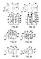
- FIG. 5shows one pattern of individual optical elements 5 on a film 2 . These optical elements may take many different shapes.
- FIG. 5 ashows one of the optical elements 5 of FIG. 5 which is a non-prismatic optical element having a total of two surfaces 10 , 12 , both of which are sloping.
- One of the surfaces 10 shown in FIG. 5 ais planar or flat whereas the other surface 12 is curved.
- both surfaces 10 , 12intersect each other and also intersect the surface of the film.
- both surfaces 10 ′, 12 ′ of the individual optical elements 5 ′may be curved as schematically shown in FIG. 5 b.
- the optical elementsmay each have only one surface that is curved and sloping and intersects the film.
- FIG. 5 cshows one such optical element 5 II in the shape of a cone 13
- FIG. 5 dshows another such optical element 5 III having a semispherical or dome shape 14 .
- such optical elementsmay have more than one sloping surface intersecting the film.
- FIG. 5 eshows an optical element 5 IV having a total of three surfaces, all of which intersect the film and intersect each other. Two of the surfaces 15 and 16 are curved, whereas the third surface 17 is planar.
- FIG. 5 fshows an optical element 5 in the shape of a pyramid 18 with four triangular shaped sides 19 that intersect each other and intersect the film.
- the sides 19 of the pyramid 18may all be of the same size and shape as shown in FIG. 5 f , or the sides 19 I of the pyramid 18 I may be stretched so the sides of the optical element 5 VI have different perimeter shapes as shown in FIG. 5 g .
- the optical elementsmay have any number of planar sloping sides.
- FIG. 5 hshows an optical element 5 VII with four planar sloping sides 20
- FIG. 5 ishows an optical element 5 VIII with eight planar sloping sides 20 I .
- the individual optical elementsmay also have more than one curved and more than one planar sloping surface, all intersecting the film.
- FIG. 5 jshows an optical element 5 IX having a pair of intersecting oppositely sloping planar sides 22 and oppositely rounded or curved ends or sides 23 .
- the sloping planar sides 22 I and 22 II and curved ends or sides 23 I and 23 II of optical elements 5 X and 5 Ximay have different angled slopes as shown in FIGS. 5 k and 5 l .
- the optical elementsmay have at least one curved surface that does not intersect the film.
- One such optical element 5 XIIis shown in FIG.
- optical elements 5 XIIImay be curved along their length as shown in FIG. 5 n.
- the individual optical elementswith a combination of planar and curved surfaces redirects or redistributes a larger viewing area than is possible with a grooved film.
- the curvature of the surfaces, or the ratio of the curved area to the planar area of the individual optical elementsmay be varied to tailor the light output distribution of the film to customize the viewing area of a display device used in conjunction with the film.
- the light entrance surface 7 of the film 2may have an optical coating 25 (see FIG. 2 ) such as an antireflective coating, a reflective polarizer, a retardation coating or a polarizer.
- an optical coating 25such as an antireflective coating, a reflective polarizer, a retardation coating or a polarizer.
- a matte or diffuse texturemay be provided on the light entrance surface 7 depending on the visual appearance desired. A matte finish produces a softer image but is not as bright.
- the combination of planar and curved surfaces of the individual optical elements of the present inventionmay be configured to redirect some of the light rays impinging thereon in different directions to produce a softer image without the need for an additional diffuser or matte finish on the entrance surface of the film.
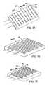
- FIGS. 6 , 7 , 13 and 15show optical elements 5 XIV , 5 XV , 5 XVI , and 5 XVII of light redirecting films 2 I , 2 II , 2 III and 2 IV staggered with respect to each other;
- FIGS. 8-10show the optical elements 5 XVIII , 5 XIX and 5 XX of light redirecting films 2 V , 2 VI and 2 VII intersecting each other;
- FIGS. 11 and 12show the optical elements intersecting 5 XXI and 5 XXII of light redirecting films 2 VIII and 2 IX interlocking each other.
- the slope angle, density, position, orientation, height or depth, shape, and/or size of the optical elements of the light redirecting filmmay be matched or tuned to the particular light output distribution of a backlight BL or other light source to account for variations in the distribution of light emitted by the backlight in order to redistribute more of the light emitted by the backlight within a desired viewing angle.
- the angle that the sloping surfaces (e.g., surfaces 10 , 12 ) of the optical elements 5 make with the surface of the light redirecting film 2may be varied as the distance from the backlight BL from a light source 26 increases to account for the way the backlight emits light rays R at different angles as the distance from the light source increases as schematically shown in FIG.
- the backlight BLitself may be designed to emit more of the light rays at lower angles to increase the amount of light emitted by the backlight and rely on the light redirecting film to redistribute more of the emitted light within a desired viewing angle.
- the individual optical elements of the light redirecting filmmay be selected to work in conjunction with the optical deformations of the backlight to produce an optimized output light ray angle distribution from the system.
- FIGS. 2 , 5 and 9show different patterns of individual optical elements all of the same height or depth
- FIGS. 7 , 8 , 10 , 13 and 14show different patterns of individual optical elements of different shapes, sizes and height or depth.
- the individual optical elements 5 XXIII of the light redirecting film 2 X of FIG. 14are also shown arranged in alternating rows along the width or length of the film.
- the individual optical elements 5 XXV and 5 XXVImay also be randomized on the film 2 XI and 2 XII as schematically shown in FIGS. 16 and 17 in such a way as to eliminate any interference with the pixel spacing of a liquid crystal display. This eliminates the need for optical diffuser layers 30 shown in FIGS. 1 and 2 to defeat moiré and similar effects.
- at least some of the individual optical elementsmay be arranged in groupings 32 , 32 I and 32 II across the film, with at least some of the optical elements in each grouping having a different size or shape characteristic that collectively produce an average size or shape characteristic for each of the groupings that varies across the film as schematically shown in FIGS.
- At least some of the optical elements in each groupingmay have a different depth or height that collectively produce an average depth or height characteristic for each grouping that varies across the film. Also, at least some of the optical elements in each grouping may have a different slope angle that collectively produce an average slope angle for each grouping that varies across the film. Further, at least one sloping surface of the individual optical elements in each grouping may have a different width or length that collectively produce an average width or length characteristic in each grouping that varies across the film.
- the individual optical elementsinclude a combination of planar and curved surfaces, for example planar and curved surfaces 10 II , 12 II , 10 III , 12 III and 10 IV , 12 IV as shown in FIGS. 7 , 13 and 15 , respectively, the curvature of the curved surfaces, or the ratio of the curved area to the planar area of the individual optical elements as well as the perimeter shapes of the curved and planar surfaces may be varied to tailor the light output distribution of the film.
- the curvature of the curved surfaces, or the ratio of the curved area to the planar area of the individual optical elementsmay be varied to redirect more or less light that is traveling in a plane that would be parallel to the grooves of a prismatic or lenticular grooved film, partially or completely replacing the need for a second layer of light redirecting film.
- at least some of the individual optical elementsmay be oriented at different angles relative to each other as schematically shown in FIGS. 13 and 16 to redistribute more of the light emitted by a light source along two different axes in a direction more normal to the surface of the film, partially or completely replacing the need for a second layer of light redirecting film.
- two layers of such light redirecting filmeach having the same or different patterns of individual optical elements thereon may be placed between a light source and viewing area with the layers rotated 90 degrees (or other angles greater than 0 degrees and less than 90 degrees) with respect to each other so that the individual optical elements on the respective film layers redistribute more of the light emitted by a light source traveling in different planar directions in a direction more normal to the surface of the respective films.
- the light redirecting film 2 IVmay have a pattern of optical elements 5 XVII that varies at different locations on the film as schematically shown in FIG. 15 to redistribute the light ray output distribution from different locations of a backlight or other light source to redistribute the light ray output distribution from the different locations toward a direction normal to the film.
- the properties and pattern of the optical elements of the light redirecting filmmay be customized to optimize the light redirecting film for different types of light sources which emit different light distributions, for example, one pattern for single bulb laptops, another pattern for double bulb flat panel displays, and so on.
- FIG. 17shows the optical elements 5 XXVI arranged in a radial pattern from the outside edges of the film 2 XII toward the center to redistribute the light ray output distribution of a backlight BL that receives light from cold cathode fluorescent lamp 26 I along all four side edges of the backlight.
- FIG. 18shows the optical elements 5 XXVII arranged in a pattern of angled groupings 32 III across the film 2 that are tailored to redistribute the light ray output distribution of a backlight BL that receives light from one cold cathode fluorescent lamp 26 I or a plurality of light emitting diodes 26 II along one input edge of the backlight.
- FIG. 19shows the optical elements 5 XXVIII arranged in a radial type pattern facing a corner of the film 2 XIV to redistribute the light ray output distribution of a backlight BL that is corner lit by a light emitting diode 26 II .
- FIG. 20shows the optical elements 5 XXIX arranged in a radial type pattern facing a midpoint on one input edge of the film 2 XV to redistribute the light ray output distribution of a backlight BL that is lighted at a midpoint of one input edge of the backlight by a single light emitting diode 26 II .
- FIG. 21shows a light redirecting film 2 XVI having optical grooves 35 extending across the film in a curved pattern facing a corner of the film to redistribute the light ray output distribution of a backlight BL that is corner lit by a light emitting diode 26 II
- FIGS. 22-24show a light redirecting film 2 XVII having a pattern of optical grooves 35 I extending across the film facing a midpoint along one edge of the film that decreases in curvature as the distance from the one edge increases to redistribute the light ray output distribution of a backlight BL that is edge lit by a light emitting diode 26 II at a midpoint of one input edge of the backlight.
- a roll 41 of the filmmay be provided having a repeating pattern of optical elements thereon as schematically shown in FIG. 15 to permit a selected area of the pattern that best suits a particular application to be die cut from the roll of film.
- the backlight BLmay be substantially flat, or curved, or may be a single layer or multi-layers, and may have different thicknesses and shapes as desired. Moreover, the backlight may be flexible or rigid, and be made of a variety of compounds. Further, the backlight may be hollow, filled with liquid, air, or be solid, and may have holes or ridges.
- the light source 26may be of any suitable type including, for example, an arc lamp, an incandescent bulb which may also be colored, filtered or painted, a lens end bulb, a line light, a halogen lamp, a light emitting diode (LED), a chip from an LED, a neon bulb, a cold cathode fluorescent lamp, a fiber optic light pipe transmitting from a remote source, a laser or laser diode, or any other suitable light source.
- the light source 26may be a multiple colored LED, or a combination of multiple colored radiation sources in order to provide a desired colored or white light output distribution.
- a plurality of colored lightssuch as LEDs of different colors (e.g., red, blue, green) or a single LED with multiple color chips may be employed to create white light or any other colored light output distribution by varying the intensities of each individual colored light.
- LEDs of different colorse.g., red, blue, green
- a single LED with multiple color chipsmay be employed to create white light or any other colored light output distribution by varying the intensities of each individual colored light.
- a pattern of optical deformitiesmay be provided on one or both sides of the backlight BL or on one or more selected areas on one or both sides of the backlight as desired.
- optical deformitiesmeans any change in the shape or geometry of a surface and/or coating or surface treatment that causes a portion of the light to be emitted from the backlight.
- These deformitiescan be produced in a variety of manners, for example, by providing a painted pattern, an etched pattern, machined pattern, a printed pattern, a hot stamp pattern, or a molded pattern or the like on selected areas of the backlight.
- An ink or print patternmay be applied for example by pad printing, silk printing, inkjet, heat transfer film process or the like.
- the deformitiesmay also be printed on a sheet or film which is used to apply the deformities to the backlight.
- This sheet or filmmay become a permanent part of the backlight for example by attaching or otherwise positioning the sheet or film against one or both sides of the backlight in order to produce a desired effect.
- the light output of the backlightcan be controlled.
- the deformitiesmay be used to control the percent of light output from a light emitting area of the backlight. For example, less and/or smaller size deformities may be placed on surface areas where less light output is wanted. Conversely, a greater percentage of and/or larger deformities may be placed on surface areas of the backlight where greater light output is desired.
- Varying the percentages and/or size of deformities in different areas of the backlightis necessary in order to provide a substantially uniform light output distribution.
- the amount of light traveling through the backlightwill ordinarily be greater in areas closer to the light source than in other areas further removed from the light source.
- a pattern of deformitiesmay be used to adjust for the light variances within the backlight, for example, by providing a denser concentration of deformities with increased distance from the light source thereby resulting in a more uniform light output distribution from the backlight.
- the deformitiesmay also be used to control the output ray angle distribution from the backlight to suit a particular application. For example, if the backlight is used to backlight a liquid crystal display, the light output will be more efficient if the deformities (or a light redirecting film is used in combination with the backlight) direct the light rays emitted by the backlight at predetermined ray angles such that they will pass through the liquid crystal display with low loss. Additionally, the pattern of optical deformities may be used to adjust for light output variances attributed to light extractions of the backlight.
- the pattern of optical deformitiesmay be printed on the backlight surface areas utilizing a wide spectrum of paints, inks, coatings, epoxies or the like, ranging from glossy to opaque or both, and may employ half-tone separation techniques to vary the deformity coverage. Moreover, the pattern of optical deformities may be multiple layers or vary in index of refraction.
- Print patterns of optical deformitiesmay vary in shapes such as dots, squares, diamonds, ellipses, stars, random shapes, and the like. Also, print patterns of sixty lines per inch or finer are desirably employed. This makes the deformities or shapes in the print patterns nearly invisible to the human eye in a particular application, thereby eliminating the detection of gradient or banding lines that are common to light extracting patterns utilizing larger elements. Additionally, the deformities may vary in shape and/or size along the length and/or width of the backlight. Also, a random placement pattern of the deformities may be utilized throughout the length and/or width of the backlight. The deformities may have shapes or a pattern with no specific angles to reduce moiré or other interference effects.
- Examples of methods to create these random patternsare printing a pattern of shapes using stochastic print pattern techniques, frequency modulated half tone patterns, or random dot half tones.
- the deformitiesmay be colored in order to effect color correction in the backlight.
- the color of the deformitiesmay also vary throughout the backlight, for example, to provide different colors for the same or different light output areas.
- optical deformitiesincluding prismatic or lenticular grooves or cross grooves, or depressions or raised surfaces of various shapes using more complex shapes in a mold pattern may be molded, etched, stamped, thermoformed, hot stamped or the like into or on one or more surface areas of the backlight.
- the prismatic or lenticular surfaces, depressions or raised surfaceswill cause a portion of the light rays contacted thereby to be emitted from the backlight.
- the angles of the prisms, depressions or other surfacesmay be varied to direct the light in different directions to produce a desired light output distribution or effect.
- the reflective or refractive surfacesmay have shapes or a pattern with no specific angles to reduce moiré or other interference effects.
- a back reflector 42may be attached or positioned against one side of the backlight BL as schematically shown in FIGS. 1 and 2 in order to improve light output efficiency of the backlight by reflecting the light emitted from that side back through the backlight for emission through the opposite side.
- a pattern of optical deformities 50may be provided on one or both sides of the backlight as schematically shown in FIGS. 1 and 2 in order to change the path of the light so that the internal critical angle is exceeded and a portion of the light is emitted from one or both sides of the backlight.
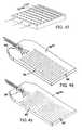
- FIGS. 25-28show optical deformities 50 I , 50 II which may either be individual projections 51 on the respective backlight surface areas 52 or individual depressions 53 in such surface areas 52 I of a backlight Bl I , BL II .
- each of these optical deformitieshas a well defined shape including a reflective or refractive surface 54 , 54 I (hereafter sometimes collectively referred to as a reflective/refractive surface) that intersects the respective backlight surface area 52 , 52 I at one edge 55 , 55 I and has a uniform slope throughout its length for more precisely controlling the emission of light by each of the deformities.
- each reflective/refractive surface 54 , 54 Iis an end wall 57 , 57 I of each deformity that intersects the respective panel surface area 52 , 52 I at a greater included angle I, I I than the included angle I II , I III between the reflective/refractive surfaces 54 , 54 I and the panel surface area 52 , 52 I (see FIGS. 27 and 28 ) to minimize the projected surface area of the end walls on the panel surface area.
- Thisallows more deformities to be placed on or in the panel surface areas than would otherwise be possible if the projected surface areas of the end walls 57 , 57 I were substantially the same as or greater than the projected surface areas of the reflective/refractive surfaces 54 , 54 I .
- FIGS. 25 and 26the peripheral edge portions 56 , 56 I of the reflective/refractive surfaces 54 , 54 I and associated end walls 57 , 57 I are curved in the transverse direction. Also in FIGS. 27 and 28 the end walls 57 , 57 I of the deformities are shown extending substantially perpendicular to the reflective/refractive surfaces 54 , 54 I of the deformities. Alternatively, such end walls may extend substantially perpendicular to the panel surface areas 52 , 52 I as schematically shown in FIGS. 29 and 30 . This virtually eliminates any projected surface area of the end walls on the panel surface areas whereby the density of the deformities on the panel surface areas may be even further increased.
- the optical deformitiesmay also be of other well defined shapes to obtain a desired light output distribution from a panel surface area.
- FIG. 31shows individual light extracting deformities 58 on a panel surface area 52 III each including a generally planar, rectangular reflective/refractive surface 59 and associated end wall 60 of a uniform slope throughout their length and width and generally planar side walls 61 .
- the deformities 58 Imay have rounded or curved side walls 62 on a panel surface area 52 IV as schematically shown in FIG. 32 .
- FIG. 33shows individual light extracting deformities 63 on a panel surface area 52 V each including a planar, sloping triangular shaped reflective/refractive surface 64 and associated planar, generally triangularly shaped side walls or end walls 65 .
- FIG. 34shows individual light extracting deformities 66 on a panel surface area 52 VI each including a planar sloping reflective/refractive surface 67 having angled peripheral edge portions 68 and associated angled end and side walls 69 and 70 .
- FIG. 35shows individual light extracting deformities 71 on a panel surface area 52 VII which are generally conically shaped
- FIG. 36shows individual light extracting deformities 72 on a panel surface area 52 VII each including a rounded reflective/refractive surface 73 and rounded end walls 74 and rounded or curved side walls 75 all blended together.
- These additional surfaceswill reflect or refract other light rays impinging thereon in different directions to spread light across the backlight/panel member BL to provide a more uniform distribution of light emitted from the panel member.
- FIGS. 37-39show deformities 76 , 77 and 78 in the form of individual projections on a panel surface area 52 IX , 52 X , 52 XI having representative shapes similar to those shown in FIGS. 31 , 32 and 35 , respectively, except that each deformity is intersected by a planar surface 79 , 79 I , 79 II in parallel spaced relation to the panel surface area.
- FIG. 37-39show deformities 76 , 77 and 78 in the form of individual projections on a panel surface area 52 IX , 52 X , 52 XI having representative shapes similar to those shown in FIGS. 31 , 32 and 35 , respectively, except that each deformity is intersected by a planar surface 79 , 79 I , 79 II in parallel spaced relation to the panel surface area.
- FIG. 37-39show deformities 76 , 77 and 78 in the form of individual projections on a panel surface area 52 IX , 52 X
- FIG. 40shows one of a multitude of deformities 80 in the form of individual depressions 81 in a panel surface area 52 XII each intersected by a planar surface 79 III in parallel spaced relation to the general planar surface of the panel surface area. Any light rays that impinge on such planar surfaces at internal angles less than the critical angle for emission of light from the panel surface area will be internally reflected by the planar surfaces, whereas any light rays impinging on such planar surfaces at internal angles greater than the critical angle will be emitted by the planar surfaces with minimal optical discontinuities, as schematically shown in FIG. 40 .
- the reflective/refractive surfacesextend at an angle away from the panel in a direction generally opposite to that in which the light rays from the light source 26 travel through the panel as schematically shown in FIGS. 27 and 29 .
- the reflective/refractive surfacesextend at an angle into the panel in the same general direction in which the light rays from the light source 26 travel through the panel member as schematically shown in FIGS. 28 and 30 .
- the slopes of the light reflective/refractive surfaces of the deformitiesmay be varied to cause the light rays impinging thereon to be either refracted out of the light emitting panel or reflected back through the panel and emitted out the opposite side of the panel which may be etched to diffuse the light emitted therefrom or covered by a light redirecting film to produce a desired effect.
- the pattern of optical deformities on the panel surface areamay be uniform or variable as desired to obtain a desired light output distribution from the panel surface areas.
- FIGS. 41 and 42show deformities 76 I and 77 I similar in shape to those shown in FIGS.
- FIGS. 43 and 44show such deformities 76 II and 77 II arranged in staggered rows that overlap each other along the length of a panel surface area 52 XV , 52 XVI .
- FIGS. 45 and 46show a random or variable pattern of different size deformities 58 II , 58 III similar in shape to those shown in FIGS. 31 and 32 , respectively, arranged in staggered rows on a panel surface area 52 XVII , 52 XVIII , whereas FIG. 47 shows deformities 77 III similar in shape to those shown in FIG.
- the deformitiesare shown in FIGS. 45 and 46 arranged in clusters 82 , 82 I across the panel surface, with at least some of the deformities in each cluster having a different size or shape characteristic that collectively produce an average size or shape characteristic for each of the clusters that varies across the panel surface.
- at least some of the deformities in each of the clustersmay have a different depth or height or different slope or orientation that collectively produce an average depth or height characteristic or average slope or orientation of the sloping surface that varies across the panel surface.
- each of the clustersmay have a different width or length that collectively produce an average width or length characteristic that varies across the panel surface. This allows one to obtain a desired size or shape characteristic beyond machinery tolerances, and also defeats moiré and interference effects.
- FIGS. 48 and 49schematically show different angular orientations of optical deformities 85 , 85 I of any desired shape along the length and width of a panel surface area 52 XX , 52 XXI of a light emitting panel assembly backlight.
- the deformitiesare arranged in straight rows 86 along the length of the panel surface area but the deformities in each of the rows are oriented to face the light source 26 so that all of the deformities are substantially in line with the light rays being emitted from the light source.
- the deformities 85 Iare also oriented to face the light source 26 similar to FIG. 48 .
- the rows 87 of deformities in FIG. 49are in substantial radial alignment with the light source 26 .
- FIGS. 50 and 51schematically show how exemplary light rays 90 , 90 I emitted from a focused light source 26 insert molded or cast within a light transition area 91 , 91 I of a light emitting panel assembly backlight BL III , BL IV in accordance with this invention are reflected during their travel through the light emitting panel member 92 , 92 I until they impinge upon individual light extracting deformities 50 III , 77 IV of well defined shapes on or in a panel surface area 52 XXII , 52 XXIII causing more of the light rays to be reflected or refracted out of one side 93 , 93 I of the panel member than the other side 94 , 94 I .
- FIG. 50 and 51schematically show how exemplary light rays 90 , 90 I emitted from a focused light source 26 insert molded or cast within a light transition area 91 , 91 I of a light emitting panel assembly backlight BL III , BL IV in accordance
- the exemplary light rays 90are shown being reflected by the reflective/refractive surfaces 54 III of the deformities 50 III in the same general direction out through the same side 93 of the panel member, whereas in FIG. 51 the light rays 90 I are shown being scattered in different directions within the panel member 92 I by the rounded side walls 62 I of the deformities 77 IV before the light rays are reflected/refracted out of the same side 93 I of the panel member.
- Such a pattern of individual light extracting deformities of well defined shapes in accordance with the present inventioncan cause 60 to 70% or more of the light received through the input edge 95 I of the panel member to be emitted from the same side of the panel member.
- the light redirecting films of the present inventionredistribute more of the light emitted by a backlight or other light source toward a direction more normal to the plane of the films.
- the light redirecting films and backlights of the present inventionmay be tailored or tuned to each other to provide a system in which the individual optical elements of the light redirecting films work in conjunction with the optical deformities of the backlights to produce an optimized output light ray angle distribution from the system.
Landscapes
- Physics & Mathematics (AREA)
- General Physics & Mathematics (AREA)
- Optics & Photonics (AREA)
- Health & Medical Sciences (AREA)
- Engineering & Computer Science (AREA)
- Anesthesiology (AREA)
- General Engineering & Computer Science (AREA)
- Biomedical Technology (AREA)
- Animal Behavior & Ethology (AREA)
- General Health & Medical Sciences (AREA)
- Veterinary Medicine (AREA)
- Life Sciences & Earth Sciences (AREA)
- Public Health (AREA)
- Pain & Pain Management (AREA)
- Manufacturing & Machinery (AREA)
- Acoustics & Sound (AREA)
- Psychology (AREA)
- Heart & Thoracic Surgery (AREA)
- Hematology (AREA)
- Pathology (AREA)
- Radiology & Medical Imaging (AREA)
- Nuclear Medicine, Radiotherapy & Molecular Imaging (AREA)
- Optical Elements Other Than Lenses (AREA)
- Planar Illumination Modules (AREA)
- Light Guides In General And Applications Therefor (AREA)
- Liquid Crystal (AREA)
Abstract
Description
Claims (22)
Priority Applications (2)
| Application Number | Priority Date | Filing Date | Title |
|---|---|---|---|
| US12/364,554US8092068B2 (en) | 1999-02-23 | 2009-02-03 | Light redirecting films and film systems |
| US13/313,190US8322905B2 (en) | 1999-02-23 | 2011-12-07 | Edgelit panel with curvilinear light extracting deformities |
Applications Claiming Priority (6)
| Application Number | Priority Date | Filing Date | Title |
|---|---|---|---|
| US09/256,275US6712481B2 (en) | 1995-06-27 | 1999-02-23 | Light emitting panel assemblies |
| US09/909,318US6752505B2 (en) | 1999-02-23 | 2001-07-19 | Light redirecting films and film systems |
| US10/729,113US7090389B2 (en) | 1999-02-23 | 2003-12-05 | Method of selecting a light redirecting film |
| US11/484,063US7364342B2 (en) | 1999-02-23 | 2006-07-11 | Light redirecting films pattern of variable optical elements |
| US12/054,680US7914196B2 (en) | 1999-02-23 | 2008-03-25 | Light redirecting film systems having pattern of variable optical elements |
| US12/364,554US8092068B2 (en) | 1999-02-23 | 2009-02-03 | Light redirecting films and film systems |
Related Parent Applications (1)
| Application Number | Title | Priority Date | Filing Date |
|---|---|---|---|
| US12/054,680ContinuationUS7914196B2 (en) | 1999-02-23 | 2008-03-25 | Light redirecting film systems having pattern of variable optical elements |
Related Child Applications (1)
| Application Number | Title | Priority Date | Filing Date |
|---|---|---|---|
| US13/313,190ContinuationUS8322905B2 (en) | 1999-02-23 | 2011-12-07 | Edgelit panel with curvilinear light extracting deformities |
Publications (2)
| Publication Number | Publication Date |
|---|---|
| US20090135626A1 US20090135626A1 (en) | 2009-05-28 |
| US8092068B2true US8092068B2 (en) | 2012-01-10 |
Family
ID=25427020
Family Applications (11)
| Application Number | Title | Priority Date | Filing Date |
|---|---|---|---|
| US09/909,318Expired - Fee RelatedUS6752505B2 (en) | 1999-02-23 | 2001-07-19 | Light redirecting films and film systems |
| US10/729,113Expired - LifetimeUS7090389B2 (en) | 1999-02-23 | 2003-12-05 | Method of selecting a light redirecting film |
| US11/484,063Expired - Fee RelatedUS7364342B2 (en) | 1999-02-23 | 2006-07-11 | Light redirecting films pattern of variable optical elements |
| US12/054,680Expired - Fee RelatedUS7914196B2 (en) | 1999-02-23 | 2008-03-25 | Light redirecting film systems having pattern of variable optical elements |
| US12/250,922AbandonedUS20090034293A1 (en) | 1999-02-23 | 2008-10-14 | Light redirecting films and film systems |
| US12/364,637Expired - Fee RelatedUS7810982B2 (en) | 1999-02-23 | 2009-02-03 | Edge-lit optical system having optical elements on two surfaces |
| US12/364,554Expired - Fee RelatedUS8092068B2 (en) | 1999-02-23 | 2009-02-03 | Light redirecting films and film systems |
| US12/946,077AbandonedUS20110058390A1 (en) | 1999-02-23 | 2010-11-15 | Light redirecting films and film systems |
| US13/030,881AbandonedUS20110134362A1 (en) | 1999-02-23 | 2011-02-18 | Light redirecting films and film systems |
| US13/313,190Expired - Fee RelatedUS8322905B2 (en) | 1999-02-23 | 2011-12-07 | Edgelit panel with curvilinear light extracting deformities |
| US13/893,886Expired - Fee RelatedUS8845176B2 (en) | 1999-02-23 | 2013-05-14 | Light redirecting films with non-prismatic optical elements |
Family Applications Before (6)
| Application Number | Title | Priority Date | Filing Date |
|---|---|---|---|
| US09/909,318Expired - Fee RelatedUS6752505B2 (en) | 1999-02-23 | 2001-07-19 | Light redirecting films and film systems |
| US10/729,113Expired - LifetimeUS7090389B2 (en) | 1999-02-23 | 2003-12-05 | Method of selecting a light redirecting film |
| US11/484,063Expired - Fee RelatedUS7364342B2 (en) | 1999-02-23 | 2006-07-11 | Light redirecting films pattern of variable optical elements |
| US12/054,680Expired - Fee RelatedUS7914196B2 (en) | 1999-02-23 | 2008-03-25 | Light redirecting film systems having pattern of variable optical elements |
| US12/250,922AbandonedUS20090034293A1 (en) | 1999-02-23 | 2008-10-14 | Light redirecting films and film systems |
| US12/364,637Expired - Fee RelatedUS7810982B2 (en) | 1999-02-23 | 2009-02-03 | Edge-lit optical system having optical elements on two surfaces |
Family Applications After (4)
| Application Number | Title | Priority Date | Filing Date |
|---|---|---|---|
| US12/946,077AbandonedUS20110058390A1 (en) | 1999-02-23 | 2010-11-15 | Light redirecting films and film systems |
| US13/030,881AbandonedUS20110134362A1 (en) | 1999-02-23 | 2011-02-18 | Light redirecting films and film systems |
| US13/313,190Expired - Fee RelatedUS8322905B2 (en) | 1999-02-23 | 2011-12-07 | Edgelit panel with curvilinear light extracting deformities |
| US13/893,886Expired - Fee RelatedUS8845176B2 (en) | 1999-02-23 | 2013-05-14 | Light redirecting films with non-prismatic optical elements |
Country Status (7)
| Country | Link |
|---|---|
| US (11) | US6752505B2 (en) |
| EP (2) | EP2523025A3 (en) |
| JP (1) | JP4349902B2 (en) |
| KR (3) | KR100918141B1 (en) |
| CN (2) | CN100432717C (en) |
| TW (3) | TWI243920B (en) |
| WO (1) | WO2003008860A1 (en) |
Cited By (32)
| Publication number | Priority date | Publication date | Assignee | Title |
|---|---|---|---|---|
| US20100253696A1 (en)* | 2009-04-01 | 2010-10-07 | Choi Jintaek | Liquid crystal display and driving method of thereof |
| US20110128256A1 (en)* | 2009-11-27 | 2011-06-02 | Coretronic Corporation | Light guide apparatus and optical touch display apparatus |
| US20120113158A1 (en)* | 2010-09-14 | 2012-05-10 | Dai Nippon Printing Co., Ltd. | Surface light source device, liquid crystal display device and optical member |
| US20130208451A1 (en)* | 2010-11-10 | 2013-08-15 | Lg Chem, Ltd. | Optical member and method for manufacturing same, backlight unit using the optical member, and method for manufacturing the backlight unit |
| US20130286679A1 (en)* | 2012-04-30 | 2013-10-31 | Coretronic Corporation | Light guide plate and backlight module using the same |
| US20140355302A1 (en)* | 2013-03-15 | 2014-12-04 | Cree, Inc. | Outdoor and/or Enclosed Structure LED Luminaire for General Illumination Applications, Such as Parking Lots and Structures |
| US9291320B2 (en) | 2013-01-30 | 2016-03-22 | Cree, Inc. | Consolidated troffer |
| US9366799B2 (en) | 2013-03-15 | 2016-06-14 | Cree, Inc. | Optical waveguide bodies and luminaires utilizing same |
| US9366396B2 (en) | 2013-01-30 | 2016-06-14 | Cree, Inc. | Optical waveguide and lamp including same |
| US9389367B2 (en) | 2013-01-30 | 2016-07-12 | Cree, Inc. | Optical waveguide and luminaire incorporating same |
| US9442243B2 (en) | 2013-01-30 | 2016-09-13 | Cree, Inc. | Waveguide bodies including redirection features and methods of producing same |
| US9625638B2 (en) | 2013-03-15 | 2017-04-18 | Cree, Inc. | Optical waveguide body |
| US9651740B2 (en) | 2014-01-09 | 2017-05-16 | Cree, Inc. | Extraction film for optical waveguide and method of producing same |
| US9690029B2 (en) | 2013-01-30 | 2017-06-27 | Cree, Inc. | Optical waveguides and luminaires incorporating same |
| US9798072B2 (en) | 2013-03-15 | 2017-10-24 | Cree, Inc. | Optical element and method of forming an optical element |
| US9801474B2 (en) | 2014-10-01 | 2017-10-31 | True Manufacturing Co., Inc. | Edge-lit door for refrigerator unit |
| US9869432B2 (en) | 2013-01-30 | 2018-01-16 | Cree, Inc. | Luminaires using waveguide bodies and optical elements |
| US9920901B2 (en) | 2013-03-15 | 2018-03-20 | Cree, Inc. | LED lensing arrangement |
| US10012356B1 (en) | 2017-11-22 | 2018-07-03 | LightLouver LLC | Light-redirecting optical daylighting system |
| US10185064B2 (en) | 2016-10-26 | 2019-01-22 | Microsoft Technology Licensing, Llc | Curved edge display with controlled luminance |
| US10209429B2 (en) | 2013-03-15 | 2019-02-19 | Cree, Inc. | Luminaire with selectable luminous intensity pattern |
| US10223952B2 (en) | 2016-10-26 | 2019-03-05 | Microsoft Technology Licensing, Llc | Curved edge display with controlled distortion |
| US10416377B2 (en) | 2016-05-06 | 2019-09-17 | Cree, Inc. | Luminaire with controllable light emission |
| US20190302461A1 (en)* | 2018-03-29 | 2019-10-03 | Sharp Kabushiki Kaisha | Display device and head-mounted display |
| US10436970B2 (en) | 2013-03-15 | 2019-10-08 | Ideal Industries Lighting Llc | Shaped optical waveguide bodies |
| US10502899B2 (en)* | 2013-03-15 | 2019-12-10 | Ideal Industries Lighting Llc | Outdoor and/or enclosed structure LED luminaire |
| US10598851B2 (en) | 2013-08-27 | 2020-03-24 | Nano-Lit Technologies Limited | Light diffuser |
| US10810914B2 (en) | 2017-08-09 | 2020-10-20 | True Manufacturing Co., Inc. | Illuminating display window and merchandiser display unit comprising same |
| US10900657B2 (en) | 2017-08-01 | 2021-01-26 | Technical Consumer Products, Inc. | Edge-lit light fixture having capabilities for a secondary service |
| US11112083B2 (en) | 2013-03-15 | 2021-09-07 | Ideal Industries Lighting Llc | Optic member for an LED light fixture |
| US11719882B2 (en) | 2016-05-06 | 2023-08-08 | Ideal Industries Lighting Llc | Waveguide-based light sources with dynamic beam shaping |
| US20240184032A1 (en)* | 2022-12-05 | 2024-06-06 | Lg Display Co., Ltd. | Backlight unit and display device including the same |
Families Citing this family (439)
| Publication number | Priority date | Publication date | Assignee | Title |
|---|---|---|---|---|
| US7108414B2 (en) | 1995-06-27 | 2006-09-19 | Solid State Opto Limited | Light emitting panel assemblies |
| US7364341B2 (en) | 1999-02-23 | 2008-04-29 | Solid State Opto Limited | Light redirecting films including non-interlockable optical elements |
| US6827456B2 (en)* | 1999-02-23 | 2004-12-07 | Solid State Opto Limited | Transreflectors, transreflector systems and displays and methods of making transreflectors |
| US20050024849A1 (en)* | 1999-02-23 | 2005-02-03 | Parker Jeffery R. | Methods of cutting or forming cavities in a substrate for use in making optical films, components or wave guides |
| US6752505B2 (en)* | 1999-02-23 | 2004-06-22 | Solid State Opto Limited | Light redirecting films and film systems |
| KR100965201B1 (en)* | 2001-06-12 | 2010-06-24 | 웰스테트 테라퓨틱스 코포레이션 | Compounds for the treatment of metabolic diseases |
| KR100799156B1 (en)* | 2001-07-13 | 2008-01-29 | 삼성전자주식회사 | Light guide plate, manufacturing method thereof, liquid crystal display device using the same |
| TWI258023B (en)* | 2001-11-07 | 2006-07-11 | Ibm | A prism sheet, a back-light unit using said prism sheet, and a transmission type liquid crystal display device |
| KR20050044695A (en)* | 2001-12-05 | 2005-05-12 | 솔리드 스테이트 옵토 리미티드 | Transreflectors, transreflector systems and displays and methods of making transreflectors |
| DE10201029A1 (en)* | 2002-01-11 | 2003-07-24 | Siemens Ag | display device |
| GB0202169D0 (en)* | 2002-01-30 | 2002-03-20 | Innavisions Ltd | Improvements in or relating to optical data recognition |
| WO2003091794A1 (en)* | 2002-04-24 | 2003-11-06 | Nitto Denko Corporation | Light converging system and transmission liquid crystal display |
| JP2004296215A (en)* | 2003-03-26 | 2004-10-21 | Toyota Industries Corp | Transparent substrate for planar light source, method for manufacturing transparent substrate, planar light source, and liquid crystal display device |
| JP4019886B2 (en)* | 2002-09-30 | 2007-12-12 | オムロン株式会社 | Optical film, surface light source device and liquid crystal display device |
| US7671859B2 (en)* | 2002-11-06 | 2010-03-02 | Continental Automotive Systems Us, Inc. | Thin instrument cluster with anti-reflective coating |
| EP1420462A1 (en)* | 2002-11-13 | 2004-05-19 | Heptagon Oy | Light emitting device |
| JP4436105B2 (en)* | 2002-11-29 | 2010-03-24 | 富士通株式会社 | Reflector, illumination device, light guide plate, and display device |
| US7125131B2 (en)* | 2002-12-06 | 2006-10-24 | General Electric Company | Brightness enhancement film with improved view angle |
| TWI275842B (en)* | 2002-12-20 | 2007-03-11 | Hon Hai Prec Ind Co Ltd | Light guide plate and method of making the same |
| US7417782B2 (en) | 2005-02-23 | 2008-08-26 | Pixtronix, Incorporated | Methods and apparatus for spatial light modulation |
| KR20050106082A (en)* | 2003-03-06 | 2005-11-08 | 코닌클리즈케 필립스 일렉트로닉스 엔.브이. | Collimated scanning backlight device |
| KR100584554B1 (en)* | 2003-03-25 | 2006-05-30 | 삼성전자주식회사 | Projection type image display device |
| US20050052871A1 (en)* | 2003-07-11 | 2005-03-10 | Hon Hai Precision Industry Co., Ltd. | Light-emitting diode and backlight system using the same |
| US20050130759A1 (en)* | 2003-12-12 | 2005-06-16 | Hayden Mark X. | Sports shaft with variable contour |
| KR100971392B1 (en)* | 2003-12-24 | 2010-07-21 | 엘지디스플레이 주식회사 | LCD Display |
| KR100955173B1 (en)* | 2004-03-03 | 2010-04-29 | 키모토 컴파니 리미티드 | Light control film and backlight device using the same |
| US7255462B2 (en)* | 2004-03-04 | 2007-08-14 | K-Bridge Electronics Co., Ltd. | Dimmer device for backlight module |
| TWM255146U (en)* | 2004-04-22 | 2005-01-11 | Shih-Chieh Tang | Brightness enhancement film having curved prism units |
| US7286280B2 (en)* | 2004-05-07 | 2007-10-23 | The University Of British Columbia | Brightness enhancement film for backlit image displays |
| US7160017B2 (en) | 2004-06-03 | 2007-01-09 | Eastman Kodak Company | Brightness enhancement film using a linear arrangement of light concentrators |
| US20050269742A1 (en)* | 2004-06-03 | 2005-12-08 | Wright Thomas S | Method for making tools for micro replication |
| CN103646848B (en) | 2004-06-04 | 2018-06-05 | 伊利诺伊大学评议会 | The method of assembling printable semiconductor elements and manufacture electronic device |
| US20050275132A1 (en)* | 2004-06-15 | 2005-12-15 | Eastman Kodak Company | Belt over compliant roller used with molding roller |
| US20050276949A1 (en)* | 2004-06-15 | 2005-12-15 | Eastman Kodak Company | Optical film and method of manufacture |
| US7236303B2 (en) | 2004-06-15 | 2007-06-26 | Eastman Kodak Company | Thermoplastic optical feature with high apex sharpness |
| KR20060015174A (en)* | 2004-08-13 | 2006-02-16 | 삼성전자주식회사 | Prism sheet and liquid crystal display device having same |
| KR101085444B1 (en)* | 2004-06-25 | 2011-11-21 | 삼성전자주식회사 | Optical materials, backlight assembly having same, and display device having same |
| TWI300494B (en)* | 2004-07-23 | 2008-09-01 | Hon Hai Prec Ind Co Ltd | Light guiding plate and backlight module using the same |
| KR20060018146A (en)* | 2004-08-23 | 2006-02-28 | 엘지전자 주식회사 | Prism sheet of LCD and backlight unit |
| US7212345B2 (en)* | 2004-09-13 | 2007-05-01 | Eastman Kodak Company | Randomized patterns of individual optical elements |
| JP2006086075A (en)* | 2004-09-17 | 2006-03-30 | Alps Electric Co Ltd | Surface-emitting device, back surface-lighting system and liquid crystal display |
| US7466484B2 (en)* | 2004-09-23 | 2008-12-16 | Rohm And Haas Denmark Finance A/S | Wire grid polarizers and optical elements containing them |
| TWI249257B (en)* | 2004-09-24 | 2006-02-11 | Epistar Corp | Illumination apparatus |
| US7775700B2 (en)* | 2004-10-01 | 2010-08-17 | Rohm And Haas Electronics Materials Llc | Turning film using array of roof prism structures |
| JP2006113271A (en)* | 2004-10-14 | 2006-04-27 | Toppan Printing Co Ltd | Backlight unit for liquid crystal display |
| US20060083004A1 (en)* | 2004-10-15 | 2006-04-20 | Eastman Kodak Company | Flat-panel area illumination system |
| JP2006148036A (en)* | 2004-10-19 | 2006-06-08 | Omron Corp | Light emitting light source and light emitting light source array |
| KR101082904B1 (en)* | 2004-10-25 | 2011-11-11 | 삼성전자주식회사 | Light guide panel, and back light assembly and display device having the same |
| WO2006052755A2 (en)* | 2004-11-04 | 2006-05-18 | Solid State Opto Limited | Long curved wedges in an optical film |
| US20060103777A1 (en)* | 2004-11-15 | 2006-05-18 | 3M Innovative Properties Company | Optical film having a structured surface with rectangular based prisms |
| EP1666936A1 (en) | 2004-12-02 | 2006-06-07 | Asulab S.A. | Dual illumination function optical device and figurative image formation |
| EP1666933A1 (en) | 2004-12-02 | 2006-06-07 | Asulab S.A. | Dual illumination function optical device and figurative image formation |
| US7320538B2 (en)* | 2004-12-30 | 2008-01-22 | 3M Innovative Properties Company | Optical film having a structured surface with concave pyramid-shaped structures |
| US7220026B2 (en)* | 2004-12-30 | 2007-05-22 | 3M Innovative Properties Company | Optical film having a structured surface with offset prismatic structures |
| US7416309B2 (en)* | 2004-12-30 | 2008-08-26 | 3M Innovative Properties Company | Optical film having a surface with rounded structures |
| CN1808234A (en)* | 2005-01-20 | 2006-07-26 | 鸿富锦精密工业(深圳)有限公司 | Light guide plate |
| GB0502453D0 (en) | 2005-02-05 | 2005-03-16 | Cambridge Flat Projection | Flat panel lens |
| US7304785B2 (en) | 2005-02-23 | 2007-12-04 | Pixtronix, Inc. | Display methods and apparatus |
| US8482496B2 (en) | 2006-01-06 | 2013-07-09 | Pixtronix, Inc. | Circuits for controlling MEMS display apparatus on a transparent substrate |
| US7271945B2 (en) | 2005-02-23 | 2007-09-18 | Pixtronix, Inc. | Methods and apparatus for actuating displays |
| US20070205969A1 (en) | 2005-02-23 | 2007-09-06 | Pixtronix, Incorporated | Direct-view MEMS display devices and methods for generating images thereon |
| US7755582B2 (en) | 2005-02-23 | 2010-07-13 | Pixtronix, Incorporated | Display methods and apparatus |
| US9158106B2 (en) | 2005-02-23 | 2015-10-13 | Pixtronix, Inc. | Display methods and apparatus |
| US9229222B2 (en) | 2005-02-23 | 2016-01-05 | Pixtronix, Inc. | Alignment methods in fluid-filled MEMS displays |
| US7304786B2 (en) | 2005-02-23 | 2007-12-04 | Pixtronix, Inc. | Methods and apparatus for bi-stable actuation of displays |
| US7502159B2 (en) | 2005-02-23 | 2009-03-10 | Pixtronix, Inc. | Methods and apparatus for actuating displays |
| US9261694B2 (en) | 2005-02-23 | 2016-02-16 | Pixtronix, Inc. | Display apparatus and methods for manufacture thereof |
| US7746529B2 (en) | 2005-02-23 | 2010-06-29 | Pixtronix, Inc. | MEMS display apparatus |
| US7675665B2 (en) | 2005-02-23 | 2010-03-09 | Pixtronix, Incorporated | Methods and apparatus for actuating displays |
| US8519945B2 (en) | 2006-01-06 | 2013-08-27 | Pixtronix, Inc. | Circuits for controlling display apparatus |
| US7405852B2 (en) | 2005-02-23 | 2008-07-29 | Pixtronix, Inc. | Display apparatus and methods for manufacture thereof |
| US7742016B2 (en) | 2005-02-23 | 2010-06-22 | Pixtronix, Incorporated | Display methods and apparatus |
| US7616368B2 (en) | 2005-02-23 | 2009-11-10 | Pixtronix, Inc. | Light concentrating reflective display methods and apparatus |
| US8159428B2 (en) | 2005-02-23 | 2012-04-17 | Pixtronix, Inc. | Display methods and apparatus |
| US9082353B2 (en) | 2010-01-05 | 2015-07-14 | Pixtronix, Inc. | Circuits for controlling display apparatus |
| US9087486B2 (en) | 2005-02-23 | 2015-07-21 | Pixtronix, Inc. | Circuits for controlling display apparatus |
| US8310442B2 (en) | 2005-02-23 | 2012-11-13 | Pixtronix, Inc. | Circuits for controlling display apparatus |
| US7999994B2 (en) | 2005-02-23 | 2011-08-16 | Pixtronix, Inc. | Display apparatus and methods for manufacture thereof |
| US20100061093A1 (en)* | 2005-03-12 | 2010-03-11 | Janssen Jeffrey R | Illumination devices and methods for making the same |
| TWM276217U (en)* | 2005-04-22 | 2005-09-21 | Innolux Display Corp | Backlight module and liquid crystal display |
| TW200638075A (en)* | 2005-04-22 | 2006-11-01 | Hon Hai Prec Ind Co Ltd | Light guide plate and backlight module using the same |
| US20060250707A1 (en)* | 2005-05-05 | 2006-11-09 | 3M Innovative Properties Company | Optical film having a surface with rounded pyramidal structures |
| US8596824B2 (en)* | 2005-05-24 | 2013-12-03 | Syncrolite, L.P. | Method and apparatus for a scrollable modifier for a light fixture |
| US20060268558A1 (en)* | 2005-05-24 | 2006-11-30 | Synchrolite, L.P. | Method and apparatus for controlling diffusion and color of a light beam |
| US8721123B2 (en) | 2008-01-18 | 2014-05-13 | Syncrolite, Llc | Pattern generator for a light fixture |
| KR100728368B1 (en)* | 2005-05-25 | 2007-06-14 | 엘지전자 주식회사 | Backlight unit of liquid crystal display including conical luminance enhancing film and manufacturing method of conical luminance enhancing film |
| KR100682875B1 (en)* | 2005-06-08 | 2007-02-15 | 삼성전기주식회사 | Light guide plate with multi-cycle pattern and lighting device for display device using same |
| US8641259B2 (en)* | 2006-06-09 | 2014-02-04 | Ubright Optronics Corporation | Luminance enhancement optical substrates with anti-interference-fringe structures |
| TWI351550B (en)* | 2005-06-09 | 2011-11-01 | Ubright Optronics Corp | Optical substrate |
| US9366875B2 (en)* | 2005-06-09 | 2016-06-14 | Ubright Optronics Corporation | Light directing film |
| JP4457979B2 (en) | 2005-06-13 | 2010-04-28 | セイコーエプソン株式会社 | Backlight unit manufacturing method, backlight unit, electro-optical device, and electronic apparatus |
| DE102005027737B4 (en)* | 2005-06-16 | 2013-03-28 | Saint-Gobain Glass Deutschland Gmbh | Use of a transparent disc with a three-dimensional surface structure as a cover plate for components for the use of sunlight |
| TWI274896B (en)* | 2005-06-30 | 2007-03-01 | Efun Technology Co Ltd | Brightness enhancement film having reinforcing layer |
| JP4329736B2 (en)* | 2005-07-04 | 2009-09-09 | セイコーエプソン株式会社 | Optical substrate, planar illumination device, electro-optical device |
| US20070014020A1 (en)* | 2005-07-13 | 2007-01-18 | Eastman Kodak Company | Low birefringent light redirecting film |
| US20070024994A1 (en)* | 2005-07-29 | 2007-02-01 | 3M Innovative Properties Company | Structured optical film with interspersed pyramidal structures |
| KR101298786B1 (en)* | 2005-08-27 | 2013-08-22 | 쓰리엠 이노베이티브 프로퍼티즈 컴파니 | Illumination assembly and system |
| US7815355B2 (en)* | 2005-08-27 | 2010-10-19 | 3M Innovative Properties Company | Direct-lit backlight having light recycling cavity with concave transflector |
| US20070047228A1 (en)* | 2005-08-27 | 2007-03-01 | 3M Innovative Properties Company | Methods of forming direct-lit backlights having light recycling cavity with concave transflector |
| US7537374B2 (en)* | 2005-08-27 | 2009-05-26 | 3M Innovative Properties Company | Edge-lit backlight having light recycling cavity with concave transflector |
| TWI391711B (en)* | 2005-09-13 | 2013-04-01 | Efun Technology Co Ltd | Brightness enhancement film having a light-guiding layer |
| US20070058391A1 (en)* | 2005-09-14 | 2007-03-15 | Wilson Randall H | Light extraction layer |
| US7663712B2 (en)* | 2005-10-10 | 2010-02-16 | Skc Haas Display Films Co., Ltd. | Backlight unit with linearly reduced divergence having the width of an output aperture vary over the length of a light divergence reduction structure |
| US20070103910A1 (en)* | 2005-11-08 | 2007-05-10 | Eastman Kodak Company | Light redirecting films having multiple layers and an adhesion layer |
| US7459899B2 (en)* | 2005-11-21 | 2008-12-02 | Thermo Fisher Scientific Inc. | Inductively-coupled RF power source |
| WO2007067692A1 (en)* | 2005-12-06 | 2007-06-14 | Ubright Optronics Corporation | Luminance enhancement optical substrates with anti-chatter structures |
| TW200725076A (en)* | 2005-12-29 | 2007-07-01 | Speed Tech Corp | Method of adjusting diffusing and condensing light ability of optical element |
| US20070159845A1 (en)* | 2006-01-12 | 2007-07-12 | Omron Corporation | Surface light source device and apparatus using the same |
| US7674028B2 (en)* | 2006-01-13 | 2010-03-09 | Avery Dennison Corporation | Light enhancing structures with multiple arrays of elongate features of varying characteristics |
| US20070086207A1 (en)* | 2006-01-13 | 2007-04-19 | Optical Research Associates | Display systems including light enhancing structures with arrays of elongate features |
| US7866871B2 (en)* | 2006-01-13 | 2011-01-11 | Avery Dennison Corporation | Light enhancing structures with a plurality of arrays of elongate features |
| CN101000387A (en)* | 2006-01-14 | 2007-07-18 | 鸿富锦精密工业(深圳)有限公司 | Prism and backlight module using the prism |
| CN101025516A (en)* | 2006-02-23 | 2007-08-29 | 鸿富锦精密工业(深圳)有限公司 | Backlight module |
| US8526096B2 (en) | 2006-02-23 | 2013-09-03 | Pixtronix, Inc. | Mechanical light modulators with stressed beams |
| CN100468089C (en)* | 2006-03-03 | 2009-03-11 | 鸿富锦精密工业(深圳)有限公司 | Prism sheet and backlight module using the prism sheet |
| KR101234098B1 (en)* | 2006-03-21 | 2013-02-19 | 삼성디스플레이 주식회사 | Optical sheet, backlight assembly and display device having the same |
| US20070223252A1 (en)* | 2006-03-24 | 2007-09-27 | Junwon Lee | Illumination apparatus and film |
| CN100498389C (en)* | 2006-03-25 | 2009-06-10 | 鸿富锦精密工业(深圳)有限公司 | Light conducting plate and back light module |
| US20080081132A1 (en)* | 2006-03-30 | 2008-04-03 | Bourdelais Robert P | Light redirecting film having surface nano-nodules |
| JP2007273091A (en)* | 2006-03-30 | 2007-10-18 | Fujitsu Ltd | Prism light guide plate, lighting device and electronic device |
| JP2007280635A (en)* | 2006-04-03 | 2007-10-25 | Hitachi Displays Ltd | Surface light source device and liquid crystal display device using the same |
| FR2900220B1 (en)* | 2006-04-24 | 2008-07-18 | Valeo Vision Sa | LIGHTING OR SIGNALING DEVICE WITH DEPTH EFFECT. |
| KR100751519B1 (en)* | 2006-05-08 | 2007-08-23 | 미래나노텍(주) | Back light assembly of the liquid crystal display device provided with the optical sheet and the optical sheet |
| US7677146B2 (en)* | 2006-05-10 | 2010-03-16 | 3M Innovative Properties Company | Cutting tool using one or more machined tool tips in a continuous or interrupted cut fast tool servo |
| US7842376B2 (en)* | 2006-05-24 | 2010-11-30 | Zhijian Lu | Diffusers and methods of manufacture |
| US20070279935A1 (en)* | 2006-05-31 | 2007-12-06 | 3M Innovative Properties Company | Flexible light guide |
| US7876489B2 (en) | 2006-06-05 | 2011-01-25 | Pixtronix, Inc. | Display apparatus with optical cavities |
| TW200745490A (en)* | 2006-06-07 | 2007-12-16 | Jeng Shiang Prec Ind Co Ltd | Light guide plate |
| RU2006119965A (en)* | 2006-06-07 | 2007-12-27 | Самсунг Электроникс Ко., Лтд. (KR) | OPTICAL FILM |
| US7670726B2 (en)* | 2006-07-20 | 2010-03-02 | Zhijian Lu | Optical diffusers, photomasks and their methods of fabrication |
| US20080024870A1 (en)* | 2006-07-27 | 2008-01-31 | Bourdelais Robert P | Light-redirecting film containing optical modification layer |
| US20080032096A1 (en)* | 2006-08-07 | 2008-02-07 | Eastman Kodak Company | Microstructured film containing polysulfone polymer |
| US7498534B2 (en)* | 2006-08-30 | 2009-03-03 | 3M Innovative Properties Company | Keypad light guide |
| US7643218B2 (en)* | 2006-08-31 | 2010-01-05 | Skc Haas Display Films Co., Ltd. | Light redirecting film having varying optical elements |
| US8525402B2 (en) | 2006-09-11 | 2013-09-03 | 3M Innovative Properties Company | Illumination devices and methods for making the same |
| US8581393B2 (en) | 2006-09-21 | 2013-11-12 | 3M Innovative Properties Company | Thermally conductive LED assembly |
| US7481563B2 (en)* | 2006-09-21 | 2009-01-27 | 3M Innovative Properties Company | LED backlight |
| EP2080045A1 (en) | 2006-10-20 | 2009-07-22 | Pixtronix Inc. | Light guides and backlight systems incorporating light redirectors at varying densities |
| US20080101759A1 (en)* | 2006-10-26 | 2008-05-01 | K Laser Technology, Inc. | Prism matrix with random phase structures |
| WO2008127401A2 (en) | 2006-11-03 | 2008-10-23 | Trustees Of Tufts College | Biopolymer optical waveguide and method of manufacturing the same |
| EP2650112B1 (en) | 2006-11-03 | 2016-08-24 | Trustees Of Tufts College | Nanopatterned biopolymer optical device and method of manufacturing the same |
| US20100046902A1 (en) | 2006-11-03 | 2010-02-25 | Trustees Of Tufts College | Biopolymer photonic crystals and method of manufacturing the same |
| US20080106899A1 (en)* | 2006-11-03 | 2008-05-08 | Entire Technology Co., Ltd. | Direct backlight module |
| JP2010509593A (en)* | 2006-11-03 | 2010-03-25 | トラスティーズ オブ タフツ カレッジ | Biopolymer sensor and manufacturing method thereof |
| CN101529280B (en)* | 2006-11-09 | 2011-08-03 | 夏普株式会社 | Prism sheet and liquid crystal display device |
| CN101191870A (en)* | 2006-11-24 | 2008-06-04 | 鸿富锦精密工业(深圳)有限公司 | Optical plate and its preparation method |
| US7661849B2 (en)* | 2006-11-27 | 2010-02-16 | Ping Sun Patrick Lo | Illuminated apparatus |
| CN101191945B (en)* | 2006-11-29 | 2010-11-10 | 清华大学 | Backlight module group |
| CN101191849A (en)* | 2006-12-01 | 2008-06-04 | 鸿富锦精密工业(深圳)有限公司 | optical board |
| CN101196584A (en)* | 2006-12-08 | 2008-06-11 | 鸿富锦精密工业(深圳)有限公司 | optical board |
| US7628100B2 (en)* | 2007-01-05 | 2009-12-08 | 3M Innovative Properties Company | Cutting tool using one or more machined tool tips with diffractive features in a continuous or interrupted cut fast tool servo |
| KR100903028B1 (en)* | 2007-01-15 | 2009-06-18 | 제일모직주식회사 | LGP for backlight unit of liquid crystal display including wedge back prism |
| US7852546B2 (en) | 2007-10-19 | 2010-12-14 | Pixtronix, Inc. | Spacers for maintaining display apparatus alignment |
| US9176318B2 (en) | 2007-05-18 | 2015-11-03 | Pixtronix, Inc. | Methods for manufacturing fluid-filled MEMS displays |
| US20080188277A1 (en) | 2007-02-01 | 2008-08-07 | Ritter Janice E | Electronic Game Device And Method Of Using The Same |
| US20100184499A1 (en)* | 2007-02-01 | 2010-07-22 | Ritter Janice E | Electronic Game Device and Method of Using the Same |
| US7543974B2 (en)* | 2007-03-06 | 2009-06-09 | Skc Haas Display Films Co., Ltd. | Light redirecting film having variable thickness |
| US7530726B2 (en) | 2007-03-06 | 2009-05-12 | Skc Haas Display Films Co., Ltd. | Light redirecting film having discontinuous coating |
| RU2456503C2 (en)* | 2007-04-05 | 2012-07-20 | Конинклейке Филипс Электроникс Н.В. | Light beam former |
| CN101295034A (en)* | 2007-04-26 | 2008-10-29 | 鸿富锦精密工业(深圳)有限公司 | Backlight module and its optical board |
| CN101295041B (en)* | 2007-04-27 | 2011-12-21 | 鸿富锦精密工业(深圳)有限公司 | Back light module and optical plate |
| US7733439B2 (en)* | 2007-04-30 | 2010-06-08 | Qualcomm Mems Technologies, Inc. | Dual film light guide for illuminating displays |
| WO2008144644A2 (en) | 2007-05-20 | 2008-11-27 | 3M Innovative Properties Company | Semi-specular components in hollow cavity light recycling backlights |
| CN101681597A (en)* | 2007-05-20 | 2010-03-24 | 3M创新有限公司 | White light backlight source and the like for effectively utilizing colored LED light sources |
| EP2487535A1 (en) | 2007-05-20 | 2012-08-15 | 3M Innovative Properties Company | Design parameters for backlights, which have a thin hollow cavity and recycle the light |
| CN101681056B (en) | 2007-05-20 | 2013-03-27 | 3M创新有限公司 | Backlight and display system using same |
| US9028108B2 (en)* | 2007-05-20 | 2015-05-12 | 3M Innovative Properties Company | Collimating light injectors for edge-lit backlights |
| US20080295327A1 (en)* | 2007-06-01 | 2008-12-04 | 3M Innovative Properties Company | Flexible circuit |
| CN101334554B (en)* | 2007-06-28 | 2011-07-27 | 鸿富锦精密工业(深圳)有限公司 | Backlight module group and its optical plate |
| CN101339327B (en)* | 2007-07-04 | 2011-09-28 | 鸿富锦精密工业(深圳)有限公司 | Backlight module group and its optical plate |
| CN101354451A (en)* | 2007-07-26 | 2009-01-28 | 鸿富锦精密工业(深圳)有限公司 | Optical plate and its preparation method |
| CN101354450B (en)* | 2007-07-26 | 2012-03-14 | 鸿富锦精密工业(深圳)有限公司 | Optical plate and manufacture method thereof |
| CN101363935A (en)* | 2007-08-06 | 2009-02-11 | 鸿富锦精密工业(深圳)有限公司 | Liquid crystal display device and its optical plate |
| US20090041553A1 (en)* | 2007-08-06 | 2009-02-12 | 3M Innovative Properties Company | Fly-cutting system and method, and related tooling and articles |
| CN101363926B (en)* | 2007-08-07 | 2011-11-16 | 鸿富锦精密工业(深圳)有限公司 | LCD device and prismatic lens thereof |
| CN101363927A (en)* | 2007-08-07 | 2009-02-11 | 鸿富锦精密工业(深圳)有限公司 | Prism sheet and liquid crystal display device using the prism sheet |
| CN101373229B (en)* | 2007-08-20 | 2011-02-09 | 鸿富锦精密工业(深圳)有限公司 | Liquid crystal display device and prism sheet thereof |
| CN101393281B (en)* | 2007-09-21 | 2011-02-09 | 鸿富锦精密工业(深圳)有限公司 | Backlight module and its prism sheet |
| TWI451138B (en)* | 2007-10-05 | 2014-09-01 | Hon Hai Prec Ind Co Ltd | Prism sheet and liquid crystal display device using the same |
| GB2455057A (en) | 2007-10-08 | 2009-06-03 | Sharp Kk | Prismatic curved sheet optical device for use in a curved display |
| CN101420829B (en)* | 2007-10-25 | 2011-09-21 | 深圳富泰宏精密工业有限公司 | Metal case and manufacturing method therefor |
| US7669508B2 (en)* | 2007-10-29 | 2010-03-02 | 3M Innovative Properties Company | Cutting tool using one or more machined tool tips with diffractive features |
| JP4935627B2 (en)* | 2007-10-30 | 2012-05-23 | ソニー株式会社 | OPTICAL ELEMENT AND METHOD FOR PRODUCING OPTICAL ELEMENT MANUFACTURING MASTER |
| US9599891B2 (en) | 2007-11-05 | 2017-03-21 | Trustees Of Tufts College | Fabrication of silk fibroin photonic structures by nanocontact imprinting |
| WO2009061947A1 (en)* | 2007-11-07 | 2009-05-14 | Ashoff Richard D | Illuminated tile systems and methods for manufacturing the same |
| TW200921006A (en)* | 2007-11-12 | 2009-05-16 | Whe-Yi Chiang | Lighting device |
| JP5539894B2 (en)* | 2007-11-19 | 2014-07-02 | スリーエム イノベイティブ プロパティズ カンパニー | Method for manufacturing article having recess |
| US20090129098A1 (en)* | 2007-11-19 | 2009-05-21 | Yi-Fang Lin | Light guide plate having multi-facet reflection structure |
| CN101452144A (en)* | 2007-12-07 | 2009-06-10 | 旭丽电子(广州)有限公司 | Optical assembly |
| US20090147361A1 (en)* | 2007-12-07 | 2009-06-11 | 3M Innovative Properties Company | Microreplicated films having diffractive features on macro-scale features |
| US20090154198A1 (en)* | 2007-12-14 | 2009-06-18 | Joo Hoon Lee | Reflection type display apparatus |
| CN101457901B (en)* | 2007-12-14 | 2010-09-29 | 富士迈半导体精密工业(上海)有限公司 | Light field adjustment device and lighting device using the light field adjustment device |
| TWI352222B (en)* | 2008-01-16 | 2011-11-11 | Coretronic Corp | Light-collimating film |
| JP5702151B2 (en)* | 2008-02-07 | 2015-04-15 | スリーエム イノベイティブ プロパティズ カンパニー | Hollow backlight with structured film |
| JP5792464B2 (en)* | 2008-02-22 | 2015-10-14 | スリーエム イノベイティブ プロパティズ カンパニー | BACKLIGHT HAVING SELECTIVE OUTPUT LIGHT DISTRIBUTION, DISPLAY SYSTEM USING SAME, AND METHOD FOR FORMING BACKLIGHT |
| KR20100127283A (en)* | 2008-03-19 | 2010-12-03 | 아이2아이씨 코포레이션 | Directional Light Source Using Refractive and Reflective Optics |
| US8851734B2 (en)* | 2008-03-27 | 2014-10-07 | Skc Haas Display Films Co., Ltd. | Light guiding film having light extraction features |
| CN106154399A (en)* | 2008-04-02 | 2016-11-23 | 3M创新有限公司 | Light directing film and preparation method thereof |
| US20110181971A1 (en)* | 2008-04-02 | 2011-07-28 | Campbell Alan B | Methods and systems for fabricating optical films having superimposed features |
| US8248560B2 (en) | 2008-04-18 | 2012-08-21 | Pixtronix, Inc. | Light guides and backlight systems incorporating prismatic structures and light redirectors |
| EP2297607B1 (en)* | 2008-06-04 | 2014-04-23 | 3M Innovative Properties Company | Hollow backlight with tilted light source |
| US8684588B2 (en)* | 2008-06-04 | 2014-04-01 | Sharp Kabushiki Kaisha | Light guide elements for display device |
| US7766509B1 (en) | 2008-06-13 | 2010-08-03 | Lumec Inc. | Orientable lens for an LED fixture |
| US8002435B2 (en)* | 2008-06-13 | 2011-08-23 | Philips Electronics Ltd Philips Electronique Ltee | Orientable lens for an LED fixture |
| EP2307054A4 (en)* | 2008-06-18 | 2013-02-06 | Tufts College | HOLOGRAPHIC PRODUCTS EDIBLE IN SILK |
| CN201237121Y (en)* | 2008-06-25 | 2009-05-13 | 武良举 | Embedded lamp with auxiliary lighting function |
| CN101619836A (en)* | 2008-06-30 | 2010-01-06 | 鸿富锦精密工业(深圳)有限公司 | Backlight module and diffusion plate thereof |
| CN101631149B (en)* | 2008-07-17 | 2012-09-26 | 比亚迪股份有限公司 | Mobile phone and method for manufacturing backlight module of shell thereof |
| US8462292B2 (en)* | 2008-07-31 | 2013-06-11 | Rambus Delaware Llc | Optically transmissive substrates and light emitting assemblies and methods of making same, and methods of displaying images using the optically transmissive substrates and light emitting assemblies |
| US7920317B2 (en) | 2008-08-04 | 2011-04-05 | Pixtronix, Inc. | Display with controlled formation of bubbles |
| WO2010027942A1 (en)* | 2008-09-02 | 2010-03-11 | Qualcom Mems Technologies, Inc. | Light turning device with prismatic light turning features |
| US8358266B2 (en)* | 2008-09-02 | 2013-01-22 | Qualcomm Mems Technologies, Inc. | Light turning device with prismatic light turning features |
| US9004713B2 (en) | 2008-09-10 | 2015-04-14 | Man-D-Tec, Inc. | Illumination assembly |
| US8092035B2 (en)* | 2008-09-10 | 2012-01-10 | Man-D-Tec | Illumination method and assembly |
| US8317360B2 (en)* | 2008-09-18 | 2012-11-27 | Guardian Industries Corp. | Lighting system cover including AR-coated textured glass, and method of making the same |
| US20100080007A1 (en)* | 2008-09-29 | 2010-04-01 | Ping-Han Chuang | Light distribution board having improved grating structure including a plurality of light gratings each with multiple focuses |
| JP5646492B2 (en) | 2008-10-07 | 2014-12-24 | エムシー10 インコーポレイテッドMc10,Inc. | Stretchable integrated circuit and device with sensor array |
| US8886334B2 (en) | 2008-10-07 | 2014-11-11 | Mc10, Inc. | Systems, methods, and devices using stretchable or flexible electronics for medical applications |
| US8389862B2 (en) | 2008-10-07 | 2013-03-05 | Mc10, Inc. | Extremely stretchable electronics |
| US8372726B2 (en) | 2008-10-07 | 2013-02-12 | Mc10, Inc. | Methods and applications of non-planar imaging arrays |
| US8097926B2 (en) | 2008-10-07 | 2012-01-17 | Mc10, Inc. | Systems, methods, and devices having stretchable integrated circuitry for sensing and delivering therapy |
| US8169679B2 (en) | 2008-10-27 | 2012-05-01 | Pixtronix, Inc. | MEMS anchors |
| DE102008055865A1 (en) | 2008-11-05 | 2010-05-12 | Lisa Dräxlmaier GmbH | Sensing device for operating electrical load in vehicle, particularly for integration in body trim, has fixed elastically deformed actuating surface, and flat elastically deformed light guide for illuminating symbolism |
| US20100128351A1 (en)* | 2008-11-21 | 2010-05-27 | 3M Innovative Properties Company | Curved sided cone structures for controlling gain and viewing angle in an optical film |
| US20100129617A1 (en)* | 2008-11-21 | 2010-05-27 | Corrigan Thomas R | Laser ablation tooling via sparse patterned masks |
| US8317352B2 (en) | 2008-12-11 | 2012-11-27 | Robert Saccomanno | Non-invasive injection of light into a transparent substrate, such as a window pane through its face |
| TWI514421B (en)* | 2008-12-31 | 2015-12-21 | Ind Tech Res Inst | Transparent conducting composite film with anti-reflection |
| KR20110104090A (en) | 2009-01-13 | 2011-09-21 | 퀄컴 엠이엠스 테크놀로지스, 인크. | Large Area Light Panels and Screens |
| US8246212B2 (en)* | 2009-01-30 | 2012-08-21 | Koninklijke Philips Electronics N.V. | LED optical assembly |
| CA2789009C (en) | 2009-02-12 | 2017-03-21 | Trustees Of Tufts College | Nanoimprinting of silk fibroin structures for biomedical and biophotonic applications |
| CN101852876B (en)* | 2009-04-02 | 2012-06-13 | 财团法人工业技术研究院 | Composite optical film and surface light source module |
| WO2010124158A1 (en) | 2009-04-24 | 2010-10-28 | 3M Innovative Properties Company | Light assembly |
| JPWO2010134255A1 (en)* | 2009-05-18 | 2012-11-08 | 日本電気株式会社 | Infrared sensor, electronic device, and method of manufacturing infrared sensor |
| CN102449512A (en) | 2009-05-29 | 2012-05-09 | 高通Mems科技公司 | Illumination devices and methods of fabrication thereof |
| US20100309409A1 (en)* | 2009-06-03 | 2010-12-09 | Starkey Kurt R | Light emitting assemblies having defined regions of different brightness |
| CN101956925B (en)* | 2009-07-16 | 2012-12-26 | 瀚宇彩晶股份有限公司 | Backlight module and electronic device |
| WO2011046652A2 (en)* | 2009-07-20 | 2011-04-21 | Trustees Of Tufts College | All-protein implantable, resorbable reflectors |
| KR20120041765A (en) | 2009-07-21 | 2012-05-02 | 쓰리엠 이노베이티브 프로퍼티즈 컴파니 | Optical assembly |
| TWI553350B (en)* | 2009-08-11 | 2016-10-11 | 友輝光電股份有限公司 | Luminance enhancement optical substrates with anit-interference-fringe structure |
| DE102009038469B4 (en)* | 2009-08-21 | 2015-02-12 | Advanced Display Technology Ag | Display element and method for driving a display element |
| EP2474054A4 (en) | 2009-08-31 | 2013-03-13 | Tufts University Trustees Of Tufts College | SILK-BASED TRANSISTOR DEVICES |
| US20110070398A1 (en)* | 2009-09-18 | 2011-03-24 | 3M Innovative Properties Company | Laser ablation tooling via distributed patterned masks |
| WO2011041727A1 (en) | 2009-10-01 | 2011-04-07 | Mc10, Inc. | Protective cases with integrated electronics |
| KR101789840B1 (en) | 2009-10-24 | 2017-10-25 | 쓰리엠 이노베이티브 프로퍼티즈 컴파니 | Immersed Asymmetric Reflector With Reduced Color |
| WO2011050982A1 (en) | 2009-10-29 | 2011-05-05 | Arno Martin Sauer | Plate for producing an led-illuminated sign |
| CN102072433B (en)* | 2009-11-23 | 2012-11-21 | 群康科技(深圳)有限公司 | Backlight module and optical board thereof |
| TWI409544B (en)* | 2009-11-23 | 2013-09-21 | Global Lighting Technologies | Method and Structure of Luminous Homogenization of Backlight Module |
| JP5152928B2 (en)* | 2009-12-03 | 2013-02-27 | 株式会社エス・ケー・ジー | Partition plate device |
| US10441185B2 (en) | 2009-12-16 | 2019-10-15 | The Board Of Trustees Of The University Of Illinois | Flexible and stretchable electronic systems for epidermal electronics |
| US10918298B2 (en) | 2009-12-16 | 2021-02-16 | The Board Of Trustees Of The University Of Illinois | High-speed, high-resolution electrophysiology in-vivo using conformal electronics |
| US9936574B2 (en) | 2009-12-16 | 2018-04-03 | The Board Of Trustees Of The University Of Illinois | Waterproof stretchable optoelectronics |
| KR101587551B1 (en)* | 2009-12-17 | 2016-01-21 | 삼성전자주식회사 | 3 3 Waveguide plate for 3D image display and 3D image display apparatus employing the same |
| US9581739B2 (en) | 2009-12-21 | 2017-02-28 | 3M Innovative Properties Company | Transflective articles and light assemblies |
| TWI400531B (en)* | 2009-12-23 | 2013-07-01 | Innolux Corp | Optical plate and backlight module using the same |
| US20110157867A1 (en)* | 2009-12-28 | 2011-06-30 | Chi-Feng Lin | Diffusion plate having microstructures with two lengthy and slant faces applied for backlight module and optical device |
| KR20120132680A (en) | 2010-02-02 | 2012-12-07 | 픽스트로닉스 인코포레이티드 | Methods for manufacturing cold seal fluid-filled display apparatus |
| DE102010002282A1 (en) | 2010-02-24 | 2011-08-25 | Lisa Dräxlmaier GmbH, 84137 | Interior trim part and outer trim part of a vehicle with an ultrasonic sensor |
| EP2547258B1 (en) | 2010-03-17 | 2015-08-05 | The Board of Trustees of the University of Illionis | Implantable biomedical devices on bioresorbable substrates |
| US20110278147A1 (en)* | 2010-05-13 | 2011-11-17 | Global Lighting Technologies, Inc. | Keyboard device |
| TW201142384A (en)* | 2010-05-18 | 2011-12-01 | Global Lighting Technolog Inc | Light guide panel, front-light module and reflctive display apparatus |
| GB201008599D0 (en) | 2010-05-24 | 2010-07-07 | Design Led Products Ltd | Light guide device |
| TW201213970A (en)* | 2010-09-30 | 2012-04-01 | Global Lighting Technolog Inc | Backlight module and liquid crystal display |
| US9200781B2 (en)* | 2010-10-06 | 2015-12-01 | Shoot The Moon Products Ii, Llc | Light emitting decorative panels |
| US9134008B2 (en) | 2010-10-06 | 2015-09-15 | Shoot The Moon Products Ii, Llc | Light emitting decorative panels |
| TWI421596B (en)* | 2010-12-31 | 2014-01-01 | Au Optronics Corp | Three-dimensional display apparatus and backlight module thereof |
| CN102081188A (en)* | 2011-01-10 | 2011-06-01 | 苏州向隆塑胶有限公司 | Light guide plate and manufacturing method thereof |
| TWI442110B (en)* | 2011-01-26 | 2014-06-21 | Coretronic Corp | Light guide plate and light source module |
| CN102062894A (en)* | 2011-02-22 | 2011-05-18 | 苏州向隆塑胶有限公司 | Optical board |
| TWI417584B (en)* | 2011-03-03 | 2013-12-01 | Futis Internat Ltd | Method for forming a microretarder film |
| JP2012195220A (en)* | 2011-03-17 | 2012-10-11 | Enplas Corp | Surface light source device |
| US20120274874A1 (en)* | 2011-04-29 | 2012-11-01 | Shenzhen China Star Optoelectronics Technology Co. Ltd. | Backlight Module and Liquid Crystal Display Device |
| US8864360B2 (en) | 2011-05-06 | 2014-10-21 | Rambus Delaware Llc | Lighting assembly |
| KR101888222B1 (en) | 2011-05-13 | 2018-08-13 | 쓰리엠 이노베이티브 프로퍼티즈 컴파니 | Back-lit transmissive display having variable index light extraction layer |
| US9765934B2 (en) | 2011-05-16 | 2017-09-19 | The Board Of Trustees Of The University Of Illinois | Thermally managed LED arrays assembled by printing |
| JP2014523633A (en) | 2011-05-27 | 2014-09-11 | エムシー10 インコーポレイテッド | Electronic, optical and / or mechanical devices and systems and methods of manufacturing these devices and systems |
| WO2012167096A2 (en) | 2011-06-03 | 2012-12-06 | The Board Of Trustees Of The University Of Illinois | Conformable actively multiplexed high-density surface electrode array for brain interfacing |
| TW201303223A (en)* | 2011-06-09 | 2013-01-16 | Rambus Inc | Lighting assembly |
| TW201305487A (en) | 2011-07-13 | 2013-02-01 | Rambus Inc | Lighting assembly with controlled configurable light redirection |
| WO2013022606A1 (en)* | 2011-08-05 | 2013-02-14 | Rambus Inc. | Lighting assembly with configurable illumination profile |
| KR20130025638A (en)* | 2011-09-02 | 2013-03-12 | 엘지이노텍 주식회사 | Optical sheet |
| WO2013058961A1 (en) | 2011-10-20 | 2013-04-25 | Rambus Inc. | Modular light-emitting panel assembly |
| KR20130047334A (en)* | 2011-10-31 | 2013-05-08 | 엘지이노텍 주식회사 | Lighting member and lighting device comprising the same |
| CN102410474A (en)* | 2011-11-07 | 2012-04-11 | 苏州艾隆科技有限公司 | LED (light-emitting diode) backlight sheet of intelligent medicine framework |
| US20140140091A1 (en)* | 2012-11-20 | 2014-05-22 | Sergiy Victorovich Vasylyev | Waveguide illumination system |
| KR101979354B1 (en) | 2011-12-01 | 2019-08-29 | 더 보오드 오브 트러스티스 오브 더 유니버시티 오브 일리노이즈 | Transient devices designed to undergo programmable transformations |
| WO2013115864A1 (en) | 2012-02-03 | 2013-08-08 | Rambus Inc. | Center-lit lighting assembly |
| US10215344B2 (en) | 2012-03-05 | 2019-02-26 | Fluxwerx Illumination Inc. | Light emitting panel assemblies and light guides therefor |
| CN103699231B (en)* | 2012-03-13 | 2018-08-07 | 陆明科技公司 | Light guide and keyboard back light |
| US8328403B1 (en)* | 2012-03-21 | 2012-12-11 | Morgan Solar Inc. | Light guide illumination devices |
| JP2015521303A (en) | 2012-03-30 | 2015-07-27 | ザ ボード オブ トラスティーズ オブ ザ ユニヴァーシ | An electronic device that can be attached to the surface and can be attached to an accessory |
| JP5631920B2 (en)* | 2012-04-04 | 2014-11-26 | 京セラドキュメントソリューションズ株式会社 | Image forming apparatus |
| CN102621624A (en)* | 2012-04-24 | 2012-08-01 | 丹阳博昱科技有限公司 | Light guide sheet including optical micro structure and making method |
| CN102681083B (en)* | 2012-05-03 | 2015-07-15 | 丹阳博昱科技有限公司 | Light guide plate with concave microstructure and manufacturing method thereof |
| TWI457663B (en)* | 2012-05-16 | 2014-10-21 | 友達光電股份有限公司 | Backlight module |
| CN103454847B (en)* | 2012-05-29 | 2016-05-18 | 杨文君 | Slab guide display and system |
| EP2685295A1 (en)* | 2012-07-10 | 2014-01-15 | Belux IP AG | Lateral light feed |
| KR101287802B1 (en)* | 2012-07-16 | 2013-07-19 | 주식회사 세코닉스 | A Optical Film Having Pattern Diffused Reflection |
| US9028129B2 (en) | 2012-10-01 | 2015-05-12 | Rambus Delaware Llc | LED lamp and led lighting assembly |
| WO2014058624A1 (en) | 2012-10-08 | 2014-04-17 | Rambus Delaware Llc | Article of manufacture with micro-features of differing surface roughness |
| US9171794B2 (en) | 2012-10-09 | 2015-10-27 | Mc10, Inc. | Embedding thin chips in polymer |
| US9823406B2 (en) | 2012-10-31 | 2017-11-21 | Fluxwerx Illumination Inc. | Light extraction elements |
| US9091411B2 (en) | 2012-11-02 | 2015-07-28 | Osram Sylvania Inc. | Illumination techniques and devices |
| KR101481677B1 (en) | 2012-11-30 | 2015-01-13 | 엘지디스플레이 주식회사 | Back Light Unit and Liquid Crystal Display device Comprising The Same And Fabricating Method thereof |
| WO2014085670A1 (en)* | 2012-11-30 | 2014-06-05 | Rambus Delaware Llc | Lighting assembly with defined angular output |
| TW201425812A (en)* | 2012-12-20 | 2014-07-01 | Wintek Corp | Illumination apparatus |
| CN103901523A (en)* | 2012-12-27 | 2014-07-02 | 鸿富锦精密工业(深圳)有限公司 | Light guide plate |
| CN103912797A (en)* | 2013-01-06 | 2014-07-09 | 纬创资通股份有限公司 | Backlight module |
| US20140240207A1 (en)* | 2013-02-27 | 2014-08-28 | Motorola Mobility Llc | Low-power display and corresponding lighting apparatus and methods of operation |
| US9134552B2 (en) | 2013-03-13 | 2015-09-15 | Pixtronix, Inc. | Display apparatus with narrow gap electrostatic actuators |
| US9110331B2 (en) | 2013-03-13 | 2015-08-18 | Vizio, Inc. | Ultra-thin backlight for LCD displays through use of field-induced polymer electro luminescence panels including integrated light guide |
| US20140268879A1 (en)* | 2013-03-14 | 2014-09-18 | Panasonic Corporation | Transparent waveguide diffuser for lighting and methods of manufacturing transparent waveguide diffuser |
| US9696022B2 (en) | 2013-03-14 | 2017-07-04 | Mandy Holdings Lllp | Downward illumination assembly |
| US9200784B2 (en) | 2013-03-15 | 2015-12-01 | Man-D-Tec, Inc. | Downward illumination assembly |
| US20150049511A1 (en)* | 2013-03-15 | 2015-02-19 | Cree, Inc. | Waveguide Having Unidirectional Illuminance |
| JP6136502B2 (en)* | 2013-04-15 | 2017-05-31 | ソニー株式会社 | Lighting device, lighting system |
| TWI472817B (en)* | 2013-04-30 | 2015-02-11 | Radiant Opto Electronics Corp | A light guide means and a backlight module having the light guide means |
| FR3006065B1 (en)* | 2013-05-22 | 2016-09-16 | Valeo Vision | REFLECTIVE PATTERN OPTICAL GUIDE FOR THE PROPAGATION OF A BRIGHT BEAM |
| TWI500985B (en)* | 2013-07-23 | 2015-09-21 | Cheng Tao Lee | Light guide |
| US9933144B2 (en) | 2013-09-20 | 2018-04-03 | Man-D-Tec, Inc. | Light fixture mounting assembly |
| US9453639B2 (en) | 2013-09-24 | 2016-09-27 | Mandy Holdings Lllp | Rectilinear light source for elevator interior |
| KR102125451B1 (en) | 2013-11-15 | 2020-06-22 | 엘지이노텍 주식회사 | Device using same |
| KR102264379B1 (en)* | 2014-02-05 | 2021-06-15 | 엘지이노텍 주식회사 | Optical device and lighting device using the same |
| US9645301B2 (en) | 2014-03-28 | 2017-05-09 | Rambus Delaware Llc | Lighting assembly with edge-lit light guide and structured cover |
| SG11201608201PA (en)* | 2014-04-01 | 2016-10-28 | 3M Innovative Properties Co | Asymmetric turning film with multiple light sources |
| US9703031B2 (en) | 2014-04-28 | 2017-07-11 | Rambus Delaware Llc | Light guide and lighting assembly with array of rotated micro-optical elements |
| EP2944866A1 (en)* | 2014-05-12 | 2015-11-18 | SMR Patents S.à.r.l. | Optical unit, display device, rear view device and motor vehicle including the same |
| TWI518387B (en) | 2014-05-26 | 2016-01-21 | 元太科技工業股份有限公司 | Front light module and display device |
| TWI521297B (en)* | 2014-05-30 | 2016-02-11 | 中強光電股份有限公司 | Wavelength conversion module and illumination system |
| KR20160007695A (en)* | 2014-06-24 | 2016-01-21 | 삼성디스플레이 주식회사 | Back-light assembly and display device having the same |
| TWM487458U (en)* | 2014-06-27 | 2014-10-01 | Taiwan Kangdexin Composite Material Co Ltd | Optical turning film and wide viewing angle liquid crystal display including the same |
| CN104065842A (en)* | 2014-07-04 | 2014-09-24 | 江苏达伦电子股份有限公司 | Wireless illumination system achieving lamp control based on cellphone positioning |
| DE202014103304U1 (en)* | 2014-07-17 | 2015-10-21 | Zumtobel Lighting Gmbh | Luminaire assembly and thus equipped lighting device |
| US9664907B2 (en)* | 2014-07-21 | 2017-05-30 | Applied Materials Israel Ltd. | Optical element for spatial beam shaping |
| WO2016019220A1 (en) | 2014-07-31 | 2016-02-04 | Rambus Delaware Llc | Light guide and lighting assembly with array of micro-optical element groupings |
| EP3194842A2 (en)* | 2014-07-31 | 2017-07-26 | Rambus Delaware LLC | Light guide and lighting assembly having light redirecting features |
| US9671609B2 (en)* | 2014-08-01 | 2017-06-06 | Sct Technology, Ltd. | Display device and method for reducing moiré effects using the same |
| KR20160022223A (en)* | 2014-08-18 | 2016-02-29 | (주)뉴옵틱스 | Light guide plate and backlight unit havinig the same |
| US9753206B2 (en)* | 2014-08-18 | 2017-09-05 | New Optics, Ltd | Light guide plate, and backlight unit and display device including the same |
| WO2016054128A1 (en)* | 2014-09-30 | 2016-04-07 | Rambus Delaware Llc | Micro-optical element having curved surface and light guide and lighting assembly including same |
| US10216285B2 (en) | 2015-02-02 | 2019-02-26 | Microsoft Technology Licensing, Llc | Backlit illumination of electronics |
| WO2016138092A1 (en) | 2015-02-25 | 2016-09-01 | Rambus Delaware Llc | Light guide assembly, housing assembly, and lighting assembly including same |
| US9547118B2 (en)* | 2015-03-07 | 2017-01-17 | Ledyoung Technology Corporation | Light guide panel with an improved light guide structure |
| RU2746983C2 (en)* | 2015-03-26 | 2021-04-23 | Конинклейке Филипс Н.В. | Display device with output direction control, backlight for such display device and light direction method |
| KR20160132182A (en) | 2015-05-06 | 2016-11-17 | 삼성디스플레이 주식회사 | Display panel and fabricating mehtod of the same |
| CN107636500B (en)* | 2015-05-08 | 2020-09-29 | 3M创新有限公司 | Light guide |
| AU2016270807A1 (en) | 2015-06-01 | 2017-12-14 | The Board Of Trustees Of The University Of Illinois | Miniaturized electronic systems with wireless power and near-field communication capabilities |
| MX2017015587A (en) | 2015-06-01 | 2018-08-23 | Univ Illinois | Alternative approach to uv sensing. |
| WO2017008821A1 (en)* | 2015-07-15 | 2017-01-19 | Coelux S.R.L. | Chromatic reflective unit |
| US20170045668A1 (en)* | 2015-08-14 | 2017-02-16 | Rambus Delaware Llc | Light extracting element having serpentine shape, light redirecting element having serpentine shape, and lighting assembly including the same |
| US10925543B2 (en) | 2015-11-11 | 2021-02-23 | The Board Of Trustees Of The University Of Illinois | Bioresorbable silicon electronics for transient implants |
| WO2017147066A1 (en)* | 2016-02-22 | 2017-08-31 | Lumileds Llc | Asymmetrical light intensity distribution from luminaire |
| US11060702B2 (en) | 2016-03-08 | 2021-07-13 | Ecosense Lighting Inc. | Lighting system with lens assembly |
| RU2629150C1 (en)* | 2016-03-15 | 2017-08-24 | Общество с ограниченной ответственностью "МеталлЭффект" | Dynamic image forming device and method of its obtaining |
| US20170299797A1 (en) | 2016-04-15 | 2017-10-19 | Rambus Delaware Llc | Lighting assembly with differing light output distribution and/or spectrum output |
| US10649130B2 (en) | 2016-04-22 | 2020-05-12 | Signify Holding B.V. | Pebble-plate like louvre with specific domain characteristics |
| EP3458897B1 (en) | 2016-05-19 | 2025-04-02 | RealD Spark, LLC | Wide angle imaging directional backlights |
| WO2017214481A1 (en)* | 2016-06-10 | 2017-12-14 | Corning Incorporated | Microstructured and patterned light guide plates and devices comprising the same |
| TWI726006B (en)* | 2016-07-15 | 2021-05-01 | 日商半導體能源研究所股份有限公司 | Display device, input and output device, data processing device |
| JP6645371B2 (en)* | 2016-07-15 | 2020-02-14 | オムロン株式会社 | Optical device and stereoscopic display method |
| CN106019709A (en)* | 2016-07-25 | 2016-10-12 | 广州创维平面显示科技有限公司 | Liquid crystal module and liquid crystal display screen |
| KR102557311B1 (en)* | 2016-08-08 | 2023-07-20 | 삼성디스플레이 주식회사 | Display apparatus |
| US10598947B2 (en)* | 2016-09-20 | 2020-03-24 | Boe Technology Group Co., Ltd. | Three-dimensional display panel, three-dimensional display apparatus having the same, and fabricating method thereof |
| GB2554416A (en) | 2016-09-26 | 2018-04-04 | Design Led Ltd | Illuminated eyewear device |
| US20180088270A1 (en)* | 2016-09-29 | 2018-03-29 | Amazon Technologies, Inc. | Lightguide assembly for electronic display |
| WO2018066912A1 (en)* | 2016-10-05 | 2018-04-12 | 엘지이노텍(주) | Head up display device |
| US20180164493A1 (en) | 2016-12-09 | 2018-06-14 | Rambus Delaware Llc | Cluster-shaped light-extracting element |
| EP3551932A1 (en) | 2016-12-12 | 2019-10-16 | CSEM Centre Suisse d'Electronique et de Microtechnique SA - Recherche et Développement | Light emitting device |
| EP3563084A1 (en)* | 2016-12-29 | 2019-11-06 | Corning Incorporated | Microstructured and patterned light guide plates and devices comprising the same |
| WO2018140727A1 (en) | 2017-01-27 | 2018-08-02 | Lilibrand Llc | Lighting systems with high color rendering index and uniform planar illumination |
| US12388056B1 (en) | 2017-01-27 | 2025-08-12 | Korrus, Inc. | Linear lighting systems and processes |
| US20180328552A1 (en) | 2017-03-09 | 2018-11-15 | Lilibrand Llc | Fixtures and lighting accessories for lighting devices |
| DE102017003036A1 (en)* | 2017-03-29 | 2018-10-04 | Singulus Technologies Ag | illuminant |
| US20210199879A1 (en) | 2017-05-08 | 2021-07-01 | Reald Spark, Llc | Optical stack for imaging directional backlights |
| KR102782253B1 (en)* | 2017-06-30 | 2025-03-17 | 브라이트뷰 테크놀로지즈 아이엔씨. | Light-transmitting structure for redistribution of light and lighting system comprising the light-transmitting structure |
| TWI878209B (en) | 2017-09-15 | 2025-04-01 | 美商瑞爾D斯帕克有限責任公司 | Display device and a view angle control optical element for application to a display device |
| WO2019090246A1 (en) | 2017-11-06 | 2019-05-09 | Reald Spark, Llc | Privacy display apparatus |
| KR102461800B1 (en)* | 2017-11-27 | 2022-11-01 | 삼성디스플레이 주식회사 | Color conversion substrate and liquid crystal display device including the same |
| US10976578B2 (en) | 2018-01-25 | 2021-04-13 | Reald Spark, Llc | Reflective optical stack for privacy display |
| KR102759510B1 (en) | 2018-01-25 | 2025-02-04 | 리얼디 스파크, 엘엘씨 | Touchscreen for privacy display |
| EP3769516B1 (en) | 2018-03-22 | 2025-06-25 | RealD Spark, LLC | Optical waveguide for directional backlight |
| CN110389475B (en)* | 2018-04-20 | 2022-04-05 | 奇美实业股份有限公司 | Optical plate with protrusion, optical structure, backlight module and display device |
| US11106086B2 (en)* | 2018-04-20 | 2021-08-31 | Chimei Corporation | Optical plate with protrusions, optical structure, backlight module and display device |
| US11041609B2 (en) | 2018-05-01 | 2021-06-22 | Ecosense Lighting Inc. | Lighting systems and devices with central silicone module |
| US11079645B2 (en) | 2018-06-29 | 2021-08-03 | Reald Spark, Llc | Stabilization for privacy display |
| WO2020018552A1 (en) | 2018-07-18 | 2020-01-23 | Reald Spark, Llc | Optical stack for switchable directional display |
| US10739513B2 (en) | 2018-08-31 | 2020-08-11 | RAB Lighting Inc. | Apparatuses and methods for efficiently directing light toward and away from a mounting surface |
| CN109655958B (en)* | 2018-09-13 | 2020-11-10 | 韩国高一智株式会社 | Light guide plate with concave angle shape and backlight module using same |
| US11106103B2 (en) | 2018-10-03 | 2021-08-31 | Reald Spark, Llc | Privacy display apparatus controlled in response to environment of apparatus |
| US10801679B2 (en) | 2018-10-08 | 2020-10-13 | RAB Lighting Inc. | Apparatuses and methods for assembling luminaires |
| US11092852B2 (en) | 2018-11-07 | 2021-08-17 | Reald Spark, Llc | Directional display apparatus |
| CH715534A1 (en)* | 2018-11-12 | 2020-05-15 | Regent Beleuchtungskoerper Ag | Optics and table lamp. |
| US11353200B2 (en) | 2018-12-17 | 2022-06-07 | Korrus, Inc. | Strip lighting system for direct input of high voltage driving power |
| US11287677B2 (en) | 2019-01-07 | 2022-03-29 | Reald Spark, Llc | Optical stack for privacy display |
| US11029566B2 (en) | 2019-02-12 | 2021-06-08 | Reald Spark, Llc | Diffuser for privacy display |
| CN109765725B (en)* | 2019-03-26 | 2021-04-06 | 合肥京东方光电科技有限公司 | Collimation film, collimation backlight module, display module and display device |
| US11880235B2 (en) | 2019-05-10 | 2024-01-23 | Apple Inc. | Electronic devices with enhanced display areas |
| TW202102883A (en) | 2019-07-02 | 2021-01-16 | 美商瑞爾D斯帕克有限責任公司 | Directional display apparatus |
| TWI696855B (en)* | 2019-08-30 | 2020-06-21 | 達運精密工業股份有限公司 | Backlight module and manufacture method of light guide plate |
| EP4038605B1 (en) | 2019-10-02 | 2024-09-25 | RealD Spark, LLC | Privacy display apparatus |
| KR102217600B1 (en)* | 2019-10-17 | 2021-02-19 | 현대모비스 주식회사 | Light guide device and method for turning on sequencially the light guide device |
| US11733578B2 (en) | 2019-11-13 | 2023-08-22 | ReaID Spark, LLC | Display device with uniform off-axis luminance reduction |
| TWI710837B (en)* | 2019-11-21 | 2020-11-21 | 友達光電股份有限公司 | Backlight module |
| CN114761844A (en) | 2019-12-10 | 2022-07-15 | 瑞尔D斯帕克有限责任公司 | Control of reflection of display device |
| US11460627B2 (en)* | 2019-12-17 | 2022-10-04 | Coretronic Corporation | Backlight module |
| CN112987395B (en)* | 2019-12-17 | 2024-03-08 | 中强光电股份有限公司 | Backlight module |
| US11898720B2 (en) | 2020-01-15 | 2024-02-13 | Man-D-Tec, Inc. | Downlight fixture housing fabrication |
| US11496090B2 (en)* | 2020-02-20 | 2022-11-08 | National Taiwan Normal University | Light-modulating device |
| JP7435066B2 (en)* | 2020-03-11 | 2024-02-21 | オムロン株式会社 | Display devices and gaming machines |
| US11353752B2 (en) | 2020-04-30 | 2022-06-07 | Reald Spark, Llc | Directional display apparatus |
| WO2021222606A1 (en) | 2020-04-30 | 2021-11-04 | Reald Spark, Llc | Directional display apparatus |
| WO2021222598A1 (en) | 2020-04-30 | 2021-11-04 | Reald Spark, Llc | Directional display apparatus |
| CN111487711A (en)* | 2020-05-29 | 2020-08-04 | 北京小米移动软件有限公司 | Optical component, backlight module, electronic equipment, and manufacturing method of optical component |
| EP4189285A4 (en) | 2020-07-29 | 2024-07-24 | RealD Spark, LLC | REAR LIGHTING FOR A SWITCHABLE DIRECTION INDICATOR |
| EP4189447A4 (en) | 2020-07-29 | 2024-07-31 | RealD Spark, LLC | Pupillated illumination apparatus |
| TWI752721B (en)* | 2020-11-10 | 2022-01-11 | 誠屏科技股份有限公司 | Light guide plate and light source device |
| USD936892S1 (en) | 2020-11-13 | 2021-11-23 | Hgci, Inc. | Lens cover for light fixture for indoor grow application |
| CN112402809B (en)* | 2020-11-23 | 2022-01-28 | 于蛟 | Clinical paediatrics jaundice treatment device of using |
| CN113156695A (en)* | 2021-04-06 | 2021-07-23 | Tcl华星光电技术有限公司 | Visual angle diffusion film and display panel |
| US12339441B2 (en)* | 2021-05-12 | 2025-06-24 | Cm Visual Technology Corporation | Optical film |
| JP7712406B2 (en)* | 2021-07-01 | 2025-07-23 | ジオプティカ・ゲゼルシャフト・ミット・ベシュレンクテル・ハフツング | Light guide and display screen using the same |
| CN115812167B (en) | 2021-07-14 | 2024-12-20 | 瑞仪(广州)光电子器件有限公司 | Backlight module and display device |
| US11892717B2 (en) | 2021-09-30 | 2024-02-06 | Reald Spark, Llc | Marks for privacy display |
| FI131598B1 (en)* | 2021-10-13 | 2025-08-01 | Nanocomp Oy Ltd | LIGHT GUIDE |
| TWI800176B (en)* | 2021-12-23 | 2023-04-21 | 元太科技工業股份有限公司 | Front light module and eletrophoretic display |
| WO2023154217A1 (en) | 2022-02-09 | 2023-08-17 | Reald Spark, Llc | Observer-tracked privacy display |
| CN217112978U (en)* | 2022-03-07 | 2022-08-02 | 中强光电股份有限公司 | Light source module and display device |
| EP4505240A1 (en) | 2022-04-07 | 2025-02-12 | RealD Spark, LLC | Directional display apparatus |
| CN114563839B (en)* | 2022-04-27 | 2022-09-13 | 扬昕科技(苏州)有限公司 | Light guide element and backlight module |
| JP2025520808A (en)* | 2022-06-29 | 2025-07-03 | シグニファイ ホールディング ビー ヴィ | Light guide plate design for asymmetric lighting |
| CN114812425B (en)* | 2022-06-30 | 2022-09-16 | 江苏康辉新材料科技有限公司 | Method for observing micro-deformation of film surface |
| TWI838977B (en)* | 2022-11-25 | 2024-04-11 | 達運精密工業股份有限公司 | Light guide plate structure |
| CN115933253B (en)* | 2022-12-22 | 2024-11-22 | 苏州晶智铱锘光电科技有限公司 | Front light module and display device |
| WO2024226506A1 (en) | 2023-04-25 | 2024-10-31 | Reald Spark, Llc | Switchable privacy display |
| CN118962884A (en)* | 2023-05-15 | 2024-11-15 | 中强光电股份有限公司 | Light guide element and backlight module |
| CN221079143U (en) | 2023-05-22 | 2024-06-04 | 亮视技术公司 | Backlight unit |
| US12372705B2 (en)* | 2023-07-12 | 2025-07-29 | Cm Visual Technology Corporation | Light guide plate with asymmetrical optical microstructures |
| WO2025030030A2 (en) | 2023-08-03 | 2025-02-06 | Reald Spark, Llc | Privacy displays |
| WO2025133762A1 (en) | 2023-12-21 | 2025-06-26 | 3M Innovative Properties Company | Retroreflective article comprising a retroreflective layer and an antireflective layer, kits, and methods thereof |
| DE102024107090A1 (en)* | 2024-03-13 | 2025-09-18 | HELLA GmbH & Co. KGaA | Optical component for an optical device |
Citations (53)
| Publication number | Priority date | Publication date | Assignee | Title |
|---|---|---|---|---|
| US3043947A (en) | 1960-04-08 | 1962-07-10 | Gen Electric | Light distributing lens system |
| US4373282A (en) | 1979-12-26 | 1983-02-15 | Hughes Aircraft Company | Thin-panel illuminator for front-lit displays |
| US4460940A (en) | 1981-11-07 | 1984-07-17 | Kei Mori | Apparatus for uniform illumination employing light diffuser |
| US4542449A (en) | 1983-08-29 | 1985-09-17 | Canadian Patents & Development Limited | Lighting panel with opposed 45° corrugations |
| JPS61240506A (en) | 1985-04-17 | 1986-10-25 | 有限会社 フアスタ− | Lighting fixture |
| US4729068A (en) | 1986-10-01 | 1988-03-01 | Mitsubishi Rayon Company Ltd. | Light diffusing device |
| US4906070A (en) | 1985-11-21 | 1990-03-06 | Minnesota Mining And Manufacturing Company | Totally internally reflecting thin, flexible film |
| US5056892A (en) | 1985-11-21 | 1991-10-15 | Minnesota Mining And Manufacturing Company | Totally internally reflecting thin, flexible film |
| JPH063526A (en) | 1992-06-18 | 1994-01-14 | Fujitsu Ltd | Lighting equipment |
| US5375043A (en) | 1992-07-27 | 1994-12-20 | Inoue Denki Co., Inc. | Lighting unit |
| US5377084A (en) | 1992-10-08 | 1994-12-27 | T. Chatani & Co., Ltd. | Surface illuminating apparatus |
| US5386347A (en) | 1992-10-02 | 1995-01-31 | Photo Craft Co., Ltd. | Illuminating apparatus and a method of manufacturing an edge light conductor for use therein |
| US5390436A (en)* | 1990-09-20 | 1995-02-21 | Illumination Research Group, Inc. | Display system |
| US5396350A (en) | 1993-11-05 | 1995-03-07 | Alliedsignal Inc. | Backlighting apparatus employing an array of microprisms |
| US5477422A (en) | 1992-05-22 | 1995-12-19 | Nokia Mobile Phones Limited | Illuminated LCD apparatus |
| US5550676A (en) | 1990-09-12 | 1996-08-27 | Mitsubishi Rayon Co., Ltd | Surface light source element |
| WO1996027757A1 (en) | 1995-03-03 | 1996-09-12 | Minnesota Mining And Manufacturing Company | Light directing film having variable height structured surface and light directing article constructed therefrom |
| US5572411A (en)* | 1993-05-07 | 1996-11-05 | Enplas Corporation | Surface light source device |
| US5584556A (en)* | 1991-11-28 | 1996-12-17 | Enplas Corporation | Surface light source device |
| US5598280A (en) | 1993-03-23 | 1997-01-28 | Dai Nippon Printing Co., Ltd. | Film lens and a surface light source using the same |
| US5598281A (en) | 1993-11-19 | 1997-01-28 | Alliedsignal Inc. | Backlight assembly for improved illumination employing tapered optical elements |
| US5600462A (en) | 1992-09-16 | 1997-02-04 | International Business Machines Corporation | Optical film and liquid crystal display device using the film |
| US5618096A (en) | 1995-06-27 | 1997-04-08 | Lumitex, Inc. | Light emitting panel assemblies |
| US5641219A (en) | 1990-06-22 | 1997-06-24 | Mizobe; Tatsuji | Uniform illumination light emitting device |
| US5695269A (en) | 1996-01-29 | 1997-12-09 | Delco Electronics Corporation | Multi-color display lighting by led |
| US5719649A (en) | 1994-06-08 | 1998-02-17 | Kabushiki Kaisha Toshiba | Light guide and liquid crystal display device using it |
| JPH1068803A (en) | 1996-04-29 | 1998-03-10 | Lockheed Martin Corp | Film with reduced scattering |
| US5775791A (en) | 1992-08-31 | 1998-07-07 | Copal Company Limited | Surface emission apparatus |
| US5779338A (en) | 1994-08-12 | 1998-07-14 | Enplas Corporation | Surface light source device |
| US5797668A (en)* | 1996-04-04 | 1998-08-25 | Dai Nippon Printing Co., Ltd. | Surface illumination device suitable for a backlit display |
| WO1998050806A1 (en) | 1997-05-09 | 1998-11-12 | Minnesota Mining And Manufacturing Company | Brightness enhancement article |
| US5844720A (en) | 1995-09-08 | 1998-12-01 | Goyo Paper Working Co., Ltd. | Prism sheet |
| JPH10319216A (en) | 1997-05-20 | 1998-12-04 | Dainippon Printing Co Ltd | Lens film, surface light source device, and liquid crystal display device |
| US5890791A (en) | 1995-10-13 | 1999-04-06 | Konica Corporation | Light control sheet, surface light source unit and liquid crystal display device |
| US5917664A (en) | 1996-02-05 | 1999-06-29 | 3M Innovative Properties Company | Brightness enhancement film with soft cutoff |
| US5919551A (en) | 1996-04-12 | 1999-07-06 | 3M Innovative Properties Company | Variable pitch structured optical film |
| US5921651A (en) | 1995-03-31 | 1999-07-13 | Enplas Corporation | Surface light source device of side light type having diffusing element with improved distribution pattern of light |
| US5931555A (en) | 1989-05-18 | 1999-08-03 | Seiko Epson Corporation | Background lighting apparatus for liquid crystal display |
| WO1999042861A1 (en) | 1998-02-18 | 1999-08-26 | Minnesota Mining And Manufacturing Company | Optical film |
| US5944405A (en) | 1994-08-12 | 1999-08-31 | Dai Nippon Printing Co., Ltd. | Flat light source using light-diffusing sheet with projections thereon |
| US5961198A (en) | 1996-02-02 | 1999-10-05 | Hitachi, Ltd. | Liquid crystal display device and method of manufacturing backlighting light guide panel therefor |
| US6027221A (en) | 1996-08-05 | 2000-02-22 | Enplas Corporation | Surface light source device of side light type and mold for light guide plate employed in the device |
| US6091547A (en) | 1994-09-27 | 2000-07-18 | 3M Innovative Properties Company | Luminance control film |
| US6120280A (en) | 1995-07-28 | 2000-09-19 | Nippon Carbide Kogyo Kabushiki Kaisha | Microprism master mold |
| JP2000280267A (en) | 1999-03-30 | 2000-10-10 | Fuji Photo Film Co Ltd | Production of light diffusing body |
| US6151169A (en) | 1998-05-20 | 2000-11-21 | Lg Electronics, Inc. | Sheet type optical device and backlighting unit using the same |
| WO2001027527A1 (en) | 1999-10-08 | 2001-04-19 | 3M Innovative Properties Company | Optical element having programmed optical structures |
| WO2001027663A1 (en) | 1999-10-08 | 2001-04-19 | 3M Innovative Properties Company | Optical film with variable angle prisms |
| JP2001166113A (en) | 1999-12-08 | 2001-06-22 | Dainippon Printing Co Ltd | Condensing film, surface light source device and liquid crystal display device |
| US6454452B1 (en)* | 1999-04-22 | 2002-09-24 | Mitsubishi Denki Kabushiki Kaisha | Backlight for liquid crystal display device |
| US6505959B2 (en) | 2000-04-27 | 2003-01-14 | Dai Nippon Printing Co., Ltd. | Directional diffusing film |
| US6712481B2 (en) | 1995-06-27 | 2004-03-30 | Solid State Opto Limited | Light emitting panel assemblies |
| US6752505B2 (en) | 1999-02-23 | 2004-06-22 | Solid State Opto Limited | Light redirecting films and film systems |
Family Cites Families (122)
| Publication number | Priority date | Publication date | Assignee | Title |
|---|---|---|---|---|
| US2671163A (en)* | 1949-07-01 | 1954-03-02 | Measurements Corp | Illuminated dial scale |
| US3070913A (en) | 1956-09-25 | 1963-01-01 | Miller Dial & Name Plate Compa | Edge-lighted panel |
| US3328570A (en) | 1965-04-09 | 1967-06-27 | Gen Electric | Illuminated panel member |
| US3543014A (en) | 1968-05-06 | 1970-11-24 | Farwest Electronics Inc | Buried panel-illuminating installation |
| US3571585A (en) | 1968-11-12 | 1971-03-23 | Coastal Dynamics Corp | Panel and edge lighting assembly |
| US3752974A (en) | 1971-12-13 | 1973-08-14 | Coastal Dynamics Corp | Uniform illumination with edge lighting |
| US3761703A (en) | 1971-12-23 | 1973-09-25 | U S Radium Corp | Apparatus for illumination of instrument faces |
| US3958113A (en) | 1973-04-26 | 1976-05-18 | Termohlen Carol I | Lighting effects device |
| US3892959A (en) | 1973-11-02 | 1975-07-01 | Gte Automatic Electric Lab Inc | Edge-lighted panel arrangement |
| US4043636A (en)* | 1974-12-23 | 1977-08-23 | Intel Corporation | Illumination-panel for liquid crystal display of similar device |
| CH604258B5 (en) | 1976-04-02 | 1978-08-31 | Ebauches Sa | |
| US4183628A (en) | 1976-05-20 | 1980-01-15 | Ebauches S.A. | Electronic watch and display device for such watch |
| US4177501A (en) | 1977-11-15 | 1979-12-04 | Harris Corporation | Illuminated keyboard |
| US4282560A (en) | 1979-01-15 | 1981-08-04 | A.C.A. Products, Inc. | Light distributor |
| US4257084A (en) | 1979-02-21 | 1981-03-17 | Reynolds Christopher H | Display device |
| US4290093A (en) | 1980-03-20 | 1981-09-15 | Lite-A-Guide, Inc. | Portable illuminated magazine case |
| US4446508A (en) | 1983-01-17 | 1984-05-01 | Plast-Ad, Inc. | Edge lighted article holder |
| US4573766A (en) | 1983-12-19 | 1986-03-04 | Cordis Corporation | LED Staggered back lighting panel for LCD module |
| JPS61127506U (en) | 1985-01-30 | 1986-08-11 | ||
| US4630895A (en) | 1985-06-06 | 1986-12-23 | Motorola, Inc. | LCD lightguide |
| US4714983A (en) | 1985-06-10 | 1987-12-22 | Motorola, Inc. | Uniform emission backlight |
| US4751615A (en) | 1986-08-07 | 1988-06-14 | International Marketing Concepts, Inc. | Page light |
| US4763984A (en) | 1987-01-02 | 1988-08-16 | Awai George K | Lighting apparatus and method |
| US4765701A (en) | 1987-01-30 | 1988-08-23 | Poly-Optical Products, Inc. | Illuminator optical fiber rod |
| JPH0670882B2 (en)* | 1988-08-23 | 1994-09-07 | 株式会社明拓システム | Edge light panel using single plate |
| US5005108A (en) | 1989-02-10 | 1991-04-02 | Lumitex, Inc. | Thin panel illuminator |
| US4978952A (en) | 1989-02-24 | 1990-12-18 | Collimated Displays Incorporated | Flat screen color video display |
| US4974122A (en) | 1989-03-28 | 1990-11-27 | Rockwell International Corporation | Compact LCD luminaire |
| DE3919925A1 (en) | 1989-06-19 | 1990-12-20 | Inotec Gmbh Ges Fuer Innovativ | ILLUMINATED, DISPLAY UNIT, PARTICULARLY HOUSE NUMBER, TRAFFIC SIGN, ADVERTISER |
| JPH0365982A (en) | 1989-08-03 | 1991-03-20 | Pioneer Electron Corp | Display board illuminating device for display device |
| DE3929955A1 (en) | 1989-09-08 | 1991-03-14 | Inotec Gmbh Ges Fuer Innovativ | LIGHT SPOTLIGHTS |
| US5283673A (en) | 1989-09-30 | 1994-02-01 | Kabushiki Kaisha Meitaku Shisutemu | Surface luminous source panel with areas having different reflector speck densities |
| US4975808A (en) | 1989-10-02 | 1990-12-04 | Motorola, Inc. | Backlighting apparatus |
| US5093765A (en) | 1990-02-16 | 1992-03-03 | Tosoh Corporation | Back lighting device for a panel |
| US5101325A (en) | 1990-03-20 | 1992-03-31 | General Electric Company | Uniform illumination of large, thin surfaces particularly suited for automotive applications |
| US5712481A (en)* | 1990-04-09 | 1998-01-27 | Ashland Inc | Process and apparatus for analysis of hydrocarbon species by near infrared spectroscopy |
| DE69120349T2 (en) | 1990-06-19 | 1996-10-31 | Enplas Corp | Device for a flat light source |
| JP3204999B2 (en)* | 1990-06-26 | 2001-09-04 | 株式会社スタンレー滋賀製作所 | Edge light panel |
| TW197499B (en) | 1990-07-03 | 1993-01-01 | Meitaku Syst Kk | |
| US5079675A (en)* | 1990-11-08 | 1992-01-07 | Deilaito Co., Ltd. | Surface illuminating apparatus |
| US5075826A (en)* | 1990-12-17 | 1991-12-24 | Lan Ching Hwei | Auxiliary brake lamp |
| DE69212662T2 (en)* | 1991-02-21 | 1997-02-20 | Tosoh Corp | Backlighting device |
| US5128842A (en)* | 1991-06-03 | 1992-07-07 | Sunarrow Co., Inc. | Uniform illumination plate |
| US5307244A (en) | 1991-07-01 | 1994-04-26 | Matthews Family Revocable Trust | Light-insulated lamp and illuminating systems |
| EP0534140B1 (en) | 1991-08-22 | 1997-07-16 | Tosoh Corporation | Backlighting device |
| US5349503A (en) | 1991-12-31 | 1994-09-20 | At&T Bell Laboratories | Illuminated transparent display with microtextured back reflector |
| US5552907A (en)* | 1992-01-27 | 1996-09-03 | Sekisui Chemical Co., Ltd. | Light adjusting sheet having a sinusoidal surface and a non-optically flat surface and useable with an LCD |
| US5303322A (en) | 1992-03-23 | 1994-04-12 | Nioptics Corporation | Tapered multilayer luminaire devices |
| CA2097109C (en) | 1992-06-01 | 2000-01-11 | Shozo Kokawa | Liquid crystal display |
| JPH0695112A (en) | 1992-09-16 | 1994-04-08 | Hitachi Ltd | Prism plate and information display device formed by using this plate |
| US5339179A (en) | 1992-10-01 | 1994-08-16 | International Business Machines Corp. | Edge-lit transflective non-emissive display with angled interface means on both sides of light conducting panel |
| US5432876C1 (en)* | 1992-10-19 | 2002-05-21 | Minnesota Mining & Mfg | Illumination devices and optical fibres for use therein |
| FI95491C (en)* | 1992-12-30 | 1996-02-12 | Valmet Paper Machinery Inc | Paper machine drying section |
| JPH07113718B2 (en) | 1993-03-03 | 1995-12-06 | 日本電気株式会社 | Backlight device for liquid crystal panel |
| US5390085A (en) | 1993-11-19 | 1995-02-14 | Motorola, Inc. | Light diffuser for a liquid crystal display |
| US5395228A (en)* | 1994-02-07 | 1995-03-07 | Columbia Machine, Inc. | Apparatus for forming concrete products |
| US5485291A (en) | 1994-02-22 | 1996-01-16 | Precision Lamp, Inc. | Uniformly thin, high efficiency large area lighting panel with two facet grooves that are spaced apart and have light source facing facets with smaller slopes than the facets facing away from the light source |
| US5982540A (en)* | 1994-03-16 | 1999-11-09 | Enplas Corporation | Surface light source device with polarization function |
| JP3538220B2 (en)* | 1994-05-25 | 2004-06-14 | 株式会社エンプラス | Corner light supply type surface light source device |
| US5671994A (en)* | 1994-06-08 | 1997-09-30 | Clio Technologies, Inc. | Flat and transparent front-lighting system using microprisms |
| JP3325710B2 (en) | 1994-07-27 | 2002-09-17 | 日本ライツ株式会社 | Method for manufacturing light guide plate and mold for molding the same, and surface light source device |
| US5808784A (en) | 1994-09-06 | 1998-09-15 | Dai Nippon Printing Co., Ltd. | Lens array sheet surface light source, and transmission type display device |
| JP3219943B2 (en)* | 1994-09-16 | 2001-10-15 | 株式会社東芝 | Planar direct-view display device |
| AU3555095A (en) | 1994-09-28 | 1996-04-19 | Reflexite Corporation | Retroreflective tilted prism structure |
| US5506929A (en) | 1994-10-19 | 1996-04-09 | Clio Technologies, Inc. | Light expanding system for producing a linear or planar light beam from a point-like light source |
| JP3544010B2 (en) | 1994-10-25 | 2004-07-21 | 本田技研工業株式会社 | Vehicle lighting |
| AU4409496A (en) | 1994-11-29 | 1996-06-19 | Precision Lamp, Inc. | Edge light for panel display |
| JP3213496B2 (en)* | 1994-11-30 | 2001-10-02 | シャープ株式会社 | Lighting equipment |
| US5579134A (en) | 1994-11-30 | 1996-11-26 | Honeywell Inc. | Prismatic refracting optical array for liquid flat panel crystal display backlight |
| US5521342A (en) | 1994-12-27 | 1996-05-28 | General Motors Corporation | Switch having combined light pipe and printed circuit board |
| US5576078A (en) | 1995-03-27 | 1996-11-19 | Schatz; Alan G. | Illuminated christmas ornament |
| JP3518036B2 (en) | 1995-03-30 | 2004-04-12 | 東芝ライテック株式会社 | Backlight, liquid crystal display device and display device |
| US5618095A (en) | 1995-04-04 | 1997-04-08 | Tosoh Corporation | Backlighting device |
| US5896119A (en)* | 1995-06-27 | 1999-04-20 | Silicon Graphics, Inc. | Removable backlighting assembly for flat panel display subsystem |
| US5590945A (en) | 1995-07-26 | 1997-01-07 | Industrial Devices, Inc. | Illuminated line of light using point light source |
| US5947578A (en)* | 1995-10-24 | 1999-09-07 | Nu-Tech & Engineering, Inc. | Back lighting device |
| US6011602A (en) | 1995-11-06 | 2000-01-04 | Seiko Epson Corporation | Lighting apparatus with a light guiding body having projections in the shape of a trapezoid |
| JPH09269489A (en) | 1996-02-02 | 1997-10-14 | Hitachi Ltd | Liquid crystal display device and method for manufacturing light guide plate for back lighting unit |
| US5838403A (en)* | 1996-02-14 | 1998-11-17 | Physical Optics Corporation | Liquid crystal display system with internally reflecting waveguide for backlighting and non-Lambertian diffusing |
| US5831555A (en)* | 1996-05-10 | 1998-11-03 | Industrial Technology Research Institute | Keyboard encoding system actuated by opening and closing of keyboard cover |
| TW331593B (en)* | 1996-05-13 | 1998-05-11 | Konika Co Ltd | Planer light source device and light guide plate |
| TW368610B (en) | 1996-09-24 | 1999-09-01 | Seiko Epson Corp | Lighting device and the display monitor employing the lighting device |
| AUPO260896A0 (en)* | 1996-09-26 | 1996-10-24 | Eleven Lighting Pty Limited | Display system with improved illumination |
| EP1666934A1 (en)* | 1996-10-25 | 2006-06-07 | Omron Corporation | Surface light source device and liquid crystal display device, portable telephone and information terminal using surface light source device |
| US5999685A (en)* | 1997-02-07 | 1999-12-07 | Sanyo Electric Co., Ltd. | Light guide plate and surface light source using the light guide plate |
| JPH10227918A (en) | 1997-02-18 | 1998-08-25 | Copal Co Ltd | Light transmission member of surface-emitting device |
| JPH10227917A (en) | 1997-02-18 | 1998-08-25 | Copal Co Ltd | Light transmission member of surface-emitting device |
| US5913594A (en) | 1997-02-25 | 1999-06-22 | Iimura; Keiji | Flat panel light source device and passive display device utilizing the light source device |
| JP3215346B2 (en) | 1997-03-28 | 2001-10-02 | シャープ株式会社 | Forward illumination device and reflection type liquid crystal display device having the same |
| US6280043B1 (en) | 1997-05-14 | 2001-08-28 | Enplas Corporation | Surface light source device of side light type |
| JP3327172B2 (en) | 1997-06-17 | 2002-09-24 | セイコーエプソン株式会社 | Liquid crystal device and electronic equipment using the same |
| JPH117014A (en) | 1997-06-18 | 1999-01-12 | Seiko Epson Corp | Lighting device, liquid crystal display device, and electronic equipment |
| JPH11306831A (en)* | 1998-04-24 | 1999-11-05 | Citizen Electronics Co Ltd | Surface light source unit |
| TW422346U (en)* | 1998-11-17 | 2001-02-11 | Ind Tech Res Inst | A reflector device with arc diffusion uint |
| US6402334B1 (en)* | 1999-02-18 | 2002-06-11 | Garmin Corporation | Light pipe with quadraspherical depressions for display panels |
| JP2001035222A (en)* | 1999-07-23 | 2001-02-09 | Minebea Co Ltd | Surface lighting system |
| NL1013117C2 (en)* | 1999-09-22 | 2001-03-27 | Onstream B V | ADR system. |
| JP3891387B2 (en)* | 2000-02-18 | 2007-03-14 | 株式会社エンプラス | Surface light source device and display device |
| US6447136B1 (en)* | 2000-08-08 | 2002-09-10 | Coretronic Corporation | Light guide plate for a backlight system |
| JP3742570B2 (en)* | 2000-08-11 | 2006-02-08 | 株式会社エンプラス | Light guide plate, surface light source device and display device |
| US6733147B2 (en)* | 2000-09-07 | 2004-05-11 | San Zhuang Wang | Backlighting system for displays |
| JP4266551B2 (en)* | 2000-12-14 | 2009-05-20 | 三菱レイヨン株式会社 | Surface light source system and light deflection element used therefor |
| US6837533B2 (en)* | 2001-08-02 | 2005-01-04 | Cts Fahrzeug-Dachsysteme Gmbh | Hardtop vehicle roof with at least two rigid roof parts |
| JP3943880B2 (en)* | 2001-09-18 | 2007-07-11 | キヤノン株式会社 | Video data processing apparatus and method |
| JP2003151331A (en)* | 2001-11-15 | 2003-05-23 | Minebea Co Ltd | Sheet lighting system |
| US6837588B2 (en)* | 2001-12-25 | 2005-01-04 | Minebea Co., Ltd. | Spread illuminating apparatus with means for reflecting light dispersely |
| JP2003262734A (en)* | 2002-03-08 | 2003-09-19 | Citizen Electronics Co Ltd | Light guide plate |
| JP3952168B2 (en)* | 2002-06-11 | 2007-08-01 | 富士通株式会社 | Electronic device, liquid crystal display device and light guide plate |
| US20040095769A1 (en)* | 2002-11-14 | 2004-05-20 | Huang Kuo Jui | Photoconductive structure of backlight module |
| KR100624408B1 (en)* | 2003-01-07 | 2006-09-18 | 삼성전자주식회사 | Backlight unit |
| US7044928B2 (en)* | 2003-04-04 | 2006-05-16 | Platex Products, Inc. | Tampon applicator assembly having an improved plunger and methods of making |
| TWI260433B (en)* | 2003-07-11 | 2006-08-21 | Hon Hai Prec Ind Co Ltd | Backlight module and lightguide plate thereof |
| JP4273930B2 (en)* | 2003-10-31 | 2009-06-03 | ソニー株式会社 | Light guide plate and backlight device |
| JP4431952B2 (en)* | 2003-11-10 | 2010-03-17 | オムロン株式会社 | Surface light source device and equipment using the device |
| TWI285772B (en)* | 2004-06-18 | 2007-08-21 | Innolux Display Corp | A light guide plate and a backlight module using the same |
| TWI300494B (en)* | 2004-07-23 | 2008-09-01 | Hon Hai Prec Ind Co Ltd | Light guiding plate and backlight module using the same |
| TWI299412B (en)* | 2004-08-27 | 2008-08-01 | Hon Hai Prec Ind Co Ltd | Light guide plate and backlight module using the same |
| WO2006080710A1 (en)* | 2004-10-09 | 2006-08-03 | Cheil Industries Inc. | Light guide plate for liquid crystal display back light units and liquid crystal display back light unit using the same |
| CN100370329C (en)* | 2004-11-12 | 2008-02-20 | 清华大学 | Light guide plate and backlight module |
| KR20070035130A (en)* | 2005-09-27 | 2007-03-30 | 삼성전자주식회사 | Light guide plate, backlight assembly and display device having same |
| US20070279942A1 (en)* | 2006-05-31 | 2007-12-06 | Taiwan Nano Electro-Optical Technology Co., Ltd. | Illuminating assembly having refractive member |
| US7740391B2 (en)* | 2007-02-21 | 2010-06-22 | Wintek Corporation | Backlight module |
- 2001
- 2001-07-19USUS09/909,318patent/US6752505B2/ennot_activeExpired - Fee Related
- 2002
- 2002-07-11JPJP2003514169Apatent/JP4349902B2/ennot_activeExpired - Fee Related
- 2002-07-11EPEP20120169696patent/EP2523025A3/ennot_activeWithdrawn
- 2002-07-11KRKR1020047000900Apatent/KR100918141B1/ennot_activeExpired - Fee Related
- 2002-07-11CNCNB2006101321880Apatent/CN100432717C/ennot_activeExpired - Fee Related
- 2002-07-11EPEP02756435.0Apatent/EP1415110B1/ennot_activeExpired - Lifetime
- 2002-07-11KRKR1020097019890Apatent/KR100965681B1/ennot_activeExpired - Fee Related
- 2002-07-11WOPCT/US2002/021898patent/WO2003008860A1/enactiveApplication Filing
- 2002-07-11KRKR1020097004566Apatent/KR100961043B1/ennot_activeExpired - Fee Related
- 2002-07-11CNCNB028162102Apatent/CN1288457C/ennot_activeExpired - Fee Related
- 2002-07-18TWTW091116003Apatent/TWI243920B/ennot_activeIP Right Cessation
- 2002-07-18TWTW093117147Apatent/TWI291580B/ennot_activeIP Right Cessation
- 2002-07-18TWTW093117146Apatent/TWI240089B/ennot_activeIP Right Cessation
- 2003
- 2003-12-05USUS10/729,113patent/US7090389B2/ennot_activeExpired - Lifetime
- 2006
- 2006-07-11USUS11/484,063patent/US7364342B2/ennot_activeExpired - Fee Related
- 2008
- 2008-03-25USUS12/054,680patent/US7914196B2/ennot_activeExpired - Fee Related
- 2008-10-14USUS12/250,922patent/US20090034293A1/ennot_activeAbandoned
- 2009
- 2009-02-03USUS12/364,637patent/US7810982B2/ennot_activeExpired - Fee Related
- 2009-02-03USUS12/364,554patent/US8092068B2/ennot_activeExpired - Fee Related
- 2010
- 2010-11-15USUS12/946,077patent/US20110058390A1/ennot_activeAbandoned
- 2011
- 2011-02-18USUS13/030,881patent/US20110134362A1/ennot_activeAbandoned
- 2011-12-07USUS13/313,190patent/US8322905B2/ennot_activeExpired - Fee Related
- 2013
- 2013-05-14USUS13/893,886patent/US8845176B2/ennot_activeExpired - Fee Related
Patent Citations (57)
| Publication number | Priority date | Publication date | Assignee | Title |
|---|---|---|---|---|
| US3043947A (en) | 1960-04-08 | 1962-07-10 | Gen Electric | Light distributing lens system |
| US4373282A (en) | 1979-12-26 | 1983-02-15 | Hughes Aircraft Company | Thin-panel illuminator for front-lit displays |
| US4460940A (en) | 1981-11-07 | 1984-07-17 | Kei Mori | Apparatus for uniform illumination employing light diffuser |
| US4542449A (en) | 1983-08-29 | 1985-09-17 | Canadian Patents & Development Limited | Lighting panel with opposed 45° corrugations |
| JPS61240506A (en) | 1985-04-17 | 1986-10-25 | 有限会社 フアスタ− | Lighting fixture |
| US4906070A (en) | 1985-11-21 | 1990-03-06 | Minnesota Mining And Manufacturing Company | Totally internally reflecting thin, flexible film |
| US5056892A (en) | 1985-11-21 | 1991-10-15 | Minnesota Mining And Manufacturing Company | Totally internally reflecting thin, flexible film |
| US4729068A (en) | 1986-10-01 | 1988-03-01 | Mitsubishi Rayon Company Ltd. | Light diffusing device |
| US5931555A (en) | 1989-05-18 | 1999-08-03 | Seiko Epson Corporation | Background lighting apparatus for liquid crystal display |
| US5641219A (en) | 1990-06-22 | 1997-06-24 | Mizobe; Tatsuji | Uniform illumination light emitting device |
| US5550676A (en) | 1990-09-12 | 1996-08-27 | Mitsubishi Rayon Co., Ltd | Surface light source element |
| US5625968A (en)* | 1990-09-20 | 1997-05-06 | Illumination Research Group, Inc. | Display system |
| US5390436A (en)* | 1990-09-20 | 1995-02-21 | Illumination Research Group, Inc. | Display system |
| US5584556A (en)* | 1991-11-28 | 1996-12-17 | Enplas Corporation | Surface light source device |
| US5477422A (en) | 1992-05-22 | 1995-12-19 | Nokia Mobile Phones Limited | Illuminated LCD apparatus |
| JPH063526A (en) | 1992-06-18 | 1994-01-14 | Fujitsu Ltd | Lighting equipment |
| US5375043A (en) | 1992-07-27 | 1994-12-20 | Inoue Denki Co., Inc. | Lighting unit |
| US5775791A (en) | 1992-08-31 | 1998-07-07 | Copal Company Limited | Surface emission apparatus |
| US5600462A (en) | 1992-09-16 | 1997-02-04 | International Business Machines Corporation | Optical film and liquid crystal display device using the film |
| US5649754A (en)* | 1992-10-02 | 1997-07-22 | Photo Craft Co., Ltd. | Illuminating apparatus and a method of manufacturing an edge light conductor for use therein |
| US5386347A (en) | 1992-10-02 | 1995-01-31 | Photo Craft Co., Ltd. | Illuminating apparatus and a method of manufacturing an edge light conductor for use therein |
| US5377084A (en) | 1992-10-08 | 1994-12-27 | T. Chatani & Co., Ltd. | Surface illuminating apparatus |
| US5598280A (en) | 1993-03-23 | 1997-01-28 | Dai Nippon Printing Co., Ltd. | Film lens and a surface light source using the same |
| US5572411A (en)* | 1993-05-07 | 1996-11-05 | Enplas Corporation | Surface light source device |
| US5396350A (en) | 1993-11-05 | 1995-03-07 | Alliedsignal Inc. | Backlighting apparatus employing an array of microprisms |
| US5598281A (en) | 1993-11-19 | 1997-01-28 | Alliedsignal Inc. | Backlight assembly for improved illumination employing tapered optical elements |
| US5719649A (en) | 1994-06-08 | 1998-02-17 | Kabushiki Kaisha Toshiba | Light guide and liquid crystal display device using it |
| US5944405A (en) | 1994-08-12 | 1999-08-31 | Dai Nippon Printing Co., Ltd. | Flat light source using light-diffusing sheet with projections thereon |
| US5779338A (en) | 1994-08-12 | 1998-07-14 | Enplas Corporation | Surface light source device |
| US6091547A (en) | 1994-09-27 | 2000-07-18 | 3M Innovative Properties Company | Luminance control film |
| US5771328A (en) | 1995-03-03 | 1998-06-23 | Minnesota Mining And Manufacturing Company | Light directing film having variable height structured surface and light directing article constructed therefrom |
| WO1996027757A1 (en) | 1995-03-03 | 1996-09-12 | Minnesota Mining And Manufacturing Company | Light directing film having variable height structured surface and light directing article constructed therefrom |
| US5921651A (en) | 1995-03-31 | 1999-07-13 | Enplas Corporation | Surface light source device of side light type having diffusing element with improved distribution pattern of light |
| US6712481B2 (en) | 1995-06-27 | 2004-03-30 | Solid State Opto Limited | Light emitting panel assemblies |
| US5618096A (en) | 1995-06-27 | 1997-04-08 | Lumitex, Inc. | Light emitting panel assemblies |
| US6120280A (en) | 1995-07-28 | 2000-09-19 | Nippon Carbide Kogyo Kabushiki Kaisha | Microprism master mold |
| US5844720A (en) | 1995-09-08 | 1998-12-01 | Goyo Paper Working Co., Ltd. | Prism sheet |
| US5890791A (en) | 1995-10-13 | 1999-04-06 | Konica Corporation | Light control sheet, surface light source unit and liquid crystal display device |
| US5695269A (en) | 1996-01-29 | 1997-12-09 | Delco Electronics Corporation | Multi-color display lighting by led |
| US5961198A (en) | 1996-02-02 | 1999-10-05 | Hitachi, Ltd. | Liquid crystal display device and method of manufacturing backlighting light guide panel therefor |
| US5917664A (en) | 1996-02-05 | 1999-06-29 | 3M Innovative Properties Company | Brightness enhancement film with soft cutoff |
| US5797668A (en)* | 1996-04-04 | 1998-08-25 | Dai Nippon Printing Co., Ltd. | Surface illumination device suitable for a backlit display |
| US5919551A (en) | 1996-04-12 | 1999-07-06 | 3M Innovative Properties Company | Variable pitch structured optical film |
| JPH1068803A (en) | 1996-04-29 | 1998-03-10 | Lockheed Martin Corp | Film with reduced scattering |
| US6027221A (en) | 1996-08-05 | 2000-02-22 | Enplas Corporation | Surface light source device of side light type and mold for light guide plate employed in the device |
| WO1998050806A1 (en) | 1997-05-09 | 1998-11-12 | Minnesota Mining And Manufacturing Company | Brightness enhancement article |
| JPH10319216A (en) | 1997-05-20 | 1998-12-04 | Dainippon Printing Co Ltd | Lens film, surface light source device, and liquid crystal display device |
| WO1999042861A1 (en) | 1998-02-18 | 1999-08-26 | Minnesota Mining And Manufacturing Company | Optical film |
| US6151169A (en) | 1998-05-20 | 2000-11-21 | Lg Electronics, Inc. | Sheet type optical device and backlighting unit using the same |
| US7090389B2 (en) | 1999-02-23 | 2006-08-15 | Solid State Opto Limited | Method of selecting a light redirecting film |
| US6752505B2 (en) | 1999-02-23 | 2004-06-22 | Solid State Opto Limited | Light redirecting films and film systems |
| JP2000280267A (en) | 1999-03-30 | 2000-10-10 | Fuji Photo Film Co Ltd | Production of light diffusing body |
| US6454452B1 (en)* | 1999-04-22 | 2002-09-24 | Mitsubishi Denki Kabushiki Kaisha | Backlight for liquid crystal display device |
| WO2001027527A1 (en) | 1999-10-08 | 2001-04-19 | 3M Innovative Properties Company | Optical element having programmed optical structures |
| WO2001027663A1 (en) | 1999-10-08 | 2001-04-19 | 3M Innovative Properties Company | Optical film with variable angle prisms |
| JP2001166113A (en) | 1999-12-08 | 2001-06-22 | Dainippon Printing Co Ltd | Condensing film, surface light source device and liquid crystal display device |
| US6505959B2 (en) | 2000-04-27 | 2003-01-14 | Dai Nippon Printing Co., Ltd. | Directional diffusing film |
Cited By (50)
| Publication number | Priority date | Publication date | Assignee | Title |
|---|---|---|---|---|
| US8368637B2 (en)* | 2009-04-01 | 2013-02-05 | Lg Display Co., Ltd. | Liquid crystal display and driving method of thereof |
| US20100253696A1 (en)* | 2009-04-01 | 2010-10-07 | Choi Jintaek | Liquid crystal display and driving method of thereof |
| US20110128256A1 (en)* | 2009-11-27 | 2011-06-02 | Coretronic Corporation | Light guide apparatus and optical touch display apparatus |
| US20120113158A1 (en)* | 2010-09-14 | 2012-05-10 | Dai Nippon Printing Co., Ltd. | Surface light source device, liquid crystal display device and optical member |
| US8678635B2 (en)* | 2010-09-14 | 2014-03-25 | Dai Nippon Printing Co., Ltd. | Surface light source device, liquid crystal display device and optical member |
| US20130208451A1 (en)* | 2010-11-10 | 2013-08-15 | Lg Chem, Ltd. | Optical member and method for manufacturing same, backlight unit using the optical member, and method for manufacturing the backlight unit |
| US9447946B2 (en)* | 2010-11-10 | 2016-09-20 | Lg Chem, Ltd. | Optical member and method for manufacturing same, backlight unit using the optical member, and method for manufacturing the backlight unit |
| US9329328B2 (en)* | 2012-04-30 | 2016-05-03 | Coretronic Corporation | Light guide plate and backlight module using the same |
| US20130286679A1 (en)* | 2012-04-30 | 2013-10-31 | Coretronic Corporation | Light guide plate and backlight module using the same |
| US10436969B2 (en) | 2013-01-30 | 2019-10-08 | Ideal Industries Lighting Llc | Optical waveguide and luminaire incorporating same |
| US9823408B2 (en) | 2013-01-30 | 2017-11-21 | Cree, Inc. | Optical waveguide and luminaire incorporating same |
| US9366396B2 (en) | 2013-01-30 | 2016-06-14 | Cree, Inc. | Optical waveguide and lamp including same |
| US9389367B2 (en) | 2013-01-30 | 2016-07-12 | Cree, Inc. | Optical waveguide and luminaire incorporating same |
| US9442243B2 (en) | 2013-01-30 | 2016-09-13 | Cree, Inc. | Waveguide bodies including redirection features and methods of producing same |
| US9291320B2 (en) | 2013-01-30 | 2016-03-22 | Cree, Inc. | Consolidated troffer |
| US9519095B2 (en) | 2013-01-30 | 2016-12-13 | Cree, Inc. | Optical waveguides |
| US9581751B2 (en) | 2013-01-30 | 2017-02-28 | Cree, Inc. | Optical waveguide and lamp including same |
| US11644157B2 (en) | 2013-01-30 | 2023-05-09 | Ideal Industries Lighting Llc | Luminaires using waveguide bodies and optical elements |
| US9869432B2 (en) | 2013-01-30 | 2018-01-16 | Cree, Inc. | Luminaires using waveguide bodies and optical elements |
| US9690029B2 (en) | 2013-01-30 | 2017-06-27 | Cree, Inc. | Optical waveguides and luminaires incorporating same |
| US9920901B2 (en) | 2013-03-15 | 2018-03-20 | Cree, Inc. | LED lensing arrangement |
| US10502899B2 (en)* | 2013-03-15 | 2019-12-10 | Ideal Industries Lighting Llc | Outdoor and/or enclosed structure LED luminaire |
| US9798072B2 (en) | 2013-03-15 | 2017-10-24 | Cree, Inc. | Optical element and method of forming an optical element |
| US20140355302A1 (en)* | 2013-03-15 | 2014-12-04 | Cree, Inc. | Outdoor and/or Enclosed Structure LED Luminaire for General Illumination Applications, Such as Parking Lots and Structures |
| US9625638B2 (en) | 2013-03-15 | 2017-04-18 | Cree, Inc. | Optical waveguide body |
| US11112083B2 (en) | 2013-03-15 | 2021-09-07 | Ideal Industries Lighting Llc | Optic member for an LED light fixture |
| US10436970B2 (en) | 2013-03-15 | 2019-10-08 | Ideal Industries Lighting Llc | Shaped optical waveguide bodies |
| US9366799B2 (en) | 2013-03-15 | 2016-06-14 | Cree, Inc. | Optical waveguide bodies and luminaires utilizing same |
| US10209429B2 (en) | 2013-03-15 | 2019-02-19 | Cree, Inc. | Luminaire with selectable luminous intensity pattern |
| US10379278B2 (en)* | 2013-03-15 | 2019-08-13 | Ideal Industries Lighting Llc | Outdoor and/or enclosed structure LED luminaire outdoor and/or enclosed structure LED luminaire having outward illumination |
| US10598851B2 (en) | 2013-08-27 | 2020-03-24 | Nano-Lit Technologies Limited | Light diffuser |
| US9651740B2 (en) | 2014-01-09 | 2017-05-16 | Cree, Inc. | Extraction film for optical waveguide and method of producing same |
| US9801474B2 (en) | 2014-10-01 | 2017-10-31 | True Manufacturing Co., Inc. | Edge-lit door for refrigerator unit |
| US12353005B2 (en) | 2016-05-06 | 2025-07-08 | Cree Lighting Usa Llc | Waveguide-based light sources with dynamic beam shaping |
| US10527785B2 (en) | 2016-05-06 | 2020-01-07 | Ideal Industries Lighting Llc | Waveguide-based light sources with dynamic beam shaping |
| US11719882B2 (en) | 2016-05-06 | 2023-08-08 | Ideal Industries Lighting Llc | Waveguide-based light sources with dynamic beam shaping |
| US10416377B2 (en) | 2016-05-06 | 2019-09-17 | Cree, Inc. | Luminaire with controllable light emission |
| US11372156B2 (en) | 2016-05-06 | 2022-06-28 | Ideal Industries Lighting Llc | Waveguide-based light sources with dynamic beam shaping |
| US10890714B2 (en) | 2016-05-06 | 2021-01-12 | Ideal Industries Lighting Llc | Waveguide-based light sources with dynamic beam shaping |
| US10185064B2 (en) | 2016-10-26 | 2019-01-22 | Microsoft Technology Licensing, Llc | Curved edge display with controlled luminance |
| US10223952B2 (en) | 2016-10-26 | 2019-03-05 | Microsoft Technology Licensing, Llc | Curved edge display with controlled distortion |
| US10900657B2 (en) | 2017-08-01 | 2021-01-26 | Technical Consumer Products, Inc. | Edge-lit light fixture having capabilities for a secondary service |
| US10810914B2 (en) | 2017-08-09 | 2020-10-20 | True Manufacturing Co., Inc. | Illuminating display window and merchandiser display unit comprising same |
| US11430356B2 (en) | 2017-08-09 | 2022-08-30 | True Manufacturing Co., Inc. | Illuminating display window and merchandiser display unit comprising same |
| US10012356B1 (en) | 2017-11-22 | 2018-07-03 | LightLouver LLC | Light-redirecting optical daylighting system |
| US10119667B1 (en) | 2017-11-22 | 2018-11-06 | LightLouver LLC | Light-redirecting optical daylighting system |
| US10768430B2 (en)* | 2018-03-29 | 2020-09-08 | Sharp Kabushiki Kaisha | Display device and head-mounted display |
| US20190302461A1 (en)* | 2018-03-29 | 2019-10-03 | Sharp Kabushiki Kaisha | Display device and head-mounted display |
| US20240184032A1 (en)* | 2022-12-05 | 2024-06-06 | Lg Display Co., Ltd. | Backlight unit and display device including the same |
| US12147070B2 (en)* | 2022-12-05 | 2024-11-19 | Lg Display Co., Ltd. | Display backlight unit with edgelit light guide having protruding pattern on bottom surface |
Also Published As
Similar Documents
| Publication | Publication Date | Title |
|---|---|---|
| US8092068B2 (en) | Light redirecting films and film systems | |
| US7712932B2 (en) | Light redirecting films having optical elements with curved surfaces | |
| US8029708B2 (en) | Methods of cutting or forming cavities in a substrate for use in making optical films, components or wave guides |
Legal Events
| Date | Code | Title | Description |
|---|---|---|---|
| AS | Assignment | Owner name:RAMBUS INTERNATIONAL LTD.,CAYMAN ISLANDS Free format text:ASSIGNMENT OF ASSIGNORS INTEREST;ASSIGNOR:SOLID STATE OPTO LIMITED;REEL/FRAME:023950/0598 Effective date:20091211 Owner name:RAMBUS INTERNATIONAL LTD., CAYMAN ISLANDS Free format text:ASSIGNMENT OF ASSIGNORS INTEREST;ASSIGNOR:SOLID STATE OPTO LIMITED;REEL/FRAME:023950/0598 Effective date:20091211 | |
| STCF | Information on status: patent grant | Free format text:PATENTED CASE | |
| AS | Assignment | Owner name:RAMBUS DELAWARE LLC, OHIO Free format text:ASSIGNMENT OF ASSIGNORS INTEREST;ASSIGNOR:RAMBUS INC.;REEL/FRAME:029918/0737 Effective date:20121001 Owner name:RAMBUS INC., CALIFORNIA Free format text:ASSIGNMENT OF ASSIGNORS INTEREST;ASSIGNOR:RAMBUS INTERNATIONAL LTD.;REEL/FRAME:029918/0725 Effective date:20101001 | |
| FPAY | Fee payment | Year of fee payment:4 | |
| FEPP | Fee payment procedure | Free format text:MAINTENANCE FEE REMINDER MAILED (ORIGINAL EVENT CODE: REM.); ENTITY STATUS OF PATENT OWNER: LARGE ENTITY | |
| LAPS | Lapse for failure to pay maintenance fees | Free format text:PATENT EXPIRED FOR FAILURE TO PAY MAINTENANCE FEES (ORIGINAL EVENT CODE: EXP.); ENTITY STATUS OF PATENT OWNER: LARGE ENTITY | |
| STCH | Information on status: patent discontinuation | Free format text:PATENT EXPIRED DUE TO NONPAYMENT OF MAINTENANCE FEES UNDER 37 CFR 1.362 | |
| FP | Expired due to failure to pay maintenance fee | Effective date:20200110 |