US8090265B2 - Byte-configurable memory in an optical transceiver - Google Patents
Byte-configurable memory in an optical transceiverDownload PDFInfo
- Publication number
- US8090265B2 US8090265B2US11/074,109US7410905AUS8090265B2US 8090265 B2US8090265 B2US 8090265B2US 7410905 AUS7410905 AUS 7410905AUS 8090265 B2US8090265 B2US 8090265B2
- Authority
- US
- United States
- Prior art keywords
- memory
- configuration
- segment
- memory segment
- optical transceiver
- Prior art date
- Legal status (The legal status is an assumption and is not a legal conclusion. Google has not performed a legal analysis and makes no representation as to the accuracy of the status listed.)
- Active, expires
Links
Images


Classifications
- G—PHYSICS
- G06—COMPUTING OR CALCULATING; COUNTING
- G06F—ELECTRIC DIGITAL DATA PROCESSING
- G06F12/00—Accessing, addressing or allocating within memory systems or architectures
- G06F12/14—Protection against unauthorised use of memory or access to memory
- G06F12/1458—Protection against unauthorised use of memory or access to memory by checking the subject access rights
- G06F12/1491—Protection against unauthorised use of memory or access to memory by checking the subject access rights in a hierarchical protection system, e.g. privilege levels, memory rings
- G—PHYSICS
- G06—COMPUTING OR CALCULATING; COUNTING
- G06F—ELECTRIC DIGITAL DATA PROCESSING
- G06F12/00—Accessing, addressing or allocating within memory systems or architectures
- G06F12/14—Protection against unauthorised use of memory or access to memory
- G06F12/1416—Protection against unauthorised use of memory or access to memory by checking the object accessibility, e.g. type of access defined by the memory independently of subject rights
- G06F12/1425—Protection against unauthorised use of memory or access to memory by checking the object accessibility, e.g. type of access defined by the memory independently of subject rights the protection being physical, e.g. cell, word, block
- G—PHYSICS
- G06—COMPUTING OR CALCULATING; COUNTING
- G06F—ELECTRIC DIGITAL DATA PROCESSING
- G06F12/00—Accessing, addressing or allocating within memory systems or architectures
- G06F12/14—Protection against unauthorised use of memory or access to memory
- G06F12/1458—Protection against unauthorised use of memory or access to memory by checking the subject access rights
- G06F12/1466—Key-lock mechanism
- G—PHYSICS
- G06—COMPUTING OR CALCULATING; COUNTING
- G06F—ELECTRIC DIGITAL DATA PROCESSING
- G06F12/00—Accessing, addressing or allocating within memory systems or architectures
- G06F12/14—Protection against unauthorised use of memory or access to memory
- G06F12/1458—Protection against unauthorised use of memory or access to memory by checking the subject access rights
- G06F12/1483—Protection against unauthorised use of memory or access to memory by checking the subject access rights using an access-table, e.g. matrix or list
Definitions
- the present inventionrelates generally to memory configuration. More specifically, the present invention relates to memory in optical transceivers that may be configured on a per-segment basis.
- Optical networksare thus found in a wide variety of high speed applications ranging from as modest as a small Local Area Network (LAN) to as grandiose as the backbone of the Internet.
- LANLocal Area Network
- an optical transmitteralso referred to as an electro-optic transducer
- an electro-optic transducersuch as a laser or Light Emitting Diode (LED).
- the electro-optic transduceremits light when current is passed there through, the intensity of the emitted light being a function of the current magnitude.
- Data receptionis generally implemented by way of an optical receiver (also referred to as an optoelectronic transducer), an example of which is a photodiode.
- the optoelectronic transducerreceives light and generates a current, the magnitude of the generated current being a function of the intensity of the received light.
- optical transceiverstypically include a driver (e.g., referred to as a “laser driver” when used to drive a laser signal) configured to control the operation of the optical transmitter in response to various control inputs.
- the optical transceiveralso generally includes an amplifier (e.g., often referred to as a “post-amplifier”) configured to perform various operations with respect to certain parameters of a data signal received by the optical receiver.
- a controller circuithereinafter referred to the “controller”) controls the operation of the laser driver and post amplifier. For example, the controller may control laser calibration, transmission characteristics, debugging, laser bias current and the like.
- the optical transceiverincludes at least one processing entity, which may be a processor, state machine, or other processing device, a system memory and a memory configuration table.
- the memory configuration tablecontains multiple configuration entries. Each configuration entry defines at least one configuration setting for a segment of the system memory. Examples of configuration settings are readable memory, writeable memory, non-volatile memory, volatile memory, and processor interrupt.
- the processorat least indirectly reads a configuration entry for a first segment of the system memory.
- the configuration entrydefines the configuration settings of the memory segment.
- the optical transceiveris then able to determine configuration settings for the memory segment based on the configuration settings read. For example, the processor may read in the memory configuration table configuration settings for producing a processor interrupt.
- the processor, or another optical transceiverthen configures the memory segment to produce a processor interrupt.
- the processorat least indirectly reads a second configuration entry for a second segment of the system memory.
- the optical transceiveris then able to determine configuration settings for the second memory segment based on the configuration settings.
- the processor, or another optical transceiver componentthen configures the second memory segment, and so forth for other memory segments if desired.
- the optical transceiveris able to have its memory configured on a per-segment basis. This removes the need to have large portions of the memory dedicated to a single use.
- the small amount of memorymay be utilized in an efficient manner by the optical transceiver. This is particularly advantageous if memory is limited.
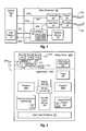
- FIG. 1schematically illustrates an example of an optical transceiver that may implement features of the present invention
- FIG. 2schematically illustrates an example of a control module of FIG. 1 ;
- FIG. 3illustrates configuration entry definitions that may be used to define configuration for various memory segments
- FIG. 4illustrates a method for configuring memory on a per-segment basis in accordance with the principles of the present invention.
- FIG. 5illustrates a block diagram of a set of hierarchal memory configuration tables including indexes in accordance with embodiments of the present invention.
- the principles of the present inventionrelate to a mechanism that enables an optical transceiver to configure system memory on a per-segment basis.
- the optical transceiverincludes a processing entity, system memory and a memory configuration table.
- the memory configuration tableis comprised of configuration entries, each of which defines the configuration setting for a corresponding segment of memory.
- the processing entityreads the configuration entry for a particular segment of the memory.
- the processing entitydetermines the set of one or more configuration settings for the memory segment based on the configuration entry read. The process may be repeated for multiple segments of memory.
- An example operational optical transceiver environmentwill first be described. Then, the operation in accordance with the invention will be described with respect to the operational environment.
- FIG. 1illustrates an optical transceiver 100 in which the principles of the present invention may be employed. While the optical transceiver 100 will be described in some detail, the optical transceiver 100 is described by way of illustration only, and not by way of restricting the scope of the invention.
- the principles of the present inventionare suitable for 1 G, 2 G, 4 G, 8 G, 10 G and higher bandwidth fiber optic links.
- the principles of the present inventionmay be implemented in optical (e.g., laser) transmitter/receivers of any form factor such as XFP, SFP and SFF, without restriction. Having said this, the principles of the present invention are not limited to an optical transceiver environment at all.
- the optical transceiver 100receives an optical signal from fiber 110 A using receiver 101 .
- the receiver 101acts as an opto-electric transducer by transforming the optical signal into an electrical signal.
- the receiver 101provides the resulting electrical signal to a post-amplifier 102 .
- the post-amplifier 102amplifies the signal and provides the amplified signal to an external host 111 as represented by arrow 102 A.
- the external host 111may be any computing system capable of communicating with the optical transceiver 100 .
- the external host 111may contain a host memory 112 that may be a volatile or non-volatile memory source.
- the optical transceiver 100may be a printed circuit board or other components/chips within the host 111 , although this is not required.
- the optical transceiver 100may also receive electrical signals from the host 111 for transmission onto the fiber 110 B.
- the laser driver 103receives the electrical signal as represented by the arrow 103 A, and drives the transmitter 104 (e.g., a laser or Light Emitting Diode (LED)) with signals that cause the transmitter 104 to emit onto the fiber 110 B optical signals representative of the information in the electrical signal provided by the host 111 .
- the transmitter 104serves as an electro-optic transducer.
- the optical transceiver 100includes a control module 105 , which may evaluate temperature and voltage conditions and other operational circumstances, and receive information from the post-amplifier 102 (as represented by arrow 105 A) and from the laser driver 103 (as represented by arrow 105 B). This allows the control module 105 to optimize the dynamically varying performance, and additionally detect when there is a loss of signal.
- control module 105may counteract these changes by adjusting settings on the post-amplifier 102 and/or the laser driver 103 as also represented by the arrows 105 A and 105 B. These settings adjustments are quite intermittent since they are only made when temperature or voltage or other low frequency changes so warrant. Receive power is an example of such a low frequency change.
- the control module 105may have access to a persistent memory 106 , which in one embodiment, is an Electrically Erasable and Programmable Read Only Memory (EEPROM).
- EEPROMElectrically Erasable and Programmable Read Only Memory
- the persistent memory 106 and the control module 105may be packaged together in the same package or in different packages without restriction.
- Persistent memory 106may also be any other non-volatile memory source.
- the control module 105includes both an analog portion 108 and a digital portion 109 . Together, they allow the control module to implement logic digitally, while still largely interfacing with the rest of the optical transceiver 100 using analog signals.
- FIG. 2schematically illustrates an example 200 of the control module 105 in further detail.
- the control module 200includes an analog portion 200 A that represents an example of the analog portion 108 of FIG. 1 , and a digital portion 200 B that represents an example of the digital portion 109 of FIG. 1 .
- the analog portion 200 Amay contain digital to analog converters, analog to digital converters, high speed comparators (e.g., for event detection), voltage based reset generators, voltage regulators, voltage references, clock generator, and other analog components.
- the analog portion 200 Aincludes sensors 211 A, 211 B, 211 C amongst potentially others as represented by the horizontal ellipses 211 D. Each of these sensors may be responsible for measuring operational parameters that may be measured from the control module 200 such as, for example, supply voltage and transceiver temperature.
- the control modulemay also receive external analog or digital signals from other components within the optical transceiver that indicate other measured parameters such as, for example, laser bias current, transmit power, receive power, laser wavelength, laser temperature, and Thermo Electric Cooler (TEC) current.
- TECThermo Electric Cooler
- Two external lines 212 A and 212 Bare illustrated for receiving such external analog signals although there may be many of such lines.
- the internal sensorsmay generate analog signals that represent the measured values.
- the externally provided signalsmay also be analog signals.
- the analog signalsare converted to digital signals so as to be available to the digital portion 200 B of the control module 200 for further processing.
- each analog parameter valuemay have its own Analog to Digital Converter (ADC).
- ADCAnalog to Digital Converter
- each signalmay be periodically sampled in a round robin fashion using a single ADC such as the illustrated ADC 214 .
- each analog valuemay be provided to a multiplexer 213 , which selects in a round robin fashion, one of the analog signals at a time for sampling by the ADC 214 .
- multiplexer 213may be programmed to allow any order of analog signals to be sampled by ADC 214 .
- the analog portion 200 A of the control module 200may also include other analog components 215 such as, for example, digital to analog converters, other analog to digital converters, high speed comparators (e.g., for event detection), voltage based reset generators, voltage regulators, voltage references, clock generator, and other analog components.
- the digital portion 200 B of the control module 200may include a timer module 202 that provides various timing signals used by the digital portion 200 B. Such timing signals may include, for example, programmable processor clock signals.
- the timer module 202may also act as a watchdog timer.
- Two general-purpose processors 203 A and 203 Bare also included.
- the processorsrecognize instructions that follow a particular instruction set, and may perform normal general-purpose operation such as shifting, branching, adding, subtracting, multiplying, dividing, Boolean operations, comparison operations, and the like.
- the general-purpose processors 203 A and 203 Bare each a 16-bit processor and may be identically structured.
- the precise structure of the instruction setis not important to the principles of the present invention as the instruction set may be optimized around a particular hardware environment, and as the precise hardware environment is not important to the principles of the present invention.
- a host communications interface 204is used to communicate with the host 111 , possibly implemented using a two-wire interface such as I 2 C shown in FIG. 1 as the serial data (SDA) and serial clock (SCL) lines on the optical transceiver 100 . Other host communication interfaces may also be implemented as well. Data may be provided from the control module 105 to the host 111 using this host communications interface to allow for digital diagnostics and readings of temperature levels, transmit/receiver power levels, and the like.
- the external device interface 205is used to communicate with, for example, other modules within the optical transceiver 100 such as, for example, the post-amplifier 102 , the laser driver 103 , or the persistent memory 106 .
- the internal controller system memory 206may be Random Access Memory (RAM) or non-volatile memory.
- the memory controller 207shares access to the controller system memory 206 amongst each of the processors 203 A and 203 B and with the host communication interface 204 and the external device interface 205 .
- the host communication interface 204includes a serial interface controller 201 A
- the external device interface 205includes a serial interface controller 201 B.
- the two serial interface controllers 201 A and 201 Bmay communicate using a two-wire interface such as I 2 C or may be another interface so long as the interface is recognized by both communicating modules.
- One serial interface controller(e.g., serial interface controller 201 B) is a master component, while the other serial interface controller (e.g., serial interface controller 201 A) is a slave component.
- An input/output multiplexer 208multiplexes the various input/output pins of the control module 200 to the various components within the control module 200 . This enables different components to dynamically assign pins in accordance with the then-existing operational circumstances of the control module 200 . Accordingly, there may be more input ⁇ output nodes within the control module 200 than there are pins available on the control module 200 , thereby reducing the footprint of the control module 200 .
- Register sets 209contain a number of individual registers. These registers may be used by the processors 203 to write microcode generated data that controls high speed comparison in optical transceiver 100 . Alternatively, the registers may hold data selecting operational parameters for comparison. Additionally, the registers may be memory mapped to the various components of optical transceiver 100 for controlling aspects of the component such as laser bias current or transmit power.
- system memorymay be controller system memory 206 and may be RAM as previously described, it may also be a processor, a register, a flip-flop, non-volatile memory (such as persistent memory 106 ), or any other memory device.
- the system memory or another memory locationsuch as a register in register sets 209 may contain a memory configuration table that is used by optical transceiver 100 to configure individual segments of the system memory.
- a memory configuration tablegives optical transceiver 100 the ability to configure large portions of the system memory (potentially the entire system memory) while only utilizing a very small portion of the memory for the configuration process.
- the memory configuration tableallows the flexibility to configure different size memory segments for different purposes. The table removes the need to configure large portions of memory as single use segments.
- the memory configuration tablemay be single table or it may consist of multiple tables.
- the memory configuration tablecontains memory configuration entries that define the address and configuration settings for a given segment of memory. Examples of configuration settings are readable memory, writeable memory, non-volatile memory, volatile memory, and processor interrupt.
- an example definition 300 for how the configuration entry may be structured to define various configuration settingsis shown.
- This example definition 300is by way of illustration only, and it is contemplated that there are numerous additional ways to implement a memory configuration entry on a memory configuration table.
- Memory configuration definition 300is shown as a one byte (eight-bit) entry, although this is not required.
- Memory configuration entry portion 300is comprised of various configuration setting possibilities 310 .
- the configuration settings 310correspond to the various ways that a memory segment may be configured.
- An abbreviation table 320is also shown that defines abbreviations for the configuration settings 310 that will be used in subsequent figures.
- the seventh (M 6 ) and sixth (M 5 ) bits of memory configuration entry 300are used to configure memory type for a given segment of memory.
- the seventh bit M 6defines whether processor attention is required (using, for example, a processor interrupt) when interfacing with that memory segment.
- a binary zero for bit M 6indicates that no processor interrupt is used.
- bit M 5identifies the type of memory, with a binary zero for M 5 indicating that the memory is to be treated as non-volatile memory, and with a binary one for M 5 indicating that the memory is to be treated as volatile memory.
- a binary one for bit M 6indicates that a processor interrupt is used. In that case (M 6 being one), bit M 5 determines various processor attention states or interrupts that are used to provide different levels of priority for providing an interrupt to a processor.
- the fourth (R 3 ) and third (R 2 ) bitsare used to configure different levels of access permission needed to read the memory segment. For instance, if R 3 is zero and R 2 is zero, no password is needed to read the memory segment. If R 3 is zero and R 2 is one, read permission may be obtained using any one of three passwords (referred to herein as “password 1”, “password 2” and “password 3”). If R 3 is one and R 2 is zero, read permission may be obtained by using two of the higher level passwords (e.g., password 2 or 3). If R 3 is one and R 2 is one, read permission may be obtained by using only the highest level password (e.g., password 3). Accordingly, the memory segments may be configured by implementing a four level password scheme for allowing a host computing system access to the readable segment of memory.
- the second (W 1 ) and first (W 0 ) bitsare used to configure a segment of memory as writeable using the same four level password scheme.
- the same principles as discussed for the read bitsapply to the write bits (i.e., there are two bits with four different combinations of binary ones and zeros possible). It is possible to independently configure a memory segment to be both readable and writeable for different password levels.
- FIG. 3also shows an eighth bit (E 7 ) and a fifth bit (D 4 ).
- Bit E 7may be used by embodiments that implement multiple memory configuration tables to identify the memory configuration table.
- one portion of system memoryis utilized by one device, and a second portion of system memory is utilized by a second device.
- Bit D 4identifies which of the two devices the memory location corresponds to.
- the two devicesmay be different I2C devices controlled by different host interfaces. For example, D0 may correspond to the first I2C device and D1 may correspond to the second I2C device.
- a processing entityreads a first configuration entry in a memory configuration table corresponding to a first memory segment of controller system memory 206 (act 401 ).
- processing entityis defined to mean a microprocessor such as a processor 203 , a state machine, or any other processing device capable of reading a configuration table.
- the configuration entrydefines a set of one or more configuration settings such as read and write for the memory segment.
- first”, “second” and so forth to modify a configuration entry or a memory segmentis not intended to represent any sequential, temporal or spatial ordering of the configuration entries or memory segments, but is used merely to distinguish one configuration entry or memory segment from another.
- the processing entitydetermines configuration settings for the first memory segment based on the configuration entry read (act 402 ). For example, the processing entity may read in the memory configuration entry that the memory segment is readable without a password and corresponds to a processor interrupt should a write occur. The processing entity uses the reading to configure the system to cause a processor interrupt to be generated to the identified processor should a write to the memory segment occur. Should a request to read the memory segment be received, these configuration settings may be used to determine that the reading should be allowed without any password requirements.
- the processing entitymay read a second configuration entry in the memory configuration table corresponding to a second segment of controller system memory 206 (act 403 ).
- the configuration entrydefines a set of configuration settings for the second memory segment that may be different from the set of configuration settings for the first segment of memory.
- the processing entitydetermines configuration settings for the second memory segment based on the second configuration entry read (act 404 ). For example, the processing entity may read in the memory configuration entry a configuration setting for writeable memory. The processing entity uses the reading to configure the memory segment to be writable. Although only described for two memory segments, the method may also be performed on as many segments of system memory (as represented by the vertical ellipses 405 ) for which there is a corresponding memory configuration entry in the memory configuration table.
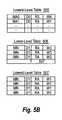
- a memory configuration tablethat comprises multiple tables. These multiple tables may be implemented as a plurality of hierarchical tables.
- the plurality of hierarchical tablesincludes one or more lower-level tables.
- a main tableincludes indexes that index into the lower-level tables.
- the lower-level tablesmay have indexes that index into additional lower-level tables.
- the lower-level tableshave increasing granularity in that each configuration entry corresponds to a smaller and smaller amount of system memory. In this way, it is possible to configure each segment of system memory on a byte-by-byte basis (or even perhaps a bit-by-bit basis) if necessary.
- FIG. 5(represented as FIGS. 5A and 5B due to the size of the hierarchical tables), an example set of hierarchical tables 500 is shown by way of illustration only and should not be read to limit any claims.
- a main table 501covers the entire system memory, or at least the entire portion that is configurable. In this example, the configurable, memory is approximately 2K bytes.
- the memory configuration abbreviations 320 of FIG. 3are used in the figures to depict the configuration settings.
- main table 501there are sixteen entries shown, each covering a memory segment of 128 bytes. All entries but the first and sixteenth entries have configuration settings shown that indicate that the memory segments are non-volatile memory (i.e., “MN”), cover device one (i.e., “D0”), and are both readable and writeable using password 3 (i.e., “R3” and “W3”). These main entries require relatively little configuration information since four bytes of configuration information may be used to define configuration for the 128 byte segments. Of course, the size of the segments may be much larger including entire kilobytes, megabytes, or gigabytes, or so forth.
- MNnon-volatile memory
- D0cover device one
- password 3i.e., “R3” and “W3”.
- the first and sixteenth entriescontain an index that indexes into lower-level tables having more refined granularity.
- the first entry of main table 501 into lower-level table 502 while the sixteenth entry of the main tableindexes into lower level table 506 .
- Lower-level table 502has four entries that define configuration for memory segments that are 32 bytes in size.
- the configuration settingsindicate that the memory segments are non-volatile memory, cover device one, and are both readable by all (i.e., “RA”) and writeable by password 1 (i.e., “W1”).
- the fourth entrycontains an index to an even lower-level table 503 having even more refined granularity.
- lower-level table 503has four entries that define configuration for memory segments that are only eight bytes in size.
- the configuration settingsindicate that the memory segments are non-volatile memory, cover device one, and are both readable by all and writeable by password 3.
- the fourth entrycontains an index to a lower-level table 504 having more refined granularity.
- Lower-level table 504has four entries that define configuration for memory segments that are only two bytes in size. These entries also require relatively high configuration information since four bytes of configuration information may be used to define configuration for the two byte segments. In this case the configuration settings indicate memory segments that are volatile memory, cover device one, are readable by password 3, and are writeable by all (i.e., “WA”). However, the fourth entry contains an index to a lowest-level table 505 having very refined granularity of just one byte.
- Lowest-level table 505has two entries that define configuration for memory segments that are a mere one byte in size. These entries require the highest level of configuration information since four bytes of configuration information is used to define configuration for the one byte segments.
- the first entryhas configuration settings indicating a memory segment that produces a processor interrupt whenever the memory segment is written to or read (i.e., “MA0”), is readable by password 3, and is writable by all.
- the second entryhas configuration settings indicating a memory segment that produces a processor interrupt whenever the memory segment is written to or read (i.e., “MA1”), is readable by all, and is writable by password 1.
- lower-level table 506has four entries that cover segments of memory that are 32 bytes.
- the first three entriescontain configuration settings that indicate the configurations for the entire 32 bytes of memory.
- the configuration settingsindicate memory segments that are non-volatile memory, cover device two (i.e., “D1”), are readable by all, and are writeable by password 3.
- the fourth entrycontains an index to a lower-level table 507 having more refined granularity.
- Lowest-level 507has four entries that cover segments of memory that are eight bytes.
- the entriescontain configuration settings that indicate the configurations for the entire eight bytes of memory.
- the configuration settingsindicate memory segments that are non-volatile memory, cover device two, and are both readable by all and writeable by password 1.
- the hierarchal table just describedis only one of countless ways that a hierarchal table system may be implemented.
- One of skill in the artwill appreciate the versatility that this type of system provides in determining the size and number of the individual tables, the size of the memory segments covered by individual configuration entries and so on.
- the hierarchal tablesallow the configuration of the system memory on a per-segment basis down to a single byte if desired, or even further.
- a segment of memorymay be configured by optical transceiver 100 to be non-volatile memory.
- the optical transceiver 100after determining that the segment is non-volatile, may direct that any data written to the memory segment be written back to a persistent memory source such as persistent memory 106 .
- the data that is writtenmay be stored in both volatile (such as controller system memory 206 ) and non-volatile memory.
- the memory configuration tablemay contain a configuration entry with configuration settings that indicate that a particular segment of memory is non-volatile and writable.
- a processing entitywould read the configuration entry and the corresponding configuration settings as described. The processing entity would then configure the memory segment to be non-volatile memory and writable.
- a segment of memorymay be configured by optical transceiver 100 to produce a processor interrupt.
- the processor interruptmay be generated for a segment of memory that is configured to produce an interrupt when a portion of the segment has been overwritten in an undesired manner.
- the processor interruptmay also be generated when a segment of memory has been read by an unauthorized party.
- the processorin such cases, may stop all other activities and proceed to restore the memory segment to it original value by writing new data to the memory segment or by initiating a warm reboot.
- the interruptsmay be an important safeguard for memory segments containing sensitive data.
- two processorssuch as the embodiment of FIG.
- both processorsmay be independently configured to enable either of the interrupts or both of the interrupts.
- processor 203 Amay be configured to enable only MA0, only MA1, or both MA0 and MA1.
- Processor 203 Bmay be enabled in like manner.
- the principles of the present inventionrelate to configuring memory on a per-segment basis.
- a memory configuration tableis utilized, allowing the configuration of large portions of memory while only using a very small amount of memory for the table.
- different size memory segmentsmay be configured for different purposes. These segments may later be reconfigured by changing configuration settings contained in the configuration table.
- the memory segmentsmay be configured on a byte level if necessary. This leads to an efficient use of limited memory resources. Accordingly, the principles of the present invention are a significant advancement in the art of configuring memory in optical transceivers.
Landscapes
- Engineering & Computer Science (AREA)
- Theoretical Computer Science (AREA)
- Physics & Mathematics (AREA)
- Computer Security & Cryptography (AREA)
- General Engineering & Computer Science (AREA)
- General Physics & Mathematics (AREA)
- Mathematical Physics (AREA)
- Optical Communication System (AREA)
Abstract
Description
Claims (20)
Priority Applications (1)
| Application Number | Priority Date | Filing Date | Title |
|---|---|---|---|
| US11/074,109US8090265B2 (en) | 2004-03-05 | 2005-03-07 | Byte-configurable memory in an optical transceiver |
Applications Claiming Priority (2)
| Application Number | Priority Date | Filing Date | Title |
|---|---|---|---|
| US55054404P | 2004-03-05 | 2004-03-05 | |
| US11/074,109US8090265B2 (en) | 2004-03-05 | 2005-03-07 | Byte-configurable memory in an optical transceiver |
Publications (2)
| Publication Number | Publication Date |
|---|---|
| US20050238359A1 US20050238359A1 (en) | 2005-10-27 |
| US8090265B2true US8090265B2 (en) | 2012-01-03 |
Family
ID=34975765
Family Applications (2)
| Application Number | Title | Priority Date | Filing Date |
|---|---|---|---|
| US11/073,827Active2026-10-29US8200095B2 (en) | 2004-03-05 | 2005-03-07 | Multi-level memory access in an optical transceiver |
| US11/074,109Active2029-03-13US8090265B2 (en) | 2004-03-05 | 2005-03-07 | Byte-configurable memory in an optical transceiver |
Family Applications Before (1)
| Application Number | Title | Priority Date | Filing Date |
|---|---|---|---|
| US11/073,827Active2026-10-29US8200095B2 (en) | 2004-03-05 | 2005-03-07 | Multi-level memory access in an optical transceiver |
Country Status (4)
| Country | Link |
|---|---|
| US (2) | US8200095B2 (en) |
| EP (1) | EP1723530A4 (en) |
| CN (1) | CN100418074C (en) |
| WO (1) | WO2005088462A1 (en) |
Cited By (1)
| Publication number | Priority date | Publication date | Assignee | Title |
|---|---|---|---|---|
| US20050196165A1 (en)* | 2004-03-05 | 2005-09-08 | Finisar Corporation | Multi-level memory access in an optical transceiver |
Families Citing this family (15)
| Publication number | Priority date | Publication date | Assignee | Title |
|---|---|---|---|---|
| US7848644B2 (en) | 2004-02-23 | 2010-12-07 | Dynamic Method Enterprises Limited | Method and an apparatus to provide optical equipment protection |
| US7130950B1 (en)* | 2004-04-30 | 2006-10-31 | Hewlett-Packard Development Company, Lp. | Providing access to memory configuration information in a computer |
| US7509441B1 (en) | 2006-06-30 | 2009-03-24 | Siliconsystems, Inc. | Systems and methods for segmenting and protecting a storage subsystem |
| US7447807B1 (en)* | 2006-06-30 | 2008-11-04 | Siliconsystems, Inc. | Systems and methods for storing data in segments of a storage subsystem |
| US8549236B2 (en) | 2006-12-15 | 2013-10-01 | Siliconsystems, Inc. | Storage subsystem with multiple non-volatile memory arrays to protect against data losses |
| US8825940B1 (en) | 2008-12-02 | 2014-09-02 | Siliconsystems, Inc. | Architecture for optimizing execution of storage access commands |
| US9176859B2 (en)* | 2009-01-07 | 2015-11-03 | Siliconsystems, Inc. | Systems and methods for improving the performance of non-volatile memory operations |
| US10079048B2 (en)* | 2009-03-24 | 2018-09-18 | Western Digital Technologies, Inc. | Adjusting access of non-volatile semiconductor memory based on access time |
| JP2012169745A (en)* | 2011-02-10 | 2012-09-06 | Sumitomo Electric Ind Ltd | Optical transceiver |
| US9147195B2 (en)* | 2011-06-14 | 2015-09-29 | Microsoft Technology Licensing, Llc | Data custodian and curation system |
| US9244956B2 (en) | 2011-06-14 | 2016-01-26 | Microsoft Technology Licensing, Llc | Recommending data enrichments |
| US8812764B2 (en) | 2011-10-28 | 2014-08-19 | Sumitomo Electric Industries, Ltd. | Apparatus installing devices controlled by MDIO or SPI protocol and method to control the same |
| US8882366B2 (en)* | 2011-12-07 | 2014-11-11 | Finisar Corporation | Chip identification pads for identification of integrated circuits in an assembly |
| US9292713B2 (en)* | 2013-03-13 | 2016-03-22 | Intel Corporation | Tiered access to on chip features |
| TW202209323A (en) | 2020-02-14 | 2022-03-01 | 美商爾雅實驗室公司 | Remote memory architectures enabled by monolithic in-package optical i/o |
Citations (50)
| Publication number | Priority date | Publication date | Assignee | Title |
|---|---|---|---|---|
| US5524243A (en)* | 1992-12-16 | 1996-06-04 | Rolm Company | Parallel programming of field programmable gate array devices |
| US5822749A (en) | 1994-07-12 | 1998-10-13 | Sybase, Inc. | Database system with methods for improving query performance with cache optimization strategies |
| US5892922A (en)* | 1997-02-28 | 1999-04-06 | 3Com Corporation | Virtual local area network memory access system |
| US5912897A (en)* | 1996-01-31 | 1999-06-15 | Siemens Aktiengesellschaft | Method for converting messages exhibiting different formats in communication systems |
| US5956168A (en)* | 1997-08-14 | 1999-09-21 | Finisar Corporation | Multi-protocol dual fiber link laser diode controller and method |
| US5978952A (en) | 1996-12-31 | 1999-11-02 | Intel Corporation | Time-distributed ECC scrubbing to correct memory errors |
| US6012109A (en)* | 1997-09-09 | 2000-01-04 | National Instruments Corporation | Video capture device with adjustable frame rate based on available bus bandwidth |
| US6032160A (en)* | 1995-02-10 | 2000-02-29 | International Business Machines Corporation | Buddy system space allocation management |
| US6076183A (en) | 1997-12-18 | 2000-06-13 | Bull, S.A. | Method of memory error correction by scrubbing |
| US6259702B1 (en)* | 1996-10-18 | 2001-07-10 | Canon Kabushiki Kaisha | Server system for delivering signal and delivery method of signal therein |
| US20020016942A1 (en) | 2000-01-26 | 2002-02-07 | Maclaren John M. | Hard/soft error detection |
| US6378023B1 (en)* | 1996-02-14 | 2002-04-23 | Advanced Micro Devices, Inc. | Interrupt descriptor cache for a microprocessor |
| US20020080798A1 (en)* | 2000-06-30 | 2002-06-27 | Yoichi Hariguchi | Network routing table and packet routing method |
| US6446145B1 (en) | 2000-01-06 | 2002-09-03 | International Business Machines Corporation | Computer memory compression abort and bypass mechanism when cache write back buffer is full |
| US6535743B1 (en)* | 1998-07-29 | 2003-03-18 | Minorplanet Systems Usa, Inc. | System and method for providing directions using a communication network |
| US20030097608A1 (en)* | 2001-11-20 | 2003-05-22 | Rodeheffer Thomas Lee | System and method for scrubbing errors in very large memories |
| US20030177319A1 (en)* | 2002-03-18 | 2003-09-18 | Sun Microsystems, Inc. A Delaware Corporation | Enhanced memory management for portable devices |
| US6643818B1 (en) | 1999-11-19 | 2003-11-04 | International Business Machines Corporation | Storing and using the history of data transmission errors to assure data integrity |
| US20030208658A1 (en)* | 2002-05-06 | 2003-11-06 | Sony Computer Entertainment America Inc. | Methods and apparatus for controlling hierarchical cache memory |
| US6658437B1 (en)* | 2000-06-05 | 2003-12-02 | International Business Machines Corporation | System and method for data space allocation using optimized bit representation |
| US20030229765A1 (en) | 2001-03-22 | 2003-12-11 | Sony Computer Entertainment Inc. | Memory protection system and method for computer architecture for broadband networks |
| US20040022537A1 (en) | 2001-01-24 | 2004-02-05 | Fsona Communiations Corporation | Laser communication system |
| US20040081424A1 (en)* | 2002-10-29 | 2004-04-29 | Mitsubishi Denki Kabushiki Kaisha | Transceiver integrated circuit and communication module |
| US20040126111A1 (en)* | 2002-12-27 | 2004-07-01 | Cho Yun-Hee | System and method for operating optical transponder |
| US20040132956A1 (en)* | 2001-01-18 | 2004-07-08 | Toshikazu Hamao | Thermosetting resin composition for vacuum, method for manufacturing the same, and vacuum device using the same |
| US20040136722A1 (en)* | 2003-01-15 | 2004-07-15 | Mahowald Peter H. | Calibrating an optical transceiver via adaptive testing |
| US20040136719A1 (en)* | 2003-01-15 | 2004-07-15 | Takashi Hidai | EEPROM emulation in a transceiver |
| US6775781B1 (en) | 1999-12-13 | 2004-08-10 | Microsoft Corporation | Administrative security systems and methods |
| US20040162079A1 (en)* | 2002-12-02 | 2004-08-19 | Ntt Docomo, Inc. | Radio access network system, radio communication method, control server and data server |
| US20040162956A1 (en) | 2003-02-18 | 2004-08-19 | Takashi Hidai | System and method for implementing a hidden address in a communication module |
| US20040202476A1 (en)* | 2003-04-09 | 2004-10-14 | Woolf Kevin Reid | Tables for determining the signal strength of a received signal in a fibre optics transceiver |
| US6826658B1 (en)* | 2002-06-20 | 2004-11-30 | Xilinx, Inc. | Method and apparatus for managing an optical transceiver |
| US6925546B2 (en)* | 2002-12-02 | 2005-08-02 | Wind River Systems, Inc. | Memory pool configuration system |
| US20050196165A1 (en)* | 2004-03-05 | 2005-09-08 | Finisar Corporation | Multi-level memory access in an optical transceiver |
| US6981125B2 (en)* | 2003-04-22 | 2005-12-27 | International Business Machines Corporation | Method and apparatus for managing shared virtual storage in an information handling system |
| US6983355B2 (en)* | 2003-06-09 | 2006-01-03 | International Business Machines Corporation | Virtualization of physical storage using size optimized hierarchical tables |
| US20060007905A1 (en) | 2004-03-23 | 2006-01-12 | Yach David P | System and method for recovering from a software processing error |
| US20060034612A1 (en)* | 2003-12-19 | 2006-02-16 | Rangchen Yu | Multi-data-rate optical transceiver |
| US20060147216A1 (en) | 2004-12-30 | 2006-07-06 | Dybsetter Gerald L | Background consistency checking in an optical transceiver |
| US20060193631A1 (en)* | 2005-02-25 | 2006-08-31 | Gilligan Douglas A | Inter-module communications of an optical network element |
| US20060198635A1 (en)* | 2005-03-04 | 2006-09-07 | Emery Clayton J | Optical network terminal with illegal transmission detection circuitry |
| US7158477B2 (en)* | 2001-12-20 | 2007-01-02 | Nortel Networks Limited | Data communication apparatus with distributed traffic protection switching system |
| US20070002773A1 (en) | 2002-07-10 | 2007-01-04 | Yongchang Wang | Redundant multi-fiber optical ring network |
| US20070079185A1 (en) | 2005-09-19 | 2007-04-05 | Totolos George Jr | Memory scrubbing of expanded memory |
| US7215891B1 (en)* | 2003-06-06 | 2007-05-08 | Jds Uniphase Corporation | Integrated driving, receiving, controlling, and monitoring for optical transceivers |
| US7233998B2 (en) | 2001-03-22 | 2007-06-19 | Sony Computer Entertainment Inc. | Computer architecture and software cells for broadband networks |
| US7289045B1 (en)* | 2006-06-21 | 2007-10-30 | Honeywell International Inc. | Two-stage codec for frame-based program images |
| US7296127B2 (en) | 2003-03-31 | 2007-11-13 | Intel Corporation | NoDMA cache |
| US7570887B2 (en) | 2003-03-31 | 2009-08-04 | Lockheed Martin Corporation | Optical network interface systems and devices |
| US7801449B2 (en)* | 2004-09-07 | 2010-09-21 | Finisar Corporation | Off-module optical transceiver firmware paging |
Family Cites Families (18)
| Publication number | Priority date | Publication date | Assignee | Title |
|---|---|---|---|---|
| US4937736A (en)* | 1987-11-30 | 1990-06-26 | International Business Machines Corporation | Memory controller for protected memory with automatic access granting capability |
| US5619671A (en)* | 1993-04-19 | 1997-04-08 | International Business Machines Corporation | Method and apparatus for providing token controlled access to protected pages of memory |
| US6259703B1 (en)* | 1993-10-22 | 2001-07-10 | Mitel Corporation | Time slot assigner for communication system |
| CN1162788A (en)* | 1995-12-29 | 1997-10-22 | 国际商业机器公司 | System and method for controlling access to protected objects in an object-oriented system |
| JP3764517B2 (en)* | 1996-01-26 | 2006-04-12 | 株式会社ルネサステクノロジ | Communication device |
| US6826369B1 (en)* | 1999-04-23 | 2004-11-30 | System To Asic, Inc. | Intelligent sensor platform |
| GB2366888A (en)* | 2000-04-14 | 2002-03-20 | Ibm | Restricting data access to data in data processing systems |
| US7079775B2 (en)* | 2001-02-05 | 2006-07-18 | Finisar Corporation | Integrated memory mapped controller circuit for fiber optics transceiver |
| US7043640B2 (en)* | 2001-02-14 | 2006-05-09 | Pritchard James B | Apparatus and method for protecting a computer system |
| US6554492B2 (en)* | 2001-06-01 | 2003-04-29 | Stratos Lightwave | Addressable transceiver module |
| US7739498B2 (en)* | 2002-01-15 | 2010-06-15 | GlobalFoundries, Inc. | Method and apparatus for multi-table accessing of input/output devices using target security |
| SE0200812L (en)* | 2002-03-18 | 2003-09-16 | Optillion Ab | communication Module |
| US6836493B2 (en)* | 2003-01-15 | 2004-12-28 | Agilent Technologies, Inc. | Laser initialization in firmware controlled optical transceiver |
| US20050015540A1 (en)* | 2003-07-18 | 2005-01-20 | Hung-Chou Tsai | Auto-executable portable data storage device and the method of auto-execution thereof |
| US7974538B2 (en)* | 2004-10-29 | 2011-07-05 | Finisar Corporation | Transaction for transceiver firmware download |
| US7957651B2 (en)* | 2004-10-29 | 2011-06-07 | Finisar Corporation | Configurable optical transceiver feature specific cost transaction |
| US7295750B2 (en)* | 2004-12-30 | 2007-11-13 | Finisar Corporation | Access key enabled update of an optical transceiver |
| US7881615B2 (en)* | 2007-07-26 | 2011-02-01 | Finisar Corporation | Dynamic digital diagnostic alerts |
- 2005
- 2005-03-07WOPCT/US2005/007267patent/WO2005088462A1/enactiveApplication Filing
- 2005-03-07EPEP05724750Apatent/EP1723530A4/ennot_activeWithdrawn
- 2005-03-07USUS11/073,827patent/US8200095B2/enactiveActive
- 2005-03-07USUS11/074,109patent/US8090265B2/enactiveActive
- 2005-03-07CNCNB2005800071788Apatent/CN100418074C/ennot_activeExpired - Fee Related
Patent Citations (52)
| Publication number | Priority date | Publication date | Assignee | Title |
|---|---|---|---|---|
| US5524243A (en)* | 1992-12-16 | 1996-06-04 | Rolm Company | Parallel programming of field programmable gate array devices |
| US5822749A (en) | 1994-07-12 | 1998-10-13 | Sybase, Inc. | Database system with methods for improving query performance with cache optimization strategies |
| US6032160A (en)* | 1995-02-10 | 2000-02-29 | International Business Machines Corporation | Buddy system space allocation management |
| US5912897A (en)* | 1996-01-31 | 1999-06-15 | Siemens Aktiengesellschaft | Method for converting messages exhibiting different formats in communication systems |
| US6378023B1 (en)* | 1996-02-14 | 2002-04-23 | Advanced Micro Devices, Inc. | Interrupt descriptor cache for a microprocessor |
| US6259702B1 (en)* | 1996-10-18 | 2001-07-10 | Canon Kabushiki Kaisha | Server system for delivering signal and delivery method of signal therein |
| US5978952A (en) | 1996-12-31 | 1999-11-02 | Intel Corporation | Time-distributed ECC scrubbing to correct memory errors |
| US5892922A (en)* | 1997-02-28 | 1999-04-06 | 3Com Corporation | Virtual local area network memory access system |
| US5956168A (en)* | 1997-08-14 | 1999-09-21 | Finisar Corporation | Multi-protocol dual fiber link laser diode controller and method |
| US6012109A (en)* | 1997-09-09 | 2000-01-04 | National Instruments Corporation | Video capture device with adjustable frame rate based on available bus bandwidth |
| US6076183A (en) | 1997-12-18 | 2000-06-13 | Bull, S.A. | Method of memory error correction by scrubbing |
| US6535743B1 (en)* | 1998-07-29 | 2003-03-18 | Minorplanet Systems Usa, Inc. | System and method for providing directions using a communication network |
| US6643818B1 (en) | 1999-11-19 | 2003-11-04 | International Business Machines Corporation | Storing and using the history of data transmission errors to assure data integrity |
| US6775781B1 (en) | 1999-12-13 | 2004-08-10 | Microsoft Corporation | Administrative security systems and methods |
| US6446145B1 (en) | 2000-01-06 | 2002-09-03 | International Business Machines Corporation | Computer memory compression abort and bypass mechanism when cache write back buffer is full |
| US20020016942A1 (en) | 2000-01-26 | 2002-02-07 | Maclaren John M. | Hard/soft error detection |
| US6658437B1 (en)* | 2000-06-05 | 2003-12-02 | International Business Machines Corporation | System and method for data space allocation using optimized bit representation |
| US20020080798A1 (en)* | 2000-06-30 | 2002-06-27 | Yoichi Hariguchi | Network routing table and packet routing method |
| US20040132956A1 (en)* | 2001-01-18 | 2004-07-08 | Toshikazu Hamao | Thermosetting resin composition for vacuum, method for manufacturing the same, and vacuum device using the same |
| US20040022537A1 (en) | 2001-01-24 | 2004-02-05 | Fsona Communiations Corporation | Laser communication system |
| US20030229765A1 (en) | 2001-03-22 | 2003-12-11 | Sony Computer Entertainment Inc. | Memory protection system and method for computer architecture for broadband networks |
| US7233998B2 (en) | 2001-03-22 | 2007-06-19 | Sony Computer Entertainment Inc. | Computer architecture and software cells for broadband networks |
| US20030097608A1 (en)* | 2001-11-20 | 2003-05-22 | Rodeheffer Thomas Lee | System and method for scrubbing errors in very large memories |
| US7158477B2 (en)* | 2001-12-20 | 2007-01-02 | Nortel Networks Limited | Data communication apparatus with distributed traffic protection switching system |
| US20030177319A1 (en)* | 2002-03-18 | 2003-09-18 | Sun Microsystems, Inc. A Delaware Corporation | Enhanced memory management for portable devices |
| US20030208658A1 (en)* | 2002-05-06 | 2003-11-06 | Sony Computer Entertainment America Inc. | Methods and apparatus for controlling hierarchical cache memory |
| US6826658B1 (en)* | 2002-06-20 | 2004-11-30 | Xilinx, Inc. | Method and apparatus for managing an optical transceiver |
| US20070002773A1 (en) | 2002-07-10 | 2007-01-04 | Yongchang Wang | Redundant multi-fiber optical ring network |
| US20040081424A1 (en)* | 2002-10-29 | 2004-04-29 | Mitsubishi Denki Kabushiki Kaisha | Transceiver integrated circuit and communication module |
| US20040162079A1 (en)* | 2002-12-02 | 2004-08-19 | Ntt Docomo, Inc. | Radio access network system, radio communication method, control server and data server |
| US6925546B2 (en)* | 2002-12-02 | 2005-08-02 | Wind River Systems, Inc. | Memory pool configuration system |
| US20040126111A1 (en)* | 2002-12-27 | 2004-07-01 | Cho Yun-Hee | System and method for operating optical transponder |
| US20040136722A1 (en)* | 2003-01-15 | 2004-07-15 | Mahowald Peter H. | Calibrating an optical transceiver via adaptive testing |
| US20040136719A1 (en)* | 2003-01-15 | 2004-07-15 | Takashi Hidai | EEPROM emulation in a transceiver |
| US20040162956A1 (en) | 2003-02-18 | 2004-08-19 | Takashi Hidai | System and method for implementing a hidden address in a communication module |
| US7570887B2 (en) | 2003-03-31 | 2009-08-04 | Lockheed Martin Corporation | Optical network interface systems and devices |
| US7296127B2 (en) | 2003-03-31 | 2007-11-13 | Intel Corporation | NoDMA cache |
| US20040202476A1 (en)* | 2003-04-09 | 2004-10-14 | Woolf Kevin Reid | Tables for determining the signal strength of a received signal in a fibre optics transceiver |
| US6981125B2 (en)* | 2003-04-22 | 2005-12-27 | International Business Machines Corporation | Method and apparatus for managing shared virtual storage in an information handling system |
| US7215891B1 (en)* | 2003-06-06 | 2007-05-08 | Jds Uniphase Corporation | Integrated driving, receiving, controlling, and monitoring for optical transceivers |
| US6983355B2 (en)* | 2003-06-09 | 2006-01-03 | International Business Machines Corporation | Virtualization of physical storage using size optimized hierarchical tables |
| US20060034612A1 (en)* | 2003-12-19 | 2006-02-16 | Rangchen Yu | Multi-data-rate optical transceiver |
| WO2005088462A1 (en) | 2004-03-05 | 2005-09-22 | Finisar Corporation | Hierarchical and byte-configurable memory in an optical transceiver |
| US20050196165A1 (en)* | 2004-03-05 | 2005-09-08 | Finisar Corporation | Multi-level memory access in an optical transceiver |
| US20060007905A1 (en) | 2004-03-23 | 2006-01-12 | Yach David P | System and method for recovering from a software processing error |
| US7801449B2 (en)* | 2004-09-07 | 2010-09-21 | Finisar Corporation | Off-module optical transceiver firmware paging |
| US20060147216A1 (en) | 2004-12-30 | 2006-07-06 | Dybsetter Gerald L | Background consistency checking in an optical transceiver |
| US20060193631A1 (en)* | 2005-02-25 | 2006-08-31 | Gilligan Douglas A | Inter-module communications of an optical network element |
| US7441061B2 (en)* | 2005-02-25 | 2008-10-21 | Dynamic Method Enterprises Limited | Method and apparatus for inter-module communications of an optical network element |
| US20060198635A1 (en)* | 2005-03-04 | 2006-09-07 | Emery Clayton J | Optical network terminal with illegal transmission detection circuitry |
| US20070079185A1 (en) | 2005-09-19 | 2007-04-05 | Totolos George Jr | Memory scrubbing of expanded memory |
| US7289045B1 (en)* | 2006-06-21 | 2007-10-30 | Honeywell International Inc. | Two-stage codec for frame-based program images |
Non-Patent Citations (12)
| Title |
|---|
| U.S. Appl. No. 11/073, 886, filed Mar. 7, 2005 entitled "Consistency Checking Over Internal Information in an Optical Transceiver". |
| U.S. Appl. No. 11/073,827, filed Dec. 21, 2009, Office Action. |
| U.S. Appl. No. 11/073,827, filed Feb. 2, 2011, Office Action. |
| U.S. Appl. No. 11/073,827, filed Jul. 6, 2010, Office Action. |
| U.S. Appl. No. 11/073,827, filed Jun. 26, 2008, Office Action. |
| U.S. Appl. No. 11/073,827, filed Jun. 26, 2009, Office Action. |
| U.S. Appl. No. 11/073,827, filed Mar. 7, 2005 entitled "Multi-Level Memory Access in an Optical Transceiver.". |
| U.S. Appl. No. 11/073,827, filed Nov. 9, 2007, Office Action. |
| U.S. Appl. No. 11/073,827, filed Oct. 29, 2008, Office Action. |
| U.S. Appl. No. 11/073,886, filed Apr. 8, 2008, Office Action. |
| U.S. Appl. No. 11/073,886, filed Nov. 20, 2008, Office Action. |
| U.S. Appl. No. 11/073,886, filed Sep. 20, 2007, Office Action. |
Cited By (2)
| Publication number | Priority date | Publication date | Assignee | Title |
|---|---|---|---|---|
| US20050196165A1 (en)* | 2004-03-05 | 2005-09-08 | Finisar Corporation | Multi-level memory access in an optical transceiver |
| US8200095B2 (en)* | 2004-03-05 | 2012-06-12 | Finisar Corporation | Multi-level memory access in an optical transceiver |
Also Published As
| Publication number | Publication date |
|---|---|
| US8200095B2 (en) | 2012-06-12 |
| US20050196165A1 (en) | 2005-09-08 |
| CN100418074C (en) | 2008-09-10 |
| WO2005088462A1 (en) | 2005-09-22 |
| CN1930556A (en) | 2007-03-14 |
| US20050238359A1 (en) | 2005-10-27 |
| EP1723530A4 (en) | 2008-12-31 |
| EP1723530A1 (en) | 2006-11-22 |
Similar Documents
| Publication | Publication Date | Title |
|---|---|---|
| US8090265B2 (en) | Byte-configurable memory in an optical transceiver | |
| US8582974B2 (en) | Inter-transceiver module communication for firmware upgrade | |
| US7908406B2 (en) | Interface architecture for facilitating communication regardless of protocol | |
| WO2009042301A1 (en) | Asymmetric scheduling of multiple analog inputs using a single a/d converter for fiber-optic transceivers | |
| WO2006116504A2 (en) | Changing transceiver module device addresses using a single host interface | |
| US7533254B2 (en) | Volatile memory persistence during warm reboot in an optical transceiver | |
| US7295750B2 (en) | Access key enabled update of an optical transceiver | |
| US8086892B2 (en) | Microcode configurable frequency clock | |
| US20060147215A1 (en) | Host printed circuit board with multiple optical transceivers | |
| US20060147217A1 (en) | Self-testing optical transceiver controller using internalized loopbacks | |
| US7522840B2 (en) | Adjustable boot speed in an optical transceiver | |
| US7957649B2 (en) | Module command interface for an optical transceiver | |
| US7974538B2 (en) | Transaction for transceiver firmware download | |
| US7543176B2 (en) | Background consistency checking in an optical transceiver | |
| US7350986B2 (en) | Microcode-driven programmable receive power levels in an optical transceiver | |
| US7610494B2 (en) | Encrypted microcode update of an optical transceiver | |
| US7957651B2 (en) | Configurable optical transceiver feature specific cost transaction | |
| US7801449B2 (en) | Off-module optical transceiver firmware paging | |
| US20060002710A1 (en) | Application-specific microcode for controlling an optical transceiver | |
| US7657186B2 (en) | Consistency checking over internal information in an optical transceiver | |
| US7468618B2 (en) | Microcode-initiated high speed comparator |
Legal Events
| Date | Code | Title | Description |
|---|---|---|---|
| AS | Assignment | Owner name:FINISAR CORPORATION, CALIFORNIA Free format text:ASSIGNMENT OF ASSIGNORS INTEREST;ASSIGNORS:DYBSETTER, GERALD L.;HAHIN, JAYNE C.;SIGNING DATES FROM 20050307 TO 20050407;REEL/FRAME:016238/0708 Owner name:FINISAR CORPORATION, CALIFORNIA Free format text:ASSIGNMENT OF ASSIGNORS INTEREST;ASSIGNORS:DYBSETTER, GERALD L.;HAHIN, JAYNE C.;REEL/FRAME:016238/0708;SIGNING DATES FROM 20050307 TO 20050407 | |
| STCF | Information on status: patent grant | Free format text:PATENTED CASE | |
| FPAY | Fee payment | Year of fee payment:4 | |
| MAFP | Maintenance fee payment | Free format text:PAYMENT OF MAINTENANCE FEE, 8TH YEAR, LARGE ENTITY (ORIGINAL EVENT CODE: M1552); ENTITY STATUS OF PATENT OWNER: LARGE ENTITY Year of fee payment:8 | |
| AS | Assignment | Owner name:BANK OF AMERICA, N.A., AS ADMINISTRATIVE AGENT, NO Free format text:NOTICE OF GRANT OF SECURITY INTEREST IN PATENTS;ASSIGNORS:II-VI INCORPORATED;MARLOW INDUSTRIES, INC.;EPIWORKS, INC.;AND OTHERS;REEL/FRAME:050484/0204 Effective date:20190924 Owner name:BANK OF AMERICA, N.A., AS ADMINISTRATIVE AGENT, NORTH CAROLINA Free format text:NOTICE OF GRANT OF SECURITY INTEREST IN PATENTS;ASSIGNORS:II-VI INCORPORATED;MARLOW INDUSTRIES, INC.;EPIWORKS, INC.;AND OTHERS;REEL/FRAME:050484/0204 Effective date:20190924 | |
| AS | Assignment | Owner name:II-VI DELAWARE, INC., DELAWARE Free format text:ASSIGNMENT OF ASSIGNORS INTEREST;ASSIGNOR:FINISAR CORPORATION;REEL/FRAME:052286/0001 Effective date:20190924 | |
| AS | Assignment | Owner name:JPMORGAN CHASE BANK, N.A., AS COLLATERAL AGENT, NEW YORK Free format text:SECURITY INTEREST;ASSIGNORS:II-VI INCORPORATED;II-VI DELAWARE, INC.;M CUBED TECHNOLOGIES, INC.;AND OTHERS;REEL/FRAME:060562/0254 Effective date:20220701 | |
| AS | Assignment | Owner name:PHOTOP TECHNOLOGIES, INC., CALIFORNIA Free format text:PATENT RELEASE AND REASSIGNMENT;ASSIGNOR:BANK OF AMERICA, N.A., AS ADMINISTRATIVE AGENT;REEL/FRAME:060574/0001 Effective date:20220701 Owner name:II-VI OPTOELECTRONIC DEVICES, INC., NEW JERSEY Free format text:PATENT RELEASE AND REASSIGNMENT;ASSIGNOR:BANK OF AMERICA, N.A., AS ADMINISTRATIVE AGENT;REEL/FRAME:060574/0001 Effective date:20220701 Owner name:II-VI DELAWARE, INC., PENNSYLVANIA Free format text:PATENT RELEASE AND REASSIGNMENT;ASSIGNOR:BANK OF AMERICA, N.A., AS ADMINISTRATIVE AGENT;REEL/FRAME:060574/0001 Effective date:20220701 Owner name:II-VI PHOTONICS (US), INC., MASSACHUSETTS Free format text:PATENT RELEASE AND REASSIGNMENT;ASSIGNOR:BANK OF AMERICA, N.A., AS ADMINISTRATIVE AGENT;REEL/FRAME:060574/0001 Effective date:20220701 Owner name:M CUBED TECHNOLOGIES, INC., CONNECTICUT Free format text:PATENT RELEASE AND REASSIGNMENT;ASSIGNOR:BANK OF AMERICA, N.A., AS ADMINISTRATIVE AGENT;REEL/FRAME:060574/0001 Effective date:20220701 Owner name:II-VI OPTICAL SYSTEMS, INC., CALIFORNIA Free format text:PATENT RELEASE AND REASSIGNMENT;ASSIGNOR:BANK OF AMERICA, N.A., AS ADMINISTRATIVE AGENT;REEL/FRAME:060574/0001 Effective date:20220701 Owner name:FINISAR CORPORATION, CALIFORNIA Free format text:PATENT RELEASE AND REASSIGNMENT;ASSIGNOR:BANK OF AMERICA, N.A., AS ADMINISTRATIVE AGENT;REEL/FRAME:060574/0001 Effective date:20220701 Owner name:OPTIUM CORPORATION, CALIFORNIA Free format text:PATENT RELEASE AND REASSIGNMENT;ASSIGNOR:BANK OF AMERICA, N.A., AS ADMINISTRATIVE AGENT;REEL/FRAME:060574/0001 Effective date:20220701 Owner name:COADNA PHOTONICS, INC., PENNSYLVANIA Free format text:PATENT RELEASE AND REASSIGNMENT;ASSIGNOR:BANK OF AMERICA, N.A., AS ADMINISTRATIVE AGENT;REEL/FRAME:060574/0001 Effective date:20220701 Owner name:KAILIGHT PHOTONICS, INC., CALIFORNIA Free format text:PATENT RELEASE AND REASSIGNMENT;ASSIGNOR:BANK OF AMERICA, N.A., AS ADMINISTRATIVE AGENT;REEL/FRAME:060574/0001 Effective date:20220701 Owner name:LIGHTSMYTH TECHNOLOGIES, INC., OREGON Free format text:PATENT RELEASE AND REASSIGNMENT;ASSIGNOR:BANK OF AMERICA, N.A., AS ADMINISTRATIVE AGENT;REEL/FRAME:060574/0001 Effective date:20220701 Owner name:EPIWORKS, INC., ILLINOIS Free format text:PATENT RELEASE AND REASSIGNMENT;ASSIGNOR:BANK OF AMERICA, N.A., AS ADMINISTRATIVE AGENT;REEL/FRAME:060574/0001 Effective date:20220701 Owner name:MARLOW INDUSTRIES, INC., TEXAS Free format text:PATENT RELEASE AND REASSIGNMENT;ASSIGNOR:BANK OF AMERICA, N.A., AS ADMINISTRATIVE AGENT;REEL/FRAME:060574/0001 Effective date:20220701 Owner name:II-VI INCORPORATED, PENNSYLVANIA Free format text:PATENT RELEASE AND REASSIGNMENT;ASSIGNOR:BANK OF AMERICA, N.A., AS ADMINISTRATIVE AGENT;REEL/FRAME:060574/0001 Effective date:20220701 | |
| MAFP | Maintenance fee payment | Free format text:PAYMENT OF MAINTENANCE FEE, 12TH YEAR, LARGE ENTITY (ORIGINAL EVENT CODE: M1553); ENTITY STATUS OF PATENT OWNER: LARGE ENTITY Year of fee payment:12 |