US8086762B2 - Programmable management IO pads for an integrated circuit - Google Patents
Programmable management IO pads for an integrated circuitDownload PDFInfo
- Publication number
- US8086762B2 US8086762B2US12/416,641US41664109AUS8086762B2US 8086762 B2US8086762 B2US 8086762B2US 41664109 AUS41664109 AUS 41664109AUS 8086762 B2US8086762 B2US 8086762B2
- Authority
- US
- United States
- Prior art keywords
- pad
- programmable
- input
- data
- control signal
- Prior art date
- Legal status (The legal status is an assumption and is not a legal conclusion. Google has not performed a legal analysis and makes no representation as to the accuracy of the status listed.)
- Expired - Fee Related, expires
Links
Images


Classifications
- G—PHYSICS
- G06—COMPUTING OR CALCULATING; COUNTING
- G06F—ELECTRIC DIGITAL DATA PROCESSING
- G06F13/00—Interconnection of, or transfer of information or other signals between, memories, input/output devices or central processing units
- G06F13/38—Information transfer, e.g. on bus
- G06F13/40—Bus structure
- G06F13/4004—Coupling between buses
- G06F13/4027—Coupling between buses using bus bridges
- H—ELECTRICITY
- H04—ELECTRIC COMMUNICATION TECHNIQUE
- H04L—TRANSMISSION OF DIGITAL INFORMATION, e.g. TELEGRAPHIC COMMUNICATION
- H04L43/00—Arrangements for monitoring or testing data switching networks
- H04L43/50—Testing arrangements
- Y—GENERAL TAGGING OF NEW TECHNOLOGICAL DEVELOPMENTS; GENERAL TAGGING OF CROSS-SECTIONAL TECHNOLOGIES SPANNING OVER SEVERAL SECTIONS OF THE IPC; TECHNICAL SUBJECTS COVERED BY FORMER USPC CROSS-REFERENCE ART COLLECTIONS [XRACs] AND DIGESTS
- Y04—INFORMATION OR COMMUNICATION TECHNOLOGIES HAVING AN IMPACT ON OTHER TECHNOLOGY AREAS
- Y04S—SYSTEMS INTEGRATING TECHNOLOGIES RELATED TO POWER NETWORK OPERATION, COMMUNICATION OR INFORMATION TECHNOLOGIES FOR IMPROVING THE ELECTRICAL POWER GENERATION, TRANSMISSION, DISTRIBUTION, MANAGEMENT OR USAGE, i.e. SMART GRIDS
- Y04S40/00—Systems for electrical power generation, transmission, distribution or end-user application management characterised by the use of communication or information technologies, or communication or information technology specific aspects supporting them
Definitions
- the present inventiongenerally relates to serializer/deserializer integrated circuits with multiple high-speed data ports, and more particularly to a serializer and deserializer chip that includes the functionality to switch between multiple high-speed data ports.
- High-speed data linkstransmit data from one location to another over transmission lines.
- These data linkscan include serializer data links (i.e., SERDES) that receive data in a parallel format and convert the data to a serial format for high-speed transmission, and deserializer data links (i.e., SERDES) that receive data in a serial format and convert the data to a parallel format.
- SERDES data linkscan be used for communicating data through a backplane in a communications system (e.g., Tyco Backplane 16 or 30-inch trace).
- a multi-port SERDES transceiverincludes multiple parallel ports and serial ports, and includes the flexibility to connect any one of the parallel ports to another parallel port or to a serial port, or both. Furthermore, the multi-port transceiver chip can connect any one of the serial ports to another serial port or to one of the parallel ports.
- Each parallel port and each serial portincludes a plurality of input-output (IO) pads. According to embodiments of the present invention, the pads are programmable to support multiple different electrical specifications, data protocols, timing protocols, input-output functions, and the like.
- the IO pads for the parallel portsare programmable to support different data protocols, including, but not limited to, the XGMII protocol, the Ten Bit Interface (TBI) protocol, the Reduced TBI (RTBI) protocol, and the like.
- the IO padsare also programmable to support different electrical specifications, including, but not limited to, the High Speed Transistor Logic (HSTL) electrical specification, the Solid State Track Link (SSTL) electrical specification, the Low Voltage Transistor—Transistor Logic (LVTTL) specification, and the like.
- HSTLHigh Speed Transistor Logic
- SSTLSolid State Track Link
- LTTLLow Voltage Transistor—Transistor Logic
- the multi-port transceiver of the present inventionis also programmable to support multiple electrical specifications.
- the transceiverincludes a plurality of management data input/output (MDIO) pads.
- MDIOmanagement data input/output
- Each MDIO padis programmable to configure itself and its associated IO pads to comply with the appropriate electrical requirements and data protocols.
- the electrical specifications and data protocolsinclude IEEE 802.3TM clause 45, IEEE 802.3TM clause 22, or the like.
- the transceivermay be required to support different electrical requirements at the MDIO pad and the adjacent 10 pads. Therefore, the MDIO pad is configured to have a separate power connection from the power connection to associated IO pads.
- a split-voltage bus structureis provided to connect the pads for the transceiver to a bus. The structure breaks the power bus VDDO I/O supply, which allows the MDIO pads and the IO pads to operate at different voltage at a given time.
- the multi-port SERDES transceiveralso includes a packet bit error rate tester (BERT).
- the packet BERTgenerates and processes packet test data that can be transmitted over any of the serial ports to perform bit error testing.
- the packet BERTcan monitor (or “snoop”) between the serial ports. In other words, if data is being transmitted from one serial port to another serial port, the packet BERT can capture and store a portion of this data for bit error testing.
- the substrate layout of the multi-port SERDES transceiver chipis configured so that the parallel ports and the serial ports are on the outer perimeter of the substrate.
- a logic coreis at the center of the substrate, where the logic core operates the serial and parallel data ports, and a bus that connects the data ports.
- the buscan be described as a “ring” structure (or donut “structure”) around the logic core, and is configured between the logic core and the data ports.
- the ring structure of the busprovides efficient communication between the logic core and the various data ports.
- FIG. 1illustrates a multi-port SERDES transceiver chip according to an embodiment of the present invention.
- FIG. 2illustrates a substrate layout of a multi-port SERDES transceiver chip according to an embodiment of the present invention.
- FIG. 3illustrates sections of a bus on a multi-port SERDES transceiver chip according to an embodiment of the present invention.
- FIG. 4illustrates path lengths of wires in a bus on a transceiver chip according to an embodiment of the present invention.
- FIG. 5illustrates path lengths of wires in a bus on a transceiver chip according to another embodiment of the present invention.
- FIG. 6illustrates a substrate layout of the multi-port SERDES transceiver chip according to another embodiment of the present invention.
- FIG. 7illustrates a control system for programming a transceiver pad according to an embodiment of the present invention.
- FIG. 8illustrates a pad timing controller according to an embodiment of the present invention.
- FIG. 9illustrates a power bus connection for a multi-port SERDES transceiver chip according to an embodiment of the present invention.
- FIG. 10illustrates an operational flow for configuring a transceiver pad to support a specified data protocol according to an embodiment of the present invention.
- FIG. 11illustrates an operational flow for reconfiguring an output transceiver pad to function as an input according to an embodiment of the present invention.
- FIG. 12illustrates an operational flow for programming a transceiver pad to perform Iddq testing according to an embodiment of the present invention.
- FIG. 13illustrates an operational flow for changing a timing protocol for a transceiver pad according to an embodiment of the present invention.
- FIG. 14illustrates an operational flow for configuring a transceiver pad to comply with a specified electrical specification according to an embodiment of the present invention.
- FIG. 1illustrates a multi-port SERDES transceiver 100 according to embodiments of the present invention.
- the SERDES transceiver 100includes multiple parallel ports and serial ports, and includes the flexibility to connect any one of the parallel ports to another parallel port or to a serial port, or both.
- the multi-port transceiver chip 100can connect any one of the serial ports to another serial port or to one of the parallel ports.
- the SERDES transceiver chip 100includes two parallel transceiver ports 102 a - 102 b and four serial transceiver ports 104 a - 104 d .
- the parallel transceiver ports 102 a - 102 btransmit and receive data in a parallel format.
- the parallel transceiver ports 102 a - 102 bcan be XGMII parallel ports, for example, where the XGMII transceiver protocol is known to those skilled in the relevant art(s).
- Each XGMII port 102can includes 72 pins, for example, operating at 1/10 the data rate of the serial ports 104 .
- the four serial ports 104 a - dcan be XAUI serial ports, and transmit and receive data in a serial format.
- Each serial port 104can be a quad serial port having four serial data lines using the XAUI protocol that is known to those skilled in the relevant art(s).
- the serial ports 104can operate at data rates of 3.125 GHz, 2.5 GHz, and 1.25 GHz.
- transceiver chip 100is a multi-rate device.
- the XAUI data rates aboveare effectively quadrupled since there are four serial data lines in each serial port 104 .
- the serial ports 104can be further described as a 10-Gigabit extension sub-layer (XGXS). In embodiments, the serial data ports 104 are differential.
- the parallel ports 102 and the serial ports 104are linked together by a bus 106 .
- the bus 106enables data to travel between all the ports 102 and 104 . More specifically, the bus 106 enables data to travel from one parallel port 102 to another parallel port 102 , and to travel from one parallel port 102 to a serial port 104 . Multiplexes 108 connect the bus 106 to the parallel ports 102 and to the serial ports 104 .
- the serial port 104performs a parallel to serial conversion when receiving parallel data that is to be sent out serial. Likewise, the bus 106 enables data to travel from one serial port 104 to another serial port 104 , and to travel between a serial port 104 and a parallel port 102 .
- the parallel port 102performs a serial-to-parallel conversion when receiving serial data that is to be sent out in parallel.
- the multi-port SERDES transceiver 100is highly flexible in being able to connect multiple parallel ports 102 to multiple serial ports 104 , and vice versa.
- the SERDES transceiver chip 100can be implemented on a single CMOS substrate.
- the SERDES transceiver chip 100can be implemented using a low power 0.13-micron CMOS process technology, which lends itself to higher levels of integration and application.
- the transceiver 100enables dual unit operation, where one parallel port 102 is paired up with two of the serial ports 104 , and the other parallel port 102 is paired up with the other two serial ports 104 .
- parallel port 102 acan be paired with serial ports 104 a and 104 b .
- the parallel port 102 bcan be paired with serial ports 104 c and 104 d .
- parallel port 102 acan be paired with either serial ports 104 a and 104 b , or serial ports 104 c and 104 d . In a backplane configuration, this provides flexibility to connect a parallel port to one or more serial ports for redundancy.
- the transceiver 100also includes a packet bit error rate tester (BERT) 112 .
- the packet BERT 112generates and processes packet test data that can be transmitted over any of the serial ports 104 or parallel ports 102 to perform bit error testing. Any type of packet data can be generated to perform the testing and at different data rates.
- the packet BERT 112can generate packet data that can be used to test the SERDES data link.
- the packet BERT 112provides a built-in self test for the SERDES data link.
- the packet BERT 112generates test data that is sent over one or more of the serial ports 104 using the bus 106 to perform the bit error rate testing of the SERDES data link.
- the packet BERT 112can capture test data received over any one of the serial ports 104 or parallel ports 102 using the bus 106 for comparison with test data that was sent out. A bit error rate can then be determined based on this comparison.
- the packet BERT 112is RAM-based so that the test data is stored and compared in a RAM memory to perform the bit error rate test.
- the packet BERT 112is logic-based so that the test data is generated by a logic function, and transmitted across a SERDES link. Upon receipt back, the test data is re-generated by the logic packet BERT 112 , for comparison with the original test data that was sent over the SERDES data link.
- a RAM packet BERT 112is more flexible than a logic packet BERT 112 because there is no limitation on the data that can be stored in the RAM packet BERT 112 . However, a logic packet BERT 112 is more efficient in terms of substrate area because a RAM occupies more area than a logic circuit.
- the packet BERT 112can monitor (or “snoop”) between the serial ports 104 . In other words, if data is being transmitted from one serial port 104 to another serial port 104 , the packet BERT can capture and store a portion of this data for bit error testing. In one embodiment, the packet BERT 112 “blindly” captures data being sent from one serial port 104 to another serial port 104 . In another embodiment, the packet BERT 112 starts capturing data after a particular byte of data is transmitted. In another embodiment, the packet BERT 112 starts capturing data after an error event occurs.
- the SERDES transceiver chip 100also includes the ability to include other optional logic blocks 114 that are not necessary for the operation of the SERDES transceiver. In other words, these could be customer-driven logic blocks or some other type of logic block. These optional logic blocks 114 can transmit and receive data over the serial ports 104 or parallel ports 102 using the bus 106 .
- the packet BERT 112 and the optional blocks 114connect to the bus 106 using the multiplexers 110 .
- the SERDES transceiver chip 100also includes a management interface 116 that enables the configuration of the portions (parallel ports 102 , serial port 104 , packet BERT 112 , and optional logic blocks 114 ) of the transceiver chip 100 .
- the management interface 116is configured to be compatible with both IEEE 802.3TM clause 45 and the IEEE 802.3TM clause 22 management standards.
- the management interface 116includes two pads 117 that enable two different management chips to program and control the portions of the transceiver chip 100 .
- one management chip connected to pad 117 acould control the parallel port 102 a and the serial ports 104 a and 104 b
- another management chip connected to pad 117 bcould control the parallel port 102 b and the serial ports 104 c and 104 d .
- the quantity of pads 117 and management chipsare provided for illustrative purposes. A greater or smaller quantity of pads 117 and management chips can be included as determined by the system designer.
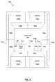
- FIG. 2illustrates the substrate layout 200 for the SERDES transceiver 100 according to embodiments of the present invention.
- the substrate layout 200is configured to minimize the substrate area of the transceiver 100 , and efficiently provide the port interconnections described above.
- the substrate layout 200is configured so that the parallel ports 102 a - 102 b and the serial ports 104 a - 104 d are on the outer perimeter of the substrate layout 200 , as shown.
- a logic core 202is at the center of the substrate layout 200 , where the logic core 202 operates the bus 106 , serial ports 104 , and parallel 102 ports.
- the management interface 116 , the packet BERT 112 , and the optional logic blocks 114 a - 114 care adjacent to the logic core 202 as shown.
- the bus 106can be described as a “ring” structure (or donut “structure”) around the logic core 202 , and placed in between the logic core 202 and the parallel ports 102 and serial ports 104 that occupy the parameter of the substrate layout 200 . Furthermore, the ring structure of the bus 106 also provides efficient communication between the logic core 202 and the various ports 102 and 104 . Furthermore, the ring structure of the bus 106 also provides efficient communication between the management interface 116 , the packet BERT 112 , the optional logic blocks 114 , and the various ports 102 and 104 .
- the bus 106is illustrated as eight sections 106 a - 106 g for ease of illustration. Each section provides an interface to the respective ports 102 or 104 that are adjacent to the respective sections.
- FIG. 3represents one of the eight sections 106 a - 106 g of the bus 106 according to embodiments of the present invention.
- Each section of the bus 106can be represented as two paths 308 and 310 .
- Dataenters the bus 106 through a buffer 302 and proceeds to its destination along the path 308 and through the buffers 304 .
- Once on the bus 106data passes from one section to another section of the bus 106 using the path 310 and passing through the buffers 312 .
- the mux 306represents data passing from the bus 106 to a functional block, such as a parallel port 102 , serial port 104 , or packet BERT 112 .
- the actual wires and buffers on the bus 106are matched to minimize signal distortion.
- the data wires in the bus 106are deposited on the substrate for substrate layout 200 in a particular fashion. Namely, a power or ground is placed between adjacent (or near by) data wires. Furthermore, adjacent data wires on the bus 106 are placed on two separate layers. Therefore, a power or ground will be above or below a data wire, and adjacent to a data wire. Therefore, two nearby data wires will not be located directly adjacent to one another, but instead will be positioned diagonally to each other, thereby reducing cross-talk.
- FIG. 4further illustrates an example layout of the bus 106 .
- the wires 402 between parallel ports 102 and serial ports 104are configured to have the same path lengths.
- wires 402 a - dare deposited so as to have the same path length so as to reduce signal distortion.
- FIG. 5illustrates another embodiment of the bus 106 in the substrate layout 200 .
- FIG. 4depicted only four wires 402 a - 402 d for connecting one port ( 102 or 104 ) to an adjacent port ( 102 or 104 )
- FIG. 5depicts a plurality of wires 402 a - 402 n for connecting two adjacent ports ( 102 and 104 ).
- the total number of wires 402 a - 402 nis determined by the design of the chip 100 .
- multi-port SERDES transceiver 100is programmable to support different data protocols, including, but not limited to, the XGMII protocol, the Ten Bit Interface (TBI) protocol, the Reduced TBI (RTBI) protocol, and the like.
- Transceiver 100is also programmable to support different electrical specifications, including, but not limited to, the High Speed Transistor Logic (HSTL) electrical specification, the Solid State Track Link (SSTL) electrical specification, the Low Voltage Transistor—Transistor Logic (LVTTL) electrical specification, and the like.
- the present inventionincludes methodologies or techniques for sending control signals to configure the parallel ports 102 a - 102 b to support a designated data protocol. This can be explained with reference to FIG.
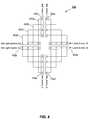
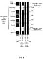
- Substrate layout 600includes a plurality of pads 604 a - 604 d that are part of the four serial ports 104 a - 104 d .
- each serial port 104includes a plurality of pads 604 .
- serial port 104 aincludes a plurality of pads 604 a .
- Serial port 104 bincludes a plurality of pads 604 b .
- Serial port 104 cincludes a plurality of pads 604 c .
- Serial port 104 dincludes a plurality of pads 604 d.
- Substrate layout 600also includes a plurality of pads 602 a - 602 d representing two parallel ports 102 a - 102 b .
- Pads 602 a - 602 bare part of parallel port 102 a
- pads 602 c - 602 dare part of parallel port 102 b .
- Pads 602 a and pads 602 dare input pads.
- transceiver 100receives data and control signals at input pads 602 a and input pads 602 d .
- Pads 602 b and 602 care output pads that enable transceiver 100 to transmit data and control signals.
- each group of pads 602includes forty-four individual pads.
- the padsForty of the pads are dedicated to sending or receiving data signals, and four of the pads are dedicated to sending or receiving control signals (e.g., clock signals).
- the total quantity of padscan be increased or decreased as determined by the system designer.
- the ratio of data-to-control padscan also be increased or decreased to meet system requirements as determined by the designer.
- Substrate layout 600also includes a plurality of management data input/output (MDIO) pads 606 a - 606 d .
- MDIO pads 606 a - 606 drepresent another embodiment of pads 117 a - 117 b , which are described above with reference to FIG. 1 .
- MDIO pads 606 a - 606 dare programmable to configure pads 602 a - 602 d and 604 a - 604 d for compliance with a designated electrical specification and/or data protocol.
- the electrical specification and/or data protocolis configured via an external pull-up or pull-down resistor(s) at the designated control pad.
- the electrical specificationsinclude IEEE 802.3TM clause 45, IEEE 802.3TM clause 22, or the like.
- MDIO pads 606 acontrol pads 602 a - 602 b
- MDIO pads 606 bcontrol pads 604 c - 604 d
- MDIO pads 606 ccontrol pads 602 c - 602 d
- MDIO pads 606 dcontrol pads 604 a - 604 b
- MDIO pads 606receive instructions from one or more management chips. These instructions are executed by the MDIO pads 606 to configure transceiver 100 and parallel ports 102 a - 102 b to be compatible with the designated electrical specification.
- one management chipis provided to instruct all MDIO pads 606 and their associated 10 pads 602 and/or 604 .
- a distinct management chipis provided to instruct each MDIO pad 606 and its associated 10 pads 602 and/or 604 .
- a separate management chipis provided to instruct a subset of MDIO pads 606 and their associated 10 pads 602 and/or 604 .
- serial IO pads 604 a - 604 d , parallel IO pads 602 a - 602 d , and MDIO pads 606 a - 606 dare positioned to provide rotational symmetry for substrate layout 600 . Therefore, if the transceiver 100 is rotated 180 degrees, the serial and parallel ports can be connected to another communications device without impeding the performance of transceiver 100 , or having to reconfigure either device.
- the symmetrical layout of the componentsalso allows efficiencies to be gained when the transceiver is being connected.
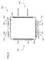
- FIG. 7illustrates a block diagram for logic or circuitry for a control system 700 for programming each pad 602 according to an embodiment of the present invention.
- Control system 700includes one or more programmable control registers 702 , a pad timing controller 704 , input controller 706 , output controller 708 , and configuration control logic 710 .
- Configuration control logic 710is responsive to various control signals, which are executed to program pad 602 such that it is capable of supporting a designated protocol.
- Input controller 706sends an input control signal 722 to configuration control logic 710 to program pad 602 to receive input.
- Output controller 708sends an output control signal 724 to configuration control logic 710 to program pad 602 to send output.
- Control registers 702includes five types of control signals for programming pad 602 .
- a system operatorinputs these control signals, but in an embodiment, the control signals are supplied by a computer system (not shown).
- the five control signalsinclude a reset message 712 , an Iddq message 714 , a power down message 716 , a pad type message 718 , and a delay select message 720 .
- a reset message 712is released to instruct pad 602 to change its originally designated function (i.e., input or output). For example, if pad 602 is originally designated as an output pad, the pad 602 is reconfigured to operate as an input pad upon receipt of a reset message 712 . In FIG. 7 , pad 602 is an output pad. Therefore, reset message 712 is only delivered to input controller 706 to enable pad 602 to switch to receiving input.
- Iddq message 714is released to implement Iddq testing to measure the quiescent supply current of transceiver 100 .
- Iddq message 714places the path across a pad 602 in a quiescent state to measure the leakage current.
- Iddq message 714is sent to input controller 706 , output controller 708 , and/or configuration control logic 710 for implementation.
- a power down message 714is released to suspend the operations of portions of pad 602 . If power down message 714 is delivered to input controller 706 , pad 602 no longer receives input. If power down message is delivered to output controller 708 , pad 602 no longer outputs data or control messages. If power down message 714 is delivered to configuration control logic 710 , the muxing and timing operations of the control logic 710 are suspended.
- PAD type message 718specifies the data protocol and electrical specification, and instructs configuration control logic 710 to implement the specified data protocol and electrical specification.
- the data protocolincludes the XGMII, TBI, RTBI protocols, and the like.
- the electrical specificationincludes HSTL, SSTL, and LVTTL electrical specifications, and the like.
- Delay select message 720specifies the path delay for input and output.
- the parameter specified in the delay select message 720enables the system operator, or the like, to adjust the delay between input and output at each pad 602 for better system performance.
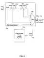
- flowchart 1000represents the general operational flow for configuring a programmable pad 602 to support a designated data protocol, according to an embodiment of the present invention.
- the control flow of flowchart 1000begins at step 1001 and passes immediately to step 1003 .
- protocol instructions for a designated data protocolare specified.
- the specified protocol instructionsare placed in programmable control registers 702 .
- a control signal carrying the protocol instructionsare released to program a pad 602 .
- the control signalis shown as PAD type message 718 , which is received by configuration control logic 710 .
- control signali.e., PAD type message 718
- PAD type message 718is executed to implement the specified data protocol.
- an output control signal 724 or input control signal 722is sent to configuration control logic 710 to instruct the programmable pad 602 to function as an output or input.
- pad 602transmits or receives in accordance with the specified data protocol. Afterwards, the control flow ends as indicated at step 1095 .
- pad 602is programmed to function as an output. However, pad 602 can be reconfigured to function as an input.
- flowchart 1100provides an example of a general operational flow for reconfiguring an output programmable pad 602 to function as an input.
- step 1101The control flow of flowchart 1100 begins at step 1101 and passes immediately to step 1103 .
- pad 602is instructed to cease functioning as an output.
- power down message 716is sent to output controller 708 , which as a result, stops sending output control signal 724 .
- step 1106input operations are initiated at pad 602 .
- reset message 712is sent to input controller 706 to initiate the operations.
- input control signal 722is sent to configuration control logic 710 .
- configuration control logic 710executes the input control signal 722 to configure pad 602 to start receiving input. Afterwards, the control flow ends as indicated at step 1195 .
- flowchart 1200provides an example of a general operational flow for programming pad 602 to perform Iddq testing.
- the control flow of flowchart 1200begins at step 1201 and passes immediately to step 1203 .
- Iddq message 714is released to either input controller 706 or output controller 708 , depending on the I/O operations currently designated for pad 602 .
- Iddq message 714is also released to configuration control logic 710 , which programs pad 602 to measure leakage as previously discussed. Afterwards, the control flow ends as indicated at step 1295 .
- pad timing controller 704receives pad data 726 from pad 602 .
- the delay select message 720instructs pad timing controller 704 to buffer the pad data 726 for a prescribed time period before sending the data to its destination as internal data 728 .
- the prescribed time periodis substantially the same as the path delay at other pads 602 .
- pad timing controller 704receives internal data 728 and buffers the data for a prescribed time period before enabling it to be output as pad data 726 .
- FIG. 8represents the buffering process for implementing path delay according to an embodiment of the present invention.
- pad timing controller 704includes a plurality of buffers 802 a - 802 n and a multiplexer 804 .
- Dataenters pad timing controller 704 and is delayed in one or more buffers 802 a - 802 n for a prescribed time period.
- the incoming datacan be pad data 726 received by pad 602 , or internal data 728 received from another portion of transceiver 100 .
- Each buffer 802 a - 802 ndelays the incoming data a fixed delay time.
- the delay timeis fixed internally. In other words, the system designer specifies the delay time for the buffers during fabrication of transceiver 100 , and this value is not changed by the control registers 702 or a system operator.
- the datais sent to the next buffer 802 a - 802 n unless multiplexer 804 opens the communications path to receive the data.
- the delay select message 720determines when multiplexer 804 opens the communications path.
- the communications pathcan be opened prior to the data entering one of the buffers 802 a - 802 n , or at any point after the data is released from one of the buffers 802 a - 802 n .
- the delay select message 720enables the path delay to be increased or decreased by specifying the number of buffers 802 a - 802 n , if any, that the data should traverse. Once the data is received by multiplexer 804 , the data is sent to its destination as pad data 726 or internal data 728 .
- the multi-port SERDES transceiver 100includes the ability to change the timing of parallel ports 102 and serial ports 104 . This includes the ability to change the timing between the data and clock signals.
- the registers in the parallel ports 102 and serial ports 104can be re-programmed to operate at different timing protocols.
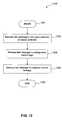
- flowchart 1300provides an example of a general operational flow for changing the timing protocol for a pad 602 .
- the control flow of flowchart 1300begins at step 1301 and passes immediately to step 1303 .
- one or more parametersare input to adjust the path delay.
- the parametersare entered at programmable control registers 702 .
- the delay parametersare communicated to PAD timing controller 704 .
- the delay parametersare encoded in delay select message 720 .
- the delay parametersare executed to specify the total delay period for the path delay.
- the total delay periodis measured by the quantity of buffers 802 a - 802 n that data must traverse before being received by multiplexer 804 .
- step 1312data (i.e., PAD data 726 or internal data 728 ) is received, and at step 1315 , the data is delayed the specified total delay period.
- step 1318the data is sent to its destination. Afterwards, the control flow ends as indicated at step 1395 .
- each MDIO pad 606 a - 606 dis programmable to configure itself to comply with a designated electrical standard, such as IEEE 802.3TM clause 22, IEEE 802.3TM clause 45, or the like.
- IEEE 802.3TM clause 22specifies the access to management scheme, including data protocol and electrical requirements.
- Pads 602 a - 602 dare programmable to support any combination of data protocols (e.g., XGMII, TBI, RTBI, etc.) and electrical specifications (e.g., HSTL, SSTL, LVTTL, etc.), and the electrical requirements are determined by the designated electrical specification.
- data protocolse.g., XGMII, TBI, RTBI, etc.
- electrical specificationse.g., HSTL, SSTL, LVTTL, etc.
- the electrical requirementsare determined by the designated electrical specification.
- the SSTL electrical specificationrequires pads 602 a - 602 d to operate at 2.5 volts.
- the HSTL electrical specificationrequires pads 602 a - 602 d to operate at 1.5 volts or 1.8 volts.
- the LVTTL electrical specificationrequires pads 602 a - 602 d to operate at 2.5 volts or 3.3 volts.
- MDIO pads 606 a - 606 dmust operate at 1.2 volts to comply with IEEE 802.3TM clause 45. To comply with IEEE 802.3TM clause 22, MDIO pads 606 a - 606 d must operate at 2.5 volts. Accordingly, MDIO pads 606 a - 606 d are programmable to configure themselves and their associated pads 602 a - 602 d to comply with the appropriate electrical requirements.
- a split-voltage bus structureis provided to connect the pads for transceiver 100 to a bus.
- An embodiment of a split-voltage bus structureis illustrated in FIG. 9 .
- FIG. 9illustrates power supply connections for MDIO pads 606 c - 606 d and output pads 602 c , according to an embodiment of the present invention.
- the power supply connectionsinclude VDDO I/O supply 912 , VSSO I/O supply 914 , VSSC core supply 916 , and VDDC core supply 918 .
- MDIO pads 606 c - 606 dare separated from output pads 602 c by split voltage structure 902 a - 902 b .
- Structure 902 a - 902 bbreaks the power bus VDDO I/O supply 912 , which allows different electrical requirements to be provided for MDIO pads 606 c - 606 d and the adjacent output pads 602 c .
- the power signals 904 , data signals 906 , clock signals 908 , and ground signals 910 for MDIO pads 606 c - 606 dwill not interfere with the electrical and data signals communicated from output pads 602 c .
- the connection for the VSSO I/O supply 914 , VSSC core supply 916 , and VDDC core supply 918is not broken by the structure 902 a - 902 b.
- flowchart 1400provides an example of a general operational flow for configuring a programmable pad (i.e., serial IO pads 604 a - 604 d , parallel IO pads 602 a - 602 d , and MDIO pads 606 a - 606 d ) to comply with a specified electrical standard, such as IEEE 802.3TM clause 22, IEEE 802.3TM clause 45, or the like.
- a programmable padi.e., serial IO pads 604 a - 604 d , parallel IO pads 602 a - 602 d , and MDIO pads 606 a - 606 d
- a specified electrical standardsuch as IEEE 802.3TM clause 22, IEEE 802.3TM clause 45, or the like.
- the control flow of flowchart 1400begins at step 1401 and passes immediately to step 1403 .
- MDIO instructionsare accessed to identify the specified electrical specification (e.g., HHTL, SSTL, LVTTL, etc.).
- the MDIO pad 606must operate at a certain voltage, depending on the specified electrical specification.
- the MDIO instructionsare executed to configure the electrical requirements for the associated 10 pads 602 and/or 604 .
- the IO pads 602 and/or 604may be required to operate at a different voltage than the MDIO pad 606 .
- step 1409data and control signals are sent or received at the MDIO pad 606 and IO pads 602 and/or 604 in accordance with the specified electrical specification. Afterwards, the control flow ends as indicated at step 1495 .
Landscapes
- Engineering & Computer Science (AREA)
- Theoretical Computer Science (AREA)
- General Engineering & Computer Science (AREA)
- Computer Networks & Wireless Communication (AREA)
- General Physics & Mathematics (AREA)
- Physics & Mathematics (AREA)
- Computer Hardware Design (AREA)
- Signal Processing (AREA)
- Information Transfer Systems (AREA)
- Semiconductor Integrated Circuits (AREA)
- Bus Control (AREA)
- Tests Of Electronic Circuits (AREA)
- Multi Processors (AREA)
Abstract
Description
Claims (20)
Priority Applications (2)
| Application Number | Priority Date | Filing Date | Title |
|---|---|---|---|
| US12/416,641US8086762B2 (en) | 2002-10-29 | 2009-04-01 | Programmable management IO pads for an integrated circuit |
| US13/305,207US20120072615A1 (en) | 2002-10-29 | 2011-11-28 | Programmable Management IO Pads for an Integrated Circuit |
Applications Claiming Priority (3)
| Application Number | Priority Date | Filing Date | Title |
|---|---|---|---|
| US42178002P | 2002-10-29 | 2002-10-29 | |
| US10/694,730US7533311B2 (en) | 2002-10-29 | 2003-10-29 | Programmable management IO pads for an integrated circuit |
| US12/416,641US8086762B2 (en) | 2002-10-29 | 2009-04-01 | Programmable management IO pads for an integrated circuit |
Related Parent Applications (1)
| Application Number | Title | Priority Date | Filing Date |
|---|---|---|---|
| US10/694,730DivisionUS7533311B2 (en) | 2002-10-29 | 2003-10-29 | Programmable management IO pads for an integrated circuit |
Related Child Applications (1)
| Application Number | Title | Priority Date | Filing Date |
|---|---|---|---|
| US13/305,207DivisionUS20120072615A1 (en) | 2002-10-29 | 2011-11-28 | Programmable Management IO Pads for an Integrated Circuit |
Publications (2)
| Publication Number | Publication Date |
|---|---|
| US20090252160A1 US20090252160A1 (en) | 2009-10-08 |
| US8086762B2true US8086762B2 (en) | 2011-12-27 |
Family
ID=32230269
Family Applications (13)
| Application Number | Title | Priority Date | Filing Date |
|---|---|---|---|
| US10/681,244Expired - LifetimeUS7373561B2 (en) | 2002-10-29 | 2003-10-09 | Integrated packet bit error rate tester for 10G SERDES |
| US10/694,788Expired - LifetimeUS7035228B2 (en) | 2002-10-29 | 2003-10-29 | Multi-rate, multi-port, gigabit Serdes transceiver |
| US10/694,729Expired - Fee RelatedUS7664888B2 (en) | 2002-10-29 | 2003-10-29 | Multipurpose and programmable pad ring for an integrated circuit |
| US10/695,498Expired - Fee RelatedUS7450530B2 (en) | 2002-10-29 | 2003-10-29 | Cross link multiplexer bus configured to reduce cross-talk |
| US10/695,458Expired - Fee RelatedUS7450529B2 (en) | 2002-10-29 | 2003-10-29 | Cross link multiplexer bus |
| US10/694,730Active2026-11-07US7533311B2 (en) | 2002-10-29 | 2003-10-29 | Programmable management IO pads for an integrated circuit |
| US11/389,506Expired - LifetimeUS7355987B2 (en) | 2002-10-29 | 2006-03-27 | Multi-rate, multi-port, gigabit SERDES transceiver |
| US12/078,780Expired - Fee RelatedUS8023436B2 (en) | 2002-10-29 | 2008-04-04 | Multi-rate, multi-port, gigabit serdes transceiver |
| US12/253,851Expired - Fee RelatedUS8094590B2 (en) | 2002-10-29 | 2008-10-17 | Cross link multiplexer bus |
| US12/416,641Expired - Fee RelatedUS8086762B2 (en) | 2002-10-29 | 2009-04-01 | Programmable management IO pads for an integrated circuit |
| US12/654,345Expired - Fee RelatedUS8001286B2 (en) | 2002-10-29 | 2009-12-17 | Multipurpose and programmable pad for an integrated circuit |
| US13/229,150Active2026-05-13US9330043B2 (en) | 2002-10-29 | 2011-09-09 | Multi-rate, multi-port, gigabit SERDES transceiver |
| US13/305,207AbandonedUS20120072615A1 (en) | 2002-10-29 | 2011-11-28 | Programmable Management IO Pads for an Integrated Circuit |
Family Applications Before (9)
| Application Number | Title | Priority Date | Filing Date |
|---|---|---|---|
| US10/681,244Expired - LifetimeUS7373561B2 (en) | 2002-10-29 | 2003-10-09 | Integrated packet bit error rate tester for 10G SERDES |
| US10/694,788Expired - LifetimeUS7035228B2 (en) | 2002-10-29 | 2003-10-29 | Multi-rate, multi-port, gigabit Serdes transceiver |
| US10/694,729Expired - Fee RelatedUS7664888B2 (en) | 2002-10-29 | 2003-10-29 | Multipurpose and programmable pad ring for an integrated circuit |
| US10/695,498Expired - Fee RelatedUS7450530B2 (en) | 2002-10-29 | 2003-10-29 | Cross link multiplexer bus configured to reduce cross-talk |
| US10/695,458Expired - Fee RelatedUS7450529B2 (en) | 2002-10-29 | 2003-10-29 | Cross link multiplexer bus |
| US10/694,730Active2026-11-07US7533311B2 (en) | 2002-10-29 | 2003-10-29 | Programmable management IO pads for an integrated circuit |
| US11/389,506Expired - LifetimeUS7355987B2 (en) | 2002-10-29 | 2006-03-27 | Multi-rate, multi-port, gigabit SERDES transceiver |
| US12/078,780Expired - Fee RelatedUS8023436B2 (en) | 2002-10-29 | 2008-04-04 | Multi-rate, multi-port, gigabit serdes transceiver |
| US12/253,851Expired - Fee RelatedUS8094590B2 (en) | 2002-10-29 | 2008-10-17 | Cross link multiplexer bus |
Family Applications After (3)
| Application Number | Title | Priority Date | Filing Date |
|---|---|---|---|
| US12/654,345Expired - Fee RelatedUS8001286B2 (en) | 2002-10-29 | 2009-12-17 | Multipurpose and programmable pad for an integrated circuit |
| US13/229,150Active2026-05-13US9330043B2 (en) | 2002-10-29 | 2011-09-09 | Multi-rate, multi-port, gigabit SERDES transceiver |
| US13/305,207AbandonedUS20120072615A1 (en) | 2002-10-29 | 2011-11-28 | Programmable Management IO Pads for an Integrated Circuit |
Country Status (3)
| Country | Link |
|---|---|
| US (13) | US7373561B2 (en) |
| EP (2) | EP2592529A1 (en) |
| WO (1) | WO2004040824A2 (en) |
Cited By (1)
| Publication number | Priority date | Publication date | Assignee | Title |
|---|---|---|---|---|
| US9632139B2 (en) | 2013-06-08 | 2017-04-25 | Silicon Mobility | IO pad circuitry with safety monitoring and control for integrated circuits |
Families Citing this family (93)
| Publication number | Priority date | Publication date | Assignee | Title |
|---|---|---|---|---|
| US6642136B1 (en)* | 2001-09-17 | 2003-11-04 | Megic Corporation | Method of making a low fabrication cost, high performance, high reliability chip scale package |
| US7099293B2 (en)* | 2002-05-01 | 2006-08-29 | Stmicroelectronics, Inc. | Buffer-less de-skewing for symbol combination in a CDMA demodulator |
| US7373561B2 (en)* | 2002-10-29 | 2008-05-13 | Broadcom Corporation | Integrated packet bit error rate tester for 10G SERDES |
| US8385188B2 (en)* | 2002-10-29 | 2013-02-26 | Broadcom Corporation | Multi-port, gigabit serdes transceiver capable of automatic fail switchover |
| US7525983B2 (en)* | 2003-07-21 | 2009-04-28 | Qlogic, Corporation | Method and system for selecting virtual lanes in fibre channel switches |
| US7684401B2 (en) | 2003-07-21 | 2010-03-23 | Qlogic, Corporation | Method and system for using extended fabric features with fibre channel switch elements |
| US7630384B2 (en)* | 2003-07-21 | 2009-12-08 | Qlogic, Corporation | Method and system for distributing credit in fibre channel systems |
| US7580354B2 (en)* | 2003-07-21 | 2009-08-25 | Qlogic, Corporation | Multi-speed cut through operation in fibre channel switches |
| US7558281B2 (en)* | 2003-07-21 | 2009-07-07 | Qlogic, Corporation | Method and system for configuring fibre channel ports |
| US7894348B2 (en) | 2003-07-21 | 2011-02-22 | Qlogic, Corporation | Method and system for congestion control in a fibre channel switch |
| US7430240B2 (en)* | 2003-10-29 | 2008-09-30 | Broadcom Corporation | Apparatus and method for automatic polarity swap in a communications system |
| US7606253B2 (en)* | 2004-01-12 | 2009-10-20 | Hewlett-Packard Development Company, L.P. | Successful transactions |
| US7672222B2 (en)* | 2004-01-12 | 2010-03-02 | Hewlett-Packard Development Company, L.P. | Link failures |
| US7613958B2 (en)* | 2004-01-12 | 2009-11-03 | Hewlett-Packard Development Company, L.P. | Error detection in a system having coupled channels |
| US7444454B2 (en)* | 2004-05-11 | 2008-10-28 | L-3 Communications Integrated Systems L.P. | Systems and methods for interconnection of multiple FPGA devices |
| US7921323B2 (en)* | 2004-05-11 | 2011-04-05 | L-3 Communications Integrated Systems, L.P. | Reconfigurable communications infrastructure for ASIC networks |
| US7461321B2 (en)* | 2004-05-25 | 2008-12-02 | Hewlett-Packard Development Company, L.P. | Error detection |
| US7624213B2 (en)* | 2005-02-11 | 2009-11-24 | Hewlett-Packard Development Company, L.P. | Passing identification information |
| US7721159B2 (en)* | 2005-02-11 | 2010-05-18 | Hewlett-Packard Development Company, L.P. | Passing debug information |
| US20050283669A1 (en)* | 2004-06-03 | 2005-12-22 | Adkisson Richard W | Edge detect circuit for performance counter |
| US7676530B2 (en)* | 2004-06-03 | 2010-03-09 | Hewlett-Packard Development Company, L.P. | Duration minimum and maximum circuit for performance counter |
| US7624319B2 (en)* | 2004-06-03 | 2009-11-24 | Hewlett-Packard Development Company, L.P. | Performance monitoring system |
| US8000322B2 (en)* | 2004-07-30 | 2011-08-16 | Hewlett-Packard Development Company, L.P. | Crossbar switch debugging |
| US7853837B2 (en)* | 2004-09-10 | 2010-12-14 | Rambus Inc. | Memory controller and method for operating a memory controller having an integrated bit error rate circuit |
| US7484027B1 (en)* | 2004-09-20 | 2009-01-27 | Cypress Semiconductor Corporation | Apparatus and method for configurable device pins |
| US8295299B2 (en) | 2004-10-01 | 2012-10-23 | Qlogic, Corporation | High speed fibre channel switch element |
| US7243182B2 (en)* | 2004-10-04 | 2007-07-10 | Cisco Technology, Inc. | Configurable high-speed serial links between components of a network device |
| US7386767B1 (en)* | 2004-10-05 | 2008-06-10 | Altera Corporation | Programmable bit error rate monitor for serial interface |
| US7346869B2 (en)* | 2004-10-29 | 2008-03-18 | Synopsys, Inc. | Power network analyzer for an integrated circuit design |
| US7536658B2 (en)* | 2004-10-29 | 2009-05-19 | Synopsys, Inc. | Power pad synthesizer for an integrated circuit design |
| US7353490B2 (en) | 2004-10-29 | 2008-04-01 | Synopsys, Inc. | Power network synthesizer for an integrated circuit design |
| US7656789B2 (en)* | 2005-03-29 | 2010-02-02 | International Business Machines Corporation | Method, system and storage medium for redundant input/output access |
| JP4649271B2 (en)* | 2005-06-08 | 2011-03-09 | キヤノン株式会社 | Control device |
| US7366817B2 (en)* | 2005-06-29 | 2008-04-29 | Intel Corporation | Frame order processing apparatus, systems, and methods |
| US7797463B2 (en)* | 2005-06-30 | 2010-09-14 | Intel Corporation | Hardware assisted receive channel frame handling via data offset comparison in SAS SSP wide port applications |
| US20070047589A1 (en)* | 2005-08-24 | 2007-03-01 | Bobak Modaress-Razavi | Multi-rate SERDES receiver |
| US7443760B2 (en)* | 2005-09-29 | 2008-10-28 | Hynix Semiconductor Inc. | Multi-port memory device with serial input/output interface |
| JP4641479B2 (en)* | 2005-09-29 | 2011-03-02 | キヤノン株式会社 | Image forming apparatus |
| US8441957B2 (en)* | 2005-10-17 | 2013-05-14 | Broadcom Corporation | Apparatus and method of remote PHY auto-negotiation |
| WO2007052090A1 (en)* | 2005-11-02 | 2007-05-10 | Freescale Semiconductor, Inc. | Device and a method for configuring input/output pads |
| US7974305B2 (en)* | 2006-03-24 | 2011-07-05 | Broadcom Corporation | Inband management for power over ethernet midspans using an embedded switch |
| US7955255B2 (en) | 2006-04-20 | 2011-06-07 | Boston Scientific Scimed, Inc. | Imaging assembly with transparent distal cap |
| TWI332771B (en) | 2006-09-04 | 2010-11-01 | Via Tech Inc | Receiver and test method therefor |
| US7808995B2 (en)* | 2006-11-16 | 2010-10-05 | L-3 Communications Integrated Systems L.P. | Methods and systems for relaying data packets |
| JP4465417B2 (en)* | 2006-12-14 | 2010-05-19 | インターナショナル・ビジネス・マシーンズ・コーポレーション | Customer segment estimation device |
| US8699514B2 (en) | 2007-01-12 | 2014-04-15 | Broadcom Corporation | Multi-rate MAC to PHY interface |
| KR100881670B1 (en)* | 2007-02-02 | 2009-02-06 | 삼성전자주식회사 | Apparatus and method for controlling analog block of data receiving device |
| US20080310315A1 (en)* | 2007-06-18 | 2008-12-18 | Lecroy Corporation | Equalized trigger |
| US8122297B2 (en)* | 2007-10-18 | 2012-02-21 | International Business Machines Corporation | Method and apparatus for parallel and serial data transfer |
| US7900098B2 (en)* | 2008-04-01 | 2011-03-01 | Intel Corporation | Receiver for recovering and retiming electromagnetically coupled data |
| US8391300B1 (en) | 2008-08-12 | 2013-03-05 | Qlogic, Corporation | Configurable switch element and methods thereof |
| US8793541B2 (en)* | 2008-10-10 | 2014-07-29 | Teledyne Lecroy, Inc. | Link equalization tester |
| US8347153B2 (en)* | 2008-10-10 | 2013-01-01 | Teledyne Lecroy, Inc. | Protocol aware error ratio tester |
| US8332552B2 (en)* | 2008-11-13 | 2012-12-11 | International Business Machines Corporation | Supporting multiple high bandwidth I/O controllers on a single chip |
| US8397054B2 (en)* | 2009-12-23 | 2013-03-12 | L-3 Communications Integrated Systems L.P. | Multi-phased computational reconfiguration |
| US8368423B2 (en)* | 2009-12-23 | 2013-02-05 | L-3 Communications Integrated Systems, L.P. | Heterogeneous computer architecture based on partial reconfiguration |
| US20110179315A1 (en)* | 2010-01-21 | 2011-07-21 | Brocade Communications Systems, Inc. | Serdes link error management |
| US8667343B2 (en) | 2010-03-11 | 2014-03-04 | The Johns Hopkins University | High speed error detector for fading propagation channels |
| US8543876B1 (en)* | 2010-06-18 | 2013-09-24 | Altera Corporation | Method and apparatus for serial scan test data delivery |
| US8433958B2 (en)* | 2010-09-17 | 2013-04-30 | Altera Corporation | Bit error rate checker receiving serial data signal from an eye viewer |
| US9222972B1 (en) | 2010-09-17 | 2015-12-29 | Altera Corporation | On-die jitter generator |
| US9106329B2 (en)* | 2011-01-31 | 2015-08-11 | Mediatek Inc. | Apparatus for communicating another device |
| US9253062B2 (en)* | 2011-12-23 | 2016-02-02 | Ixia | Byte by byte received data integrity check |
| US9148345B2 (en) | 2012-01-16 | 2015-09-29 | Ciena Corporation | Link management systems and methods for multi-stage, high-speed systems |
| US8995263B2 (en)* | 2012-05-22 | 2015-03-31 | Marvell World Trade Ltd. | Method and apparatus for internal/external memory packet and byte counting |
| US8762753B2 (en)* | 2012-06-17 | 2014-06-24 | Freescale Semiconductor, Inc. | Power management circuit using two configuration signals to control the power modes of two circuit modules using two crosslinked multiplexers and a level shifter |
| US9772651B2 (en)* | 2012-09-14 | 2017-09-26 | Samsung Electronics Co., Ltd. | Embedded multimedia card (eMMC), host controlling eMMC, and method operating eMMC system including the use of a switch command defining an adjustment delay for a data signal |
| US9471484B2 (en) | 2012-09-19 | 2016-10-18 | Novachips Canada Inc. | Flash memory controller having dual mode pin-out |
| US20140122777A1 (en)* | 2012-10-31 | 2014-05-01 | Mosaid Technologies Incorporated | Flash memory controller having multi mode pin-out |
| US9413651B2 (en) | 2012-12-14 | 2016-08-09 | Broadcom Corporation | Selective deep packet inspection |
| CN103487727B (en)* | 2013-06-21 | 2015-10-28 | 深圳供电局有限公司 | High-voltage power cable outer sheath fault online positioning method |
| US10382845B2 (en) | 2014-09-29 | 2019-08-13 | Fiber Mountain, Inc. | System for increasing fiber port density in data center applications |
| US9559834B1 (en) | 2015-01-26 | 2017-01-31 | Altera Corporation | Multi-rate transceiver circuitry |
| US9874863B2 (en)* | 2015-08-24 | 2018-01-23 | Keysight Technologies, Inc. | Finite state machine-based trigger event detection employing interpolation |
| US10572416B1 (en) | 2016-03-28 | 2020-02-25 | Aquantia Corporation | Efficient signaling scheme for high-speed ultra short reach interfaces |
| US11088876B1 (en)* | 2016-03-28 | 2021-08-10 | Marvell Asia Pte, Ltd. | Multi-chip module with configurable multi-mode serial link interfaces |
| US10613998B2 (en)* | 2018-07-30 | 2020-04-07 | EMC IP Holding Company LLC | Multi-level time decay storage queue |
| CN108957237B (en)* | 2018-08-01 | 2020-12-01 | 歌尔光学科技有限公司 | A kind of abnormal line detection method, device, equipment and storage medium |
| US11855056B1 (en) | 2019-03-15 | 2023-12-26 | Eliyan Corporation | Low cost solution for 2.5D and 3D packaging using USR chiplets |
| KR102855683B1 (en) | 2020-09-09 | 2025-09-05 | 삼성전자주식회사 | Semiconductor memory device and method and system of testing the same |
| US11855043B1 (en) | 2021-05-06 | 2023-12-26 | Eliyan Corporation | Complex system-in-package architectures leveraging high-bandwidth long-reach die-to-die connectivity over package substrates |
| US12438095B1 (en) | 2021-05-06 | 2025-10-07 | Eliyan Corp. | Complex system-in-package architectures leveraging high-bandwidth long-reach die-to-die connectivity over package substrates |
| US12204794B1 (en) | 2021-05-18 | 2025-01-21 | Eliyan Corporation | Architecture for DRAM control optimization using simultaneous bidirectional memory interfaces |
| US11748289B2 (en)* | 2021-11-16 | 2023-09-05 | Xilinx, Inc. | Protocol aware bridge circuit for low latency communication among integrated circuits |
| US12190038B1 (en) | 2021-11-25 | 2025-01-07 | Eliyan Corporation | Multi-chip module (MCM) with multi-port unified memory |
| US11842986B1 (en) | 2021-11-25 | 2023-12-12 | Eliyan Corporation | Multi-chip module (MCM) with interface adapter circuitry |
| US11841815B1 (en) | 2021-12-31 | 2023-12-12 | Eliyan Corporation | Chiplet gearbox for low-cost multi-chip module applications |
| US12248419B1 (en) | 2022-05-26 | 2025-03-11 | Eliyan Corporation | Interface conversion circuitry for universal chiplet interconnect express (UCIe) |
| CN116112394A (en)* | 2022-12-15 | 2023-05-12 | 广东博力威科技股份有限公司 | Method and system for testing data transmission error rate of BMS circuit board |
| US12058874B1 (en) | 2022-12-27 | 2024-08-06 | Eliyan Corporation | Universal network-attached memory architecture |
| US12182040B1 (en) | 2023-06-05 | 2024-12-31 | Eliyan Corporation | Multi-chip module (MCM) with scalable high bandwidth memory |
| US12204482B1 (en) | 2023-10-09 | 2025-01-21 | Eliyan Corporation | Memory chiplet with efficient mapping of memory-centric interface to die-to-die (D2D) unit interface modules |
| US12248413B1 (en) | 2023-10-11 | 2025-03-11 | Eliyan Corporation | Universal memory interface utilizing die-to-die (D2D) interfaces between chiplets |
Citations (64)
| Publication number | Priority date | Publication date | Assignee | Title |
|---|---|---|---|---|
| US4627070A (en) | 1981-09-16 | 1986-12-02 | Fmc Corporation | Asynchronous data bus system |
| US4833605A (en) | 1984-08-16 | 1989-05-23 | Mitsubishi Denki Kabushiki Kaisha | Cascaded information processing module having operation unit, parallel port, and serial port for concurrent data transfer and data processing |
| US4833695A (en) | 1987-09-08 | 1989-05-23 | Tektronix, Inc. | Apparatus for skew compensating signals |
| US4967201A (en) | 1987-10-22 | 1990-10-30 | Westinghouse Electric Corp. | Multi-layer single substrate microwave transmit/receive module |
| US5329520A (en) | 1992-07-17 | 1994-07-12 | Alcatel Network Systems, Inc. | High-speed facility protection in a digital telecommunications system |
| US5510950A (en)* | 1994-10-05 | 1996-04-23 | Ford Motor Company | Method and circuit for controlling and monitoring a load |
| US5594908A (en) | 1989-12-27 | 1997-01-14 | Hyatt; Gilbert P. | Computer system having a serial keyboard, a serial display, and a dynamic memory with memory refresh |
| US5617547A (en) | 1991-03-29 | 1997-04-01 | International Business Machines Corporation | Switch network extension of bus architecture |
| US5660568A (en) | 1995-01-04 | 1997-08-26 | Simple Technology, Inc. | Communications card with integral transmission media line adaptor |
| US5666071A (en)* | 1995-12-01 | 1997-09-09 | Advanced Micro Devices, Inc. | Device and method for programming high impedance states upon select input/output pads |
| US5726991A (en) | 1993-06-07 | 1998-03-10 | At&T Global Information Solutions Company | Integral bit error rate test system for serial data communication links |
| US5793990A (en) | 1993-06-11 | 1998-08-11 | Vlsi Technology, Inc. | Multiplex address/data bus with multiplex system controller and method therefor |
| US5803757A (en) | 1997-01-29 | 1998-09-08 | Wang; Tsan-Chi | Auto-termination single jack BNC connector |
| US5933021A (en) | 1996-06-18 | 1999-08-03 | Sun Microsystems, Inc | Noise suppression method and circuits for sensitive circuits |
| US5954811A (en) | 1996-01-25 | 1999-09-21 | Analog Devices, Inc. | Digital signal processor architecture |
| US5999021A (en) | 1996-08-20 | 1999-12-07 | Samsung Electronics Co., Ltd. | Pad signal detecting circuit in a semiconductor device for detecting a reference voltage in a high-speed interface |
| US6081570A (en) | 1997-09-02 | 2000-06-27 | The United States Of America As Represented By The Administrator Of The National Aeronautics And Space Administration | Parallel integrated frame synchronizer chip |
| US6087851A (en) | 1997-04-30 | 2000-07-11 | Samsung Electronics, Co., Ltd. | Method and apparatus for configuring a semiconductor device for compatibility with multiple logic interfaces |
| US6137734A (en) | 1999-03-30 | 2000-10-24 | Lsi Logic Corporation | Computer memory interface having a memory controller that automatically adjusts the timing of memory interface signals |
| US6140956A (en) | 1997-06-25 | 2000-10-31 | Cellutrac, Inc. | Vehicle tracking and security system incorporating simultaneous voice and data communication |
| US6167026A (en) | 1998-05-01 | 2000-12-26 | Emulex Corporation | Programmable error control circuit |
| US6172524B1 (en) | 1998-06-29 | 2001-01-09 | Hyundai Electronics Industries Co., Ltd. | Data input buffer |
| US6175556B1 (en) | 1994-06-06 | 2001-01-16 | International Business Machines Corporation | Remote powered ethernet repeater |
| US6183307B1 (en) | 1997-11-17 | 2001-02-06 | Xircom, Inc. | PC cards with integrated I/O communication receptacles |
| US20010000161A1 (en) | 1997-11-17 | 2001-04-05 | Xircom, Inc. | Type III PCMCIA card with integrated receptacles for receiving standard communications plugs |
| US6215412B1 (en) | 1991-03-29 | 2001-04-10 | International Business Machines Corporation | All-node switch-an unclocked, unbuffered, asynchronous switching apparatus |
| US6259693B1 (en) | 1997-08-28 | 2001-07-10 | Ascend Communications, Inc. | Cell combination to utilize available switch bandwidth |
| US20010009553A1 (en) | 1999-12-10 | 2001-07-26 | Magnus Homann | Dual speed end station and system |
| US20010012288A1 (en) | 1999-07-14 | 2001-08-09 | Shaohua Yu | Data transmission apparatus and method for transmitting data between physical layer side device and network layer device |
| US20010015664A1 (en) | 2000-02-23 | 2001-08-23 | Fujitsu Limited | Delay time adjusting method of delaying a phase of an output signal until a phase difference between an input signal and the output signal becomes an integral number of periods other than zero |
| US20010017595A1 (en) | 1998-05-27 | 2001-08-30 | Richard Cliff | Programmable voltage regulator |
| US20010021953A1 (en) | 2000-01-14 | 2001-09-13 | Katsuya Nakashima | Data processing circuit |
| US6317804B1 (en) | 1998-11-30 | 2001-11-13 | Philips Semiconductors Inc. | Concurrent serial interconnect for integrating functional blocks in an integrated circuit device |
| US20010043603A1 (en) | 1999-07-27 | 2001-11-22 | Shaohua Yu | Interfacing apparatus and method for adapting Ethernet directly to physical channel |
| US6346827B1 (en) | 1998-09-09 | 2002-02-12 | Altera Corporation | Programmable logic device input/output circuit configurable as reference voltage input circuit |
| US20020019173A1 (en) | 2000-03-20 | 2002-02-14 | David Oliphant | Modular jack for type III PCMCIA cards |
| US20020054569A1 (en) | 2000-11-07 | 2002-05-09 | Casio Computer Co., Ltd. | Data communication terminal |
| US20020095649A1 (en)* | 1997-11-12 | 2002-07-18 | Quickturn Design Systems, Inc. | Optimized emulation and prototyping architecture |
| US6434157B1 (en) | 1998-10-06 | 2002-08-13 | Schneider Automation, Inc. | MODBUS plus ethernet bridge |
| US6438717B1 (en) | 1999-05-26 | 2002-08-20 | 3Com Corporation | High speed parallel bit error rate tester |
| US20020157030A1 (en) | 2001-04-19 | 2002-10-24 | International Business Machines Corporation | Power conservation in communication systems |
| US20020163924A1 (en) | 2001-05-02 | 2002-11-07 | Kim Jason Seung-Min | General purpose input/ output controller |
| US20020165924A1 (en) | 1996-11-15 | 2002-11-07 | Canon Kabushiki Kaisha | Remote maintenance and servicing of a network peripheral device over the world wide web |
| US6483849B1 (en) | 1998-04-17 | 2002-11-19 | Advanced Micro Devices, Inc. | Network transceiver having a LED interface operable in parallel and serial modes |
| US6496880B1 (en)* | 1999-08-26 | 2002-12-17 | Agere Systems Inc. | Shared I/O ports for multi-core designs |
| US20030009307A1 (en) | 2001-01-18 | 2003-01-09 | Mejia Robert G. | Digital data pattern detection methods and arrangements |
| US6516352B1 (en) | 1998-08-17 | 2003-02-04 | Intel Corporation | Network interface system and method for dynamically switching between different physical layer devices |
| US20030048781A1 (en) | 1999-12-02 | 2003-03-13 | Worldcom, Inc. | Method and system for implementing an improved universal packet switching capability in a data switch |
| US6577157B1 (en)* | 1997-11-14 | 2003-06-10 | Altera Corporation | Fully programmable I/O pin with memory |
| US20030120791A1 (en) | 2001-12-20 | 2003-06-26 | Weber David M. | Multi-thread, multi-speed, multi-mode interconnect protocol controller |
| US20030172332A1 (en) | 2002-03-08 | 2003-09-11 | Jeffrey R. Rearick | Systems and methods for facilitating testing of pad drivers of integrated circuits |
| US20030214974A1 (en) | 2002-05-16 | 2003-11-20 | Beverly Harlan T. | Bus conversion device, system and method |
| US20040068593A1 (en) | 2002-10-08 | 2004-04-08 | Lsi Logic Corporation | High speed OC-768 configurable link layer chip |
| US20040083077A1 (en) | 2002-10-29 | 2004-04-29 | Broadcom Corporation | Integrated packet bit error rate tester for 10G SERDES |
| US6760781B1 (en) | 2000-02-16 | 2004-07-06 | 3Com Corporation | Intelligent packet transmission engine |
| US6789144B1 (en) | 1999-05-27 | 2004-09-07 | Advanced Micro Devices, Inc. | Apparatus and method in a network interface device for determining data availability in a random access memory |
| US6859825B1 (en) | 1999-12-29 | 2005-02-22 | Advanced Micro Devices, Inc. | System and method enabling configuration of physical layer devices and corresponding link partners for communicating network data via a configuration source or auto-negotiation |
| US6880078B2 (en) | 2002-11-06 | 2005-04-12 | Spirent Communications | Xaui extender card |
| US6895528B2 (en) | 2000-08-07 | 2005-05-17 | Computer Network Technology Corporation | Method and apparatus for imparting fault tolerance in a switch or the like |
| US20050190690A1 (en) | 2002-10-29 | 2005-09-01 | Broadcom Corporation | Multi-port, gigabit serdes transceiver capable of automatic fail switchover |
| US7032139B1 (en) | 2002-03-18 | 2006-04-18 | Finisar Corporation | Bit error rate tester |
| US7080162B2 (en) | 1999-09-21 | 2006-07-18 | Intel Corporation | Reduced hardware network adapter and communication method |
| US7133416B1 (en) | 2002-03-05 | 2006-11-07 | Mcdata Corporation | Converting data signals in a multiple communication protocol system area network |
| US7221652B1 (en) | 2001-12-14 | 2007-05-22 | Applied Micro Circuits Corporation | System and method for tolerating data link faults in communications with a switch fabric |
Family Cites Families (23)
| Publication number | Priority date | Publication date | Assignee | Title |
|---|---|---|---|---|
| US722652A (en)* | 1902-11-28 | 1903-03-10 | John H Schmeding | Box-lid holder. |
| FR2050036A5 (en) | 1969-06-06 | 1971-03-26 | Licentia Gmbh | |
| US4821174A (en)* | 1984-03-20 | 1989-04-11 | Westinghouse Electric Corp. | Signal processing system including a bus control module |
| JPS6276840A (en)* | 1985-09-30 | 1987-04-08 | Hitachi Ltd | node device |
| US4822605A (en)* | 1986-02-18 | 1989-04-18 | Exovir, Inc. | Compositions and methods employing the same for the treatment of viral and cancerous skin lesions and the like |
| IT1205762B (en)* | 1987-03-20 | 1989-03-31 | Enea | CAVITY FOR LASER FIR (FAR INFRARED RADIATION) OPTICALLY PUMPED WITH BEARING TUBE |
| US5864554A (en)* | 1993-10-20 | 1999-01-26 | Lsi Logic Corporation | Multi-port network adapter |
| WO1995015630A1 (en)* | 1993-11-30 | 1995-06-08 | Integrated Network Corporation | Network interface unit remote test pattern generation |
| DE69516444T2 (en)* | 1994-03-11 | 2001-01-04 | Intravascular Research Ltd., London | Ultrasonic transducer arrangement and method for its production |
| US5555540A (en)* | 1995-02-17 | 1996-09-10 | Sun Microsystems, Inc. | ASIC bus structure |
| US5908468A (en)* | 1997-10-24 | 1999-06-01 | Advanced Micro Devices, Inc. | Data transfer network on a chip utilizing a multiple traffic circle topology |
| US6069876A (en)* | 1997-02-13 | 2000-05-30 | Nortel Networks Corporation | Performance monitoring of an ATM Network |
| US6108801A (en)* | 1998-08-11 | 2000-08-22 | Cisco Systems, Inc. | Using profiles to perform Bit Error Rate Testing |
| DE19961131A1 (en)* | 1999-12-17 | 2002-07-18 | Siemens Ag | Device and method for compensating data transit times |
| DE10023614A1 (en)* | 2000-05-15 | 2001-11-22 | Nexpress Solutions Llc | Device for the manual exchange of a roller of a duplicating device |
| US6721313B1 (en)* | 2000-08-01 | 2004-04-13 | International Business Machines Corporation | Switch fabric architecture using integrated serdes transceivers |
| US6483344B2 (en)* | 2001-01-31 | 2002-11-19 | Stmicroelectronics, Inc. | Interconnect circuitry for implementing logic functions in a field programmable gate array and method of operation |
| US6664801B1 (en)* | 2001-05-21 | 2003-12-16 | Lsi Logic Corporation | IDDQ test methodology based on the sensitivity of fault current to power supply variations |
| US7280549B2 (en)* | 2001-07-09 | 2007-10-09 | Micron Technology, Inc. | High speed ring/bus |
| US7068650B1 (en)* | 2001-09-06 | 2006-06-27 | Cisco Technology, Inc. | Apparatus and method for SerDes rate matching using symbol interleaving |
| US7136400B2 (en)* | 2002-06-21 | 2006-11-14 | International Business Machines Corporation | Method and apparatus for multiplexing multiple protocol handlers on a shared memory bus |
| US20050250984A1 (en)* | 2004-05-07 | 2005-11-10 | Usgi Medical Inc. | Multiple removable apparatus and methods for manipulating and securing tissue |
| US8375146B2 (en)* | 2004-08-09 | 2013-02-12 | SanDisk Technologies, Inc. | Ring bus structure and its use in flash memory systems |
- 2003
- 2003-10-09USUS10/681,244patent/US7373561B2/ennot_activeExpired - Lifetime
- 2003-10-29WOPCT/US2003/034234patent/WO2004040824A2/enactiveApplication Filing
- 2003-10-29USUS10/694,788patent/US7035228B2/ennot_activeExpired - Lifetime
- 2003-10-29EPEP13000556.4Apatent/EP2592529A1/ennot_activeWithdrawn
- 2003-10-29USUS10/694,729patent/US7664888B2/ennot_activeExpired - Fee Related
- 2003-10-29USUS10/695,498patent/US7450530B2/ennot_activeExpired - Fee Related
- 2003-10-29USUS10/695,458patent/US7450529B2/ennot_activeExpired - Fee Related
- 2003-10-29EPEP03779391.6Apatent/EP1558987B1/ennot_activeExpired - Lifetime
- 2003-10-29USUS10/694,730patent/US7533311B2/enactiveActive
- 2006
- 2006-03-27USUS11/389,506patent/US7355987B2/ennot_activeExpired - Lifetime
- 2008
- 2008-04-04USUS12/078,780patent/US8023436B2/ennot_activeExpired - Fee Related
- 2008-10-17USUS12/253,851patent/US8094590B2/ennot_activeExpired - Fee Related
- 2009
- 2009-04-01USUS12/416,641patent/US8086762B2/ennot_activeExpired - Fee Related
- 2009-12-17USUS12/654,345patent/US8001286B2/ennot_activeExpired - Fee Related
- 2011
- 2011-09-09USUS13/229,150patent/US9330043B2/enactiveActive
- 2011-11-28USUS13/305,207patent/US20120072615A1/ennot_activeAbandoned
Patent Citations (72)
| Publication number | Priority date | Publication date | Assignee | Title |
|---|---|---|---|---|
| US4627070A (en) | 1981-09-16 | 1986-12-02 | Fmc Corporation | Asynchronous data bus system |
| US4833605A (en) | 1984-08-16 | 1989-05-23 | Mitsubishi Denki Kabushiki Kaisha | Cascaded information processing module having operation unit, parallel port, and serial port for concurrent data transfer and data processing |
| US4833695A (en) | 1987-09-08 | 1989-05-23 | Tektronix, Inc. | Apparatus for skew compensating signals |
| US4967201A (en) | 1987-10-22 | 1990-10-30 | Westinghouse Electric Corp. | Multi-layer single substrate microwave transmit/receive module |
| US5594908A (en) | 1989-12-27 | 1997-01-14 | Hyatt; Gilbert P. | Computer system having a serial keyboard, a serial display, and a dynamic memory with memory refresh |
| US5617547A (en) | 1991-03-29 | 1997-04-01 | International Business Machines Corporation | Switch network extension of bus architecture |
| US6215412B1 (en) | 1991-03-29 | 2001-04-10 | International Business Machines Corporation | All-node switch-an unclocked, unbuffered, asynchronous switching apparatus |
| US5329520A (en) | 1992-07-17 | 1994-07-12 | Alcatel Network Systems, Inc. | High-speed facility protection in a digital telecommunications system |
| US5726991A (en) | 1993-06-07 | 1998-03-10 | At&T Global Information Solutions Company | Integral bit error rate test system for serial data communication links |
| US5793990A (en) | 1993-06-11 | 1998-08-11 | Vlsi Technology, Inc. | Multiplex address/data bus with multiplex system controller and method therefor |
| US6175556B1 (en) | 1994-06-06 | 2001-01-16 | International Business Machines Corporation | Remote powered ethernet repeater |
| US5510950A (en)* | 1994-10-05 | 1996-04-23 | Ford Motor Company | Method and circuit for controlling and monitoring a load |
| US5660568A (en) | 1995-01-04 | 1997-08-26 | Simple Technology, Inc. | Communications card with integral transmission media line adaptor |
| US5666071A (en)* | 1995-12-01 | 1997-09-09 | Advanced Micro Devices, Inc. | Device and method for programming high impedance states upon select input/output pads |
| US5954811A (en) | 1996-01-25 | 1999-09-21 | Analog Devices, Inc. | Digital signal processor architecture |
| US5933021A (en) | 1996-06-18 | 1999-08-03 | Sun Microsystems, Inc | Noise suppression method and circuits for sensitive circuits |
| US5999021A (en) | 1996-08-20 | 1999-12-07 | Samsung Electronics Co., Ltd. | Pad signal detecting circuit in a semiconductor device for detecting a reference voltage in a high-speed interface |
| US20020165924A1 (en) | 1996-11-15 | 2002-11-07 | Canon Kabushiki Kaisha | Remote maintenance and servicing of a network peripheral device over the world wide web |
| US5803757A (en) | 1997-01-29 | 1998-09-08 | Wang; Tsan-Chi | Auto-termination single jack BNC connector |
| US6087851A (en) | 1997-04-30 | 2000-07-11 | Samsung Electronics, Co., Ltd. | Method and apparatus for configuring a semiconductor device for compatibility with multiple logic interfaces |
| US6140956A (en) | 1997-06-25 | 2000-10-31 | Cellutrac, Inc. | Vehicle tracking and security system incorporating simultaneous voice and data communication |
| US6259693B1 (en) | 1997-08-28 | 2001-07-10 | Ascend Communications, Inc. | Cell combination to utilize available switch bandwidth |
| US6081570A (en) | 1997-09-02 | 2000-06-27 | The United States Of America As Represented By The Administrator Of The National Aeronautics And Space Administration | Parallel integrated frame synchronizer chip |
| US20020095649A1 (en)* | 1997-11-12 | 2002-07-18 | Quickturn Design Systems, Inc. | Optimized emulation and prototyping architecture |
| US6577157B1 (en)* | 1997-11-14 | 2003-06-10 | Altera Corporation | Fully programmable I/O pin with memory |
| US20010000161A1 (en) | 1997-11-17 | 2001-04-05 | Xircom, Inc. | Type III PCMCIA card with integrated receptacles for receiving standard communications plugs |
| US6183307B1 (en) | 1997-11-17 | 2001-02-06 | Xircom, Inc. | PC cards with integrated I/O communication receptacles |
| US6483849B1 (en) | 1998-04-17 | 2002-11-19 | Advanced Micro Devices, Inc. | Network transceiver having a LED interface operable in parallel and serial modes |
| US6167026A (en) | 1998-05-01 | 2000-12-26 | Emulex Corporation | Programmable error control circuit |
| US20010017595A1 (en) | 1998-05-27 | 2001-08-30 | Richard Cliff | Programmable voltage regulator |
| US6172524B1 (en) | 1998-06-29 | 2001-01-09 | Hyundai Electronics Industries Co., Ltd. | Data input buffer |
| US6516352B1 (en) | 1998-08-17 | 2003-02-04 | Intel Corporation | Network interface system and method for dynamically switching between different physical layer devices |
| US6346827B1 (en) | 1998-09-09 | 2002-02-12 | Altera Corporation | Programmable logic device input/output circuit configurable as reference voltage input circuit |
| US6434157B1 (en) | 1998-10-06 | 2002-08-13 | Schneider Automation, Inc. | MODBUS plus ethernet bridge |
| US6317804B1 (en) | 1998-11-30 | 2001-11-13 | Philips Semiconductors Inc. | Concurrent serial interconnect for integrating functional blocks in an integrated circuit device |
| US6137734A (en) | 1999-03-30 | 2000-10-24 | Lsi Logic Corporation | Computer memory interface having a memory controller that automatically adjusts the timing of memory interface signals |
| US6438717B1 (en) | 1999-05-26 | 2002-08-20 | 3Com Corporation | High speed parallel bit error rate tester |
| US6789144B1 (en) | 1999-05-27 | 2004-09-07 | Advanced Micro Devices, Inc. | Apparatus and method in a network interface device for determining data availability in a random access memory |
| US20010012288A1 (en) | 1999-07-14 | 2001-08-09 | Shaohua Yu | Data transmission apparatus and method for transmitting data between physical layer side device and network layer device |
| US20010043603A1 (en) | 1999-07-27 | 2001-11-22 | Shaohua Yu | Interfacing apparatus and method for adapting Ethernet directly to physical channel |
| US6496880B1 (en)* | 1999-08-26 | 2002-12-17 | Agere Systems Inc. | Shared I/O ports for multi-core designs |
| US7080162B2 (en) | 1999-09-21 | 2006-07-18 | Intel Corporation | Reduced hardware network adapter and communication method |
| US20030048781A1 (en) | 1999-12-02 | 2003-03-13 | Worldcom, Inc. | Method and system for implementing an improved universal packet switching capability in a data switch |
| US20010009553A1 (en) | 1999-12-10 | 2001-07-26 | Magnus Homann | Dual speed end station and system |
| US6859825B1 (en) | 1999-12-29 | 2005-02-22 | Advanced Micro Devices, Inc. | System and method enabling configuration of physical layer devices and corresponding link partners for communicating network data via a configuration source or auto-negotiation |
| US20010021953A1 (en) | 2000-01-14 | 2001-09-13 | Katsuya Nakashima | Data processing circuit |
| US6760781B1 (en) | 2000-02-16 | 2004-07-06 | 3Com Corporation | Intelligent packet transmission engine |
| US20010015664A1 (en) | 2000-02-23 | 2001-08-23 | Fujitsu Limited | Delay time adjusting method of delaying a phase of an output signal until a phase difference between an input signal and the output signal becomes an integral number of periods other than zero |
| US20020019173A1 (en) | 2000-03-20 | 2002-02-14 | David Oliphant | Modular jack for type III PCMCIA cards |
| US6895528B2 (en) | 2000-08-07 | 2005-05-17 | Computer Network Technology Corporation | Method and apparatus for imparting fault tolerance in a switch or the like |
| US20020054569A1 (en) | 2000-11-07 | 2002-05-09 | Casio Computer Co., Ltd. | Data communication terminal |
| US20030009307A1 (en) | 2001-01-18 | 2003-01-09 | Mejia Robert G. | Digital data pattern detection methods and arrangements |
| US20020157030A1 (en) | 2001-04-19 | 2002-10-24 | International Business Machines Corporation | Power conservation in communication systems |
| US20020163924A1 (en) | 2001-05-02 | 2002-11-07 | Kim Jason Seung-Min | General purpose input/ output controller |
| US7221652B1 (en) | 2001-12-14 | 2007-05-22 | Applied Micro Circuits Corporation | System and method for tolerating data link faults in communications with a switch fabric |
| US20030120791A1 (en) | 2001-12-20 | 2003-06-26 | Weber David M. | Multi-thread, multi-speed, multi-mode interconnect protocol controller |
| US7133416B1 (en) | 2002-03-05 | 2006-11-07 | Mcdata Corporation | Converting data signals in a multiple communication protocol system area network |
| US20030172332A1 (en) | 2002-03-08 | 2003-09-11 | Jeffrey R. Rearick | Systems and methods for facilitating testing of pad drivers of integrated circuits |
| US7032139B1 (en) | 2002-03-18 | 2006-04-18 | Finisar Corporation | Bit error rate tester |
| US20030214974A1 (en) | 2002-05-16 | 2003-11-20 | Beverly Harlan T. | Bus conversion device, system and method |
| US20040068593A1 (en) | 2002-10-08 | 2004-04-08 | Lsi Logic Corporation | High speed OC-768 configurable link layer chip |
| US7035228B2 (en) | 2002-10-29 | 2006-04-25 | Broadcom Corporation | Multi-rate, multi-port, gigabit Serdes transceiver |
| US20040117698A1 (en) | 2002-10-29 | 2004-06-17 | Broadcom Corporation | Programmable management IO pads for an integrated circuit |
| US20050190690A1 (en) | 2002-10-29 | 2005-09-01 | Broadcom Corporation | Multi-port, gigabit serdes transceiver capable of automatic fail switchover |
| US20040088443A1 (en) | 2002-10-29 | 2004-05-06 | Broadcom Corporation | Multipurpose and programmable pad ring for an integrated circuit |
| US20040141497A1 (en) | 2002-10-29 | 2004-07-22 | Abbas Amirichimeh | Cross link multiplexer bus configured to reduce cross-talk |
| US20040083077A1 (en) | 2002-10-29 | 2004-04-29 | Broadcom Corporation | Integrated packet bit error rate tester for 10G SERDES |
| US20060250985A1 (en) | 2002-10-29 | 2006-11-09 | Broadcom Corporation | Multi-rate, multi-port, gigabit serdes transceiver |
| US20040141531A1 (en) | 2002-10-29 | 2004-07-22 | Abbas Amirichimeh | Cross link multiplexer bus |
| US7355987B2 (en) | 2002-10-29 | 2008-04-08 | Broadcom Corporation | Multi-rate, multi-port, gigabit SERDES transceiver |
| US7373561B2 (en) | 2002-10-29 | 2008-05-13 | Broadcom Corporation | Integrated packet bit error rate tester for 10G SERDES |
| US6880078B2 (en) | 2002-11-06 | 2005-04-12 | Spirent Communications | Xaui extender card |
Non-Patent Citations (37)
| Title |
|---|
| "4-Channel Multirate 1.0-3.2-GBPS Transceiver with High-Speed Redundancy" [online], BCM8021 Product Brief, Broadcom Corporation (2002) [retrieved on Jul. 16, 2003]. Retrieved from the Internet: (2 pages). |
| "4-Channel Multirate 1.0-3.2-GBPS Transceiver with High-Speed Redundancy" [online], BCM8021 Product Brief, Broadcom Corporation (2002) [retrieved on Jul. 16, 2003]. Retrieved from the Internet: <URL: http://www.broadcom.com/products/8021.html> (2 pages). |
| "8-Channel Multi-Rate CMOS Retimer with Full Redundancy" [online], BCM8040 Product Brief, Broadcom Corporation (2002) [retrieved on Jul. 16, 2003]. Retrieved from the Internet: (2 pages). |
| "8-Channel Multi-Rate CMOS Retimer with Full Redundancy" [online], BCM8040 Product Brief, Broadcom Corporation (2002) [retrieved on Jul. 16, 2003]. Retrieved from the Internet: <URL: http://www.broadcom.com/products/8040.html> (2 pages). |
| "8-Channel Multi-Rate CMOS Transceiver with Full Redundancy" [online], BCM8020 Product Brief, Broadcom Corporation (2002) [retrieved on Jul. 16, 2003]. Retrieved from the Internet: (2 pages). |
| "8-Channel Multi-Rate CMOS Transceiver with Full Redundancy" [online], BCM8020 Product Brief, Broadcom Corporation (2002) [retrieved on Jul. 16, 2003]. Retrieved from the Internet: <URL: http://www.broadcom.com/products/8020.html> (2 pages). |
| "BCM8020 8-Channel Multi-rate 1.0-3.2-GBPS Transceiver" [online], Broadcom Products Site Guide [retrieved on Jul. 16, 2003]. Retrieved from the Internet: (2 pages). |
| "BCM8020 8-Channel Multi-rate 1.0-3.2-GBPS Transceiver" [online], Broadcom Products Site Guide [retrieved on Jul. 16, 2003]. Retrieved from the Internet: <URL: http://www.broadcom.com/products/8020.html> (2 pages). |
| "BCM8021 4-Channel Multi-rate 1.0-3.2-GBPS Transceiver with High-Speed Redundancy" [online], Broadcom Products Site Guide [retrieved on Jul. 16, 2003]. Retrieved from the Internet: (2 pages). |
| "BCM8021 4-Channel Multi-rate 1.0-3.2-GBPS Transceiver with High-Speed Redundancy" [online], Broadcom Products Site Guide [retrieved on Jul. 16, 2003]. Retrieved from the Internet: <URL: http://www.broadcom.com/products/8021.html> (2 pages). |
| "BCM8040 8-Channel Multi-rate 1.0-3.2-GBPS Retimer Switch" [online], Broadcom Products Site Guide [retrieved on Jul. 16, 2003]. Retrieved from the Internet: (2 pages). |
| "BCM8040 8-Channel Multi-rate 1.0-3.2-GBPS Retimer Switch" [online], Broadcom Products Site Guide [retrieved on Jul. 16, 2003]. Retrieved from the Internet: <URL: http://www.broadcom.com/products/8040.html> (2 pages). |
| "Broadcom Announces the Industry's First 0.13-micron CMOS Advanced Transciver Solution with Signal Conditioning for Low-Cost 10-Gigabit Over Copper Links" [online], Broadcom Press Release, Apr. 29, 2003 [retrieved on Jul. 16, 2003]. Retrieved from the Internet: (4 pages). |
| "Broadcom Announces the Industry's First 0.13-micron CMOS Advanced Transciver Solution with Signal Conditioning for Low-Cost 10-Gigabit Over Copper Links" [online], Broadcom Press Release, Apr. 29, 2003 [retrieved on Jul. 16, 2003]. Retrieved from the Internet: <URL: http://www.broadcom.com/cgi-bin/pr/prps.cgi?pr—id=PR030429A> (4 pages). |
| "Broadcom Announces thr First 0.13-micron CMOS Multi-Rate Gigabit Octal Serializers/Deserializers"[online], Broadcom Press Release, Oct. 29, 2002 [retrieved on Jul. 16, 2003]. Retrieved from the Internet: (5 pages). |
| "Broadcom Announces thr First 0.13-micron CMOS Multi-Rate Gigabit Octal Serializers/Deserializers"[online], Broadcom Press Release, Oct. 29, 2002 [retrieved on Jul. 16, 2003]. Retrieved from the Internet: <URL: http://broadcom.com/cgi-bin/pr/prps.cgi?pr—id=PR021029> (5 pages). |
| Alaska Quad-Port Gigabit Ethernet Over Copper Transceivers, from http://www.marvell.com/products/transceivers/quadport/...., 1 page, printed May 8, 2007. |
| Alaska X10 Gigabit Ethernet Alaska Gigabit Ethernet Fast Ethernet Physical Layer (PHY) Transceiver Families Provide a Full Range of Ethernet Transceiver Solutions for the Broadband Communications Industry, from http://www.nuhorizons.com/FeaturedProducts/Volume3/Marvell/phy-transceiver.asp, 4 pages, Copyright 2007, printed May 8, 2007. |
| Cases et al., "Multiple Mode Selector for Input/Output Circuitry," Jul. 1, 1994, IP.com, pp. 1-3.* |
| Cisco Search: Results for "cdl" within "News@Cisco", from http://www.cisco.com/pcgi-bin/search/search.pl, Copyright 1992-2003, printed Jul. 29, 2003. |
| Cisco Systems, Cisco Systems ad Aretae Interactive Launch Internet Powered Property (IP2), http://newroom.cisco.com/dlls/global/asiapac/news/2000/pr-07-25.html. |
| Cisco Systems, Hiroshi Suzuki: Taking Ethernet Beyond the LAN, http://newsroom.cisco.com/dlls/innovators/optical/hiroshi-suzuki-profile.html. |
| Cisco Systems, Innovators Profiles, http://newsroom.cisco.com/dlls/innovators/inn-profiles.html. |
| Cisco Systems, Optical, http://newsroom.cisco.com/dlls/innovatros/optical/. |
| Cisco Systems, Q&A: Hiroshi Suzuki on Extending Ethernet Beyond the LAN, http://newsroom.cisco.com/dlls/innovators/optical/hiroshi-suzuki-qa.html. |
| David Maliniak (ed.), Bel's integrated connector modules support Marvell's Alaska quad Gigabit Ethernet transceiver, from http://www.electronicsweb.com/Content/news/...., 1 page, Dec. 14, 2000, printed May 8, 2007. |
| Ed Turner, David Law, Sep. 17-19, 2001, "IEEE P802.3ae MDC/MDIO", http://www.Ieee802.org/3/efm/public/sep01/turner.sub.-- 1.sub.--0901.pdf. |
| EtherLink III ISA Network Interface Card User Guide; Jan. 1998; pp. 1-110. |
| IEEE Std. 802.3, Part 3: Carrier Sense Multiple Access with Collision Detection (CSMA/CD) access method and physical layer specifications, Section Four, pp. 9-152, Copyright 2005. |
| IEEE Std. 802.3, Part 3: Carrier Sense Multiple Access with Collision Detection (CSMA/CD) access method and physical layer specifications, Section Two, pp. 9-55, Copyright 2002. |
| Industry Breakthrough: Marvell Announces the First Quad-Port Transceiver to Support Both Copper and Fiber-Optic Gigabit Ethernet Interfaces, from Business Wire at www.encyclopedia.com/printable/aspx?id=1G1:68912211, 4 pages, Jan. 9, 2001, printed May 8, 2007. |
| International Search Report Issued Dec. 14, 2004 for International Application No. PCT/US03/34234, 5 pages. |
| Marvell Gets Small, from http://www.lightreading.com/document.asp?doc-id=12004&print=true, 1 page, Feb. 19, 2002, printed May 8, 2007. |
| Marvell Introduces the Industry's Smallest Quad-Port Gigabit Transceiver Device, Enabling Ultra High Port Density Enterprise Switching Systems, from http://www.marvell.com/press/pressNewsDisplay.do?releaseID-41, 3 pages, Feb. 19, 2002, printed May 8, 2007. |
| McKenzie, Alan, "Multi-Function Input/Output Pad Interfaces Shared Between Programmable and Microprocessor Cores, Integrated Within a Programmable SOC Solution," Mar. 11, 2001, IP.com, pp. 1-4.* |
| Q&A: Hiroshi Suzuki on Extending Ethernet Beyond the LAN, from http://newsroom.cisco.com/dlls/innovators/optical/hiroshi-suzuki-qa.html, 3 pages, Copyright 1992-2003, printed Jul. 29, 2003. |
| The Institute of Electrical and Electronic Engineering, Inc. (IEEE); IEEE 100 The Authoritative Dictionary of IEEE standards terms, Dec. 2000; Standards Information Network IEEE Press; Seventh Edition; p. 1196. |
Cited By (1)
| Publication number | Priority date | Publication date | Assignee | Title |
|---|---|---|---|---|
| US9632139B2 (en) | 2013-06-08 | 2017-04-25 | Silicon Mobility | IO pad circuitry with safety monitoring and control for integrated circuits |
Also Published As
| Publication number | Publication date |
|---|---|
| US20090041060A1 (en) | 2009-02-12 |
| EP1558987A4 (en) | 2010-06-23 |
| WO2004040824A3 (en) | 2005-02-10 |
| US20060250985A1 (en) | 2006-11-09 |
| WO2004040824A2 (en) | 2004-05-13 |
| US8023436B2 (en) | 2011-09-20 |
| EP1558987A2 (en) | 2005-08-03 |
| US20040141531A1 (en) | 2004-07-22 |
| US8094590B2 (en) | 2012-01-10 |
| US9330043B2 (en) | 2016-05-03 |
| US20040141497A1 (en) | 2004-07-22 |
| US7664888B2 (en) | 2010-02-16 |
| US20090252160A1 (en) | 2009-10-08 |
| US7035228B2 (en) | 2006-04-25 |
| US20100100651A1 (en) | 2010-04-22 |
| US8001286B2 (en) | 2011-08-16 |
| US20040083077A1 (en) | 2004-04-29 |
| US7373561B2 (en) | 2008-05-13 |
| EP1558987B1 (en) | 2013-09-11 |
| US7450530B2 (en) | 2008-11-11 |
| US7450529B2 (en) | 2008-11-11 |
| US20120072615A1 (en) | 2012-03-22 |
| US7355987B2 (en) | 2008-04-08 |
| US7533311B2 (en) | 2009-05-12 |
| US20040088444A1 (en) | 2004-05-06 |
| EP2592529A1 (en) | 2013-05-15 |
| US20040117698A1 (en) | 2004-06-17 |
| US20120239846A1 (en) | 2012-09-20 |
| US20040088443A1 (en) | 2004-05-06 |
| US20080186987A1 (en) | 2008-08-07 |
Similar Documents
| Publication | Publication Date | Title |
|---|---|---|
| US8086762B2 (en) | Programmable management IO pads for an integrated circuit | |
| US7630446B2 (en) | Apparatus and method for automatic polarity swap in a communications system | |
| US7557605B2 (en) | Heterogeneous configurable integrated circuit | |
| US8046510B2 (en) | Physical layer device having a SERDES pass through mode | |
| US8711677B2 (en) | Multi-port, gigabit SERDES transceiver capable of automatic fail switchover | |
| US8488623B2 (en) | Scalable interconnect modules with flexible channel bonding | |
| EP1219031B1 (en) | Integrated circuit including dedicated and programmable logic | |
| US6275975B1 (en) | Scalable mesh architecture with reconfigurable paths for an on-chip data transfer network incorporating a network configuration manager | |
| KR100686182B1 (en) | IP core scan test control device in network on chip | |
| US20020191601A1 (en) | On-chip communication architecture and method | |
| EP4572146A1 (en) | Techniques for configuring repeater circuits in active interconnection devices | |
| CN118567924A (en) | A DRP-based FPGA embedded Interlaken IP testing method and system | |
| JPH11127074A (en) | Field programmable gate array |
Legal Events
| Date | Code | Title | Description |
|---|---|---|---|
| AS | Assignment | Owner name:BROADCOM CORPORATION, CALIFORNIA Free format text:ASSIGNMENT OF ASSIGNORS INTEREST;ASSIGNORS:TRAN, HOANG;BAUMER, HOWARD A.;REEL/FRAME:022625/0389;SIGNING DATES FROM 20031027 TO 20031028 Owner name:BROADCOM CORPORATION, CALIFORNIA Free format text:ASSIGNMENT OF ASSIGNORS INTEREST;ASSIGNORS:TRAN, HOANG;BAUMER, HOWARD A.;SIGNING DATES FROM 20031027 TO 20031028;REEL/FRAME:022625/0389 | |
| XAS | Not any more in us assignment database | Free format text:ASSIGNMENT OF ASSIGNORS INTEREST;ASSIGNORS:TRAN, HOANG;BAUMER, HOWARD A.;SIGNING DATES FROM 20031027 TO 20031028;REEL/FRAME:022489/0218 | |
| ZAAA | Notice of allowance and fees due | Free format text:ORIGINAL CODE: NOA | |
| ZAAB | Notice of allowance mailed | Free format text:ORIGINAL CODE: MN/=. | |
| STCF | Information on status: patent grant | Free format text:PATENTED CASE | |
| FPAY | Fee payment | Year of fee payment:4 | |
| AS | Assignment | Owner name:BANK OF AMERICA, N.A., AS COLLATERAL AGENT, NORTH CAROLINA Free format text:PATENT SECURITY AGREEMENT;ASSIGNOR:BROADCOM CORPORATION;REEL/FRAME:037806/0001 Effective date:20160201 Owner name:BANK OF AMERICA, N.A., AS COLLATERAL AGENT, NORTH Free format text:PATENT SECURITY AGREEMENT;ASSIGNOR:BROADCOM CORPORATION;REEL/FRAME:037806/0001 Effective date:20160201 | |
| AS | Assignment | Owner name:AVAGO TECHNOLOGIES GENERAL IP (SINGAPORE) PTE. LTD., SINGAPORE Free format text:ASSIGNMENT OF ASSIGNORS INTEREST;ASSIGNOR:BROADCOM CORPORATION;REEL/FRAME:041706/0001 Effective date:20170120 Owner name:AVAGO TECHNOLOGIES GENERAL IP (SINGAPORE) PTE. LTD Free format text:ASSIGNMENT OF ASSIGNORS INTEREST;ASSIGNOR:BROADCOM CORPORATION;REEL/FRAME:041706/0001 Effective date:20170120 | |
| AS | Assignment | Owner name:BROADCOM CORPORATION, CALIFORNIA Free format text:TERMINATION AND RELEASE OF SECURITY INTEREST IN PATENTS;ASSIGNOR:BANK OF AMERICA, N.A., AS COLLATERAL AGENT;REEL/FRAME:041712/0001 Effective date:20170119 | |
| AS | Assignment | Owner name:AVAGO TECHNOLOGIES INTERNATIONAL SALES PTE. LIMITE Free format text:MERGER;ASSIGNOR:AVAGO TECHNOLOGIES GENERAL IP (SINGAPORE) PTE. LTD.;REEL/FRAME:047196/0687 Effective date:20180509 | |
| AS | Assignment | Owner name:AVAGO TECHNOLOGIES INTERNATIONAL SALES PTE. LIMITE Free format text:CORRECTIVE ASSIGNMENT TO CORRECT THE EFFECTIVE DATE OF MERGER TO 9/5/2018 PREVIOUSLY RECORDED AT REEL: 047196 FRAME: 0687. ASSIGNOR(S) HEREBY CONFIRMS THE MERGER;ASSIGNOR:AVAGO TECHNOLOGIES GENERAL IP (SINGAPORE) PTE. LTD.;REEL/FRAME:047630/0344 Effective date:20180905 | |
| AS | Assignment | Owner name:AVAGO TECHNOLOGIES INTERNATIONAL SALES PTE. LIMITE Free format text:CORRECTIVE ASSIGNMENT TO CORRECT THE PROPERTY NUMBERS PREVIOUSLY RECORDED AT REEL: 47630 FRAME: 344. ASSIGNOR(S) HEREBY CONFIRMS THE ASSIGNMENT;ASSIGNOR:AVAGO TECHNOLOGIES GENERAL IP (SINGAPORE) PTE. LTD.;REEL/FRAME:048883/0267 Effective date:20180905 | |
| MAFP | Maintenance fee payment | Free format text:PAYMENT OF MAINTENANCE FEE, 8TH YEAR, LARGE ENTITY (ORIGINAL EVENT CODE: M1552); ENTITY STATUS OF PATENT OWNER: LARGE ENTITY Year of fee payment:8 | |
| FEPP | Fee payment procedure | Free format text:MAINTENANCE FEE REMINDER MAILED (ORIGINAL EVENT CODE: REM.); ENTITY STATUS OF PATENT OWNER: LARGE ENTITY | |
| LAPS | Lapse for failure to pay maintenance fees | Free format text:PATENT EXPIRED FOR FAILURE TO PAY MAINTENANCE FEES (ORIGINAL EVENT CODE: EXP.); ENTITY STATUS OF PATENT OWNER: LARGE ENTITY | |
| STCH | Information on status: patent discontinuation | Free format text:PATENT EXPIRED DUE TO NONPAYMENT OF MAINTENANCE FEES UNDER 37 CFR 1.362 | |
| FP | Lapsed due to failure to pay maintenance fee | Effective date:20231227 |