US8084866B2 - Microelectronic devices and methods for filling vias in microelectronic devices - Google Patents
Microelectronic devices and methods for filling vias in microelectronic devicesDownload PDFInfo
- Publication number
- US8084866B2 US8084866B2US10/733,226US73322603AUS8084866B2US 8084866 B2US8084866 B2US 8084866B2US 73322603 AUS73322603 AUS 73322603AUS 8084866 B2US8084866 B2US 8084866B2
- Authority
- US
- United States
- Prior art keywords
- conductive material
- die
- microelectronic device
- bond
- pad
- Prior art date
- Legal status (The legal status is an assumption and is not a legal conclusion. Google has not performed a legal analysis and makes no representation as to the accuracy of the status listed.)
- Active, expires
Links
Images


Classifications
- H—ELECTRICITY
- H01—ELECTRIC ELEMENTS
- H01L—SEMICONDUCTOR DEVICES NOT COVERED BY CLASS H10
- H01L21/00—Processes or apparatus adapted for the manufacture or treatment of semiconductor or solid state devices or of parts thereof
- H01L21/70—Manufacture or treatment of devices consisting of a plurality of solid state components formed in or on a common substrate or of parts thereof; Manufacture of integrated circuit devices or of parts thereof
- H01L21/71—Manufacture of specific parts of devices defined in group H01L21/70
- H01L21/768—Applying interconnections to be used for carrying current between separate components within a device comprising conductors and dielectrics
- H01L21/76898—Applying interconnections to be used for carrying current between separate components within a device comprising conductors and dielectrics formed through a semiconductor substrate
- H—ELECTRICITY
- H01—ELECTRIC ELEMENTS
- H01L—SEMICONDUCTOR DEVICES NOT COVERED BY CLASS H10
- H01L21/00—Processes or apparatus adapted for the manufacture or treatment of semiconductor or solid state devices or of parts thereof
- H01L21/67—Apparatus specially adapted for handling semiconductor or electric solid state devices during manufacture or treatment thereof; Apparatus specially adapted for handling wafers during manufacture or treatment of semiconductor or electric solid state devices or components ; Apparatus not specifically provided for elsewhere
- H01L21/683—Apparatus specially adapted for handling semiconductor or electric solid state devices during manufacture or treatment thereof; Apparatus specially adapted for handling wafers during manufacture or treatment of semiconductor or electric solid state devices or components ; Apparatus not specifically provided for elsewhere for supporting or gripping
- H01L21/6835—Apparatus specially adapted for handling semiconductor or electric solid state devices during manufacture or treatment thereof; Apparatus specially adapted for handling wafers during manufacture or treatment of semiconductor or electric solid state devices or components ; Apparatus not specifically provided for elsewhere for supporting or gripping using temporarily an auxiliary support
- H—ELECTRICITY
- H01—ELECTRIC ELEMENTS
- H01L—SEMICONDUCTOR DEVICES NOT COVERED BY CLASS H10
- H01L23/00—Details of semiconductor or other solid state devices
- H01L23/48—Arrangements for conducting electric current to or from the solid state body in operation, e.g. leads, terminal arrangements ; Selection of materials therefor
- H01L23/481—Internal lead connections, e.g. via connections, feedthrough structures
- H—ELECTRICITY
- H01—ELECTRIC ELEMENTS
- H01L—SEMICONDUCTOR DEVICES NOT COVERED BY CLASS H10
- H01L25/00—Assemblies consisting of a plurality of semiconductor or other solid state devices
- H01L25/03—Assemblies consisting of a plurality of semiconductor or other solid state devices all the devices being of a type provided for in a single subclass of subclasses H10B, H10D, H10F, H10H, H10K or H10N, e.g. assemblies of rectifier diodes
- H01L25/04—Assemblies consisting of a plurality of semiconductor or other solid state devices all the devices being of a type provided for in a single subclass of subclasses H10B, H10D, H10F, H10H, H10K or H10N, e.g. assemblies of rectifier diodes the devices not having separate containers
- H01L25/065—Assemblies consisting of a plurality of semiconductor or other solid state devices all the devices being of a type provided for in a single subclass of subclasses H10B, H10D, H10F, H10H, H10K or H10N, e.g. assemblies of rectifier diodes the devices not having separate containers the devices being of a type provided for in group H10D89/00
- H01L25/0657—Stacked arrangements of devices
- H—ELECTRICITY
- H01—ELECTRIC ELEMENTS
- H01L—SEMICONDUCTOR DEVICES NOT COVERED BY CLASS H10
- H01L25/00—Assemblies consisting of a plurality of semiconductor or other solid state devices
- H01L25/50—Multistep manufacturing processes of assemblies consisting of devices, the devices being individual devices of subclass H10D or integrated devices of class H10
- H—ELECTRICITY
- H01—ELECTRIC ELEMENTS
- H01L—SEMICONDUCTOR DEVICES NOT COVERED BY CLASS H10
- H01L2224/00—Indexing scheme for arrangements for connecting or disconnecting semiconductor or solid-state bodies and methods related thereto as covered by H01L24/00
- H01L2224/01—Means for bonding being attached to, or being formed on, the surface to be connected, e.g. chip-to-package, die-attach, "first-level" interconnects; Manufacturing methods related thereto
- H01L2224/26—Layer connectors, e.g. plate connectors, solder or adhesive layers; Manufacturing methods related thereto
- H01L2224/31—Structure, shape, material or disposition of the layer connectors after the connecting process
- H01L2224/32—Structure, shape, material or disposition of the layer connectors after the connecting process of an individual layer connector
- H01L2224/321—Disposition
- H01L2224/32135—Disposition the layer connector connecting between different semiconductor or solid-state bodies, i.e. chip-to-chip
- H01L2224/32145—Disposition the layer connector connecting between different semiconductor or solid-state bodies, i.e. chip-to-chip the bodies being stacked
- H—ELECTRICITY
- H01—ELECTRIC ELEMENTS
- H01L—SEMICONDUCTOR DEVICES NOT COVERED BY CLASS H10
- H01L2224/00—Indexing scheme for arrangements for connecting or disconnecting semiconductor or solid-state bodies and methods related thereto as covered by H01L24/00
- H01L2224/01—Means for bonding being attached to, or being formed on, the surface to be connected, e.g. chip-to-package, die-attach, "first-level" interconnects; Manufacturing methods related thereto
- H01L2224/42—Wire connectors; Manufacturing methods related thereto
- H01L2224/47—Structure, shape, material or disposition of the wire connectors after the connecting process
- H01L2224/48—Structure, shape, material or disposition of the wire connectors after the connecting process of an individual wire connector
- H01L2224/4805—Shape
- H01L2224/4809—Loop shape
- H01L2224/48091—Arched
- H—ELECTRICITY
- H01—ELECTRIC ELEMENTS
- H01L—SEMICONDUCTOR DEVICES NOT COVERED BY CLASS H10
- H01L2224/00—Indexing scheme for arrangements for connecting or disconnecting semiconductor or solid-state bodies and methods related thereto as covered by H01L24/00
- H01L2224/01—Means for bonding being attached to, or being formed on, the surface to be connected, e.g. chip-to-package, die-attach, "first-level" interconnects; Manufacturing methods related thereto
- H01L2224/42—Wire connectors; Manufacturing methods related thereto
- H01L2224/47—Structure, shape, material or disposition of the wire connectors after the connecting process
- H01L2224/48—Structure, shape, material or disposition of the wire connectors after the connecting process of an individual wire connector
- H01L2224/481—Disposition
- H01L2224/48135—Connecting between different semiconductor or solid-state bodies, i.e. chip-to-chip
- H01L2224/48145—Connecting between different semiconductor or solid-state bodies, i.e. chip-to-chip the bodies being stacked
- H—ELECTRICITY
- H01—ELECTRIC ELEMENTS
- H01L—SEMICONDUCTOR DEVICES NOT COVERED BY CLASS H10
- H01L2224/00—Indexing scheme for arrangements for connecting or disconnecting semiconductor or solid-state bodies and methods related thereto as covered by H01L24/00
- H01L2224/73—Means for bonding being of different types provided for in two or more of groups H01L2224/10, H01L2224/18, H01L2224/26, H01L2224/34, H01L2224/42, H01L2224/50, H01L2224/63, H01L2224/71
- H01L2224/732—Location after the connecting process
- H01L2224/73201—Location after the connecting process on the same surface
- H01L2224/73207—Bump and wire connectors
- H—ELECTRICITY
- H01—ELECTRIC ELEMENTS
- H01L—SEMICONDUCTOR DEVICES NOT COVERED BY CLASS H10
- H01L2224/00—Indexing scheme for arrangements for connecting or disconnecting semiconductor or solid-state bodies and methods related thereto as covered by H01L24/00
- H01L2224/73—Means for bonding being of different types provided for in two or more of groups H01L2224/10, H01L2224/18, H01L2224/26, H01L2224/34, H01L2224/42, H01L2224/50, H01L2224/63, H01L2224/71
- H01L2224/732—Location after the connecting process
- H01L2224/73251—Location after the connecting process on different surfaces
- H01L2224/73257—Bump and wire connectors
- H—ELECTRICITY
- H01—ELECTRIC ELEMENTS
- H01L—SEMICONDUCTOR DEVICES NOT COVERED BY CLASS H10
- H01L2225/00—Details relating to assemblies covered by the group H01L25/00 but not provided for in its subgroups
- H01L2225/03—All the devices being of a type provided for in the same main group of the same subclass of class H10, e.g. assemblies of rectifier diodes
- H01L2225/04—All the devices being of a type provided for in the same main group of the same subclass of class H10, e.g. assemblies of rectifier diodes the devices not having separate containers
- H01L2225/065—All the devices being of a type provided for in the same main group of the same subclass of class H10
- H01L2225/06503—Stacked arrangements of devices
- H01L2225/06506—Wire or wire-like electrical connections between devices
- H—ELECTRICITY
- H01—ELECTRIC ELEMENTS
- H01L—SEMICONDUCTOR DEVICES NOT COVERED BY CLASS H10
- H01L2225/00—Details relating to assemblies covered by the group H01L25/00 but not provided for in its subgroups
- H01L2225/03—All the devices being of a type provided for in the same main group of the same subclass of class H10, e.g. assemblies of rectifier diodes
- H01L2225/04—All the devices being of a type provided for in the same main group of the same subclass of class H10, e.g. assemblies of rectifier diodes the devices not having separate containers
- H01L2225/065—All the devices being of a type provided for in the same main group of the same subclass of class H10
- H01L2225/06503—Stacked arrangements of devices
- H01L2225/06513—Bump or bump-like direct electrical connections between devices, e.g. flip-chip connection, solder bumps
- H—ELECTRICITY
- H01—ELECTRIC ELEMENTS
- H01L—SEMICONDUCTOR DEVICES NOT COVERED BY CLASS H10
- H01L2225/00—Details relating to assemblies covered by the group H01L25/00 but not provided for in its subgroups
- H01L2225/03—All the devices being of a type provided for in the same main group of the same subclass of class H10, e.g. assemblies of rectifier diodes
- H01L2225/04—All the devices being of a type provided for in the same main group of the same subclass of class H10, e.g. assemblies of rectifier diodes the devices not having separate containers
- H01L2225/065—All the devices being of a type provided for in the same main group of the same subclass of class H10
- H01L2225/06503—Stacked arrangements of devices
- H01L2225/06541—Conductive via connections through the device, e.g. vertical interconnects, through silicon via [TSV]
- H—ELECTRICITY
- H01—ELECTRIC ELEMENTS
- H01L—SEMICONDUCTOR DEVICES NOT COVERED BY CLASS H10
- H01L24/00—Arrangements for connecting or disconnecting semiconductor or solid-state bodies; Methods or apparatus related thereto
- H01L24/01—Means for bonding being attached to, or being formed on, the surface to be connected, e.g. chip-to-package, die-attach, "first-level" interconnects; Manufacturing methods related thereto
- H01L24/42—Wire connectors; Manufacturing methods related thereto
- H01L24/47—Structure, shape, material or disposition of the wire connectors after the connecting process
- H01L24/48—Structure, shape, material or disposition of the wire connectors after the connecting process of an individual wire connector
- H—ELECTRICITY
- H01—ELECTRIC ELEMENTS
- H01L—SEMICONDUCTOR DEVICES NOT COVERED BY CLASS H10
- H01L2924/00—Indexing scheme for arrangements or methods for connecting or disconnecting semiconductor or solid-state bodies as covered by H01L24/00
- H01L2924/0001—Technical content checked by a classifier
- H01L2924/00014—Technical content checked by a classifier the subject-matter covered by the group, the symbol of which is combined with the symbol of this group, being disclosed without further technical details
- H—ELECTRICITY
- H01—ELECTRIC ELEMENTS
- H01L—SEMICONDUCTOR DEVICES NOT COVERED BY CLASS H10
- H01L2924/00—Indexing scheme for arrangements or methods for connecting or disconnecting semiconductor or solid-state bodies as covered by H01L24/00
- H01L2924/01—Chemical elements
- H01L2924/01046—Palladium [Pd]
- H—ELECTRICITY
- H01—ELECTRIC ELEMENTS
- H01L—SEMICONDUCTOR DEVICES NOT COVERED BY CLASS H10
- H01L2924/00—Indexing scheme for arrangements or methods for connecting or disconnecting semiconductor or solid-state bodies as covered by H01L24/00
- H01L2924/01—Chemical elements
- H01L2924/01078—Platinum [Pt]
- H—ELECTRICITY
- H01—ELECTRIC ELEMENTS
- H01L—SEMICONDUCTOR DEVICES NOT COVERED BY CLASS H10
- H01L2924/00—Indexing scheme for arrangements or methods for connecting or disconnecting semiconductor or solid-state bodies as covered by H01L24/00
- H01L2924/01—Chemical elements
- H01L2924/01079—Gold [Au]
- H—ELECTRICITY
- H01—ELECTRIC ELEMENTS
- H01L—SEMICONDUCTOR DEVICES NOT COVERED BY CLASS H10
- H01L2924/00—Indexing scheme for arrangements or methods for connecting or disconnecting semiconductor or solid-state bodies as covered by H01L24/00
- H01L2924/10—Details of semiconductor or other solid state devices to be connected
- H01L2924/11—Device type
- H01L2924/12—Passive devices, e.g. 2 terminal devices
- H01L2924/1204—Optical Diode
- H01L2924/12042—LASER
- H—ELECTRICITY
- H01—ELECTRIC ELEMENTS
- H01L—SEMICONDUCTOR DEVICES NOT COVERED BY CLASS H10
- H01L2924/00—Indexing scheme for arrangements or methods for connecting or disconnecting semiconductor or solid-state bodies as covered by H01L24/00
- H01L2924/10—Details of semiconductor or other solid state devices to be connected
- H01L2924/11—Device type
- H01L2924/14—Integrated circuits
- H—ELECTRICITY
- H01—ELECTRIC ELEMENTS
- H01L—SEMICONDUCTOR DEVICES NOT COVERED BY CLASS H10
- H01L2924/00—Indexing scheme for arrangements or methods for connecting or disconnecting semiconductor or solid-state bodies as covered by H01L24/00
- H01L2924/15—Details of package parts other than the semiconductor or other solid state devices to be connected
- H01L2924/181—Encapsulation
Definitions
- the following disclosurerelates generally to microelectronic devices and, more particularly, to methods for filling vias in microelectronic workpieces.
- Conventional packaged microelectronic devicescan include a singulated microelectronic die, an interposer substrate or lead frame attached to the die, and a moulded casing around the die.
- the diegenerally includes an integrated circuit and a plurality of bond-pads coupled to the integrated circuit.
- the bond-padsare typically coupled to terminals on the interposer substrate or lead frame, and serve as external electrical contacts on the die through which supply voltage, signals, etc., are transmitted to and from the integrated circuit.
- the interposer substratecan also include ball-pads coupled to the terminals by conductive traces supported in a dielectric material.
- Solder ballscan be attached to the ball-pads in one-to-one correspondence to define a “ball-grid array.”
- Packaged microelectronic devices with ball-grid arraysare generally higher grade packages having lower profiles and higher pin counts than conventional packages using lead frames.
- Packaging processes for conventional microelectronic devicestypically include (a) cutting the wafer to separate or singulate the dies, (b) attaching the individual dies to an interposer substrate, (c) wire-bonding the bond-pads of the dies to the terminals of the interposer substrate, and (d) encapsulating the dies with a suitable molding compound.
- One challenge of conventional packaging processesis that mounting the individual dies to interposer substrates or lead frames is time-consuming and expensive.
- Another challengeis forming wire-bonds that can withstand the forces of the molding compound during encapsulation; this issue is particularly problematic as the wire-bonds become smaller to accommodate higher pin counts and smaller packages.
- Yet another challenge of conventional packaging processesis that attaching individual dies to interposer substrates or lead frames may damage the bare dies. As such, processes for packaging the dies has become a significant factor in manufacturing microelectronic devices.
- Another process for packaging microelectronic devicesis wafer-level packaging.
- a plurality of microelectronic diesare formed on a wafer, and then a redistribution layer is formed over the dies.
- the redistribution layercan include a dielectric layer and a plurality of exposed ball-pads forming arrays on the dielectric layer.
- Each ball-pad arrayis typically arranged over a corresponding die, and the ball-pads in each array are coupled to corresponding bond-pads of the die by conductive traces extending through the dielectric layer.
- discrete masses of solder pasteare deposited onto the individual ball-pads.
- the solder pasteis then reflowed to form small solder balls or “solder bumps” on the ball-pads.
- the waferis singulated to separate the individual microelectronic devices from each other.
- Wafer-level packagingis a promising development for increasing efficiency and reducing the cost of microelectronic devices.
- pre-packagingindividual dies with a redistribution layer before cutting the wafers to singulate the dies
- sophisticated semiconductor processing techniquescan be used to form smaller arrays of solder balls.
- wafer-level packagingis an efficient process that simultaneously packages a plurality of dies, thereby reducing costs and increasing throughput.
- Packaged microelectronic devicessuch as those described above are used in cellphones, pagers, personal digital assistants, computers, and many other electronic products. To meet the demand for smaller electronic products, there is a continuing drive to increase the performance of packaged microelectronic devices, while at the same time reducing the height and the surface area or “footprint” of such devices on printed circuit boards. Reducing the size of high performance devices, however, is difficult because the sophisticated integrated circuitry requires more bond-pads, which results in larger ball-grid arrays and thus larger footprints.
- One technique for increasing the component density of microelectronic devices within a given footprintis to stack one device on top of another.
- FIG. 1schematically illustrates a first microelectronic device 10 attached to a second microelectronic device 20 in a wire-bonded, stacked-die arrangement.
- the first microelectronic device 10includes a die 12 having an integrated circuit 14 electrically coupled to a series of bond-pads 16 .
- a redistribution layer 18electrically couples a plurality of first solder balls 11 to corresponding bond-pads 16 .
- the second microelectronic device 20similarly includes a die 22 having an integrated circuit 24 electrically coupled to a series of bond-pads 26 .
- a redistribution layer 28electrically couples a plurality of second solder balls 21 to corresponding bond-pads 26 .
- Wire-bonds 13extending from the first solder balls 11 to the second solder balls 21 electrically couple the first microelectronic device 10 to the second microelectronic device 20 .
- the second solder balls 21 on the second microelectronic device 20are positioned outboard of the first microelectronic device 10 to facilitate installation of the wire-bonds 13 . Positioning the second solder balls 21 in this manner undesirably increases the footprint of the stacked-die arrangement.
- installation of the wire-bonds 13can be a complex and/or expensive process because it requires placing individual wires between each pair of solder balls. Further, this type of installation may not be feasible for the high-density, fine-pitch arrays of some high-performance devices because the solder balls are not spaced apart far enough to be connected to individual wire-bonds.
- FIG. 1schematically illustrates a first microelectronic device attached to a second microelectronic device in a stacked-die arrangement in accordance with the prior art.
- FIG. 2is a cut-away isometric view of a microfeature workpiece configured in accordance with an embodiment of the invention.
- FIG. 3is a schematic cross-sectional view of the microfeature workpiece of FIG. 2 taken substantially along line 3 - 3 in FIG. 2 .
- FIG. 4is a schematic cross-sectional view illustrating a method of forming a conductive interconnect in a microelectronic device in accordance with an embodiment of the invention.
- FIGS. 5A-5Bare schematic cross-sectional views illustrating various stages in a method of forming a conductive interconnect in a microelectronic device in accordance with another embodiment of the invention.
- FIGS. 6A-6Dare schematic cross-sectional views illustrating various stages in a method of forming a conductive interconnect in a microelectronic device in accordance with a further embodiment of the invention.
- FIGS. 7A-7Bare schematic cross-sectional views illustrating various stages in a method of forming a conductive interconnect in a microelectronic device in accordance with yet another embodiment of the invention.
- FIGS. 7C-7Dare schematic cross-sectional views illustrating various stages in a method of forming a bond-pad electrically coupled to the conductive interconnect of FIG. 7B .
- FIG. 8is a schematic cross-sectional view illustrating a method of forming a conductive interconnect in a microelectronic device using solder tent technology in accordance with a further embodiment of the invention.
- FIG. 9is a schematic cross-sectional view illustrating a microelectronic device set configured in accordance with an embodiment of the disclosure.
- One aspect of the inventionis directed toward a method of forming a conductive interconnect in a microelectronic device.
- the methodincludes providing a microfeature workpiece having a plurality of dies and at least one passage extending through the microfeature workpiece from a first side of the microfeature workpiece to an opposite second side of the microfeature workpiece.
- the methodcan further include forming a conductive plug in the passage adjacent to the first side of the microelectronic workpiece.
- a conductive materialis then deposited in the passage to at least generally fill the passage from the conductive plug to the second side of the microelectronic workpiece.
- forming a conductive plug in the passagecan include depositing an electrically conductive material in the passage using a maskless mesoscale materials deposition process.
- forming the conductive plugcan include applying an electronic ink in the passage using an electronic printing process.
- forming the conductive plugcan include depositing an electrically conductive material in the passage using a nano-particle deposition process.
- a further aspect of the inventionis directed toward another method of forming a conductive interconnect in a microelectronic device.
- this methodincludes providing a microfeature workpiece having a plurality of dies and at least one passage extending through the microfeature workpiece from a first side of the microfeature workpiece to an opposite second side of the microfeature workpiece.
- the passagecan define a first opening in the first side of the microfeature workpiece and a second opening in the second side of the microfeature workpiece.
- the methodcan further include applying a sealing layer to the first side of the microfeature workpiece to at least generally seal the first opening of the passage.
- a first portion of conductive materialcan then be deposited through the second opening of the passage to form a plug in the passage adjacent to the sealing layer. After the plug has been formed, a second portion of conductive material can be deposited through the second opening of the passage to at least generally fill the passage from the plug to the second side of the microelectronic workpiece.
- microfeature workpieceincludes substrates upon which and/or in which microelectronic devices, micromechanical devices, data storage elements, read/write components, and other features are fabricated.
- microelectronic workpiecescan include semiconductor wafers (e.g., silicon or gallium arsenide wafers), glass substrates, insulated substrates, and many other types of substrates.
- the feature signs in microfeature workpiecescan include very small features of 0.11 ⁇ m or less, but larger features are also included on microfeature workpieces.
- FIG. 2is a cut-away isometric view of a wafer or microfeature workpiece 200 configured in accordance with an embodiment of the invention.
- the microfeature workpiece 200includes a front side 201 , a back side 202 , and a plurality of microelectronic devices 210 (identified individually as microelectronic devices 210 a - f ).
- Each microelectronic device 210can include a microelectronic die 212 having an integrated circuit 214 (shown schematically), and a plurality of metallic and/or conductive bond-pads 216 electrically coupled to the integrated circuit 214 .
- the microfeature workpiece 200can further include a passivation layer 240 covering the front side 201 of the die 212 except for openings 218 at each of the bond-pads 216 .
- the processing of the microelectronic devices 210has not been completed.
- additional processingcan be carried out on the microfeature workpiece 200 to configure or package the individual microelectronic devices 210 for use in an electronic device or product.
- the microfeature workpiece 200can be cut along lines A 1 -A 1 to singulate the microelectronic devices 210 .
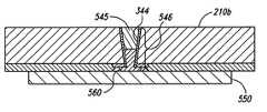
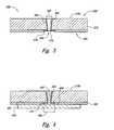
- FIG. 3is a schematic cross-sectional view of the microelectronic device 210 b taken substantially along line 3 - 3 in FIG. 2 in accordance with an embodiment of the invention.
- the microelectronic device 210 bis inverted in FIG. 3 for purposes of illustration, and it has undergone additional processing beyond that illustrated in FIG. 2 .
- the microelectronic device 210 bincludes a via or passage 342 extending through the die 212 and the bond-pad 216 .
- the passage 342 and the opening 218define a first opening 346 in the front side 201 of the microfeature workpiece 200 , and a second opening 348 in the back side 202 .
- the passage 342can be formed using a laser-cutting method at least generally similar to one or more of the methods described in co-pending U.S. patent application Ser. No. 10/713,878, entitled MICROELECTRONIC DEVICES, METHODS FOR FORMING VIAS IN MICROELECTRONIC DEVICES, AND METHODS FOR PACKAGING MICROELECTRONIC DEVICES.
- the passage 342can be formed using other methods, such as a suitable etching or drilling method.
- the passage 342may be slightly tapered as depicted in FIG. 3 , in other embodiments, the passage 342 can be straight or at least approximately straight.
- a dielectric layer 344can be applied to the inner wall of the passage 342 .
- the dielectric layer 344is an oxide applied in a low temperature chemical vapor deposition (CVD) process.
- the dielectric layer 344is a polyamide material or other materials suitable for insulating the die 212 from electrical leakage after the passage 342 has been filled with conductive metal (not shown) as described in greater detail below.
- FIG. 4is a schematic cross-sectional view illustrating a method of forming a conductive interconnect in the microelectronic device 210 b of FIG. 3 in accordance with an embodiment of the invention.
- a conductive element 450is positioned against the passivation layer 240 so that a contact surface 451 at least generally covers the first opening 346 of the passage 342 . Once the conductive element 450 is in this position, the passage 342 can be filled with conductive material 445 to form a conductive interconnect 446 extending through the microelectronic device 210 b .
- the conductive element 450is a conductive polymer that can be biased at an electrical potential to electroplate the conductive material 445 in the passage 342 .
- the conductive material 445can be copper or other conductive metals, such as silver, gold, palladium, etc. In still further embodiments, other conductive materials that can be deposited at low temperatures of 250° C. or less to fill the passage 342 .
- One shortcoming associated with the method described above with reference to FIG. 4is that occasionally the conductive element 450 allows some of the conductive material 445 to leak out of the first opening 346 and flow between the contact surface 451 and the passivation layer 240 . This leaked material can extend between two or more bond-pads 216 ( FIG. 2 ) and cause undesirable shorting between the bond-pads 216 .
- FIGS. 5A-5Bare schematic cross-sectional views illustrating various stages in a method of forming a conductive interconnect in the microelectronic device 210 b of FIG. 3 in accordance with another embodiment of the invention.
- this methodstarts with the microelectronic device 210 b configured as shown in FIG. 3 .
- a conductive plug 560is formed in the passage 342 adjacent to the bond-pad 216 .
- the conductive plug 560can be formed with conductive material that fills a portion of the passage 342 and electrically couples to an exposed surface of the bond-pad 216 that is not insulated by the dielectric layer 344 .
- the conductive plug 560can be formed by depositing an electrically conductive material in the passage 342 using a maskless mesoscale materials deposition process.
- a maskless mesoscale materials deposition processincludes the M 3 D technology offered by Optomec, Inc., of 3911 Singer Boulevard NE, Albuquerque, N. Mex. 87109.
- the conductive plug 560can be formed using other suitable methods.
- the conductive plug 560can include an electronic ink applied to the passage 342 using an electronic printing process.
- the conductive plug 560can be formed by depositing electrically conductive material in the passage 342 using a nano-particle deposition process.
- the conductive plug 560can include silver. In other embodiments, the conductive plug 560 can include other electrically conductive materials, such as gold, copper, palladium and/or various solders. Such materials can include those that can be deposited and/or printed in a conductive ink or paste at a low temperature, such as 250° C. or less.
- the remaining portion of the passage 342can be filled with a conductive material 545 to form a conductive interconnect 546 extending through the microelectronic device 210 b .
- the conductive plug 560can serve as an electrode for electroplating the passage 342 with a suitable material, such as copper.
- a conductive element 550is positioned against the conductive plug 560 and biased at an electrical potential to electroplate the conductive material 545 within the passage 342 .
- other methodscan be used to bias the conductive plug 560 at an electrical potential suitable for electroplating material into the passage 342 .
- FIGS. 6A-6Dare schematic cross-sectional views illustrating various stages in a method of forming a conductive interconnect in a microelectronic device 610 in accordance with an embodiment of the invention.
- the microelectronic device 610can include a die 612 having a through-hole or passage 642 .
- the passage 642defines a first opening 636 in a first side 601 of the microelectronic device 610 and a second opening 638 in a second side 602 .
- a passivation layer 644covers the die 612 including the inner wall of the passage 642 .
- the passivation layer 644can be tetraethylorthosilicate (TEOS) deposited using a low temperature CVD process.
- the passivation layer 644can be parylene and/or other suitable materials, such as silicon dioxide (SiO 2 ) or silicon nitrite (Si 3 N 4 ).
- TEOStetraethylorthosilicate
- the passivation layer 644can be parylene and/or other suitable materials, such as silicon dioxide (SiO 2 ) or silicon nitrite (Si 3 N 4 ).
- a tape, film, or other type of suitable sealing layer 670can be temporarily applied to the die 612 to at least generally seal the first opening 636 of the passage 642 .
- a first portion of conductive materialis deposited through the second opening 638 to form a plug 660 in the passage 642 adjacent to the sealing layer 670 .
- forming the plug 660can include depositing an electrically conductive material in the passage using a maskless mesoscale materials deposition process as described above with reference to FIG. 5A .
- forming the plug 660can include applying an electronic ink in the passage 642 using an electronic printing process.
- forming the plug 660can include depositing an electrically conductive material in the passage 642 using a nano-particle deposition process to deposit silver or other suitable metal.
- the sealing layer 670( FIG. 6B ) is removed from the microelectronic device 610 , and a conductive element 650 is positioned against the microelectronic device 610 so that a contact surface 651 makes electrical contact with the plug 660 .
- the conductive element 650can include an electrode configured to bias the plug 660 at an electrical potential for electroplating the passage 642 with a second portion of conductive material 645 to form a conductive interconnect 646 extending through the microelectronic device 610 .
- processing stepscan include removing the passivation layer 644 ( FIG. 6A ) from a first surface 631 of the die 612 , and forming a bond-pad 616 on the die 612 electrically coupled to the conductive interconnect 646 .
- other processing stepscan be employed to configure the microelectronic device 610 in a suitable form for subsequent use in a microelectronic device set or product.
- FIGS. 7A-7Bare schematic cross-sectional views illustrating various stages in a method of forming a conductive interconnect in the microelectronic device 610 in accordance with an embodiment of the invention that is similar to the embodiment described above with reference to FIGS. 6A-6D .
- the sealing layer 670FIG. 6B
- a metallic layer 780is deposited on the passivation layer 644 in electrical contact with the plug 660 .
- the metallic layer 780can be a metal layer formed by physical vapor deposition (PVD).
- the metallic layer 780can include other materials formed by other processes, such as a suitable CVD process.
- the conductive element 650is positioned against the metallic layer 780 .
- the conductive element 650can be a plate electrode or a conductive polymer configured to apply an electrical bias to the metallic layer 780 , which in turn biases the plug 660 .
- the conductive element 650can be a finger type contact as shown in U.S. Pat. No. 6,080,291, which is herein incorporated by reference. Electrically biasing the plug 660 facilitates electroplating a second portion of conductive material 745 in the passage 642 adjacent to the plug 660 . Together, the plug 660 and the second portion of conductive material 745 form a conductive interconnect 746 extending through the microelectronic device 610 .
- FIGS. 7C-7Dare schematic cross-sectional views illustrating various stages in a method of forming a bond-pad electrically coupled to the plug 660 in accordance with an embodiment of the invention.
- a resist layer 790is formed on the metallic layer 780 , and an opening 718 is formed in the resist layer 790 adjacent to the plug 660 .
- a metallic portion 792is then deposited on the metallic layer 780 through the opening 718 by using the metallic layer 780 as a seed layer. After depositing the metallic portion 792 , the resist layer 790 is removed as shown in FIG. 7D .
- all of the metallic layer 780is also removed (for example, by a suitable etching process). Together, the remaining metallic layer 780 and metallic portion 792 form a bond-pad 716 electrically coupled to the plug 660 .
- a suitable etching processfor example, by a suitable etching process.
- FIG. 8is a schematic cross-sectional view illustrating a method of forming a conductive interconnect in the microelectronic device 210 b of FIG. 3 using solder tent technology in accordance with a further embodiment of the invention.
- This methodstarts with the microelectronic device 210 b configured as shown in FIG. 3 .
- a metallic material 868is applied to the bond pad 216 by plating or another suitable process.
- the bond pad 216can be Aluminum (Al) and the metallic material 868 can be Nickel (Ni) that acts as a wetting agent to help subsequent material applications adhere to the bond pad 216 .
- a conductive plug 860is formed to fill a portion of the passage 342 and electrically couple to the bond-pad 216 .
- the conductive plug 860can be formed by depositing an electrically conductive material in the passage 342 using solder tent technology.
- the conductive plugcan include Tin-Lead (SnPb), Tin-Silver-Copper (SnAgCu), Tin-Cu (SnCu), or Tin-Silver (SnAg) material, among others.
- the remaining portion of the passage 342can be filled with a conductive material using one or more of the methods described above (such as the method described above with reference to FIG. 5B ) to form a conductive interconnect 846 extending through the microelectronic device 210 b.
- FIG. 9schematically illustrates a microelectronic device set comprised of the first microelectronic device 210 b and a second microelectronic device 920 .
- the second microelectronic device 920includes a second die 912 with a second integrated circuit 914 electrically coupled to a second bond-pad 916 .
- the second bond pad 916can be electrically coupled to the conductive interconnect 546 and the first bond pad 216 by, for example, re-melting or reflowing a portion of the conductive plug 560 and/or using other suitable connection methods known in the art.
Landscapes
- Engineering & Computer Science (AREA)
- Microelectronics & Electronic Packaging (AREA)
- Power Engineering (AREA)
- Computer Hardware Design (AREA)
- Physics & Mathematics (AREA)
- Condensed Matter Physics & Semiconductors (AREA)
- General Physics & Mathematics (AREA)
- Manufacturing & Machinery (AREA)
- Internal Circuitry In Semiconductor Integrated Circuit Devices (AREA)
Abstract
Description
Claims (20)
Priority Applications (5)
| Application Number | Priority Date | Filing Date | Title |
|---|---|---|---|
| US10/733,226US8084866B2 (en) | 2003-12-10 | 2003-12-10 | Microelectronic devices and methods for filling vias in microelectronic devices |
| US13/337,943US8748311B2 (en) | 2003-12-10 | 2011-12-27 | Microelectronic devices and methods for filing vias in microelectronic devices |
| US14/300,004US9653420B2 (en) | 2003-11-13 | 2014-06-09 | Microelectronic devices and methods for filling vias in microelectronic devices |
| US15/583,500US20170301639A1 (en) | 2003-12-10 | 2017-05-01 | Microelectronic devices and methods for filling vias in microelectronic devices |
| US16/055,492US11177175B2 (en) | 2003-12-10 | 2018-08-06 | Microelectronic devices and methods for filling vias in microelectronic devices |
Applications Claiming Priority (1)
| Application Number | Priority Date | Filing Date | Title |
|---|---|---|---|
| US10/733,226US8084866B2 (en) | 2003-12-10 | 2003-12-10 | Microelectronic devices and methods for filling vias in microelectronic devices |
Related Child Applications (1)
| Application Number | Title | Priority Date | Filing Date |
|---|---|---|---|
| US13/337,943DivisionUS8748311B2 (en) | 2003-11-13 | 2011-12-27 | Microelectronic devices and methods for filing vias in microelectronic devices |
Publications (2)
| Publication Number | Publication Date |
|---|---|
| US20050127478A1 US20050127478A1 (en) | 2005-06-16 |
| US8084866B2true US8084866B2 (en) | 2011-12-27 |
Family
ID=34653053
Family Applications (5)
| Application Number | Title | Priority Date | Filing Date |
|---|---|---|---|
| US10/733,226Active2026-06-07US8084866B2 (en) | 2003-11-13 | 2003-12-10 | Microelectronic devices and methods for filling vias in microelectronic devices |
| US13/337,943Expired - LifetimeUS8748311B2 (en) | 2003-11-13 | 2011-12-27 | Microelectronic devices and methods for filing vias in microelectronic devices |
| US14/300,004Expired - Fee RelatedUS9653420B2 (en) | 2003-11-13 | 2014-06-09 | Microelectronic devices and methods for filling vias in microelectronic devices |
| US15/583,500AbandonedUS20170301639A1 (en) | 2003-12-10 | 2017-05-01 | Microelectronic devices and methods for filling vias in microelectronic devices |
| US16/055,492Expired - LifetimeUS11177175B2 (en) | 2003-12-10 | 2018-08-06 | Microelectronic devices and methods for filling vias in microelectronic devices |
Family Applications After (4)
| Application Number | Title | Priority Date | Filing Date |
|---|---|---|---|
| US13/337,943Expired - LifetimeUS8748311B2 (en) | 2003-11-13 | 2011-12-27 | Microelectronic devices and methods for filing vias in microelectronic devices |
| US14/300,004Expired - Fee RelatedUS9653420B2 (en) | 2003-11-13 | 2014-06-09 | Microelectronic devices and methods for filling vias in microelectronic devices |
| US15/583,500AbandonedUS20170301639A1 (en) | 2003-12-10 | 2017-05-01 | Microelectronic devices and methods for filling vias in microelectronic devices |
| US16/055,492Expired - LifetimeUS11177175B2 (en) | 2003-12-10 | 2018-08-06 | Microelectronic devices and methods for filling vias in microelectronic devices |
Country Status (1)
| Country | Link |
|---|---|
| US (5) | US8084866B2 (en) |
Cited By (12)
| Publication number | Priority date | Publication date | Assignee | Title |
|---|---|---|---|---|
| US20100213592A1 (en)* | 2009-02-24 | 2010-08-26 | International Business Machines Corporation | Semiconductor Module, Terminal Strip, Method for Manufacturing Terminal Strip, and Method for Manufacturing Semiconductor Module |
| US20110089571A1 (en)* | 2009-10-15 | 2011-04-21 | Seiko Epson Corporation | Semiconductor device, circuit substrate, and electronic device |
| US20120164787A1 (en)* | 2010-12-23 | 2012-06-28 | Electronics And Telecommunications Research Institute | Vacuum wafer level packaging method for micro electro mechanical system device |
| US20120292763A1 (en)* | 2010-02-09 | 2012-11-22 | International Business Machines Corporation | Electromigration immune through-substrate vias |
| US20130119547A1 (en)* | 2011-11-15 | 2013-05-16 | Samsung Electronics Co., Ltd. | Integrated circuit device including through-silicon via structure having offset interface |
| US8748311B2 (en) | 2003-12-10 | 2014-06-10 | Micron Technology, Inc. | Microelectronic devices and methods for filing vias in microelectronic devices |
| US20150054172A1 (en)* | 2013-08-21 | 2015-02-26 | Kabushiki Kaisha Toshiba | Semiconductor device and method of manufacturing the same |
| US20150263647A1 (en)* | 2014-03-15 | 2015-09-17 | Canon Kabushiki Kaisha | Device having element electrode connected to penetrating wire, and method for manufacturing the same |
| US9153522B2 (en) | 2012-09-25 | 2015-10-06 | Samsung Electronics Co., Ltd. | Semiconductor devices and methods of fabricating the same |
| US20170231092A1 (en)* | 2007-06-28 | 2017-08-10 | Intel Corporation | Method of forming a substrate core structure using microvia laser drilling and conductive layer pre-patterning and substrate core structure formed according to the method |
| US20170323828A1 (en)* | 2005-09-01 | 2017-11-09 | Micron Technology, Inc. | Microfeature workpieces and methods for forming interconnects in microfeature workpieces |
| US20200006272A1 (en)* | 2018-06-29 | 2020-01-02 | Andreas Augustin | Through-silicon via pillars for connecting dice and methods of assembling same |
Families Citing this family (79)
| Publication number | Priority date | Publication date | Assignee | Title |
|---|---|---|---|---|
| US6934065B2 (en)* | 2003-09-18 | 2005-08-23 | Micron Technology, Inc. | Microelectronic devices and methods for packaging microelectronic devices |
| US7091124B2 (en) | 2003-11-13 | 2006-08-15 | Micron Technology, Inc. | Methods for forming vias in microelectronic devices, and methods for packaging microelectronic devices |
| US20050104171A1 (en)* | 2003-11-13 | 2005-05-19 | Benson Peter A. | Microelectronic devices having conductive complementary structures and methods of manufacturing microelectronic devices having conductive complementary structures |
| US7583862B2 (en)* | 2003-11-26 | 2009-09-01 | Aptina Imaging Corporation | Packaged microelectronic imagers and methods of packaging microelectronic imagers |
| US7253397B2 (en)* | 2004-02-23 | 2007-08-07 | Micron Technology, Inc. | Packaged microelectronic imagers and methods of packaging microelectronic imagers |
| EP1722613B1 (en)* | 2004-03-04 | 2011-11-23 | Sankyo Kasei Co., Ltd. | Method for manufacturing a three-dimensional circuit board |
| US20050247894A1 (en) | 2004-05-05 | 2005-11-10 | Watkins Charles M | Systems and methods for forming apertures in microfeature workpieces |
| US8092734B2 (en)* | 2004-05-13 | 2012-01-10 | Aptina Imaging Corporation | Covers for microelectronic imagers and methods for wafer-level packaging of microelectronics imagers |
| US7253957B2 (en)* | 2004-05-13 | 2007-08-07 | Micron Technology, Inc. | Integrated optics units and methods of manufacturing integrated optics units for use with microelectronic imagers |
| US20050275750A1 (en) | 2004-06-09 | 2005-12-15 | Salman Akram | Wafer-level packaged microelectronic imagers and processes for wafer-level packaging |
| US7498647B2 (en) | 2004-06-10 | 2009-03-03 | Micron Technology, Inc. | Packaged microelectronic imagers and methods of packaging microelectronic imagers |
| US7262405B2 (en)* | 2004-06-14 | 2007-08-28 | Micron Technology, Inc. | Prefabricated housings for microelectronic imagers |
| US7199439B2 (en)* | 2004-06-14 | 2007-04-03 | Micron Technology, Inc. | Microelectronic imagers and methods of packaging microelectronic imagers |
| US7232754B2 (en)* | 2004-06-29 | 2007-06-19 | Micron Technology, Inc. | Microelectronic devices and methods for forming interconnects in microelectronic devices |
| US7294897B2 (en)* | 2004-06-29 | 2007-11-13 | Micron Technology, Inc. | Packaged microelectronic imagers and methods of packaging microelectronic imagers |
| US7416913B2 (en)* | 2004-07-16 | 2008-08-26 | Micron Technology, Inc. | Methods of manufacturing microelectronic imaging units with discrete standoffs |
| US7189954B2 (en)* | 2004-07-19 | 2007-03-13 | Micron Technology, Inc. | Microelectronic imagers with optical devices and methods of manufacturing such microelectronic imagers |
| US7402453B2 (en)* | 2004-07-28 | 2008-07-22 | Micron Technology, Inc. | Microelectronic imaging units and methods of manufacturing microelectronic imaging units |
| US20060023107A1 (en)* | 2004-08-02 | 2006-02-02 | Bolken Todd O | Microelectronic imagers with optics supports having threadless interfaces and methods for manufacturing such microelectronic imagers |
| US7364934B2 (en)* | 2004-08-10 | 2008-04-29 | Micron Technology, Inc. | Microelectronic imaging units and methods of manufacturing microelectronic imaging units |
| US7223626B2 (en)* | 2004-08-19 | 2007-05-29 | Micron Technology, Inc. | Spacers for packaged microelectronic imagers and methods of making and using spacers for wafer-level packaging of imagers |
| US7397066B2 (en)* | 2004-08-19 | 2008-07-08 | Micron Technology, Inc. | Microelectronic imagers with curved image sensors and methods for manufacturing microelectronic imagers |
| US7425499B2 (en) | 2004-08-24 | 2008-09-16 | Micron Technology, Inc. | Methods for forming interconnects in vias and microelectronic workpieces including such interconnects |
| US7115961B2 (en)* | 2004-08-24 | 2006-10-03 | Micron Technology, Inc. | Packaged microelectronic imaging devices and methods of packaging microelectronic imaging devices |
| US7429494B2 (en)* | 2004-08-24 | 2008-09-30 | Micron Technology, Inc. | Microelectronic imagers with optical devices having integral reference features and methods for manufacturing such microelectronic imagers |
| US7276393B2 (en)* | 2004-08-26 | 2007-10-02 | Micron Technology, Inc. | Microelectronic imaging units and methods of manufacturing microelectronic imaging units |
| SG120200A1 (en) | 2004-08-27 | 2006-03-28 | Micron Technology Inc | Slanted vias for electrical circuits on circuit boards and other substrates |
| US7511262B2 (en)* | 2004-08-30 | 2009-03-31 | Micron Technology, Inc. | Optical device and assembly for use with imaging dies, and wafer-label imager assembly |
| US20070148807A1 (en)* | 2005-08-22 | 2007-06-28 | Salman Akram | Microelectronic imagers with integrated optical devices and methods for manufacturing such microelectronic imagers |
| US7646075B2 (en)* | 2004-08-31 | 2010-01-12 | Micron Technology, Inc. | Microelectronic imagers having front side contacts |
| US7279407B2 (en)* | 2004-09-02 | 2007-10-09 | Micron Technology, Inc. | Selective nickel plating of aluminum, copper, and tungsten structures |
| US7300857B2 (en) | 2004-09-02 | 2007-11-27 | Micron Technology, Inc. | Through-wafer interconnects for photoimager and memory wafers |
| KR100577430B1 (en) | 2004-09-03 | 2006-05-08 | 삼성전자주식회사 | Display device |
| US7271482B2 (en)* | 2004-12-30 | 2007-09-18 | Micron Technology, Inc. | Methods for forming interconnects in microelectronic workpieces and microelectronic workpieces formed using such methods |
| US7214919B2 (en)* | 2005-02-08 | 2007-05-08 | Micron Technology, Inc. | Microelectronic imaging units and methods of manufacturing microelectronic imaging units |
| US7303931B2 (en)* | 2005-02-10 | 2007-12-04 | Micron Technology, Inc. | Microfeature workpieces having microlenses and methods of forming microlenses on microfeature workpieces |
| US20060177999A1 (en)* | 2005-02-10 | 2006-08-10 | Micron Technology, Inc. | Microelectronic workpieces and methods for forming interconnects in microelectronic workpieces |
| US7190039B2 (en)* | 2005-02-18 | 2007-03-13 | Micron Technology, Inc. | Microelectronic imagers with shaped image sensors and methods for manufacturing microelectronic imagers |
| JP5048230B2 (en)* | 2005-03-30 | 2012-10-17 | オンセミコンダクター・トレーディング・リミテッド | Semiconductor device and manufacturing method thereof |
| US7795134B2 (en)* | 2005-06-28 | 2010-09-14 | Micron Technology, Inc. | Conductive interconnect structures and formation methods using supercritical fluids |
| US20060290001A1 (en)* | 2005-06-28 | 2006-12-28 | Micron Technology, Inc. | Interconnect vias and associated methods of formation |
| SG130061A1 (en)* | 2005-08-24 | 2007-03-20 | Micron Technology Inc | Microelectronic devices and microelectronic support devices, and associated assemblies and methods |
| JP4533283B2 (en)* | 2005-08-29 | 2010-09-01 | 新光電気工業株式会社 | Manufacturing method of semiconductor device |
| US8308053B2 (en) | 2005-08-31 | 2012-11-13 | Micron Technology, Inc. | Microfeature workpieces having alloyed conductive structures, and associated methods |
| US7288757B2 (en) | 2005-09-01 | 2007-10-30 | Micron Technology, Inc. | Microelectronic imaging devices and associated methods for attaching transmissive elements |
| US7262134B2 (en)* | 2005-09-01 | 2007-08-28 | Micron Technology, Inc. | Microfeature workpieces and methods for forming interconnects in microfeature workpieces |
| US7622377B2 (en) | 2005-09-01 | 2009-11-24 | Micron Technology, Inc. | Microfeature workpiece substrates having through-substrate vias, and associated methods of formation |
| JP5222459B2 (en)* | 2005-10-18 | 2013-06-26 | 新光電気工業株式会社 | Semiconductor chip manufacturing method, multichip package |
| US7749899B2 (en) | 2006-06-01 | 2010-07-06 | Micron Technology, Inc. | Microelectronic workpieces and methods and systems for forming interconnects in microelectronic workpieces |
| EP2024767A4 (en) | 2006-06-02 | 2010-08-04 | Electro Scient Ind Inc | Process for optically transparent via filling |
| US7968820B2 (en)* | 2006-06-02 | 2011-06-28 | Electro Scientific Industries, Inc. | Method of producing a panel having an area with light transmissivity |
| US7385283B2 (en)* | 2006-06-27 | 2008-06-10 | Taiwan Semiconductor Manufacturing Co., Ltd. | Three dimensional integrated circuit and method of making the same |
| US7446424B2 (en)* | 2006-07-19 | 2008-11-04 | Taiwan Semiconductor Manufacturing Co., Ltd. | Interconnect structure for semiconductor package |
| US7629249B2 (en) | 2006-08-28 | 2009-12-08 | Micron Technology, Inc. | Microfeature workpieces having conductive interconnect structures formed by chemically reactive processes, and associated systems and methods |
| US7902643B2 (en) | 2006-08-31 | 2011-03-08 | Micron Technology, Inc. | Microfeature workpieces having interconnects and conductive backplanes, and associated systems and methods |
| SE530415C2 (en)* | 2006-09-04 | 2008-05-27 | Nanospace Ab | Gastrustor |
| DE102007019552B4 (en)* | 2007-04-25 | 2009-12-17 | Infineon Technologies Ag | Method for producing a substrate with feedthrough and substrate and semiconductor module with feedthrough |
| US7886437B2 (en)* | 2007-05-25 | 2011-02-15 | Electro Scientific Industries, Inc. | Process for forming an isolated electrically conductive contact through a metal package |
| US8710402B2 (en)* | 2007-06-01 | 2014-04-29 | Electro Scientific Industries, Inc. | Method of and apparatus for laser drilling holes with improved taper |
| SG149710A1 (en) | 2007-07-12 | 2009-02-27 | Micron Technology Inc | Interconnects for packaged semiconductor devices and methods for manufacturing such devices |
| SG150410A1 (en) | 2007-08-31 | 2009-03-30 | Micron Technology Inc | Partitioned through-layer via and associated systems and methods |
| US8220142B2 (en)* | 2007-10-03 | 2012-07-17 | Apple Inc. | Method of forming a housing component |
| US7884015B2 (en) | 2007-12-06 | 2011-02-08 | Micron Technology, Inc. | Methods for forming interconnects in microelectronic workpieces and microelectronic workpieces formed using such methods |
| US8084854B2 (en) | 2007-12-28 | 2011-12-27 | Micron Technology, Inc. | Pass-through 3D interconnect for microelectronic dies and associated systems and methods |
| US7884488B2 (en)* | 2008-05-01 | 2011-02-08 | Qimonda Ag | Semiconductor component with improved contact pad and method for forming the same |
| US8253230B2 (en) | 2008-05-15 | 2012-08-28 | Micron Technology, Inc. | Disabling electrical connections using pass-through 3D interconnects and associated systems and methods |
| JP2010040862A (en)* | 2008-08-06 | 2010-02-18 | Fujikura Ltd | Semiconductor device |
| US7872332B2 (en) | 2008-09-11 | 2011-01-18 | Micron Technology, Inc. | Interconnect structures for stacked dies, including penetrating structures for through-silicon vias, and associated systems and methods |
| US8367516B2 (en)* | 2009-01-14 | 2013-02-05 | Taiwan Semiconductor Manufacturing Company, Ltd. | Laser bonding for stacking semiconductor substrates |
| US20100194465A1 (en)* | 2009-02-02 | 2010-08-05 | Ali Salih | Temperature compensated current source and method therefor |
| US8524127B2 (en)* | 2010-03-26 | 2013-09-03 | Electro Scientific Industries, Inc. | Method of manufacturing a panel with occluded microholes |
| US9640437B2 (en) | 2010-07-23 | 2017-05-02 | Tessera, Inc. | Methods of forming semiconductor elements using micro-abrasive particle stream |
| US8803316B2 (en) | 2011-12-06 | 2014-08-12 | Taiwan Semiconductor Manufacturing Company, Ltd. | TSV structures and methods for forming the same |
| US9159699B2 (en)* | 2012-11-13 | 2015-10-13 | Delta Electronics, Inc. | Interconnection structure having a via structure |
| WO2017179104A1 (en)* | 2016-04-11 | 2017-10-19 | オリンパス株式会社 | Semiconductor element bonding structure, image pickup module, and endoscope device |
| JP2018163918A (en)* | 2017-03-24 | 2018-10-18 | 新光電気工業株式会社 | Wiring board and method of manufacturing the same |
| US10777562B1 (en)* | 2019-03-14 | 2020-09-15 | Micron Technology, Inc. | Integrated circuity, DRAM circuitry, methods used in forming integrated circuitry, and methods used in forming DRAM circuitry |
| KR102821727B1 (en) | 2020-08-03 | 2025-06-19 | 삼성전자주식회사 | Semiconductor device and semiconductor package |
| US11551926B2 (en)* | 2021-01-22 | 2023-01-10 | Micron Technology, Inc. | Methods of forming a microelectronic device, and related systems and additional methods |
Citations (494)
| Publication number | Priority date | Publication date | Assignee | Title |
|---|---|---|---|---|
| US2821959A (en) | 1956-03-29 | 1958-02-04 | Bell Telephone Labor Inc | Mass soldering of electrical assemblies |
| US3006318A (en) | 1958-03-26 | 1961-10-31 | Western Electric Co | Apparatus for applying solder coatings to surfaces |
| US3345134A (en) | 1962-04-21 | 1967-10-03 | Knapsack Ag | Process and apparatus for the manufacture of titanium nitride |
| US3865298A (en) | 1973-08-14 | 1975-02-11 | Atomic Energy Commission | Solder leveling |
| US3902036A (en) | 1974-05-02 | 1975-08-26 | Western Electric Co | Control system using multiplexed laser beams |
| US4040168A (en) | 1975-11-24 | 1977-08-09 | Rca Corporation | Fabrication method for a dual gate field-effect transistor |
| US4368106A (en) | 1980-10-27 | 1983-01-11 | General Electric Company | Implantation of electrical feed-through conductors |
| EP0127946A1 (en) | 1983-05-10 | 1984-12-12 | BRITISH TELECOMMUNICATIONS public limited company | Method of producing a via in a semiconductor device |
| US4534100A (en) | 1982-06-28 | 1985-08-13 | The United States Of America As Represented By The Secretary Of The Air Force | Electrical method of making conductive paths in silicon |
| US4581301A (en) | 1984-04-10 | 1986-04-08 | Michaelson Henry W | Additive adhesive based process for the manufacture of printed circuit boards |
| US4608480A (en) | 1983-06-15 | 1986-08-26 | S.N.E.C.M.A. | Process and apparatus for laser drilling |
| US4614427A (en) | 1983-05-20 | 1986-09-30 | Hitachi, Ltd. | Automatic contaminants detection apparatus |
| US4627971A (en) | 1985-04-22 | 1986-12-09 | Alza Corporation | Osmotic device with self-sealing passageway |
| US4660063A (en) | 1985-03-18 | 1987-04-21 | General Electric Company | Immersion type ISFET |
| US4700473A (en)* | 1986-01-03 | 1987-10-20 | Motorola Inc. | Method of making an ultra high density pad array chip carrier |
| US4756765A (en) | 1982-01-26 | 1988-07-12 | Avco Research Laboratory, Inc. | Laser removal of poor thermally-conductive materials |
| US4768291A (en) | 1987-03-12 | 1988-09-06 | Monarch Technologies Corporation | Apparatus for dry processing a semiconductor wafer |
| US4818728A (en) | 1986-12-03 | 1989-04-04 | Sharp Kabushiki Kaisha | Method of making a hybrid semiconductor device |
| US4907127A (en) | 1988-03-21 | 1990-03-06 | Lee John K C | Printed circuit board construction and method for producing printed circuit end products |
| US4959705A (en) | 1988-10-17 | 1990-09-25 | Ford Microelectronics, Inc. | Three metal personalization of application specific monolithic microwave integrated circuit |
| US4964212A (en) | 1988-09-29 | 1990-10-23 | Commissariat A L'energie Atomique | Process for producing electrical connections through a substrate |
| US4984597A (en) | 1984-05-21 | 1991-01-15 | Cfm Technologies Research Associates | Apparatus for rinsing and drying surfaces |
| US5024966A (en) | 1988-12-21 | 1991-06-18 | At&T Bell Laboratories | Method of forming a silicon-based semiconductor optical device mount |
| US5026964A (en) | 1986-02-28 | 1991-06-25 | General Electric Company | Optical breakthrough sensor for laser drill |
| US5027184A (en) | 1981-03-02 | 1991-06-25 | Rockwell International Corporation | NPN type lateral transistor with minimal substrate operation interference |
| US5037782A (en) | 1989-03-29 | 1991-08-06 | Mitsubishi Denki Kabushiki Kaisha | Method of making a semiconductor device including via holes |
| US5107328A (en) | 1991-02-13 | 1992-04-21 | Micron Technology, Inc. | Packaging means for a semiconductor die having particular shelf structure |
| US5123902A (en) | 1988-09-13 | 1992-06-23 | Carl-Zeiss-Stiftung | Method and apparatus for performing surgery on tissue wherein a laser beam is applied to the tissue |
| US5128831A (en) | 1991-10-31 | 1992-07-07 | Micron Technology, Inc. | High-density electronic package comprising stacked sub-modules which are electrically interconnected by solder-filled vias |
| US5138434A (en) | 1991-01-22 | 1992-08-11 | Micron Technology, Inc. | Packaging for semiconductor logic devices |
| US5145099A (en) | 1990-07-13 | 1992-09-08 | Micron Technology, Inc. | Method for combining die attach and lead bond in the assembly of a semiconductor package |
| US5158911A (en) | 1990-08-03 | 1992-10-27 | Thomson Composants Microondes | Method for interconnection between an integrated circuit and a support circuit, and integrated circuit adapted to this method |
| US5219344A (en) | 1988-06-09 | 1993-06-15 | Visx, Incorporated | Methods and apparatus for laser sculpture of the cornea |
| US5233448A (en) | 1992-05-04 | 1993-08-03 | Industrial Technology Research Institute | Method of manufacturing a liquid crystal display panel including photoconductive electrostatic protection |
| US5237148A (en) | 1990-10-04 | 1993-08-17 | Brother Kogyo Kabushiki | Device for manufacturing a nozzle and its manufacturing method |
| US5252857A (en) | 1991-08-05 | 1993-10-12 | International Business Machines Corporation | Stacked DCA memory chips |
| US5289631A (en) | 1992-03-04 | 1994-03-01 | Mcnc | Method for testing, burn-in, and/or programming of integrated circuit chips |
| US5292686A (en) | 1991-08-21 | 1994-03-08 | Triquint Semiconductor, Inc. | Method of forming substrate vias in a GaAs wafer |
| US5294568A (en) | 1990-10-12 | 1994-03-15 | Genus, Inc. | Method of selective etching native oxide |
| US5304743A (en) | 1992-05-12 | 1994-04-19 | Lsi Logic Corporation | Multilayer IC semiconductor package |
| US5378313A (en) | 1993-12-22 | 1995-01-03 | Pace; Benedict G. | Hybrid circuits and a method of manufacture |
| US5378312A (en) | 1993-12-07 | 1995-01-03 | International Business Machines Corporation | Process for fabricating a semiconductor structure having sidewalls |
| US5380681A (en) | 1994-03-21 | 1995-01-10 | United Microelectronics Corporation | Three-dimensional multichip package and methods of fabricating |
| US5402435A (en) | 1993-03-05 | 1995-03-28 | Matsushita Electric Industrial Co., Ltd. | Optical device |
| US5406630A (en) | 1992-05-04 | 1995-04-11 | Motorola, Inc. | Tamperproof arrangement for an integrated circuit device |
| US5424573A (en) | 1992-03-04 | 1995-06-13 | Hitachi, Ltd. | Semiconductor package having optical interconnection access |
| TW250597B (en) | 1993-06-04 | 1995-07-01 | Framatome & Cie | |
| US5438212A (en) | 1993-02-25 | 1995-08-01 | Mitsubishi Denki Kabushiki Kaisha | Semiconductor device with heat dissipation structure |
| US5447871A (en) | 1993-03-05 | 1995-09-05 | Goldstein; Edward F. | Electrically conductive interconnection through a body of semiconductor material |
| US5464960A (en) | 1993-01-12 | 1995-11-07 | Iatrotech, Inc. | Laser calibration device |
| US5481483A (en) | 1992-11-23 | 1996-01-02 | Ford Motor Company | Non-contact method of obtaining dimensional information about an object for comparing similar objects |
| US5496755A (en) | 1989-11-29 | 1996-03-05 | Texas Instruments Incorporated | Integrated circuit and method |
| US5515167A (en) | 1994-09-13 | 1996-05-07 | Hughes Aircraft Company | Transparent optical chuck incorporating optical monitoring |
| US5518957A (en) | 1991-10-10 | 1996-05-21 | Samsung Electronics Co., Ltd. | Method for making a thin profile semiconductor package |
| US5518956A (en) | 1993-09-02 | 1996-05-21 | General Electric Company | Method of isolating vertical shorts in an electronic array using laser ablation |
| US5585308A (en) | 1993-12-23 | 1996-12-17 | Sgs-Thomson Microelectronics, Inc. | Method for improved pre-metal planarization |
| US5585675A (en) | 1994-05-11 | 1996-12-17 | Harris Corporation | Semiconductor die packaging tub having angularly offset pad-to-pad via structure configured to allow three-dimensional stacking and electrical interconnections among multiple identical tubs |
| US5593927A (en) | 1993-10-14 | 1997-01-14 | Micron Technology, Inc. | Method for packaging semiconductor dice |
| US5614743A (en) | 1994-07-26 | 1997-03-25 | Kabushiki Kaisha Toshiba | Microwave integrated circuit (MIC) having a reactance element formed on a groove |
| US5618752A (en) | 1995-06-05 | 1997-04-08 | Harris Corporation | Method of fabrication of surface mountable integrated circuits |
| US5624437A (en) | 1995-03-28 | 1997-04-29 | Freeman; Jerre M. | High resolution, high speed, programmable laser beam modulating apparatus for microsurgery |
| US5627106A (en) | 1994-05-06 | 1997-05-06 | United Microelectronics Corporation | Trench method for three dimensional chip connecting during IC fabrication |
| US5646067A (en) | 1995-06-05 | 1997-07-08 | Harris Corporation | Method of bonding wafers having vias including conductive material |
| US5654221A (en) | 1994-10-17 | 1997-08-05 | International Business Machines Corporation | Method for forming semiconductor chip and electronic module with integrated surface interconnects/components |
| US5673846A (en) | 1995-08-24 | 1997-10-07 | International Business Machines Corporation | Solder anchor decal and method |
| US5677566A (en) | 1995-05-08 | 1997-10-14 | Micron Technology, Inc. | Semiconductor chip package |
| US5684642A (en) | 1994-02-22 | 1997-11-04 | Mitsubishi Denki Kabushiki Kaisha | Optical transmission system and light radiating method |
| US5690841A (en) | 1993-12-10 | 1997-11-25 | Pharmacia Biotech Ab | Method of producing cavity structures |
| US5718791A (en) | 1995-06-05 | 1998-02-17 | R + S Stanztechnik Gmbh | Method of laminating a trim panel and folding a cover sheet edge around the panel rim |
| US5723904A (en) | 1993-03-10 | 1998-03-03 | Sumitomo Electric Industries, Ltd. | Packaged semiconductor device suitable to be mounted and connected to microstrip line structure board |
| US5726493A (en) | 1994-06-13 | 1998-03-10 | Fujitsu Limited | Semiconductor device and semiconductor device unit having ball-grid-array type package structure |
| US5771158A (en) | 1995-09-21 | 1998-06-23 | Mitsubishi Denki Kabushiki Kaisha | Printed circuit board, printed circuit board used for flat panel display drive circuit, and flat panel display device |
| US5773359A (en) | 1995-12-26 | 1998-06-30 | Motorola, Inc. | Interconnect system and method of fabrication |
| US5776824A (en) | 1995-12-22 | 1998-07-07 | Micron Technology, Inc. | Method for producing laminated film/metal structures for known good die ("KG") applications |
| US5807439A (en) | 1997-09-29 | 1998-09-15 | Siemens Aktiengesellschaft | Apparatus and method for improved washing and drying of semiconductor wafers |
| US5811799A (en) | 1997-07-31 | 1998-09-22 | Wu; Liang-Chung | Image sensor package having a wall with a sealed cover |
| US5821532A (en) | 1997-06-16 | 1998-10-13 | Eastman Kodak Company | Imager package substrate |
| US5825080A (en) | 1995-12-18 | 1998-10-20 | Atr Optical And Radio Communications Research Laboratories | Semiconductor device provided with surface grounding conductor for covering surfaces of electrically insulating films |
| US5826628A (en) | 1996-01-24 | 1998-10-27 | Micron Technology, Inc. | Form tooling and method of forming semiconductor package leads |
| US5847454A (en) | 1993-02-04 | 1998-12-08 | Cornell Research Foundcatton, Inc. | Electrically isolated released microstructures |
| US5851845A (en) | 1995-12-18 | 1998-12-22 | Micron Technology, Inc. | Process for packaging a semiconductor die using dicing and testing |
| US5857963A (en) | 1996-07-17 | 1999-01-12 | Welch Allyn, Inc. | Tab imager assembly for use in an endoscope |
| US5861654A (en) | 1995-11-28 | 1999-01-19 | Eastman Kodak Company | Image sensor assembly |
| US5870289A (en) | 1994-12-15 | 1999-02-09 | Hitachi, Ltd. | Chip connection structure having diret through-hole connections through adhesive film and wiring substrate |
| US5870823A (en) | 1996-11-27 | 1999-02-16 | International Business Machines Corporation | Method of forming a multilayer electronic packaging substrate with integral cooling channels |
| US5883426A (en) | 1996-04-18 | 1999-03-16 | Nec Corporation | Stack module |
| US5891797A (en) | 1997-10-20 | 1999-04-06 | Micron Technology, Inc. | Method of forming a support structure for air bridge wiring of an integrated circuit |
| US5893828A (en) | 1996-05-02 | 1999-04-13 | Uram; Martin | Contact laser surgical endoscope and associated myringotomy procedure |
| US5904499A (en) | 1994-12-22 | 1999-05-18 | Pace; Benedict G | Package for power semiconductor chips |
| US5925930A (en) | 1996-05-21 | 1999-07-20 | Micron Technology, Inc. | IC contacts with palladium layer and flexible conductive epoxy bumps |
| US5933713A (en) | 1998-04-06 | 1999-08-03 | Micron Technology, Inc. | Method of forming overmolded chip scale package and resulting product |
| US5938956A (en) | 1996-09-10 | 1999-08-17 | Micron Technology, Inc. | Circuit and method for heating an adhesive to package or rework a semiconductor die |
| US5946553A (en) | 1991-06-04 | 1999-08-31 | Micron Technology, Inc. | Process for manufacturing a semiconductor package with bi-substrate die |
| US5969422A (en) | 1997-05-15 | 1999-10-19 | Advanced Micro Devices, Inc. | Plated copper interconnect structure |
| US5986209A (en) | 1997-07-09 | 1999-11-16 | Micron Technology, Inc. | Package stack via bottom leaded plastic (BLP) packaging |
| US5990566A (en) | 1998-05-20 | 1999-11-23 | Micron Technology, Inc. | High density semiconductor package |
| US5998240A (en) | 1996-07-22 | 1999-12-07 | Northrop Grumman Corporation | Method of extracting heat from a semiconductor body and forming microchannels therein |
| US5998292A (en) | 1997-11-12 | 1999-12-07 | International Business Machines Corporation | Method for making three dimensional circuit integration |
| US6004867A (en) | 1996-12-16 | 1999-12-21 | Samsung Electronics Co., Ltd. | Chip-size packages assembled using mass production techniques at the wafer-level |
| US6008914A (en) | 1994-04-28 | 1999-12-28 | Mitsubishi Denki Kabushiki Kaisha | Laser transfer machining apparatus |
| US6008070A (en) | 1998-05-21 | 1999-12-28 | Micron Technology, Inc. | Wafer level fabrication and assembly of chip scale packages |
| US6018249A (en) | 1997-12-11 | 2000-01-25 | Micron Technolgoy, Inc. | Test system with mechanical alignment for semiconductor chip scale packages and dice |
| US6020629A (en) | 1998-06-05 | 2000-02-01 | Micron Technology, Inc. | Stacked semiconductor package and method of fabrication |
| US6028365A (en) | 1998-03-30 | 2000-02-22 | Micron Technology, Inc. | Integrated circuit package and method of fabrication |
| US6048755A (en) | 1998-11-12 | 2000-04-11 | Micron Technology, Inc. | Method for fabricating BGA package using substrate with patterned solder mask open in die attach area |
| US6051878A (en) | 1997-03-10 | 2000-04-18 | Micron Technology, Inc. | Method of constructing stacked packages |
| US6066514A (en) | 1996-10-18 | 2000-05-23 | Micron Technology, Inc. | Adhesion enhanced semiconductor die for mold compound packaging |
| US6072236A (en) | 1996-03-07 | 2000-06-06 | Micron Technology, Inc. | Micromachined chip scale package |
| US6072233A (en) | 1998-05-04 | 2000-06-06 | Micron Technology, Inc. | Stackable ball grid array package |
| US6080291A (en) | 1998-07-10 | 2000-06-27 | Semitool, Inc. | Apparatus for electrochemically processing a workpiece including an electrical contact assembly having a seal member |
| US6081429A (en) | 1999-01-20 | 2000-06-27 | Micron Technology, Inc. | Test interposer for use with ball grid array packages assemblies and ball grid array packages including same and methods |
| US6089920A (en) | 1998-05-04 | 2000-07-18 | Micron Technology, Inc. | Modular die sockets with flexible interconnects for packaging bare semiconductor die |
| US6097087A (en) | 1997-10-31 | 2000-08-01 | Micron Technology, Inc. | Semiconductor package including flex circuit, interconnects and dense array external contacts |
| US6103547A (en) | 1997-01-17 | 2000-08-15 | Micron Technology, Inc. | High speed IC package configuration |
| US6107180A (en) | 1998-01-30 | 2000-08-22 | Motorola, Inc. | Method for forming interconnect bumps on a semiconductor die |
| US6107679A (en) | 1997-12-22 | 2000-08-22 | Oki Electric Industry Co., Ltd. | Semiconductor device |
| US6107122A (en) | 1997-08-04 | 2000-08-22 | Micron Technology, Inc. | Direct die contact (DDC) semiconductor package |
| US6110825A (en) | 1997-11-26 | 2000-08-29 | Stmicroelectronics, S.R.L. | Process for forming front-back through contacts in micro-integrated electronic devices |
| US6114240A (en) | 1997-12-18 | 2000-09-05 | Micron Technology, Inc. | Method for fabricating semiconductor components using focused laser beam |
| US6119335A (en) | 1997-12-02 | 2000-09-19 | Samsung Electro-Mechanics Co., Ltd. | Method for manufacturing multi-layer printed circuit board |
| US6130474A (en) | 1996-12-30 | 2000-10-10 | Micron Technology, Inc. | Leads under chip IC package |
| US6130141A (en) | 1998-10-14 | 2000-10-10 | Lucent Technologies Inc. | Flip chip metallization |
| US6137182A (en) | 1996-07-23 | 2000-10-24 | Advanced Micro Devices, Inc. | Method of reducing via and contact dimensions beyond photolithography equipment limits |
| US6140604A (en) | 1998-06-18 | 2000-10-31 | General Electric Company | Laser drilling breakthrough detector |
| US6143588A (en) | 1997-09-09 | 2000-11-07 | Amkor Technology, Inc. | Method of making an integrated circuit package employing a transparent encapsulant |
| US6148509A (en) | 1997-04-07 | 2000-11-21 | Micron Technology, Inc. | Method for supporting an integrated circuit die |
| US6153924A (en) | 1998-02-23 | 2000-11-28 | Micron Technology, Inc. | Multilayered lead frame for semiconductor package |
| US6159764A (en) | 1997-07-02 | 2000-12-12 | Micron Technology, Inc. | Varied-thickness heat sink for integrated circuit (IC) packages and method of fabricating IC packages |
| US6175149B1 (en) | 1998-02-13 | 2001-01-16 | Micron Technology, Inc. | Mounting multiple semiconductor dies in a package |
| US6180518B1 (en) | 1999-10-29 | 2001-01-30 | Lucent Technologies Inc. | Method for forming vias in a low dielectric constant material |
| US6184465B1 (en) | 1998-11-12 | 2001-02-06 | Micron Technology, Inc. | Semiconductor package |
| US6184060B1 (en) | 1996-10-29 | 2001-02-06 | Trusi Technologies Llc | Integrated circuits and methods for their fabrication |
| US6187615B1 (en) | 1998-08-28 | 2001-02-13 | Samsung Electronics Co., Ltd. | Chip scale packages and methods for manufacturing the chip scale packages at wafer level |
| US6188232B1 (en) | 1996-12-31 | 2001-02-13 | Micron Technology, Inc. | Temporary package, system, and method for testing semiconductor dice and chip scale packages |
| US6191487B1 (en) | 1998-04-23 | 2001-02-20 | Minco Technology Labs, Inc. | Semiconductor and flip chip packages and method having a back-side connection |
| US6201304B1 (en) | 1995-12-19 | 2001-03-13 | Micron Technology, Inc. | Flip chip adaptor package for bare die |
| KR20010018694A (en) | 1999-08-21 | 2001-03-15 | 윤종용 | Manufacturing method for three demensional stack chip package |
| US6203539B1 (en) | 1993-05-07 | 2001-03-20 | Visx, Incorporated | Method and system for laser treatment of refractive errors using offset imaging |
| JP2001077496A (en) | 1999-09-06 | 2001-03-23 | Ngk Insulators Ltd | Substrate for printed circuit and its manufacture |
| JP2001082931A (en) | 1999-09-09 | 2001-03-30 | Toshiba Corp | Hole depth measuring method and hole depth measuring device |
| US6214716B1 (en) | 1998-09-30 | 2001-04-10 | Micron Technology, Inc. | Semiconductor substrate-based BGA interconnection and methods of farication same |
| US6212767B1 (en) | 1999-08-31 | 2001-04-10 | Micron Technology, Inc. | Assembling a stacked die package |
| US6221769B1 (en) | 1999-03-05 | 2001-04-24 | International Business Machines Corporation | Method for integrated circuit power and electrical connections via through-wafer interconnects |
| US6222270B1 (en) | 1997-06-24 | 2001-04-24 | Samsung Electronics Co., Ltd. | Integrated circuit bonding pads including closed vias and closed conductive patterns |
| US6222136B1 (en) | 1997-11-12 | 2001-04-24 | International Business Machines Corporation | Printed circuit board with continuous connective bumps |
| US6225689B1 (en) | 1998-08-21 | 2001-05-01 | Micron Technology, Inc. | Low profile multi-IC chip package connector |
| US6228548B1 (en) | 1998-02-27 | 2001-05-08 | Micron Technology, Inc. | Method of making a multichip semiconductor package |
| US6228687B1 (en) | 1999-06-28 | 2001-05-08 | Micron Technology, Inc. | Wafer-level package and methods of fabricating |
| US6229202B1 (en) | 2000-01-10 | 2001-05-08 | Micron Technology, Inc. | Semiconductor package having downset leadframe for reducing package bow |
| US6232666B1 (en) | 1998-12-04 | 2001-05-15 | Mciron Technology, Inc. | Interconnect for packaging semiconductor dice and fabricating BGA packages |
| US6235554B1 (en) | 1995-11-27 | 2001-05-22 | Micron Technology, Inc. | Method for fabricating stackable chip scale semiconductor package |
| US6235552B1 (en) | 1999-07-09 | 2001-05-22 | Samsung Electronics Co., Ltd. | Chip scale package and method for manufacturing the same using a redistribution substrate |
| US6239489B1 (en) | 1999-07-30 | 2001-05-29 | Micron Technology, Inc. | Reinforcement of lead bonding in microelectronics packages |
| US6246108B1 (en) | 1997-09-15 | 2001-06-12 | Micron Technology, Inc. | Integrated circuit package including lead frame with electrically isolated alignment feature |
| US6247629B1 (en) | 1997-09-08 | 2001-06-19 | Micron Technology, Inc. | Wire bond monitoring system for layered packages |
| US6252300B1 (en) | 1999-01-14 | 2001-06-26 | United Microelectronics Corp. | Direct contact through hole type wafer structure |
| US6259153B1 (en) | 1998-08-20 | 2001-07-10 | Micron Technology, Inc. | Transverse hybrid LOC package |
| US6261865B1 (en) | 1998-10-06 | 2001-07-17 | Micron Technology, Inc. | Multi chip semiconductor package and method of construction |
| US6268114B1 (en) | 1998-09-18 | 2001-07-31 | Taiwan Semiconductor Manufacturing Company, Ltd | Method for forming fine-pitched solder bumps |
| US6277757B1 (en) | 1999-06-01 | 2001-08-21 | Winbond Electronics Corp. | Methods to modify wet by dry etched via profile |
| US6281577B1 (en) | 1996-06-28 | 2001-08-28 | Pac Tech-Packaging Technologies Gmbh | Chips arranged in plurality of planes and electrically connected to one another |
| US6281042B1 (en) | 1998-08-31 | 2001-08-28 | Micron Technology, Inc. | Structure and method for a high performance electronic packaging assembly |
| US6285204B1 (en) | 1996-03-19 | 2001-09-04 | Micron Technology, Inc. | Method for testing semiconductor packages using oxide penetrating test contacts |
| US20010020739A1 (en) | 2000-03-09 | 2001-09-13 | Nec Corporation | Flip chip type semiconductor device and method for manufacturing the same |
| US6291894B1 (en) | 1998-08-31 | 2001-09-18 | Micron Technology, Inc. | Method and apparatus for a semiconductor package for vertical surface mounting |
| US6294839B1 (en) | 1999-08-30 | 2001-09-25 | Micron Technology, Inc. | Apparatus and methods of packaging and testing die |
| US6294837B1 (en) | 1997-12-18 | 2001-09-25 | Micron Technology, Inc. | Semiconductor interconnect having laser machined contacts |
| US6297547B1 (en) | 1998-02-13 | 2001-10-02 | Micron Technology Inc. | Mounting multiple semiconductor dies in a package |
| US6297155B1 (en) | 1999-05-03 | 2001-10-02 | Motorola Inc. | Method for forming a copper layer over a semiconductor wafer |
| US6303981B1 (en) | 1999-09-01 | 2001-10-16 | Micron Technology, Inc. | Semiconductor package having stacked dice and leadframes and method of fabrication |
| JP2001298147A (en) | 2000-04-18 | 2001-10-26 | Kawasaki Steel Corp | Semiconductor device and manufacturing method thereof |
| US6310390B1 (en) | 1999-04-08 | 2001-10-30 | Micron Technology, Inc. | BGA package and method of fabrication |
| EP1154474A1 (en) | 1999-08-23 | 2001-11-14 | Rohm Co., Ltd. | Semiconductor device and method of manufacture thereof |
| US6324253B1 (en) | 1998-08-26 | 2001-11-27 | Yuyama Mfg. Co., Ltd. | Tablet inspection apparatus |
| US6326689B1 (en) | 1999-07-26 | 2001-12-04 | Stmicroelectronics, Inc. | Backside contact for touchchip |
| US6326698B1 (en) | 2000-06-08 | 2001-12-04 | Micron Technology, Inc. | Semiconductor devices having protective layers thereon through which contact pads are exposed and stereolithographic methods of fabricating such semiconductor devices |
| US6329632B1 (en) | 1998-07-30 | 2001-12-11 | Societe Nationale d'Etude et de Construction de Moteurs d'Aviation “SNECMA” | Method and device for machining holes or shapes of varying profile using an excimer laser |
| US6331221B1 (en) | 1998-04-15 | 2001-12-18 | Micron Technology, Inc. | Process for providing electrical connection between a semiconductor die and a semiconductor die receiving member |
| US20020005583A1 (en) | 2000-06-07 | 2002-01-17 | Mitsubishi Denki Kabushiki Kaisha | Semiconductor device and fabrication process therefor |
| US6341009B1 (en) | 2000-02-24 | 2002-01-22 | Quantronix Corporation | Laser delivery system and method for photolithographic mask repair |
| JP2002018585A (en) | 1999-12-23 | 2002-01-22 | Matsushita Electric Ind Co Ltd | Method and apparatus for drilling holes with a sub-wavelength pitch using a laser |
| US6344976B1 (en) | 1997-04-07 | 2002-02-05 | Micron Technology, Inc. | Interdigitated leads-over-chip lead frame device and method for supporting an integrated circuit die |
| US20020020898A1 (en) | 2000-08-16 | 2002-02-21 | Vu Quat T. | Microelectronic substrates with integrated devices |
| US20020027293A1 (en) | 2001-06-28 | 2002-03-07 | Fujitsu Limited | Three dimensional semiconductor integrated circuit device and method for making the same |
| US6359328B1 (en) | 1998-12-31 | 2002-03-19 | Intel Corporation | Methods for making interconnects and diffusion barriers in integrated circuits |
| US6359254B1 (en) | 1999-09-30 | 2002-03-19 | United Technologies Corporation | Method for producing shaped hole in a structure |
| KR20020022122A (en) | 2000-07-27 | 2002-03-25 | 크리스띠앙 쥘랭 | Process for fabricating a multilevel circuitry comprising tracks and microvias |
| US6372548B2 (en) | 1998-06-04 | 2002-04-16 | Matsushita Electric Industrial Co., Ltd. | Method for fabricating a semiconductor package with a semiconductor device attached to a multilayered substrate |
| US6388208B1 (en) | 1999-06-11 | 2002-05-14 | Teradyne, Inc. | Multi-connection via with electrically isolated segments |
| US20020057468A1 (en) | 2000-11-14 | 2002-05-16 | Masao Segawa | Image pickup apparatus, method thereof, and electric apparatus |
| US6391770B2 (en) | 1997-04-24 | 2002-05-21 | Mitsubishi Denki Kabushiki Kaisha | Method of manufacturing semiconductor device |
| US20020059722A1 (en) | 1995-07-27 | 2002-05-23 | Nec Corporation | Method of mounting a semiconductor device to a substrate and a mounted structure |
| US6406636B1 (en) | 1999-06-02 | 2002-06-18 | Megasense, Inc. | Methods for wafer to wafer bonding using microstructures |
| US20020094607A1 (en) | 2001-01-16 | 2002-07-18 | Uta Gebauer | Electronic component with stacked semiconductor chips and method of producing the component |
| US20020096729A1 (en) | 2001-01-24 | 2002-07-25 | Tu Hsiu Wen | Stacked package structure of image sensor |
| KR20020061812A (en) | 2001-01-18 | 2002-07-25 | 삼성전자 주식회사 | Ball grid array type multi chip package and stack package |
| US6433303B1 (en) | 2000-03-31 | 2002-08-13 | Matsushita Electric Industrial Co., Ltd. | Method and apparatus using laser pulses to make an array of microcavity holes |
| US6432821B1 (en) | 2000-12-18 | 2002-08-13 | Intel Corporation | Method of copper electroplating |
| US6432796B1 (en) | 2000-06-28 | 2002-08-13 | Micron Technology, Inc. | Method and apparatus for marking microelectronic dies and microelectronic devices |
| US6433304B2 (en) | 1999-12-22 | 2002-08-13 | Honda Giken Kogyo Kabushiki Kaisha | Perforating machining method with laser beam |
| US6437284B1 (en) | 1999-06-25 | 2002-08-20 | Mitsubishi Denki Kabushiki Kaisha | Optical system and apparatus for laser heat treatment and method for producing semiconductor devices by using the same |
| US6437441B1 (en) | 1997-07-10 | 2002-08-20 | Kawasaki Microelectronics, Inc. | Wiring structure of a semiconductor integrated circuit and a method of forming the wiring structure |
| US6437586B1 (en) | 1997-11-03 | 2002-08-20 | Micron Technology, Inc. | Load board socket adapter and interface method |
| US20020113312A1 (en)* | 1998-08-27 | 2002-08-22 | 3M Innovative Properties Company | Via plug adapter |
| US6441487B2 (en) | 1997-10-20 | 2002-08-27 | Flip Chip Technologies, L.L.C. | Chip scale package using large ductile solder balls |
| US6452270B1 (en) | 2000-10-13 | 2002-09-17 | Advanced Semiconductor Engineering, Inc. | Semiconductor device having bump electrode |
| US20020130390A1 (en) | 2001-03-13 | 2002-09-19 | Ming-Dou Ker | ESD protection circuit with very low input capacitance for high-frequency I/O ports |
| US6459150B1 (en)* | 2000-08-17 | 2002-10-01 | Industrial Technology Research Institute | Electronic substrate having an aperture position through a substrate, conductive pads, and an insulating layer |
| US6457515B1 (en) | 1999-08-06 | 2002-10-01 | The Ohio State University | Two-layered micro channel heat sink, devices and systems incorporating same |
| US6459039B1 (en) | 2000-06-19 | 2002-10-01 | International Business Machines Corporation | Method and apparatus to manufacture an electronic package with direct wiring pattern |
| US6468889B1 (en) | 2000-08-08 | 2002-10-22 | Advanced Micro Devices, Inc. | Backside contact for integrated circuit and method of forming same |
| US6483044B1 (en) | 2000-08-23 | 2002-11-19 | Micron Technology, Inc. | Interconnecting substrates for electrical coupling of microelectronic components |
| US6486083B1 (en) | 2000-02-15 | 2002-11-26 | Kokusai Electric Co., Ltd. | Semiconductor device manufacturing method and semiconductor manufacturing apparatus |
| US6486549B1 (en) | 2001-11-10 | 2002-11-26 | Bridge Semiconductor Corporation | Semiconductor module with encapsulant base |
| US20020190371A1 (en) | 2001-06-14 | 2002-12-19 | Shinko Electric Industries Co., Ltd. | Semiconductor device and method of production of same |
| US20030014895A1 (en) | 1999-10-08 | 2003-01-23 | Lizotte Todd E. | Control system for ablating high-density array of vias or indentation in surface of object |
| US6521516B2 (en) | 2001-06-29 | 2003-02-18 | Intel Corporation | Process for local on-chip cooling of semiconductor devices using buried microchannels |
| US6521530B2 (en) | 1998-11-13 | 2003-02-18 | Fujitsu Limited | Composite interposer and method for producing a composite interposer |
| US20030042564A1 (en) | 2000-12-04 | 2003-03-06 | Fujitsu Limited | Semiconductor device having an interconnecting post formed on an interposer within a sealing resin |
| US6534863B2 (en) | 2001-02-09 | 2003-03-18 | International Business Machines Corporation | Common ball-limiting metallurgy for I/O sites |
| US6534192B1 (en) | 1999-09-24 | 2003-03-18 | Lucent Technologies Inc. | Multi-purpose finish for printed wiring boards and method of manufacture of such boards |
| US6545563B1 (en) | 1990-07-16 | 2003-04-08 | Raytheon Company | Digitally controlled monolithic microwave integrated circuits |
| US6548376B2 (en) | 2001-08-30 | 2003-04-15 | Micron Technology, Inc. | Methods of thinning microelectronic workpieces |
| US6552910B1 (en) | 2000-06-28 | 2003-04-22 | Micron Technology, Inc. | Stacked-die assemblies with a plurality of microelectronic devices and methods of manufacture |
| US6555782B2 (en) | 1997-12-12 | 2003-04-29 | Matsushita Electric Industrial Co., Ltd. | Laser machining method, laser machining apparatus, and its control method |
| US6560047B2 (en) | 2001-08-29 | 2003-05-06 | Samsung Electro-Mechanics Co., Ltd. | Image module |
| US6560117B2 (en) | 2000-06-28 | 2003-05-06 | Micron Technology, Inc. | Packaged microelectronic die assemblies and methods of manufacture |
| US6564979B2 (en) | 2001-07-18 | 2003-05-20 | Micron Technology, Inc. | Method and apparatus for dispensing adhesive on microelectronic substrate supports |
| US6569777B1 (en) | 2002-10-02 | 2003-05-27 | Taiwan Semiconductor Manufacturing Co., Ltd | Plasma etching method to form dual damascene with improved via profile |
| US6569711B1 (en) | 1998-04-28 | 2003-05-27 | International Business Machines Corporation | Methods and apparatus for balancing differences in thermal expansion in electronic packaging |
| DE10205026C1 (en) | 2002-02-07 | 2003-05-28 | Bosch Gmbh Robert | Semiconductor substrate used for vertical integration of integrated circuits comprises a first conductor strip on its front side, and a region formed by insulating trenches and electrically insulated from the substrate |
| US6572606B2 (en) | 2000-01-12 | 2003-06-03 | Lasersight Technologies, Inc. | Laser fluence compensation of a curved surface |
| US6576531B2 (en) | 2001-08-24 | 2003-06-10 | Micron Technology, Inc. | Method for cutting semiconductor wafers |
| US6580174B2 (en) | 2001-09-28 | 2003-06-17 | Intel Corporation | Vented vias for via in pad technology yield improvements |
| US6582987B2 (en) | 2000-12-30 | 2003-06-24 | Electronics And Telecommunications Research Institute | Method of fabricating microchannel array structure embedded in silicon substrate |
| US6582992B2 (en) | 2001-11-16 | 2003-06-24 | Micron Technology, Inc. | Stackable semiconductor package and wafer level fabrication method |
| US20030119308A1 (en) | 2001-12-20 | 2003-06-26 | Geefay Frank S. | Sloped via contacts |
| US6593644B2 (en) | 2001-04-19 | 2003-07-15 | International Business Machines Corporation | System of a package fabricated on a semiconductor or dielectric wafer with wiring on one face, vias extending through the wafer, and external connections on the opposing face |
| US6599436B1 (en) | 2001-12-06 | 2003-07-29 | Sandia Corporation | Formation of interconnections to microfluidic devices |
| US20030148597A1 (en) | 2002-01-09 | 2003-08-07 | Tan Hock Chuan | Stacked die in die BGA package |
| US6606251B1 (en) | 2002-02-07 | 2003-08-12 | Cooligy Inc. | Power conditioning module |
| US6607937B1 (en) | 2000-08-23 | 2003-08-19 | Micron Technology, Inc. | Stacked microelectronic dies and methods for stacking microelectronic dies |
| US6614033B2 (en) | 1998-04-17 | 2003-09-02 | Kabushiki Kaisha Toshiba | Ion implantation apparatus, ion generating apparatus and semiconductor manufacturing method with ion implantation processes |
| US6614092B2 (en) | 2000-08-16 | 2003-09-02 | Micron Technology, Inc. | Microelectronic device package with conductive elements and associated method of manufacture |
| US6620731B1 (en) | 1997-12-18 | 2003-09-16 | Micron Technology, Inc. | Method for fabricating semiconductor components and interconnects with contacts on opposing sides |
| US6620031B2 (en) | 2001-04-04 | 2003-09-16 | Lam Research Corporation | Method for optimizing the planarizing length of a polishing pad |
| US6621045B1 (en) | 2002-07-25 | 2003-09-16 | Matsushita Electric Industrial Co., Ltd. | Workpiece stabilization with gas flow |
| US6638410B2 (en) | 1998-03-20 | 2003-10-28 | Semitool, Inc. | Apparatus and method for electrolytically depositing copper on a semiconductor workpiece |
| US20030216023A1 (en) | 1997-03-26 | 2003-11-20 | Wark James M. | Projected contact structures for engaging bumped semiconductor devices and methods of making the same |
| US6653236B2 (en) | 2002-03-29 | 2003-11-25 | Micron Technology, Inc. | Methods of forming metal-containing films over surfaces of semiconductor substrates; and semiconductor constructions |
| US6660630B1 (en) | 2002-10-10 | 2003-12-09 | Taiwan Semiconductor Manufacturing Co. Ltd. | Method for forming a tapered dual damascene via portion with improved performance |
| US6658818B2 (en) | 2001-02-03 | 2003-12-09 | Hassia Verpackungsmaschinen Gmbh | Process and machine for dividing a multi-layered web utilized in aseptic packaging into a plurality of individual webs of equal width |
| US6660622B2 (en) | 2000-11-01 | 2003-12-09 | Applied Materials, Inc. | Process for removing an underlying layer and depositing a barrier layer in one reactor |
| US6664129B2 (en) | 1996-10-29 | 2003-12-16 | Tri-Si Technologies, Inc. | Integrated circuits and methods for their fabrication |
| US6664485B2 (en) | 1998-03-25 | 2003-12-16 | International Business Machines Corporation | Full additive process with filled plated through holes |
| US6667551B2 (en) | 2000-01-21 | 2003-12-23 | Seiko Epson Corporation | Semiconductor device and manufacturing thereof, including a through-hole with a wider intermediate cavity |
| US20040004280A1 (en) | 2002-07-04 | 2004-01-08 | Manabu Shibata | Semiconductor device and system having semiconductor device mounted thereon |
| US6680459B2 (en) | 2001-06-22 | 2004-01-20 | Nippei Toyama Corporation | Laser beam machining apparatus and laser beam machining method |
| US20040018712A1 (en) | 2002-07-29 | 2004-01-29 | Plas Hubert Vander | Method of forming a through-substrate interconnect |
| US20040023447A1 (en)* | 2002-08-02 | 2004-02-05 | Semiconductor Energy Laboratory Co., Ltd. | Organic thin film transistor and method of manufacturing the same, and semiconductor device having the organic thin film transistor |
| US6699787B2 (en) | 2001-06-14 | 2004-03-02 | Shinko Electric Industries Co., Ltd. | Semiconductor device and method of production of same |
| US20040041261A1 (en) | 2002-08-29 | 2004-03-04 | Kinsman Larry D. | Flip-chip image sensor packages and methods of fabrication |
| US20040043607A1 (en) | 2002-08-29 | 2004-03-04 | Farnworth Warren M. | Methods for creating electrophoretically insulated vias in semiconductive substrates and resulting structures |
| US20040046251A1 (en) | 2002-08-20 | 2004-03-11 | Seung-Whan Lee | Semiconductor contact structure and method of forming the same |
| US6708405B2 (en) | 2000-08-28 | 2004-03-23 | Infineon Technologies Ag | Method for producing an electrically conducting connection |
| US20040073607A1 (en) | 2002-09-25 | 2004-04-15 | Su Chi Chung | Multimedia messaging system and method |
| US20040087441A1 (en)* | 2002-10-29 | 2004-05-06 | Christina Bock | Platinum based nano-size catalysts |
| EP1415950A2 (en) | 2002-10-17 | 2004-05-06 | Institute of Microelectronics | Wafer-level package for micro-electro-mechanical systems |
| US20040094389A1 (en) | 2002-11-19 | 2004-05-20 | Boyce Keith W. | Conveyor having carriers with movable jaws |
| US6746971B1 (en) | 2002-12-05 | 2004-06-08 | Advanced Micro Devices, Inc. | Method of forming copper sulfide for memory cell |
| US6750144B2 (en) | 2002-02-15 | 2004-06-15 | Faraday Technology Marketing Group, Llc | Method for electrochemical metallization and planarization of semiconductor substrates having features of different sizes |
| US6756564B2 (en) | 2001-12-31 | 2004-06-29 | Andrx Pharmaceuticals Llc | System and method for removing particulate created from a drilled or cut surface |
| US20040137701A1 (en) | 2002-10-11 | 2004-07-15 | Sanyo Electric Co., Ltd. | Semiconductor device and manufacturing method thereof |
| US20040137661A1 (en) | 2003-01-15 | 2004-07-15 | Shinko Electric Industries Co., Ltd. | Semiconductor device manufacturing method |
| US20040141536A1 (en) | 2001-12-31 | 2004-07-22 | Honeywell International Inc. | Optoelectronic devices and methods of production |
| US6770958B2 (en) | 2002-05-17 | 2004-08-03 | Taiwan Semiconductor Manufacturing Company | Under bump metallization structure |
| US6774486B2 (en) | 2001-10-10 | 2004-08-10 | Micron Technology, Inc. | Circuit boards containing vias and methods for producing same |
| US6777244B2 (en) | 2000-12-06 | 2004-08-17 | Hrl Laboratories, Llc | Compact sensor using microcavity structures |
| US20040159958A1 (en) | 2003-02-14 | 2004-08-19 | Renesas Technology Corp. | Semiconductor device and method of manufacturing the same |
| US20040159668A1 (en) | 2003-01-23 | 2004-08-19 | Vasilios Vasiadis | Device for handling and orienting pills or tablets in a precise manner |
| US6780749B2 (en) | 2000-07-26 | 2004-08-24 | Texas Instruments Incorporated | Method of manufacturing a semiconductor chip comprising multiple bonding pads in staggard rows on edges |
| US6790775B2 (en) | 2002-10-31 | 2004-09-14 | Hewlett-Packard Development Company, L.P. | Method of forming a through-substrate interconnect |
| US20040180539A1 (en) | 2002-12-20 | 2004-09-16 | Fujikura Ltd | Method of forming a penetration electrode and substrate having a penetration electrode |
| US20040178491A1 (en) | 1997-12-18 | 2004-09-16 | Salman Akram | Method for fabricating semiconductor components by forming conductive members using solder |
| US20040192033A1 (en) | 2003-01-15 | 2004-09-30 | Kazumi Hara | Semiconductor device, method of manufacturing the same, circuit board, and electronic instrument |
| US20040188260A1 (en) | 2003-03-31 | 2004-09-30 | Matthias Bonkabeta | Method of plating a semiconductor structure |
| US20040198033A1 (en) | 2002-08-20 | 2004-10-07 | Lee Teck Kheng | Double bumping of flexible substrate for first and second level interconnects |
| US6809025B2 (en) | 1997-02-18 | 2004-10-26 | Micron Technology, Inc. | Method of making a void-free aluminum film |
| US6809421B1 (en)* | 1996-12-02 | 2004-10-26 | Kabushiki Kaisha Toshiba | Multichip semiconductor device, chip therefor and method of formation thereof |
| US20040219763A1 (en) | 2002-02-20 | 2004-11-04 | Kim Sarah E. | Process of vertically stacking multiple wafers supporting different active integrated circuit (IC) devices |
| US20040219342A1 (en) | 2003-01-07 | 2004-11-04 | Boggs David W. | Electronic substrate with direct inner layer component interconnection |
| US20040222082A1 (en) | 2003-05-05 | 2004-11-11 | Applied Materials, Inc. | Oblique ion milling of via metallization |
| US6818464B2 (en) | 2001-10-17 | 2004-11-16 | Hymite A/S | Double-sided etching technique for providing a semiconductor structure with through-holes, and a feed-through metalization process for sealing the through-holes |
| US6825557B2 (en) | 2002-12-17 | 2004-11-30 | Intel Corporation | Localized backside chip cooling with integrated smart valves |
| US6825127B2 (en) | 2001-07-24 | 2004-11-30 | Zarlink Semiconductor Inc. | Micro-fluidic devices |
| US6828223B2 (en)* | 2001-12-14 | 2004-12-07 | Taiwan Semiconductor Manufacturing Co. | Localized slots for stress relieve in copper |
| US6828175B2 (en) | 2002-08-29 | 2004-12-07 | Micron Technology, Inc. | Semiconductor component with backside contacts and method of fabrication |
| US20040245649A1 (en) | 2003-04-16 | 2004-12-09 | Seiko Epson Corporation | Optical device, optical module, semiconductor apparatus and its manufacturing method, and electronic apparatus |
| WO2004109770A2 (en) | 2003-06-05 | 2004-12-16 | Oticon A/S | Through wafer via process and amplifier with through wafer via |
| US20040255258A1 (en) | 2003-06-13 | 2004-12-16 | Sun Microsystems, Inc. | Method, apparatus, and computer program product for generation of a via array within a fill area of a design layout |
| US20040262753A1 (en) | 2003-06-27 | 2004-12-30 | Denso Corporation | Flip chip packaging structure and related packaging method |
| US6838377B2 (en) | 2001-03-05 | 2005-01-04 | Murata Manufacturing Co., Ltd. | High frequency circuit chip and method of producing the same |
| US6841849B2 (en) | 2002-03-19 | 2005-01-11 | Seiko Epson Corporation | Semiconductor device and method of manufacturing the same, circuit board and electronic instrument |
| US20050026443A1 (en) | 2003-08-01 | 2005-02-03 | Goo Ju-Seon | Method for forming a silicon oxide layer using spin-on glass |
| US6856023B2 (en) | 2002-01-22 | 2005-02-15 | Canon Kabushiki Kaisha | Semiconductor device and method of manufacturing semiconductor device |
| US20050037608A1 (en) | 2003-08-13 | 2005-02-17 | Ibm | Deep filled vias |
| US6858891B2 (en) | 2002-03-06 | 2005-02-22 | Micron Technology, Inc. | Nanotube semiconductor devices and methods for making the same |
| US20050046002A1 (en) | 2003-08-26 | 2005-03-03 | Kang-Wook Lee | Chip stack package and manufacturing method thereof |
| US6864457B1 (en) | 2002-02-25 | 2005-03-08 | The Board Of Regents Of The University Of Nebraska | Laser machining of materials |
| US6864172B2 (en) | 2002-06-18 | 2005-03-08 | Sanyo Electric Co., Ltd. | Manufacturing method of semiconductor device |
| US6867390B2 (en) | 2001-04-30 | 2005-03-15 | Lsp Technologies, Inc | Automated positioning of mobile laser peening head |
| US20050064707A1 (en) | 2003-09-23 | 2005-03-24 | Nishant Sinha | Process and integration scheme for fabricating conductive components, through-vias and semiconductor components including conductive through-wafer vias |
| US6873054B2 (en) | 2002-04-24 | 2005-03-29 | Seiko Epson Corporation | Semiconductor device and a method of manufacturing the same, a circuit board and an electronic apparatus |
| US20050067620A1 (en) | 2003-09-30 | 2005-03-31 | International Business Machines Corporation | Three dimensional CMOS integrated circuits having device layers built on different crystal oriented wafers |
| US20050069782A1 (en) | 2003-09-26 | 2005-03-31 | Flip Chip Technologies, L.L.C. | Forming partial-depth features in polymer film |
| JP2005093980A (en) | 2003-09-16 | 2005-04-07 | Irvine Sensors Corp | Stackable layer, mini stack, and laminated electronic module |
| WO2005036940A1 (en) | 2003-10-09 | 2005-04-21 | Qualcomm Incorporated | Telescoping blind via in three-layer core |
| US20050101116A1 (en) | 2003-11-10 | 2005-05-12 | Shih-Hsien Tseng | Integrated circuit device and the manufacturing method thereof |
| US20050101054A1 (en) | 2002-04-05 | 2005-05-12 | Stmicroelectronics S.R.L. | Process for manufacturing a through insulated interconnection in a body of semiconductor material |
| US20050106834A1 (en) | 2003-11-03 | 2005-05-19 | Andry Paul S. | Method and apparatus for filling vias |
| US20050104228A1 (en) | 2003-11-13 | 2005-05-19 | Rigg Sidney B. | Microelectronic devices, methods for forming vias in microelectronic devices, and methods for packaging microelectronic devices |
| US20050110095A1 (en) | 2003-11-20 | 2005-05-26 | Taiwan Semiconductor Manufacturing Co. | Novel stacked string for power protection and power connection |
| US20050110889A1 (en) | 2003-11-26 | 2005-05-26 | Tuttle Mark E. | Packaged microelectronic imagers and methods of packaging microelectronic imagers |
| US20050136646A1 (en) | 2003-12-18 | 2005-06-23 | Endicott Interconnect Technologies, Inc. | Method of providing printed circuit board with conductive holes and board resulting therefrom |
| US6910268B2 (en) | 2001-03-27 | 2005-06-28 | Formfactor, Inc. | Method for fabricating an IC interconnect system including an in-street integrated circuit wafer via |
| US20050139390A1 (en) | 2003-12-24 | 2005-06-30 | Han Kim | Printed circuit board and package having oblique vias |
| US6913952B2 (en) | 2003-07-03 | 2005-07-05 | Micron Technology, Inc. | Methods of forming circuit traces and contact pads for interposers utilized in semiconductor packages |
| US6916725B2 (en) | 2003-01-24 | 2005-07-12 | Seiko Epson Corporation | Method for manufacturing semiconductor device, and method for manufacturing semiconductor module |
| US20050151228A1 (en) | 2003-12-04 | 2005-07-14 | Kazumasa Tanida | Semiconductor chip and manufacturing method for the same, and semiconductor device |
| US20050150683A1 (en) | 2004-01-12 | 2005-07-14 | Farnworth Warren M. | Methods of fabricating substrates and substrate precursor structures resulting therefrom |
| US20050164500A1 (en) | 2002-08-13 | 2005-07-28 | Lindgren Joseph T. | Selective passivation of exposed silicon |
| US20050184219A1 (en) | 2004-02-23 | 2005-08-25 | Kirby Kyle K. | Packaged microelectronic imagers and methods of packaging microelectronic imagers |
| US6936536B2 (en) | 2002-10-09 | 2005-08-30 | Micron Technology, Inc. | Methods of forming conductive through-wafer vias |
| US20050191861A1 (en) | 2003-03-21 | 2005-09-01 | Steven Verhaverbeke | Using supercritical fluids and/or dense fluids in semiconductor applications |
| US6939343B2 (en) | 2003-02-28 | 2005-09-06 | Nidex Co., Ltd. | Ophthalmic laser surgical apparatus |
| US20050194169A1 (en) | 2004-03-05 | 2005-09-08 | Tonomura Samuel D. | Periodic interleaved star with vias electromagnetic bandgap structure for microstrip and flip chip on board applications |
| US6943056B2 (en) | 2002-04-16 | 2005-09-13 | Renesas Technology Corp. | Semiconductor device manufacturing method and electronic equipment using same |
| US6946325B2 (en) | 2003-03-14 | 2005-09-20 | Micron Technology, Inc. | Methods for packaging microelectronic devices |
| US20050208766A1 (en) | 2004-03-19 | 2005-09-22 | Kirby Kyle K | Etch solution for selectively removing silicon and methods of selectively removing silicon |
| US6951627B2 (en) | 2002-04-26 | 2005-10-04 | Matsushita Electric Industrial Co., Ltd. | Method of drilling holes with precision laser micromachining |
| US6953748B2 (en) | 2003-07-31 | 2005-10-11 | Seiko Epson Corporation | Method of manufacturing semiconductor device |
| US20050227382A1 (en) | 2004-04-02 | 2005-10-13 | Hui Angela T | In-situ surface treatment for memory cell formation |
| US20050236708A1 (en) | 2004-04-27 | 2005-10-27 | Farnworth Warren M | Microelectronic imaging devices and methods of packaging microelectronic imaging devices |
| JP2005310817A (en) | 2004-04-16 | 2005-11-04 | Seiko Epson Corp | Semiconductor device manufacturing method, circuit board, and electronic apparatus |
| US6962867B2 (en) | 2002-07-31 | 2005-11-08 | Microntechnology, Inc. | Methods of fabrication of semiconductor dice having back side redistribution layer accessed using through-silicon vias and assemblies thereof |
| US20050247894A1 (en) | 2004-05-05 | 2005-11-10 | Watkins Charles M | Systems and methods for forming apertures in microfeature workpieces |
| US20050254133A1 (en) | 2004-05-13 | 2005-11-17 | Salman Akram | Integrated optics units and methods of manufacturing integrated optics units for use with microelectronic imagers |
| US20050253213A1 (en) | 2004-05-13 | 2005-11-17 | Tongbi Jiang | Covers for microelectronic imagers and methods for wafer-level packaging of microelectronics imagers |
| US20050258530A1 (en) | 2004-04-13 | 2005-11-24 | Al Vindasius | Micropede stacked die component assembly |
| US6970775B2 (en) | 2003-03-21 | 2005-11-29 | Robert Bosch Gmbh | Method of tank leak diagnosis |
| US20050272221A1 (en) | 2004-06-08 | 2005-12-08 | Yen Yu L | Method of reducing alignment measurement errors between device layers |
| US20050275049A1 (en) | 2004-06-10 | 2005-12-15 | Kirby Kyle K | Packaged microelectronic imagers and methods of packging microelectronic imagers |
| US20050277293A1 (en) | 2004-06-15 | 2005-12-15 | Kim Soon-Bum | Fabrication method of wafer level chip scale packages |
| US20050275750A1 (en) | 2004-06-09 | 2005-12-15 | Salman Akram | Wafer-level packaged microelectronic imagers and processes for wafer-level packaging |
| US20050275051A1 (en) | 2004-06-14 | 2005-12-15 | Farnworth Warren M | Prefabricated housings for microelectronic imagers and methods for packaging microelectronic imagers |
| US20050275048A1 (en) | 2004-06-14 | 2005-12-15 | Farnworth Warren M | Microelectronic imagers and methods of packaging microelectronic imagers |
| US20050282374A1 (en) | 2004-06-22 | 2005-12-22 | Samsung Electronics Co., Ltd. | Method of forming a thin wafer stack for a wafer level package |
| US20050285154A1 (en) | 2004-06-29 | 2005-12-29 | Salman Akram | Packaged microelectronic imagers and methods of packaging microelectronic imagers |
| US6982487B2 (en)* | 2003-03-25 | 2006-01-03 | Samsung Electronics Co., Ltd. | Wafer level package and multi-package stack |
| US20060003566A1 (en) | 2004-06-30 | 2006-01-05 | Ismail Emesh | Methods and apparatuses for semiconductor fabrication utilizing through-wafer interconnects |
| US20060011809A1 (en) | 2004-07-19 | 2006-01-19 | Farnworth Warren M | Microelectronic imagers with optical devices and methods of manufacturing such microelectronic imagers |
| US20060014313A1 (en) | 2004-07-16 | 2006-01-19 | Hall Frank L | Microelectronic imaging units and methods of manufacturing microelectronic imaging units |
| US20060024856A1 (en) | 2004-07-28 | 2006-02-02 | Derderian James M | Microelectronic imaging units and methods of manufacturing microelectronic imaging units |
| US20060023107A1 (en) | 2004-08-02 | 2006-02-02 | Bolken Todd O | Microelectronic imagers with optics supports having threadless interfaces and methods for manufacturing such microelectronic imagers |
| US20060035415A1 (en) | 2004-08-16 | 2006-02-16 | Wood Alan G | Frame structure and semiconductor attach process for use therewith for fabrication of image sensor packages and the like, and resulting packages |
| US20060035402A1 (en) | 2004-08-10 | 2006-02-16 | Street Bret K | Microelectronic imaging units and methods of manufacturing microelectronic imaging units |
| US20060038183A1 (en) | 2004-08-19 | 2006-02-23 | Oliver Steven D | Microelectronic imagers with curved image sensors and methods for manufacturing microelectronic imagers |
| US20060038272A1 (en) | 2004-08-17 | 2006-02-23 | Texas Instruments Incorporated | Stacked wafer scale package |
| US20060040428A1 (en) | 2004-08-19 | 2006-02-23 | Johnson Mark S | Conductive structures for microfeature devices and methods for fabricating microfeature devices |
| US20060040421A1 (en) | 2004-08-19 | 2006-02-23 | Farnworth Warren M | Spacers for packaged microelectronic imagers and methods of making and using spacers for wafer-level packaging of imagers |
| US20060043512A1 (en) | 2004-08-24 | 2006-03-02 | Oliver Steven D | Microelectronic imagers with optical devices having integral reference features and methods for manufacturing such microelectronic imagers |
| US20060042952A1 (en) | 2004-08-24 | 2006-03-02 | Oliver Steven D | Methods for forming interconnects in vias and microelectronic workpieces including such interconnects |
| US20060046332A1 (en) | 2004-08-26 | 2006-03-02 | Derderian James M | Microelectronic Imaging units and methods of manufacturing microelectronic imaging units |
| US20060046438A1 (en) | 2004-08-31 | 2006-03-02 | Kirby Kyle K | Wafer reinforcement structure and methods of fabrication |
| US20060044433A1 (en) | 2004-08-31 | 2006-03-02 | Micron Technology, Inc. | Microelectronic imagers having front side contacts and methods of packaging such microelectronic imagers |
| US20060046468A1 (en) | 2004-08-31 | 2006-03-02 | Salman Akram | Through-substrate interconnect fabrication methods and resulting structures and assemblies |
| US20060043599A1 (en) | 2004-09-02 | 2006-03-02 | Salman Akram | Through-wafer interconnects for photoimager and memory wafers |
| US20060046537A1 (en) | 2004-08-27 | 2006-03-02 | Chong Chin H | Slanted vias for electrical circuits on circuit boards and other substrates |
| US20060043509A1 (en) | 2004-08-24 | 2006-03-02 | Watkins Charles M | Packaged microelectronic imaging devices and methods of packaging microelectronic imaging devices |
| US20060043569A1 (en) | 2004-08-27 | 2006-03-02 | Benson Peter A | Low temperature methods of forming back side redistribution layers in association with through wafer interconnects, semiconductor devices including same, and assemblies |
| US20060043262A1 (en) | 2004-08-30 | 2006-03-02 | Micron Technology, Inc. | Microelectronic imagers with integrated optical devices and methods for manufacturing such microelectronic imagers |
| US20060057836A1 (en) | 2004-09-10 | 2006-03-16 | Agency For Science, Technology And Research | Method of stacking thin substrates by transfer bonding |
| US20060057776A1 (en) | 2004-09-10 | 2006-03-16 | Advanced Semiconductor Engineering Inc. | Wafer stacking package method |
| US7022609B2 (en) | 2002-08-30 | 2006-04-04 | Fujikura Ltd. | Manufacturing method of a semiconductor substrate provided with a through hole electrode |
| US7023090B2 (en) | 2003-01-29 | 2006-04-04 | Taiwan Semiconductor Manufacturing Company, Ltd. | Bonding pad and via structure design |
| US20060071347A1 (en) | 2004-10-04 | 2006-04-06 | Sharp Kabushiki Kaisha | Semiconductor device and fabrication method thereof |
| US7029937B2 (en) | 2002-03-19 | 2006-04-18 | Seiko Epson Corporation | Semiconductor device and method of manufacturing the same, circuit board, and electronic instrument |
| US7033927B2 (en) | 2004-06-22 | 2006-04-25 | International Business Machines Corporation | Apparatus and method for thermal isolation, circuit cooling and electromagnetic shielding of a wafer |
| US7037836B2 (en) | 2002-12-16 | 2006-05-02 | Dongbuanam Semiconductor Inc. | Method of manufacturing a semiconductor device without oxidized copper layer |
| US7041598B2 (en) | 2003-06-25 | 2006-05-09 | Hewlett-Packard Development Company, L.P. | Directional ion etching process for patterning self-aligned via contacts |
| US7045015B2 (en)* | 1998-09-30 | 2006-05-16 | Optomec Design Company | Apparatuses and method for maskless mesoscale material deposition |
| US20060148250A1 (en) | 2004-12-30 | 2006-07-06 | Micron Technology, Inc. | Methods for forming interconnects in microelectronic workpieces and microelectronic workpieces formed using such methods |
| US20060151880A1 (en) | 2005-01-10 | 2006-07-13 | Micron Technology, Inc. | Interconnect structures with bond-pads and methods of forming bump sites on bond-pads |
| US20060154153A1 (en) | 2005-01-10 | 2006-07-13 | Taiwan Semiconductor Manufacturing Co., Ltd. | Anti-ESD photomask blank |
| US20060160367A1 (en) | 2005-01-19 | 2006-07-20 | Micron Technology, Inc. And Idaho Research Foundation | Methods of treating semiconductor substrates |
| US7084073B2 (en) | 2002-11-12 | 2006-08-01 | Samsung Electronics Co., Ltd. | Method of forming a via hole through a glass wafer |
| US20060177999A1 (en) | 2005-02-10 | 2006-08-10 | Micron Technology, Inc. | Microelectronic workpieces and methods for forming interconnects in microelectronic workpieces |
| US20060177959A1 (en) | 2005-02-10 | 2006-08-10 | Micron Technology, Inc. | Microfeature workpieces having microlenses and methods of forming microlenses on microfeature workpieces |
| US7092284B2 (en) | 2004-08-20 | 2006-08-15 | Infineon Technologies Ag | MRAM with magnetic via for storage of information and field sensor |
| US20060180941A1 (en) | 2004-08-31 | 2006-08-17 | Kirby Kyle K | Substrate, semiconductor die, multichip module, and system including a via structure comprising a plurality of conductive elements |
| US20060186492A1 (en) | 2005-02-18 | 2006-08-24 | Micron Technology, Inc. | Microelectronic imagers with shaped image sensors and methods for manufacturing microelectronic imagers |
| US20060195729A1 (en) | 2001-12-05 | 2006-08-31 | Arbor Company Llp | Reconfigurable processor module comprising hybrid stacked integrated circuit die elements |
| US20060199363A1 (en) | 2004-06-29 | 2006-09-07 | Micron Technology, Inc. | Microelectronic devices and methods for forming interconnects in microelectronic devices |
| US20060204651A1 (en) | 2005-03-09 | 2006-09-14 | Micron Technology, Inc. | Formation of insulator oxide films with acid or base catalyzed hydrolysis of alkoxides in supercritical carbon dioxide |
| US20060208360A1 (en) | 2005-03-17 | 2006-09-21 | Taiwan Semiconductor Manufacturing Co., Ltd. | Top via pattern for bond pad structure |
| US20060223301A1 (en) | 2004-12-17 | 2006-10-05 | Serge Vanhaelemeersch | Formation of deep via airgaps for three dimensional wafer to wafer interconnect |
| US7129112B2 (en) | 2003-03-25 | 2006-10-31 | Seiko Epson Corporation | Manufacturing method for semiconductor device, semiconductor device, and electronic apparatus |
| US20060252262A1 (en) | 2005-05-03 | 2006-11-09 | Rockwell Scientific Licensing, Llc | Semiconductor structures having via structures between planar frontside and backside surfaces and methods of fabricating the same |
| US20060249849A1 (en) | 2004-06-18 | 2006-11-09 | Uri Cohen | Methods and structures for interconnect passivation |
| US20060252254A1 (en) | 2005-05-06 | 2006-11-09 | Basol Bulent M | Filling deep and wide openings with defect-free conductor |
| US20060255443A1 (en) | 2005-05-10 | 2006-11-16 | Samsung Electronics Co., Ltd. | Multi stack packaging chip and method of manufacturing the same |
| US20060270108A1 (en) | 2003-03-31 | 2006-11-30 | Farnworth Warren M | Method for fabricating semiconductor components with thinned substrate, circuit side contacts, conductive vias and backside contacts |
| US20060278979A1 (en) | 2005-06-09 | 2006-12-14 | Intel Corporation | Die stacking recessed pad wafer design |
| US20060281224A1 (en) | 2004-01-06 | 2006-12-14 | International Business Machines Corporation | Compliant passivated edge seal for low-k interconnect structures |
| US20060278980A1 (en) | 2005-06-14 | 2006-12-14 | John Trezza | Patterned contact |
| US20060278989A1 (en) | 2005-06-14 | 2006-12-14 | John Trezza | Triaxial through-chip connection |
| US7151009B2 (en) | 2004-06-18 | 2006-12-19 | Samsung Electronics Co., Ltd. | Method for manufacturing wafer level chip stack package |
| US20060292877A1 (en) | 2005-06-28 | 2006-12-28 | Lake Rickie C | Semiconductor substrates including vias of nonuniform cross section, methods of forming and associated structures |
| US20060290001A1 (en) | 2005-06-28 | 2006-12-28 | Micron Technology, Inc. | Interconnect vias and associated methods of formation |
| US20060289968A1 (en) | 2005-06-28 | 2006-12-28 | Micron Technology, Inc. | Conductive interconnect structures and formation methods using supercritical fluids |
| US20060289967A1 (en) | 2005-06-22 | 2006-12-28 | John Heck | Through-wafer vias and surface metallization for coupling thereto |
| US20070004079A1 (en) | 2005-06-30 | 2007-01-04 | Geefay Frank S | Method for making contact through via contact to an offset contactor inside a cap for the wafer level packaging of FBAR chips |
| US7164565B2 (en) | 2002-11-29 | 2007-01-16 | Sigmatel, Inc. | ESD protection circuit |
| US20070012655A1 (en) | 2005-07-15 | 2007-01-18 | Samsung Electronics Co., Ltd. | Micro-package, multi-stack micro-package, and manufacturing method therefor |
| US7166247B2 (en) | 2002-06-24 | 2007-01-23 | Micron Technology, Inc. | Foamed mechanical planarization pads made with supercritical fluid |
| US20070020935A1 (en) | 2005-07-19 | 2007-01-25 | Taylor Theodore M | Process for enhancing solubility and reaction rates in supercritical fluids |
| US20070020805A1 (en) | 2002-02-20 | 2007-01-25 | Kim Sarah E | Etch stop layer for silicon (Si) via etch in three-dimensional (3-D) wafer-to-wafer vertical stack |
| US7170183B1 (en) | 2005-05-13 | 2007-01-30 | Amkor Technology, Inc. | Wafer level stacked package |
| US20070023121A1 (en) | 2005-07-29 | 2007-02-01 | Freescale Semiconductor, Inc. | Fabrication of three dimensional integrated circuit employing multiple die panels |
| US20070032061A1 (en) | 2005-08-05 | 2007-02-08 | Farnworth Warren M | Methods of forming through-wafer interconnects and structures resulting therefrom |
| US20070037379A1 (en) | 2005-08-11 | 2007-02-15 | Ziptronix | 3D IC method and device |
| US20070035033A1 (en) | 2005-05-26 | 2007-02-15 | Volkan Ozguz | Stackable tier structure comprising high density feedthrough |
| US20070042598A1 (en) | 2003-03-04 | 2007-02-22 | Hyun-Mog Park | Dielectric with sidewall passivating layer |
| US7183653B2 (en) | 2003-12-17 | 2007-02-27 | Intel Corporation | Via including multiple electrical paths |
| US7183176B2 (en) | 2004-08-25 | 2007-02-27 | Agency For Science, Technology And Research | Method of forming through-wafer interconnects for vertical wafer level packaging |
| US20070049016A1 (en) | 2005-09-01 | 2007-03-01 | Micron Technology, Inc. | Microfeature workpieces and methods for forming interconnects in microfeature workpieces |
| US20070049019A1 (en) | 2005-09-01 | 2007-03-01 | Wai Chien M | Method of selectively depositing materials on a substrate using a supercritical fluid |
| US20070045632A1 (en) | 2005-09-01 | 2007-03-01 | Micron Technology, Inc. | Microelectronic imaging units and methods of manufacturing microelectronic imaging units at the wafer level |
| US20070045806A1 (en) | 2004-02-05 | 2007-03-01 | United Microelectronics Corp. | Structure of an ultra-thin wafer level stack package |
| US20070045515A1 (en) | 2005-09-01 | 2007-03-01 | Micron Technology, Inc. | Microelectronic imaging devices and associated methods for attaching transmissive elements |
| US20070045120A1 (en) | 2005-09-01 | 2007-03-01 | Micron Technology, Inc. | Methods and apparatus for filling features in microfeature workpieces |
| US20070048994A1 (en) | 2005-09-01 | 2007-03-01 | Tuttle Mark E | Methods for forming through-wafer interconnects and structures resulting therefrom |
| US20070045834A1 (en) | 2005-08-31 | 2007-03-01 | Micron Technology, Inc. | Interconnecting substrates for microelectronic dies, methods for forming vias in such substrates, and methods for packaging microelectronic devices |
| US20070045779A1 (en) | 2005-09-01 | 2007-03-01 | Hiatt W M | Methods for forming through-wafer interconnects, intermediate structures so formed, and devices and systems having at least one solder dam structure |
| US20070048896A1 (en) | 2005-08-30 | 2007-03-01 | International Business Machines Corporation | Conductive through via structure and process for electronic device carriers |
| US20070045826A1 (en) | 2005-09-01 | 2007-03-01 | Micron Technology, Inc. | Microfeature workpiece substrates having through-substrate vias, and associated methods of formation |
| US20070045388A1 (en) | 2005-08-31 | 2007-03-01 | Micron Technology, Inc. | Microfeature workpieces having alloyed conductive structures, and associated methods |
| US20070045812A1 (en) | 2005-08-31 | 2007-03-01 | Micron Technology, Inc. | Microfeature assemblies including interconnect structures and methods for forming such interconnect structures |
| US7186650B1 (en) | 2004-08-02 | 2007-03-06 | Advanced Micro Devices, Inc. | Control of bottom dimension of tapered contact via variation(s) of etch process |
| WO2007025812A1 (en) | 2005-08-31 | 2007-03-08 | Forschungsverbund Berlin E.V. | Method for producing through-contacts in semi-conductor wafers |
| US7190061B2 (en) | 2003-01-03 | 2007-03-13 | Samsung Electronics Co., Ltd. | stack package made of chip scale packages |
| US20070057028A1 (en) | 2005-08-30 | 2007-03-15 | Micron Technology, Inc. | Systems and methods for depositing conductive material into openings in microfeature workpieces |
| US7199050B2 (en) | 2004-08-24 | 2007-04-03 | Micron Technology, Inc. | Pass through via technology for use during the manufacture of a semiconductor device |
| US20070077753A1 (en) | 2004-09-09 | 2007-04-05 | Iwatake Michael M | Fabrication of via contacts having dual silicide layers |
| US20070082427A1 (en) | 2005-10-12 | 2007-04-12 | Mitsubishi Electric Corporation | Method for manufacturing a compound semiconductor device having an improved via hole |
| WO2007043718A1 (en) | 2005-10-11 | 2007-04-19 | Tae-Seok Park | Wafer level package using silicon via contacts for cmos image sensor and method of fabricating the same |
| US20070099395A1 (en) | 2005-11-03 | 2007-05-03 | Uppili Sridhar | Wafer level packaging process |
| US20070096263A1 (en) | 2005-11-03 | 2007-05-03 | International Business Machines Corporation | Accessible chip stack and process of manufacturing thereof |
| US7214615B2 (en) | 2003-03-17 | 2007-05-08 | Seiko Epson Corporation | Method of manufacturing semiconductor device, semiconductor device, circuit substrate and electronic apparatus |
| US7217596B2 (en) | 2002-05-08 | 2007-05-15 | Micron Technology, Inc. | Stacked die module and techniques for forming a stacked die module |
| US7217888B2 (en) | 2002-11-26 | 2007-05-15 | Shinko Electric Industries Co., Ltd. | Electronic parts packaging structure and method of manufacturing the same |
| US7223634B2 (en) | 2003-07-31 | 2007-05-29 | Seiko Epson Corporation | Semiconductor device, method for manufacturing the same, circuit board, and electronic apparatus |
| US20070122940A1 (en) | 2005-11-30 | 2007-05-31 | Viswanadam Gautham | Method for packaging a semiconductor device |
| WO2006124597B1 (en) | 2005-05-12 | 2007-06-14 | Ron B Foster | Infinitely stackable interconnect device and method |
| US20070145563A1 (en) | 2005-12-28 | 2007-06-28 | Punzalan Nelson V | Stacked packages with interconnecting pins |
| US20070155997A1 (en) | 2002-12-30 | 2007-07-05 | Bo Li | Organic compositions |
| US20070152342A1 (en) | 2005-12-30 | 2007-07-05 | Taiwan Semiconductor Manufacturing Co., Ltd. | Via structure and process for forming the same |
| US20070161235A1 (en) | 2005-06-14 | 2007-07-12 | John Trezza | Back-to-front via process |
| US20070166997A1 (en) | 2006-01-18 | 2007-07-19 | Andreas Knorr | Semiconductor devices and methods of manufacture thereof |
| US20070170574A1 (en) | 2006-01-25 | 2007-07-26 | Teledyne Licensing, Llc | Buried via technology for three dimensional integrated circuits |
| US7256073B2 (en) | 2003-04-24 | 2007-08-14 | Sanyo Electric Co., Ltd. | Semiconductor device and manufacturing method thereof |
| US20070190803A1 (en) | 2004-05-21 | 2007-08-16 | Agere Systems Inc. | Device and method to eliminate shorting induced by via to metal misalignment |
| US7262134B2 (en) | 2005-09-01 | 2007-08-28 | Micron Technology, Inc. | Microfeature workpieces and methods for forming interconnects in microfeature workpieces |
| US7262495B2 (en) | 2004-10-07 | 2007-08-28 | Hewlett-Packard Development Company, L.P. | 3D interconnect with protruding contacts |
| US20070202617A1 (en) | 2005-04-08 | 2007-08-30 | Hembree David R | Method for fabricating stacked semiconductor components with through wire interconnects |
| US20070222050A1 (en) | 2006-03-17 | 2007-09-27 | Seung Hyun Lee | Stack package utilizing through vias and re-distribution lines |
| US20070228926A1 (en) | 2006-03-29 | 2007-10-04 | Teo Kiat C | Carbon nanotube via interconnect |
| US7279776B2 (en) | 2004-05-25 | 2007-10-09 | Canon Kabushiki Kaisha | Method of manufacturing semiconductor device and semiconductor device |
| US20070267138A1 (en) | 2003-03-28 | 2007-11-22 | White George E | Methods for Fabricating Three-Dimensional All Organic Interconnect Structures |
| US20070281473A1 (en) | 2006-06-01 | 2007-12-06 | Micron Technology, Inc. | Microelectronic workpieces and methods and systems for forming interconnects in microelectronic workpieces |
| US20070293040A1 (en) | 2006-03-29 | 2007-12-20 | Asm Nutool, Inc. | Filling deep features with conductors in semiconductor manufacturing |
| US7317256B2 (en) | 2005-06-01 | 2008-01-08 | Intel Corporation | Electronic packaging including die with through silicon via |
| US20080006850A1 (en) | 2006-07-10 | 2008-01-10 | Innovative Micro Technology | System and method for forming through wafer vias using reverse pulse plating |
| US20080050911A1 (en) | 2006-08-28 | 2008-02-28 | Micron Technology, Inc. | Microfeature workpieces having conductive interconnect structures formed by chemically reactive processes, and associated systems and methods |
| US20080050904A1 (en) | 2006-08-28 | 2008-02-28 | Micron Technology, Inc. | Methods for attaching microfeature dies to external devices |
| US20080054444A1 (en) | 2006-08-31 | 2008-03-06 | Micron Technology, Inc. | Microfeature workpieces having interconnects and conductive backplanes, and associated systems and methods |
| US20080057620A1 (en) | 2006-08-30 | 2008-03-06 | Micron Technology, Inc. | Redistribution layers for microfeature workpieces, and associated systems and methods |
| US20080081398A1 (en) | 2006-10-02 | 2008-04-03 | Fionix Inc. | Cap Wafer for Wafer Bonded Packaging and Method for Manufacturing the Same |
| US20080079120A1 (en) | 2006-10-03 | 2008-04-03 | Innovative Micro Technology | Interconnect structure using through wafer vias and method of fabrication |
| US20080079121A1 (en) | 2006-09-30 | 2008-04-03 | Kwon Whan Han | Through-silicon via and method for forming the same |
| US20080081386A1 (en) | 2006-09-29 | 2008-04-03 | Raravikar Nachiket R | Through-die metal vias with a dispersed phase of graphitic structures of carbon for reduced thermal expansion and increased electrical conductance |
| US20080265933A1 (en) | 2005-09-07 | 2008-10-30 | Nec Corporation | Semiconductor Device Testing Apparatus and Power Supply Unit |
| US20090014859A1 (en) | 2007-07-12 | 2009-01-15 | Micron Technology, Inc. | Interconnects for packaged semiconductor devices and methods for manufacturing such devices |
| US7491582B2 (en) | 2004-08-31 | 2009-02-17 | Seiko Epson Corporation | Method for manufacturing semiconductor device and semiconductor device |
Family Cites Families (22)
| Publication number | Priority date | Publication date | Assignee | Title |
|---|---|---|---|---|
| JPS6352432A (en) | 1986-08-22 | 1988-03-05 | Hitachi Vlsi Eng Corp | semiconductor equipment |
| JPH01252308A (en) | 1988-03-31 | 1989-10-09 | Toppan Printing Co Ltd | Hole formation method for multilayer circuit wiring board |
| JPH02235589A (en) | 1989-03-09 | 1990-09-18 | Fuji Electric Co Ltd | Laser beam machining method |
| JPH05104316A (en) | 1991-10-15 | 1993-04-27 | Nec Corp | Counter boring device |
| WO1996030933A2 (en)* | 1995-03-20 | 1996-10-03 | Mcnc | Solder bump fabrication methods and structure including a titanium barrier layer |
| US6337522B1 (en)* | 1997-07-10 | 2002-01-08 | International Business Machines Corporation | Structure employing electrically conductive adhesives |
| US6248629B1 (en)* | 1998-03-18 | 2001-06-19 | Advanced Micro Devices, Inc. | Process for fabricating a flash memory device |
| JP3750444B2 (en)* | 1999-10-22 | 2006-03-01 | セイコーエプソン株式会社 | Manufacturing method of semiconductor device |
| JP2001162259A (en)* | 1999-12-09 | 2001-06-19 | Nippon Medical Society:Kk | Method and apparatus for removing dioxin |
| JP3951091B2 (en)* | 2000-08-04 | 2007-08-01 | セイコーエプソン株式会社 | Manufacturing method of semiconductor device |
| JP2002069120A (en)* | 2000-08-25 | 2002-03-08 | Sumitomo Chem Co Ltd | Method for producing poly (pt-butoxystyrene) |
| US6486415B2 (en)* | 2001-01-16 | 2002-11-26 | International Business Machines Corporation | Compliant layer for encapsulated columns |
| JP2002270718A (en)* | 2001-03-07 | 2002-09-20 | Seiko Epson Corp | Wiring board and its manufacturing method, semiconductor device and its manufacturing method, circuit board, and electronic equipment |
| US6848177B2 (en)* | 2002-03-28 | 2005-02-01 | Intel Corporation | Integrated circuit die and an electronic assembly having a three-dimensional interconnection scheme |
| WO2005022965A2 (en) | 2003-08-29 | 2005-03-10 | Thermalworks, Inc. | Expansion constrained die stack |
| US8084866B2 (en) | 2003-12-10 | 2011-12-27 | Micron Technology, Inc. | Microelectronic devices and methods for filling vias in microelectronic devices |
| US7378342B2 (en) | 2004-08-27 | 2008-05-27 | Micron Technology, Inc. | Methods for forming vias varying lateral dimensions |
| WO2006053036A2 (en) | 2004-11-10 | 2006-05-18 | Unitive International Limited | Non-circular via holes for bumping pads and related structures |
| US8221557B2 (en) | 2007-07-06 | 2012-07-17 | Micron Technology, Inc. | Systems and methods for exposing semiconductor workpieces to vapors for through-hole cleaning and/or other processes |
| SG150410A1 (en) | 2007-08-31 | 2009-03-30 | Micron Technology Inc | Partitioned through-layer via and associated systems and methods |
| US7884015B2 (en) | 2007-12-06 | 2011-02-08 | Micron Technology, Inc. | Methods for forming interconnects in microelectronic workpieces and microelectronic workpieces formed using such methods |
| US8084854B2 (en) | 2007-12-28 | 2011-12-27 | Micron Technology, Inc. | Pass-through 3D interconnect for microelectronic dies and associated systems and methods |
- 2003
- 2003-12-10USUS10/733,226patent/US8084866B2/enactiveActive
- 2011
- 2011-12-27USUS13/337,943patent/US8748311B2/ennot_activeExpired - Lifetime
- 2014
- 2014-06-09USUS14/300,004patent/US9653420B2/ennot_activeExpired - Fee Related
- 2017
- 2017-05-01USUS15/583,500patent/US20170301639A1/ennot_activeAbandoned
- 2018
- 2018-08-06USUS16/055,492patent/US11177175B2/ennot_activeExpired - Lifetime
Patent Citations (543)
| Publication number | Priority date | Publication date | Assignee | Title |
|---|---|---|---|---|
| US2821959A (en) | 1956-03-29 | 1958-02-04 | Bell Telephone Labor Inc | Mass soldering of electrical assemblies |
| US3006318A (en) | 1958-03-26 | 1961-10-31 | Western Electric Co | Apparatus for applying solder coatings to surfaces |
| US3345134A (en) | 1962-04-21 | 1967-10-03 | Knapsack Ag | Process and apparatus for the manufacture of titanium nitride |
| US3865298A (en) | 1973-08-14 | 1975-02-11 | Atomic Energy Commission | Solder leveling |
| US3902036A (en) | 1974-05-02 | 1975-08-26 | Western Electric Co | Control system using multiplexed laser beams |
| US4040168A (en) | 1975-11-24 | 1977-08-09 | Rca Corporation | Fabrication method for a dual gate field-effect transistor |
| US4368106A (en) | 1980-10-27 | 1983-01-11 | General Electric Company | Implantation of electrical feed-through conductors |
| US5027184A (en) | 1981-03-02 | 1991-06-25 | Rockwell International Corporation | NPN type lateral transistor with minimal substrate operation interference |
| US4756765A (en) | 1982-01-26 | 1988-07-12 | Avco Research Laboratory, Inc. | Laser removal of poor thermally-conductive materials |
| US4534100A (en) | 1982-06-28 | 1985-08-13 | The United States Of America As Represented By The Secretary Of The Air Force | Electrical method of making conductive paths in silicon |
| EP0127946A1 (en) | 1983-05-10 | 1984-12-12 | BRITISH TELECOMMUNICATIONS public limited company | Method of producing a via in a semiconductor device |
| US4614427A (en) | 1983-05-20 | 1986-09-30 | Hitachi, Ltd. | Automatic contaminants detection apparatus |
| US4608480A (en) | 1983-06-15 | 1986-08-26 | S.N.E.C.M.A. | Process and apparatus for laser drilling |
| US4581301A (en) | 1984-04-10 | 1986-04-08 | Michaelson Henry W | Additive adhesive based process for the manufacture of printed circuit boards |
| US4984597A (en) | 1984-05-21 | 1991-01-15 | Cfm Technologies Research Associates | Apparatus for rinsing and drying surfaces |
| US4984597B1 (en) | 1984-05-21 | 1999-10-26 | Cfmt Inc | Apparatus for rinsing and drying surfaces |
| US4660063A (en) | 1985-03-18 | 1987-04-21 | General Electric Company | Immersion type ISFET |
| US4627971A (en) | 1985-04-22 | 1986-12-09 | Alza Corporation | Osmotic device with self-sealing passageway |
| US4700473A (en)* | 1986-01-03 | 1987-10-20 | Motorola Inc. | Method of making an ultra high density pad array chip carrier |
| US5026964A (en) | 1986-02-28 | 1991-06-25 | General Electric Company | Optical breakthrough sensor for laser drill |
| US4818728A (en) | 1986-12-03 | 1989-04-04 | Sharp Kabushiki Kaisha | Method of making a hybrid semiconductor device |
| US4768291A (en) | 1987-03-12 | 1988-09-06 | Monarch Technologies Corporation | Apparatus for dry processing a semiconductor wafer |
| US4907127A (en) | 1988-03-21 | 1990-03-06 | Lee John K C | Printed circuit board construction and method for producing printed circuit end products |
| US5219344A (en) | 1988-06-09 | 1993-06-15 | Visx, Incorporated | Methods and apparatus for laser sculpture of the cornea |
| US5123902A (en) | 1988-09-13 | 1992-06-23 | Carl-Zeiss-Stiftung | Method and apparatus for performing surgery on tissue wherein a laser beam is applied to the tissue |
| US4964212A (en) | 1988-09-29 | 1990-10-23 | Commissariat A L'energie Atomique | Process for producing electrical connections through a substrate |
| US4959705A (en) | 1988-10-17 | 1990-09-25 | Ford Microelectronics, Inc. | Three metal personalization of application specific monolithic microwave integrated circuit |
| US5024966A (en) | 1988-12-21 | 1991-06-18 | At&T Bell Laboratories | Method of forming a silicon-based semiconductor optical device mount |
| US5037782A (en) | 1989-03-29 | 1991-08-06 | Mitsubishi Denki Kabushiki Kaisha | Method of making a semiconductor device including via holes |
| US5496755A (en) | 1989-11-29 | 1996-03-05 | Texas Instruments Incorporated | Integrated circuit and method |
| US5145099A (en) | 1990-07-13 | 1992-09-08 | Micron Technology, Inc. | Method for combining die attach and lead bond in the assembly of a semiconductor package |
| US6545563B1 (en) | 1990-07-16 | 2003-04-08 | Raytheon Company | Digitally controlled monolithic microwave integrated circuits |
| US5158911A (en) | 1990-08-03 | 1992-10-27 | Thomson Composants Microondes | Method for interconnection between an integrated circuit and a support circuit, and integrated circuit adapted to this method |
| US5237148A (en) | 1990-10-04 | 1993-08-17 | Brother Kogyo Kabushiki | Device for manufacturing a nozzle and its manufacturing method |
| US5294568A (en) | 1990-10-12 | 1994-03-15 | Genus, Inc. | Method of selective etching native oxide |
| US5138434A (en) | 1991-01-22 | 1992-08-11 | Micron Technology, Inc. | Packaging for semiconductor logic devices |
| US5107328A (en) | 1991-02-13 | 1992-04-21 | Micron Technology, Inc. | Packaging means for a semiconductor die having particular shelf structure |
| US5946553A (en) | 1991-06-04 | 1999-08-31 | Micron Technology, Inc. | Process for manufacturing a semiconductor package with bi-substrate die |
| US6020624A (en) | 1991-06-04 | 2000-02-01 | Micron Technology, Inc. | Semiconductor package with bi-substrate die |
| US5252857A (en) | 1991-08-05 | 1993-10-12 | International Business Machines Corporation | Stacked DCA memory chips |
| US5292686A (en) | 1991-08-21 | 1994-03-08 | Triquint Semiconductor, Inc. | Method of forming substrate vias in a GaAs wafer |
| US5518957A (en) | 1991-10-10 | 1996-05-21 | Samsung Electronics Co., Ltd. | Method for making a thin profile semiconductor package |
| US5128831A (en) | 1991-10-31 | 1992-07-07 | Micron Technology, Inc. | High-density electronic package comprising stacked sub-modules which are electrically interconnected by solder-filled vias |
| US5424573A (en) | 1992-03-04 | 1995-06-13 | Hitachi, Ltd. | Semiconductor package having optical interconnection access |
| US5289631A (en) | 1992-03-04 | 1994-03-01 | Mcnc | Method for testing, burn-in, and/or programming of integrated circuit chips |
| US5406630A (en) | 1992-05-04 | 1995-04-11 | Motorola, Inc. | Tamperproof arrangement for an integrated circuit device |
| US5233448A (en) | 1992-05-04 | 1993-08-03 | Industrial Technology Research Institute | Method of manufacturing a liquid crystal display panel including photoconductive electrostatic protection |
| US5304743A (en) | 1992-05-12 | 1994-04-19 | Lsi Logic Corporation | Multilayer IC semiconductor package |
| US5481483A (en) | 1992-11-23 | 1996-01-02 | Ford Motor Company | Non-contact method of obtaining dimensional information about an object for comparing similar objects |
| US5464960A (en) | 1993-01-12 | 1995-11-07 | Iatrotech, Inc. | Laser calibration device |
| US5847454A (en) | 1993-02-04 | 1998-12-08 | Cornell Research Foundcatton, Inc. | Electrically isolated released microstructures |
| US5438212A (en) | 1993-02-25 | 1995-08-01 | Mitsubishi Denki Kabushiki Kaisha | Semiconductor device with heat dissipation structure |
| US5402435A (en) | 1993-03-05 | 1995-03-28 | Matsushita Electric Industrial Co., Ltd. | Optical device |
| US5447871A (en) | 1993-03-05 | 1995-09-05 | Goldstein; Edward F. | Electrically conductive interconnection through a body of semiconductor material |
| US5723904A (en) | 1993-03-10 | 1998-03-03 | Sumitomo Electric Industries, Ltd. | Packaged semiconductor device suitable to be mounted and connected to microstrip line structure board |
| US6203539B1 (en) | 1993-05-07 | 2001-03-20 | Visx, Incorporated | Method and system for laser treatment of refractive errors using offset imaging |
| TW250597B (en) | 1993-06-04 | 1995-07-01 | Framatome & Cie | |
| US5518956A (en) | 1993-09-02 | 1996-05-21 | General Electric Company | Method of isolating vertical shorts in an electronic array using laser ablation |
| US5593927A (en) | 1993-10-14 | 1997-01-14 | Micron Technology, Inc. | Method for packaging semiconductor dice |
| US5378312A (en) | 1993-12-07 | 1995-01-03 | International Business Machines Corporation | Process for fabricating a semiconductor structure having sidewalls |
| US5690841A (en) | 1993-12-10 | 1997-11-25 | Pharmacia Biotech Ab | Method of producing cavity structures |
| US5378313A (en) | 1993-12-22 | 1995-01-03 | Pace; Benedict G. | Hybrid circuits and a method of manufacture |
| US5585308A (en) | 1993-12-23 | 1996-12-17 | Sgs-Thomson Microelectronics, Inc. | Method for improved pre-metal planarization |
| US5684642A (en) | 1994-02-22 | 1997-11-04 | Mitsubishi Denki Kabushiki Kaisha | Optical transmission system and light radiating method |
| US5380681A (en) | 1994-03-21 | 1995-01-10 | United Microelectronics Corporation | Three-dimensional multichip package and methods of fabricating |
| US6008914A (en) | 1994-04-28 | 1999-12-28 | Mitsubishi Denki Kabushiki Kaisha | Laser transfer machining apparatus |
| US5627106A (en) | 1994-05-06 | 1997-05-06 | United Microelectronics Corporation | Trench method for three dimensional chip connecting during IC fabrication |
| US5585675A (en) | 1994-05-11 | 1996-12-17 | Harris Corporation | Semiconductor die packaging tub having angularly offset pad-to-pad via structure configured to allow three-dimensional stacking and electrical interconnections among multiple identical tubs |
| US5726493A (en) | 1994-06-13 | 1998-03-10 | Fujitsu Limited | Semiconductor device and semiconductor device unit having ball-grid-array type package structure |
| US5614743A (en) | 1994-07-26 | 1997-03-25 | Kabushiki Kaisha Toshiba | Microwave integrated circuit (MIC) having a reactance element formed on a groove |
| US5515167A (en) | 1994-09-13 | 1996-05-07 | Hughes Aircraft Company | Transparent optical chuck incorporating optical monitoring |
| US5654221A (en) | 1994-10-17 | 1997-08-05 | International Business Machines Corporation | Method for forming semiconductor chip and electronic module with integrated surface interconnects/components |
| US5870289A (en) | 1994-12-15 | 1999-02-09 | Hitachi, Ltd. | Chip connection structure having diret through-hole connections through adhesive film and wiring substrate |
| US5904499A (en) | 1994-12-22 | 1999-05-18 | Pace; Benedict G | Package for power semiconductor chips |
| US5624437A (en) | 1995-03-28 | 1997-04-29 | Freeman; Jerre M. | High resolution, high speed, programmable laser beam modulating apparatus for microsurgery |
| US5677566A (en) | 1995-05-08 | 1997-10-14 | Micron Technology, Inc. | Semiconductor chip package |
| US5618752A (en) | 1995-06-05 | 1997-04-08 | Harris Corporation | Method of fabrication of surface mountable integrated circuits |
| US5718791A (en) | 1995-06-05 | 1998-02-17 | R + S Stanztechnik Gmbh | Method of laminating a trim panel and folding a cover sheet edge around the panel rim |
| US5646067A (en) | 1995-06-05 | 1997-07-08 | Harris Corporation | Method of bonding wafers having vias including conductive material |
| US20020059722A1 (en) | 1995-07-27 | 2002-05-23 | Nec Corporation | Method of mounting a semiconductor device to a substrate and a mounted structure |
| US5673846A (en) | 1995-08-24 | 1997-10-07 | International Business Machines Corporation | Solder anchor decal and method |
| US5771158A (en) | 1995-09-21 | 1998-06-23 | Mitsubishi Denki Kabushiki Kaisha | Printed circuit board, printed circuit board used for flat panel display drive circuit, and flat panel display device |
| US6235554B1 (en) | 1995-11-27 | 2001-05-22 | Micron Technology, Inc. | Method for fabricating stackable chip scale semiconductor package |
| US5861654A (en) | 1995-11-28 | 1999-01-19 | Eastman Kodak Company | Image sensor assembly |
| US5825080A (en) | 1995-12-18 | 1998-10-20 | Atr Optical And Radio Communications Research Laboratories | Semiconductor device provided with surface grounding conductor for covering surfaces of electrically insulating films |
| US5851845A (en) | 1995-12-18 | 1998-12-22 | Micron Technology, Inc. | Process for packaging a semiconductor die using dicing and testing |
| US6201304B1 (en) | 1995-12-19 | 2001-03-13 | Micron Technology, Inc. | Flip chip adaptor package for bare die |
| US6265766B1 (en) | 1995-12-19 | 2001-07-24 | Micron Technology, Inc. | Flip chip adaptor package for bare die |
| US5776824A (en) | 1995-12-22 | 1998-07-07 | Micron Technology, Inc. | Method for producing laminated film/metal structures for known good die ("KG") applications |
| US5773359A (en) | 1995-12-26 | 1998-06-30 | Motorola, Inc. | Interconnect system and method of fabrication |
| US5826628A (en) | 1996-01-24 | 1998-10-27 | Micron Technology, Inc. | Form tooling and method of forming semiconductor package leads |
| US6124634A (en) | 1996-03-07 | 2000-09-26 | Micron Technology, Inc. | Micromachined chip scale package |
| US6072236A (en) | 1996-03-07 | 2000-06-06 | Micron Technology, Inc. | Micromachined chip scale package |
| US6285204B1 (en) | 1996-03-19 | 2001-09-04 | Micron Technology, Inc. | Method for testing semiconductor packages using oxide penetrating test contacts |
| US5883426A (en) | 1996-04-18 | 1999-03-16 | Nec Corporation | Stack module |
| US5893828A (en) | 1996-05-02 | 1999-04-13 | Uram; Martin | Contact laser surgical endoscope and associated myringotomy procedure |
| US5925930A (en) | 1996-05-21 | 1999-07-20 | Micron Technology, Inc. | IC contacts with palladium layer and flexible conductive epoxy bumps |
| US6281577B1 (en) | 1996-06-28 | 2001-08-28 | Pac Tech-Packaging Technologies Gmbh | Chips arranged in plurality of planes and electrically connected to one another |
| US5857963A (en) | 1996-07-17 | 1999-01-12 | Welch Allyn, Inc. | Tab imager assembly for use in an endoscope |
| US5998240A (en) | 1996-07-22 | 1999-12-07 | Northrop Grumman Corporation | Method of extracting heat from a semiconductor body and forming microchannels therein |
| US6137182A (en) | 1996-07-23 | 2000-10-24 | Advanced Micro Devices, Inc. | Method of reducing via and contact dimensions beyond photolithography equipment limits |
| US5938956A (en) | 1996-09-10 | 1999-08-17 | Micron Technology, Inc. | Circuit and method for heating an adhesive to package or rework a semiconductor die |
| US6066514A (en) | 1996-10-18 | 2000-05-23 | Micron Technology, Inc. | Adhesion enhanced semiconductor die for mold compound packaging |
| US6664129B2 (en) | 1996-10-29 | 2003-12-16 | Tri-Si Technologies, Inc. | Integrated circuits and methods for their fabrication |
| US6184060B1 (en) | 1996-10-29 | 2001-02-06 | Trusi Technologies Llc | Integrated circuits and methods for their fabrication |
| US6882030B2 (en) | 1996-10-29 | 2005-04-19 | Tru-Si Technologies, Inc. | Integrated circuit structures with a conductor formed in a through hole in a semiconductor substrate and protruding from a surface of the substrate |
| US5870823A (en) | 1996-11-27 | 1999-02-16 | International Business Machines Corporation | Method of forming a multilayer electronic packaging substrate with integral cooling channels |
| US6809421B1 (en)* | 1996-12-02 | 2004-10-26 | Kabushiki Kaisha Toshiba | Multichip semiconductor device, chip therefor and method of formation thereof |
| US6004867A (en) | 1996-12-16 | 1999-12-21 | Samsung Electronics Co., Ltd. | Chip-size packages assembled using mass production techniques at the wafer-level |
| US6271580B1 (en) | 1996-12-30 | 2001-08-07 | Micron Technology, Inc. | Leads under chip in conventional IC package |
| US6130474A (en) | 1996-12-30 | 2000-10-10 | Micron Technology, Inc. | Leads under chip IC package |
| US6188232B1 (en) | 1996-12-31 | 2001-02-13 | Micron Technology, Inc. | Temporary package, system, and method for testing semiconductor dice and chip scale packages |
| US6103547A (en) | 1997-01-17 | 2000-08-15 | Micron Technology, Inc. | High speed IC package configuration |
| US6133622A (en) | 1997-01-17 | 2000-10-17 | Micron Technology, Inc. | High speed IC package configuration |
| US6809025B2 (en) | 1997-02-18 | 2004-10-26 | Micron Technology, Inc. | Method of making a void-free aluminum film |
| US6051878A (en) | 1997-03-10 | 2000-04-18 | Micron Technology, Inc. | Method of constructing stacked packages |
| US20030216023A1 (en) | 1997-03-26 | 2003-11-20 | Wark James M. | Projected contact structures for engaging bumped semiconductor devices and methods of making the same |
| US6344976B1 (en) | 1997-04-07 | 2002-02-05 | Micron Technology, Inc. | Interdigitated leads-over-chip lead frame device and method for supporting an integrated circuit die |
| US6148509A (en) | 1997-04-07 | 2000-11-21 | Micron Technology, Inc. | Method for supporting an integrated circuit die |
| US6391770B2 (en) | 1997-04-24 | 2002-05-21 | Mitsubishi Denki Kabushiki Kaisha | Method of manufacturing semiconductor device |
| US5969422A (en) | 1997-05-15 | 1999-10-19 | Advanced Micro Devices, Inc. | Plated copper interconnect structure |
| US5821532A (en) | 1997-06-16 | 1998-10-13 | Eastman Kodak Company | Imager package substrate |
| US6222270B1 (en) | 1997-06-24 | 2001-04-24 | Samsung Electronics Co., Ltd. | Integrated circuit bonding pads including closed vias and closed conductive patterns |
| US6159764A (en) | 1997-07-02 | 2000-12-12 | Micron Technology, Inc. | Varied-thickness heat sink for integrated circuit (IC) packages and method of fabricating IC packages |
| US5986209A (en) | 1997-07-09 | 1999-11-16 | Micron Technology, Inc. | Package stack via bottom leaded plastic (BLP) packaging |
| US6437441B1 (en) | 1997-07-10 | 2002-08-20 | Kawasaki Microelectronics, Inc. | Wiring structure of a semiconductor integrated circuit and a method of forming the wiring structure |
| US5811799A (en) | 1997-07-31 | 1998-09-22 | Wu; Liang-Chung | Image sensor package having a wall with a sealed cover |
| US6150717A (en) | 1997-08-04 | 2000-11-21 | Micron Technology, Inc. | Direct die contact (DDC) semiconductor package |
| US6107122A (en) | 1997-08-04 | 2000-08-22 | Micron Technology, Inc. | Direct die contact (DDC) semiconductor package |
| US6247629B1 (en) | 1997-09-08 | 2001-06-19 | Micron Technology, Inc. | Wire bond monitoring system for layered packages |
| US6143588A (en) | 1997-09-09 | 2000-11-07 | Amkor Technology, Inc. | Method of making an integrated circuit package employing a transparent encapsulant |
| US6246108B1 (en) | 1997-09-15 | 2001-06-12 | Micron Technology, Inc. | Integrated circuit package including lead frame with electrically isolated alignment feature |
| US5807439A (en) | 1997-09-29 | 1998-09-15 | Siemens Aktiengesellschaft | Apparatus and method for improved washing and drying of semiconductor wafers |
| US6441487B2 (en) | 1997-10-20 | 2002-08-27 | Flip Chip Technologies, L.L.C. | Chip scale package using large ductile solder balls |
| US5891797A (en) | 1997-10-20 | 1999-04-06 | Micron Technology, Inc. | Method of forming a support structure for air bridge wiring of an integrated circuit |
| US6097087A (en) | 1997-10-31 | 2000-08-01 | Micron Technology, Inc. | Semiconductor package including flex circuit, interconnects and dense array external contacts |
| US6437586B1 (en) | 1997-11-03 | 2002-08-20 | Micron Technology, Inc. | Load board socket adapter and interface method |
| US5998292A (en) | 1997-11-12 | 1999-12-07 | International Business Machines Corporation | Method for making three dimensional circuit integration |
| US6222136B1 (en) | 1997-11-12 | 2001-04-24 | International Business Machines Corporation | Printed circuit board with continuous connective bumps |
| US6110825A (en) | 1997-11-26 | 2000-08-29 | Stmicroelectronics, S.R.L. | Process for forming front-back through contacts in micro-integrated electronic devices |
| US6119335A (en) | 1997-12-02 | 2000-09-19 | Samsung Electro-Mechanics Co., Ltd. | Method for manufacturing multi-layer printed circuit board |
| US6018249A (en) | 1997-12-11 | 2000-01-25 | Micron Technolgoy, Inc. | Test system with mechanical alignment for semiconductor chip scale packages and dice |
| US6555782B2 (en) | 1997-12-12 | 2003-04-29 | Matsushita Electric Industrial Co., Ltd. | Laser machining method, laser machining apparatus, and its control method |
| US6903443B2 (en) | 1997-12-18 | 2005-06-07 | Micron Technology, Inc. | Semiconductor component and interconnect having conductive members and contacts on opposing sides |
| US6620731B1 (en) | 1997-12-18 | 2003-09-16 | Micron Technology, Inc. | Method for fabricating semiconductor components and interconnects with contacts on opposing sides |
| US6294837B1 (en) | 1997-12-18 | 2001-09-25 | Micron Technology, Inc. | Semiconductor interconnect having laser machined contacts |
| US20040178491A1 (en) | 1997-12-18 | 2004-09-16 | Salman Akram | Method for fabricating semiconductor components by forming conductive members using solder |
| US6114240A (en) | 1997-12-18 | 2000-09-05 | Micron Technology, Inc. | Method for fabricating semiconductor components using focused laser beam |
| US6107679A (en) | 1997-12-22 | 2000-08-22 | Oki Electric Industry Co., Ltd. | Semiconductor device |
| US6107180A (en) | 1998-01-30 | 2000-08-22 | Motorola, Inc. | Method for forming interconnect bumps on a semiconductor die |
| US6175149B1 (en) | 1998-02-13 | 2001-01-16 | Micron Technology, Inc. | Mounting multiple semiconductor dies in a package |
| US6297547B1 (en) | 1998-02-13 | 2001-10-02 | Micron Technology Inc. | Mounting multiple semiconductor dies in a package |
| US6153924A (en) | 1998-02-23 | 2000-11-28 | Micron Technology, Inc. | Multilayered lead frame for semiconductor package |
| US6228548B1 (en) | 1998-02-27 | 2001-05-08 | Micron Technology, Inc. | Method of making a multichip semiconductor package |
| US6429528B1 (en) | 1998-02-27 | 2002-08-06 | Micron Technology, Inc. | Multichip semiconductor package |
| US6638410B2 (en) | 1998-03-20 | 2003-10-28 | Semitool, Inc. | Apparatus and method for electrolytically depositing copper on a semiconductor workpiece |
| US6664485B2 (en) | 1998-03-25 | 2003-12-16 | International Business Machines Corporation | Full additive process with filled plated through holes |
| US6028365A (en) | 1998-03-30 | 2000-02-22 | Micron Technology, Inc. | Integrated circuit package and method of fabrication |
| US5933713A (en) | 1998-04-06 | 1999-08-03 | Micron Technology, Inc. | Method of forming overmolded chip scale package and resulting product |
| US6331221B1 (en) | 1998-04-15 | 2001-12-18 | Micron Technology, Inc. | Process for providing electrical connection between a semiconductor die and a semiconductor die receiving member |
| US6614033B2 (en) | 1998-04-17 | 2003-09-02 | Kabushiki Kaisha Toshiba | Ion implantation apparatus, ion generating apparatus and semiconductor manufacturing method with ion implantation processes |
| US6191487B1 (en) | 1998-04-23 | 2001-02-20 | Minco Technology Labs, Inc. | Semiconductor and flip chip packages and method having a back-side connection |
| US6569711B1 (en) | 1998-04-28 | 2003-05-27 | International Business Machines Corporation | Methods and apparatus for balancing differences in thermal expansion in electronic packaging |
| US6089920A (en) | 1998-05-04 | 2000-07-18 | Micron Technology, Inc. | Modular die sockets with flexible interconnects for packaging bare semiconductor die |
| US6072233A (en) | 1998-05-04 | 2000-06-06 | Micron Technology, Inc. | Stackable ball grid array package |
| US5990566A (en) | 1998-05-20 | 1999-11-23 | Micron Technology, Inc. | High density semiconductor package |
| US6326697B1 (en) | 1998-05-21 | 2001-12-04 | Micron Technology, Inc. | Hermetically sealed chip scale packages formed by wafer level fabrication and assembly |
| US6008070A (en) | 1998-05-21 | 1999-12-28 | Micron Technology, Inc. | Wafer level fabrication and assembly of chip scale packages |
| US6372548B2 (en) | 1998-06-04 | 2002-04-16 | Matsushita Electric Industrial Co., Ltd. | Method for fabricating a semiconductor package with a semiconductor device attached to a multilayered substrate |
| US6020629A (en) | 1998-06-05 | 2000-02-01 | Micron Technology, Inc. | Stacked semiconductor package and method of fabrication |
| US6140604A (en) | 1998-06-18 | 2000-10-31 | General Electric Company | Laser drilling breakthrough detector |
| US6080291A (en) | 1998-07-10 | 2000-06-27 | Semitool, Inc. | Apparatus for electrochemically processing a workpiece including an electrical contact assembly having a seal member |
| US6329632B1 (en) | 1998-07-30 | 2001-12-11 | Societe Nationale d'Etude et de Construction de Moteurs d'Aviation “SNECMA” | Method and device for machining holes or shapes of varying profile using an excimer laser |
| US6259153B1 (en) | 1998-08-20 | 2001-07-10 | Micron Technology, Inc. | Transverse hybrid LOC package |
| US6225689B1 (en) | 1998-08-21 | 2001-05-01 | Micron Technology, Inc. | Low profile multi-IC chip package connector |
| US6258623B1 (en) | 1998-08-21 | 2001-07-10 | Micron Technology, Inc. | Low profile multi-IC chip package connector |
| US6324253B1 (en) | 1998-08-26 | 2001-11-27 | Yuyama Mfg. Co., Ltd. | Tablet inspection apparatus |
| US20020113312A1 (en)* | 1998-08-27 | 2002-08-22 | 3M Innovative Properties Company | Via plug adapter |
| US6187615B1 (en) | 1998-08-28 | 2001-02-13 | Samsung Electronics Co., Ltd. | Chip scale packages and methods for manufacturing the chip scale packages at wafer level |
| US6291894B1 (en) | 1998-08-31 | 2001-09-18 | Micron Technology, Inc. | Method and apparatus for a semiconductor package for vertical surface mounting |
| US6281042B1 (en) | 1998-08-31 | 2001-08-28 | Micron Technology, Inc. | Structure and method for a high performance electronic packaging assembly |
| US6268114B1 (en) | 1998-09-18 | 2001-07-31 | Taiwan Semiconductor Manufacturing Company, Ltd | Method for forming fine-pitched solder bumps |
| US7045015B2 (en)* | 1998-09-30 | 2006-05-16 | Optomec Design Company | Apparatuses and method for maskless mesoscale material deposition |
| US6214716B1 (en) | 1998-09-30 | 2001-04-10 | Micron Technology, Inc. | Semiconductor substrate-based BGA interconnection and methods of farication same |
| US6261865B1 (en) | 1998-10-06 | 2001-07-17 | Micron Technology, Inc. | Multi chip semiconductor package and method of construction |
| US6130141A (en) | 1998-10-14 | 2000-10-10 | Lucent Technologies Inc. | Flip chip metallization |
| US6048755A (en) | 1998-11-12 | 2000-04-11 | Micron Technology, Inc. | Method for fabricating BGA package using substrate with patterned solder mask open in die attach area |
| US6184465B1 (en) | 1998-11-12 | 2001-02-06 | Micron Technology, Inc. | Semiconductor package |
| US6521530B2 (en) | 1998-11-13 | 2003-02-18 | Fujitsu Limited | Composite interposer and method for producing a composite interposer |
| US6232666B1 (en) | 1998-12-04 | 2001-05-15 | Mciron Technology, Inc. | Interconnect for packaging semiconductor dice and fabricating BGA packages |
| US6329222B1 (en) | 1998-12-04 | 2001-12-11 | Micron Technology, Inc. | Interconnect for packaging semiconductor dice and fabricating BGA packages |
| US6359328B1 (en) | 1998-12-31 | 2002-03-19 | Intel Corporation | Methods for making interconnects and diffusion barriers in integrated circuits |
| US6252300B1 (en) | 1999-01-14 | 2001-06-26 | United Microelectronics Corp. | Direct contact through hole type wafer structure |
| US6081429A (en) | 1999-01-20 | 2000-06-27 | Micron Technology, Inc. | Test interposer for use with ball grid array packages assemblies and ball grid array packages including same and methods |
| US6221769B1 (en) | 1999-03-05 | 2001-04-24 | International Business Machines Corporation | Method for integrated circuit power and electrical connections via through-wafer interconnects |
| US6310390B1 (en) | 1999-04-08 | 2001-10-30 | Micron Technology, Inc. | BGA package and method of fabrication |
| US6297155B1 (en) | 1999-05-03 | 2001-10-02 | Motorola Inc. | Method for forming a copper layer over a semiconductor wafer |
| US6277757B1 (en) | 1999-06-01 | 2001-08-21 | Winbond Electronics Corp. | Methods to modify wet by dry etched via profile |
| US6406636B1 (en) | 1999-06-02 | 2002-06-18 | Megasense, Inc. | Methods for wafer to wafer bonding using microstructures |
| US6388208B1 (en) | 1999-06-11 | 2002-05-14 | Teradyne, Inc. | Multi-connection via with electrically isolated segments |
| US6437284B1 (en) | 1999-06-25 | 2002-08-20 | Mitsubishi Denki Kabushiki Kaisha | Optical system and apparatus for laser heat treatment and method for producing semiconductor devices by using the same |
| US6228687B1 (en) | 1999-06-28 | 2001-05-08 | Micron Technology, Inc. | Wafer-level package and methods of fabricating |
| US6235552B1 (en) | 1999-07-09 | 2001-05-22 | Samsung Electronics Co., Ltd. | Chip scale package and method for manufacturing the same using a redistribution substrate |
| US6326689B1 (en) | 1999-07-26 | 2001-12-04 | Stmicroelectronics, Inc. | Backside contact for touchchip |
| US6239489B1 (en) | 1999-07-30 | 2001-05-29 | Micron Technology, Inc. | Reinforcement of lead bonding in microelectronics packages |
| US6457515B1 (en) | 1999-08-06 | 2002-10-01 | The Ohio State University | Two-layered micro channel heat sink, devices and systems incorporating same |
| KR20010018694A (en) | 1999-08-21 | 2001-03-15 | 윤종용 | Manufacturing method for three demensional stack chip package |
| EP1154474A1 (en) | 1999-08-23 | 2001-11-14 | Rohm Co., Ltd. | Semiconductor device and method of manufacture thereof |
| US6294839B1 (en) | 1999-08-30 | 2001-09-25 | Micron Technology, Inc. | Apparatus and methods of packaging and testing die |
| US6212767B1 (en) | 1999-08-31 | 2001-04-10 | Micron Technology, Inc. | Assembling a stacked die package |
| US6303981B1 (en) | 1999-09-01 | 2001-10-16 | Micron Technology, Inc. | Semiconductor package having stacked dice and leadframes and method of fabrication |
| JP2001077496A (en) | 1999-09-06 | 2001-03-23 | Ngk Insulators Ltd | Substrate for printed circuit and its manufacture |
| JP2001082931A (en) | 1999-09-09 | 2001-03-30 | Toshiba Corp | Hole depth measuring method and hole depth measuring device |
| US6534192B1 (en) | 1999-09-24 | 2003-03-18 | Lucent Technologies Inc. | Multi-purpose finish for printed wiring boards and method of manufacture of such boards |
| US6359254B1 (en) | 1999-09-30 | 2002-03-19 | United Technologies Corporation | Method for producing shaped hole in a structure |
| US20030014895A1 (en) | 1999-10-08 | 2003-01-23 | Lizotte Todd E. | Control system for ablating high-density array of vias or indentation in surface of object |
| US6180518B1 (en) | 1999-10-29 | 2001-01-30 | Lucent Technologies Inc. | Method for forming vias in a low dielectric constant material |
| US6433304B2 (en) | 1999-12-22 | 2002-08-13 | Honda Giken Kogyo Kabushiki Kaisha | Perforating machining method with laser beam |
| JP2002018585A (en) | 1999-12-23 | 2002-01-22 | Matsushita Electric Ind Co Ltd | Method and apparatus for drilling holes with a sub-wavelength pitch using a laser |
| US20020060208A1 (en) | 1999-12-23 | 2002-05-23 | Xinbing Liu | Apparatus for drilling holes with sub-wavelength pitch with laser |
| US6229202B1 (en) | 2000-01-10 | 2001-05-08 | Micron Technology, Inc. | Semiconductor package having downset leadframe for reducing package bow |
| US6572606B2 (en) | 2000-01-12 | 2003-06-03 | Lasersight Technologies, Inc. | Laser fluence compensation of a curved surface |
| US6852621B2 (en) | 2000-01-21 | 2005-02-08 | Seiko Epson Corporation | Semiconductor device and manufacturing method therefor, circuit board, and electronic equipment |
| US6667551B2 (en) | 2000-01-21 | 2003-12-23 | Seiko Epson Corporation | Semiconductor device and manufacturing thereof, including a through-hole with a wider intermediate cavity |
| US6486083B1 (en) | 2000-02-15 | 2002-11-26 | Kokusai Electric Co., Ltd. | Semiconductor device manufacturing method and semiconductor manufacturing apparatus |
| US6341009B1 (en) | 2000-02-24 | 2002-01-22 | Quantronix Corporation | Laser delivery system and method for photolithographic mask repair |
| US20010020739A1 (en) | 2000-03-09 | 2001-09-13 | Nec Corporation | Flip chip type semiconductor device and method for manufacturing the same |
| US6433303B1 (en) | 2000-03-31 | 2002-08-13 | Matsushita Electric Industrial Co., Ltd. | Method and apparatus using laser pulses to make an array of microcavity holes |
| JP2001298147A (en) | 2000-04-18 | 2001-10-26 | Kawasaki Steel Corp | Semiconductor device and manufacturing method thereof |
| US20020005583A1 (en) | 2000-06-07 | 2002-01-17 | Mitsubishi Denki Kabushiki Kaisha | Semiconductor device and fabrication process therefor |
| US6326698B1 (en) | 2000-06-08 | 2001-12-04 | Micron Technology, Inc. | Semiconductor devices having protective layers thereon through which contact pads are exposed and stereolithographic methods of fabricating such semiconductor devices |
| US6459039B1 (en) | 2000-06-19 | 2002-10-01 | International Business Machines Corporation | Method and apparatus to manufacture an electronic package with direct wiring pattern |
| US6552910B1 (en) | 2000-06-28 | 2003-04-22 | Micron Technology, Inc. | Stacked-die assemblies with a plurality of microelectronic devices and methods of manufacture |
| US6432796B1 (en) | 2000-06-28 | 2002-08-13 | Micron Technology, Inc. | Method and apparatus for marking microelectronic dies and microelectronic devices |
| US6560117B2 (en) | 2000-06-28 | 2003-05-06 | Micron Technology, Inc. | Packaged microelectronic die assemblies and methods of manufacture |
| US6780749B2 (en) | 2000-07-26 | 2004-08-24 | Texas Instruments Incorporated | Method of manufacturing a semiconductor chip comprising multiple bonding pads in staggard rows on edges |
| KR20020022122A (en) | 2000-07-27 | 2002-03-25 | 크리스띠앙 쥘랭 | Process for fabricating a multilevel circuitry comprising tracks and microvias |
| US6468889B1 (en) | 2000-08-08 | 2002-10-22 | Advanced Micro Devices, Inc. | Backside contact for integrated circuit and method of forming same |
| US20020020898A1 (en) | 2000-08-16 | 2002-02-21 | Vu Quat T. | Microelectronic substrates with integrated devices |
| US6614092B2 (en) | 2000-08-16 | 2003-09-02 | Micron Technology, Inc. | Microelectronic device package with conductive elements and associated method of manufacture |
| US6459150B1 (en)* | 2000-08-17 | 2002-10-01 | Industrial Technology Research Institute | Electronic substrate having an aperture position through a substrate, conductive pads, and an insulating layer |
| US6483044B1 (en) | 2000-08-23 | 2002-11-19 | Micron Technology, Inc. | Interconnecting substrates for electrical coupling of microelectronic components |
| US6607937B1 (en) | 2000-08-23 | 2003-08-19 | Micron Technology, Inc. | Stacked microelectronic dies and methods for stacking microelectronic dies |
| US6708405B2 (en) | 2000-08-28 | 2004-03-23 | Infineon Technologies Ag | Method for producing an electrically conducting connection |
| US6452270B1 (en) | 2000-10-13 | 2002-09-17 | Advanced Semiconductor Engineering, Inc. | Semiconductor device having bump electrode |
| US6660622B2 (en) | 2000-11-01 | 2003-12-09 | Applied Materials, Inc. | Process for removing an underlying layer and depositing a barrier layer in one reactor |
| US20020057468A1 (en) | 2000-11-14 | 2002-05-16 | Masao Segawa | Image pickup apparatus, method thereof, and electric apparatus |
| US20030042564A1 (en) | 2000-12-04 | 2003-03-06 | Fujitsu Limited | Semiconductor device having an interconnecting post formed on an interposer within a sealing resin |
| US6777244B2 (en) | 2000-12-06 | 2004-08-17 | Hrl Laboratories, Llc | Compact sensor using microcavity structures |
| US6432821B1 (en) | 2000-12-18 | 2002-08-13 | Intel Corporation | Method of copper electroplating |
| US6582987B2 (en) | 2000-12-30 | 2003-06-24 | Electronics And Telecommunications Research Institute | Method of fabricating microchannel array structure embedded in silicon substrate |
| US20020094607A1 (en) | 2001-01-16 | 2002-07-18 | Uta Gebauer | Electronic component with stacked semiconductor chips and method of producing the component |
| KR20020061812A (en) | 2001-01-18 | 2002-07-25 | 삼성전자 주식회사 | Ball grid array type multi chip package and stack package |
| US20020096729A1 (en) | 2001-01-24 | 2002-07-25 | Tu Hsiu Wen | Stacked package structure of image sensor |
| US6658818B2 (en) | 2001-02-03 | 2003-12-09 | Hassia Verpackungsmaschinen Gmbh | Process and machine for dividing a multi-layered web utilized in aseptic packaging into a plurality of individual webs of equal width |
| US6534863B2 (en) | 2001-02-09 | 2003-03-18 | International Business Machines Corporation | Common ball-limiting metallurgy for I/O sites |
| US6838377B2 (en) | 2001-03-05 | 2005-01-04 | Murata Manufacturing Co., Ltd. | High frequency circuit chip and method of producing the same |
| US20020130390A1 (en) | 2001-03-13 | 2002-09-19 | Ming-Dou Ker | ESD protection circuit with very low input capacitance for high-frequency I/O ports |
| US6910268B2 (en) | 2001-03-27 | 2005-06-28 | Formfactor, Inc. | Method for fabricating an IC interconnect system including an in-street integrated circuit wafer via |
| US6620031B2 (en) | 2001-04-04 | 2003-09-16 | Lam Research Corporation | Method for optimizing the planarizing length of a polishing pad |
| US6593644B2 (en) | 2001-04-19 | 2003-07-15 | International Business Machines Corporation | System of a package fabricated on a semiconductor or dielectric wafer with wiring on one face, vias extending through the wafer, and external connections on the opposing face |
| US6867390B2 (en) | 2001-04-30 | 2005-03-15 | Lsp Technologies, Inc | Automated positioning of mobile laser peening head |
| US6699787B2 (en) | 2001-06-14 | 2004-03-02 | Shinko Electric Industries Co., Ltd. | Semiconductor device and method of production of same |
| US20020190371A1 (en) | 2001-06-14 | 2002-12-19 | Shinko Electric Industries Co., Ltd. | Semiconductor device and method of production of same |
| US6703310B2 (en) | 2001-06-14 | 2004-03-09 | Shinko Electric Industries Co., Ltd. | Semiconductor device and method of production of same |
| US6680459B2 (en) | 2001-06-22 | 2004-01-20 | Nippei Toyama Corporation | Laser beam machining apparatus and laser beam machining method |
| US20020027293A1 (en) | 2001-06-28 | 2002-03-07 | Fujitsu Limited | Three dimensional semiconductor integrated circuit device and method for making the same |
| US6521516B2 (en) | 2001-06-29 | 2003-02-18 | Intel Corporation | Process for local on-chip cooling of semiconductor devices using buried microchannels |
| US6564979B2 (en) | 2001-07-18 | 2003-05-20 | Micron Technology, Inc. | Method and apparatus for dispensing adhesive on microelectronic substrate supports |
| US6825127B2 (en) | 2001-07-24 | 2004-11-30 | Zarlink Semiconductor Inc. | Micro-fluidic devices |
| US6576531B2 (en) | 2001-08-24 | 2003-06-10 | Micron Technology, Inc. | Method for cutting semiconductor wafers |
| US6560047B2 (en) | 2001-08-29 | 2003-05-06 | Samsung Electro-Mechanics Co., Ltd. | Image module |
| US6548376B2 (en) | 2001-08-30 | 2003-04-15 | Micron Technology, Inc. | Methods of thinning microelectronic workpieces |
| US6580174B2 (en) | 2001-09-28 | 2003-06-17 | Intel Corporation | Vented vias for via in pad technology yield improvements |
| US6797616B2 (en) | 2001-10-10 | 2004-09-28 | Micron Technology, Inc. | Circuit boards containing vias and methods for producing same |
| US6774486B2 (en) | 2001-10-10 | 2004-08-10 | Micron Technology, Inc. | Circuit boards containing vias and methods for producing same |
| US6818464B2 (en) | 2001-10-17 | 2004-11-16 | Hymite A/S | Double-sided etching technique for providing a semiconductor structure with through-holes, and a feed-through metalization process for sealing the through-holes |
| US6486549B1 (en) | 2001-11-10 | 2002-11-26 | Bridge Semiconductor Corporation | Semiconductor module with encapsulant base |
| US6582992B2 (en) | 2001-11-16 | 2003-06-24 | Micron Technology, Inc. | Stackable semiconductor package and wafer level fabrication method |
| US20060195729A1 (en) | 2001-12-05 | 2006-08-31 | Arbor Company Llp | Reconfigurable processor module comprising hybrid stacked integrated circuit die elements |
| US6599436B1 (en) | 2001-12-06 | 2003-07-29 | Sandia Corporation | Formation of interconnections to microfluidic devices |
| US6828223B2 (en)* | 2001-12-14 | 2004-12-07 | Taiwan Semiconductor Manufacturing Co. | Localized slots for stress relieve in copper |
| US20030119308A1 (en) | 2001-12-20 | 2003-06-26 | Geefay Frank S. | Sloped via contacts |
| US6903012B2 (en) | 2001-12-20 | 2005-06-07 | Agilent Technologies, Inc. | Sloped via contacts |
| US20040198040A1 (en) | 2001-12-20 | 2004-10-07 | Geefay Frank S. | Sloped via contacts |
| US6756564B2 (en) | 2001-12-31 | 2004-06-29 | Andrx Pharmaceuticals Llc | System and method for removing particulate created from a drilled or cut surface |
| US20040141536A1 (en) | 2001-12-31 | 2004-07-22 | Honeywell International Inc. | Optoelectronic devices and methods of production |
| US20030148597A1 (en) | 2002-01-09 | 2003-08-07 | Tan Hock Chuan | Stacked die in die BGA package |
| US6856023B2 (en) | 2002-01-22 | 2005-02-15 | Canon Kabushiki Kaisha | Semiconductor device and method of manufacturing semiconductor device |
| DE10205026C1 (en) | 2002-02-07 | 2003-05-28 | Bosch Gmbh Robert | Semiconductor substrate used for vertical integration of integrated circuits comprises a first conductor strip on its front side, and a region formed by insulating trenches and electrically insulated from the substrate |
| US6606251B1 (en) | 2002-02-07 | 2003-08-12 | Cooligy Inc. | Power conditioning module |
| US6750144B2 (en) | 2002-02-15 | 2004-06-15 | Faraday Technology Marketing Group, Llc | Method for electrochemical metallization and planarization of semiconductor substrates having features of different sizes |
| US20070111386A1 (en) | 2002-02-20 | 2007-05-17 | Kim Sarah E | Process of vertically stacking multiple wafers supporting different active integrated circuit (IC) devices |
| US20070020805A1 (en) | 2002-02-20 | 2007-01-25 | Kim Sarah E | Etch stop layer for silicon (Si) via etch in three-dimensional (3-D) wafer-to-wafer vertical stack |
| US20040219763A1 (en) | 2002-02-20 | 2004-11-04 | Kim Sarah E. | Process of vertically stacking multiple wafers supporting different active integrated circuit (IC) devices |
| US6864457B1 (en) | 2002-02-25 | 2005-03-08 | The Board Of Regents Of The University Of Nebraska | Laser machining of materials |
| US6858891B2 (en) | 2002-03-06 | 2005-02-22 | Micron Technology, Inc. | Nanotube semiconductor devices and methods for making the same |
| US7029937B2 (en) | 2002-03-19 | 2006-04-18 | Seiko Epson Corporation | Semiconductor device and method of manufacturing the same, circuit board, and electronic instrument |
| US6841849B2 (en) | 2002-03-19 | 2005-01-11 | Seiko Epson Corporation | Semiconductor device and method of manufacturing the same, circuit board and electronic instrument |
| US6653236B2 (en) | 2002-03-29 | 2003-11-25 | Micron Technology, Inc. | Methods of forming metal-containing films over surfaces of semiconductor substrates; and semiconductor constructions |
| US20050101054A1 (en) | 2002-04-05 | 2005-05-12 | Stmicroelectronics S.R.L. | Process for manufacturing a through insulated interconnection in a body of semiconductor material |
| US6943056B2 (en) | 2002-04-16 | 2005-09-13 | Renesas Technology Corp. | Semiconductor device manufacturing method and electronic equipment using same |
| US6873054B2 (en) | 2002-04-24 | 2005-03-29 | Seiko Epson Corporation | Semiconductor device and a method of manufacturing the same, a circuit board and an electronic apparatus |
| US6951627B2 (en) | 2002-04-26 | 2005-10-04 | Matsushita Electric Industrial Co., Ltd. | Method of drilling holes with precision laser micromachining |
| US7217596B2 (en) | 2002-05-08 | 2007-05-15 | Micron Technology, Inc. | Stacked die module and techniques for forming a stacked die module |
| US6770958B2 (en) | 2002-05-17 | 2004-08-03 | Taiwan Semiconductor Manufacturing Company | Under bump metallization structure |
| US6864172B2 (en) | 2002-06-18 | 2005-03-08 | Sanyo Electric Co., Ltd. | Manufacturing method of semiconductor device |
| US7166247B2 (en) | 2002-06-24 | 2007-01-23 | Micron Technology, Inc. | Foamed mechanical planarization pads made with supercritical fluid |
| US20040004280A1 (en) | 2002-07-04 | 2004-01-08 | Manabu Shibata | Semiconductor device and system having semiconductor device mounted thereon |
| US6621045B1 (en) | 2002-07-25 | 2003-09-16 | Matsushita Electric Industrial Co., Ltd. | Workpiece stabilization with gas flow |
| US20040018712A1 (en) | 2002-07-29 | 2004-01-29 | Plas Hubert Vander | Method of forming a through-substrate interconnect |
| US6962867B2 (en) | 2002-07-31 | 2005-11-08 | Microntechnology, Inc. | Methods of fabrication of semiconductor dice having back side redistribution layer accessed using through-silicon vias and assemblies thereof |
| US20040023447A1 (en)* | 2002-08-02 | 2004-02-05 | Semiconductor Energy Laboratory Co., Ltd. | Organic thin film transistor and method of manufacturing the same, and semiconductor device having the organic thin film transistor |
| US20050164500A1 (en) | 2002-08-13 | 2005-07-28 | Lindgren Joseph T. | Selective passivation of exposed silicon |
| US20040198033A1 (en) | 2002-08-20 | 2004-10-07 | Lee Teck Kheng | Double bumping of flexible substrate for first and second level interconnects |
| US20040046251A1 (en) | 2002-08-20 | 2004-03-11 | Seung-Whan Lee | Semiconductor contact structure and method of forming the same |
| US6903442B2 (en) | 2002-08-29 | 2005-06-07 | Micron Technology, Inc. | Semiconductor component having backside pin contacts |
| US6885107B2 (en) | 2002-08-29 | 2005-04-26 | Micron Technology, Inc. | Flip-chip image sensor packages and methods of fabrication |
| US20040043607A1 (en) | 2002-08-29 | 2004-03-04 | Farnworth Warren M. | Methods for creating electrophoretically insulated vias in semiconductive substrates and resulting structures |
| US6828175B2 (en) | 2002-08-29 | 2004-12-07 | Micron Technology, Inc. | Semiconductor component with backside contacts and method of fabrication |
| US20040041261A1 (en) | 2002-08-29 | 2004-03-04 | Kinsman Larry D. | Flip-chip image sensor packages and methods of fabrication |
| US7022609B2 (en) | 2002-08-30 | 2006-04-04 | Fujikura Ltd. | Manufacturing method of a semiconductor substrate provided with a through hole electrode |
| US20040073607A1 (en) | 2002-09-25 | 2004-04-15 | Su Chi Chung | Multimedia messaging system and method |
| US6569777B1 (en) | 2002-10-02 | 2003-05-27 | Taiwan Semiconductor Manufacturing Co., Ltd | Plasma etching method to form dual damascene with improved via profile |
| US7265052B2 (en) | 2002-10-09 | 2007-09-04 | Micron Technology, Inc. | Methods of forming conductive through-wafer vias |
| US6936536B2 (en) | 2002-10-09 | 2005-08-30 | Micron Technology, Inc. | Methods of forming conductive through-wafer vias |
| US20070158853A1 (en) | 2002-10-09 | 2007-07-12 | Micron Technology, Inc. | Device with novel conductive via structure |
| US6660630B1 (en) | 2002-10-10 | 2003-12-09 | Taiwan Semiconductor Manufacturing Co. Ltd. | Method for forming a tapered dual damascene via portion with improved performance |
| US20040137701A1 (en) | 2002-10-11 | 2004-07-15 | Sanyo Electric Co., Ltd. | Semiconductor device and manufacturing method thereof |
| EP1415950A2 (en) | 2002-10-17 | 2004-05-06 | Institute of Microelectronics | Wafer-level package for micro-electro-mechanical systems |
| US20040087441A1 (en)* | 2002-10-29 | 2004-05-06 | Christina Bock | Platinum based nano-size catalysts |
| US6790775B2 (en) | 2002-10-31 | 2004-09-14 | Hewlett-Packard Development Company, L.P. | Method of forming a through-substrate interconnect |
| US7084073B2 (en) | 2002-11-12 | 2006-08-01 | Samsung Electronics Co., Ltd. | Method of forming a via hole through a glass wafer |
| US20040094389A1 (en) | 2002-11-19 | 2004-05-20 | Boyce Keith W. | Conveyor having carriers with movable jaws |
| US7217888B2 (en) | 2002-11-26 | 2007-05-15 | Shinko Electric Industries Co., Ltd. | Electronic parts packaging structure and method of manufacturing the same |
| US7164565B2 (en) | 2002-11-29 | 2007-01-16 | Sigmatel, Inc. | ESD protection circuit |
| US6746971B1 (en) | 2002-12-05 | 2004-06-08 | Advanced Micro Devices, Inc. | Method of forming copper sulfide for memory cell |
| US7037836B2 (en) | 2002-12-16 | 2006-05-02 | Dongbuanam Semiconductor Inc. | Method of manufacturing a semiconductor device without oxidized copper layer |
| US6825557B2 (en) | 2002-12-17 | 2004-11-30 | Intel Corporation | Localized backside chip cooling with integrated smart valves |
| US20040180539A1 (en) | 2002-12-20 | 2004-09-16 | Fujikura Ltd | Method of forming a penetration electrode and substrate having a penetration electrode |
| US7094677B2 (en) | 2002-12-20 | 2006-08-22 | Fujikura Ltd. | Method of forming a penetration electrode and substrate having a penetration electrode |
| US20070155997A1 (en) | 2002-12-30 | 2007-07-05 | Bo Li | Organic compositions |
| US7190061B2 (en) | 2003-01-03 | 2007-03-13 | Samsung Electronics Co., Ltd. | stack package made of chip scale packages |
| US20040219342A1 (en) | 2003-01-07 | 2004-11-04 | Boggs David W. | Electronic substrate with direct inner layer component interconnection |
| US20040192033A1 (en) | 2003-01-15 | 2004-09-30 | Kazumi Hara | Semiconductor device, method of manufacturing the same, circuit board, and electronic instrument |
| US20040137661A1 (en) | 2003-01-15 | 2004-07-15 | Shinko Electric Industries Co., Ltd. | Semiconductor device manufacturing method |
| US20040159668A1 (en) | 2003-01-23 | 2004-08-19 | Vasilios Vasiadis | Device for handling and orienting pills or tablets in a precise manner |
| US6916725B2 (en) | 2003-01-24 | 2005-07-12 | Seiko Epson Corporation | Method for manufacturing semiconductor device, and method for manufacturing semiconductor module |
| US7023090B2 (en) | 2003-01-29 | 2006-04-04 | Taiwan Semiconductor Manufacturing Company, Ltd. | Bonding pad and via structure design |
| US20040159958A1 (en) | 2003-02-14 | 2004-08-19 | Renesas Technology Corp. | Semiconductor device and method of manufacturing the same |
| US6939343B2 (en) | 2003-02-28 | 2005-09-06 | Nidex Co., Ltd. | Ophthalmic laser surgical apparatus |
| US20070042598A1 (en) | 2003-03-04 | 2007-02-22 | Hyun-Mog Park | Dielectric with sidewall passivating layer |
| US6946325B2 (en) | 2003-03-14 | 2005-09-20 | Micron Technology, Inc. | Methods for packaging microelectronic devices |
| US7214615B2 (en) | 2003-03-17 | 2007-05-08 | Seiko Epson Corporation | Method of manufacturing semiconductor device, semiconductor device, circuit substrate and electronic apparatus |
| US20050191861A1 (en) | 2003-03-21 | 2005-09-01 | Steven Verhaverbeke | Using supercritical fluids and/or dense fluids in semiconductor applications |
| US6970775B2 (en) | 2003-03-21 | 2005-11-29 | Robert Bosch Gmbh | Method of tank leak diagnosis |
| US7129112B2 (en) | 2003-03-25 | 2006-10-31 | Seiko Epson Corporation | Manufacturing method for semiconductor device, semiconductor device, and electronic apparatus |
| US6982487B2 (en)* | 2003-03-25 | 2006-01-03 | Samsung Electronics Co., Ltd. | Wafer level package and multi-package stack |
| US7498661B2 (en) | 2003-03-25 | 2009-03-03 | Seiko Epson Corporation | Manufacturing method for semiconductor device, semiconductor device, and electronic apparatus |
| US20070267138A1 (en) | 2003-03-28 | 2007-11-22 | White George E | Methods for Fabricating Three-Dimensional All Organic Interconnect Structures |
| US20040188260A1 (en) | 2003-03-31 | 2004-09-30 | Matthias Bonkabeta | Method of plating a semiconductor structure |
| US20060270108A1 (en) | 2003-03-31 | 2006-11-30 | Farnworth Warren M | Method for fabricating semiconductor components with thinned substrate, circuit side contacts, conductive vias and backside contacts |
| US20040245649A1 (en) | 2003-04-16 | 2004-12-09 | Seiko Epson Corporation | Optical device, optical module, semiconductor apparatus and its manufacturing method, and electronic apparatus |
| US7256073B2 (en) | 2003-04-24 | 2007-08-14 | Sanyo Electric Co., Ltd. | Semiconductor device and manufacturing method thereof |
| US20040222082A1 (en) | 2003-05-05 | 2004-11-11 | Applied Materials, Inc. | Oblique ion milling of via metallization |
| WO2004109770A2 (en) | 2003-06-05 | 2004-12-16 | Oticon A/S | Through wafer via process and amplifier with through wafer via |
| US20040255258A1 (en) | 2003-06-13 | 2004-12-16 | Sun Microsystems, Inc. | Method, apparatus, and computer program product for generation of a via array within a fill area of a design layout |
| US7041598B2 (en) | 2003-06-25 | 2006-05-09 | Hewlett-Packard Development Company, L.P. | Directional ion etching process for patterning self-aligned via contacts |
| US20040262753A1 (en) | 2003-06-27 | 2004-12-30 | Denso Corporation | Flip chip packaging structure and related packaging method |
| US6913952B2 (en) | 2003-07-03 | 2005-07-05 | Micron Technology, Inc. | Methods of forming circuit traces and contact pads for interposers utilized in semiconductor packages |
| US6953748B2 (en) | 2003-07-31 | 2005-10-11 | Seiko Epson Corporation | Method of manufacturing semiconductor device |
| US7223634B2 (en) | 2003-07-31 | 2007-05-29 | Seiko Epson Corporation | Semiconductor device, method for manufacturing the same, circuit board, and electronic apparatus |
| US20050026443A1 (en) | 2003-08-01 | 2005-02-03 | Goo Ju-Seon | Method for forming a silicon oxide layer using spin-on glass |
| US20050037608A1 (en) | 2003-08-13 | 2005-02-17 | Ibm | Deep filled vias |
| US20050046002A1 (en) | 2003-08-26 | 2005-03-03 | Kang-Wook Lee | Chip stack package and manufacturing method thereof |
| JP2005093980A (en) | 2003-09-16 | 2005-04-07 | Irvine Sensors Corp | Stackable layer, mini stack, and laminated electronic module |
| US20070166991A1 (en) | 2003-09-23 | 2007-07-19 | Nishant Sinha | Methods for forming conductive vias in semiconductor device components |
| US20050064707A1 (en) | 2003-09-23 | 2005-03-24 | Nishant Sinha | Process and integration scheme for fabricating conductive components, through-vias and semiconductor components including conductive through-wafer vias |
| US20050069782A1 (en) | 2003-09-26 | 2005-03-31 | Flip Chip Technologies, L.L.C. | Forming partial-depth features in polymer film |
| US20050067620A1 (en) | 2003-09-30 | 2005-03-31 | International Business Machines Corporation | Three dimensional CMOS integrated circuits having device layers built on different crystal oriented wafers |
| WO2005036940A1 (en) | 2003-10-09 | 2005-04-21 | Qualcomm Incorporated | Telescoping blind via in three-layer core |
| US20050106834A1 (en) | 2003-11-03 | 2005-05-19 | Andry Paul S. | Method and apparatus for filling vias |
| US20050101116A1 (en) | 2003-11-10 | 2005-05-12 | Shih-Hsien Tseng | Integrated circuit device and the manufacturing method thereof |
| US20060264041A1 (en) | 2003-11-13 | 2006-11-23 | Micron Technology, Inc. | Microelectronic devices, methods for forming vias in microelectronic devices, and methods for packaging microelectronic devices |
| US20050104228A1 (en) | 2003-11-13 | 2005-05-19 | Rigg Sidney B. | Microelectronic devices, methods for forming vias in microelectronic devices, and methods for packaging microelectronic devices |
| US20060216862A1 (en) | 2003-11-13 | 2006-09-28 | Micron Technology, Inc. | Microelectronic devices, methods for forming vias in microelectronic devices, and methods for packaging microelectronic devices |
| US20050110095A1 (en) | 2003-11-20 | 2005-05-26 | Taiwan Semiconductor Manufacturing Co. | Novel stacked string for power protection and power connection |
| US20050231626A1 (en) | 2003-11-26 | 2005-10-20 | Micron Technology, Inc. | Packaged microelectronic imagers and methods of packaging microelectronic imagers |
| US20050110889A1 (en) | 2003-11-26 | 2005-05-26 | Tuttle Mark E. | Packaged microelectronic imagers and methods of packaging microelectronic imagers |
| US20050151228A1 (en) | 2003-12-04 | 2005-07-14 | Kazumasa Tanida | Semiconductor chip and manufacturing method for the same, and semiconductor device |
| US7183653B2 (en) | 2003-12-17 | 2007-02-27 | Intel Corporation | Via including multiple electrical paths |
| US20050136646A1 (en) | 2003-12-18 | 2005-06-23 | Endicott Interconnect Technologies, Inc. | Method of providing printed circuit board with conductive holes and board resulting therefrom |
| US20050139390A1 (en) | 2003-12-24 | 2005-06-30 | Han Kim | Printed circuit board and package having oblique vias |
| US20060281224A1 (en) | 2004-01-06 | 2006-12-14 | International Business Machines Corporation | Compliant passivated edge seal for low-k interconnect structures |
| US20050150683A1 (en) | 2004-01-12 | 2005-07-14 | Farnworth Warren M. | Methods of fabricating substrates and substrate precursor structures resulting therefrom |
| US20070045806A1 (en) | 2004-02-05 | 2007-03-01 | United Microelectronics Corp. | Structure of an ultra-thin wafer level stack package |
| US20050184219A1 (en) | 2004-02-23 | 2005-08-25 | Kirby Kyle K. | Packaged microelectronic imagers and methods of packaging microelectronic imagers |
| US20050194169A1 (en) | 2004-03-05 | 2005-09-08 | Tonomura Samuel D. | Periodic interleaved star with vias electromagnetic bandgap structure for microstrip and flip chip on board applications |
| US20050208766A1 (en) | 2004-03-19 | 2005-09-22 | Kirby Kyle K | Etch solution for selectively removing silicon and methods of selectively removing silicon |
| US20050227382A1 (en) | 2004-04-02 | 2005-10-13 | Hui Angela T | In-situ surface treatment for memory cell formation |
| US20050258530A1 (en) | 2004-04-13 | 2005-11-24 | Al Vindasius | Micropede stacked die component assembly |
| JP2005310817A (en) | 2004-04-16 | 2005-11-04 | Seiko Epson Corp | Semiconductor device manufacturing method, circuit board, and electronic apparatus |
| US20050236708A1 (en) | 2004-04-27 | 2005-10-27 | Farnworth Warren M | Microelectronic imaging devices and methods of packaging microelectronic imaging devices |
| US20060186097A1 (en) | 2004-05-05 | 2006-08-24 | Micron Technology, Inc. | Systems and methods for forming apertures in microfeature workpieces |
| US20060191882A1 (en) | 2004-05-05 | 2006-08-31 | Micron Technology, Inc. | Systems and methods for forming apertures in microfeature workpieces |
| US20050247894A1 (en) | 2004-05-05 | 2005-11-10 | Watkins Charles M | Systems and methods for forming apertures in microfeature workpieces |
| US20050254133A1 (en) | 2004-05-13 | 2005-11-17 | Salman Akram | Integrated optics units and methods of manufacturing integrated optics units for use with microelectronic imagers |
| US20050253213A1 (en) | 2004-05-13 | 2005-11-17 | Tongbi Jiang | Covers for microelectronic imagers and methods for wafer-level packaging of microelectronics imagers |
| US20070190803A1 (en) | 2004-05-21 | 2007-08-16 | Agere Systems Inc. | Device and method to eliminate shorting induced by via to metal misalignment |
| US7279776B2 (en) | 2004-05-25 | 2007-10-09 | Canon Kabushiki Kaisha | Method of manufacturing semiconductor device and semiconductor device |
| US20050272221A1 (en) | 2004-06-08 | 2005-12-08 | Yen Yu L | Method of reducing alignment measurement errors between device layers |
| US20050275750A1 (en) | 2004-06-09 | 2005-12-15 | Salman Akram | Wafer-level packaged microelectronic imagers and processes for wafer-level packaging |
| US20050275049A1 (en) | 2004-06-10 | 2005-12-15 | Kirby Kyle K | Packaged microelectronic imagers and methods of packging microelectronic imagers |
| US20050275048A1 (en) | 2004-06-14 | 2005-12-15 | Farnworth Warren M | Microelectronic imagers and methods of packaging microelectronic imagers |
| US20050275051A1 (en) | 2004-06-14 | 2005-12-15 | Farnworth Warren M | Prefabricated housings for microelectronic imagers and methods for packaging microelectronic imagers |
| US20050277293A1 (en) | 2004-06-15 | 2005-12-15 | Kim Soon-Bum | Fabrication method of wafer level chip scale packages |
| US7151009B2 (en) | 2004-06-18 | 2006-12-19 | Samsung Electronics Co., Ltd. | Method for manufacturing wafer level chip stack package |
| US20060249849A1 (en) | 2004-06-18 | 2006-11-09 | Uri Cohen | Methods and structures for interconnect passivation |
| US20050282374A1 (en) | 2004-06-22 | 2005-12-22 | Samsung Electronics Co., Ltd. | Method of forming a thin wafer stack for a wafer level package |
| US7033927B2 (en) | 2004-06-22 | 2006-04-25 | International Business Machines Corporation | Apparatus and method for thermal isolation, circuit cooling and electromagnetic shielding of a wafer |
| US7232754B2 (en) | 2004-06-29 | 2007-06-19 | Micron Technology, Inc. | Microelectronic devices and methods for forming interconnects in microelectronic devices |
| US20050285154A1 (en) | 2004-06-29 | 2005-12-29 | Salman Akram | Packaged microelectronic imagers and methods of packaging microelectronic imagers |
| US20060199363A1 (en) | 2004-06-29 | 2006-09-07 | Micron Technology, Inc. | Microelectronic devices and methods for forming interconnects in microelectronic devices |
| US20060003566A1 (en) | 2004-06-30 | 2006-01-05 | Ismail Emesh | Methods and apparatuses for semiconductor fabrication utilizing through-wafer interconnects |
| US20060014313A1 (en) | 2004-07-16 | 2006-01-19 | Hall Frank L | Microelectronic imaging units and methods of manufacturing microelectronic imaging units |
| US20060011809A1 (en) | 2004-07-19 | 2006-01-19 | Farnworth Warren M | Microelectronic imagers with optical devices and methods of manufacturing such microelectronic imagers |
| US20060024856A1 (en) | 2004-07-28 | 2006-02-02 | Derderian James M | Microelectronic imaging units and methods of manufacturing microelectronic imaging units |
| US20060023107A1 (en) | 2004-08-02 | 2006-02-02 | Bolken Todd O | Microelectronic imagers with optics supports having threadless interfaces and methods for manufacturing such microelectronic imagers |
| US7186650B1 (en) | 2004-08-02 | 2007-03-06 | Advanced Micro Devices, Inc. | Control of bottom dimension of tapered contact via variation(s) of etch process |
| US20060035402A1 (en) | 2004-08-10 | 2006-02-16 | Street Bret K | Microelectronic imaging units and methods of manufacturing microelectronic imaging units |
| US20060035415A1 (en) | 2004-08-16 | 2006-02-16 | Wood Alan G | Frame structure and semiconductor attach process for use therewith for fabrication of image sensor packages and the like, and resulting packages |
| US20060038272A1 (en) | 2004-08-17 | 2006-02-23 | Texas Instruments Incorporated | Stacked wafer scale package |
| US20060040421A1 (en) | 2004-08-19 | 2006-02-23 | Farnworth Warren M | Spacers for packaged microelectronic imagers and methods of making and using spacers for wafer-level packaging of imagers |
| US20060040428A1 (en) | 2004-08-19 | 2006-02-23 | Johnson Mark S | Conductive structures for microfeature devices and methods for fabricating microfeature devices |
| US20060038183A1 (en) | 2004-08-19 | 2006-02-23 | Oliver Steven D | Microelectronic imagers with curved image sensors and methods for manufacturing microelectronic imagers |
| US7092284B2 (en) | 2004-08-20 | 2006-08-15 | Infineon Technologies Ag | MRAM with magnetic via for storage of information and field sensor |
| US20060043509A1 (en) | 2004-08-24 | 2006-03-02 | Watkins Charles M | Packaged microelectronic imaging devices and methods of packaging microelectronic imaging devices |
| US20060042952A1 (en) | 2004-08-24 | 2006-03-02 | Oliver Steven D | Methods for forming interconnects in vias and microelectronic workpieces including such interconnects |
| US20060043512A1 (en) | 2004-08-24 | 2006-03-02 | Oliver Steven D | Microelectronic imagers with optical devices having integral reference features and methods for manufacturing such microelectronic imagers |
| US7199050B2 (en) | 2004-08-24 | 2007-04-03 | Micron Technology, Inc. | Pass through via technology for use during the manufacture of a semiconductor device |
| US20070178694A1 (en) | 2004-08-24 | 2007-08-02 | Hiatt William M | Pass through via technology for use during the manufacture of a semiconductor device |
| US7183176B2 (en) | 2004-08-25 | 2007-02-27 | Agency For Science, Technology And Research | Method of forming through-wafer interconnects for vertical wafer level packaging |
| US20060046332A1 (en) | 2004-08-26 | 2006-03-02 | Derderian James M | Microelectronic Imaging units and methods of manufacturing microelectronic imaging units |
| US20060043569A1 (en) | 2004-08-27 | 2006-03-02 | Benson Peter A | Low temperature methods of forming back side redistribution layers in association with through wafer interconnects, semiconductor devices including same, and assemblies |
| US7083425B2 (en) | 2004-08-27 | 2006-08-01 | Micron Technology, Inc. | Slanted vias for electrical circuits on circuit boards and other substrates |
| US20060046537A1 (en) | 2004-08-27 | 2006-03-02 | Chong Chin H | Slanted vias for electrical circuits on circuit boards and other substrates |
| US20060240687A1 (en) | 2004-08-27 | 2006-10-26 | Micron Technology, Inc. | Slanted vias for electrical circuits on circuit boards and other substrates |
| US20060043262A1 (en) | 2004-08-30 | 2006-03-02 | Micron Technology, Inc. | Microelectronic imagers with integrated optical devices and methods for manufacturing such microelectronic imagers |
| US7491582B2 (en) | 2004-08-31 | 2009-02-17 | Seiko Epson Corporation | Method for manufacturing semiconductor device and semiconductor device |
| US20060046438A1 (en) | 2004-08-31 | 2006-03-02 | Kirby Kyle K | Wafer reinforcement structure and methods of fabrication |
| US20060046468A1 (en) | 2004-08-31 | 2006-03-02 | Salman Akram | Through-substrate interconnect fabrication methods and resulting structures and assemblies |
| US7109068B2 (en) | 2004-08-31 | 2006-09-19 | Micron Technology, Inc. | Through-substrate interconnect fabrication methods |
| US20060044433A1 (en) | 2004-08-31 | 2006-03-02 | Micron Technology, Inc. | Microelectronic imagers having front side contacts and methods of packaging such microelectronic imagers |
| US20060180941A1 (en) | 2004-08-31 | 2006-08-17 | Kirby Kyle K | Substrate, semiconductor die, multichip module, and system including a via structure comprising a plurality of conductive elements |
| US20060043599A1 (en) | 2004-09-02 | 2006-03-02 | Salman Akram | Through-wafer interconnects for photoimager and memory wafers |
| US7300857B2 (en) | 2004-09-02 | 2007-11-27 | Micron Technology, Inc. | Through-wafer interconnects for photoimager and memory wafers |
| US20070077753A1 (en) | 2004-09-09 | 2007-04-05 | Iwatake Michael M | Fabrication of via contacts having dual silicide layers |
| US20060057836A1 (en) | 2004-09-10 | 2006-03-16 | Agency For Science, Technology And Research | Method of stacking thin substrates by transfer bonding |
| US20060057776A1 (en) | 2004-09-10 | 2006-03-16 | Advanced Semiconductor Engineering Inc. | Wafer stacking package method |
| US20060071347A1 (en) | 2004-10-04 | 2006-04-06 | Sharp Kabushiki Kaisha | Semiconductor device and fabrication method thereof |
| US7262495B2 (en) | 2004-10-07 | 2007-08-28 | Hewlett-Packard Development Company, L.P. | 3D interconnect with protruding contacts |
| US20060223301A1 (en) | 2004-12-17 | 2006-10-05 | Serge Vanhaelemeersch | Formation of deep via airgaps for three dimensional wafer to wafer interconnect |
| US20060148250A1 (en) | 2004-12-30 | 2006-07-06 | Micron Technology, Inc. | Methods for forming interconnects in microelectronic workpieces and microelectronic workpieces formed using such methods |
| US7271482B2 (en) | 2004-12-30 | 2007-09-18 | Micron Technology, Inc. | Methods for forming interconnects in microelectronic workpieces and microelectronic workpieces formed using such methods |
| US20060151880A1 (en) | 2005-01-10 | 2006-07-13 | Micron Technology, Inc. | Interconnect structures with bond-pads and methods of forming bump sites on bond-pads |
| US20060154153A1 (en) | 2005-01-10 | 2006-07-13 | Taiwan Semiconductor Manufacturing Co., Ltd. | Anti-ESD photomask blank |
| US20060160367A1 (en) | 2005-01-19 | 2006-07-20 | Micron Technology, Inc. And Idaho Research Foundation | Methods of treating semiconductor substrates |
| US20060177959A1 (en) | 2005-02-10 | 2006-08-10 | Micron Technology, Inc. | Microfeature workpieces having microlenses and methods of forming microlenses on microfeature workpieces |
| US20060177999A1 (en) | 2005-02-10 | 2006-08-10 | Micron Technology, Inc. | Microelectronic workpieces and methods for forming interconnects in microelectronic workpieces |
| US20060186492A1 (en) | 2005-02-18 | 2006-08-24 | Micron Technology, Inc. | Microelectronic imagers with shaped image sensors and methods for manufacturing microelectronic imagers |
| US20060204651A1 (en) | 2005-03-09 | 2006-09-14 | Micron Technology, Inc. | Formation of insulator oxide films with acid or base catalyzed hydrolysis of alkoxides in supercritical carbon dioxide |
| US20060208360A1 (en) | 2005-03-17 | 2006-09-21 | Taiwan Semiconductor Manufacturing Co., Ltd. | Top via pattern for bond pad structure |
| US20070202617A1 (en) | 2005-04-08 | 2007-08-30 | Hembree David R | Method for fabricating stacked semiconductor components with through wire interconnects |
| US20070222054A1 (en) | 2005-04-08 | 2007-09-27 | Hembree David R | Semiconductor components with through wire interconnects |
| US20060252262A1 (en) | 2005-05-03 | 2006-11-09 | Rockwell Scientific Licensing, Llc | Semiconductor structures having via structures between planar frontside and backside surfaces and methods of fabricating the same |
| US20060252254A1 (en) | 2005-05-06 | 2006-11-09 | Basol Bulent M | Filling deep and wide openings with defect-free conductor |
| US20060255443A1 (en) | 2005-05-10 | 2006-11-16 | Samsung Electronics Co., Ltd. | Multi stack packaging chip and method of manufacturing the same |
| WO2006124597B1 (en) | 2005-05-12 | 2007-06-14 | Ron B Foster | Infinitely stackable interconnect device and method |
| US7170183B1 (en) | 2005-05-13 | 2007-01-30 | Amkor Technology, Inc. | Wafer level stacked package |
| US20070035033A1 (en) | 2005-05-26 | 2007-02-15 | Volkan Ozguz | Stackable tier structure comprising high density feedthrough |
| US7317256B2 (en) | 2005-06-01 | 2008-01-08 | Intel Corporation | Electronic packaging including die with through silicon via |
| US20060278979A1 (en) | 2005-06-09 | 2006-12-14 | Intel Corporation | Die stacking recessed pad wafer design |
| US20070182020A1 (en) | 2005-06-14 | 2007-08-09 | John Trezza | Chip connector |
| US20070228576A1 (en) | 2005-06-14 | 2007-10-04 | John Trezza | Isolating chip-to-chip contact |
| US20070197013A1 (en) | 2005-06-14 | 2007-08-23 | Cubic Wafer, Inc. | Processed Wafer Via |
| US20070167004A1 (en) | 2005-06-14 | 2007-07-19 | John Trezza | Triaxial through-chip connection |
| US20060278980A1 (en) | 2005-06-14 | 2006-12-14 | John Trezza | Patterned contact |
| US20060278988A1 (en) | 2005-06-14 | 2006-12-14 | John Trezza | Profiled contact |
| US20060278989A1 (en) | 2005-06-14 | 2006-12-14 | John Trezza | Triaxial through-chip connection |
| US20060281243A1 (en) | 2005-06-14 | 2006-12-14 | John Trezza | Through chip connection |
| US20070158839A1 (en) | 2005-06-14 | 2007-07-12 | John Trezza | Thermally balanced via |
| US20070161235A1 (en) | 2005-06-14 | 2007-07-12 | John Trezza | Back-to-front via process |
| US20070138562A1 (en) | 2005-06-14 | 2007-06-21 | Cubic Wafer, Inc. | Coaxial through chip connection |
| US20060289967A1 (en) | 2005-06-22 | 2006-12-28 | John Heck | Through-wafer vias and surface metallization for coupling thereto |
| US20060289968A1 (en) | 2005-06-28 | 2006-12-28 | Micron Technology, Inc. | Conductive interconnect structures and formation methods using supercritical fluids |
| US20060290001A1 (en) | 2005-06-28 | 2006-12-28 | Micron Technology, Inc. | Interconnect vias and associated methods of formation |
| US20060292877A1 (en) | 2005-06-28 | 2006-12-28 | Lake Rickie C | Semiconductor substrates including vias of nonuniform cross section, methods of forming and associated structures |
| US20070004079A1 (en) | 2005-06-30 | 2007-01-04 | Geefay Frank S | Method for making contact through via contact to an offset contactor inside a cap for the wafer level packaging of FBAR chips |
| US20070012655A1 (en) | 2005-07-15 | 2007-01-18 | Samsung Electronics Co., Ltd. | Micro-package, multi-stack micro-package, and manufacturing method therefor |
| US20070020935A1 (en) | 2005-07-19 | 2007-01-25 | Taylor Theodore M | Process for enhancing solubility and reaction rates in supercritical fluids |
| US20070023121A1 (en) | 2005-07-29 | 2007-02-01 | Freescale Semiconductor, Inc. | Fabrication of three dimensional integrated circuit employing multiple die panels |
| US20070032061A1 (en) | 2005-08-05 | 2007-02-08 | Farnworth Warren M | Methods of forming through-wafer interconnects and structures resulting therefrom |
| US20070037379A1 (en) | 2005-08-11 | 2007-02-15 | Ziptronix | 3D IC method and device |
| US20070057028A1 (en) | 2005-08-30 | 2007-03-15 | Micron Technology, Inc. | Systems and methods for depositing conductive material into openings in microfeature workpieces |
| US20070048896A1 (en) | 2005-08-30 | 2007-03-01 | International Business Machines Corporation | Conductive through via structure and process for electronic device carriers |
| US20070045388A1 (en) | 2005-08-31 | 2007-03-01 | Micron Technology, Inc. | Microfeature workpieces having alloyed conductive structures, and associated methods |
| US20070045812A1 (en) | 2005-08-31 | 2007-03-01 | Micron Technology, Inc. | Microfeature assemblies including interconnect structures and methods for forming such interconnect structures |
| WO2007025812A1 (en) | 2005-08-31 | 2007-03-08 | Forschungsverbund Berlin E.V. | Method for producing through-contacts in semi-conductor wafers |
| US20070045834A1 (en) | 2005-08-31 | 2007-03-01 | Micron Technology, Inc. | Interconnecting substrates for microelectronic dies, methods for forming vias in such substrates, and methods for packaging microelectronic devices |
| US20070045120A1 (en) | 2005-09-01 | 2007-03-01 | Micron Technology, Inc. | Methods and apparatus for filling features in microfeature workpieces |
| US20070048994A1 (en) | 2005-09-01 | 2007-03-01 | Tuttle Mark E | Methods for forming through-wafer interconnects and structures resulting therefrom |
| US20070262424A1 (en) | 2005-09-01 | 2007-11-15 | Micron Technology, Inc. | Methods for forming through-wafer interconnects and devices and systems having at least one dam structure |
| US20070049019A1 (en) | 2005-09-01 | 2007-03-01 | Wai Chien M | Method of selectively depositing materials on a substrate using a supercritical fluid |
| US20070045826A1 (en) | 2005-09-01 | 2007-03-01 | Micron Technology, Inc. | Microfeature workpiece substrates having through-substrate vias, and associated methods of formation |
| US7262134B2 (en) | 2005-09-01 | 2007-08-28 | Micron Technology, Inc. | Microfeature workpieces and methods for forming interconnects in microfeature workpieces |
| US20070045632A1 (en) | 2005-09-01 | 2007-03-01 | Micron Technology, Inc. | Microelectronic imaging units and methods of manufacturing microelectronic imaging units at the wafer level |
| US20070045515A1 (en) | 2005-09-01 | 2007-03-01 | Micron Technology, Inc. | Microelectronic imaging devices and associated methods for attaching transmissive elements |
| US20070049016A1 (en) | 2005-09-01 | 2007-03-01 | Micron Technology, Inc. | Microfeature workpieces and methods for forming interconnects in microfeature workpieces |
| US20070045779A1 (en) | 2005-09-01 | 2007-03-01 | Hiatt W M | Methods for forming through-wafer interconnects, intermediate structures so formed, and devices and systems having at least one solder dam structure |
| US20080265933A1 (en) | 2005-09-07 | 2008-10-30 | Nec Corporation | Semiconductor Device Testing Apparatus and Power Supply Unit |
| WO2007043718A1 (en) | 2005-10-11 | 2007-04-19 | Tae-Seok Park | Wafer level package using silicon via contacts for cmos image sensor and method of fabricating the same |
| US20070082427A1 (en) | 2005-10-12 | 2007-04-12 | Mitsubishi Electric Corporation | Method for manufacturing a compound semiconductor device having an improved via hole |
| US20070096263A1 (en) | 2005-11-03 | 2007-05-03 | International Business Machines Corporation | Accessible chip stack and process of manufacturing thereof |
| US20070099395A1 (en) | 2005-11-03 | 2007-05-03 | Uppili Sridhar | Wafer level packaging process |
| US20070122940A1 (en) | 2005-11-30 | 2007-05-31 | Viswanadam Gautham | Method for packaging a semiconductor device |
| US20070145563A1 (en) | 2005-12-28 | 2007-06-28 | Punzalan Nelson V | Stacked packages with interconnecting pins |
| US20070152342A1 (en) | 2005-12-30 | 2007-07-05 | Taiwan Semiconductor Manufacturing Co., Ltd. | Via structure and process for forming the same |
| US20070166997A1 (en) | 2006-01-18 | 2007-07-19 | Andreas Knorr | Semiconductor devices and methods of manufacture thereof |
| US20070170574A1 (en) | 2006-01-25 | 2007-07-26 | Teledyne Licensing, Llc | Buried via technology for three dimensional integrated circuits |
| US20070222050A1 (en) | 2006-03-17 | 2007-09-27 | Seung Hyun Lee | Stack package utilizing through vias and re-distribution lines |
| US20070293040A1 (en) | 2006-03-29 | 2007-12-20 | Asm Nutool, Inc. | Filling deep features with conductors in semiconductor manufacturing |
| US20070228926A1 (en) | 2006-03-29 | 2007-10-04 | Teo Kiat C | Carbon nanotube via interconnect |
| US20070281473A1 (en) | 2006-06-01 | 2007-12-06 | Micron Technology, Inc. | Microelectronic workpieces and methods and systems for forming interconnects in microelectronic workpieces |
| US20080006850A1 (en) | 2006-07-10 | 2008-01-10 | Innovative Micro Technology | System and method for forming through wafer vias using reverse pulse plating |
| US20080050911A1 (en) | 2006-08-28 | 2008-02-28 | Micron Technology, Inc. | Microfeature workpieces having conductive interconnect structures formed by chemically reactive processes, and associated systems and methods |
| US20080050904A1 (en) | 2006-08-28 | 2008-02-28 | Micron Technology, Inc. | Methods for attaching microfeature dies to external devices |
| US20080057620A1 (en) | 2006-08-30 | 2008-03-06 | Micron Technology, Inc. | Redistribution layers for microfeature workpieces, and associated systems and methods |
| US20080054444A1 (en) | 2006-08-31 | 2008-03-06 | Micron Technology, Inc. | Microfeature workpieces having interconnects and conductive backplanes, and associated systems and methods |
| US20080081386A1 (en) | 2006-09-29 | 2008-04-03 | Raravikar Nachiket R | Through-die metal vias with a dispersed phase of graphitic structures of carbon for reduced thermal expansion and increased electrical conductance |
| US20080079121A1 (en) | 2006-09-30 | 2008-04-03 | Kwon Whan Han | Through-silicon via and method for forming the same |
| US20080081398A1 (en) | 2006-10-02 | 2008-04-03 | Fionix Inc. | Cap Wafer for Wafer Bonded Packaging and Method for Manufacturing the Same |
| US20080079120A1 (en) | 2006-10-03 | 2008-04-03 | Innovative Micro Technology | Interconnect structure using through wafer vias and method of fabrication |
| US20090014859A1 (en) | 2007-07-12 | 2009-01-15 | Micron Technology, Inc. | Interconnects for packaged semiconductor devices and methods for manufacturing such devices |
Non-Patent Citations (59)
| Title |
|---|
| Aachboun, S. and P. Ranson, "Cryogenic etching of deep narrow trenches in silicon," J. Vac. Sci. Technol. A 18(4), Jul./Aug. 2000, pp. 1848-1852. |
| Aachboun, S. and P. Ranson, "Deep anisotropic etching of silicon," J. Vac. Sci. Technol. A 17(4), Jul./Aug. 1999, pp. 2270-2273. |
| Amazawa, T. et al., "Planarized Multilevel Interconnection Using Chemical Mechanical Polishing of Selective CVD-AI Via Plugs," IEEE Transactions on Electron Devices, vol. 45, No. 4, pp. 815-820, Apr. 1998. |
| Armacost, M. et al., "Plasma-Etching Processes for VLSI Semiconductor Circuits," IBM J. Res. Develop., vol. 43, No. 1/2, pp. 39-72, Jan./Mar. 1999, . |
| Armacost, M. et al., "Plasma-Etching Processes for VLSI Semiconductor Circuits," IBM J. Res. Develop., vol. 43, No. 1/2, pp. 39-72, Jan./Mar. 1999, <http://www.research.ibm.com/journal/rd/431/armacostpdf>. |
| Arunasalam, P. et al, "Thermo-Mechanical Analysis of Thru-Silicon-Via Based High Density Compliant Interconnect," Electronic Components and Technology Conference, 2007, ECTC '07, Proceedings, 57th, May 29, 2007-Jun. 1, 2007, pp. 1179-1185. |
| Bernstein, K. et al., "Interconnects in the Third Dimension: Design Challenges for 3D ICs," Design Automation Conference, 2007, DAC '07, 44th ACM/IEEE, Jun. 4-8, 2007, pp. 562-567. |
| Blackburn, J.M. et al., "Deposition of Conformal Copper and Nickel Films from Supercritical Carbon Dioxide," Science, vol. 94, Oct. 2001, pp. 141-145. |
| Cheung, T.S.D. et al., "On-Chip Interconnect for mm-Wave Applications Using an All-Copper Technology and Wavelength Reduction," 2003 IEEE International Solid-State Circuits Conference. |
| Chou, Bill et al., "Ultra Via Substrate for Advanced BGA Applications," Pan Pacific Symposium, Jan. 25, 2000, . |
| Chou, Bill et al., "Ultra Via Substrate for Advanced BGA Applications," Pan Pacific Symposium, Jan. 25, 2000, <http://www.smta.org/files/PanPac00-ChouBill.pdf>. |
| De Boer, M.J. et al., "Micromachining of Buried Micro Channels in Silicon," Journal of Microelectromechanical Systems, vol. 9, No. 1, Mar. 2000, IEEE, ISSN: 1057-7157. |
| Gutmann, R.J., "Wafer-Level Three-Dimensional Monolithic Integration for Heterogeneous Silicon ICs," 2004 Topical Meeting on Silicon Monolithic Integrated Circuits in RF Systems, IEEE, Sep. 8-10, 2004, pp. 45-48. |
| Hirafune, S. et al., "Packaging Technology for Imager Using Through-hole Interconnection in Si Substrate," Proceeding of HDP'04, IEEE, pp. 303-306, Jul. 2004. |
| Jang, D.M. et al., "Development and Evaluation of 3-D SiP with Vertically Interconnected Through Silicon Vias (TSV)," Proceedings of the 57th Electronic Components and Technology Conference, IEEE, May 29 2007-Jun. 1 2007, pp. 847-852, ISBN: 1-4244-0985-3. |
| Kada, M. et al., "Advancements in Stacked Chip Scale Packaging (S-CSP) Provides System-in-a-Package Functionality for Wireless and Handheld Applications," Future Fab Intl., vol. 9, Jan. 7, 2000. |
| Keigler, A. et al., "Enabling 3-D Design," Semiconductor International, Aug. 2007. |
| Kim, J.Y. et al., "S-RCAT (Sphere-shaped-Recess-Channel-Array Transistor) Technology for 70nm DRAM Feature Size and Beyond," 2005 Symposium on VLSI Technology, Digest of Technical Papers, Jun. 14-16, 2005, pp. 34-35, IEEE, ISBN: 4-900784-02-8. |
| King, B. et al., Optomec, Inc., M3D(TM) Technology, Maskless Mesoscale(TM) Materials Deposition, 5 pages, , retrieved from the Internet on Jun. 17, 2005. |
| King, B. et al., Optomec, Inc., M3D™ Technology, Maskless Mesoscale™ Materials Deposition, 5 pages, <http://mvw.optomec.com/downloads/M3D%20White%Paper%020080502.pdf>, retrieved from the Internet on Jun. 17, 2005. |
| Kuhn, Markus and Jose A. Rodriguez, "Adsorption of sulfur on bimetallic surfaces: Formation of copper sulfides on Pt (111) and Ru(001)," J. Vac. Sci. Technol. A 13(3), pp. 1569-1573, May/Jun. 1995. |
| Kurita, Y. et al., "A 3D Stacked Memory Integrated on a Logic Device Using SMAFTI Technology," 2007 IEEE Electronic Components and Technology Conference, pp. 821-829, May 29-Jun. 1, 2007, ISBN 1-4244-0985-3. |
| Kyocera Corporation, Memory Package, 1 page, retrieved from the Internet on Dec. 3, 2004, . |
| Kyocera Corporation, Memory Package, 1 page, retrieved from the Internet on Dec. 3, 2004, <http://global.kyocera.com/prdct/semicon/ic—pkg/memory—p.html>. |
| Lee, H.M. et al., Abstract of "Abatement of Sulfur Hexaflouride Emissions from the Semiconductor Manufacturing Process by Atmospheric-Pressure Plasmas," 1 page, Aug. 2004, . |
| Lee, H.M. et al., Abstract of "Abatement of Sulfur Hexaflouride Emissions from the Semiconductor Manufacturing Process by Atmospheric-Pressure Plasmas," 1 page, Aug. 2004, <http:www.awma.org/journal/ShowAbstract.asp? Year=&PaperID=1256>. |
| Lee, Rex A. et al., "Laser Created Silicon Vias for Stacking Dies in MCMs," IEEE/CHMT IEMT Symposium, 1991, pp. 262-265. |
| Lee, T.K. et al., "A Novel Joint-in-Via Flip-Chip Chip-Scale Package," IEEE Transactions on Advanced Packaging, vol. 29, No. 1, pp. 186-194, Feb. 2006. |
| Morrow, P.R. et al., "Three-Dimensional Wafer Stacking Via Cu-Cu Bonding Integrated With 65-nm Strained-Si/ Low-k CMOS Technology," IEEE Electron Device Letters, vol. 27, No. 5, pp. 335-337, May 2006, ISBN: 0741-3106. |
| Optomec, Inc., M3D(TM) Technology, Maskless Mesoscale Materials Deposition (M3D), 1 page, , retrieved from the Internet on Aug. 15, 2003. |
| Optomec, Inc., M3D(TM), Maskless Mesoscale(TM) Materials Deposition, 2 pages, , retrieved from the Internet on Jun. 17, 2005. |
| Optomec, Inc., M3D™ Technology, Maskless Mesoscale Materials Deposition (M3D), 1 page, <http://www.optomec.com/html/m3d.htm>, retrieved from the Internet on Aug. 15, 2003. |
| Optomec, Inc., M3D™, Maskless Mesoscale™ Materials Deposition, 2 pages, <http://www.optomec.com/downloads/M3DSheet.pdf>, retrieved from the Internet on Jun. 17, 2005. |
| Pienimaa, S.K. et al., "Stacked Thin Dice Package," Proceedings of the 51st Electronic Components and Technology Conference, 2001, pp. 361-366, IEEE. |
| Rasmussen, F.E., et al., "Fabrication of High Aspect Ratio Through-Wafer Vias in CMOS Wafers for 3-D Packaging Applications," The 12th International Conference on Solid State Sensors, Actuators and Microsystems, Boston, Jun. 8-12, 2003. |
| Savastiouk, S. et al., "Thru-silicon interconnect technology," 26th IEEE/CPMT International Electronics Manufacturing Technology Symposium, 2000, abstract. |
| Schaper, L. et al., "Integrated System Development for 3-D VLSI," Electronic Components and Technology Conference, 2007, ECTC '07, Proceedings, 57th, May 29, 2007-Jun. 1, 2007, pp. 853-857. |
| Solberg, V., "Innovative 3-D Solutions for Multiple Die Packaging," SMTA International Conference, Sep. 21, 2003. |
| Takahashi, K. et al., "Current Status of Research and Development for Three-Dimensional Chip Stack Technology," Jpn. J. Appl. Phys., vol. 40 (2001), pp. 3032-3037, Part 1, No. 4B, Apr. 30, 2001, abstract. |
| Takahashi, K. et al., "Through Silicon Via and 3-D Wafer/Chip Stacking Technology," 2006 Symposium on VLSI Circuits Digest of Technical Papers. |
| Takizawa, T. et al., "Conductive Interconnections Through Thick Silicon Substrates for 3D Packaging," The Fifteenth International Conference on Micro Electro Mechanical Systems, Las Vegas, Jan. 20-24, 2002. |
| Tezcan, D.S. et al., "Sloped Through Wafer Vias for 3D Wafer Level Packaging," Electronic Components and Technology Conference, 2007, ECTC '07, Proceedings, 57th, May 29, 2007-Jun. 1, 2007, pp. 643-647. |
| Thomas, D.J. et al., "Etching of Vias and Trenches Through Low k Dielectrics with Feature Sizes Down to 0.1 mm Using M0RIO High Density Plasmas," presented at the 197th Meeting of The Electrochemical Society, Toronto 2000, . |
| Thomas, D.J. et al., "Etching of Vias and Trenches Through Low k Dielectrics with Feature Sizes Down to 0.1 mm Using M0RIO High Density Plasmas," presented at the 197th Meeting of The Electrochemical Society, Toronto 2000, <http://www.trikon.com/pdfs/ECS2b.pdf>. |
| Trigas, C., "System-In-Package or System-On-Chip?," EE Times, Sep. 19, 2003, . |
| Trigas, C., "System-In-Package or System-On-Chip?," EE Times, Sep. 19, 2003, <http://www.eetimes.com/story/OEG20030919S0049>. |
| U.S. Appl. No. 10/928,598, filed Aug. 27, 2004, Kirby. |
| U.S. Appl. No. 11/774,419, Hutto. |
| U.S. Appl. No. 11/848,836, Jeung et al. |
| U.S. Appl. No. 11/863,579, Lee. |
| U.S. Appl. No. 11/951,751, Sulfridge. |
| U.S. Appl. No. 11/966,824, Pratt et al. |
| Xsil, Via Applications, 1 page, , retrieved from the Internet on Jul. 22, 2003. |
| Xsil, Via Applications, 1 page, <http://www.xsil.com/viaapplications/index.htm>, retrieved from the Internet on Jul. 22, 2003. |
| Xsil, Vias for 3D Packaging, 1 page, , retrieved from the Internet on Jul. 22, 2003. |
| Xsil, Vias for 3D Packaging, 1 page, <http://www.xsil.com/viaapplications/3dpackaging/index.htm>, retrieved from the Internet on Jul. 22, 2003. |
| XSiL, xise200 for vias and micro-machining, , retrieved from the Internet on Aug. 16, 2003. |
| XSiL, xise200 for vias and micro-machining, <http://www.xsil.com/products/index/html>, retrieved from the Internet on Aug. 16, 2003. |
| Yamamoto, S. et al., "Si Through-Hole Interconnections Filled with Au-Sn Solder by Molten Metal Suction Method," pp. 642-645, IEEE, MEMS-03 Kyoto, The Sixteenth Annual International Conference on Micro Electro Mechanical Systems, Jan. 2003, ISBN 0-7803-7744-3. |
Cited By (29)
| Publication number | Priority date | Publication date | Assignee | Title |
|---|---|---|---|---|
| US9653420B2 (en)* | 2003-11-13 | 2017-05-16 | Micron Technology, Inc. | Microelectronic devices and methods for filling vias in microelectronic devices |
| US20140284796A1 (en)* | 2003-11-13 | 2014-09-25 | Micron Technology, Inc. | Microelectronic devices and methods for filling vias in microelectronic devices |
| US8748311B2 (en) | 2003-12-10 | 2014-06-10 | Micron Technology, Inc. | Microelectronic devices and methods for filing vias in microelectronic devices |
| US20170301639A1 (en)* | 2003-12-10 | 2017-10-19 | Micron Technology, Inc. | Microelectronic devices and methods for filling vias in microelectronic devices |
| US11177175B2 (en) | 2003-12-10 | 2021-11-16 | Micron Technology, Inc. | Microelectronic devices and methods for filling vias in microelectronic devices |
| US20170323828A1 (en)* | 2005-09-01 | 2017-11-09 | Micron Technology, Inc. | Microfeature workpieces and methods for forming interconnects in microfeature workpieces |
| US10306760B2 (en)* | 2007-06-28 | 2019-05-28 | Intel Corporation | Method of forming a substrate core structure using microvia laser drilling and conductive layer pre-patterning and substrate core structure formed according to the method |
| US20170231092A1 (en)* | 2007-06-28 | 2017-08-10 | Intel Corporation | Method of forming a substrate core structure using microvia laser drilling and conductive layer pre-patterning and substrate core structure formed according to the method |
| US20100213592A1 (en)* | 2009-02-24 | 2010-08-26 | International Business Machines Corporation | Semiconductor Module, Terminal Strip, Method for Manufacturing Terminal Strip, and Method for Manufacturing Semiconductor Module |
| US20160133570A1 (en)* | 2009-10-15 | 2016-05-12 | Seiko Epson Corporation | Semiconductor device, circuit substrate, and electronic device |
| US9548272B2 (en)* | 2009-10-15 | 2017-01-17 | Seiko Epson Corporation | Semiconductor device, circuit substrate, and electronic device |
| US8669178B2 (en)* | 2009-10-15 | 2014-03-11 | Seiko Epson Corporation | Semiconductor device, circuit substrate, and electronic device |
| US8299624B2 (en)* | 2009-10-15 | 2012-10-30 | Seiko Epson Corporation | Semiconductor device, circuit substrate, and electronic device |
| US8994187B2 (en) | 2009-10-15 | 2015-03-31 | Seiko Epson Corporation | Semiconductor device, circuit substrate, and electronic device |
| US20130020722A1 (en)* | 2009-10-15 | 2013-01-24 | Seiko Epson Corporation | Semiconductor device, circuit substrate, and electronic device |
| US20110089571A1 (en)* | 2009-10-15 | 2011-04-21 | Seiko Epson Corporation | Semiconductor device, circuit substrate, and electronic device |
| US9252082B2 (en) | 2009-10-15 | 2016-02-02 | Seiko Epson Corporation | Semiconductor device, circuit substrate, and electronic device |
| US9153558B2 (en)* | 2010-02-09 | 2015-10-06 | International Business Machines Corporation | Electromigration immune through-substrate vias |
| US20120292763A1 (en)* | 2010-02-09 | 2012-11-22 | International Business Machines Corporation | Electromigration immune through-substrate vias |
| US20120164787A1 (en)* | 2010-12-23 | 2012-06-28 | Electronics And Telecommunications Research Institute | Vacuum wafer level packaging method for micro electro mechanical system device |
| US8524571B2 (en)* | 2010-12-23 | 2013-09-03 | Electronics And Telecommunications Research Institute | Vacuum wafer level packaging method for micro electro mechanical system device |
| US20130119547A1 (en)* | 2011-11-15 | 2013-05-16 | Samsung Electronics Co., Ltd. | Integrated circuit device including through-silicon via structure having offset interface |
| US8884440B2 (en)* | 2011-11-15 | 2014-11-11 | Samsung Electronics Co., Ltd. | Integrated circuit device including through-silicon via structure having offset interface |
| US9679829B2 (en) | 2012-09-25 | 2017-06-13 | Samsung Electronics Co., Ltd. | Semiconductor devices and methods of fabricating the same |
| US9153522B2 (en) | 2012-09-25 | 2015-10-06 | Samsung Electronics Co., Ltd. | Semiconductor devices and methods of fabricating the same |
| US20150054172A1 (en)* | 2013-08-21 | 2015-02-26 | Kabushiki Kaisha Toshiba | Semiconductor device and method of manufacturing the same |
| US10073064B2 (en)* | 2014-03-15 | 2018-09-11 | Canon Kabushiki Kaisha | Device having element electrode connected to penetrating wire, and method for manufacturing the same |
| US20150263647A1 (en)* | 2014-03-15 | 2015-09-17 | Canon Kabushiki Kaisha | Device having element electrode connected to penetrating wire, and method for manufacturing the same |
| US20200006272A1 (en)* | 2018-06-29 | 2020-01-02 | Andreas Augustin | Through-silicon via pillars for connecting dice and methods of assembling same |
Also Published As
| Publication number | Publication date |
|---|---|
| US11177175B2 (en) | 2021-11-16 |
| US20120094482A1 (en) | 2012-04-19 |
| US20050127478A1 (en) | 2005-06-16 |
| US20140284796A1 (en) | 2014-09-25 |
| US8748311B2 (en) | 2014-06-10 |
| US20180342477A1 (en) | 2018-11-29 |
| US20170301639A1 (en) | 2017-10-19 |
| US9653420B2 (en) | 2017-05-16 |
Similar Documents
| Publication | Publication Date | Title |
|---|---|---|
| US11177175B2 (en) | Microelectronic devices and methods for filling vias in microelectronic devices | |
| US7759800B2 (en) | Microelectronics devices, having vias, and packaged microelectronic devices having vias | |
| US11158587B2 (en) | Packaged semiconductor devices, methods of packaging semiconductor devices, and PoP devices | |
| US11955459B2 (en) | Package structure | |
| US7754531B2 (en) | Method for packaging microelectronic devices | |
| US7829976B2 (en) | Microelectronic devices and methods for forming interconnects in microelectronic devices | |
| US6406938B2 (en) | Semiconductor and flip chip packages and method having a back-side connection | |
| US6407451B2 (en) | Micromachined chip scale package | |
| TWI453843B (en) | System and apparatus for wafer level integration of components | |
| CN110034106A (en) | Encapsulating structure and its manufacturing method | |
| KR20040004761A (en) | Method of forming an integrated circuit package at a wafer level | |
| US10290610B2 (en) | PoP device and method of forming the same | |
| US20230187318A1 (en) | Package structure and method of forming the same | |
| US11901277B2 (en) | Semiconductor package and method of manufacturing the same | |
| CN110931442B (en) | Electronic device and method of manufacturing the same | |
| TWI867463B (en) | Semiconductor package and method of manufacturing the same | |
| US10157862B1 (en) | Integrated fan-out package and method of fabricating the same | |
| US12027494B2 (en) | Semiconductor device and manufacturing method thereof |
Legal Events
| Date | Code | Title | Description |
|---|---|---|---|
| AS | Assignment | Owner name:MICRON TECHNOLOGY, INC., IDAHO Free format text:ASSIGNMENT OF ASSIGNORS INTEREST;ASSIGNORS:HIATT, WILLIAM M.;KIRBY, KYLE K.;REEL/FRAME:014792/0541 Effective date:20031204 | |
| FEPP | Fee payment procedure | Free format text:PAYOR NUMBER ASSIGNED (ORIGINAL EVENT CODE: ASPN); ENTITY STATUS OF PATENT OWNER: LARGE ENTITY | |
| STCF | Information on status: patent grant | Free format text:PATENTED CASE | |
| CC | Certificate of correction | ||
| FPAY | Fee payment | Year of fee payment:4 | |
| AS | Assignment | Owner name:U.S. BANK NATIONAL ASSOCIATION, AS COLLATERAL AGENT, CALIFORNIA Free format text:SECURITY INTEREST;ASSIGNOR:MICRON TECHNOLOGY, INC.;REEL/FRAME:038669/0001 Effective date:20160426 Owner name:U.S. BANK NATIONAL ASSOCIATION, AS COLLATERAL AGEN Free format text:SECURITY INTEREST;ASSIGNOR:MICRON TECHNOLOGY, INC.;REEL/FRAME:038669/0001 Effective date:20160426 | |
| AS | Assignment | Owner name:MORGAN STANLEY SENIOR FUNDING, INC., AS COLLATERAL AGENT, MARYLAND Free format text:PATENT SECURITY AGREEMENT;ASSIGNOR:MICRON TECHNOLOGY, INC.;REEL/FRAME:038954/0001 Effective date:20160426 Owner name:MORGAN STANLEY SENIOR FUNDING, INC., AS COLLATERAL Free format text:PATENT SECURITY AGREEMENT;ASSIGNOR:MICRON TECHNOLOGY, INC.;REEL/FRAME:038954/0001 Effective date:20160426 | |
| AS | Assignment | Owner name:U.S. BANK NATIONAL ASSOCIATION, AS COLLATERAL AGENT, CALIFORNIA Free format text:CORRECTIVE ASSIGNMENT TO CORRECT THE REPLACE ERRONEOUSLY FILED PATENT #7358718 WITH THE CORRECT PATENT #7358178 PREVIOUSLY RECORDED ON REEL 038669 FRAME 0001. ASSIGNOR(S) HEREBY CONFIRMS THE SECURITY INTEREST;ASSIGNOR:MICRON TECHNOLOGY, INC.;REEL/FRAME:043079/0001 Effective date:20160426 Owner name:U.S. BANK NATIONAL ASSOCIATION, AS COLLATERAL AGEN Free format text:CORRECTIVE ASSIGNMENT TO CORRECT THE REPLACE ERRONEOUSLY FILED PATENT #7358718 WITH THE CORRECT PATENT #7358178 PREVIOUSLY RECORDED ON REEL 038669 FRAME 0001. ASSIGNOR(S) HEREBY CONFIRMS THE SECURITY INTEREST;ASSIGNOR:MICRON TECHNOLOGY, INC.;REEL/FRAME:043079/0001 Effective date:20160426 | |
| AS | Assignment | Owner name:JPMORGAN CHASE BANK, N.A., AS COLLATERAL AGENT, ILLINOIS Free format text:SECURITY INTEREST;ASSIGNORS:MICRON TECHNOLOGY, INC.;MICRON SEMICONDUCTOR PRODUCTS, INC.;REEL/FRAME:047540/0001 Effective date:20180703 Owner name:JPMORGAN CHASE BANK, N.A., AS COLLATERAL AGENT, IL Free format text:SECURITY INTEREST;ASSIGNORS:MICRON TECHNOLOGY, INC.;MICRON SEMICONDUCTOR PRODUCTS, INC.;REEL/FRAME:047540/0001 Effective date:20180703 | |
| AS | Assignment | Owner name:MICRON TECHNOLOGY, INC., IDAHO Free format text:RELEASE BY SECURED PARTY;ASSIGNOR:U.S. BANK NATIONAL ASSOCIATION, AS COLLATERAL AGENT;REEL/FRAME:047243/0001 Effective date:20180629 | |
| MAFP | Maintenance fee payment | Free format text:PAYMENT OF MAINTENANCE FEE, 8TH YEAR, LARGE ENTITY (ORIGINAL EVENT CODE: M1552); ENTITY STATUS OF PATENT OWNER: LARGE ENTITY Year of fee payment:8 | |
| AS | Assignment | Owner name:MICRON TECHNOLOGY, INC., IDAHO Free format text:RELEASE BY SECURED PARTY;ASSIGNOR:MORGAN STANLEY SENIOR FUNDING, INC., AS COLLATERAL AGENT;REEL/FRAME:050937/0001 Effective date:20190731 | |
| AS | Assignment | Owner name:MICRON TECHNOLOGY, INC., IDAHO Free format text:RELEASE BY SECURED PARTY;ASSIGNOR:JPMORGAN CHASE BANK, N.A., AS COLLATERAL AGENT;REEL/FRAME:051028/0001 Effective date:20190731 Owner name:MICRON SEMICONDUCTOR PRODUCTS, INC., IDAHO Free format text:RELEASE BY SECURED PARTY;ASSIGNOR:JPMORGAN CHASE BANK, N.A., AS COLLATERAL AGENT;REEL/FRAME:051028/0001 Effective date:20190731 | |
| MAFP | Maintenance fee payment | Free format text:PAYMENT OF MAINTENANCE FEE, 12TH YEAR, LARGE ENTITY (ORIGINAL EVENT CODE: M1553); ENTITY STATUS OF PATENT OWNER: LARGE ENTITY Year of fee payment:12 |