US8084851B2 - Side stacking apparatus and method - Google Patents
Side stacking apparatus and methodDownload PDFInfo
- Publication number
- US8084851B2 US8084851B2US12/710,811US71081110AUS8084851B2US 8084851 B2US8084851 B2US 8084851B2US 71081110 AUS71081110 AUS 71081110AUS 8084851 B2US8084851 B2US 8084851B2
- Authority
- US
- United States
- Prior art keywords
- ics
- module
- electrically
- connection
- physical connection
- Prior art date
- Legal status (The legal status is an assumption and is not a legal conclusion. Google has not performed a legal analysis and makes no representation as to the accuracy of the status listed.)
- Active
Links
Images


Classifications
- H—ELECTRICITY
- H01—ELECTRIC ELEMENTS
- H01L—SEMICONDUCTOR DEVICES NOT COVERED BY CLASS H10
- H01L25/00—Assemblies consisting of a plurality of semiconductor or other solid state devices
- H01L25/03—Assemblies consisting of a plurality of semiconductor or other solid state devices all the devices being of a type provided for in a single subclass of subclasses H10B, H10D, H10F, H10H, H10K or H10N, e.g. assemblies of rectifier diodes
- H01L25/04—Assemblies consisting of a plurality of semiconductor or other solid state devices all the devices being of a type provided for in a single subclass of subclasses H10B, H10D, H10F, H10H, H10K or H10N, e.g. assemblies of rectifier diodes the devices not having separate containers
- H01L25/065—Assemblies consisting of a plurality of semiconductor or other solid state devices all the devices being of a type provided for in a single subclass of subclasses H10B, H10D, H10F, H10H, H10K or H10N, e.g. assemblies of rectifier diodes the devices not having separate containers the devices being of a type provided for in group H10D89/00
- H01L25/0657—Stacked arrangements of devices
- H—ELECTRICITY
- H01—ELECTRIC ELEMENTS
- H01L—SEMICONDUCTOR DEVICES NOT COVERED BY CLASS H10
- H01L24/00—Arrangements for connecting or disconnecting semiconductor or solid-state bodies; Methods or apparatus related thereto
- H01L24/01—Means for bonding being attached to, or being formed on, the surface to be connected, e.g. chip-to-package, die-attach, "first-level" interconnects; Manufacturing methods related thereto
- H01L24/10—Bump connectors ; Manufacturing methods related thereto
- H01L24/12—Structure, shape, material or disposition of the bump connectors prior to the connecting process
- H—ELECTRICITY
- H01—ELECTRIC ELEMENTS
- H01L—SEMICONDUCTOR DEVICES NOT COVERED BY CLASS H10
- H01L24/00—Arrangements for connecting or disconnecting semiconductor or solid-state bodies; Methods or apparatus related thereto
- H01L24/01—Means for bonding being attached to, or being formed on, the surface to be connected, e.g. chip-to-package, die-attach, "first-level" interconnects; Manufacturing methods related thereto
- H01L24/10—Bump connectors ; Manufacturing methods related thereto
- H01L24/15—Structure, shape, material or disposition of the bump connectors after the connecting process
- H01L24/16—Structure, shape, material or disposition of the bump connectors after the connecting process of an individual bump connector
- H—ELECTRICITY
- H01—ELECTRIC ELEMENTS
- H01L—SEMICONDUCTOR DEVICES NOT COVERED BY CLASS H10
- H01L25/00—Assemblies consisting of a plurality of semiconductor or other solid state devices
- H01L25/03—Assemblies consisting of a plurality of semiconductor or other solid state devices all the devices being of a type provided for in a single subclass of subclasses H10B, H10D, H10F, H10H, H10K or H10N, e.g. assemblies of rectifier diodes
- H01L25/04—Assemblies consisting of a plurality of semiconductor or other solid state devices all the devices being of a type provided for in a single subclass of subclasses H10B, H10D, H10F, H10H, H10K or H10N, e.g. assemblies of rectifier diodes the devices not having separate containers
- H01L25/065—Assemblies consisting of a plurality of semiconductor or other solid state devices all the devices being of a type provided for in a single subclass of subclasses H10B, H10D, H10F, H10H, H10K or H10N, e.g. assemblies of rectifier diodes the devices not having separate containers the devices being of a type provided for in group H10D89/00
- H01L25/0652—Assemblies consisting of a plurality of semiconductor or other solid state devices all the devices being of a type provided for in a single subclass of subclasses H10B, H10D, H10F, H10H, H10K or H10N, e.g. assemblies of rectifier diodes the devices not having separate containers the devices being of a type provided for in group H10D89/00 the devices being arranged next and on each other, i.e. mixed assemblies
- H—ELECTRICITY
- H01—ELECTRIC ELEMENTS
- H01L—SEMICONDUCTOR DEVICES NOT COVERED BY CLASS H10
- H01L2224/00—Indexing scheme for arrangements for connecting or disconnecting semiconductor or solid-state bodies and methods related thereto as covered by H01L24/00
- H01L2224/01—Means for bonding being attached to, or being formed on, the surface to be connected, e.g. chip-to-package, die-attach, "first-level" interconnects; Manufacturing methods related thereto
- H01L2224/10—Bump connectors; Manufacturing methods related thereto
- H01L2224/12—Structure, shape, material or disposition of the bump connectors prior to the connecting process
- H01L2224/13—Structure, shape, material or disposition of the bump connectors prior to the connecting process of an individual bump connector
- H01L2224/13001—Core members of the bump connector
- H01L2224/13099—Material
- H01L2224/131—Material with a principal constituent of the material being a metal or a metalloid, e.g. boron [B], silicon [Si], germanium [Ge], arsenic [As], antimony [Sb], tellurium [Te] and polonium [Po], and alloys thereof
- H—ELECTRICITY
- H01—ELECTRIC ELEMENTS
- H01L—SEMICONDUCTOR DEVICES NOT COVERED BY CLASS H10
- H01L2224/00—Indexing scheme for arrangements for connecting or disconnecting semiconductor or solid-state bodies and methods related thereto as covered by H01L24/00
- H01L2224/01—Means for bonding being attached to, or being formed on, the surface to be connected, e.g. chip-to-package, die-attach, "first-level" interconnects; Manufacturing methods related thereto
- H01L2224/10—Bump connectors; Manufacturing methods related thereto
- H01L2224/15—Structure, shape, material or disposition of the bump connectors after the connecting process
- H01L2224/16—Structure, shape, material or disposition of the bump connectors after the connecting process of an individual bump connector
- H—ELECTRICITY
- H01—ELECTRIC ELEMENTS
- H01L—SEMICONDUCTOR DEVICES NOT COVERED BY CLASS H10
- H01L2224/00—Indexing scheme for arrangements for connecting or disconnecting semiconductor or solid-state bodies and methods related thereto as covered by H01L24/00
- H01L2224/01—Means for bonding being attached to, or being formed on, the surface to be connected, e.g. chip-to-package, die-attach, "first-level" interconnects; Manufacturing methods related thereto
- H01L2224/18—High density interconnect [HDI] connectors; Manufacturing methods related thereto
- H01L2224/23—Structure, shape, material or disposition of the high density interconnect connectors after the connecting process
- H01L2224/24—Structure, shape, material or disposition of the high density interconnect connectors after the connecting process of an individual high density interconnect connector
- H01L2224/241—Disposition
- H01L2224/24151—Connecting between a semiconductor or solid-state body and an item not being a semiconductor or solid-state body, e.g. chip-to-substrate, chip-to-passive
- H01L2224/24221—Connecting between a semiconductor or solid-state body and an item not being a semiconductor or solid-state body, e.g. chip-to-substrate, chip-to-passive the body and the item being stacked
- H01L2224/24225—Connecting between a semiconductor or solid-state body and an item not being a semiconductor or solid-state body, e.g. chip-to-substrate, chip-to-passive the body and the item being stacked the item being non-metallic, e.g. insulating substrate with or without metallisation
- H01L2224/24227—Connecting between a semiconductor or solid-state body and an item not being a semiconductor or solid-state body, e.g. chip-to-substrate, chip-to-passive the body and the item being stacked the item being non-metallic, e.g. insulating substrate with or without metallisation the HDI interconnect not connecting to the same level of the item at which the semiconductor or solid-state body is mounted, e.g. the semiconductor or solid-state body being mounted in a cavity or on a protrusion of the item
- H—ELECTRICITY
- H01—ELECTRIC ELEMENTS
- H01L—SEMICONDUCTOR DEVICES NOT COVERED BY CLASS H10
- H01L2224/00—Indexing scheme for arrangements for connecting or disconnecting semiconductor or solid-state bodies and methods related thereto as covered by H01L24/00
- H01L2224/80—Methods for connecting semiconductor or other solid state bodies using means for bonding being attached to, or being formed on, the surface to be connected
- H01L2224/81—Methods for connecting semiconductor or other solid state bodies using means for bonding being attached to, or being formed on, the surface to be connected using a bump connector
- H01L2224/818—Bonding techniques
- H01L2224/81801—Soldering or alloying
- H—ELECTRICITY
- H01—ELECTRIC ELEMENTS
- H01L—SEMICONDUCTOR DEVICES NOT COVERED BY CLASS H10
- H01L2225/00—Details relating to assemblies covered by the group H01L25/00 but not provided for in its subgroups
- H01L2225/03—All the devices being of a type provided for in the same main group of the same subclass of class H10, e.g. assemblies of rectifier diodes
- H01L2225/04—All the devices being of a type provided for in the same main group of the same subclass of class H10, e.g. assemblies of rectifier diodes the devices not having separate containers
- H01L2225/065—All the devices being of a type provided for in the same main group of the same subclass of class H10
- H01L2225/06503—Stacked arrangements of devices
- H01L2225/06513—Bump or bump-like direct electrical connections between devices, e.g. flip-chip connection, solder bumps
- H—ELECTRICITY
- H01—ELECTRIC ELEMENTS
- H01L—SEMICONDUCTOR DEVICES NOT COVERED BY CLASS H10
- H01L2225/00—Details relating to assemblies covered by the group H01L25/00 but not provided for in its subgroups
- H01L2225/03—All the devices being of a type provided for in the same main group of the same subclass of class H10, e.g. assemblies of rectifier diodes
- H01L2225/04—All the devices being of a type provided for in the same main group of the same subclass of class H10, e.g. assemblies of rectifier diodes the devices not having separate containers
- H01L2225/065—All the devices being of a type provided for in the same main group of the same subclass of class H10
- H01L2225/06503—Stacked arrangements of devices
- H01L2225/06527—Special adaptation of electrical connections, e.g. rewiring, engineering changes, pressure contacts, layout
- H—ELECTRICITY
- H01—ELECTRIC ELEMENTS
- H01L—SEMICONDUCTOR DEVICES NOT COVERED BY CLASS H10
- H01L2225/00—Details relating to assemblies covered by the group H01L25/00 but not provided for in its subgroups
- H01L2225/03—All the devices being of a type provided for in the same main group of the same subclass of class H10, e.g. assemblies of rectifier diodes
- H01L2225/04—All the devices being of a type provided for in the same main group of the same subclass of class H10, e.g. assemblies of rectifier diodes the devices not having separate containers
- H01L2225/065—All the devices being of a type provided for in the same main group of the same subclass of class H10
- H01L2225/06503—Stacked arrangements of devices
- H01L2225/06551—Conductive connections on the side of the device
- H—ELECTRICITY
- H01—ELECTRIC ELEMENTS
- H01L—SEMICONDUCTOR DEVICES NOT COVERED BY CLASS H10
- H01L2225/00—Details relating to assemblies covered by the group H01L25/00 but not provided for in its subgroups
- H01L2225/03—All the devices being of a type provided for in the same main group of the same subclass of class H10, e.g. assemblies of rectifier diodes
- H01L2225/04—All the devices being of a type provided for in the same main group of the same subclass of class H10, e.g. assemblies of rectifier diodes the devices not having separate containers
- H01L2225/065—All the devices being of a type provided for in the same main group of the same subclass of class H10
- H01L2225/06503—Stacked arrangements of devices
- H01L2225/06572—Auxiliary carrier between devices, the carrier having an electrical connection structure
- H—ELECTRICITY
- H01—ELECTRIC ELEMENTS
- H01L—SEMICONDUCTOR DEVICES NOT COVERED BY CLASS H10
- H01L2225/00—Details relating to assemblies covered by the group H01L25/00 but not provided for in its subgroups
- H01L2225/03—All the devices being of a type provided for in the same main group of the same subclass of class H10, e.g. assemblies of rectifier diodes
- H01L2225/04—All the devices being of a type provided for in the same main group of the same subclass of class H10, e.g. assemblies of rectifier diodes the devices not having separate containers
- H01L2225/065—All the devices being of a type provided for in the same main group of the same subclass of class H10
- H01L2225/06503—Stacked arrangements of devices
- H01L2225/06575—Auxiliary carrier between devices, the carrier having no electrical connection structure
- H—ELECTRICITY
- H01—ELECTRIC ELEMENTS
- H01L—SEMICONDUCTOR DEVICES NOT COVERED BY CLASS H10
- H01L23/00—Details of semiconductor or other solid state devices
- H01L23/52—Arrangements for conducting electric current within the device in operation from one component to another, i.e. interconnections, e.g. wires, lead frames
- H01L23/538—Arrangements for conducting electric current within the device in operation from one component to another, i.e. interconnections, e.g. wires, lead frames the interconnection structure between a plurality of semiconductor chips being formed on, or in, insulating substrates
- H01L23/5387—Flexible insulating substrates
- H—ELECTRICITY
- H01—ELECTRIC ELEMENTS
- H01L—SEMICONDUCTOR DEVICES NOT COVERED BY CLASS H10
- H01L24/00—Arrangements for connecting or disconnecting semiconductor or solid-state bodies; Methods or apparatus related thereto
- H01L24/80—Methods for connecting semiconductor or other solid state bodies using means for bonding being attached to, or being formed on, the surface to be connected
- H01L24/81—Methods for connecting semiconductor or other solid state bodies using means for bonding being attached to, or being formed on, the surface to be connected using a bump connector
- H—ELECTRICITY
- H01—ELECTRIC ELEMENTS
- H01L—SEMICONDUCTOR DEVICES NOT COVERED BY CLASS H10
- H01L2924/00—Indexing scheme for arrangements or methods for connecting or disconnecting semiconductor or solid-state bodies as covered by H01L24/00
- H01L2924/01—Chemical elements
- H01L2924/01005—Boron [B]
- H—ELECTRICITY
- H01—ELECTRIC ELEMENTS
- H01L—SEMICONDUCTOR DEVICES NOT COVERED BY CLASS H10
- H01L2924/00—Indexing scheme for arrangements or methods for connecting or disconnecting semiconductor or solid-state bodies as covered by H01L24/00
- H01L2924/01—Chemical elements
- H01L2924/01006—Carbon [C]
- H—ELECTRICITY
- H01—ELECTRIC ELEMENTS
- H01L—SEMICONDUCTOR DEVICES NOT COVERED BY CLASS H10
- H01L2924/00—Indexing scheme for arrangements or methods for connecting or disconnecting semiconductor or solid-state bodies as covered by H01L24/00
- H01L2924/01—Chemical elements
- H01L2924/01029—Copper [Cu]
- H—ELECTRICITY
- H01—ELECTRIC ELEMENTS
- H01L—SEMICONDUCTOR DEVICES NOT COVERED BY CLASS H10
- H01L2924/00—Indexing scheme for arrangements or methods for connecting or disconnecting semiconductor or solid-state bodies as covered by H01L24/00
- H01L2924/01—Chemical elements
- H01L2924/01033—Arsenic [As]
- H—ELECTRICITY
- H01—ELECTRIC ELEMENTS
- H01L—SEMICONDUCTOR DEVICES NOT COVERED BY CLASS H10
- H01L2924/00—Indexing scheme for arrangements or methods for connecting or disconnecting semiconductor or solid-state bodies as covered by H01L24/00
- H01L2924/01—Chemical elements
- H01L2924/01047—Silver [Ag]
- H—ELECTRICITY
- H01—ELECTRIC ELEMENTS
- H01L—SEMICONDUCTOR DEVICES NOT COVERED BY CLASS H10
- H01L2924/00—Indexing scheme for arrangements or methods for connecting or disconnecting semiconductor or solid-state bodies as covered by H01L24/00
- H01L2924/01—Chemical elements
- H01L2924/01075—Rhenium [Re]
- H—ELECTRICITY
- H01—ELECTRIC ELEMENTS
- H01L—SEMICONDUCTOR DEVICES NOT COVERED BY CLASS H10
- H01L2924/00—Indexing scheme for arrangements or methods for connecting or disconnecting semiconductor or solid-state bodies as covered by H01L24/00
- H01L2924/013—Alloys
- H01L2924/014—Solder alloys
- H—ELECTRICITY
- H01—ELECTRIC ELEMENTS
- H01L—SEMICONDUCTOR DEVICES NOT COVERED BY CLASS H10
- H01L2924/00—Indexing scheme for arrangements or methods for connecting or disconnecting semiconductor or solid-state bodies as covered by H01L24/00
- H01L2924/10—Details of semiconductor or other solid state devices to be connected
- H01L2924/11—Device type
- H01L2924/14—Integrated circuits
- H—ELECTRICITY
- H01—ELECTRIC ELEMENTS
- H01L—SEMICONDUCTOR DEVICES NOT COVERED BY CLASS H10
- H01L2924/00—Indexing scheme for arrangements or methods for connecting or disconnecting semiconductor or solid-state bodies as covered by H01L24/00
- H01L2924/30—Technical effects
- H01L2924/301—Electrical effects
- H01L2924/30105—Capacitance
Definitions
- the present inventionrelates to semiconductors and, more particularly, to stacking of device-bearing semiconductors.
- One aspectinvolves a module that has at least two ICs electrically and physically connected to each other such that they lie in different planes and are arranged as a first stack of ICs, a third IC electrically and physically connected to at least one of the at least two ICs, wherein the third IC is off plane from both of the at least two ICs, and at least one electrical connection exists between the third IC and the at least one of the at least two ICs.
- This electrical connectioncan be a post an penetration connection or some other form of connection.
- FIGS. 1 through 4illustrate, in overly simplified form, a first generic example of the approach
- FIG. 5illustrates, in overly simplified form, one example of a module where the chips include a mixture of rigid posts and malleable contacts;
- FIG. 6illustrates, in overly simplified form, how one or more of the ICs can include additional features to augment the approach
- FIGS. 7 through 10illustrate, in overly simplified form, a variant of the approach of FIGS. 1 through 4 ;
- FIG. 11A through 11Hillustrate, in simplified form, various IC shapes suitable for use with the approach described herein;
- FIG. 12illustrates, in overly simplified form, a module where the ICs that are bridged to each other have a commonly aligned edge
- FIG. 13illustrates, in overly simplified form, a module where the ICs that are bridged to each other are offset from each other;
- FIGS. 14 through 17illustrate, in overly simplified form, some example modules employing the approach described herein.
- FIG. 18 and FIG. 19illustrate, in overly simplified form, how the approach described herein can be used with conventional passive elements.
- Our techniquesallow for via densities and placement that was previously unachievable and can be performed on a chip, die or wafer scale. Moreover, our techniques allow for more flexible approaches stacking of chips to reduce the footprint occupied by chips relative to a simply coplanar arrangement of the same chips.
- our approachcan leverage a solder connection or a post and penetration type connection as well as the various attachment approaches in the above-incorporated applications, like a well or reverse well approach, to facilitate attaching of one element to another element, irrespective of whether each is a chip, die, or passive element such as a re-direction layered (“RDL”) element or even an interposer or flexible circuitry on a ribbon-like material.
- RDLre-direction layered
- our approachremoves an orientation limit present in the conventional approach of vertically stacking chips in parallel planes.
- the stackingcan occur in substantially perpendicular as well as parallel planes.
- FIGS. 1 through 4illustrate a first generic example of the approach.
- a module 100 made up of multiple ICshave been configured to be stacked on each other, for example, in the manner of the aforementioned applications or some other manner.
- FIG. 1shows, in overly simplified form, a cross section of four ICs 102 , 104 , 106 , 108 that are both physically and optionally electrically connected to each other in a stack. This can be done using a post and penetration approach, a solder process, an epoxy, spin on glass, photoresist or other adhesive material whether conductive or not.
- the ICscan be temporarily held in a stacked arrangement (for example, by tooling or even via gravity) with a subsequent process being used to permanently maintain the stacked arrangement through mechanical and/or electrical connection to one or more elements that are connected off plane to the stack.
- IC-to-IC connectionsare not shown, but should be presumed to exist as required. Such connections could be between the ICs as well as, optionally, on the bottom of the lowest IC 102 and/or the top of the uppermost IC 108 .
- some of the ICsinclude connection points 110 , and are shown, that are located near the periphery of the ICs.
- connection points 110can be located directly at, for example, a contact pad, or can be located on a connection trace that extends between two or more locations or simply reroutes a connection point to the periphery of the IC.
- each of these connection points 110is configured as a malleable contact of a post and penetration connection as described in each of incorporated U.S. patent application Ser. Nos.
- FIG. 2illustrates, in overly simplified form, a side view of a further IC 200 that is configured to interconnect with the IC stack 100 of FIG. 1 .
- this IC 200includes a series of outwardly-extending posts 112 that are configured as rigid contacts and positioned to both align and mate with their respective malleable contacts at the connection points 110 .
- numerous rigid postsare described in detail in the above-incorporated U.S. patent applications.
- FIG. 3illustrates, in overly simplified form, the stack of ICs 100 of FIG. 1 and the IC 200 of FIG. 2 immediately before joining them together to form a module.
- the IC 200is now substantially perpendicular to the stack of ICs 100 and the posts 112 are aligned with their malleable counterparts 302 .
- the ICs in the stack 100 and the IC 200need not be absolutely perpendicular. In fact, the ICs in the stack 100 also need not be in perfect alignment with each other. Instead, the connections can tolerate as much offset as the contact size and post length allows.
- perpendicular and substantially perpendicularshould be understood to be identical in meaning and used interchangeably with each other, with the meaning being simply as close to perpendicular as is necessary to effect the desired connections which, as will be understood from one of the examples below, can actually be a substantial deviation from a mathematical definition of perpendicular (i.e., 90°).
- perpendiculari.e. 90°
- off planewill sometimes be used herein to generically refer to an IC that is substantially perpendicular to another IC.
- the use of a tight-geometry post and penetration, covalent bonding, metal-to-metal fusion or other close-fit connection processesallow the individual ICs 102 , 104 , 106 , 108 to be stacked much closer together and the individual ICs to be thinned very small so that the structure or structural support can be provided by one or more off plane pieces, for example, the IC 200 and the overall height of the stack can be far shorter than if an interposer were used.
- two ICs in a stackcan be spaced apart from each other by 100 ⁇ m or less and an off plane IC can be connected to it and, itself, be spaced from one or both of the ICs by 100 ⁇ m or less.
- the height of a stack of four chipscould be slightly more than 100 ⁇ m.
- ICscould even be thinned so that an off plane IC with post and penetration connections on a 5 ⁇ m pitch would result in a stack that is slightly more than 20 ⁇ m high.
- each of the interposerswould likely be 100 ⁇ m thick.
- the resultant stack involving the interposerswould be many times thicker and include half the number of ICs of the stack 100 .
- connections 112 on the ICare then brought into contact forming the connection between the IC 200 and the stack 100 . If post and penetration connections are used, then the connections 112 would be posts which connect, under the appropriate pressure, with the corresponding malleable contacts 302 thereby forming the post and penetration connection between the IC 200 and the stack 100 , as shown in FIG. 4 .
- the off plane elementcan, itself, be an integrated circuit bearing chip (or a portion thereof) or can be a passive element (whether rigid or flexible) or some other element, for example, a packaging element that contains RDLs but no circuitry.
- the off plane piecesare described as ICs, it should be understood that the term “ICs” herein are not restricted to integrated circuits but could instead be (and are intended to encompass) any of the above passive elements as well.
- the post and penetration connectioncan optionally be augmented by use of our tack and fuse process, which is described in detail in the above-incorporated U.S. patent applications.
- a tack connectioncan be used to initially join the chips in a non-permanent connection.
- the chipscan undergo a fuse process to make the connections “permanent.”
- a fuse processcan be used without the tack process, although this will directly make the connections permanent.
- this “barrier” approachcan involve use of a well, such as described in the above-incorporated applications, or some other physical wall that is part of, applied to or formed on the IC.
- connection components 110 , 112were a pure metal like copper or pure oxide
- a metal-to-metalin this example, copper-to-copper fusion or covalent bonding process, respectively, could be used to similar effect—the former being used if an electrically conductive bond is required.
- these processesdo not have any penetration, they are less amenable to off plane connections where exact connection surfaces of the pieces to be joined deviate from parallel.
- the formation of the stack of ICscan occur before, or concurrent with, the attachment of the perpendicular IC.
- different implementationscan place the malleable or other type of contacts 302 on a perpendicular IC and the posts 112 on the mating ICs.
- still other implementationscan have any one or more of the ICs each include a mixture of different contact types such as, for example, rigid posts 112 and malleable contacts 302 such as shown in the stack 500 of FIG. 5 .
- one or more of the ICs 602 , 604 , 606 , 608 , 610 in a module 600can include a feature 612 that, depending upon the particular instance, can be formed on the IC or formed separately and attached to the IC.
- the particular featurecan be formed through use of a known etching technique on the IC or formed separately from some other appropriate material, be it a plastic, ceramic, semiconductor, deposited metal or other material.
- the featurecan thus serve as a spacer to maintain or define a minimum separation between the IC and some other IC, act as an alignment element 614 itself or in a mating fashion with another feature 616 , or serve some other purpose for the particular application.
- a “standoff”can be created directly under a malleable or solder contact to create a minimum and reproducible spacing between adjacent pieces in a stack or between an off plane IC and a stack.
- FIGS. 7 through 10illustrate, in overly simplified form, a variant of the approach of FIGS. 1 through 4 in order to illustrate why “perpendicular,” as that term is used herein includes a substantial deviation from the mathematical definition of perpendicular bearing in mind that the figures contained herein are not to scale and, in fact, the scale is grossly distorted. Nevertheless, this distortion helps to more clearly illustrate the concept.
- FIG. 7illustrates, in overly simplified form, a portion 700 of a stack of ICs 702 having malleable contacts 302 at the periphery in which there is substantial misalignment moving from IC to IC in the stack.
- the misalignment of the ICsis within the length tolerance of the length of the rigid posts 112 on another IC 710 that that will be joined to the stack 700 .
- an off plane ICsuch as shown in FIG. 8
- FIG. 9illustrates, in overly simplified form, the intended off plane IC 710 of FIG. 8 and the stack 700 of FIG. 7 immediately before joining them together.
- FIG. 9illustrates, in overly simplified form, the intended off plane IC 710 of FIG. 8 and the stack 700 of FIG. 7 immediately before joining them together.
- the module 1000illustrates, in overly simplified form, the module 1000 created after the off plane IC 710 has been brought into alignment and the posts 112 of the off plane IC have penetrated their respective malleable contacts 302 on the IC stack 700 forming an electrical connection among the off plane IC 710 and the IC stack 700 .
- the postcan be configured in the manner they would if it was to be joined to an aligned stack.
- the spacing between postmay have to be adjusted prior to formation or through rerouting to account for the deviation.
- ICs of triangular, other quadrilateral, hexagonal, octagonal, or even irregular shapescan be used, the limiting factor now being the ability to dice those shapes from a wafer or otherwise saw, cut or create them.
- the off plane ICcan be used to bridge ICs so as to provide a more direct connection between them while bypassing one or more ICs that are located in between them.
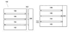
- This approachis illustrated, in overly simplified form, in FIG. 12 where the ICs that are bridged to each other 1202 , 1204 , 1210 , 1212 have a commonly aligned edge 1216 and in FIG. 13 where the ICs 1302 , 1306 , 1308 that are bridged to each other are offset from each other (i.e., their pertinent edges 1312 , 1314 , 1316 , 1318 are not commonly aligned).
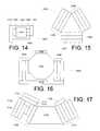
- FIGS. 14 through 17illustrate, in overly simplified form, some example modules 1400 , 1500 , 1600 , 1700 employing our approach and the kinds of complex configurations ICs made possible through use of our approach (with the understanding that these examples are purely representative and could never illustrate every possible permutation and combination).
- the connections between ICsinclude one or more of a post and penetration connection, a confined solder connection, a metal-to-metal fusion connection and/or a covalent bonding connection.
- a stack of four ICs 1402 , 1404 , 1406 , 1408are have an off plane IC 1410 connected to them on the left side and three of the ICs 1404 , 1406 , 1408 in the stack also have an off plane IC 1412 on their right side.
- a further IC 1414bridges the ICs 1402 , 1404 , 1406 , 1408 in the stack on the front side.
- a stack of multiple triangular ICs 1502each has a stack of three ICs 1504 , 1506 , 1508 on each of the three side faces of the stack 1502 .
- a more complex module 1600 arrangementhas a stack of multiple octagonal ICs 1602 (only one of which is visible in this view) having a stack of three ICs 1604 , 1606 on either side, a single IC 1608 on the upper face and a single IC 1610 on the lower face that also bridges the stacks on either side to each other.
- a stack of multiple trapezoidal ICs 1702(only one of which is visible in this view) have an off plane stack of ICs 1704 connected to it on the right side and that stack 1704 , in turn, has an off plane IC 1706 on its upper surface.
- the trapezoidal stack 1702has a stack 1708 of varying size ICs on its left side which, in turn has a two IC stack 1710 bridging the lower two ICs 1712 , 1714 to the upper two ICs 1716 , 1718 .
- any ICcan be an off plane IC with respect to a particular stack while also being part of a stack itself and even having an off plane IC connected to it or another one or more ICs in its stack.
- FIG. 18 and FIG. 19illustrate, in overly simplified form, how the approach described herein can be used with conventional passive elements such as an element configured with an RDL as well as interposers or flex circuitry.
- a module 1800is made up of complex stack of ICs and also includes a passive element 1802 , in this case flex circuitry, that interconnects a connection point 1804 between the middle two ICs 1806 , 1808 in the vertical stack with a connection point 1810 of the lower IC 1812 at the rightmost extreme of the module and partially wraps around a portion of the module.
- the passive elementis configured so that conventional ICs 1814 , 1816 , 1818 can be connected to it using conventional techniques, such as, for example, the ball grid arrays 1820 on the three chips located above the top of the passive element 1802 .
- a module 1900is made up of a stack of four vertically stacked ICs 1902 , 1904 , 1906 , 1908 .
- the module 1900includes a passive element 1910 , in this case an interposer that has rigid posts on one face so that it can form post and penetration interconnections with the stacked ICs 1902 , 1904 , 1906 , 1908 and conventional connections 1912 on its other face where a conventional IC 1914 is connected in a known manner.
- the passive elements 1802 , 1910 of FIG. 18 or of FIG. 19can optionally include, in the case of the passive element 1802 of FIG. 18 a rigid portion, or, in the case of the passive element 1910 of FIG. 19 , a flexible portion so that it can be supportive (in the case of the passive element 1802 of FIG. 18 ) or wrap around more than one side (in the case of the passive element 1910 of FIG. 19 ) and, optionally, form connections on faces of ICs in addition to on the side of a stack.
- the passive elementfor example the passive element 1802 of FIG. 18 could include a connection that joins to the stack, by way of example, at the connection point 1822 between the two upper and rightmost chips 1824 , 1826 or at another connection point between the two upper leftmost chips 1808 , 1830 .
Landscapes
- Engineering & Computer Science (AREA)
- Microelectronics & Electronic Packaging (AREA)
- Power Engineering (AREA)
- Computer Hardware Design (AREA)
- Physics & Mathematics (AREA)
- Condensed Matter Physics & Semiconductors (AREA)
- General Physics & Mathematics (AREA)
- Wire Bonding (AREA)
- Credit Cards Or The Like (AREA)
- Packaging Frangible Articles (AREA)
- Stackable Containers (AREA)
Abstract
Description
This application is a Continuation of U.S. patent application Ser. No. 11/688,088, filed Mar. 19, 2007, which is a Continuation-in-Part of the following patent applications which each claim priority to U.S. Provisional Patent Application No. 60/690,759 (filed Jun. 14, 2005): U.S. patent application Ser. Nos. 11/329,481, 11/329,506, 11/329,539, 11/329,540, 11/329,556, 11/329,557, 11/329,558 (now U.S. Pat. No. 7,560,813), Ser. No. 11/329,574 (now U.S. Pat. No. 7,534,722), Ser. Nos. 11/329,575, 11/329,576, 11/329,873 (now U.S. Pat. No. 7,538,033), Ser. Nos. 11/329,874, 11/329,875, 11/329,883, 11/329,885, 11/329,886 (now U.S. Pat. No. 7,521,806), Ser. No. 11/329,887 (now U.S. Pat. No. 7,215,032), Ser. Nos. 11/329,952, 11/329,953 (now U.S. Pat. No. 7,157,372), Ser. Nos. 11/329,955, 11/330,011 (each filed Jan. 10, 2006) and U.S. patent application Ser. No. 11/422,551 (filed Jun. 6, 2006). Each of the applications listed in this paragraph is incorporated herein by reference as if fully set forth herein.
The present invention relates to semiconductors and, more particularly, to stacking of device-bearing semiconductors.
For some time now, there has been a desire to increase the number of devices that can occupy a particular area on a circuit board in order to reduce the overall circuit board size. One of the ways that entities have approached doing so is by stacking packaged chips on top of one another. This is typically accomplished by use of an ancillary element, for example, a mini “circuit board” or “interposer” that two or more chips can connect to, or through use of flexible circuitry on a ribbon-like material that can wrap over or around one or more chips to affect the same result. These approaches connect to the chips from the top surfaces (i.e., at the points of connection) so the connecting material or interposer is parallel to the chips themselves. These two approaches achieve a smaller footprint, but do so at the expense of, for example added parasitic capacitance, noise or both. Moreover, such elements are always passive elements in that they cannot themselves include integrated circuit devices.
Thus, there is a need in the art for a better way of stacked packaging that does not require the use of such ancillary elements, is not restricted by the geometries and limited connectivity of the above approaches, or both.
We have devised a way of creating denser packages of stacked integrated circuits (“ICs”) (whether chips or dies) (hereafter “ICs”) that avoids the requirement of using purely passive ancillary elements like mini circuit boards, interposers or flexible circuits.
Advantageously, although the approaches herein avoid the above requirement, they are fully compatible with the techniques described above and thus provide benefits and advantages over and above such techniques, even where an ancillary element approach is used.
One aspect involves a module that has at least two ICs electrically and physically connected to each other such that they lie in different planes and are arranged as a first stack of ICs, a third IC electrically and physically connected to at least one of the at least two ICs, wherein the third IC is off plane from both of the at least two ICs, and at least one electrical connection exists between the third IC and the at least one of the at least two ICs. This electrical connection can be a post an penetration connection or some other form of connection.
The advantages and features described herein are a few of the many advantages and features available from representative embodiments and are presented only to assist in understanding the invention. It should be understood that they are not to be considered limitations on the invention as defined by the claims, or limitations on equivalents to the claims. For instance, some of these advantages are mutually contradictory, in that they cannot be simultaneously present in a single embodiment. Similarly, some advantages are applicable to one aspect of the invention, and inapplicable to others. Thus, this summary of features and advantages should not be considered dispositive in determining equivalence. Additional features and advantages of the invention will become apparent in the following description, from the drawings, and from the claims.
U.S. patent application Ser. Nos. 11,688,088, 11/329,481, 11/329,506, 11/329,539, 11/329,540, 11/329,556, 11/329,557, 11/329,558, 11/329,574, 11/329,575, 11/329,576, 11/329,873, 11/329,874, 11/329,875, 11/329,883, 11/329,885, 11/329,886, 11/329,887, 11/329,952, 11/329,953, 11/329,955, 11/330,011 and 11/422,551, incorporated herein by reference, describe various techniques for forming small, deep vias in, and electrical contacts for, semiconductor wafers. Our techniques allow for via densities and placement that was previously unachievable and can be performed on a chip, die or wafer scale. Moreover, our techniques allow for more flexible approaches stacking of chips to reduce the footprint occupied by chips relative to a simply coplanar arrangement of the same chips.
Specifically, our approach can leverage a solder connection or a post and penetration type connection as well as the various attachment approaches in the above-incorporated applications, like a well or reverse well approach, to facilitate attaching of one element to another element, irrespective of whether each is a chip, die, or passive element such as a re-direction layered (“RDL”) element or even an interposer or flexible circuitry on a ribbon-like material.
Moreover, our approach removes an orientation limit present in the conventional approach of vertically stacking chips in parallel planes. With our approach, the stacking can occur in substantially perpendicular as well as parallel planes.
The approach is described by way of a few examples wherein those examples generically illustrate a much broader scope due to the limitless number of variations that can be created.
Thecontacts 112 on the IC are then brought into contact forming the connection between theIC 200 and thestack 100. If post and penetration connections are used, then theconnections 112 would be posts which connect, under the appropriate pressure, with the correspondingmalleable contacts 302 thereby forming the post and penetration connection between theIC 200 and thestack 100, as shown inFIG. 4 .
Depending upon the particular implementation, the off plane element can, itself, be an integrated circuit bearing chip (or a portion thereof) or can be a passive element (whether rigid or flexible) or some other element, for example, a packaging element that contains RDLs but no circuitry. Thus, in the examples that follow, although the off plane pieces are described as ICs, it should be understood that the term “ICs” herein are not restricted to integrated circuits but could instead be (and are intended to encompass) any of the above passive elements as well.
At this point it should be appreciated that, with some implementations, the post and penetration connection can optionally be augmented by use of our tack and fuse process, which is described in detail in the above-incorporated U.S. patent applications. With this approach, a tack connection can be used to initially join the chips in a non-permanent connection. At some point thereafter, the chips can undergo a fuse process to make the connections “permanent.” In an alternative optional approach, a fuse process can be used without the tack process, although this will directly make the connections permanent.
Furthermore, with this off plane stacking approach, in some implementation situations, a reflowable material like a solder could be substituted for the malleable material if a barrier is used to confine the molten solder and prevent it from causing an undesirable short with another connection. Depending upon the implementation, this “barrier” approach can involve use of a well, such as described in the above-incorporated applications, or some other physical wall that is part of, applied to or formed on the IC. Alternatively, for example, if theconnection components
Based upon the foregoing, it should now be understood that this approach can occur on more than one side of a chip stack. Thus, it is possible to connect two or more perpendicular chips to a stack, thereby allowing for mixing of different speed technology chips and shortening connections between chips.
Depending upon the particular implementation, it should be understood that the formation of the stack of ICs can occur before, or concurrent with, the attachment of the perpendicular IC. Moreover, it should be understood that, while the above example located all of the malleable contacts in the stack of ICs and the rigid posts on the perpendicular IC for purposes of illustration and simplicity, different implementations can place the malleable or other type ofcontacts 302 on a perpendicular IC and theposts 112 on the mating ICs. Of course, still other implementations can have any one or more of the ICs each include a mixture of different contact types such as, for example,rigid posts 112 andmalleable contacts 302 such as shown in thestack 500 ofFIG. 5 .
Bearing the above in mind, additional aspects can advantageously be incorporated into the approach. For example, as shown inFIG. 6 , one or more of theICs module 600 can include afeature 612 that, depending upon the particular instance, can be formed on the IC or formed separately and attached to the IC. The particular feature can be formed through use of a known etching technique on the IC or formed separately from some other appropriate material, be it a plastic, ceramic, semiconductor, deposited metal or other material. The feature can thus serve as a spacer to maintain or define a minimum separation between the IC and some other IC, act as analignment element 614 itself or in a mating fashion with anotherfeature 616, or serve some other purpose for the particular application.
Alternatively and/or optionally, a “standoff” can be created directly under a malleable or solder contact to create a minimum and reproducible spacing between adjacent pieces in a stack or between an off plane IC and a stack.
At this point it should be mentioned that, although the above examples have used a single off plane IC, the off plane IC could equally be part of an IC stack itself As a result, it should be appreciated that chip modules can be formed in geometries that go far beyond simple vertical stacking. Moreover, because the above approach provides a way to bring connections closer together by allowing them to reside on different ICs than they otherwise would in a simple coplanar or vertically stacked arrangement, connections can be shortened, different speed ICs can be mixed, and problems like noise and parasitics can be addressed in entirely new ways. Still further, through use of the approach, ICs having shapes (in plan view) other than square or rectangular, such as those representative examples shown inFIG. 11A through 11H , for example, ICs of triangular, other quadrilateral, hexagonal, octagonal, or even irregular shapes can be used, the limiting factor now being the ability to dice those shapes from a wafer or otherwise saw, cut or create them.
Still further, it is to be understood that the off plane IC can be used to bridge ICs so as to provide a more direct connection between them while bypassing one or more ICs that are located in between them. This approach is illustrated, in overly simplified form, inFIG. 12 where the ICs that are bridged to each other1202,1204,1210,1212 have a commonly alignededge 1216 and inFIG. 13 where theICs pertinent edges
For example, as shown in the module1400FIG. 14 , a stack of fourICs off plane IC 1410 connected to them on the left side and three of theICs off plane IC 1412 on their right side. In addition, afurther IC 1414 bridges theICs
As shown in themodule 1500 ofFIG. 15 , a stack of multiple triangular ICs1502 (only one of which is visible in this view) each has a stack of threeICs stack 1502.
As shown inFIG. 16 , a morecomplex module 1600 arrangement has a stack of multiple octagonal ICs1602 (only one of which is visible in this view) having a stack of threeICs single IC 1608 on the upper face and asingle IC 1610 on the lower face that also bridges the stacks on either side to each other.
As shown in the module1700 ofFIG. 17 , a stack of multiple trapezoidal ICs1702 (only one of which is visible in this view) have an off plane stack ofICs 1704 connected to it on the right side and thatstack 1704, in turn, has anoff plane IC 1706 on its upper surface. In addition, thetrapezoidal stack 1702 has astack 1708 of varying size ICs on its left side which, in turn has a twoIC stack 1710 bridging the lower twoICs ICs
From the modules ofFIGS. 14 through 17 , it can be seen that any IC can be an off plane IC with respect to a particular stack while also being part of a stack itself and even having an off plane IC connected to it or another one or more ICs in its stack.
As shown inFIG. 18 , amodule 1800 is made up of complex stack of ICs and also includes apassive element 1802, in this case flex circuitry, that interconnects aconnection point 1804 between the middle twoICs connection point 1810 of thelower IC 1812 at the rightmost extreme of the module and partially wraps around a portion of the module. In addition, the passive element is configured so thatconventional ICs ball grid arrays 1820 on the three chips located above the top of thepassive element 1802.
As shown inFIG. 19 , amodule 1900 is made up of a stack of four vertically stackedICs module 1900 includes apassive element 1910, in this case an interposer that has rigid posts on one face so that it can form post and penetration interconnections with the stackedICs conventional connections 1912 on its other face where aconventional IC 1914 is connected in a known manner.
Finally, in some implementations, thepassive elements FIG. 18 or ofFIG. 19 can optionally include, in the case of thepassive element 1802 ofFIG. 18 a rigid portion, or, in the case of thepassive element 1910 ofFIG. 19 , a flexible portion so that it can be supportive (in the case of thepassive element 1802 ofFIG. 18 ) or wrap around more than one side (in the case of thepassive element 1910 ofFIG. 19 ) and, optionally, form connections on faces of ICs in addition to on the side of a stack. In such an implementation, the passive element, for example thepassive element 1802 ofFIG. 18 could include a connection that joins to the stack, by way of example, at theconnection point 1822 between the two upper andrightmost chips leftmost chips
It should thus be understood that this description (including the figures) is only representative of some illustrative embodiments. For the convenience of the reader, the above description has focused on a representative sample of all possible embodiments, a sample that teaches the principles of the invention. The description has not attempted to exhaustively enumerate all possible variations. That alternate embodiments may not have been presented for a specific portion of the invention, or that further undescribed alternate embodiments may be available for a portion, is not to be considered a disclaimer of those alternate embodiments. One of ordinary skill will appreciate that many of those undescribed embodiments incorporate the same principles of the invention and others are equivalent.
Claims (51)
1. A module comprising:
a first integrated circuit (IC) electrically connected to a second IC by a physical connection located between facing surfaces of the first and second ICs, wherein the facing surfaces of the first and second ICs extend along a first plane; and
a third IC electrically connected to the physical connection, wherein the third IC includes a facing surface from which an electrically-conductive element extends, wherein the electrically-conductive element is electrically and physically connected to the physical connection, and wherein the facing surface of the third IC lies in a second plane that is substantially perpendicular to the first plane.
2. The module ofclaim 1 , wherein the physical connection comprises a rigid post penetrated into a malleable material.
3. The module ofclaim 2 , wherein the electrically-conductive element comprises a rigid post, and wherein the third IC is electrically connected to the physical connection by the electrically-conductive element which extends from the third IC into the malleable material.
4. The module ofclaim 3 , wherein the third IC is located adjacent a first edge of the first IC and a first edge of the second IC that is offset from the first edge of the first IC such that the third IC is not exactly perpendicular to the first and second ICs, and wherein the length of the rigid post extending from the third IC is sufficient to compensate for the offset between the first edges of the first and second ICs.
5. The module ofclaim 1 , wherein the physical connection comprises a confined solder connection, a fusion connection, a well-type connection, or a covalent bond connection.
6. The module ofclaim 1 , wherein the third IC comprises a passive element electrically connecting at least one of the first or second ICs to a fourth IC.
7. The module ofclaim 6 , wherein the passive element comprises a flexible portion.
8. The module ofclaim 7 , wherein the passive element further comprises a rigid portion.
9. The module ofclaim 7 , wherein the passive element wraps around at least two sides of at least one of the first or second ICs.
10. The module ofclaim 1 , wherein the first IC comprises a first side surface and the second IC comprises a second side surface that is substantially aligned with the first side surface, and wherein the third IC comprises a facing surface that is substantially perpendicular to and adjacent to the first and second surfaces.
11. The module ofclaim 1 , wherein the third IC is one IC in a stack of additional ICs.
12. The module ofclaim 1 , further comprising a fourth IC electrically connected to the second IC and a fifth IC electrically connected to the fourth IC, wherein the third IC is substantially perpendicular to the fourth and fifth ICs, and wherein the third IC provides a bridge connection between the physical connection located between facing surfaces of the first and second ICs and another physical connection located between facing surfaces of the fourth and fifth ICs.
13. The module ofclaim 1 , further comprising a spacer disposed between the first and second ICs, wherein the spacer is configured to establish a minimum allowable spacing between the first and second ICs.
14. The module ofclaim 13 , wherein the spacer is part of one of the first or second ICs.
15. The module ofclaim 1 , further comprising a contact disposed between the first and second ICs, wherein the contact is configured to establish a minimum allowable spacing between the first and second ICs.
16. A module comprising:
a stack of integrated circuits (ICs) including a first IC that is electrically connected to a second IC by a physical connection located between facing surfaces of the first and second ICs; and
a third IC including a facing surface from which an electrically-conductive element extends, wherein the facing surface of the third IC is positioned along a lateral surface of the stack, and wherein the third IC is electrically connected by the electrically-conductive element to at least one of the first or second ICs at the physical connection located between the facing surfaces of the first and second ICs.
17. The module ofclaim 16 , wherein the third IC is substantially perpendicular to the first and second ICs.
18. The module ofclaim 16 , wherein the physical connection comprises a rigid post extending into a malleable material.
19. The module ofclaim 16 , wherein the physical connection comprises a confined solder connection, a fusion connection, a well-type connection, or a covalent bond connection.
20. The module ofclaim 16 , wherein the third IC comprises a passive element electrically connecting at least one of the first or second ICs to a fourth IC.
21. The module ofclaim 20 , wherein the passive element comprises a flexible portion and a rigid portion.
22. The module ofclaim 21 , wherein the passive element wraps around at least two sides of the stack of ICs.
23. The module ofclaim 16 , wherein the physical connection comprises a malleable material, and wherein the electrically-conductive element of the third IC extends into the malleable material.
24. The module ofclaim 16 , wherein the lateral surface of the stack comprises a commonly-aligned edge that includes a first side surface of the first IC and a second side surface of the second IC, and wherein the third IC comprises a facing surface that is substantially perpendicular to the commonly-aligned edge.
25. The module ofclaim 16 , wherein the stack of ICs further comprises a fourth IC electrically connected to the second IC and a fifth IC electrically connected to the fourth IC, and wherein the third IC provides a bridge connection between the physical connection located between the first and second ICs and a physical connection located between the fourth and fifth ICs.
26. The module ofclaim 16 , further comprising a spacer disposed between the first and second ICs, wherein the spacer is configured to establish a minimum spacing between the first and second ICs.
27. The module ofclaim 16 , wherein the first and second ICs are misaligned such that a first side surface of the first IC is not commonly-aligned with a second side surface of the second IC, and wherein the first and second side surfaces correspond to the lateral surface of the stack of ICs.
28. A module comprising:
a first integrated circuit (IC) electrically and physically coupled to both a second IC and a third IC at a common connection point, wherein the first IC includes a first element extending from a first facing surface, wherein the second IC includes a second element extending from a second facing surface, wherein the third IC includes a third element extending from a third facing surface, wherein the first, second, and third elements are electrically and physically connected at the common connection point, and wherein the third facing surface lies in a plane that is substantially perpendicular to a plane in which the first and second facing surfaces lie.
29. The module ofclaim 28 , wherein the first and second ICs are arranged in a facing relationship and the common connection point is between the first and second ICs.
30. The module ofclaim 28 , wherein the third IC is positioned adjacent lateral edges of the first and second ICs.
31. The module ofclaim 30 , wherein the lateral edges of the first and second ICs are not coplanar and the third IC is arranged at an angle other than 90 degrees with respect to the first and second ICs.
32. The module ofclaim 28 , wherein the common connection point comprises a malleable material and the first and third ICs each include at least one rigid post that penetrates into the malleable material.
33. The module ofclaim 28 , wherein the common connection point comprises a confined solder connection, a fusion connection, a well-type connection, or a covalent bond connection.
34. The module ofclaim 28 , wherein the third IC comprises a passive element electrically connecting at least one of the first or second ICs to a fourth IC.
35. A method comprising:
electrically connecting a first integrated circuit (IC) to a second IC via a physical connection located between facing surfaces of the first and second ICs, wherein the facing surfaces of the first and second ICs extend along a first plane; and
electrically connecting a third IC to the physical connection, wherein the third IC includes a facing surface from which an electrically-conductive element extends, wherein the electrically-conductive element is electrically and physically connected to the physical connection, and wherein the facing surface of the third IC lies in a second plane that is substantially perpendicular to the first plane.
36. The method ofclaim 35 , wherein said electrically connecting a third IC to the physical connection comprises inserting the electrically-conductive element into a malleable material.
37. The method ofclaim 36 , wherein the electrically-conductive element comprises a rigid post, and wherein the physical connection between facing surfaces of the first and second ICs comprises the malleable material.
38. The method ofclaim 35 , wherein said electrically connecting a third IC to the physical connection comprises one of a fusion process or a covalent bonding process.
39. The method ofclaim 35 , wherein said electrically connecting a third IC to the physical connection comprises a solder reflow process, and wherein reflowed solder is confined to a well.
40. The method ofclaim 35 , wherein said electrically connecting a third IC to the physical connection comprises electrically connecting at least one of the first or second ICs to a passive element of the third IC, the method further comprising electrically connecting the passive element to a fourth IC such that an electrical connection is formed between the fourth IC and at least one of the first or second ICs.
41. The method ofclaim 40 , wherein the passive element comprises a flexible portion and a rigid portion.
42. The method ofclaim 35 , wherein the first IC comprises a first side surface and the second IC comprises a second side surface that is substantially aligned with the first side surface, the method further comprising positioning the facing surface of the third IC substantially perpendicular to and adjacent to the first and second side surfaces.
43. The method ofclaim 35 , further comprising:
electrically connecting a fourth IC to the second IC;
electrically connecting a fifth IC to the fourth IC; and
providing an electrical bridge connection between the physical connection located between facing surfaces of the first and second ICs and another physical connection located between facing surfaces of the fourth and fifth ICs.
44. The method ofclaim 35 , further comprising providing a spacer between the first and second ICs, wherein the spacer is configured to establish a minimum allowable spacing between the first and second ICs.
45. The method ofclaim 44 , wherein the spacer is part of one of the first or second ICs.
46. The method ofclaim 35 , wherein a first side surface of the first IC is not commonly-aligned with a second side surface of the second IC such that the third IC is arranged at an angle other than 90 degrees with respect to the first and second ICs.
47. A method comprising:
electrically connecting a first integrated circuit (IC) to a second integrated circuit by a physical connection located between facing surfaces of the first and second ICs to form a stack of ICs;
positioning a third IC on a lateral surface of the stack of ICs, wherein the third IC includes a facing surface from which an electrically-conductive element extends; and
electrically connecting, via the electrically-conductive element, the third IC to at least one of the first or second ICs at the physical connection located between the facing surfaces of the first and second ICs.
48. The method ofclaim 47 , wherein said electrically connecting the third IC to at least one of the first or second ICs comprises inserting the electrically-conductive element of the third IC into a malleable material of the physical connection.
49. The method ofclaim 47 , wherein said electrically connecting the third IC to at least one of the first or second ICs comprises one of a fusion process, a covalent bonding process, or a solder reflow process.
50. The method ofclaim 47 , wherein the stack of ICs comprises a commonly-aligned edge that includes a first side surface of the first IC and a second side surface of the second IC, the method further comprising positioning the facing surface of the third IC substantially perpendicular to and adjacent to the commonly-aligned edge.
51. The method ofclaim 47 , further comprising:
electrically connecting a fourth IC to the second IC;
electrically connecting a fifth IC to the fourth IC, wherein the stack of ICs includes the fourth and fifth ICs; and
providing an electrical, bridge connection between the connection point located between the facing surfaces of the first and second ICs and another connection point located between facing surfaces of the fourth and fifth ICs.
Priority Applications (1)
| Application Number | Priority Date | Filing Date | Title |
|---|---|---|---|
| US12/710,811US8084851B2 (en) | 2005-06-14 | 2010-02-23 | Side stacking apparatus and method |
Applications Claiming Priority (25)
| Application Number | Priority Date | Filing Date | Title |
|---|---|---|---|
| US69075905P | 2005-06-14 | 2005-06-14 | |
| US11/329,557US7838997B2 (en) | 2005-06-14 | 2006-01-10 | Remote chip attachment |
| US11/329,576US7989958B2 (en) | 2005-06-14 | 2006-01-10 | Patterned contact |
| US11/329,574US7534722B2 (en) | 2005-06-14 | 2006-01-10 | Back-to-front via process |
| US11/329,506US7942182B2 (en) | 2005-06-14 | 2006-01-10 | Rigid-backed, membrane-based chip tooling |
| US11/329,539US20060278331A1 (en) | 2005-06-14 | 2006-01-10 | Membrane-based chip tooling |
| US11/329,955US20060278996A1 (en) | 2005-06-14 | 2006-01-10 | Active packaging |
| US11/329,556US7767493B2 (en) | 2005-06-14 | 2006-01-10 | Post & penetration interconnection |
| US11/329,874US20060278966A1 (en) | 2005-06-14 | 2006-01-10 | Contact-based encapsulation |
| US11/329,873US7538033B2 (en) | 2005-06-14 | 2006-01-10 | Post-attachment chip-to-chip connection |
| US11/329,481US8154131B2 (en) | 2005-06-14 | 2006-01-10 | Profiled contact |
| US11/329,885US7781886B2 (en) | 2005-06-14 | 2006-01-10 | Electronic chip contact structure |
| US11/329,953US7157372B1 (en) | 2005-06-14 | 2006-01-10 | Coaxial through chip connection |
| US11/329,887US7215032B2 (en) | 2005-06-14 | 2006-01-10 | Triaxial through-chip connection |
| US11/330,011US20060281303A1 (en) | 2005-06-14 | 2006-01-10 | Tack & fuse chip bonding |
| US11/329,952US7786592B2 (en) | 2005-06-14 | 2006-01-10 | Chip capacitive coupling |
| US11/329,540US7851348B2 (en) | 2005-06-14 | 2006-01-10 | Routingless chip architecture |
| US11/329,886US7521806B2 (en) | 2005-06-14 | 2006-01-10 | Chip spanning connection |
| US11/329,875US7969015B2 (en) | 2005-06-14 | 2006-01-10 | Inverse chip connector |
| US11/329,883US7946331B2 (en) | 2005-06-14 | 2006-01-10 | Pin-type chip tooling |
| US11/329,558US7560813B2 (en) | 2005-06-14 | 2006-01-10 | Chip-based thermo-stack |
| US11/329,575US7884483B2 (en) | 2005-06-14 | 2006-01-10 | Chip connector |
| US11/422,551US7847412B2 (en) | 2005-06-14 | 2006-06-06 | Isolating chip-to-chip contact |
| US11/688,088US7687400B2 (en) | 2005-06-14 | 2007-03-19 | Side stacking apparatus and method |
| US12/710,811US8084851B2 (en) | 2005-06-14 | 2010-02-23 | Side stacking apparatus and method |
Related Parent Applications (1)
| Application Number | Title | Priority Date | Filing Date |
|---|---|---|---|
| US11/688,088ContinuationUS7687400B2 (en) | 2005-06-14 | 2007-03-19 | Side stacking apparatus and method |
Publications (2)
| Publication Number | Publication Date |
|---|---|
| US20100148343A1 US20100148343A1 (en) | 2010-06-17 |
| US8084851B2true US8084851B2 (en) | 2011-12-27 |
Family
ID=39639338
Family Applications (2)
| Application Number | Title | Priority Date | Filing Date |
|---|---|---|---|
| US11/688,088ActiveUS7687400B2 (en) | 2005-06-14 | 2007-03-19 | Side stacking apparatus and method |
| US12/710,811ActiveUS8084851B2 (en) | 2005-06-14 | 2010-02-23 | Side stacking apparatus and method |
Family Applications Before (1)
| Application Number | Title | Priority Date | Filing Date |
|---|---|---|---|
| US11/688,088ActiveUS7687400B2 (en) | 2005-06-14 | 2007-03-19 | Side stacking apparatus and method |
Country Status (5)
| Country | Link |
|---|---|
| US (2) | US7687400B2 (en) |
| JP (1) | JP2011521437A (en) |
| KR (1) | KR20100137344A (en) |
| CN (1) | CN101689544A (en) |
| WO (1) | WO2008116230A2 (en) |
Cited By (1)
| Publication number | Priority date | Publication date | Assignee | Title |
|---|---|---|---|---|
| US11887908B2 (en) | 2021-12-21 | 2024-01-30 | International Business Machines Corporation | Electronic package structure with offset stacked chips and top and bottom side cooling lid |
Families Citing this family (25)
| Publication number | Priority date | Publication date | Assignee | Title |
|---|---|---|---|---|
| US7831151B2 (en) | 2001-06-29 | 2010-11-09 | John Trezza | Redundant optical device array |
| US7560813B2 (en) | 2005-06-14 | 2009-07-14 | John Trezza | Chip-based thermo-stack |
| US7989958B2 (en) | 2005-06-14 | 2011-08-02 | Cufer Assett Ltd. L.L.C. | Patterned contact |
| US7687400B2 (en) | 2005-06-14 | 2010-03-30 | John Trezza | Side stacking apparatus and method |
| US7786592B2 (en) | 2005-06-14 | 2010-08-31 | John Trezza | Chip capacitive coupling |
| US7851348B2 (en) | 2005-06-14 | 2010-12-14 | Abhay Misra | Routingless chip architecture |
| US8456015B2 (en) | 2005-06-14 | 2013-06-04 | Cufer Asset Ltd. L.L.C. | Triaxial through-chip connection |
| US7767493B2 (en) | 2005-06-14 | 2010-08-03 | John Trezza | Post & penetration interconnection |
| US7521806B2 (en) | 2005-06-14 | 2009-04-21 | John Trezza | Chip spanning connection |
| US7534722B2 (en) | 2005-06-14 | 2009-05-19 | John Trezza | Back-to-front via process |
| US7781886B2 (en) | 2005-06-14 | 2010-08-24 | John Trezza | Electronic chip contact structure |
| US7838997B2 (en) | 2005-06-14 | 2010-11-23 | John Trezza | Remote chip attachment |
| US7687397B2 (en) | 2006-06-06 | 2010-03-30 | John Trezza | Front-end processed wafer having through-chip connections |
| US7670874B2 (en) | 2007-02-16 | 2010-03-02 | John Trezza | Plated pillar package formation |
| WO2008137511A1 (en)* | 2007-05-04 | 2008-11-13 | Crossfire Technologies, Inc. | Accessing or interconnecting integrated circuits |
| US8476749B2 (en)* | 2009-07-22 | 2013-07-02 | Oracle America, Inc. | High-bandwidth ramp-stack chip package |
| US8290319B2 (en)* | 2010-08-25 | 2012-10-16 | Oracle America, Inc. | Optical communication in a ramp-stack chip package |
| US20120119345A1 (en)* | 2010-11-15 | 2012-05-17 | Cho Sungwon | Integrated circuit packaging system with device mount and method of manufacture thereof |
| US8587088B2 (en)* | 2011-02-17 | 2013-11-19 | Apple Inc. | Side-mounted controller and methods for making the same |
| US9082632B2 (en) | 2012-05-10 | 2015-07-14 | Oracle International Corporation | Ramp-stack chip package with variable chip spacing |
| DE112012006625B4 (en) | 2012-06-25 | 2023-09-28 | Intel Corporation | Multi-chip layer semiconductor structure with vertical intermediate side chip and semiconductor package therefor |
| US9252148B2 (en) | 2014-01-22 | 2016-02-02 | Micron Technology, Inc. | Methods and apparatuses with vertical strings of memory cells and support circuitry |
| CN107994011B (en)* | 2016-10-26 | 2020-06-02 | 晟碟信息科技(上海)有限公司 | Semiconductor package and method of manufacturing the same |
| MY192051A (en)* | 2016-12-29 | 2022-07-25 | Intel Corp | Stacked dice systems |
| CN112018097B (en)* | 2020-09-03 | 2022-09-23 | 长江存储科技有限责任公司 | Semiconductor structure and manufacturing method thereof |
Citations (278)
| Publication number | Priority date | Publication date | Assignee | Title |
|---|---|---|---|---|
| US3312878A (en) | 1965-06-01 | 1967-04-04 | Ibm | High speed packaging of miniaturized circuit modules |
| US3591839A (en) | 1969-08-27 | 1971-07-06 | Siliconix Inc | Micro-electronic circuit with novel hermetic sealing structure and method of manufacture |
| US3720309A (en) | 1971-12-07 | 1973-03-13 | Teledyne Inc | Method and apparatus for sorting semiconductor dice |
| US4200272A (en) | 1978-06-12 | 1980-04-29 | Bcira | Holder for irregularly shaped articles |
| US4452557A (en) | 1980-11-13 | 1984-06-05 | U.S. Philips Corporation | Device for the simultaneous positioning of a plurality of electrical and/or electronic parts on a printed circuit board |
| US4818728A (en) | 1986-12-03 | 1989-04-04 | Sharp Kabushiki Kaisha | Method of making a hybrid semiconductor device |
| US4873205A (en) | 1987-12-21 | 1989-10-10 | International Business Machines Corporation | Method for providing silicide bridge contact between silicon regions separated by a thin dielectric |
| US4878611A (en) | 1986-05-30 | 1989-11-07 | American Telephone And Telegraph Company, At&T Bell Laboratories | Process for controlling solder joint geometry when surface mounting a leadless integrated circuit package on a substrate |
| US4893174A (en) | 1985-07-08 | 1990-01-09 | Hitachi, Ltd. | High density integration of semiconductor circuit |
| US4915494A (en) | 1988-07-06 | 1990-04-10 | Harris Corporation | Carbon-carbon mirror for space applications |
| US4967248A (en) | 1987-04-15 | 1990-10-30 | Nec Corporation | Structure of semiconductor memory cell with trench-type capacitor |
| US4999077A (en) | 1989-08-31 | 1991-03-12 | Xerox Corporation | Method of fabricating full width scanning or imaging arrays from subunits |
| US5089055A (en) | 1989-12-12 | 1992-02-18 | Takashi Nakamura | Survivable solar power-generating systems for use with spacecraft |
| US5089880A (en) | 1989-06-07 | 1992-02-18 | Amdahl Corporation | Pressurized interconnection system for semiconductor chips |
| US5090119A (en) | 1987-12-08 | 1992-02-25 | Matsushita Electric Industrial Co., Ltd. | Method of forming an electrical contact bump |
| US5100480A (en) | 1990-04-18 | 1992-03-31 | Mitsubishi Denki Kabushiki Kaisha | Solar cell and method for manufacturing the same |
| US5120597A (en) | 1990-11-28 | 1992-06-09 | Teijin Limited | Press-cushion sheet |
| US5134460A (en) | 1986-08-11 | 1992-07-28 | International Business Machines Corporation | Aluminum bump, reworkable bump, and titanium nitride structure for tab bonding |
| EP0516866A1 (en) | 1991-05-03 | 1992-12-09 | International Business Machines Corporation | Modular multilayer interwiring structure |
| US5179043A (en) | 1989-07-14 | 1993-01-12 | The Texas A&M University System | Vapor deposited micro heat pipes |
| US5220530A (en) | 1990-08-07 | 1993-06-15 | Oki Electric Industry Co., Ltd. | Semiconductor memory element and method of fabricating the same |
| US5229315A (en) | 1991-01-16 | 1993-07-20 | Gold Star Electron Co., Ltd. | Method for forming an isolated film on a semiconductor device |
| US5234149A (en) | 1992-08-28 | 1993-08-10 | At&T Bell Laboratories | Debondable metallic bonding method |
| US5236854A (en) | 1989-12-11 | 1993-08-17 | Yukio Higaki | Compound semiconductor device and method for fabrication thereof |
| US5266912A (en) | 1992-08-19 | 1993-11-30 | Micron Technology, Inc. | Inherently impedance matched multiple integrated circuit module |
| US5308784A (en) | 1991-10-02 | 1994-05-03 | Samsung Electronics Co., Ltd. | Semiconductor device and method for making the same |
| US5399898A (en) | 1992-07-17 | 1995-03-21 | Lsi Logic Corporation | Multi-chip semiconductor arrangements using flip chip dies |
| US5427834A (en) | 1991-10-31 | 1995-06-27 | Idm Enterprises | Waterproof textile |
| US5468655A (en) | 1994-10-31 | 1995-11-21 | Motorola, Inc. | Method for forming a temporary attachment between a semiconductor die and a substrate using a metal paste comprising spherical modules |
| US5470787A (en) | 1994-05-02 | 1995-11-28 | Motorola, Inc. | Semiconductor device solder bump having intrinsic potential for forming an extended eutectic region and method for making and using the same |
| US5510655A (en) | 1990-11-26 | 1996-04-23 | The Boeing Company | Silicon wafers containing conductive feedthroughs |
| US5523628A (en) | 1994-08-05 | 1996-06-04 | Hughes Aircraft Company | Apparatus and method for protecting metal bumped integrated circuit chips during processing and for providing mechanical support to interconnected chips |
| US5561594A (en) | 1994-01-11 | 1996-10-01 | Sgs-Thomson Microelectronics Ltd. | Circuit connection in an electrical assembly |
| US5563084A (en) | 1994-09-22 | 1996-10-08 | Fraunhofer-Gesellschaft zur F orderung der angewandten Forschung e.V. | Method of making a three-dimensional integrated circuit |
| US5587119A (en) | 1994-09-14 | 1996-12-24 | E-Systems, Inc. | Method for manufacturing a coaxial interconnect |
| US5589029A (en) | 1994-07-21 | 1996-12-31 | Matsushita Electric Industrial Co., Ltd. | Semiconductor chip-supply method and apparatus |
| US5598965A (en) | 1994-11-03 | 1997-02-04 | Scheu; William E. | Integrated circuit, electronic component chip removal and replacement system |
| EP0757386A2 (en) | 1995-08-02 | 1997-02-05 | International Business Machines Corporation | Systems interconnected by bumps of joining material |
| US5608264A (en) | 1995-06-05 | 1997-03-04 | Harris Corporation | Surface mountable integrated circuit with conductive vias |
| US5635014A (en) | 1995-06-19 | 1997-06-03 | Gr Systems | Press apparatus and methods for fusing overlapped thermoplastic sheet materials |
| US5708569A (en) | 1993-04-07 | 1998-01-13 | Zycon Corporation | Annular circuit components coupled with printed circuit board through-hole |
| US5737186A (en) | 1995-04-20 | 1998-04-07 | Daimler-Benz Ag | Arrangement of plural micro-cooling devices with electronic components |
| US5773889A (en) | 1992-11-17 | 1998-06-30 | Fujitsu Limited | Wire interconnect structures for connecting an integrated circuit to a substrate |
| EP0620701B1 (en) | 1993-04-16 | 1998-07-08 | Kabushiki Kaisha Toshiba | Circuit devices and fabrication method of the same |
| US5780776A (en) | 1996-05-31 | 1998-07-14 | Nec Corporation | Multilayer circuit board unit |
| US5796591A (en) | 1995-06-07 | 1998-08-18 | International Business Machines Corporation | Direct chip attach circuit card |
| US5814889A (en) | 1995-06-05 | 1998-09-29 | Harris Corporation | Intergrated circuit with coaxial isolation and method |
| US5846464A (en) | 1997-03-28 | 1998-12-08 | Mcdonnell Douglas Corporation | Method for forming composite parts using reconfigurable modular tooling |
| US5872338A (en) | 1996-04-10 | 1999-02-16 | Prolinx Labs Corporation | Multilayer board having insulating isolation rings |
| US5874780A (en) | 1995-07-27 | 1999-02-23 | Nec Corporation | Method of mounting a semiconductor device to a substrate and a mounted structure |
| US5897337A (en) | 1994-09-30 | 1999-04-27 | Nec Corporation | Process for adhesively bonding a semiconductor chip to a carrier film |
| US5912510A (en) | 1996-05-29 | 1999-06-15 | Motorola, Inc. | Bonding structure for an electronic device |
| US5929524A (en) | 1995-12-14 | 1999-07-27 | Nec Corporation | Semiconductor device having ring-shaped conductive spacer which connects wiring layers |
| US5963793A (en) | 1996-05-29 | 1999-10-05 | Mcnc | Microelectronic packaging using arched solder columns |
| US5962922A (en) | 1998-03-18 | 1999-10-05 | Wang; Bily | Cavity grid array integrated circuit package |
| US5973396A (en) | 1996-02-16 | 1999-10-26 | Micron Technology, Inc. | Surface mount IC using silicon vias in an area array format or same size as die array |
| US6030894A (en) | 1996-12-04 | 2000-02-29 | Nec Corporation | Method for manufacturing a semiconductor device having contact plug made of Si/SiGe/Si |
| US6037665A (en) | 1997-03-03 | 2000-03-14 | Nec Corporation | Mounting assembly of integrated circuit device and method for production thereof |
| US6075710A (en) | 1998-02-11 | 2000-06-13 | Express Packaging Systems, Inc. | Low-cost surface-mount compatible land-grid array (LGA) chip scale package (CSP) for packaging solder-bumped flip chips |
| US6084301A (en) | 1995-02-13 | 2000-07-04 | Industrial Technology Industrial Research | Composite bump structures |
| US6087719A (en) | 1997-04-25 | 2000-07-11 | Kabushiki Kaisha Toshiba | Chip for multi-chip semiconductor device and method of manufacturing the same |
| US6118181A (en) | 1998-07-29 | 2000-09-12 | Agilent Technologies, Inc. | System and method for bonding wafers |
| US6133631A (en) | 1997-05-30 | 2000-10-17 | Hewlett-Packard Company | Semiconductor package lid with internal heat pipe |
| US6135635A (en) | 1999-10-07 | 2000-10-24 | Miller; Jeffrey | Convertible bag and barrier device |
| US6137184A (en) | 1997-04-28 | 2000-10-24 | Nec Corporation | Flip-chip type semiconductor device having recessed-protruded electrodes in press-fit contact |
| US6135054A (en) | 1997-09-10 | 2000-10-24 | Nippon Pillar Packing Co. Ltd. | Semiconductor wafer holder with CVD silicon carbide film coating |
| US6184066B1 (en) | 1997-05-28 | 2001-02-06 | Matsushita Electric Industrial Co., Ltd. | Method for fabricating semiconductor device |
| US6188118B1 (en) | 1996-08-06 | 2001-02-13 | Nortel Networks Limited | Semiconductor photodetector packaging |
| US6207475B1 (en) | 1999-03-30 | 2001-03-27 | Industrial Technology Research Institute | Method for dispensing underfill and devices formed |
| US6215114B1 (en) | 1997-09-25 | 2001-04-10 | Canon Kk | Optical probe for detecting or irradiating light and near-field optical microscope having such probe and manufacturing method of such probe |
| US6232668B1 (en) | 1999-02-02 | 2001-05-15 | Rohm Co. Ltd. | Semiconductor device of chip-on-chip structure and semiconductor chip for use therein |
| US20010001292A1 (en) | 1998-04-07 | 2001-05-17 | Bertin Claude Louis | Through-chip conductors for low inductance chip-to-chip integration and off-chip connections |
| US6277711B1 (en) | 2001-01-08 | 2001-08-21 | Jiahn-Chang Wu | Semiconductor matrix formation |
| US6283693B1 (en) | 1999-11-12 | 2001-09-04 | General Semiconductor, Inc. | Method and apparatus for semiconductor chip handling |
| US6297072B1 (en) | 1998-04-17 | 2001-10-02 | Interuniversitair Micro-Elktronica Centrum (Imec Vzw) | Method of fabrication of a microstructure having an internal cavity |
| US6314013B1 (en) | 1998-11-23 | 2001-11-06 | Micron Technology, Inc. | Stacked integrated circuits |
| US6316737B1 (en) | 1999-09-09 | 2001-11-13 | Vlt Corporation | Making a connection between a component and a circuit board |
| US6316786B1 (en) | 1998-08-29 | 2001-11-13 | International Business Machines Corporation | Organic opto-electronic devices |
| US6326115B1 (en) | 1997-10-31 | 2001-12-04 | Sanyo Chemical Industries, Ltd. | Toner and toner binder |
| US6335571B1 (en) | 1997-07-21 | 2002-01-01 | Miguel Albert Capote | Semiconductor flip-chip package and method for the fabrication thereof |
| US20020004299A1 (en) | 1994-08-15 | 2002-01-10 | Schuele Paul J. | Method of fabricating a contract structure having a composite barrier layer between a platinium layer and a polysilicon plug |
| US20020019099A1 (en) | 1999-04-22 | 2002-02-14 | Richard K. Williams | Super self-aligned trench-gate dmos with reduced on-resistance |
| US6351384B1 (en) | 1999-08-11 | 2002-02-26 | Hitachi, Ltd. | Device and method for cooling multi-chip modules |
| US20020048847A1 (en) | 1997-01-09 | 2002-04-25 | Kazuhisa Tsunoi | Method of mounting semiconductor chip part on substrate |
| US6393638B1 (en) | 1999-04-20 | 2002-05-28 | Maccoll Ian Coats | Waterproof blanket with integrated storage bag |
| US6395633B1 (en) | 2001-05-16 | 2002-05-28 | World Wiser Electrics Inc. | Method of forming micro-via |
| US6399426B1 (en) | 1998-07-21 | 2002-06-04 | Miguel Albert Capote | Semiconductor flip-chip package and method for the fabrication thereof |
| US6410415B1 (en) | 1999-03-23 | 2002-06-25 | Polymer Flip Chip Corporation | Flip chip mounting technique |
| US20020081773A1 (en) | 1997-01-31 | 2002-06-27 | Tomio Inoue | Light-emitting element, semiconductor light-emitting device, and manufacturing methods therefor |
| US6429045B1 (en) | 2001-02-07 | 2002-08-06 | International Business Machines Corporation | Structure and process for multi-chip chip attach with reduced risk of electrostatic discharge damage |
| US20020104873A1 (en) | 2001-02-06 | 2002-08-08 | Lee Michael G. | Multilayer interconnection and method |
| US20020109236A1 (en) | 2001-02-09 | 2002-08-15 | Samsung Electronics Co., Ltd. | Three-dimensional multi-chip package having chip selection pads and manufacturing method thereof |
| US6451626B1 (en) | 2001-07-27 | 2002-09-17 | Charles W.C. Lin | Three-dimensional stacked semiconductor package |
| US6484776B1 (en) | 2000-04-07 | 2002-11-26 | Northrop Grumman Corporation | System for constructing a laminate |
| US6492255B2 (en) | 1998-09-30 | 2002-12-10 | Ibiden Co., Ltd | Semiconductor chip and method manufacturing the same |
| US6498503B2 (en) | 1996-04-01 | 2002-12-24 | Micron Technology, Inc. | Semiconductor test interconnect with variable flexure contacts |
| US6498089B2 (en) | 2001-03-09 | 2002-12-24 | Fujitsu Limited | Semiconductor integrated circuit device with moisture-proof ring and its manufacture method |
| US6501185B1 (en) | 2001-06-12 | 2002-12-31 | Advanced Interconnect Technology Ltd. | Barrier cap for under bump metal |
| US6503779B2 (en) | 2000-05-26 | 2003-01-07 | Nec Corporation | Method of manufacturing flip chip type semiconductor device |
| US6509256B2 (en) | 1998-02-12 | 2003-01-21 | Micron Technology, Inc. | Methods of forming electrically conductive interconnections and electrically interconnected substrates |
| US6513236B2 (en) | 2000-02-18 | 2003-02-04 | Matsushita Electric Industrial Co., Ltd. | Method of manufacturing bump-component mounted body and device for manufacturing the same |
| US20030030367A1 (en) | 1997-03-31 | 2003-02-13 | Canon Kabushiki Kaisha | Image forming apparatus and method of manufacturing the same |
| US6531022B1 (en) | 1996-06-07 | 2003-03-11 | Matsushita Electric Industrial Co., Ltd. | Mounting method of semiconductor element |
| US6544371B2 (en) | 1999-06-07 | 2003-04-08 | Lintec Corporation | Method of using a transfer tape |
| US6551858B2 (en) | 1998-06-01 | 2003-04-22 | Hitachi, Ltd. | Method of producing a semiconductor device having two semiconductor chips sealed by a resin |
| US6555418B2 (en) | 1995-12-05 | 2003-04-29 | Kabushiki Kaisha Toshiba | Method for separating a semiconductor element in a semiconductor element pushing-up device |
| US6557192B2 (en) | 2001-01-02 | 2003-05-06 | Patent Category Corp. | Sleeping bag with enhancements |
| US6559540B2 (en) | 2000-02-09 | 2003-05-06 | Nec Electronics Corporation | Flip-chip semiconductor device and method of forming the same |
| US20030085471A1 (en) | 2001-11-07 | 2003-05-08 | Takahiro Iijima | Semiconductor package and method of production thereof |
| US20030094700A1 (en) | 2001-11-16 | 2003-05-22 | Fujitsu Limited | Light signal processing system |
| US6576830B2 (en) | 1998-12-04 | 2003-06-10 | Canon Kabushiki Kaisha | Solar cell roof structure, construction method thereof, photovoltaic power generating apparatus, and building |
| US6577013B1 (en) | 2000-09-05 | 2003-06-10 | Amkor Technology, Inc. | Chip size semiconductor packages with stacked dies |
| US6583517B1 (en) | 2002-04-09 | 2003-06-24 | International Business Machines Corporation | Method and structure for joining two substrates with a low melt solder joint |
| US6586090B2 (en) | 2000-02-24 | 2003-07-01 | Nitto Denko Corporation | Adhesive tape and substrate for adhesive tape |
| US6590278B1 (en) | 2002-01-08 | 2003-07-08 | International Business Machines Corporation | Electronic package |
| US6596640B1 (en) | 2002-06-21 | 2003-07-22 | Intel Corporation | Method of forming a raised contact for a substrate |
| US6599778B2 (en) | 2001-12-19 | 2003-07-29 | International Business Machines Corporation | Chip and wafer integration process using vertical connections |
| US20030145939A1 (en) | 2002-02-06 | 2003-08-07 | Ahn Seung Chul | Dual die bonder for a semiconductor device and a method thereof |
| US6611057B2 (en) | 2000-11-09 | 2003-08-26 | Nec Corporation | Semiconductor device attaining both high speed processing and sufficient cooling capacity |
| US6617507B2 (en) | 2001-11-16 | 2003-09-09 | First Solar, Llc | Photovoltaic array |
| US6617688B2 (en) | 2001-03-27 | 2003-09-09 | Nec Electronics Corporation | Semiconductor device and flat electrodes |
| US6627477B1 (en) | 2000-09-07 | 2003-09-30 | International Business Machines Corporation | Method of assembling a plurality of semiconductor devices having different thickness |
| US20030183947A1 (en) | 2002-04-01 | 2003-10-02 | Nec Electronics Corporation | Flip-chip type semiconductor device, process for manufacturing such semiconductor device, and process for mounting such semiconductor device |
| US6633079B2 (en) | 2001-01-10 | 2003-10-14 | Raytheon Company | Wafer level interconnection |
| US20030193076A1 (en) | 2002-04-11 | 2003-10-16 | Robert Patti | Interlocking conductor method for bonding wafers to produce stacked integrated circuits |
| US6635960B2 (en) | 2001-08-30 | 2003-10-21 | Micron Technology, Inc. | Angled edge connections for multichip structures |
| US6635970B2 (en) | 2002-02-06 | 2003-10-21 | International Business Machines Corporation | Power distribution design method for stacked flip-chip packages |
| US20030206680A1 (en) | 2002-05-03 | 2003-11-06 | Georgia Tech Research Corporation | Devices having compliant wafer-level input/output interconnections and packages using pillars and methods of fabrication thereof |
| US6649941B2 (en) | 1998-12-22 | 2003-11-18 | Toyoda Gosei Co., Ltd. | Method for manufacturing semiconductor device using group III nitride compound |
| US20030216030A1 (en) | 2002-05-18 | 2003-11-20 | Hai-Won Kim | Method for fabricating contact plug with low contact resistance |
| US20030214036A1 (en) | 2002-05-14 | 2003-11-20 | Motorola Inc. | Under bump metallurgy structural design for high reliability bumped packages |
| US20030222354A1 (en) | 2002-04-05 | 2003-12-04 | Stmicroelectronics S.R.I. | Process for manufacturing a through insulated interconnection in a body of semiconductor material |
| US6674647B2 (en) | 2002-01-07 | 2004-01-06 | International Business Machines Corporation | Low or no-force bump flattening structure and method |
| US6680540B2 (en) | 2000-03-08 | 2004-01-20 | Hitachi, Ltd. | Semiconductor device having cobalt alloy film with boron |
| US6686654B2 (en) | 2001-08-31 | 2004-02-03 | Micron Technology, Inc. | Multiple chip stack structure and cooling system |
| US6689949B2 (en) | 2002-05-17 | 2004-02-10 | United Innovations, Inc. | Concentrating photovoltaic cavity converters for extreme solar-to-electric conversion efficiencies |
| US6689627B2 (en) | 2000-12-20 | 2004-02-10 | Stmicroelectronics S.R.L. | Process for manufacturing micromechanical components in a semiconductor material wafer with reduction in the starting wafer thickness |
| US20040029304A1 (en) | 2002-03-27 | 2004-02-12 | Intel Corporation | Packaging of multiple active optical devices |
| US20040031973A1 (en) | 2002-05-27 | 2004-02-19 | Stmicroelectronics S.R.I | Process for manufacturing encapsulated optical sensors, and an encapsulated optical sensor manufactured using this process |
| US20040041260A1 (en) | 2002-08-29 | 2004-03-04 | Wood Alan G. | Semiconductor component with backside contacts and method of fabrication |
| US6703555B2 (en) | 2001-05-31 | 2004-03-09 | Canon Kabushiki Kaisha | Solar cell string, solar cell array and solar photovoltaic power system |
| US6706554B2 (en) | 2000-10-26 | 2004-03-16 | Oki Electric Industry Co., Ltd. | Conductor posts, construction for and method of fabricating semiconductor integrated circuit chips using the conductor post, and method of probing semiconductor integrated circuit chips |
| US6704953B2 (en) | 2002-06-05 | 2004-03-16 | Zelma Lee Fishman | Combination sleeping bag and mat for infants and children |
| US6717071B2 (en) | 2000-08-11 | 2004-04-06 | Industrial Technology Research Institute | Coaxial via hole and process of fabricating the same |
| US6717045B2 (en) | 2001-10-23 | 2004-04-06 | Leon L. C. Chen | Photovoltaic array module design for solar electric power generation systems |
| US6720245B2 (en) | 2000-09-07 | 2004-04-13 | Interuniversitair Microelektronica Centrum (Imec) | Method of fabrication and device for electromagnetic-shielding structures in a damascene-based interconnect scheme |
| US6727582B2 (en) | 2001-09-28 | 2004-04-27 | Rohm Co., Ltd. | Semiconductor device |
| US6731003B2 (en) | 2002-03-12 | 2004-05-04 | Fairchild Semiconductor Corporation | Wafer-level coated copper stud bumps |
| US6730840B2 (en) | 2001-03-23 | 2004-05-04 | Canon Kabushiki Kaisha | Concentrating photovoltaic module and concentrating photovoltaic power generating system |
| US6733685B2 (en) | 1996-09-20 | 2004-05-11 | Fujitsu Limited | Methods of planarizing structures on wafers and substrates by polishing |
| US6740576B1 (en) | 2000-10-13 | 2004-05-25 | Bridge Semiconductor Corporation | Method of making a contact terminal with a plated metal peripheral sidewall portion for a semiconductor chip assembly |
| US20040104791A1 (en) | 2002-08-13 | 2004-06-03 | Yoshio Satoh | Acoustic wave device and method of producing the same |
| US6756680B2 (en) | 1999-05-10 | 2004-06-29 | International Business Machines Corporation | Flip chip C4 extension structure and process |
| US6756594B2 (en) | 2000-01-28 | 2004-06-29 | California Institute Of Technology | Micromachined tuned-band hot bolometer emitter |
| US6765287B1 (en) | 2001-07-27 | 2004-07-20 | Charles W. C. Lin | Three-dimensional stacked semiconductor package |
| US6768210B2 (en) | 2001-11-01 | 2004-07-27 | Texas Instruments Incorporated | Bumpless wafer scale device and board assembly |
| US6770555B2 (en) | 1998-02-13 | 2004-08-03 | Nec Corporation | Process for fabricating semiconductor integrated circuit device having polycide line and impurity region respectively exposed to contact holes different in depth |
| US6770509B2 (en) | 2001-06-14 | 2004-08-03 | Ask S.A. | Method for connecting a chip to an antenna in a contactless smart card radio frequency identification device |
| US6770822B2 (en) | 2002-02-22 | 2004-08-03 | Bridgewave Communications, Inc. | High frequency device packages and methods |
| US6780280B2 (en) | 2001-09-27 | 2004-08-24 | Thomas Josef Heimbach Gesellschaft Mit Beschrankter Haftung & Co. | Pressing cushion |
| US20040169275A1 (en) | 2003-02-27 | 2004-09-02 | Motorola, Inc. | Area-array device assembly with pre-applied underfill layers on printed wiring board |
| US6790663B2 (en) | 1998-09-02 | 2004-09-14 | Micron Technology, Inc. | Methods of contacting lines and methods of forming an electrical contact in a semiconductor device |
| US20040177774A1 (en) | 2003-03-12 | 2004-09-16 | Sharp Kabushiki Kaisha | Reinforcement combining apparatus and method of combining reinforcement |
| US6798030B1 (en) | 1998-12-14 | 2004-09-28 | Sharp Kabushiki Kaisha | Two-dimensional image detecting device and manufacturing method thereof |
| US20040192029A1 (en) | 2001-10-18 | 2004-09-30 | Hartwell Peter George | Systems and methods for electrically isolating portions of wafers |
| US20040199998A1 (en) | 2002-11-19 | 2004-10-14 | Worlds Apart Limited | Convertible blanket |
| US6809020B2 (en) | 2000-05-01 | 2004-10-26 | Seiko Epson Corporation | Method for forming bump, semiconductor device and method for making the same, circuit board, and electronic device |
| US6815252B2 (en) | 2000-03-10 | 2004-11-09 | Chippac, Inc. | Method of forming flip chip interconnection structure |
| US6818818B2 (en) | 2002-08-13 | 2004-11-16 | Esmond T. Goei | Concentrating solar energy receiver |
| US20040227256A1 (en) | 2003-05-16 | 2004-11-18 | Sharp Kabushiki Kaisha | Semiconductor device and production method therefor |
| US6824643B2 (en) | 2001-10-23 | 2004-11-30 | Fujitsu Limited | Method and device of peeling semiconductor device using annular contact members |
| US20040238115A1 (en) | 2001-09-12 | 2004-12-02 | Hisao Matsuno | Circuit device mounting method and press |
| US6841883B1 (en) | 2003-03-31 | 2005-01-11 | Micron Technology, Inc. | Multi-dice chip scale semiconductor components and wafer level methods of fabrication |
| US6844259B2 (en) | 2002-03-30 | 2005-01-18 | Hynix Semiconductor Inc. | Method for forming contact plug in semiconductor device |
| US6846725B2 (en) | 2002-10-17 | 2005-01-25 | Institute Of Microelectronics | Wafer-level package for micro-electro-mechanical systems |
| US20050042838A1 (en) | 2002-03-01 | 2005-02-24 | Garyainov Stanislav A | Fluxless assembly of chip size semiconductor packages |
| US6861336B1 (en) | 2003-11-30 | 2005-03-01 | Union Semiconductor Technology Corporation | Die thinning methods |
| US20050048766A1 (en) | 2003-08-31 | 2005-03-03 | Wen-Chieh Wu | Method for fabricating a conductive plug in integrated circuit |
| US20050046034A1 (en) | 2003-09-03 | 2005-03-03 | Micron Technology, Inc. | Apparatus and method for high density multi-chip structures |
| US6869856B2 (en) | 2001-10-30 | 2005-03-22 | Stmicroelectronics S.R.L. | Process for manufacturing a semiconductor wafer integrating electronic devices including a structure for electromagnetic decoupling |
| US6872635B2 (en) | 2001-04-11 | 2005-03-29 | Sony Corporation | Device transferring method, and device arraying method and image display unit fabricating method using the same |
| US6881609B2 (en) | 2001-09-07 | 2005-04-19 | Peter C. Salmon | Component connections using bumps and wells |
| US6889427B2 (en) | 2002-02-15 | 2005-05-10 | Freescale Semiconductor, Inc. | Process for disengaging semiconductor die from an adhesive film |
| US20050104027A1 (en) | 2003-10-17 | 2005-05-19 | Lazarev Pavel I. | Three-dimensional integrated circuit with integrated heat sinks |
| US20050104219A1 (en) | 2003-09-26 | 2005-05-19 | Kuniyasu Matsui | Intermediate chip module, semiconductor device, circuit board, and electronic device |
| US6903443B2 (en) | 1997-12-18 | 2005-06-07 | Micron Technology, Inc. | Semiconductor component and interconnect having conductive members and contacts on opposing sides |
| US6909180B2 (en) | 2000-05-12 | 2005-06-21 | Matsushita Electric Industrial Co., Ltd. | Semiconductor device, mounting circuit board, method of producing the same, and method of producing mounting structure using the same |
| US6919642B2 (en) | 2002-07-05 | 2005-07-19 | Industrial Technology Research Institute | Method for bonding IC chips to substrates incorporating dummy bumps and non-conductive adhesive and structures formed |
| US6920051B2 (en) | 2000-03-31 | 2005-07-19 | Intel Corporation | Hybrid capacitor, circuit, and system |
| US20050167830A1 (en) | 2004-01-30 | 2005-08-04 | Phoenix Precision Technology Corporation | Pre-solder structure on semiconductor package substrate and method for fabricating the same |
| US6929974B2 (en) | 2002-10-18 | 2005-08-16 | Motorola, Inc. | Feedthrough design and method for a hermetically sealed microdevice |
| US20050184377A1 (en) | 2004-01-30 | 2005-08-25 | Shinko Electric Industries Co., Ltd. | Semiconductor device and method of manufacturing the same |
| US6938783B2 (en) | 2000-07-26 | 2005-09-06 | Amerasia International Technology, Inc. | Carrier tape |
| US6939789B2 (en) | 2002-05-13 | 2005-09-06 | Taiwan Semiconductor Manufacturing Co., Ltd. | Method of wafer level chip scale packaging |
| US20050230804A1 (en) | 2004-03-24 | 2005-10-20 | Kazumasa Tanida | Manufacturing method for semiconductor device, semiconductor device and semiconductor chip |
| US20050233504A1 (en) | 2003-03-06 | 2005-10-20 | Masato Doi | Device transfer method and display apparatus |
| US20050245059A1 (en) | 2004-04-30 | 2005-11-03 | Yuan Yuan | Method for making an interconnect pad |
| US6967307B2 (en) | 1998-09-02 | 2005-11-22 | Micron Technology, Inc. | Method and process of contact to a heat softened solder ball array |
| US20050258526A1 (en) | 2002-05-20 | 2005-11-24 | Takashi Noguchi | Semiconductor device, method for mounting the same, and method for repairing the same |
| US20050266670A1 (en) | 2004-05-05 | 2005-12-01 | Mou-Shiung Lin | Chip bonding process |
| US20050263869A1 (en) | 2004-05-25 | 2005-12-01 | Renesas Technology Corp. | Semiconductor device and manufacturing process therefor |
| US20050262634A1 (en) | 2004-05-28 | 2005-12-01 | Gottlieb Patricia R | Combination convertible blanket and pillow |
| US6975027B2 (en) | 2001-08-30 | 2005-12-13 | Micron Technology, Inc. | Multi-chip electronic package and cooling system |
| US20060001174A1 (en) | 2004-06-30 | 2006-01-05 | Nec Electronics Corporation | Semiconductor device and method for manufacturing the same |
| US6986377B2 (en) | 2002-09-30 | 2006-01-17 | Illinois Tool Works Inc. | Method and apparatus for guiding and sealing split-flange zipper tape to bag making film |
| US6992824B1 (en) | 2003-12-27 | 2006-01-31 | Motamedi Manouchehr E | Efficient wave propagation for terahertz imaging and sensing |
| US6995469B2 (en) | 2003-05-21 | 2006-02-07 | Olympus Corporation | Semiconductor apparatus and fabricating method for the same |
| US20060046468A1 (en) | 2004-08-31 | 2006-03-02 | Salman Akram | Through-substrate interconnect fabrication methods and resulting structures and assemblies |
| US7015590B2 (en) | 2003-01-10 | 2006-03-21 | Samsung Electronics Co., Ltd. | Reinforced solder bump structure and method for forming a reinforced solder bump |
| US7013509B2 (en) | 2003-03-28 | 2006-03-21 | Hickman Robert J | Easy on/easy off pillow and blanket cover |
| US7023347B2 (en) | 2002-08-02 | 2006-04-04 | Symbol Technologies, Inc. | Method and system for forming a die frame and for transferring dies therewith |
| US20060070704A1 (en) | 2004-10-06 | 2006-04-06 | Tropicana Products, Inc. | Vaccum support and transfer of flexible material |
| US20060073701A1 (en) | 2004-10-01 | 2006-04-06 | Shinko Electric Industries Co., Ltd | Method of manufacturing a substrate with through electrodes |
| US7052941B2 (en) | 2003-06-24 | 2006-05-30 | Sang-Yun Lee | Method for making a three-dimensional integrated circuit structure |
| US7053456B2 (en) | 2004-03-31 | 2006-05-30 | Kabushiki Kaisha Toshiba | Electronic component having micro-electrical mechanical system |
| US7056813B2 (en) | 2003-09-17 | 2006-06-06 | Intel Corporation | Methods of forming backside connections on a wafer stack |
| US7061104B2 (en) | 2002-02-07 | 2006-06-13 | Cooligy, Inc. | Apparatus for conditioning power and managing thermal energy in an electronic device |
| US20060128061A1 (en) | 2004-10-04 | 2006-06-15 | Ravi Kramadhati V | Fabrication of stacked die and structures formed thereby |
| US20060125084A1 (en) | 2004-12-15 | 2006-06-15 | Fazzio Ronald S | Integration of micro-electro mechanical systems and active circuitry |
| US20060170089A1 (en) | 2005-01-31 | 2006-08-03 | Fujitsu Limited | Electronic device and method for fabricating the same |
| US7107666B2 (en) | 1998-07-23 | 2006-09-19 | Bh Electronics | Method of manufacturing an ultra-miniature magnetic device |
| US20060208326A1 (en) | 2005-03-18 | 2006-09-21 | Nasiri Steven S | Method of fabrication of ai/ge bonding in a wafer packaging environment and a product produced therefrom |
| US7115984B2 (en) | 2002-06-18 | 2006-10-03 | Micron Technology, Inc. | Semiconductor devices including peripherally located bond pads, intermediates thereof, assemblies, and packages including the semiconductor devices, and support elements for the semiconductor devices |
| US20060223301A1 (en) | 2004-12-17 | 2006-10-05 | Serge Vanhaelemeersch | Formation of deep via airgaps for three dimensional wafer to wafer interconnect |
| US20060252262A1 (en) | 2005-05-03 | 2006-11-09 | Rockwell Scientific Licensing, Llc | Semiconductor structures having via structures between planar frontside and backside surfaces and methods of fabricating the same |
| US7138706B2 (en) | 2002-06-25 | 2006-11-21 | Matsushita Electric Industrial Co., Ltd. | Semiconductor device and method for manufacturing the same |
| US20060264029A1 (en) | 2005-05-23 | 2006-11-23 | Intel Corporation | Low inductance via structures |
| US7141869B2 (en) | 2004-11-08 | 2006-11-28 | Optopac, Inc. | Electronic package for image sensor, and the packaging method thereof |
| US7145236B2 (en) | 2000-06-12 | 2006-12-05 | Renesas Technology Corp. | Semiconductor device having solder bumps reliably reflow solderable |
| US7144759B1 (en) | 2004-04-02 | 2006-12-05 | Celerity Research Pte. Ltd. | Technology partitioning for advanced flip-chip packaging |
| US20060275946A1 (en) | 2005-05-04 | 2006-12-07 | Icemos Technology Corporation | Silicon Wafer Having Through-Wafer Vias |
| US20060278992A1 (en) | 2005-06-14 | 2006-12-14 | John Trezza | Post & penetration interconnection |
| US20060278988A1 (en) | 2005-06-14 | 2006-12-14 | John Trezza | Profiled contact |
| US20060281303A1 (en) | 2005-06-14 | 2006-12-14 | John Trezza | Tack & fuse chip bonding |
| US20060281363A1 (en) | 2005-06-14 | 2006-12-14 | John Trezza | Remote chip attachment |
| US20060292824A1 (en) | 2005-06-08 | 2006-12-28 | Eric Beyne | Methods for bonding and micro-electronic devices produced according to such methods |
| US7157310B2 (en) | 2004-09-01 | 2007-01-02 | Micron Technology, Inc. | Methods for packaging microfeature devices and microfeature devices formed by such methods |
| US20070020926A1 (en) | 2003-03-21 | 2007-01-25 | Edvard Kalvesten | Electrical connections in substrates |
| US7170183B1 (en) | 2005-05-13 | 2007-01-30 | Amkor Technology, Inc. | Wafer level stacked package |
| US7218349B2 (en) | 2001-08-09 | 2007-05-15 | Semiconductor Energy Laboratory Co., Ltd. | Semiconductor device |
| US7230318B2 (en) | 2003-12-24 | 2007-06-12 | Agency For Science, Technology And Research | RF and MMIC stackable micro-modules |
| US7233028B2 (en) | 2001-02-23 | 2007-06-19 | Nitronex Corporation | Gallium nitride material devices and methods of forming the same |
| US7242099B2 (en) | 2001-03-05 | 2007-07-10 | Megica Corporation | Chip package with multiple chips connected by bumps |
| US7249992B2 (en) | 2004-07-02 | 2007-07-31 | Strasbaugh | Method, apparatus and system for use in processing wafers |
| US7253519B2 (en) | 2003-06-09 | 2007-08-07 | Advanced Semiconductor Engineering, Inc. | Chip packaging structure having redistribution layer with recess |
| US20070184653A1 (en) | 2004-03-02 | 2007-08-09 | Pierre Blanchard | Integrated circuit with a very small-sized reading diode |
| US7262082B1 (en) | 2000-10-13 | 2007-08-28 | Bridge Semiconductor Corporation | Method of making a three-dimensional stacked semiconductor package with a metal pillar and a conductive interconnect in an encapsulant aperture |
| US7264984B2 (en) | 2004-12-21 | 2007-09-04 | Touchdown Technologies, Inc. | Process for forming MEMS |
| US7271491B1 (en) | 2000-08-31 | 2007-09-18 | Micron Technology, Inc. | Carrier for wafer-scale package and wafer-scale package including the carrier |
| US7276787B2 (en) | 2003-12-05 | 2007-10-02 | International Business Machines Corporation | Silicon chip carrier with conductive through-vias and method for fabricating same |
| US7294531B2 (en) | 2004-01-09 | 2007-11-13 | Samsung Electronics Co., Ltd. | Wafer level chip stack method |
| US7300857B2 (en) | 2004-09-02 | 2007-11-27 | Micron Technology, Inc. | Through-wafer interconnects for photoimager and memory wafers |
| US7303976B2 (en) | 2005-05-10 | 2007-12-04 | Hewlett-Packard Development Company, L.P. | Wafer bonding method |
| US20070278641A1 (en) | 2005-06-14 | 2007-12-06 | John Trezza | Side Stacking Apparatus and Method |
| US20080003817A1 (en) | 2004-05-25 | 2008-01-03 | Canon Kabushiki Kaisha | Method of manufacturing semiconductor device and semiconductor device |
| US20080017407A1 (en) | 2006-07-24 | 2008-01-24 | Ibiden Co., Ltd. | Interposer and electronic device using the same |
| US7326629B2 (en) | 2004-09-10 | 2008-02-05 | Agency For Science, Technology And Research | Method of stacking thin substrates by transfer bonding |
| US7371676B2 (en) | 2005-04-08 | 2008-05-13 | Micron Technology, Inc. | Method for fabricating semiconductor components with through wire interconnects |
| US20080111582A1 (en) | 2003-04-21 | 2008-05-15 | Elpida Memory, Inc. | Memory module and memory device |
| US20080116567A1 (en) | 2006-11-22 | 2008-05-22 | Ahmed Amin | Flip Chip Assembly Having Improved Thermal Dissipation |
| US7384863B2 (en) | 2000-07-17 | 2008-06-10 | Rohm Co., Ltd. | Semiconductor device and method for manufacturing the same |
| US7390735B2 (en) | 2005-01-07 | 2008-06-24 | Teledyne Licensing, Llc | High temperature, stable SiC device interconnects and packages having low thermal resistance |
| US7399652B2 (en) | 2003-04-08 | 2008-07-15 | Stmicroelectronics S.R.L. | Method for manufacturing a micro-electro-mechanical device, in particular an optical microswitch, and micro-electro-mechanical device thus obtained |
| US20080203556A1 (en) | 2005-05-18 | 2008-08-28 | Kolo Technologies, Inc. | Through-Wafer Interconnection |
| US20080213941A1 (en) | 2003-11-10 | 2008-09-04 | Pendse Rajendra D | Bump-on-Lead Flip Chip Interconnection |
| US20080254618A1 (en) | 2004-09-29 | 2008-10-16 | Sanyo Electric Co., Ltd. | Method of manufacturing a semiconductor device |
| US7456089B2 (en) | 2004-05-12 | 2008-11-25 | Fujitsu Limited | Semiconductor device and method of manufacturing the semiconductor device |
| US7456497B2 (en) | 2002-12-27 | 2008-11-25 | Shinko Electric Industries Co., Ltd. | Electronic devices and its production methods |
| US7488680B2 (en) | 2005-08-30 | 2009-02-10 | International Business Machines Corporation | Conductive through via process for electronic device carriers |
| US7495316B2 (en) | 2004-08-31 | 2009-02-24 | Micron Technology, Inc. | Methods of forming conductive vias and methods of forming multichip modules including such conductive vias |
| US7528494B2 (en) | 2005-11-03 | 2009-05-05 | International Business Machines Corporation | Accessible chip stack and process of manufacturing thereof |
| US7534722B2 (en) | 2005-06-14 | 2009-05-19 | John Trezza | Back-to-front via process |
| US20090149033A1 (en) | 2003-04-29 | 2009-06-11 | Micron Technology, Inc. | Systems and methods for forming metal oxide layers |
| US20090181497A1 (en) | 2004-08-05 | 2009-07-16 | Fujitsu Limited | Method for processing a base |
| US20090215976A1 (en) | 2004-07-07 | 2009-08-27 | Promerus Llc | Photosensitive dielectric resin compositions, films formed therefrom and semiconductor and display devices encompassing such films |
| US20090267165A1 (en) | 2005-11-25 | 2009-10-29 | Takafumi Okudo | Wafer level package structure, and sensor device obtained from the same package structure |
| US20090322698A1 (en) | 1999-07-06 | 2009-12-31 | Semiconductor Energy Laboratory Co., Ltd. | Semiconductor device and method of fabricating the same |
| US20100117236A1 (en) | 1998-12-21 | 2010-05-13 | Megica Corporation | Top layers of metal for high performance ic's |
Family Cites Families (2)
| Publication number | Priority date | Publication date | Assignee | Title |
|---|---|---|---|---|
| JP3056723B1 (en)* | 1999-01-04 | 2000-06-26 | ファナック株式会社 | Laser processing equipment |
| US20080284037A1 (en) | 2007-05-15 | 2008-11-20 | Andry Paul S | Apparatus and Methods for Constructing Semiconductor Chip Packages with Silicon Space Transformer Carriers |
- 2007
- 2007-03-19USUS11/688,088patent/US7687400B2/enactiveActive
- 2008
- 2008-05-19JPJP2009554797Apatent/JP2011521437A/enactivePending
- 2008-05-19CNCN200880009023Apatent/CN101689544A/enactivePending
- 2008-05-19KRKR1020097021563Apatent/KR20100137344A/ennot_activeWithdrawn
- 2008-05-19WOPCT/US2008/064136patent/WO2008116230A2/enactiveApplication Filing
- 2010
- 2010-02-23USUS12/710,811patent/US8084851B2/enactiveActive
Patent Citations (297)
| Publication number | Priority date | Publication date | Assignee | Title |
|---|---|---|---|---|
| US3312878A (en) | 1965-06-01 | 1967-04-04 | Ibm | High speed packaging of miniaturized circuit modules |
| US3591839A (en) | 1969-08-27 | 1971-07-06 | Siliconix Inc | Micro-electronic circuit with novel hermetic sealing structure and method of manufacture |
| US3720309A (en) | 1971-12-07 | 1973-03-13 | Teledyne Inc | Method and apparatus for sorting semiconductor dice |
| US4200272A (en) | 1978-06-12 | 1980-04-29 | Bcira | Holder for irregularly shaped articles |
| US4452557A (en) | 1980-11-13 | 1984-06-05 | U.S. Philips Corporation | Device for the simultaneous positioning of a plurality of electrical and/or electronic parts on a printed circuit board |
| US4893174A (en) | 1985-07-08 | 1990-01-09 | Hitachi, Ltd. | High density integration of semiconductor circuit |
| US4878611A (en) | 1986-05-30 | 1989-11-07 | American Telephone And Telegraph Company, At&T Bell Laboratories | Process for controlling solder joint geometry when surface mounting a leadless integrated circuit package on a substrate |
| US5134460A (en) | 1986-08-11 | 1992-07-28 | International Business Machines Corporation | Aluminum bump, reworkable bump, and titanium nitride structure for tab bonding |
| US4818728A (en) | 1986-12-03 | 1989-04-04 | Sharp Kabushiki Kaisha | Method of making a hybrid semiconductor device |
| US4967248A (en) | 1987-04-15 | 1990-10-30 | Nec Corporation | Structure of semiconductor memory cell with trench-type capacitor |
| US5090119A (en) | 1987-12-08 | 1992-02-25 | Matsushita Electric Industrial Co., Ltd. | Method of forming an electrical contact bump |
| US4873205A (en) | 1987-12-21 | 1989-10-10 | International Business Machines Corporation | Method for providing silicide bridge contact between silicon regions separated by a thin dielectric |
| US4915494A (en) | 1988-07-06 | 1990-04-10 | Harris Corporation | Carbon-carbon mirror for space applications |
| US5089880A (en) | 1989-06-07 | 1992-02-18 | Amdahl Corporation | Pressurized interconnection system for semiconductor chips |
| US5179043A (en) | 1989-07-14 | 1993-01-12 | The Texas A&M University System | Vapor deposited micro heat pipes |
| US4999077A (en) | 1989-08-31 | 1991-03-12 | Xerox Corporation | Method of fabricating full width scanning or imaging arrays from subunits |
| US5236854A (en) | 1989-12-11 | 1993-08-17 | Yukio Higaki | Compound semiconductor device and method for fabrication thereof |
| US5089055A (en) | 1989-12-12 | 1992-02-18 | Takashi Nakamura | Survivable solar power-generating systems for use with spacecraft |
| US5100480A (en) | 1990-04-18 | 1992-03-31 | Mitsubishi Denki Kabushiki Kaisha | Solar cell and method for manufacturing the same |
| US5220530A (en) | 1990-08-07 | 1993-06-15 | Oki Electric Industry Co., Ltd. | Semiconductor memory element and method of fabricating the same |
| US5510655A (en) | 1990-11-26 | 1996-04-23 | The Boeing Company | Silicon wafers containing conductive feedthroughs |
| US5120597A (en) | 1990-11-28 | 1992-06-09 | Teijin Limited | Press-cushion sheet |
| US5229315A (en) | 1991-01-16 | 1993-07-20 | Gold Star Electron Co., Ltd. | Method for forming an isolated film on a semiconductor device |
| EP0516866A1 (en) | 1991-05-03 | 1992-12-09 | International Business Machines Corporation | Modular multilayer interwiring structure |
| US5308784A (en) | 1991-10-02 | 1994-05-03 | Samsung Electronics Co., Ltd. | Semiconductor device and method for making the same |
| US5427834A (en) | 1991-10-31 | 1995-06-27 | Idm Enterprises | Waterproof textile |
| US5399898A (en) | 1992-07-17 | 1995-03-21 | Lsi Logic Corporation | Multi-chip semiconductor arrangements using flip chip dies |
| US5266912A (en) | 1992-08-19 | 1993-11-30 | Micron Technology, Inc. | Inherently impedance matched multiple integrated circuit module |
| US5234149A (en) | 1992-08-28 | 1993-08-10 | At&T Bell Laboratories | Debondable metallic bonding method |
| US5773889A (en) | 1992-11-17 | 1998-06-30 | Fujitsu Limited | Wire interconnect structures for connecting an integrated circuit to a substrate |
| US5708569A (en) | 1993-04-07 | 1998-01-13 | Zycon Corporation | Annular circuit components coupled with printed circuit board through-hole |
| EP0620701B1 (en) | 1993-04-16 | 1998-07-08 | Kabushiki Kaisha Toshiba | Circuit devices and fabrication method of the same |
| US5561594A (en) | 1994-01-11 | 1996-10-01 | Sgs-Thomson Microelectronics Ltd. | Circuit connection in an electrical assembly |
| US5470787A (en) | 1994-05-02 | 1995-11-28 | Motorola, Inc. | Semiconductor device solder bump having intrinsic potential for forming an extended eutectic region and method for making and using the same |
| US5589029A (en) | 1994-07-21 | 1996-12-31 | Matsushita Electric Industrial Co., Ltd. | Semiconductor chip-supply method and apparatus |
| US5523628A (en) | 1994-08-05 | 1996-06-04 | Hughes Aircraft Company | Apparatus and method for protecting metal bumped integrated circuit chips during processing and for providing mechanical support to interconnected chips |
| US20020004299A1 (en) | 1994-08-15 | 2002-01-10 | Schuele Paul J. | Method of fabricating a contract structure having a composite barrier layer between a platinium layer and a polysilicon plug |
| US5587119A (en) | 1994-09-14 | 1996-12-24 | E-Systems, Inc. | Method for manufacturing a coaxial interconnect |
| US5563084A (en) | 1994-09-22 | 1996-10-08 | Fraunhofer-Gesellschaft zur F orderung der angewandten Forschung e.V. | Method of making a three-dimensional integrated circuit |
| US5897337A (en) | 1994-09-30 | 1999-04-27 | Nec Corporation | Process for adhesively bonding a semiconductor chip to a carrier film |
| US5468655A (en) | 1994-10-31 | 1995-11-21 | Motorola, Inc. | Method for forming a temporary attachment between a semiconductor die and a substrate using a metal paste comprising spherical modules |
| US5598965A (en) | 1994-11-03 | 1997-02-04 | Scheu; William E. | Integrated circuit, electronic component chip removal and replacement system |
| US6084301A (en) | 1995-02-13 | 2000-07-04 | Industrial Technology Industrial Research | Composite bump structures |
| US5737186A (en) | 1995-04-20 | 1998-04-07 | Daimler-Benz Ag | Arrangement of plural micro-cooling devices with electronic components |
| US5608264A (en) | 1995-06-05 | 1997-03-04 | Harris Corporation | Surface mountable integrated circuit with conductive vias |
| US5814889A (en) | 1995-06-05 | 1998-09-29 | Harris Corporation | Intergrated circuit with coaxial isolation and method |
| US5796591A (en) | 1995-06-07 | 1998-08-18 | International Business Machines Corporation | Direct chip attach circuit card |
| US5635014A (en) | 1995-06-19 | 1997-06-03 | Gr Systems | Press apparatus and methods for fusing overlapped thermoplastic sheet materials |
| US5874780A (en) | 1995-07-27 | 1999-02-23 | Nec Corporation | Method of mounting a semiconductor device to a substrate and a mounted structure |
| EP0757386A2 (en) | 1995-08-02 | 1997-02-05 | International Business Machines Corporation | Systems interconnected by bumps of joining material |
| US6555418B2 (en) | 1995-12-05 | 2003-04-29 | Kabushiki Kaisha Toshiba | Method for separating a semiconductor element in a semiconductor element pushing-up device |
| US5929524A (en) | 1995-12-14 | 1999-07-27 | Nec Corporation | Semiconductor device having ring-shaped conductive spacer which connects wiring layers |
| US5973396A (en) | 1996-02-16 | 1999-10-26 | Micron Technology, Inc. | Surface mount IC using silicon vias in an area array format or same size as die array |
| US6498503B2 (en) | 1996-04-01 | 2002-12-24 | Micron Technology, Inc. | Semiconductor test interconnect with variable flexure contacts |
| US5872338A (en) | 1996-04-10 | 1999-02-16 | Prolinx Labs Corporation | Multilayer board having insulating isolation rings |
| US5963793A (en) | 1996-05-29 | 1999-10-05 | Mcnc | Microelectronic packaging using arched solder columns |
| US5912510A (en) | 1996-05-29 | 1999-06-15 | Motorola, Inc. | Bonding structure for an electronic device |
| US5780776A (en) | 1996-05-31 | 1998-07-14 | Nec Corporation | Multilayer circuit board unit |
| US6531022B1 (en) | 1996-06-07 | 2003-03-11 | Matsushita Electric Industrial Co., Ltd. | Mounting method of semiconductor element |
| US6188118B1 (en) | 1996-08-06 | 2001-02-13 | Nortel Networks Limited | Semiconductor photodetector packaging |
| US6733685B2 (en) | 1996-09-20 | 2004-05-11 | Fujitsu Limited | Methods of planarizing structures on wafers and substrates by polishing |
| US6030894A (en) | 1996-12-04 | 2000-02-29 | Nec Corporation | Method for manufacturing a semiconductor device having contact plug made of Si/SiGe/Si |
| US20020048847A1 (en) | 1997-01-09 | 2002-04-25 | Kazuhisa Tsunoi | Method of mounting semiconductor chip part on substrate |
| US20020081773A1 (en) | 1997-01-31 | 2002-06-27 | Tomio Inoue | Light-emitting element, semiconductor light-emitting device, and manufacturing methods therefor |
| US6037665A (en) | 1997-03-03 | 2000-03-14 | Nec Corporation | Mounting assembly of integrated circuit device and method for production thereof |
| US5846464A (en) | 1997-03-28 | 1998-12-08 | Mcdonnell Douglas Corporation | Method for forming composite parts using reconfigurable modular tooling |
| US20030030367A1 (en) | 1997-03-31 | 2003-02-13 | Canon Kabushiki Kaisha | Image forming apparatus and method of manufacturing the same |
| US6087719A (en) | 1997-04-25 | 2000-07-11 | Kabushiki Kaisha Toshiba | Chip for multi-chip semiconductor device and method of manufacturing the same |
| US6137184A (en) | 1997-04-28 | 2000-10-24 | Nec Corporation | Flip-chip type semiconductor device having recessed-protruded electrodes in press-fit contact |
| US6184066B1 (en) | 1997-05-28 | 2001-02-06 | Matsushita Electric Industrial Co., Ltd. | Method for fabricating semiconductor device |
| US6133631A (en) | 1997-05-30 | 2000-10-17 | Hewlett-Packard Company | Semiconductor package lid with internal heat pipe |
| US6335571B1 (en) | 1997-07-21 | 2002-01-01 | Miguel Albert Capote | Semiconductor flip-chip package and method for the fabrication thereof |
| US6135054A (en) | 1997-09-10 | 2000-10-24 | Nippon Pillar Packing Co. Ltd. | Semiconductor wafer holder with CVD silicon carbide film coating |
| US6215114B1 (en) | 1997-09-25 | 2001-04-10 | Canon Kk | Optical probe for detecting or irradiating light and near-field optical microscope having such probe and manufacturing method of such probe |
| US6326115B1 (en) | 1997-10-31 | 2001-12-04 | Sanyo Chemical Industries, Ltd. | Toner and toner binder |
| US6903443B2 (en) | 1997-12-18 | 2005-06-07 | Micron Technology, Inc. | Semiconductor component and interconnect having conductive members and contacts on opposing sides |
| US6075710A (en) | 1998-02-11 | 2000-06-13 | Express Packaging Systems, Inc. | Low-cost surface-mount compatible land-grid array (LGA) chip scale package (CSP) for packaging solder-bumped flip chips |
| US6509256B2 (en) | 1998-02-12 | 2003-01-21 | Micron Technology, Inc. | Methods of forming electrically conductive interconnections and electrically interconnected substrates |
| US6770555B2 (en) | 1998-02-13 | 2004-08-03 | Nec Corporation | Process for fabricating semiconductor integrated circuit device having polycide line and impurity region respectively exposed to contact holes different in depth |
| US5962922A (en) | 1998-03-18 | 1999-10-05 | Wang; Bily | Cavity grid array integrated circuit package |
| US20010001292A1 (en) | 1998-04-07 | 2001-05-17 | Bertin Claude Louis | Through-chip conductors for low inductance chip-to-chip integration and off-chip connections |
| US6410431B2 (en) | 1998-04-07 | 2002-06-25 | International Business Machines Corporation | Through-chip conductors for low inductance chip-to-chip integration and off-chip connections |
| US6297072B1 (en) | 1998-04-17 | 2001-10-02 | Interuniversitair Micro-Elktronica Centrum (Imec Vzw) | Method of fabrication of a microstructure having an internal cavity |
| US6551858B2 (en) | 1998-06-01 | 2003-04-22 | Hitachi, Ltd. | Method of producing a semiconductor device having two semiconductor chips sealed by a resin |
| US6399426B1 (en) | 1998-07-21 | 2002-06-04 | Miguel Albert Capote | Semiconductor flip-chip package and method for the fabrication thereof |
| US7107666B2 (en) | 1998-07-23 | 2006-09-19 | Bh Electronics | Method of manufacturing an ultra-miniature magnetic device |
| US6118181A (en) | 1998-07-29 | 2000-09-12 | Agilent Technologies, Inc. | System and method for bonding wafers |
| US6316786B1 (en) | 1998-08-29 | 2001-11-13 | International Business Machines Corporation | Organic opto-electronic devices |
| US6790663B2 (en) | 1998-09-02 | 2004-09-14 | Micron Technology, Inc. | Methods of contacting lines and methods of forming an electrical contact in a semiconductor device |
| US6967307B2 (en) | 1998-09-02 | 2005-11-22 | Micron Technology, Inc. | Method and process of contact to a heat softened solder ball array |
| US6492255B2 (en) | 1998-09-30 | 2002-12-10 | Ibiden Co., Ltd | Semiconductor chip and method manufacturing the same |
| US6395630B2 (en) | 1998-11-23 | 2002-05-28 | Micron Technology, Inc. | Stacked integrated circuits |
| US6314013B1 (en) | 1998-11-23 | 2001-11-06 | Micron Technology, Inc. | Stacked integrated circuits |
| US6576830B2 (en) | 1998-12-04 | 2003-06-10 | Canon Kabushiki Kaisha | Solar cell roof structure, construction method thereof, photovoltaic power generating apparatus, and building |
| US6798030B1 (en) | 1998-12-14 | 2004-09-28 | Sharp Kabushiki Kaisha | Two-dimensional image detecting device and manufacturing method thereof |
| US20100117236A1 (en) | 1998-12-21 | 2010-05-13 | Megica Corporation | Top layers of metal for high performance ic's |
| US6649941B2 (en) | 1998-12-22 | 2003-11-18 | Toyoda Gosei Co., Ltd. | Method for manufacturing semiconductor device using group III nitride compound |
| US6232668B1 (en) | 1999-02-02 | 2001-05-15 | Rohm Co. Ltd. | Semiconductor device of chip-on-chip structure and semiconductor chip for use therein |
| US6410415B1 (en) | 1999-03-23 | 2002-06-25 | Polymer Flip Chip Corporation | Flip chip mounting technique |
| US6207475B1 (en) | 1999-03-30 | 2001-03-27 | Industrial Technology Research Institute | Method for dispensing underfill and devices formed |
| US6393638B1 (en) | 1999-04-20 | 2002-05-28 | Maccoll Ian Coats | Waterproof blanket with integrated storage bag |
| US20020019099A1 (en) | 1999-04-22 | 2002-02-14 | Richard K. Williams | Super self-aligned trench-gate dmos with reduced on-resistance |
| US6756680B2 (en) | 1999-05-10 | 2004-06-29 | International Business Machines Corporation | Flip chip C4 extension structure and process |
| US6544371B2 (en) | 1999-06-07 | 2003-04-08 | Lintec Corporation | Method of using a transfer tape |
| US20090322698A1 (en) | 1999-07-06 | 2009-12-31 | Semiconductor Energy Laboratory Co., Ltd. | Semiconductor device and method of fabricating the same |
| US6351384B1 (en) | 1999-08-11 | 2002-02-26 | Hitachi, Ltd. | Device and method for cooling multi-chip modules |
| US6316737B1 (en) | 1999-09-09 | 2001-11-13 | Vlt Corporation | Making a connection between a component and a circuit board |
| US6135635A (en) | 1999-10-07 | 2000-10-24 | Miller; Jeffrey | Convertible bag and barrier device |
| US6283693B1 (en) | 1999-11-12 | 2001-09-04 | General Semiconductor, Inc. | Method and apparatus for semiconductor chip handling |
| US6756594B2 (en) | 2000-01-28 | 2004-06-29 | California Institute Of Technology | Micromachined tuned-band hot bolometer emitter |
| US6559540B2 (en) | 2000-02-09 | 2003-05-06 | Nec Electronics Corporation | Flip-chip semiconductor device and method of forming the same |
| US6513236B2 (en) | 2000-02-18 | 2003-02-04 | Matsushita Electric Industrial Co., Ltd. | Method of manufacturing bump-component mounted body and device for manufacturing the same |
| US6586090B2 (en) | 2000-02-24 | 2003-07-01 | Nitto Denko Corporation | Adhesive tape and substrate for adhesive tape |
| US6680540B2 (en) | 2000-03-08 | 2004-01-20 | Hitachi, Ltd. | Semiconductor device having cobalt alloy film with boron |
| US6815252B2 (en) | 2000-03-10 | 2004-11-09 | Chippac, Inc. | Method of forming flip chip interconnection structure |
| US7033859B2 (en) | 2000-03-10 | 2006-04-25 | Chippac, Inc. | Flip chip interconnection structure |
| US6920051B2 (en) | 2000-03-31 | 2005-07-19 | Intel Corporation | Hybrid capacitor, circuit, and system |
| US6484776B1 (en) | 2000-04-07 | 2002-11-26 | Northrop Grumman Corporation | System for constructing a laminate |
| US6809020B2 (en) | 2000-05-01 | 2004-10-26 | Seiko Epson Corporation | Method for forming bump, semiconductor device and method for making the same, circuit board, and electronic device |
| US6909180B2 (en) | 2000-05-12 | 2005-06-21 | Matsushita Electric Industrial Co., Ltd. | Semiconductor device, mounting circuit board, method of producing the same, and method of producing mounting structure using the same |
| US20050163982A1 (en) | 2000-05-12 | 2005-07-28 | Masahiro Ono | Circuit substrate for packaging semiconductor device, method for producing the same, and method for producing semiconductor device package structure using the same |
| US6503779B2 (en) | 2000-05-26 | 2003-01-07 | Nec Corporation | Method of manufacturing flip chip type semiconductor device |
| US7145236B2 (en) | 2000-06-12 | 2006-12-05 | Renesas Technology Corp. | Semiconductor device having solder bumps reliably reflow solderable |
| US7384863B2 (en) | 2000-07-17 | 2008-06-10 | Rohm Co., Ltd. | Semiconductor device and method for manufacturing the same |
| US6938783B2 (en) | 2000-07-26 | 2005-09-06 | Amerasia International Technology, Inc. | Carrier tape |
| US6717071B2 (en) | 2000-08-11 | 2004-04-06 | Industrial Technology Research Institute | Coaxial via hole and process of fabricating the same |
| US7271491B1 (en) | 2000-08-31 | 2007-09-18 | Micron Technology, Inc. | Carrier for wafer-scale package and wafer-scale package including the carrier |
| US6577013B1 (en) | 2000-09-05 | 2003-06-10 | Amkor Technology, Inc. | Chip size semiconductor packages with stacked dies |
| US6720245B2 (en) | 2000-09-07 | 2004-04-13 | Interuniversitair Microelektronica Centrum (Imec) | Method of fabrication and device for electromagnetic-shielding structures in a damascene-based interconnect scheme |
| US6627477B1 (en) | 2000-09-07 | 2003-09-30 | International Business Machines Corporation | Method of assembling a plurality of semiconductor devices having different thickness |
| US6740576B1 (en) | 2000-10-13 | 2004-05-25 | Bridge Semiconductor Corporation | Method of making a contact terminal with a plated metal peripheral sidewall portion for a semiconductor chip assembly |
| US7262082B1 (en) | 2000-10-13 | 2007-08-28 | Bridge Semiconductor Corporation | Method of making a three-dimensional stacked semiconductor package with a metal pillar and a conductive interconnect in an encapsulant aperture |
| US6706554B2 (en) | 2000-10-26 | 2004-03-16 | Oki Electric Industry Co., Ltd. | Conductor posts, construction for and method of fabricating semiconductor integrated circuit chips using the conductor post, and method of probing semiconductor integrated circuit chips |
| US6611057B2 (en) | 2000-11-09 | 2003-08-26 | Nec Corporation | Semiconductor device attaining both high speed processing and sufficient cooling capacity |
| US6689627B2 (en) | 2000-12-20 | 2004-02-10 | Stmicroelectronics S.R.L. | Process for manufacturing micromechanical components in a semiconductor material wafer with reduction in the starting wafer thickness |
| US6557192B2 (en) | 2001-01-02 | 2003-05-06 | Patent Category Corp. | Sleeping bag with enhancements |
| US6277711B1 (en) | 2001-01-08 | 2001-08-21 | Jiahn-Chang Wu | Semiconductor matrix formation |
| US6633079B2 (en) | 2001-01-10 | 2003-10-14 | Raytheon Company | Wafer level interconnection |
| US20020104873A1 (en) | 2001-02-06 | 2002-08-08 | Lee Michael G. | Multilayer interconnection and method |
| US6429045B1 (en) | 2001-02-07 | 2002-08-06 | International Business Machines Corporation | Structure and process for multi-chip chip attach with reduced risk of electrostatic discharge damage |
| US20020109236A1 (en) | 2001-02-09 | 2002-08-15 | Samsung Electronics Co., Ltd. | Three-dimensional multi-chip package having chip selection pads and manufacturing method thereof |
| US7233028B2 (en) | 2001-02-23 | 2007-06-19 | Nitronex Corporation | Gallium nitride material devices and methods of forming the same |
| US7242099B2 (en) | 2001-03-05 | 2007-07-10 | Megica Corporation | Chip package with multiple chips connected by bumps |
| US6498089B2 (en) | 2001-03-09 | 2002-12-24 | Fujitsu Limited | Semiconductor integrated circuit device with moisture-proof ring and its manufacture method |
| US6730840B2 (en) | 2001-03-23 | 2004-05-04 | Canon Kabushiki Kaisha | Concentrating photovoltaic module and concentrating photovoltaic power generating system |
| US6617688B2 (en) | 2001-03-27 | 2003-09-09 | Nec Electronics Corporation | Semiconductor device and flat electrodes |
| US6872635B2 (en) | 2001-04-11 | 2005-03-29 | Sony Corporation | Device transferring method, and device arraying method and image display unit fabricating method using the same |
| US6395633B1 (en) | 2001-05-16 | 2002-05-28 | World Wiser Electrics Inc. | Method of forming micro-via |
| US6703555B2 (en) | 2001-05-31 | 2004-03-09 | Canon Kabushiki Kaisha | Solar cell string, solar cell array and solar photovoltaic power system |
| US6501185B1 (en) | 2001-06-12 | 2002-12-31 | Advanced Interconnect Technology Ltd. | Barrier cap for under bump metal |
| US6770509B2 (en) | 2001-06-14 | 2004-08-03 | Ask S.A. | Method for connecting a chip to an antenna in a contactless smart card radio frequency identification device |
| US6765287B1 (en) | 2001-07-27 | 2004-07-20 | Charles W. C. Lin | Three-dimensional stacked semiconductor package |
| US6451626B1 (en) | 2001-07-27 | 2002-09-17 | Charles W.C. Lin | Three-dimensional stacked semiconductor package |
| US7218349B2 (en) | 2001-08-09 | 2007-05-15 | Semiconductor Energy Laboratory Co., Ltd. | Semiconductor device |
| US6975027B2 (en) | 2001-08-30 | 2005-12-13 | Micron Technology, Inc. | Multi-chip electronic package and cooling system |
| US6635960B2 (en) | 2001-08-30 | 2003-10-21 | Micron Technology, Inc. | Angled edge connections for multichip structures |
| US6686654B2 (en) | 2001-08-31 | 2004-02-03 | Micron Technology, Inc. | Multiple chip stack structure and cooling system |
| US6881609B2 (en) | 2001-09-07 | 2005-04-19 | Peter C. Salmon | Component connections using bumps and wells |
| US20040238115A1 (en) | 2001-09-12 | 2004-12-02 | Hisao Matsuno | Circuit device mounting method and press |
| US6780280B2 (en) | 2001-09-27 | 2004-08-24 | Thomas Josef Heimbach Gesellschaft Mit Beschrankter Haftung & Co. | Pressing cushion |
| US6727582B2 (en) | 2001-09-28 | 2004-04-27 | Rohm Co., Ltd. | Semiconductor device |
| US7115505B2 (en) | 2001-10-18 | 2006-10-03 | Hewlett-Packard Development Company, L.P. | Methods for electrically isolating portions of wafers |
| US20040192029A1 (en) | 2001-10-18 | 2004-09-30 | Hartwell Peter George | Systems and methods for electrically isolating portions of wafers |
| US6824643B2 (en) | 2001-10-23 | 2004-11-30 | Fujitsu Limited | Method and device of peeling semiconductor device using annular contact members |
| US6717045B2 (en) | 2001-10-23 | 2004-04-06 | Leon L. C. Chen | Photovoltaic array module design for solar electric power generation systems |
| US6869856B2 (en) | 2001-10-30 | 2005-03-22 | Stmicroelectronics S.R.L. | Process for manufacturing a semiconductor wafer integrating electronic devices including a structure for electromagnetic decoupling |
| US6768210B2 (en) | 2001-11-01 | 2004-07-27 | Texas Instruments Incorporated | Bumpless wafer scale device and board assembly |
| US20030085471A1 (en) | 2001-11-07 | 2003-05-08 | Takahiro Iijima | Semiconductor package and method of production thereof |
| US6617507B2 (en) | 2001-11-16 | 2003-09-09 | First Solar, Llc | Photovoltaic array |
| US20030094700A1 (en) | 2001-11-16 | 2003-05-22 | Fujitsu Limited | Light signal processing system |
| US6599778B2 (en) | 2001-12-19 | 2003-07-29 | International Business Machines Corporation | Chip and wafer integration process using vertical connections |
| US6674647B2 (en) | 2002-01-07 | 2004-01-06 | International Business Machines Corporation | Low or no-force bump flattening structure and method |
| US6590278B1 (en) | 2002-01-08 | 2003-07-08 | International Business Machines Corporation | Electronic package |
| US6635970B2 (en) | 2002-02-06 | 2003-10-21 | International Business Machines Corporation | Power distribution design method for stacked flip-chip packages |
| US20030145939A1 (en) | 2002-02-06 | 2003-08-07 | Ahn Seung Chul | Dual die bonder for a semiconductor device and a method thereof |
| US7061104B2 (en) | 2002-02-07 | 2006-06-13 | Cooligy, Inc. | Apparatus for conditioning power and managing thermal energy in an electronic device |
| US6889427B2 (en) | 2002-02-15 | 2005-05-10 | Freescale Semiconductor, Inc. | Process for disengaging semiconductor die from an adhesive film |
| US6770822B2 (en) | 2002-02-22 | 2004-08-03 | Bridgewave Communications, Inc. | High frequency device packages and methods |
| US20050042838A1 (en) | 2002-03-01 | 2005-02-24 | Garyainov Stanislav A | Fluxless assembly of chip size semiconductor packages |
| US6731003B2 (en) | 2002-03-12 | 2004-05-04 | Fairchild Semiconductor Corporation | Wafer-level coated copper stud bumps |
| US20040029304A1 (en) | 2002-03-27 | 2004-02-12 | Intel Corporation | Packaging of multiple active optical devices |
| US6844259B2 (en) | 2002-03-30 | 2005-01-18 | Hynix Semiconductor Inc. | Method for forming contact plug in semiconductor device |
| US20030183947A1 (en) | 2002-04-01 | 2003-10-02 | Nec Electronics Corporation | Flip-chip type semiconductor device, process for manufacturing such semiconductor device, and process for mounting such semiconductor device |
| US7227213B2 (en) | 2002-04-05 | 2007-06-05 | Stmicroelectronics S.R.L. | Process for manufacturing a through insulated interconnection in a body of semiconductor material |
| US20030222354A1 (en) | 2002-04-05 | 2003-12-04 | Stmicroelectronics S.R.I. | Process for manufacturing a through insulated interconnection in a body of semiconductor material |
| US6838362B2 (en) | 2002-04-05 | 2005-01-04 | Stmicroelectronics S.R.L. | Process for manufacturing a through insulated interconnection in a body of semiconductor material |
| US6583517B1 (en) | 2002-04-09 | 2003-06-24 | International Business Machines Corporation | Method and structure for joining two substrates with a low melt solder joint |
| US20030193076A1 (en) | 2002-04-11 | 2003-10-16 | Robert Patti | Interlocking conductor method for bonding wafers to produce stacked integrated circuits |
| US7135777B2 (en) | 2002-05-03 | 2006-11-14 | Georgia Tech Research Corporation | Devices having compliant wafer-level input/output interconnections and packages using pillars and methods of fabrication thereof |
| US20030206680A1 (en) | 2002-05-03 | 2003-11-06 | Georgia Tech Research Corporation | Devices having compliant wafer-level input/output interconnections and packages using pillars and methods of fabrication thereof |
| US6939789B2 (en) | 2002-05-13 | 2005-09-06 | Taiwan Semiconductor Manufacturing Co., Ltd. | Method of wafer level chip scale packaging |
| US20030214036A1 (en) | 2002-05-14 | 2003-11-20 | Motorola Inc. | Under bump metallurgy structural design for high reliability bumped packages |
| US6689949B2 (en) | 2002-05-17 | 2004-02-10 | United Innovations, Inc. | Concentrating photovoltaic cavity converters for extreme solar-to-electric conversion efficiencies |
| US20030216030A1 (en) | 2002-05-18 | 2003-11-20 | Hai-Won Kim | Method for fabricating contact plug with low contact resistance |
| US20050258526A1 (en) | 2002-05-20 | 2005-11-24 | Takashi Noguchi | Semiconductor device, method for mounting the same, and method for repairing the same |
| US20040031973A1 (en) | 2002-05-27 | 2004-02-19 | Stmicroelectronics S.R.I | Process for manufacturing encapsulated optical sensors, and an encapsulated optical sensor manufactured using this process |
| US7479659B2 (en) | 2002-05-27 | 2009-01-20 | Stmicroelectronics S.R.L. | Process for manufacturing encapsulated optical sensors, and an encapsulated optical sensor manufactured using this process |
| US6704953B2 (en) | 2002-06-05 | 2004-03-16 | Zelma Lee Fishman | Combination sleeping bag and mat for infants and children |
| US7115984B2 (en) | 2002-06-18 | 2006-10-03 | Micron Technology, Inc. | Semiconductor devices including peripherally located bond pads, intermediates thereof, assemblies, and packages including the semiconductor devices, and support elements for the semiconductor devices |
| US6596640B1 (en) | 2002-06-21 | 2003-07-22 | Intel Corporation | Method of forming a raised contact for a substrate |
| US7138706B2 (en) | 2002-06-25 | 2006-11-21 | Matsushita Electric Industrial Co., Ltd. | Semiconductor device and method for manufacturing the same |
| US7300865B2 (en) | 2002-07-05 | 2007-11-27 | Industrial Technology Research Institute | Method for bonding IC chips to substrates incorporating dummy bumps and non-conductive adhesive |
| US6919642B2 (en) | 2002-07-05 | 2005-07-19 | Industrial Technology Research Institute | Method for bonding IC chips to substrates incorporating dummy bumps and non-conductive adhesive and structures formed |
| US7023347B2 (en) | 2002-08-02 | 2006-04-04 | Symbol Technologies, Inc. | Method and system for forming a die frame and for transferring dies therewith |
| US6818818B2 (en) | 2002-08-13 | 2004-11-16 | Esmond T. Goei | Concentrating solar energy receiver |
| US20040104791A1 (en) | 2002-08-13 | 2004-06-03 | Yoshio Satoh | Acoustic wave device and method of producing the same |
| US20040041260A1 (en) | 2002-08-29 | 2004-03-04 | Wood Alan G. | Semiconductor component with backside contacts and method of fabrication |
| US6903442B2 (en) | 2002-08-29 | 2005-06-07 | Micron Technology, Inc. | Semiconductor component having backside pin contacts |
| US6986377B2 (en) | 2002-09-30 | 2006-01-17 | Illinois Tool Works Inc. | Method and apparatus for guiding and sealing split-flange zipper tape to bag making film |
| EP1415950B1 (en) | 2002-10-17 | 2008-05-28 | Institute of Microelectronics | Wafer-level package for micro-electro-mechanical systems |
| US6846725B2 (en) | 2002-10-17 | 2005-01-25 | Institute Of Microelectronics | Wafer-level package for micro-electro-mechanical systems |
| US6929974B2 (en) | 2002-10-18 | 2005-08-16 | Motorola, Inc. | Feedthrough design and method for a hermetically sealed microdevice |
| US20040199998A1 (en) | 2002-11-19 | 2004-10-14 | Worlds Apart Limited | Convertible blanket |
| US7456497B2 (en) | 2002-12-27 | 2008-11-25 | Shinko Electric Industries Co., Ltd. | Electronic devices and its production methods |
| US7015590B2 (en) | 2003-01-10 | 2006-03-21 | Samsung Electronics Co., Ltd. | Reinforced solder bump structure and method for forming a reinforced solder bump |
| US20040169275A1 (en) | 2003-02-27 | 2004-09-02 | Motorola, Inc. | Area-array device assembly with pre-applied underfill layers on printed wiring board |
| US20050233504A1 (en) | 2003-03-06 | 2005-10-20 | Masato Doi | Device transfer method and display apparatus |
| US20040177774A1 (en) | 2003-03-12 | 2004-09-16 | Sharp Kabushiki Kaisha | Reinforcement combining apparatus and method of combining reinforcement |
| US20070020926A1 (en) | 2003-03-21 | 2007-01-25 | Edvard Kalvesten | Electrical connections in substrates |
| US7013509B2 (en) | 2003-03-28 | 2006-03-21 | Hickman Robert J | Easy on/easy off pillow and blanket cover |
| US6841883B1 (en) | 2003-03-31 | 2005-01-11 | Micron Technology, Inc. | Multi-dice chip scale semiconductor components and wafer level methods of fabrication |
| US7399652B2 (en) | 2003-04-08 | 2008-07-15 | Stmicroelectronics S.R.L. | Method for manufacturing a micro-electro-mechanical device, in particular an optical microswitch, and micro-electro-mechanical device thus obtained |
| US20080111582A1 (en) | 2003-04-21 | 2008-05-15 | Elpida Memory, Inc. | Memory module and memory device |
| US20090149033A1 (en) | 2003-04-29 | 2009-06-11 | Micron Technology, Inc. | Systems and methods for forming metal oxide layers |
| US20040227256A1 (en) | 2003-05-16 | 2004-11-18 | Sharp Kabushiki Kaisha | Semiconductor device and production method therefor |
| US6995469B2 (en) | 2003-05-21 | 2006-02-07 | Olympus Corporation | Semiconductor apparatus and fabricating method for the same |
| US7253519B2 (en) | 2003-06-09 | 2007-08-07 | Advanced Semiconductor Engineering, Inc. | Chip packaging structure having redistribution layer with recess |
| US7052941B2 (en) | 2003-06-24 | 2006-05-30 | Sang-Yun Lee | Method for making a three-dimensional integrated circuit structure |
| US20050048766A1 (en) | 2003-08-31 | 2005-03-03 | Wen-Chieh Wu | Method for fabricating a conductive plug in integrated circuit |
| US20060289990A1 (en) | 2003-09-03 | 2006-12-28 | Micron Technology, Inc. | Apparatus and method for high density multi-chip structures |
| US20050046034A1 (en) | 2003-09-03 | 2005-03-03 | Micron Technology, Inc. | Apparatus and method for high density multi-chip structures |
| US7056813B2 (en) | 2003-09-17 | 2006-06-06 | Intel Corporation | Methods of forming backside connections on a wafer stack |
| US7193308B2 (en) | 2003-09-26 | 2007-03-20 | Seiko Epson Corporation | Intermediate chip module, semiconductor device, circuit board, and electronic device |
| US20050104219A1 (en) | 2003-09-26 | 2005-05-19 | Kuniyasu Matsui | Intermediate chip module, semiconductor device, circuit board, and electronic device |
| US20050104027A1 (en) | 2003-10-17 | 2005-05-19 | Lazarev Pavel I. | Three-dimensional integrated circuit with integrated heat sinks |
| US20080213941A1 (en) | 2003-11-10 | 2008-09-04 | Pendse Rajendra D | Bump-on-Lead Flip Chip Interconnection |
| US6861336B1 (en) | 2003-11-30 | 2005-03-01 | Union Semiconductor Technology Corporation | Die thinning methods |
| US7276787B2 (en) | 2003-12-05 | 2007-10-02 | International Business Machines Corporation | Silicon chip carrier with conductive through-vias and method for fabricating same |
| US7230318B2 (en) | 2003-12-24 | 2007-06-12 | Agency For Science, Technology And Research | RF and MMIC stackable micro-modules |
| US6992824B1 (en) | 2003-12-27 | 2006-01-31 | Motamedi Manouchehr E | Efficient wave propagation for terahertz imaging and sensing |
| US7294531B2 (en) | 2004-01-09 | 2007-11-13 | Samsung Electronics Co., Ltd. | Wafer level chip stack method |
| US20050167830A1 (en) | 2004-01-30 | 2005-08-04 | Phoenix Precision Technology Corporation | Pre-solder structure on semiconductor package substrate and method for fabricating the same |
| US20050184377A1 (en) | 2004-01-30 | 2005-08-25 | Shinko Electric Industries Co., Ltd. | Semiconductor device and method of manufacturing the same |
| US20070184653A1 (en) | 2004-03-02 | 2007-08-09 | Pierre Blanchard | Integrated circuit with a very small-sized reading diode |
| US20050230804A1 (en) | 2004-03-24 | 2005-10-20 | Kazumasa Tanida | Manufacturing method for semiconductor device, semiconductor device and semiconductor chip |
| US7053456B2 (en) | 2004-03-31 | 2006-05-30 | Kabushiki Kaisha Toshiba | Electronic component having micro-electrical mechanical system |
| US7144759B1 (en) | 2004-04-02 | 2006-12-05 | Celerity Research Pte. Ltd. | Technology partitioning for advanced flip-chip packaging |
| US20050245059A1 (en) | 2004-04-30 | 2005-11-03 | Yuan Yuan | Method for making an interconnect pad |
| US20050266670A1 (en) | 2004-05-05 | 2005-12-01 | Mou-Shiung Lin | Chip bonding process |
| US7456089B2 (en) | 2004-05-12 | 2008-11-25 | Fujitsu Limited | Semiconductor device and method of manufacturing the semiconductor device |
| US20050263869A1 (en) | 2004-05-25 | 2005-12-01 | Renesas Technology Corp. | Semiconductor device and manufacturing process therefor |
| US20080003817A1 (en) | 2004-05-25 | 2008-01-03 | Canon Kabushiki Kaisha | Method of manufacturing semiconductor device and semiconductor device |
| US20050262634A1 (en) | 2004-05-28 | 2005-12-01 | Gottlieb Patricia R | Combination convertible blanket and pillow |
| US20060001174A1 (en) | 2004-06-30 | 2006-01-05 | Nec Electronics Corporation | Semiconductor device and method for manufacturing the same |
| US7249992B2 (en) | 2004-07-02 | 2007-07-31 | Strasbaugh | Method, apparatus and system for use in processing wafers |
| US20090215976A1 (en) | 2004-07-07 | 2009-08-27 | Promerus Llc | Photosensitive dielectric resin compositions, films formed therefrom and semiconductor and display devices encompassing such films |
| US20090181497A1 (en) | 2004-08-05 | 2009-07-16 | Fujitsu Limited | Method for processing a base |
| US7495316B2 (en) | 2004-08-31 | 2009-02-24 | Micron Technology, Inc. | Methods of forming conductive vias and methods of forming multichip modules including such conductive vias |
| US20060046468A1 (en) | 2004-08-31 | 2006-03-02 | Salman Akram | Through-substrate interconnect fabrication methods and resulting structures and assemblies |
| US7157310B2 (en) | 2004-09-01 | 2007-01-02 | Micron Technology, Inc. | Methods for packaging microfeature devices and microfeature devices formed by such methods |
| US7300857B2 (en) | 2004-09-02 | 2007-11-27 | Micron Technology, Inc. | Through-wafer interconnects for photoimager and memory wafers |
| US7326629B2 (en) | 2004-09-10 | 2008-02-05 | Agency For Science, Technology And Research | Method of stacking thin substrates by transfer bonding |
| US20080254618A1 (en) | 2004-09-29 | 2008-10-16 | Sanyo Electric Co., Ltd. | Method of manufacturing a semiconductor device |
| US20060073701A1 (en) | 2004-10-01 | 2006-04-06 | Shinko Electric Industries Co., Ltd | Method of manufacturing a substrate with through electrodes |
| EP1643819A3 (en) | 2004-10-01 | 2007-08-15 | Shinko Electric Industries Co., Ltd. | Method of manufacturing a substrate with through electrodes |
| US20060128061A1 (en) | 2004-10-04 | 2006-06-15 | Ravi Kramadhati V | Fabrication of stacked die and structures formed thereby |
| US20060070704A1 (en) | 2004-10-06 | 2006-04-06 | Tropicana Products, Inc. | Vaccum support and transfer of flexible material |
| US7141869B2 (en) | 2004-11-08 | 2006-11-28 | Optopac, Inc. | Electronic package for image sensor, and the packaging method thereof |
| US20060125084A1 (en) | 2004-12-15 | 2006-06-15 | Fazzio Ronald S | Integration of micro-electro mechanical systems and active circuitry |
| US20060223301A1 (en) | 2004-12-17 | 2006-10-05 | Serge Vanhaelemeersch | Formation of deep via airgaps for three dimensional wafer to wafer interconnect |
| US7264984B2 (en) | 2004-12-21 | 2007-09-04 | Touchdown Technologies, Inc. | Process for forming MEMS |
| US7390735B2 (en) | 2005-01-07 | 2008-06-24 | Teledyne Licensing, Llc | High temperature, stable SiC device interconnects and packages having low thermal resistance |
| US20060170089A1 (en) | 2005-01-31 | 2006-08-03 | Fujitsu Limited | Electronic device and method for fabricating the same |
| US20060208326A1 (en) | 2005-03-18 | 2006-09-21 | Nasiri Steven S | Method of fabrication of ai/ge bonding in a wafer packaging environment and a product produced therefrom |
| US7371676B2 (en) | 2005-04-08 | 2008-05-13 | Micron Technology, Inc. | Method for fabricating semiconductor components with through wire interconnects |
| US20060252262A1 (en) | 2005-05-03 | 2006-11-09 | Rockwell Scientific Licensing, Llc | Semiconductor structures having via structures between planar frontside and backside surfaces and methods of fabricating the same |
| US20060275946A1 (en) | 2005-05-04 | 2006-12-07 | Icemos Technology Corporation | Silicon Wafer Having Through-Wafer Vias |
| US7303976B2 (en) | 2005-05-10 | 2007-12-04 | Hewlett-Packard Development Company, L.P. | Wafer bonding method |
| US7170183B1 (en) | 2005-05-13 | 2007-01-30 | Amkor Technology, Inc. | Wafer level stacked package |
| US20080203556A1 (en) | 2005-05-18 | 2008-08-28 | Kolo Technologies, Inc. | Through-Wafer Interconnection |
| US20060264029A1 (en) | 2005-05-23 | 2006-11-23 | Intel Corporation | Low inductance via structures |
| US20060292824A1 (en) | 2005-06-08 | 2006-12-28 | Eric Beyne | Methods for bonding and micro-electronic devices produced according to such methods |
| US7482272B2 (en) | 2005-06-14 | 2009-01-27 | John Trezza | Through chip connection |
| US20060281303A1 (en) | 2005-06-14 | 2006-12-14 | John Trezza | Tack & fuse chip bonding |
| US20070228576A1 (en) | 2005-06-14 | 2007-10-04 | John Trezza | Isolating chip-to-chip contact |
| US7157372B1 (en) | 2005-06-14 | 2007-01-02 | Cubic Wafer Inc. | Coaxial through chip connection |
| US20060278992A1 (en) | 2005-06-14 | 2006-12-14 | John Trezza | Post & penetration interconnection |
| US20060278988A1 (en) | 2005-06-14 | 2006-12-14 | John Trezza | Profiled contact |
| US20070278641A1 (en) | 2005-06-14 | 2007-12-06 | John Trezza | Side Stacking Apparatus and Method |
| US7534722B2 (en) | 2005-06-14 | 2009-05-19 | John Trezza | Back-to-front via process |
| US20060278980A1 (en) | 2005-06-14 | 2006-12-14 | John Trezza | Patterned contact |
| US20060281363A1 (en) | 2005-06-14 | 2006-12-14 | John Trezza | Remote chip attachment |
| US7488680B2 (en) | 2005-08-30 | 2009-02-10 | International Business Machines Corporation | Conductive through via process for electronic device carriers |
| US7528494B2 (en) | 2005-11-03 | 2009-05-05 | International Business Machines Corporation | Accessible chip stack and process of manufacturing thereof |
| US20090267165A1 (en) | 2005-11-25 | 2009-10-29 | Takafumi Okudo | Wafer level package structure, and sensor device obtained from the same package structure |
| US20080017407A1 (en) | 2006-07-24 | 2008-01-24 | Ibiden Co., Ltd. | Interposer and electronic device using the same |
| US20080116567A1 (en) | 2006-11-22 | 2008-05-22 | Ahmed Amin | Flip Chip Assembly Having Improved Thermal Dissipation |
Non-Patent Citations (102)
| Title |
|---|
| "Fiber Optics Tutorial-Termination Website", http://www.lanshack.com/fiber-optic-tutorial-termination.asp accessed on Aug. 1, 2003, Available from www.archive.org, 7 pages. |
| "Fiber Optics Tutorial—Termination Website", http://www.lanshack.com/fiber-optic-tutorial-termination.asp accessed on Aug. 1, 2003, Available from www.archive.org, 7 pages. |
| Bentor, Yinon, "Chemical Element.com-Gold", Apr. 1, 2004. http://www.chemicalelements.com/elements/au.html. |
| Bentor, Yinon, "Chemical Element.com—Gold", Apr. 1, 2004. http://www.chemicalelements.com/elements/au.html. |
| Bentor, Yinon, "Chemical Element.com-Silver", Apr. 1, 2004. http://www.chemicalelements.com/elements/ag.html. |
| Bentor, Yinon, "Chemical Element.com—Silver", Apr. 1, 2004. http://www.chemicalelements.com/elements/ag.html. |
| Condra et al., "The High Temperature Deformation Properties of Gold and Thermocompression Bonding", IEEE Transactions vol. PHP-11, No. 4 Dec. 1975, pp. 290-296. |
| EP Communication issued in European Patent Application No. 08729889.9 and dated Apr. 14, 2010. |
| Ex Parte Quayle issued for U.S. Appl. No. 11/688,088 mailed on Jul. 30, 2009. |
| Final Office Action issued in Korean Patent Application No. 10-2007-7029401 and dated Jan. 31, 2011. |
| Final Office Action issued in U.S. Appl. No. 11/329,481 and mailed on Jul. 16, 2010. |
| Final Office Action issued in U.S. Appl. No. 11/329,506 and mailed on Jun. 8, 2010. |
| Final Office Action issued in U.S. Appl. No. 11/329,874 and mailed on Aug. 13, 2010. |
| Final Office Action issued in U.S. Appl. No. 11/329,874 and mailed on May 28, 2010. |
| Final Office Action issued in U.S. Appl. No. 11/329,875 and mailed on Oct. 28, 2010. |
| Final Office Action issued in U.S. Appl. No. 11/329,955 and mailed Nov. 23, 2010. |
| Final Office Action issued in U.S. Appl. No. 11/330,011 and mailed Jul. 25, 2011. |
| Final Office Action issued in U.S. Appl. No. 11/330,011 and mailed Oct. 12, 2010. |
| Final Office Action issued in U.S. Appl. No. 11/330,011 and mailed on Aug. 2, 2010. |
| Final Office Action issued in U.S. Appl. No. 11/556,826 and mailed on Jul. 2, 2010. |
| Final Office Action issued in U.S. Appl. No. 11/693,936 and mailed on Dec. 6, 2010. |
| Final Office Action issued in U.S. Appl. No. 11/693,984 and mailed on Jul. 8, 2010. |
| Final Office Action issued in U.S. Appl. No. 11/778,461 and mailed on Mar. 28, 2011. |
| Final Office Action issued in U.S. Appl. No. 12/711,793 and mailed on Feb. 24, 2011. |
| Final Office Action issued in U.S. Appl. No. 12/762,095 and mailed May 6, 2011. |
| First Office Action issued in Chinese Patent Application No. 200680029335.X and dated Nov. 9, 2010. |
| Harper, Charles A., "Electronic Packaging and Interconnection Handbook"; 2000; McGraw-Hill, Third Edition; p. 6.1. |
| International Preliminary Report on Patentability for PCT/IB2008/001429 mailed Oct. 15, 2009. |
| International Preliminary Report on Patentability for PCT/US2006/023246 issued May 5, 2009. |
| International Preliminary Report on Patentability for PCT/US2006/023362 issued May 12, 2009. |
| International Preliminary Report on Patentability for PCT/US2006/023363 issued Mar. 31, 2009. |
| International Preliminary Report on Patentability for PCT/US2006/023367 issued Mar. 31, 2009. |
| International Preliminary Report on Patentability for PCT/US2006/023368 issued Mar. 31, 2009. |
| International Preliminary Report on Patentability for PCT/US2007/089061 mailed Jul. 9, 2009. |
| International Preliminary Report on Patentability for PCT/US2008/053994 mailed Aug. 27, 2009. |
| International Preliminary Report on Patentability for PCT/US2008/064136 mailed Oct. 1, 2009. |
| International Search Report and Written Opinion for PCT/IB2008/001429, mailed Apr. 3, 2009. |
| International Search Report and Written Opinion for PCT/US2006/023246, mailed Jul. 3, 2008. |
| International Search Report and Written Opinion for PCT/US2006/023248, mailed Jul. 3, 2008. |
| International Search Report and Written Opinion for PCT/US2006/023363, mailed Jul. 2, 2008. |
| International Search Report and Written Opinion for PCT/US2006/023368, mailed Jul. 11, 2008. |
| International Search Report and Written Opinion for PCT/US2006/23249, mailed Jun. 19, 2007. |
| International Search Report and Written Opinion for PCT/US2006/23250, mailed May 19, 2008. |
| International Search Report and Written Opinion for PCT/US2006/23297, mailed Jan. 3, 2007. |
| International Search Report and Written Opinion for PCT/US2006/23361, mailed Sep. 19, 2007. |
| International Search Report and Written Opinion for PCT/US2006/23362, mailed May 20, 2008. |
| International Search Report and Written Opinion for PCT/US2006/23364, mailed Dec. 28, 2008. |
| International Search Report and Written Opinion for PCT/US2006/23365, mailed Jan. 19, 2007. |
| International Search Report and Written Opinion for PCT/US2006/23366, mailed Dec. 8, 2006. |
| International Search Report and Written Opinion for PCT/US2006/23367, mailed Jun. 10, 2008. |
| International Search Report and Written Opinion for PCT/US2007/089061, mailed Jun. 26, 2008. |
| International Search Report and Written Opinion for PCT/US2008/064136, mailed Sep. 26, 2008. |
| International Search Report and Written Opinion for PCT/US2008/53994, mailed May 26, 2008. |
| International Search Report issued in PCT/US2006/023174 mailed Jul. 17, 2008. |
| Merriam-Webster Online website, <http://www.meriam-webster.com/dictionary/bounding> printed on Apr. 10, 2009. |
| Merriam-Webster Online website, printed on Apr. 10, 2009. |
| Non-final Office Action for U.S. Appl. No. 12/711,793 and mailed on Aug. 31, 2010. |
| Non-final Office Action issued in U.S. Appl. No. 11/329,481 and mailed Mar. 1, 2011. |
| Non-Final Office Action issued in U.S. Appl. No. 11/329,875 and mailed on May 25, 2010. |
| Non-Final Office Action issued in U.S. Appl. No. 11/329,883 and mailed on Jul. 19, 2010. |
| Non-Final Office Action issued in U.S. Appl. No. 11/329,955 and mailed Jun. 9, 2010. |
| Non-final Office Action issued in U.S. Appl. No. 11/330,011 and mailed Feb. 18, 2011. |
| Non-final Office Action issued in U.S. Appl. No. 11/617,985 and mailed Jan. 31, 2011. |
| Non-Final Office Action issued in U.S. Appl. No. 11/675,756 and mailed on Jun. 10, 2010. |
| Non-Final Office Action issued in U.S. Appl. No. 11/693,936 and mailed on Jul. 8, 2010. |
| Non-final Office Action issued in U.S. Appl. No. 11/693,936 and mailed on Mar. 29, 2011. |
| Non-final Office Action issued in U.S. Appl. No. 11/693,984 and mailed Apr. 18, 2011. |
| Non-final Office Action issued in U.S. Appl. No. 11/778,461 and mailed on Aug. 19, 2010. |
| Non-final Office Action issued in U.S. Appl. No. 12/762,095 and mailed Feb. 3, 2011. |
| Notice of Allowance issued in U.S. Appl. No. 11/329,506 and mailed on Dec. 9, 2010. |
| Notice of Allowance issued in U.S. Appl. No. 11/329,540 and mailed on Jul. 19, 2010. |
| Notice of Allowance issued in U.S. Appl. No. 11/329,575 and mailed on Sep. 27, 2010. |
| Notice of Allowance issued in U.S. Appl. No. 11/329,576 and mailed on Mar. 15, 2011. |
| Notice of Allowance issued in U.S. Appl. No. 11/329,875 and mailed on Feb. 15, 2011. |
| Notice of Allowance issued in U.S. Appl. No. 11/329,883 and mailed Dec. 23, 2010. |
| Notice of Allowance issued in U.S. Appl. No. 11/422,551 and mailed on Jul. 14, 2010. |
| Notice of Allowance issued in U.S. Appl. No. 11/556,826 and mailed Oct. 18, 2010. |
| Notice of Allowance issued in U.S. Appl. No. 11/675,756 and mailed on Nov. 26, 2010. |
| Notice of Allowance issued in U.S. Appl. No. 11/778,461 and mailed Jul. 27, 2011. |
| Notice of Allowance issued in U.S. Appl. No. 12/711,793 and mailed Jun. 23, 2011. |
| Notice of Allowance issued in U.S. Appl. No. 12/762,095 and mailed Jul. 22, 2011. |
| Notice of Allowance issued in U.S. Appl. No. 12/823,419 and mailed May 13, 2011. |
| Notice of Allowance issued on U.S. Appl. No. 11/329,575 and mailed Jun. 24, 2010. |
| Office Action issued in Chinese Patent Application No. 2006800293133 dated Jul. 3, 2009. |
| Office Action issued in Chinese Patent Application No. 2006800294668 and dated Feb. 24, 2010 (English translation provided). |
| Office Action issued in Chinese Patent Application No. 200780047912.2 on May 26, 2011. |
| Office Action issued in Chinese Patent Application No. 200880005012.6 and dated Dec. 7, 2010. |
| Office Action issued in Japanese Patent Application No. 2008-517092 and dated Jun. 22, 2011. |
| Office Action issued in Japanese Patent Application No. 2008-517093 and dated Jul. 20, 2011. |
| Office Action issued in Japanese Patent Application No. 2008-517094 and dated Jul. 22, 2011. |
| Office Action issued in Japanese Patent Application No. 2008-517101 and dated Jun. 22, 2011. |
| Office Action issued in Japanese Patent Application No. 2008-517112 and dated Jun. 14, 2011. |
| Office Action issued in Korean Patent Application No. 10-2007-7029389 and dated Jan. 31, 2011. |
| Office Action issued in Korean Patent Application No. 10-2007-7029389 and dated Jul. 26, 2010. (English summary provided). |
| Office Action issued in Korean Patent Application No. 10-2007-7029397 and dated Jul. 30, 2010. (English summary provided). |
| Office Action issued in Korean Patent Application No. 10-2007-7029401 and dated Jul. 26, 2010. (English summary provided). |
| Office Action issued in Korean Patent Application No. 10-2009-7014823 issued Feb. 22, 2011. (English summary provided). |
| Office Action issued in Korean Patent Application No. 10-2009-7018959 and dated Mar. 29, 2011. (English summary provided). |
| Second Office Action issued for Chinese Patent Application No. 2006800294579 dated Jan. 8, 2010 (English translation provided). |
| Second Office Action issued for Chinese Patent Application No. 2006800294579 dated Jan. 8, 2010. |
| Third Office Action issued in Chinese Patent Application No. 200680029457.9 and dated Nov. 23, 2010. |
| Topol, A. W. et al, "Enabling Technologies for Wafer-Level Bonding of 3D MEMS and Integrated Circuit Structures", Electronic Components and Technology Conference, 2004, vol. 1, Jun. 1-4, 2004, pp. 931-938. |
Cited By (1)
| Publication number | Priority date | Publication date | Assignee | Title |
|---|---|---|---|---|
| US11887908B2 (en) | 2021-12-21 | 2024-01-30 | International Business Machines Corporation | Electronic package structure with offset stacked chips and top and bottom side cooling lid |
Also Published As
| Publication number | Publication date |
|---|---|
| US20100148343A1 (en) | 2010-06-17 |
| CN101689544A (en) | 2010-03-31 |
| JP2011521437A (en) | 2011-07-21 |
| US7687400B2 (en) | 2010-03-30 |
| WO2008116230A3 (en) | 2008-11-20 |
| WO2008116230A2 (en) | 2008-09-25 |
| KR20100137344A (en) | 2010-12-30 |
| US20070278641A1 (en) | 2007-12-06 |
Similar Documents
| Publication | Publication Date | Title |
|---|---|---|
| US8084851B2 (en) | Side stacking apparatus and method | |
| US10832942B2 (en) | Non-embedded silicon bridge chip for multi-chip module | |
| US9607973B1 (en) | Method for establishing interconnects in packages using thin interposers | |
| US8530345B2 (en) | Electrical contact alignment posts | |
| US7375425B2 (en) | Fabricating stacked chips using fluidic templated-assembly | |
| US20070278642A1 (en) | Semiconductor device | |
| US9508701B2 (en) | 3D device packaging using through-substrate pillars | |
| CN108231716A (en) | Package structure and method for manufacturing the same | |
| CN101553922A (en) | Microelectronic package | |
| KR20080055642A (en) | Laminated package and its manufacturing method | |
| EP2081226A1 (en) | Multi-channel stackable semiconductor device and method for fabricating the same, and stacking substrate applied to the semiconductor device | |
| US9263376B2 (en) | Chip interposer, semiconductor device, and method for manufacturing a semiconductor device | |
| WO2014031547A2 (en) | Thin wafer handling and known good die test method | |
| JP2008218882A (en) | Semiconductor device | |
| JP2001284520A (en) | Wiring board for mounting semiconductor chip, manufacturing method of wiring board, wiring board for relay connection, semiconductor device and connection structure between semiconductor devices | |
| US20240222247A1 (en) | Solder resist structure to mitigate solder bridge risk | |
| US6573460B2 (en) | Post in ring interconnect using for 3-D stacking | |
| TWI357653B (en) | ||
| US20100289130A1 (en) | Method and Apparatus for Vertical Stacking of Integrated Circuit Chips | |
| US20230299009A1 (en) | Electronic device | |
| CN219658705U (en) | Electronic device | |
| CN219017650U (en) | Double-sided bonding stacking and sealing structure of substrate | |
| KR101236483B1 (en) | Stackage type semiconductor package and method for manufacturing the same | |
| KR20070075718A (en) | Stacked package and its manufacturing method | |
| JP2007521631A (en) | Stackable layer and method for manufacturing the same |
Legal Events
| Date | Code | Title | Description |
|---|---|---|---|
| AS | Assignment | Owner name:CUFER ASSET LTD. L.L.C., DELAWARE Free format text:ASSIGNMENT OF ASSIGNORS INTEREST;ASSIGNOR:CUBIC WAFER, INC.;REEL/FRAME:024675/0314 Effective date:20080321 | |
| STCF | Information on status: patent grant | Free format text:PATENTED CASE | |
| CC | Certificate of correction | ||
| FPAY | Fee payment | Year of fee payment:4 | |
| MAFP | Maintenance fee payment | Free format text:PAYMENT OF MAINTENANCE FEE, 8TH YEAR, LARGE ENTITY (ORIGINAL EVENT CODE: M1552); ENTITY STATUS OF PATENT OWNER: LARGE ENTITY Year of fee payment:8 | |
| MAFP | Maintenance fee payment | Free format text:PAYMENT OF MAINTENANCE FEE, 12TH YEAR, LARGE ENTITY (ORIGINAL EVENT CODE: M1553); ENTITY STATUS OF PATENT OWNER: LARGE ENTITY Year of fee payment:12 |