US8084760B2 - Ring-shaped electrode and manufacturing method for same - Google Patents
Ring-shaped electrode and manufacturing method for sameDownload PDFInfo
- Publication number
- US8084760B2 US8084760B2US12/426,809US42680909AUS8084760B2US 8084760 B2US8084760 B2US 8084760B2US 42680909 AUS42680909 AUS 42680909AUS 8084760 B2US8084760 B2US 8084760B2
- Authority
- US
- United States
- Prior art keywords
- pipe
- shaped member
- layer
- electrode
- fill material
- Prior art date
- Legal status (The legal status is an assumption and is not a legal conclusion. Google has not performed a legal analysis and makes no representation as to the accuracy of the status listed.)
- Active, expires
Links
Images


Classifications
- H—ELECTRICITY
- H10—SEMICONDUCTOR DEVICES; ELECTRIC SOLID-STATE DEVICES NOT OTHERWISE PROVIDED FOR
- H10N—ELECTRIC SOLID-STATE DEVICES NOT OTHERWISE PROVIDED FOR
- H10N70/00—Solid-state devices having no potential barriers, and specially adapted for rectifying, amplifying, oscillating or switching
- H10N70/801—Constructional details of multistable switching devices
- H10N70/881—Switching materials
- H10N70/882—Compounds of sulfur, selenium or tellurium, e.g. chalcogenides
- H10N70/8822—Sulfides, e.g. CuS
- G—PHYSICS
- G11—INFORMATION STORAGE
- G11C—STATIC STORES
- G11C13/00—Digital stores characterised by the use of storage elements not covered by groups G11C11/00, G11C23/00, or G11C25/00
- G11C13/0002—Digital stores characterised by the use of storage elements not covered by groups G11C11/00, G11C23/00, or G11C25/00 using resistive RAM [RRAM] elements
- G11C13/0004—Digital stores characterised by the use of storage elements not covered by groups G11C11/00, G11C23/00, or G11C25/00 using resistive RAM [RRAM] elements comprising amorphous/crystalline phase transition cells
- H—ELECTRICITY
- H10—SEMICONDUCTOR DEVICES; ELECTRIC SOLID-STATE DEVICES NOT OTHERWISE PROVIDED FOR
- H10N—ELECTRIC SOLID-STATE DEVICES NOT OTHERWISE PROVIDED FOR
- H10N70/00—Solid-state devices having no potential barriers, and specially adapted for rectifying, amplifying, oscillating or switching
- H10N70/011—Manufacture or treatment of multistable switching devices
- H10N70/021—Formation of switching materials, e.g. deposition of layers
- H10N70/026—Formation of switching materials, e.g. deposition of layers by physical vapor deposition, e.g. sputtering
- H—ELECTRICITY
- H10—SEMICONDUCTOR DEVICES; ELECTRIC SOLID-STATE DEVICES NOT OTHERWISE PROVIDED FOR
- H10N—ELECTRIC SOLID-STATE DEVICES NOT OTHERWISE PROVIDED FOR
- H10N70/00—Solid-state devices having no potential barriers, and specially adapted for rectifying, amplifying, oscillating or switching
- H10N70/011—Manufacture or treatment of multistable switching devices
- H10N70/041—Modification of switching materials after formation, e.g. doping
- H—ELECTRICITY
- H10—SEMICONDUCTOR DEVICES; ELECTRIC SOLID-STATE DEVICES NOT OTHERWISE PROVIDED FOR
- H10N—ELECTRIC SOLID-STATE DEVICES NOT OTHERWISE PROVIDED FOR
- H10N70/00—Solid-state devices having no potential barriers, and specially adapted for rectifying, amplifying, oscillating or switching
- H10N70/011—Manufacture or treatment of multistable switching devices
- H10N70/061—Shaping switching materials
- H10N70/063—Shaping switching materials by etching of pre-deposited switching material layers, e.g. lithography
- H—ELECTRICITY
- H10—SEMICONDUCTOR DEVICES; ELECTRIC SOLID-STATE DEVICES NOT OTHERWISE PROVIDED FOR
- H10N—ELECTRIC SOLID-STATE DEVICES NOT OTHERWISE PROVIDED FOR
- H10N70/00—Solid-state devices having no potential barriers, and specially adapted for rectifying, amplifying, oscillating or switching
- H10N70/20—Multistable switching devices, e.g. memristors
- H10N70/231—Multistable switching devices, e.g. memristors based on solid-state phase change, e.g. between amorphous and crystalline phases, Ovshinsky effect
- H—ELECTRICITY
- H10—SEMICONDUCTOR DEVICES; ELECTRIC SOLID-STATE DEVICES NOT OTHERWISE PROVIDED FOR
- H10N—ELECTRIC SOLID-STATE DEVICES NOT OTHERWISE PROVIDED FOR
- H10N70/00—Solid-state devices having no potential barriers, and specially adapted for rectifying, amplifying, oscillating or switching
- H10N70/20—Multistable switching devices, e.g. memristors
- H10N70/24—Multistable switching devices, e.g. memristors based on migration or redistribution of ionic species, e.g. anions, vacancies
- H10N70/245—Multistable switching devices, e.g. memristors based on migration or redistribution of ionic species, e.g. anions, vacancies the species being metal cations, e.g. programmable metallization cells
- H—ELECTRICITY
- H10—SEMICONDUCTOR DEVICES; ELECTRIC SOLID-STATE DEVICES NOT OTHERWISE PROVIDED FOR
- H10N—ELECTRIC SOLID-STATE DEVICES NOT OTHERWISE PROVIDED FOR
- H10N70/00—Solid-state devices having no potential barriers, and specially adapted for rectifying, amplifying, oscillating or switching
- H10N70/801—Constructional details of multistable switching devices
- H10N70/821—Device geometry
- H10N70/826—Device geometry adapted for essentially vertical current flow, e.g. sandwich or pillar type devices
- H—ELECTRICITY
- H10—SEMICONDUCTOR DEVICES; ELECTRIC SOLID-STATE DEVICES NOT OTHERWISE PROVIDED FOR
- H10N—ELECTRIC SOLID-STATE DEVICES NOT OTHERWISE PROVIDED FOR
- H10N70/00—Solid-state devices having no potential barriers, and specially adapted for rectifying, amplifying, oscillating or switching
- H10N70/801—Constructional details of multistable switching devices
- H10N70/841—Electrodes
- H10N70/8418—Electrodes adapted for focusing electric field or current, e.g. tip-shaped
- H—ELECTRICITY
- H10—SEMICONDUCTOR DEVICES; ELECTRIC SOLID-STATE DEVICES NOT OTHERWISE PROVIDED FOR
- H10N—ELECTRIC SOLID-STATE DEVICES NOT OTHERWISE PROVIDED FOR
- H10N70/00—Solid-state devices having no potential barriers, and specially adapted for rectifying, amplifying, oscillating or switching
- H10N70/801—Constructional details of multistable switching devices
- H10N70/881—Switching materials
- H10N70/882—Compounds of sulfur, selenium or tellurium, e.g. chalcogenides
- H10N70/8828—Tellurides, e.g. GeSbTe
- H—ELECTRICITY
- H10—SEMICONDUCTOR DEVICES; ELECTRIC SOLID-STATE DEVICES NOT OTHERWISE PROVIDED FOR
- H10N—ELECTRIC SOLID-STATE DEVICES NOT OTHERWISE PROVIDED FOR
- H10N70/00—Solid-state devices having no potential barriers, and specially adapted for rectifying, amplifying, oscillating or switching
- H10N70/801—Constructional details of multistable switching devices
- H10N70/881—Switching materials
- H10N70/883—Oxides or nitrides
- H10N70/8833—Binary metal oxides, e.g. TaOx
- H—ELECTRICITY
- H10—SEMICONDUCTOR DEVICES; ELECTRIC SOLID-STATE DEVICES NOT OTHERWISE PROVIDED FOR
- H10B—ELECTRONIC MEMORY DEVICES
- H10B63/00—Resistance change memory devices, e.g. resistive RAM [ReRAM] devices
- H10B63/30—Resistance change memory devices, e.g. resistive RAM [ReRAM] devices comprising selection components having three or more electrodes, e.g. transistors
Definitions
- the present inventionrelates to ring-shaped electrodes usable in high density memory devices based on programmable resistance material, like phase change based memory materials, and to methods for manufacturing such devices.
- Chalcogenide materialsare widely used in read-write optical disks. These materials have at least two solid phases, generally amorphous and generally crystalline. Laser pulses are used in read-write optical disks to switch between phases and to read the optical properties of the material after the phase change.
- Chalcogenide materialsalso can be caused to change phase by application of electrical current. This property has generated interest in using programmable resistance material to form nonvolatile memory circuits.
- phase change memorydata is stored by causing transitions in the phase change material between amorphous and crystalline states using current.
- Currentheats the material and causes transitions between the states.
- the change from the amorphous to the crystalline stateis generally a lower current operation.
- the change from crystalline to amorphous, referred to as reset herein,is generally a higher current operation. It is desirable to minimize the magnitude of the reset current used to cause transition of phase change material from crystalline state to amorphous state.
- the magnitude of the reset current needed for resetcan be reduced by reducing the size of the active phase change material element in the cell.
- One problem associated with phase change memory devicesarises because the magnitude of the current required for reset operations depends on the volume of phase change material that must change phase.
- cells made using standard integrated circuit manufacturing processeshave been limited by the minimum feature size of manufacturing equipment.
- techniques to provide sublithographic dimensions for the memory cellsmust be developed, which can lack uniformity or reliability needed for large scale, high density memory devices.
- One approach to controlling the size of the active area in a phase change cellis to devise very small electrodes for delivering current to a body of phase change material.
- This small electrode structureinduces phase change in the phase change material in a small area like the head of a mushroom, at the location of the contact. See, U.S. Pat. No. 6,429,064, issued Aug. 6, 2002, to Wicker, “Reduced Contact Areas of Sidewall Conductor;” U.S. Pat. No. 6,462,353, issued Oct. 8, 2002, to Gilgen, “Method for Fabricating a Small Area of Contact Between Electrodes;” U.S. Pat. No. 6,501,111, issued Dec.
- One type of bottom electrode structure that provides a small surface area contactis a ring-shaped electrode. See, Lai, U.S. Pat. No. 6,881,603, entitled Phase Change Material Memory Device, issued 19 Apr. 2005; Lowrey et al., U.S. Pat. No. 6,943,365, entitled Electrically Programmable Memory Element with Reduced Area of Contact and Method for Making Same issued 13 Sep. 2005; Lung, U.S. Patent Application Publication No. US 2007/0215852, entitled Manufacturing Method for Pipe-shaped Electrode Phase Change Memory, published on 20 Sep. 2007; and Lung, U.S. Patent Application Publication No. US 2008/0203375 entitled Memory Cell with Memory Element Contacting Ring-Shaped Upper End of Bottom Electrode.
- ring-shaped electrodesarises from the geometry of the ring-shaped surface. Specifically, variations in diameters of the ring-shaped surface, and in thicknesses of the sidewalls on the pipe-shaped members at the ring-shaped surface have relatively little effect on the cell operational characteristics, allowing for more uniform distributions of cell characteristics across a large array than is available with other structures.
- ring-shaped electrodesarises from the increased resistance due to the small cross-sectional area of the electrode orthogonal to the current flow direction.
- the increase in resistancerequires a higher voltage across the memory cell to achieve a given current and increases the power consumption of the device.
- thin-film sidewall structuresare formed. It is difficult to manufacture such sidewall structures that have uniform thicknesses along the length of the electrode, particularly as the thicknesses of the sidewall structures used for the ring-shaped electrode fall below about 30 nanometers. Thus, thin spots can occur in the thin-film sidewalls which may result in unevenness in current flow around the ring, and even discontinuities in the structure that can affect manufacturing yield.
- the present inventionincludes devices and methods to form an electrode structure for an integrated circuit device such as a memory cell, including a small, ring-shaped contact area, while maintaining low resistance and high yield.
- An integrated circuit devicecomprising a pipe-shaped member of electrode material with a ring-shaped top surface.
- the pipe-shaped memberhas an axis, a first end and a second end. Side walls of electrode material form the pipe-shaped member with a thickness in a dimension orthogonal to the axis of the pipe-shaped member.
- a first end of the pipe-shaped membercontacts an underlying contact element.
- the first end of the pipe-shaped memberis closed with electrode material, which can be the same as or different from that used to form the sidewalls.
- a second end of the pipe-shaped memberhas a ring-shaped surface that acts as the contact surface for the electrode.
- a first layer of conducting fill materialis inside the inside surface of the pipe-shaped member.
- the first layer of conducting fill materialcomprises a conductive material.
- a second layer of insulating fill materialis on top of the first layer of fill material inside the inside surface of the pipe-shaped member.
- the second layer of insulating fill materialcan be relatively thin so that the length of the pipe-shaped member which extends above the first layer of conducting fill material is short.
- the conducting fill materialcan be a doped polysilicon, other silicon material, or other material characterized by being readily oxidized to form an insulating oxide.
- the second layer of fill materialcan be an oxide of the conducting fill material used to form the first layer of fill material.
- the second layer of fill materialcomprises silicon dioxide.
- the resulting structurehas a pipe-shaped element that has relatively lower resistance because of the conductivity of the first layer of fill material, while providing an easily manufactured ring-shaped contact surface.
- a memory deviceincludes a programmable resistance material in contact with the ring-shaped top surface of the bottom electrode.
- a top electrodeis formed over the programmable resistance material.
- the processincludes forming an electrode comprising a pipe-shaped member with the first and second layers of film and material as described above.
- Representative processesinclude a via-based process, in which the pipe-shaped member is formed by a conformal deposition of electrode material within a patterned via through an insulating layer. The first layer of conducting fill material is formed within the resulting lined vias. The second layer of insulating fill material is then formed.
- An alternative, pillar-based processis also described.
- the processincludes forming a pillar, which includes the first layer of fill material, and preferably a layer of electrode material beneath it.
- the pipe-shaped memberis formed by conformal deposition of electrode material over the pillar. After depositing a fill layer surrounding the lined pillars, and polishing the structure to expose the ring-shaped top surfaces of the pipe-shaped members, the first layer of insulating fill material within the pipe-shaped members is formed.
- the second layer of insulating fill materialis formed by oxidizing or nitridizing a top surface of the conducting fill material.
- the first layer of insulating fill materialis formed by forming a recess-etch in the first layer of conducting fill material, then filling the recess with insulating fill material and polishing the surface to expose the ring-shaped shaped surface of the electrode.
- a programmable resistance materialis formed in contact with the ring-shaped top surface of the bottom electrode.
- a top electrodeis formed over the programmable resistance material, and the integrated circuit is completed.
- FIG. 1is a cross-section view of an embodiment of a memory cell based on a pipe-shaped electrode coupled to a programmable resistance material.
- FIG. 2is an orthogonal view of the ring-shaped top surface of an electrode as shown in FIG. 1 .
- FIG. 3is a cross-section via of an alternate embodiment of a memory cell based on a pipe-shaped electrode coupled to an offset programmable resistance material.
- FIG. 4is a circuit schematic of a memory array including memory elements like those shown in FIG. 1 .
- FIG. 5is a block diagram of an integrated circuit device including a pipe-shaped electrode phase change memory array and other circuitry.
- FIGS. 6-12illustrate respective stages in a first alternative manufacturing process based on a via filling approach for a pipe-shaped electrode in an integrated circuit, and a phase change memory element.
- FIGS. 13-18illustrate respective stages in a second alternative manufacturing process based on a pillar forming approach for a pipe-shaped electrode in an integrated circuit, and a phase change memory element.
- FIGS. 19-21illustrate stages in a recess etch/fill process for forming a second layer of insulating fill material.
- FIG. 1is a simplified cross-sectional view of a phase change memory cell 10 including a pipe-shaped electrode having a ring-shaped top surface.
- the cellincludes a bottom electrode 11 in contact with a terminal (schematically arrow 15 ) of an access structure.
- the bottom electrodeincludes a pipe-shaped member 12 having a first end adjacent the terminal 15 , and a second end opposite the first.
- the pipe-shaped member 12comprises an electrode material, such as TiN or other electrode materials.
- the pipe-shaped member 12is filled with conductive material 16 , such as n-doped polysilicon that can be oxidized or nitridized as explained below.
- An insulating fill materialforms a cap member 13 , comprising for example an oxide or nitride of the conductive material 16 , covers the conductive fill material 16 at the top of the pipe-shaped member 12 .
- the cap member 13comprises silicon oxide
- the conductive fill materialcomprises silicon.
- the cap member 13may comprise silicon nitride
- the conductive fill materialmay comprise silicon.
- a layer 14 of programmable resistance memory materialis formed in contact with the ring-shaped top surface of the pipe-shaped member 12 .
- a top electrode 18is formed in electrical communication with the layer 14 of programmable resistance memory material.
- the pipe-shaped member 12comprises sidewalls with a thickness orthogonal to the axis of the pipe-shaped member, with an inside surface 12 a and an outside surface 12 b , which are cylinder-like.
- the inside and outside surfaces 12 a , 12 bcan be understood as basically cylindrical surfaces, classically defined as surfaces traced by a line moving parallel to a fixed line and intersecting a fixed curve, where for a circular cylinder the fixed line lies at the center, or axis, of the pipe-shaped member and the fixed curve is a circle centered on the fixed line.
- the inside and outside surfaces 12 a , 12 b for this circular cylindrical shapewould be defined by respective circles having radii that differ by the thickness of the wall of the pipe-shaped member, and thus define the inside and outside diameters of the pipe-shaped member.
- the cylinder-like shapehas an outside perimeter that is circular, elliptical, rectangular or somewhat irregularly shaped, depending on the manufacturing technique applied to form the pipe-shaped member.
- the “ring-shaped” top surface described herein,is therefore not necessarily circular, but rather takes the shape of a cross-section of the pipe-shaped member which can be rectangular for example, resulting in a structure that could also be called a trench-shaped structure.
- the thickness T 1 of the first end of the pipe-shaped member 12can be different than the thickness T 2 of the sidewalls.
- Alternativescan have the pipe-shaped member with an opening at the first end.
- FIG. 2shows a top view of the ring-shaped surface 19 at the second end of the pipe-shaped bottom electrode 11 of FIG. 1 .
- the bottom electrode 11includes the pipe-shaped member 12 , filled with material 16 , and the oxide cap member 13 .
- the area of top surface 19is determined by the thickness T 2 of sidewalls of the pipe-shaped member 12 , which is determined by the difference in the inside and outside radii (R i and R o ) of the pipe-shaped member 12 .
- R i and R othe difference in the area of the ring-shaped surface 19 will vary only as the difference between R i and R o , which can be very small.
- the pipe-shaped memberconsists of a thin film of electrode material on the sides of a via or the sides of pillar.
- the walls of the pipe-shaped membercan be very thin and for example, less than 30 nanometers, in order to achieve acceptable performance in programmable resistance memory devices.
- the thicknessis determined by the process used to deposit thin films conformally over the inside walls of vias or over the surface of pillars.
- Many conductorscan be used for the electrode material of the pipe-shaped member 12 , including for example aluminum and aluminum alloys, TiN, TaN, TiAlN or TaAlN.
- TiN or TaNmay be preferred in embodiments in which memory material in layer 14 comprises GST because it makes good contact with GST, it is a common material used in semiconductor manufacturing, and it provides a good diffusion barrier at the higher temperatures at which GST transitions, typically in the 600°-700° C. range.
- the electrode materialmay comprise, for example, one or more elements from the group of Ti, W, Mo, Al, Ta, Cu, Pt, Ir, La, Ni, N, O, and Ru.
- the material of the pipe-shaped memberis chosen based on the characteristic that it does not oxidize, or does not oxidize as fast as the conductive fill material 16 , under a process such as thermal oxidation used to form the insulating cap member 13 , as will be seen in the manufacturing processes described below.
- the material of the pipe-shaped memberis chosen based on the characteristic that it does not nitridize as fast as the conductive fill material 16 under a process such as exposure to ammonium used to form the insulating cap member 13 .
- a memory cell 10 as described hereinis readily manufacturable using standard lithography and thin film deposition technologies, without requiring extraordinary steps to form sub-lithographic patterns, while achieving very small dimensions for the region of the cell that actually changes resistivity during programming.
- the programmable resistance materialcomprises for example a phase change material, such as Ge 2 Sb 2 Te 5 or other materials described below.
- the active region in the cell 10 that changes phaseis small; and accordingly, the magnitude of the reset current required for changing the phase is very small.
- FIG. 3illustrates an alternative embodiment in which the memory material in layer 14 is patterned, and offset to one side of the ring-shaped surface of the bottom electrode, reducing the area of the active contact between the bottom electrode 11 and the memory material.
- the structure of FIG. 3is the same as that shown in FIG. 1 , other than the offset of the memory material.
- a fill materialmay be formed over the structure, followed by formation of a trench that overlies the top surface of the ring-shaped electrode. The memory material is then deposited within the trench to form a memory element in contact with the rim of the electrode.
- currentflows on a path including a terminal 15 in an access device, the sides of the pipe-shaped member 12 and the ring-shaped surface where it contacts the programmable resistance memory material in layer 14 .
- the current pathfurther includes the top electrode member 18 , and any circuitry coupling the electrode member 18 to overlying access structures such as a metal line.
- the active regiongenerally in the location within the programmable resistance memory material near the ring-shaped surfaces of the pipe-shaped members, in which the phase change occurs due to heat caused by the current flow, can be very small, reducing the magnitude of current needed for reset.
- Embodiments of the programmable resistance material 14include phase change based memory materials, including chalcogenide based materials and other materials.
- Chalcogensinclude any of the four elements oxygen (O), sulfur (S), selenium (Se), and tellurium (Te), forming part of group VIA of the periodic table.
- Chalcogenidescomprise compounds of a chalcogen with a more electropositive element or radical.
- Chalcogenide alloyscomprise combinations of chalcogenides with other materials such as transition metals.
- a chalcogenide alloyusually contains one or more elements from group IVA of the periodic table of elements, such as germanium (Ge) and tin (Sn).
- chalcogenide alloysinclude combinations including one or more of antimony (Sb), gallium (Ga), indium (In), and silver (Ag).
- Sbantimony
- Gagallium
- Inindium
- silversilver
- phase change based memory materialsinclude alloys of: Ga/Sb, In/Sb, In/Se, Sb/Te, Ge/Te, Ge/Sb/Te, In/Sb/Te, Ga/Se/Te, Sn/Sb/Te, In/Sb/Ge, Ag/In/Sb/Te, Ge/Sn/Sb/Te, Ge/Sb/Se/Te and Te/Ge/Sb/S.
- compositionscan be workable.
- the compositionscan be characterized as Te a Ge b Sb 100 ⁇ (a+b) .
- One researcherhas described the most useful alloys as having an average concentration of Te in the deposited materials well below 70%, typically below about 60% and ranged in general from as low as about 23% up to about 58% Te and most preferably about 48% to 58% Te.
- Concentrations of Gewere above about 5% and ranged from a low of about 8% to about 30% average in the material, remaining generally below 50%. Most preferably, concentrations of Ge ranged from about 8% to about 40%. The remainder of the principal constituent elements in this composition was Sb.
- a transition metalsuch as chromium (Cr), iron (Fe), nickel (Ni), niobium (Nb), palladium (Pd), platinum (Pt) and mixtures or alloys thereof may be combined with Ge/Sb/Te to form a phase change alloy that has programmable resistance properties.
- chromium (Cr)iron (Fe), nickel (Ni), niobium (Nb), palladium (Pd), platinum (Pt) and mixtures or alloys thereof
- Ge/Sb/TeGe/Sb/Te
- Specific examples of memory materials that may be usefulare given in Ovshinsky '112 at columns 11-13, which examples are hereby incorporated by reference.
- Chalcogenides and other phase change materialsare doped with impurities in some embodiments to modify conductivity, transition temperature, melting temperature, and other properties of memory elements using the doped chalcogenides.
- Representative impurities used for doping chalcogenidesinclude nitrogen, silicon, oxygen, silicon dioxide, silicon nitride, copper, silver, gold, aluminum, aluminum oxide, tantalum, tantalum oxide, tantalum nitride, titanium and titanium oxide. See, e.g., U.S. Pat. No. 6,800,504, and U.S. Patent Application Publication No. U.S. 2005/0029502.
- Phase change alloysare capable of being switched between a first structural state in which the material is in a generally amorphous solid phase, and a second structural state in which the material is in a generally crystalline solid phase in its local order in the active channel region of the cell. These alloys are at least bistable.
- amorphousis used to refer to a relatively less ordered structure, more disordered than a single crystal, which has the detectable characteristics such as higher electrical resistivity than the crystalline phase.
- crystallineis used to refer to a relatively more ordered structure, more ordered than in an amorphous structure, which has detectable characteristics such as lower electrical resistivity than the amorphous phase.
- phase change materialsmay be electrically switched between different detectable states of local order across the spectrum between completely amorphous and completely crystalline states.
- Other material characteristics affected by the change between amorphous and crystalline phasesinclude atomic order, free electron density and activation energy.
- the materialmay be switched either into different solid phases or into mixtures of two or more solid phases, providing a gray scale between completely amorphous and completely crystalline states.
- the electrical properties in the materialmay vary accordingly.
- Phase change alloyscan be changed from one phase state to another by application of electrical pulses. It has been observed that a shorter, higher amplitude pulse tends to change the phase change material to a generally amorphous state. A longer, lower amplitude pulse tends to change the phase change material to a generally crystalline state. The energy in a shorter, higher amplitude pulse is high enough to allow for bonds of the crystalline structure to be broken and short enough to prevent the atoms from realigning into a crystalline state. Appropriate profiles for pulses can be determined, without undue experimentation, specifically adapted to a particular phase change alloy. In following sections of the disclosure, the phase change material is referred to as GST, and it will be understood that other types of phase change materials can be used. A material useful for implementation of a PCRAM described herein is Ge 2 Sb 2 Te 5 .
- RRAMresistance random access memory
- metal-oxidesincluding tungsten-oxide (WO x ), NiO, Nb 2 O 5 , CuO 2 , Ta 2 O 5 , Al 2 O 3 , CoO, Fe 2 O 3 , HfO 2 , TiO 2 , SrTiO 3 , SrZrO 3 , (BaSr)TiO 3 .
- MRAMmagnetoresistance random access memory
- STTspin-torque-transfer
- Additional examplesinclude solid electrolyte materials used for programmable-metallization-cell (PMC) memory, or nano-ionic memory, such as silver-doped germanium sulfide electrolytes and copper-doped germanium sulfide electrolytes.
- PMCprogrammable-metallization-cell
- nano-ionic memorysuch as silver-doped germanium sulfide electrolytes and copper-doped germanium sulfide electrolytes.
- An exemplary method for forming chalcogenide materialuses PVD-sputtering or magnetron-sputtering method with source gas(es) of Ar, N 2 , and/or He, etc. at the pressure of 1 mTorr ⁇ 100 mTorr.
- the depositionis usually done at room temperature.
- a collimator with an aspect ratio of 1 ⁇ 5can be used to improve the fill-in performance.
- a DC bias of several tens of volts to several hundreds of voltsis also used.
- the combination of DC bias and the collimatercan be used simultaneously.
- An exemplary method for forming chalcogenide materialuses chemical vapor deposition CVD such as that disclosed in US Publication No 2006/0172067 entitled “Chemical Vapor Deposition of Chalcogenide Materials”, which is incorporated by reference herein.
- a post-deposition annealing treatment in a vacuum or in an N 2 ambientis optionally performed to improve the crystallize state of chalcogenide material.
- the annealing temperaturetypically ranges from 100° C. to 400° C. with an anneal time of less than 30 minutes.
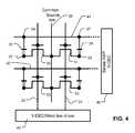
- FIG. 4is a schematic illustration of a memory array, which can be implemented as described herein.
- a common source line 28 , a word line 23 and a word line 24are arranged generally parallel in the Y-direction.
- Bit lines 41 and 42are arranged generally parallel in the X-direction.
- a Y-decoder and a word line driver in block 45are coupled to the word lines 23 , 24 .
- An X-decoder and a set of sense amplifiers in block 46are coupled to the bit lines 41 and 42 .
- the common source line 28is coupled to the source terminals of access transistors 50 , 51 , 52 and 53 .
- the gate of access transistor 50is coupled to the word line 23 .
- the gate of access transistor 51is coupled to the word line 24 .
- the gate of access transistor 52is coupled to the word line 23 .
- the gate of access transistor 53is coupled to the word line 24 .
- the drain of access transistor 50is coupled to the bottom electrode member 32 for pipe-shaped electrode memory cell 35 , which has top electrode member 34 .
- the top electrode member 34is coupled to the bit line 41 .
- the drain of access transistor 51is coupled to the bottom electrode member 33 for pipe-shaped electrode memory cell 36 , which has top electrode member 37 .
- the top electrode member 37is coupled to the bit line 41 .
- Access transistors 52 and 53are coupled to corresponding pipe-shaped electrode memory cells as well on bit line 42 .
- the common source line 28is shared by two rows of memory cells, where a row is arranged in the Y-direction in the illustrated schematic.
- the access transistorscan be replaced by diodes, or other structures for controlling current flow to selected devices in the array for reading and writing data.
- other types of access devices and array structurescan be used.
- FIG. 5is a simplified block diagram of an integrated circuit according to an embodiment of the present invention.
- the integrated circuit 74includes a memory array 60 implemented using pipe-shaped electrode phase change memory cells, on a semiconductor substrate.
- a row decoder 61is coupled to a plurality of word lines 62 , and arranged along rows in the memory array 60 .
- a column decoder 63is coupled to a plurality of bit lines 64 arranged along columns in the memory array 60 for reading and programming data from the memory cells in the array 60 . Addresses are supplied on bus 65 to column decoder 63 and row decoder 61 .
- Sense amplifiers and data-in structures in block 66are coupled to the column decoder 63 via data bus 67 .
- Datais supplied via the data-in line 71 from input/output ports on the integrated circuit 75 or from other data sources internal or external to the integrated circuit 75 , to the data-in structures in block 66 .
- other circuitryis included on the integrated circuit, such as a general purpose processor or special purpose application circuitry, or a combination of modules providing system-on-a-chip functionality supported by the thin film fuse phase change memory cell array.
- Datais supplied via the data-out line 72 from the sense amplifiers in block 66 to input/output ports on the integrated circuit 75 , or to other data destinations internal or external to the integrated circuit 75 .
- a controller implemented in this example using bias arrangement state machine 69controls the application of bias arrangement supply voltages 68 , such as read, program, erase, erase verify and program verify voltages.
- the controllercan be implemented using special-purpose logic circuitry as known in the art.
- the controllercomprises a general-purpose processor, which may be implemented on the same integrated circuit, which executes a computer program to control the operations of the device.
- a combination of special-purpose logic circuitry and a general-purpose processormay be utilized for implementation of the controller.
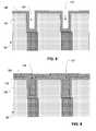
- FIGS. 6-12show stages of a preferred, via-based manufacturing process for pipe-shaped electrode memory cells as shown in FIG. 1 .
- FIG. 6illustrates a top layer of a substrate 99 , including an interlayer dielectric layer 118 having contacts 122 , 123 formed by exposed top surfaces of plugs 120 , 121 that connect underlying access structures (not shown) to the memory cells.
- the substratemay embody a variety of access structures coupled to, or replacing the plugs 120 , 121 , including columnar FET or bipolar transistors or diodes, and planar FETs, diodes, or bipolar junction transistors.
- the interlayer dielectric layer 118comprises a silicon dioxide, silicon nitride or doped silicon oxide material.
- the plug structures 120 , 121comprise tungsten plugs. Other types of conductors can be used as well for the plug structures 120 , 121 as well, including for example aluminum and aluminum alloys, TiN, TaN, TiAlN or TaAlN. Other conductors that might be used comprise one or more elements selected from the group consisting of Ti, W, Mo, Al, Ta, Cu, Pt, Ir, La, Ni, Ru and O.
- a layer 125 of fill material such as silicon dioxideis formed over the surface of the substrate 99 .
- the thickness of the layer 125depends on the ultimate dimensions of the device to be made. For a manufacturing process having a minimum feature size in the range of 50 to 100 nm, the thickness of the layer 125 may be of the same order about 50 to 100 nm, or thicker. Also, other dielectric fill materials may be chosen for compatibility with the subsequent manufacturing processes.
- FIG. 7illustrates a next stage in the process, after patterning and etching vias 126 , 127 over the contacts 122 , 123 .
- a lithographic process, or sub-lithographic process,is used to define the vias 126 , 127 aligned with the underlying contacts 122 , 126 .
- FIG. 8illustrates a next stage in the process after deposition using a conformal process of a layer of electrode material 128 such as titanium nitride as explained above.
- the thickness of the layer of electrode material 128 on the side walls of the vias 126 , 127depends on the ultimate dimensions desired.
- An embodiment in which the diameter of the via is on the order of 5 to 100 nm, the thickness of the electrode layer on the side walls of the via 126 , 127 (corresponding to the thickness T 2 in FIG. 1 )can be on the order of 1 to 20 nm.
- FIG. 9shows a next stage, after deposition of silicon material 129 , such as polysilicon, filling the remaining portions of vias 126 and 127 .
- the silicon material 129can be doped with an n-type material such as phosphorus to enhance its response to thermal oxidation as explained below.
- n-type materialsuch as phosphorus
- other forms of siliconcan be utilized, including amorphous silicon for example.
- FIG. 10illustrates a next stage, after a chemical mechanical polishing process or other planarizing step, which removes the electrode material 128 and the silicon material 129 from the top surface of the structure, leaving the electrode material 128 lining the vias and the silicon material 129 filling the lined vias.
- the structureis exposed to an oxidizing environment which oxidizes the silicon material 129 at a faster rate than the electrode material 128 .
- oxide caps 130 , 131are formed over the layer of silicon material 129 within the vias.
- standard thermal oxidation processescan be utilized.
- Alternative oxidation processesinclude aluminum as the conducting fill material and aluminum oxide as the insulating fill material.
- a nitridation processis used, such as exposing the material to ammonium.
- the resulting structureis subject, if necessary, to chemical mechanical polishing or another planarizing step, to remove any residual oxide or nitride from the top surfaces 132 , 133 of the electrode material 128 .
- the process of manufacturing a memory cell using the electrode with a ring-shaped contact surfaceincludes deposition of a programmable resistance material 135 such as a phase change material, and a top electrode material 136 over the programmable resistance material. Any necessary patterning steps are carried out as required for the particular memory structure be utilized. Finally, back end process steps are executed to complete the integrated circuit, including interlayer dielectric fill processes, metallization processes, capping processes and so on.
- FIGS. 13-18show stages of a pillar-based manufacturing process for pipe-shaped electrode memory cells as shown in FIG. 1 .
- FIG. 13illustrates a structure 99 after front-end-of-line processing. Plugs 120 , 121 are included, formed in corresponding vias that extend through interlayer dielectric layer 118 , to the top surface. At this stage a layer of electrode material 150 has been deposited over the substrate 99 , followed by a layer of silicon, or other oxidizable, conductive material 151 .
- the material 150is planarized by chemical mechanical polishing or otherwise to provide a uniform layer of electrode material over the array region on the integrated circuit.
- the finished layer of material 150has a thickness for example in a range of 20 to 100 nanometers.
- the first electrode material 150may be Ti, Al, W, TiN, Cu, or other metals compatible with the process, selected for good adhesion to the top of the plugs, for adhesion to the second electrode material, and for stability.
- a layer of photoresistis deposited and developed to form photoresist masks have an aerial view shape which is a circular, elliptical or square for example, and are aligned with the plugs 120 and 121 , within the tolerances of the photolithographic process.
- the photoresist masksare trimmed to form smaller masks.
- the photoresist maskscan be etched using an oxygen plasma to form a sub-lithographic, smaller masks which preserve the aerial view shape of the masks, with reduced diameter.
- the smaller masksare used as an etch mask to define pillar structures 152 , 153 , that include respective disc-shaped members comprising material 150 from the electrode layer and respective pillar-shaped silicon members comprising material 151 .
- the pillar-shaped structures 152 , 153have diameters of about 20 to 50 nanometers.
- the disc-shaped members of conductive material 150overlie the tops of the plugs 120 , 121 , and establish good electrical and physical contact with the plugs 120 , 121 .
- FIG. 15illustrates a next stage in the process, after conformal deposition of a layer of a second electrode material 154 over the pillar structures 152 , 153 and over the surface of the substrate.
- the second electrode material 154is the same as the first electrode material 150 .
- the second electrode material 154has higher resistivity than the first electrode material 150 , and good adhesion characteristics to the programmable resistance material.
- the second electrode materialcan be TaN, TiN, AlN, metal oxides such as iridium or lithium oxides, or combinations of materials.
- the second electrode materialcan be deposited using well-known technologies including chemical vapor deposition, sputtering, or other conformal deposition technologies suitable for the selected material.
- a next processing stepincludes anisotropic etching of the layer of material 154 to form sidewall structures on the pillar structures 152 , 153 , while removing the electrode material from the surface of the substrate 99 .
- a fill layer(remaining portions after etchback are labeled 165 ) is deposited followed by an etchback by chemical mechanical polishing, or otherwise, to a level below the tops of the pillar structures 152 , 153 to remove the electrode material from the top of the pillar structures 152 , 153 and establish the height of the pipe-shaped members.
- ring-shaped top surfaces 156 , 157 of the pipe-shaped electrode membersare exposed on a surface of the resulting structure.
- the height of the pipe-shaped electrode members in a representative embodimentis about 80 to 150 nanometers, such as about 100 nanometers.
- the thickness of the sidewalls of the pipe-shaped electrode members of electrode material 154is between about 10 and 30 nanometers, such as about 20 nanometers.
- the thickness of the disc-shaped members of electrode material 150 from layercan be therefore at least twice the thickness of the sidewalls on the pipe-shaped electrode members for example.
- FIG. 18illustrates a structure after depositing, by sputtering for example, a conformal layer 158 of GST, or other programmable resistance material, over the surface of the fill layer 165 .
- GSTcan be deposited using sputtering with collimation at about 250 degrees C.
- the GSTcan be deposited using a metal organic chemical vapor deposition (MO-CVD) process.
- MO-CVDmetal organic chemical vapor deposition
- the conformal layer 158comprises a thin film having a thickness of about 30 to 100 nanometers.
- a layer 159 of electrode materialwhich can be the same as the electrode material 150 , is deposited over the layer 158 , having a thickness in the range of 30 to 100 nanometers.
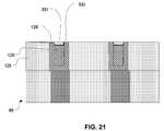
- FIGS. 19-21illustrate stages in a process involving a recess etched/fill technique for making the insulating cap member 13 .
- the stagesstart after the stage shown in FIG. 10 or in FIG. 17 .
- a chemical mechanical polishing process or other planarizing stepleaves the electrode material 128 lining the vias through layer 125 , and the conducting fill material 129 filling the lined vias.
- FIG. 19illustrates a structure resulting after a recess etch which selectively removes the conducting fill material, and leaves a recess 229 .
- an insulating fill material 230is deposited over the structure, filling the recess to 229 .
- a chemical mechanical polishing process or other similar planarizing processis executed, so that a top surface 331 of the insulating fill material is flush with a top surface 332 of the pipe-shaped or trench-shaped member formed by electrode material 128 .
- the structure of the memory devicecan be completed as described above.
- the insulating fill materialis chosen for process compatibility factors and is not necessarily an oxide or nitride of the conducting fill material.
- the pipe-shaped memberhas sides that are continuous around the perimeter of the cell.
- a rectangular pipe-shaped memberis formed, so that it can be characterized as a trench-shaped member.
- deposition techniquescould be used to make the pipe-shaped or trench-shaped member discontinuous around the sides, further reducing the volume the active regions.
Landscapes
- Engineering & Computer Science (AREA)
- Manufacturing & Machinery (AREA)
- Chemical & Material Sciences (AREA)
- Crystallography & Structural Chemistry (AREA)
- Semiconductor Memories (AREA)
Abstract
Description
Claims (13)
Priority Applications (3)
| Application Number | Priority Date | Filing Date | Title |
|---|---|---|---|
| US12/426,809US8084760B2 (en) | 2009-04-20 | 2009-04-20 | Ring-shaped electrode and manufacturing method for same |
| TW098144272ATWI415299B (en) | 2009-04-20 | 2009-12-22 | Ring-shaped electrode and munufacturing method for same |
| CN2010101654103ACN101866942B (en) | 2009-04-20 | 2010-04-20 | Ring electrode and method for manufacturing the same |
Applications Claiming Priority (1)
| Application Number | Priority Date | Filing Date | Title |
|---|---|---|---|
| US12/426,809US8084760B2 (en) | 2009-04-20 | 2009-04-20 | Ring-shaped electrode and manufacturing method for same |
Publications (2)
| Publication Number | Publication Date |
|---|---|
| US20100264396A1 US20100264396A1 (en) | 2010-10-21 |
| US8084760B2true US8084760B2 (en) | 2011-12-27 |
Family
ID=42958579
Family Applications (1)
| Application Number | Title | Priority Date | Filing Date |
|---|---|---|---|
| US12/426,809Active2029-07-02US8084760B2 (en) | 2009-04-20 | 2009-04-20 | Ring-shaped electrode and manufacturing method for same |
Country Status (3)
| Country | Link |
|---|---|
| US (1) | US8084760B2 (en) |
| CN (1) | CN101866942B (en) |
| TW (1) | TWI415299B (en) |
Cited By (9)
| Publication number | Priority date | Publication date | Assignee | Title |
|---|---|---|---|---|
| US8816314B2 (en) | 2011-05-13 | 2014-08-26 | Adesto Technologies Corporation | Contact structure and method for variable impedance memory element |
| US8829482B1 (en) | 2010-09-23 | 2014-09-09 | Adesto Technologies Corporation | Variable impedance memory device structure and method of manufacture including programmable impedance memory cells and methods of forming the same |
| US8847191B1 (en) | 2012-03-27 | 2014-09-30 | Adesto Technologies Corporation | Programmable impedance memory elements, methods of manufacture, and memory devices containing the same |
| US20140291597A1 (en)* | 2012-09-11 | 2014-10-02 | Shanghai Institute Of Microsystem And Information Technology, Chinese Academy | High-speed, High-density, and Low-power consumption Phase-change Memory Unit, and Preparation Method Thereof |
| US20160064656A1 (en)* | 2014-08-28 | 2016-03-03 | Taiwan Semiconductor Manufacturing Co., Ltd. | Phase Change Memory Structure to Reduce Leakage from the Heating Element to the Surrounding Material |
| US9515251B2 (en) | 2014-04-09 | 2016-12-06 | International Business Machines Corporation | Structure for thermally assisted MRAM |
| US9691816B2 (en) | 2015-01-22 | 2017-06-27 | Samsung Electronics Co., Ltd. | Magnetic memory devices |
| US10490744B2 (en) | 2017-11-07 | 2019-11-26 | Macronix International Co., Ltd. | Contact hole structure method for fabricating the same and applications thereof |
| US10644232B2 (en) | 2017-12-28 | 2020-05-05 | International Business Machines Corporation | Self-aligned and misalignment-tolerant landing pad for magnetoresistive random access memory |
Families Citing this family (27)
| Publication number | Priority date | Publication date | Assignee | Title |
|---|---|---|---|---|
| KR101602007B1 (en)* | 2009-07-02 | 2016-03-09 | 인티그리스, 인코포레이티드 | Hollow gst structure with dielectric fill |
| US8183126B2 (en)* | 2009-07-13 | 2012-05-22 | Seagate Technology Llc | Patterning embedded control lines for vertically stacked semiconductor elements |
| US9171613B2 (en)* | 2009-07-28 | 2015-10-27 | Hewlett-Packard Development Company, L.P. | Memristors with asymmetric electrodes |
| CN102664236B (en)* | 2012-05-16 | 2014-09-10 | 中国科学院上海微系统与信息技术研究所 | Ring electrode structure for low-power-consumption phase change memory and preparation method |
| US9640757B2 (en) | 2012-10-30 | 2017-05-02 | Entegris, Inc. | Double self-aligned phase change memory device structure |
| US9444040B2 (en) | 2013-03-13 | 2016-09-13 | Microchip Technology Incorporated | Sidewall type memory cell |
| US9362496B2 (en)* | 2013-03-13 | 2016-06-07 | Microchip Technology Incorporated | Resistive memory cell with trench-shaped bottom electrode |
| US20140264247A1 (en)* | 2013-03-13 | 2014-09-18 | Microchip Technology Incorporated | Resistive Memory Cell with Reduced Bottom Electrode |
| CN103500795B (en)* | 2013-09-30 | 2015-07-22 | 上海新安纳电子科技有限公司 | Preparation method of phase change memory electrode structure |
| US10003021B2 (en) | 2014-02-19 | 2018-06-19 | Microchip Technology Incorporated | Resistive memory cell with sloped bottom electrode |
| US9269606B2 (en) | 2014-02-19 | 2016-02-23 | Microchip Technology Incorporated | Spacer enabled active isolation for an integrated circuit device |
| US9385313B2 (en) | 2014-02-19 | 2016-07-05 | Microchip Technology Incorporated | Resistive memory cell having a reduced conductive path area |
| US9318702B2 (en) | 2014-02-19 | 2016-04-19 | Microchip Technology Incorporated | Resistive memory cell having a reduced conductive path area |
| US9412942B2 (en) | 2014-02-19 | 2016-08-09 | Microchip Technology Incorporated | Resistive memory cell with bottom electrode having a sloped side wall |
| CN105098068A (en)* | 2014-05-22 | 2015-11-25 | 中芯国际集成电路制造(上海)有限公司 | Semiconductor device, manufacturing method thereof and electronic device |
| JP2018500754A (en) | 2014-11-26 | 2018-01-11 | マイクロチップ テクノロジー インコーポレイテッドMicrochip Technology Incorporated | Resistive memory cell with spacer region for reduced conductive path area / increased electric field |
| US10134984B1 (en)* | 2014-12-31 | 2018-11-20 | Crossbar, Inc. | Two-terminal memory electrode comprising a non-continuous contact surface |
| US9406883B1 (en)* | 2015-01-08 | 2016-08-02 | Taiwan Semiconductor Manufacturing Co., Ltd | Structure and formation method of memory device |
| JP6563689B2 (en)* | 2015-05-27 | 2019-08-21 | トヨタ自動車株式会社 | Insulated gate type switching device manufacturing method |
| CN106192982B (en)* | 2016-07-11 | 2019-05-31 | 河海大学 | A method of the electric osmose soil stake based on tubulose ekg electrode handles soft base |
| US10510954B2 (en)* | 2017-11-28 | 2019-12-17 | Taiwan Semiconductor Manufacturing Co., Ltd. | Phase change random access memory device |
| CN108447987B (en)* | 2018-04-27 | 2020-02-14 | 中山大学 | Preparation method of low-activation-voltage resistance change device |
| CN109411601B (en)* | 2018-11-06 | 2023-04-07 | 珠海创飞芯科技有限公司 | Resistive random access memory and manufacturing method thereof |
| CN109786550B (en)* | 2019-03-18 | 2024-04-05 | 北京时代全芯存储技术股份有限公司 | Phase change memory and method for manufacturing the same |
| CN112736198B (en)* | 2020-12-31 | 2023-06-02 | 上海集成电路装备材料产业创新中心有限公司 | Resistive random access memory and preparation method thereof |
| US12075627B2 (en) | 2021-08-26 | 2024-08-27 | International Business Machines Corporation | AI accelerator with MRAM, PCM, and recessed PCM bottom electrode |
| CN115747931A (en)* | 2022-11-30 | 2023-03-07 | 诸暨市中俄联合材料实验室 | Tubular electrode for oxidation treatment of blind hole structure |
Citations (305)
| Publication number | Priority date | Publication date | Assignee | Title |
|---|---|---|---|---|
| US3271591A (en) | 1963-09-20 | 1966-09-06 | Energy Conversion Devices Inc | Symmetrical current controlling device |
| US3530441A (en) | 1969-01-15 | 1970-09-22 | Energy Conversion Devices Inc | Method and apparatus for storing and retrieving information |
| US4452592A (en) | 1982-06-01 | 1984-06-05 | General Motors Corporation | Cyclic phase change coupling |
| US4599705A (en) | 1979-12-13 | 1986-07-08 | Energy Conversion Devices, Inc. | Programmable cell for use in programmable electronic arrays |
| US4719594A (en) | 1984-11-01 | 1988-01-12 | Energy Conversion Devices, Inc. | Grooved optical data storage device including a chalcogenide memory layer |
| US4769339A (en) | 1983-12-26 | 1988-09-06 | Kabushiki Kaisha Toshiba | Method of manufacturing a field effect transistor device having a multilayer gate electrode |
| US4876220A (en) | 1986-05-16 | 1989-10-24 | Actel Corporation | Method of making programmable low impedance interconnect diode element |
| US4959812A (en) | 1987-12-28 | 1990-09-25 | Kabushiki Kaisha Toshiba | Electrically erasable programmable read-only memory with NAND cell structure |
| US5106775A (en) | 1987-12-10 | 1992-04-21 | Hitachi, Ltd. | Process for manufacturing vertical dynamic random access memories |
| US5166758A (en) | 1991-01-18 | 1992-11-24 | Energy Conversion Devices, Inc. | Electrically erasable phase change memory |
| US5166096A (en) | 1991-10-29 | 1992-11-24 | International Business Machines Corporation | Process for fabricating self-aligned contact studs for semiconductor structures |
| US5177567A (en) | 1991-07-19 | 1993-01-05 | Energy Conversion Devices, Inc. | Thin-film structure for chalcogenide electrical switching devices and process therefor |
| US5332923A (en) | 1991-08-06 | 1994-07-26 | Nec Corporation | Semiconductor memory |
| US5391901A (en) | 1992-10-30 | 1995-02-21 | Nec Corporation | Semiconductor memory with oblique folded bit-line arrangement |
| US5515488A (en) | 1994-08-30 | 1996-05-07 | Xerox Corporation | Method and apparatus for concurrent graphical visualization of a database search and its search history |
| US5534712A (en) | 1991-01-18 | 1996-07-09 | Energy Conversion Devices, Inc. | Electrically erasable memory elements characterized by reduced current and improved thermal stability |
| US5550396A (en) | 1992-01-24 | 1996-08-27 | Mitsubishi Denki Kabushiki Kaisha | Vertical field effect transistor with a trench structure |
| US5687112A (en) | 1996-04-19 | 1997-11-11 | Energy Conversion Devices, Inc. | Multibit single cell memory element having tapered contact |
| US5688713A (en) | 1996-08-26 | 1997-11-18 | Vanguard International Semiconductor Corporation | Method of manufacturing a DRAM cell having a double-crown capacitor using polysilicon and nitride spacers |
| US5716883A (en) | 1996-11-06 | 1998-02-10 | Vanguard International Semiconductor Corporation | Method of making increased surface area, storage node electrode, with narrow spaces between polysilicon columns |
| US5754472A (en) | 1995-12-27 | 1998-05-19 | Hyundai Electronics Industries Co., Ltd. | Flash memory device having a program path the same as a read pre-condition path |
| US5789758A (en) | 1995-06-07 | 1998-08-04 | Micron Technology, Inc. | Chalcogenide memory cell with a plurality of chalcogenide electrodes |
| US5789277A (en) | 1996-07-22 | 1998-08-04 | Micron Technology, Inc. | Method of making chalogenide memory device |
| US5814527A (en) | 1996-07-22 | 1998-09-29 | Micron Technology, Inc. | Method of making small pores defined by a disposable internal spacer for use in chalcogenide memories |
| US5831276A (en) | 1995-06-07 | 1998-11-03 | Micron Technology, Inc. | Three-dimensional container diode for use with multi-state material in a non-volatile memory cell |
| US5837564A (en) | 1995-11-01 | 1998-11-17 | Micron Technology, Inc. | Method for optimal crystallization to obtain high electrical performance from chalcogenides |
| US5869843A (en) | 1995-06-07 | 1999-02-09 | Micron Technology, Inc. | Memory array having a multi-state element and method for forming such array or cells thereof |
| US5879955A (en) | 1995-06-07 | 1999-03-09 | Micron Technology, Inc. | Method for fabricating an array of ultra-small pores for chalcogenide memory cells |
| US5902704A (en) | 1997-07-02 | 1999-05-11 | Lsi Logic Corporation | Process for forming photoresist mask over integrated circuit structures with critical dimension control |
| US5933365A (en) | 1997-06-19 | 1999-08-03 | Energy Conversion Devices, Inc. | Memory element with energy control mechanism |
| US5952671A (en) | 1997-05-09 | 1999-09-14 | Micron Technology, Inc. | Small electrode for a chalcogenide switching device and method for fabricating same |
| US5958358A (en) | 1992-07-08 | 1999-09-28 | Yeda Research And Development Co., Ltd. | Oriented polycrystalline thin films of transition metal chalcogenides |
| US5970336A (en) | 1996-08-22 | 1999-10-19 | Micron Technology, Inc. | Method of making memory cell incorporating a chalcogenide element |
| US5985698A (en) | 1996-07-22 | 1999-11-16 | Micron Technology, Inc. | Fabrication of three dimensional container diode for use with multi-state material in a non-volatile memory cell |
| US6011725A (en) | 1997-08-01 | 2000-01-04 | Saifun Semiconductors, Ltd. | Two bit non-volatile electrically erasable and programmable semiconductor memory cell utilizing asymmetrical charge trapping |
| US6025220A (en) | 1996-06-18 | 2000-02-15 | Micron Technology, Inc. | Method of forming a polysilicon diode and devices incorporating such diode |
| US6031287A (en) | 1997-06-18 | 2000-02-29 | Micron Technology, Inc. | Contact structure and memory element incorporating the same |
| US6034882A (en) | 1998-11-16 | 2000-03-07 | Matrix Semiconductor, Inc. | Vertically stacked field programmable nonvolatile memory and method of fabrication |
| US6046951A (en) | 1998-01-23 | 2000-04-04 | Stmicroelectronics S.A. | Process for controlling the read circuit of a memory plane and corresponding memory device |
| US6066870A (en) | 1996-07-16 | 2000-05-23 | Micron Technology, Inc. | Single digit line with cell contact interconnect |
| US6075719A (en) | 1999-06-22 | 2000-06-13 | Energy Conversion Devices, Inc. | Method of programming phase-change memory element |
| US6077674A (en) | 1999-10-27 | 2000-06-20 | Agilent Technologies Inc. | Method of producing oligonucleotide arrays with features of high purity |
| US6087269A (en) | 1998-04-20 | 2000-07-11 | Advanced Micro Devices, Inc. | Method of making an interconnect using a tungsten hard mask |
| US6087674A (en) | 1996-10-28 | 2000-07-11 | Energy Conversion Devices, Inc. | Memory element with memory material comprising phase-change material and dielectric material |
| US6114713A (en) | 1997-01-28 | 2000-09-05 | Zahorik; Russell C. | Integrated circuit memory cell having a small active area and method of forming same |
| US6117720A (en) | 1995-06-07 | 2000-09-12 | Micron Technology, Inc. | Method of making an integrated circuit electrode having a reduced contact area |
| US6147395A (en) | 1996-10-02 | 2000-11-14 | Micron Technology, Inc. | Method for fabricating a small area of contact between electrodes |
| US6177317B1 (en) | 1999-04-14 | 2001-01-23 | Macronix International Co., Ltd. | Method of making nonvolatile memory devices having reduced resistance diffusion regions |
| US6271090B1 (en) | 2000-12-22 | 2001-08-07 | Macronix International Co., Ltd. | Method for manufacturing flash memory device with dual floating gates and two bits per cell |
| US6280684B1 (en) | 1994-12-13 | 2001-08-28 | Ricoh Company, Ltd. | Sputtering target, method of producing the target, optical recording medium fabricated by using the sputtering target, and method of fabricating the optical recording medium |
| US6291137B1 (en) | 1999-01-20 | 2001-09-18 | Advanced Micro Devices, Inc. | Sidewall formation for sidewall patterning of sub 100 nm structures |
| US6314014B1 (en) | 1999-12-16 | 2001-11-06 | Ovonyx, Inc. | Programmable resistance memory arrays with reference cells |
| US6316348B1 (en) | 1999-02-05 | 2001-11-13 | Taiwan Semiconductor Manufacturing Company | High selectivity Si-rich SiON etch-stop layer |
| US6320786B1 (en) | 2000-12-22 | 2001-11-20 | Macronix International Co., Ltd. | Method of controlling multi-state NROM |
| US6326307B1 (en) | 1999-11-15 | 2001-12-04 | Appllied Materials, Inc. | Plasma pretreatment of photoresist in an oxide etch process |
| US6337266B1 (en) | 1996-07-22 | 2002-01-08 | Micron Technology, Inc. | Small electrode for chalcogenide memories |
| US6339544B1 (en) | 2000-09-29 | 2002-01-15 | Intel Corporation | Method to enhance performance of thermal resistor device |
| US6351406B1 (en) | 1998-11-16 | 2002-02-26 | Matrix Semiconductor, Inc. | Vertically stacked field programmable nonvolatile memory and method of fabrication |
| US6372651B1 (en) | 1998-07-17 | 2002-04-16 | Advanced Micro Devices, Inc. | Method for trimming a photoresist pattern line for memory gate etching |
| US6380068B2 (en) | 2000-01-05 | 2002-04-30 | Macronix International Co., Ltd. | Method for planarizing a flash memory device |
| US20020070457A1 (en) | 2000-12-09 | 2002-06-13 | Samsung Electronics Co., Ltd. | Metal contact structure in semiconductor device and method for forming the same |
| US20020079483A1 (en) | 2000-12-26 | 2002-06-27 | Charles Dennison | Phase-change memory bipolar array utilizing a single shallow trench isolation for creating an individual active area region for two memory array elements and one bipolar base contact |
| US6420215B1 (en) | 2000-04-28 | 2002-07-16 | Matrix Semiconductor, Inc. | Three-dimensional memory array and method of fabrication |
| US6420216B1 (en) | 2000-03-14 | 2002-07-16 | International Business Machines Corporation | Fuse processing using dielectric planarization pillars |
| US6429064B1 (en) | 2000-09-29 | 2002-08-06 | Intel Corporation | Reduced contact area of sidewall conductor |
| US20020113273A1 (en) | 2001-02-22 | 2002-08-22 | Samsung Electronics Co., Ltd. | Semiconductor device having contact plug and method for manufacturing the same |
| US6440837B1 (en) | 2000-07-14 | 2002-08-27 | Micron Technology, Inc. | Method of forming a contact structure in a semiconductor device |
| US6483736B2 (en) | 1998-11-16 | 2002-11-19 | Matrix Semiconductor, Inc. | Vertically stacked field programmable nonvolatile memory and method of fabrication |
| US6487106B1 (en) | 1999-01-12 | 2002-11-26 | Arizona Board Of Regents | Programmable microelectronic devices and method of forming and programming same |
| US6487114B2 (en) | 2001-02-28 | 2002-11-26 | Macronix International Co., Ltd. | Method of reading two-bit memories of NROM cell |
| US6501111B1 (en) | 2000-06-30 | 2002-12-31 | Intel Corporation | Three-dimensional (3D) programmable device |
| US6512241B1 (en) | 2001-12-31 | 2003-01-28 | Intel Corporation | Phase change material memory device |
| US6512263B1 (en) | 2000-09-22 | 2003-01-28 | Sandisk Corporation | Non-volatile memory cell array having discontinuous source and drain diffusions contacted by continuous bit line conductors and methods of forming |
| US6511867B2 (en) | 2001-06-30 | 2003-01-28 | Ovonyx, Inc. | Utilizing atomic layer deposition for programmable device |
| US6514820B2 (en) | 1998-08-27 | 2003-02-04 | Micron Technology, Inc. | Method for forming single electron resistor memory |
| US6514788B2 (en) | 2001-05-29 | 2003-02-04 | Bae Systems Information And Electronic Systems Integration Inc. | Method for manufacturing contacts for a Chalcogenide memory device |
| US6545903B1 (en) | 2001-12-17 | 2003-04-08 | Texas Instruments Incorporated | Self-aligned resistive plugs for forming memory cell with phase change material |
| US20030072195A1 (en) | 2001-06-12 | 2003-04-17 | Thomas Mikolajick | Semiconductor memory device and fabrication method |
| US6551866B1 (en) | 1998-11-27 | 2003-04-22 | Mitsubishi Denki Kabushiki Kaisha | Method of manufacturing a semiconductor memory device |
| US6555860B2 (en) | 2000-09-29 | 2003-04-29 | Intel Corporation | Compositionally modified resistive electrode |
| US6563156B2 (en) | 2001-03-15 | 2003-05-13 | Micron Technology, Inc. | Memory elements and methods for making same |
| US6566700B2 (en) | 2001-10-11 | 2003-05-20 | Ovonyx, Inc. | Carbon-containing interfacial layer for phase-change memory |
| US6567293B1 (en) | 2000-09-29 | 2003-05-20 | Ovonyx, Inc. | Single level metal memory cell using chalcogenide cladding |
| US20030095426A1 (en) | 2001-11-20 | 2003-05-22 | Glen Hush | Complementary bit PCRAM sense amplifier and method of operation |
| US6576546B2 (en) | 1999-12-22 | 2003-06-10 | Texas Instruments Incorporated | Method of enhancing adhesion of a conductive barrier layer to an underlying conductive plug and contact for ferroelectric applications |
| US6579760B1 (en) | 2002-03-28 | 2003-06-17 | Macronix International Co., Ltd. | Self-aligned, programmable phase change memory |
| US6586761B2 (en) | 2001-09-07 | 2003-07-01 | Intel Corporation | Phase change material memory device |
| US6589714B2 (en) | 2001-06-26 | 2003-07-08 | Ovonyx, Inc. | Method for making programmable resistance memory element using silylated photoresist |
| US6596589B2 (en) | 2001-04-30 | 2003-07-22 | Vanguard International Semiconductor Corporation | Method of manufacturing a high coupling ratio stacked gate flash memory with an HSG-SI layer |
| US6605527B2 (en) | 2001-06-30 | 2003-08-12 | Intel Corporation | Reduced area intersection between electrode and programming element |
| US6605821B1 (en) | 2002-05-10 | 2003-08-12 | Hewlett-Packard Development Company, L.P. | Phase change material electronic memory structure and method for forming |
| US6613604B2 (en) | 2001-08-02 | 2003-09-02 | Ovonyx, Inc. | Method for making small pore for use in programmable resistance memory element |
| US6617192B1 (en) | 1997-10-01 | 2003-09-09 | Ovonyx, Inc. | Electrically programmable memory element with multi-regioned contact |
| US6627530B2 (en) | 2000-12-22 | 2003-09-30 | Matrix Semiconductor, Inc. | Patterning three dimensional structures |
| US6639849B2 (en) | 2002-02-28 | 2003-10-28 | Fujitsu Limited | Nonvolatile semiconductor memory device programming second dynamic reference cell according to threshold value of first dynamic reference cell |
| US6674115B2 (en) | 2001-08-31 | 2004-01-06 | Intel Corporation | Multiple layer phrase-change memory |
| US6673700B2 (en) | 2001-06-30 | 2004-01-06 | Ovonyx, Inc. | Reduced area intersection between electrode and programming element |
| US6677678B2 (en) | 2000-03-14 | 2004-01-13 | International Business Machines Corporation | Damascene structure using a sacrificial conductive layer |
| US20040026686A1 (en) | 2002-08-09 | 2004-02-12 | Macronix International Co., Ltd. | Spacer chalcogenide memory method and device |
| US20040051094A1 (en) | 2002-09-13 | 2004-03-18 | Mitsubishi Denki Kabushiki Kaisha | Non-volatile semiconductor memory device allowing shrinking of memory cell |
| US6744088B1 (en) | 2002-12-13 | 2004-06-01 | Intel Corporation | Phase change memory device on a planar composite layer |
| US6750079B2 (en) | 1999-03-25 | 2004-06-15 | Ovonyx, Inc. | Method for making programmable resistance memory element |
| US20040113137A1 (en) | 2002-12-13 | 2004-06-17 | Lowrey Tyler A. | Memory and access device and method therefor |
| US20040165422A1 (en) | 2003-02-24 | 2004-08-26 | Horii Hideki | Phase changeable memory devices and methods for fabricating the same |
| US6791102B2 (en) | 2002-12-13 | 2004-09-14 | Intel Corporation | Phase change memory |
| US6797979B2 (en) | 2000-12-21 | 2004-09-28 | Intel Corporation | Metal structure for a phase-change memory device |
| US6800504B2 (en) | 2001-08-30 | 2004-10-05 | Micron Technology, Inc. | Integrated circuit device and fabrication using metal-doped chalcogenide materials |
| US6800563B2 (en) | 2001-10-11 | 2004-10-05 | Ovonyx, Inc. | Forming tapered lower electrode phase-change memories |
| US6815704B1 (en) | 2003-09-04 | 2004-11-09 | Silicon Storage Technology, Inc. | Phase change memory device employing thermally insulating voids |
| US20040248339A1 (en) | 2003-06-06 | 2004-12-09 | Lung Hsiang Lan | High density chalcogenide memory cells |
| US20040256610A1 (en) | 2003-06-23 | 2004-12-23 | Hsiang-Lan Lung | Chalcogenide memory device with multiple bits per cell |
| US20050018526A1 (en) | 2003-07-21 | 2005-01-27 | Heon Lee | Phase-change memory device and manufacturing method thereof |
| US6850432B2 (en) | 2002-08-20 | 2005-02-01 | Macronix International Co., Ltd. | Laser programmable electrically readable phase-change memory method and device |
| US20050029502A1 (en) | 2003-08-04 | 2005-02-10 | Hudgens Stephen J. | Processing phase change material to improve programming speed |
| US6859389B2 (en) | 2002-10-31 | 2005-02-22 | Dai Nippon Printing Co., Ltd. | Phase change-type memory element and process for producing the same |
| US6861267B2 (en) | 2001-09-17 | 2005-03-01 | Intel Corporation | Reducing shunts in memories with phase-change material |
| US6864500B2 (en) | 2002-04-10 | 2005-03-08 | Micron Technology, Inc. | Programmable conductor memory cell structure |
| US20050052904A1 (en) | 2003-09-08 | 2005-03-10 | Samsung Electronics Co., Ltd. | Initial firing method and phase change memory device for performing firing effectively |
| US6867638B2 (en) | 2002-01-10 | 2005-03-15 | Silicon Storage Technology, Inc. | High voltage generation and regulation system for digital multilevel nonvolatile memory |
| US20050062087A1 (en) | 2003-09-19 | 2005-03-24 | Yi-Chou Chen | Chalcogenide phase-change non-volatile memory, memory device and method for fabricating the same |
| US6888750B2 (en) | 2000-04-28 | 2005-05-03 | Matrix Semiconductor, Inc. | Nonvolatile memory on SOI and compound semiconductor substrates and method of fabrication |
| US6894305B2 (en) | 2003-02-24 | 2005-05-17 | Samsung Electronics Co., Ltd. | Phase-change memory devices with a self-heater structure |
| US6894304B2 (en) | 2001-08-27 | 2005-05-17 | Micron Technology, Inc. | Apparatus and method for dual cell common electrode PCRAM memory device |
| US6900517B2 (en) | 2002-04-09 | 2005-05-31 | Matsushita Electric Industrial Co., Ltd. | Non-volatile memory with phase-change recording layer |
| US6903362B2 (en) | 2001-05-09 | 2005-06-07 | Science Applications International Corporation | Phase change switches and circuits coupling to electromagnetic waves containing phase change switches |
| US20050127349A1 (en) | 2003-12-10 | 2005-06-16 | Horak David V. | Phase change tip storage cell |
| US20050127347A1 (en) | 2003-12-12 | 2005-06-16 | Suk-Hun Choi | Methods for fabricating memory devices using sacrificial layers and memory devices fabricated by same |
| US6909107B2 (en) | 2002-12-30 | 2005-06-21 | Bae Systems, Information And Electronic Systems Integration, Inc. | Method for manufacturing sidewall contacts for a chalcogenide memory device |
| US6910907B2 (en) | 2003-11-18 | 2005-06-28 | Agere Systems Inc. | Contact for use in an integrated circuit and a method of manufacture therefor |
| US20050141261A1 (en) | 2003-12-30 | 2005-06-30 | Su-Jin Ahn | Set programming methods and write driver circuits for a phase-change memory array |
| US20050145984A1 (en) | 2004-01-06 | 2005-07-07 | Yi-Chou Chen | Horizontal chalcogenide element defined by a pad for use in solid-state memories |
| US20050167656A1 (en) | 2004-01-30 | 2005-08-04 | International Business Machines Corporation | Phase-change memory cell and method of fabricating the phase-change memory cell |
| US6928022B2 (en) | 2003-11-27 | 2005-08-09 | Samsung Electronics Co., Ltd. | Write driver circuit in phase change memory device and method for applying write current |
| US6927410B2 (en) | 2003-09-04 | 2005-08-09 | Silicon Storage Technology, Inc. | Memory device with discrete layers of phase change memory material |
| US6937507B2 (en) | 2003-12-05 | 2005-08-30 | Silicon Storage Technology, Inc. | Memory device and method of operating same |
| US6936544B2 (en) | 2003-03-11 | 2005-08-30 | Taiwan Semiconductor Manufacturing Co., Ltd. | Method of removing metal etching residues following a metal etchback process to improve a CMP process |
| US20050191804A1 (en) | 2004-03-01 | 2005-09-01 | Taiwan Semiconductor Manufacturing Co., Ltd. | Method for forming a reduced active area in a phase change memory structure |
| US20050195633A1 (en) | 2004-03-05 | 2005-09-08 | Byung-Gil Choi | Method for programming phase-change memory array to set state and circuit of a phase-change memory device |
| US6943365B2 (en) | 1999-03-25 | 2005-09-13 | Ovonyx, Inc. | Electrically programmable memory element with reduced area of contact and method for making same |
| US20050201182A1 (en) | 2004-03-12 | 2005-09-15 | Kenichi Osada | Semiconductor device |
| US20050212026A1 (en) | 2004-03-26 | 2005-09-29 | Suk-Jin Chung | Trench capacitors with insulating layer collars in undercut regions and method of fabricating the same |
| US20050215009A1 (en) | 2004-03-19 | 2005-09-29 | Sung-Lae Cho | Methods of forming phase-change memory devices |
| US20050212024A1 (en) | 2004-03-24 | 2005-09-29 | Infineon Technologies Ag | Memory device with an active material embedded in an insulating material |
| US6969866B1 (en) | 1997-10-01 | 2005-11-29 | Ovonyx, Inc. | Electrically programmable memory element with improved contacts |
| US20050263829A1 (en) | 2004-05-27 | 2005-12-01 | Yoon-Jong Song | Semiconductor devices having phase change memory cells, electronic systems employing the same and methods of fabricating the same |
| US6972430B2 (en) | 2002-02-20 | 2005-12-06 | Stmicroelectronics S.R.L. | Sublithographic contact structure, phase change memory cell with optimized heater shape, and manufacturing method thereof |
| US6972428B2 (en) | 2001-06-26 | 2005-12-06 | Ovonyx, Inc. | Programmable resistance memory element |
| US6977181B1 (en) | 2004-06-17 | 2005-12-20 | Infincon Technologies Ag | MTJ stack with crystallization inhibiting layer |
| US20060006472A1 (en) | 2003-06-03 | 2006-01-12 | Hai Jiang | Phase change memory with extra-small resistors |
| US6992932B2 (en) | 2002-10-29 | 2006-01-31 | Saifun Semiconductors Ltd | Method circuit and system for read error detection in a non-volatile memory array |
| US20060038221A1 (en) | 2004-08-21 | 2006-02-23 | Samsung Electronics Co., Ltd. | Antiferromagnetic/paramagnetic resistive device, non-volatile memory and method for fabricating the same |
| US20060066156A1 (en) | 2004-09-30 | 2006-03-30 | Dong Qimin J | Motor rotor cooling with rotation heat pipes |
| US7023009B2 (en) | 1997-10-01 | 2006-04-04 | Ovonyx, Inc. | Electrically programmable memory element with improved contacts |
| US20060073642A1 (en) | 2003-07-21 | 2006-04-06 | Macronix International Co., Ltd. | Method for manufacturing a multiple-bit-per-cell memory |
| US7038938B2 (en) | 2003-12-13 | 2006-05-02 | Hynix Semiconductor Inc. | Phase change resistor cell and nonvolatile memory device using the same |
| US20060094154A1 (en) | 2004-10-29 | 2006-05-04 | Hsiang-Lan Lung | Common word line edge contact phase-change memory |
| US20060091476A1 (en) | 2004-10-29 | 2006-05-04 | Cay-Uwe Pinnow | Sub-lithographic structures, devices including such structures, and methods for producing the same |
| US7042001B2 (en) | 2004-01-29 | 2006-05-09 | Samsung Electronics Co., Ltd. | Phase change memory devices including memory elements having variable cross-sectional areas |
| US20060110878A1 (en) | 2004-11-22 | 2006-05-25 | Macronix International Co., Ltd. | Side wall active pin memory and manufacturing method |
| US20060110888A1 (en) | 2004-10-19 | 2006-05-25 | Byeong-Ok Cho | Phase changeable memory device and method of formation thereof |
| US7054183B2 (en) | 2002-10-31 | 2006-05-30 | Unity Semiconductor Corporation | Adaptive programming technique for a re-writable conductive memory device |
| US20060113521A1 (en) | 2004-11-30 | 2006-06-01 | Hsiang-Lan Lung | Chalcogenide memory having a small active region |
| US20060113520A1 (en) | 2004-12-01 | 2006-06-01 | Renesas Technology Corp. | Semiconductor integrated circuit device and method of manufacturing the same |
| US20060118913A1 (en) | 2004-12-06 | 2006-06-08 | Samsung Electronics Co., Ltd. | Phase changeable memory cells and methods of forming the same |
| US20060124916A1 (en) | 2004-12-09 | 2006-06-15 | Macronix International Co., Ltd. | Self-aligned small contact phase-change memory method and device |
| US20060126395A1 (en) | 2004-12-10 | 2006-06-15 | Shih-Hung Chen | Non-volatile memory cell and operating method thereof |
| US20060131555A1 (en) | 2004-12-22 | 2006-06-22 | Micron Technology, Inc. | Resistance variable devices with controllable channels |
| US7067864B2 (en) | 2001-01-30 | 2006-06-27 | Renesas Technology Corp. | SRAM having an improved capacitor |
| US7067837B2 (en) | 2003-04-02 | 2006-06-27 | Samsung Electronics Co., Ltd. | Phase-change memory devices |
| US20060138467A1 (en) | 2004-12-29 | 2006-06-29 | Hsiang-Lan Lung | Method of forming a small contact in phase-change memory and a memory cell produced by the method |
| US20060154185A1 (en) | 2005-01-11 | 2006-07-13 | Taiwan Semiconductor Manufacturing Co., Ltd. | Method for forming a finely patterned resist |
| US7078273B2 (en) | 2002-02-01 | 2006-07-18 | Hitachi, Ltd. | Semiconductor memory cell and method of forming same |
| US20060157680A1 (en) | 2003-05-22 | 2006-07-20 | Norikatsu Takaura | Semiconductor integrated circuit device |
| US20060163554A1 (en) | 2002-10-11 | 2006-07-27 | Koninklijke Philips Electronics N.C. | Electric device comprising phase change material |
| US20060172067A1 (en) | 2005-01-28 | 2006-08-03 | Energy Conversion Devices, Inc | Chemical vapor deposition of chalcogenide materials |
| US20060175599A1 (en) | 2005-02-10 | 2006-08-10 | Infineon Technologies North America Corp. | Phase change memory cell with high read margin at low power operation |
| US7099180B1 (en) | 2005-02-15 | 2006-08-29 | Intel Corporation | Phase change memory bits reset through a series of pulses of increasing amplitude |
| US20060198183A1 (en) | 2005-03-01 | 2006-09-07 | Takayuki Kawahara | Semiconductor device |
| US20060205108A1 (en) | 2001-09-19 | 2006-09-14 | Jon Maimon | Method for making tapered opening for programmable resistance memory element |
| US20060226409A1 (en) | 2005-04-06 | 2006-10-12 | International Business Machines Corporation | Structure for confining the switching current in phase memory (PCM) cells |
| US7122281B2 (en) | 2002-02-26 | 2006-10-17 | Synopsys, Inc. | Critical dimension control using full phase and trim masks |
| US7122824B2 (en) | 2003-01-15 | 2006-10-17 | Stmicroelectronics S.R.L. | Sublithographic contact structure, in particular for a phase change memory cell, and fabrication process thereof |
| US20060234138A1 (en) | 2003-09-30 | 2006-10-19 | Rodger Fehlhaber | Hard mask arrangement |
| US7126847B2 (en) | 2003-08-13 | 2006-10-24 | Samsung Electronics Co., Ltd | Method and driver for programming phase change memory cell |
| US7126149B2 (en) | 2004-01-21 | 2006-10-24 | Renesas Technology Corp. | Phase change memory and phase change recording medium |
| US20060237756A1 (en) | 2005-04-20 | 2006-10-26 | Jae-Hyun Park | Phase change memory devices and their methods of fabrication |
| US20060245236A1 (en) | 2005-05-02 | 2006-11-02 | Zaidi Shoaib H | Memory device |
| US20060261392A1 (en) | 2003-01-17 | 2006-11-23 | Samsung Electronics Co., Ltd. | Semiconductor device and method of manufacturing the same |
| US20060266993A1 (en) | 2005-05-31 | 2006-11-30 | Samsung Electronics Co., Ltd. | Phase change random access memory devices and methods of operating the same |
| US7151273B2 (en) | 2002-02-20 | 2006-12-19 | Micron Technology, Inc. | Silver-selenide/chalcogenide glass stack for resistance variable memory |
| US20060286709A1 (en) | 2005-06-17 | 2006-12-21 | Macronix International Co., Ltd. | Manufacturing methods for thin film fuse phase change ram |
| US20060284158A1 (en) | 2005-06-17 | 2006-12-21 | Macronix International Co., Ltd. | Self-aligned, embedded phase change ram and manufacturing method |
| US20060284279A1 (en) | 2005-06-17 | 2006-12-21 | Macronix International Co., Ltd. | Thin film fuse phase change RAM and manufacturing method |
| US20060284157A1 (en) | 2005-06-17 | 2006-12-21 | Macronix International Co., Ltd. | Thin film plate phase change RAM circuit and manufacturing method |
| US20060286743A1 (en) | 2005-06-17 | 2006-12-21 | Macronix International Co., Ltd. | Method for Manufacturing a Narrow Structure on an Integrated Circuit |
| US20060284214A1 (en) | 2005-06-17 | 2006-12-21 | Macronix International Co., Ltd. | Thin film fuse phase change cell with thermal isolation layer and manufacturing method |
| US7154774B2 (en) | 2005-03-30 | 2006-12-26 | Ovonyx, Inc. | Detecting switching of access elements of phase change memory cells |
| US20060289848A1 (en) | 2005-06-28 | 2006-12-28 | Dennison Charles H | Reducing oxidation of phase change memory electrodes |
| US20060289847A1 (en) | 2005-06-28 | 2006-12-28 | Richard Dodge | Reducing the time to program a phase change memory to the set state |
| US7158411B2 (en) | 2004-04-01 | 2007-01-02 | Macronix International Co., Ltd. | Integrated code and data flash memory |
| US20070007613A1 (en) | 2005-07-08 | 2007-01-11 | Wen-Han Wang | Phase change memory with adjustable resistance ratio and fabricating method thereof |
| US20070008786A1 (en) | 2005-07-11 | 2007-01-11 | Scheuerlein Roy E | Apparatus and method for reading an array of nonvolatile memory cells including switchable resistor memory elements |
| US7164147B2 (en) | 2003-05-23 | 2007-01-16 | Samsung Electronics Co., Ltd. | Semiconductor memory device and method of fabricating the same |
| US7166533B2 (en) | 2005-04-08 | 2007-01-23 | Infineon Technologies, Ag | Phase change memory cell defined by a pattern shrink material process |
| US7169635B2 (en) | 2000-02-11 | 2007-01-30 | Axon Technologies Corporation | Programmable structure, an array including the structure, and methods of forming the same |
| US20070030721A1 (en) | 2001-07-25 | 2007-02-08 | Nantero, Inc. | Device selection circuitry constructed with nanotube technology |
| US20070037101A1 (en) | 2005-08-15 | 2007-02-15 | Fujitsu Limited | Manufacture method for micro structure |
| US20070040159A1 (en) | 2005-08-19 | 2007-02-22 | Wen-Han Wang | Manufacturing method and structure for improving the characteristics of phase change memory |
| US20070045606A1 (en) | 2005-08-30 | 2007-03-01 | Michele Magistretti | Shaping a phase change layer in a phase change memory cell |
| US20070051936A1 (en) | 2005-04-08 | 2007-03-08 | Stmicroelectronics S.R.I. | Phase change memory cell with tubular heater and manufacturing method thereof |
| US20070096162A1 (en) | 2005-11-02 | 2007-05-03 | Thomas Happ | Phase change memory having multilayer thermal insulation |
| US20070096248A1 (en) | 2005-10-27 | 2007-05-03 | Philipp Jan B | Phase change memory cell |
| US20070111429A1 (en) | 2005-11-14 | 2007-05-17 | Macronix International Co., Ltd. | Method of manufacturing a pipe shaped phase change memory |
| US20070109836A1 (en) | 2005-11-15 | 2007-05-17 | Macronix International Co., Ltd. | Thermally insulated phase change memory device and manufacturing method |
| US20070109843A1 (en) | 2005-11-15 | 2007-05-17 | Macronix International Co., Ltd. | Phase Change Memory Device and Manufacturing Method |
| US20070108077A1 (en) | 2005-11-16 | 2007-05-17 | Macronix International Co., Ltd. | Spacer Electrode Small Pin Phase Change Memory RAM and Manufacturing Method |
| US20070108429A1 (en) | 2005-11-14 | 2007-05-17 | Macronix International Co., Ltd. | Pipe shaped phase change memory |
| US20070108431A1 (en) | 2005-11-15 | 2007-05-17 | Chen Shih H | I-shaped phase change memory cell |
| US20070117315A1 (en) | 2005-11-22 | 2007-05-24 | Macronix International Co., Ltd. | Memory cell device and manufacturing method |
| US20070115794A1 (en) | 2005-11-21 | 2007-05-24 | Macronix International Co., Ltd. | Thermal isolation for an active-sidewall phase change memory cell |
| US20070121363A1 (en) | 2005-11-28 | 2007-05-31 | Macronix International Co., Ltd. | Phase Change Memory Cell and Manufacturing Method |
| US20070121374A1 (en) | 2005-11-15 | 2007-05-31 | Macronix International Co., Ltd. | Phase Change Memory Device and Manufacturing Method |
| US20070120104A1 (en) | 2005-11-29 | 2007-05-31 | Dong Ho Ahn | Phase change material and non-volatile memory device using the same |
| US20070126040A1 (en) | 2005-11-21 | 2007-06-07 | Hsiang-Lan Lung | Vacuum cell thermal isolation for a phase change memory device |
| US7229883B2 (en) | 2005-02-23 | 2007-06-12 | Taiwan Semiconductor Manufacturing Company, Ltd. | Phase change memory device and method of manufacture thereof |
| US20070131922A1 (en) | 2005-12-13 | 2007-06-14 | Macronix International Co., Ltd. | Thin Film Fuse Phase Change Cell with Thermal Isolation Pad and Manufacturing Method |
| US20070138458A1 (en) | 2005-06-17 | 2007-06-21 | Macronix International Co., Ltd. | Damascene Phase Change RAM and Manufacturing Method |
| US20070147105A1 (en) | 2005-11-28 | 2007-06-28 | Macronix International Co., Ltd. | Phase Change Memory Cell and Manufacturing Method |
| US7238959B2 (en) | 2004-11-01 | 2007-07-03 | Silicon Storage Technology, Inc. | Phase change memory device employing thermally insulating voids and sloped trench, and a method of making same |
| US20070153563A1 (en) | 2006-01-03 | 2007-07-05 | Thomas Nirschl | Write circuit for resistive memory |
| US20070154847A1 (en) | 2005-12-30 | 2007-07-05 | Macronix International Co., Ltd. | Chalcogenide layer etching method |
| US20070155172A1 (en) | 2005-12-05 | 2007-07-05 | Macronix International Co., Ltd. | Manufacturing Method for Phase Change RAM with Electrode Layer Process |
| US20070156949A1 (en) | 2005-12-30 | 2007-07-05 | Rudelic John C | Method and apparatus for single chip system boot |
| US20070152205A1 (en)* | 2005-12-29 | 2007-07-05 | Industrial Technology Research Institute | Semiconductor memory device, phase change memory device, and method of fabricating the same |
| US20070158632A1 (en) | 2006-01-09 | 2007-07-12 | Macronix International Co., Ltd. | Method for Fabricating a Pillar-Shaped Phase Change Memory Element |
| US20070158633A1 (en) | 2005-12-27 | 2007-07-12 | Macronix International Co., Ltd. | Method for Forming Self-Aligned Thermal Isolation Cell for a Variable Resistance Memory Array |
| US20070158862A1 (en) | 2005-11-21 | 2007-07-12 | Hsiang-Lan Lung | Vacuum jacketed electrode for phase change memory element |
| US20070158645A1 (en) | 2006-01-11 | 2007-07-12 | Macronix International Co., Ltd. | Self-align planerized bottom electrode phase change memory and manufacturing method |
| US20070158690A1 (en) | 2006-01-09 | 2007-07-12 | Macronix International Co., Ltd. | Programmable Resistive RAM and Manufacturing Method |
| US20070161186A1 (en) | 2006-01-09 | 2007-07-12 | Macronix International Co., Ltd. | Programmable Resistive RAM and Manufacturing Method |
| US7248494B2 (en) | 2004-09-06 | 2007-07-24 | Samsung Electronics Co., Ltd. | Semiconductor memory device capable of compensating for leakage current |
| US20070173019A1 (en) | 2006-01-09 | 2007-07-26 | Macronix International Co., Ltd. | Programmable Resistive Ram and Manufacturing Method |
| US20070170881A1 (en) | 2006-01-05 | 2007-07-26 | Samsung Electronics Co., Ltd. | Phase change materials, phase change random access memories having the same and methods of operating phase change random access memories |
| US20070173063A1 (en) | 2006-01-24 | 2007-07-26 | Macronix International Co., Ltd. | Self-aligned manufacturing method, and manufacturing method for thin film fuse phase change ram |
| US20070176261A1 (en) | 2006-01-30 | 2007-08-02 | Macronix International Co., Ltd. | Vertical Side Wall Active Pin Structures in a Phase Change Memory and Manufacturing Methods |
| US7254059B2 (en) | 2004-10-08 | 2007-08-07 | Industrial Technology Research Institut | Multilevel phase-change memory element and operating method |
| US7253429B2 (en) | 1999-03-25 | 2007-08-07 | Ovonyx, Inc. | Electrically programmable memory element |
| US20070201267A1 (en) | 2006-02-24 | 2007-08-30 | Thomas Happ | Sense circuit for resistive memory |
| US20070215852A1 (en) | 2006-03-15 | 2007-09-20 | Macronix International Co., Ltd. | Manufacturing method for pipe-shaped electrode phase change memory |
| US7277317B2 (en) | 2003-01-31 | 2007-10-02 | Nxp B.V. | MRAM architecture for low power consumption and high selectivity |
| US20070235811A1 (en) | 2006-04-07 | 2007-10-11 | International Business Machines Corporation | Simultaneous conditioning of a plurality of memory cells through series resistors |
| US20070249090A1 (en) | 2006-04-24 | 2007-10-25 | Philipp Jan B | Phase-change memory cell adapted to prevent over-etching or under-etching |
| US20070246699A1 (en) | 2006-04-21 | 2007-10-25 | Hsiang-Lan Lung | Phase change memory cell with vacuum spacer |
| US20070252127A1 (en) | 2006-03-30 | 2007-11-01 | Arnold John C | Phase change memory element with a peripheral connection to a thin film electrode and method of manufacture thereof |
| US7291556B2 (en) | 2003-12-12 | 2007-11-06 | Samsung Electronics Co., Ltd. | Method for forming small features in microelectronic devices using sacrificial layers |
| US20070257300A1 (en) | 2006-05-05 | 2007-11-08 | Macronix International Co., Ltd. | Structures and Methods of a Bistable Resistive Random Access Memory |
| US20070262388A1 (en) | 2006-05-09 | 2007-11-15 | Macronix International Co., Ltd. | Bridge Resistance Random Access Memory Device and Method With A Singular Contact Structure |
| US20070267618A1 (en) | 2006-05-17 | 2007-11-22 | Shoaib Zaidi | Memory device |
| US20070274121A1 (en) | 2005-06-17 | 2007-11-29 | Macronix International Co., Ltd. | Multi-level memory cell having phase change element and asymmetrical thermal boundary |
| US20070285960A1 (en) | 2006-05-24 | 2007-12-13 | Macronix International Co., Ltd. | Single-Mask Phase Change Memory Element |
| US7309630B2 (en) | 2005-07-08 | 2007-12-18 | Nanochip, Inc. | Method for forming patterned media for a high density data storage device |
| US20070298535A1 (en) | 2006-06-27 | 2007-12-27 | Macronix International Co., Ltd. | Memory Cell With Memory Material Insulation and Manufacturing Method |
| US20080006811A1 (en) | 2006-07-10 | 2008-01-10 | Jan Boris Philipp | Integrated circuit havng a memory cell |
| US20080014676A1 (en) | 2006-07-12 | 2008-01-17 | Macronix International Co., Ltd. | Method for Making a Pillar-Type Phase Change Memory Element |
| US7323708B2 (en) | 2003-07-23 | 2008-01-29 | Samsung Electronics Co., Ltd. | Phase change memory devices having phase change area in porous dielectric layer |
| US7323734B2 (en) | 2003-02-25 | 2008-01-29 | Samsung Electronics Co., Ltd. | Phase changeable memory cells |
| US20080025089A1 (en) | 2006-07-31 | 2008-01-31 | Scheuerlein Roy E | Method for reading a multi-level passive element memory cell array |
| US7332370B2 (en) | 2005-06-10 | 2008-02-19 | Hynix Semiconductor Inc. | Method of manufacturing a phase change RAM device utilizing reduced phase change current |
| US20080043520A1 (en) | 2006-02-07 | 2008-02-21 | Chen Shih H | I-shaped phase change memory cell with thermal isolation |
| US7336526B2 (en) | 2005-01-05 | 2008-02-26 | Renesas Technology Corp. | Semiconductor device |
| US7351648B2 (en) | 2006-01-19 | 2008-04-01 | International Business Machines Corporation | Methods for forming uniform lithographic features |
| US7359231B2 (en) | 2004-06-30 | 2008-04-15 | Intel Corporation | Providing current for phase change memories |
| US20080094871A1 (en) | 2006-10-13 | 2008-04-24 | Ward Parkinson | Sequential and video access for non-volatile memory arrays |
| US7365385B2 (en) | 2004-08-30 | 2008-04-29 | Micron Technology, Inc. | DRAM layout with vertical FETs and method of formation |
| US20080101110A1 (en) | 2006-10-25 | 2008-05-01 | Thomas Happ | Combined read/write circuit for memory |
| US20080138929A1 (en) | 2006-12-06 | 2008-06-12 | Macronix International Co., Ltd. | Method for Making a Self-Converged Memory Material Element for Memory Cell |
| US20080138930A1 (en) | 2006-12-06 | 2008-06-12 | Macronix International Co., Ltd. | Method for Making a Keyhole Opening during the Manufacture of a Memory Cell |
| US20080137400A1 (en) | 2006-12-06 | 2008-06-12 | Macronix International Co., Ltd. | Phase Change Memory Cell with Thermal Barrier and Method for Fabricating the Same |
| US20080138931A1 (en) | 2006-12-06 | 2008-06-12 | Macronix International Co., Ltd. | Method for Making a Self-Converged Void and Bottom Electrode for Memoery Cell |
| US7388273B2 (en) | 2005-06-14 | 2008-06-17 | International Business Machines Corporation | Reprogrammable fuse structure and method |
| US20080165572A1 (en) | 2007-01-09 | 2008-07-10 | Macronix International Co., Ltd. | Method, Apparatus and Computer Program Product for Stepped Reset Programming Process on Programmable Resistive Memory Cell |
| US20080164453A1 (en) | 2007-01-07 | 2008-07-10 | Breitwisch Matthew J | Uniform critical dimension size pore for pcram application |
| US20080165569A1 (en) | 2007-01-04 | 2008-07-10 | Chieh-Fang Chen | Resistance Limited Phase Change Memory Material |
| US20080165570A1 (en) | 2007-01-05 | 2008-07-10 | Macronix International Co., Ltd. | Current Compliant Sensing Architecture for Multilevel Phase Change Memory |
| US7400522B2 (en) | 2003-03-18 | 2008-07-15 | Kabushiki Kaisha Toshiba | Resistance change memory device having a variable resistance element formed of a first and second composite compound for storing a cation |
| US20080179582A1 (en) | 2007-01-29 | 2008-07-31 | International Business Machines Corporation | Phase change memory element and method of making the same |
| US20080180990A1 (en) | 2007-01-31 | 2008-07-31 | Macronix International Co., Ltd. | Method to tighten set distribution for pcram |
| US20080186755A1 (en) | 2007-02-05 | 2008-08-07 | Macronix International Co., Ltd. | Memory cell device and programming methods |
| US20080191187A1 (en) | 2007-02-12 | 2008-08-14 | Macronix International Co., Ltd. | Method for manufacturing a phase change memory device with pillar bottom electrode |
| US20080192534A1 (en) | 2007-02-08 | 2008-08-14 | Macronix International Co., Ltd. | Memory element with reduced-current phase change element |
| US20080197334A1 (en) | 2007-02-21 | 2008-08-21 | Macronix International Co., Ltd. | Phase Change Memory Cell with Heater and Method for Fabricating the Same |
| US20080203375A1 (en) | 2007-02-27 | 2008-08-28 | Macronix International Co., Ltd. | Memory Cell with Memory Element Contacting Ring-Shaped Upper End of Bottom Electrode |
| US20080225489A1 (en) | 2006-10-23 | 2008-09-18 | Teledyne Licensing, Llc | Heat spreader with high heat flux and high thermal conductivity |
| US7440308B2 (en) | 2005-09-05 | 2008-10-21 | Samsung Electronics Co., Ltd. | Phase-change random access memory device and method of operating the same |
| US20080265234A1 (en) | 2007-04-30 | 2008-10-30 | Breitwisch Matthew J | Method of Forming Phase Change Memory Cell With Reduced Switchable Volume |
| US7449710B2 (en) | 2005-11-21 | 2008-11-11 | Macronix International Co., Ltd. | Vacuum jacket for phase change memory element |
| US20080303014A1 (en) | 2005-12-20 | 2008-12-11 | Nxp B.V. | Vertical Phase Change Memory Cell and Methods For Manufacturing Thereof |
| US20080308784A1 (en)* | 2007-06-18 | 2008-12-18 | Oh Gyu-Hwan | Variable resistance non-volatile memory cells and methods of fabricating same |
| US20080315174A1 (en) | 2007-06-20 | 2008-12-25 | Samsung Electronics Co., Ltd. | Variable resistance non-volatile memory cells and methods of fabricating same |
| US20090001341A1 (en) | 2007-06-29 | 2009-01-01 | Matthew Breitwisch | Phase Change Memory with Tapered Heater |
| US20090014704A1 (en) | 2007-07-11 | 2009-01-15 | International Business Machines Corporation | Current constricting phase change memory element structure |
| US20090027950A1 (en) | 2007-07-26 | 2009-01-29 | Chung Hon Lam | Block Erase for Phase Change Memory |
| US7485891B2 (en) | 2003-11-20 | 2009-02-03 | International Business Machines Corporation | Multi-bit phase change memory cell and multi-bit phase change memory including the same, method of forming a multi-bit phase change memory, and method of programming a multi-bit phase change memory |
| US7502252B2 (en) | 2004-10-26 | 2009-03-10 | Elpida Memory Inc. | Nonvolatile semiconductor memory device and phase change memory device |
| US7514705B2 (en) | 2006-04-25 | 2009-04-07 | International Business Machines Corporation | Phase change memory cell with limited switchable volume |
Family Cites Families (2)
| Publication number | Priority date | Publication date | Assignee | Title |
|---|---|---|---|---|
| JP3388089B2 (en)* | 1996-04-25 | 2003-03-17 | シャープ株式会社 | Method of manufacturing nonvolatile semiconductor memory device |
| KR100892667B1 (en)* | 2007-08-14 | 2009-04-15 | 주식회사 하이닉스반도체 | Phase change memory device and manufacturing method thereof |
- 2009
- 2009-04-20USUS12/426,809patent/US8084760B2/enactiveActive
- 2009-12-22TWTW098144272Apatent/TWI415299B/enactive
- 2010
- 2010-04-20CNCN2010101654103Apatent/CN101866942B/enactiveActive
Patent Citations (374)
| Publication number | Priority date | Publication date | Assignee | Title |
|---|---|---|---|---|
| US3271591A (en) | 1963-09-20 | 1966-09-06 | Energy Conversion Devices Inc | Symmetrical current controlling device |
| US3530441A (en) | 1969-01-15 | 1970-09-22 | Energy Conversion Devices Inc | Method and apparatus for storing and retrieving information |
| US4599705A (en) | 1979-12-13 | 1986-07-08 | Energy Conversion Devices, Inc. | Programmable cell for use in programmable electronic arrays |
| US4452592A (en) | 1982-06-01 | 1984-06-05 | General Motors Corporation | Cyclic phase change coupling |
| US4769339A (en) | 1983-12-26 | 1988-09-06 | Kabushiki Kaisha Toshiba | Method of manufacturing a field effect transistor device having a multilayer gate electrode |
| US4719594A (en) | 1984-11-01 | 1988-01-12 | Energy Conversion Devices, Inc. | Grooved optical data storage device including a chalcogenide memory layer |
| US4876220A (en) | 1986-05-16 | 1989-10-24 | Actel Corporation | Method of making programmable low impedance interconnect diode element |
| US5106775A (en) | 1987-12-10 | 1992-04-21 | Hitachi, Ltd. | Process for manufacturing vertical dynamic random access memories |
| US4959812A (en) | 1987-12-28 | 1990-09-25 | Kabushiki Kaisha Toshiba | Electrically erasable programmable read-only memory with NAND cell structure |
| US5166758A (en) | 1991-01-18 | 1992-11-24 | Energy Conversion Devices, Inc. | Electrically erasable phase change memory |
| US5534712A (en) | 1991-01-18 | 1996-07-09 | Energy Conversion Devices, Inc. | Electrically erasable memory elements characterized by reduced current and improved thermal stability |
| US5177567A (en) | 1991-07-19 | 1993-01-05 | Energy Conversion Devices, Inc. | Thin-film structure for chalcogenide electrical switching devices and process therefor |
| US5332923A (en) | 1991-08-06 | 1994-07-26 | Nec Corporation | Semiconductor memory |
| US5166096A (en) | 1991-10-29 | 1992-11-24 | International Business Machines Corporation | Process for fabricating self-aligned contact studs for semiconductor structures |
| US5550396A (en) | 1992-01-24 | 1996-08-27 | Mitsubishi Denki Kabushiki Kaisha | Vertical field effect transistor with a trench structure |
| US5958358A (en) | 1992-07-08 | 1999-09-28 | Yeda Research And Development Co., Ltd. | Oriented polycrystalline thin films of transition metal chalcogenides |
| US5391901A (en) | 1992-10-30 | 1995-02-21 | Nec Corporation | Semiconductor memory with oblique folded bit-line arrangement |
| US5515488A (en) | 1994-08-30 | 1996-05-07 | Xerox Corporation | Method and apparatus for concurrent graphical visualization of a database search and its search history |
| US6280684B1 (en) | 1994-12-13 | 2001-08-28 | Ricoh Company, Ltd. | Sputtering target, method of producing the target, optical recording medium fabricated by using the sputtering target, and method of fabricating the optical recording medium |
| US5789758A (en) | 1995-06-07 | 1998-08-04 | Micron Technology, Inc. | Chalcogenide memory cell with a plurality of chalcogenide electrodes |
| US6420725B1 (en) | 1995-06-07 | 2002-07-16 | Micron Technology, Inc. | Method and apparatus for forming an integrated circuit electrode having a reduced contact area |
| US5920788A (en) | 1995-06-07 | 1999-07-06 | Micron Technology, Inc. | Chalcogenide memory cell with a plurality of chalcogenide electrodes |
| US6104038A (en) | 1995-06-07 | 2000-08-15 | Micron Technology, Inc. | Method for fabricating an array of ultra-small pores for chalcogenide memory cells |
| US20080012000A1 (en) | 1995-06-07 | 2008-01-17 | Harshfield Steven T | Method and apparatus for forming an integrated circuit electrode having a reduced contact area |
| US5831276A (en) | 1995-06-07 | 1998-11-03 | Micron Technology, Inc. | Three-dimensional container diode for use with multi-state material in a non-volatile memory cell |
| US6077729A (en) | 1995-06-07 | 2000-06-20 | Micron Technology, Inc. | Memory array having a multi-state element and method for forming such array or cellis thereof |
| US5869843A (en) | 1995-06-07 | 1999-02-09 | Micron Technology, Inc. | Memory array having a multi-state element and method for forming such array or cells thereof |
| US5879955A (en) | 1995-06-07 | 1999-03-09 | Micron Technology, Inc. | Method for fabricating an array of ultra-small pores for chalcogenide memory cells |
| US6117720A (en) | 1995-06-07 | 2000-09-12 | Micron Technology, Inc. | Method of making an integrated circuit electrode having a reduced contact area |
| US5837564A (en) | 1995-11-01 | 1998-11-17 | Micron Technology, Inc. | Method for optimal crystallization to obtain high electrical performance from chalcogenides |
| US5754472A (en) | 1995-12-27 | 1998-05-19 | Hyundai Electronics Industries Co., Ltd. | Flash memory device having a program path the same as a read pre-condition path |
| USRE37259E1 (en) | 1996-04-19 | 2001-07-03 | Energy Conversion Devices, Inc. | Multibit single cell memory element having tapered contact |
| US5687112A (en) | 1996-04-19 | 1997-11-11 | Energy Conversion Devices, Inc. | Multibit single cell memory element having tapered contact |
| US6025220A (en) | 1996-06-18 | 2000-02-15 | Micron Technology, Inc. | Method of forming a polysilicon diode and devices incorporating such diode |
| US6066870A (en) | 1996-07-16 | 2000-05-23 | Micron Technology, Inc. | Single digit line with cell contact interconnect |
| US6111264A (en) | 1996-07-22 | 2000-08-29 | Micron Technology, Inc. | Small pores defined by a disposable internal spacer for use in chalcogenide memories |
| US5985698A (en) | 1996-07-22 | 1999-11-16 | Micron Technology, Inc. | Fabrication of three dimensional container diode for use with multi-state material in a non-volatile memory cell |
| US5789277A (en) | 1996-07-22 | 1998-08-04 | Micron Technology, Inc. | Method of making chalogenide memory device |
| US5814527A (en) | 1996-07-22 | 1998-09-29 | Micron Technology, Inc. | Method of making small pores defined by a disposable internal spacer for use in chalcogenide memories |
| US6337266B1 (en) | 1996-07-22 | 2002-01-08 | Micron Technology, Inc. | Small electrode for chalcogenide memories |
| US6236059B1 (en) | 1996-08-22 | 2001-05-22 | Micron Technology, Inc. | Memory cell incorporating a chalcogenide element and method of making same |
| US5970336A (en) | 1996-08-22 | 1999-10-19 | Micron Technology, Inc. | Method of making memory cell incorporating a chalcogenide element |
| US5998244A (en) | 1996-08-22 | 1999-12-07 | Micron Technology, Inc. | Memory cell incorporating a chalcogenide element and method of making same |
| US6153890A (en) | 1996-08-22 | 2000-11-28 | Micron Technology, Inc. | Memory cell incorporating a chalcogenide element |
| US5688713A (en) | 1996-08-26 | 1997-11-18 | Vanguard International Semiconductor Corporation | Method of manufacturing a DRAM cell having a double-crown capacitor using polysilicon and nitride spacers |
| US6147395A (en) | 1996-10-02 | 2000-11-14 | Micron Technology, Inc. | Method for fabricating a small area of contact between electrodes |
| US6423621B2 (en) | 1996-10-02 | 2002-07-23 | Micron Technology, Inc. | Controllable ovonic phase-change semiconductor memory device and methods of fabricating the same |
| US6462353B1 (en) | 1996-10-02 | 2002-10-08 | Micron Technology Inc. | Method for fabricating a small area of contact between electrodes |
| US6287887B1 (en) | 1996-10-02 | 2001-09-11 | Micron Technology, Inc. | Method for fabricating a small area of contact between electrodes |
| US6150253A (en) | 1996-10-02 | 2000-11-21 | Micron Technology, Inc. | Controllable ovonic phase-change semiconductor memory device and methods of fabricating the same |
| US6087674A (en) | 1996-10-28 | 2000-07-11 | Energy Conversion Devices, Inc. | Memory element with memory material comprising phase-change material and dielectric material |
| US5716883A (en) | 1996-11-06 | 1998-02-10 | Vanguard International Semiconductor Corporation | Method of making increased surface area, storage node electrode, with narrow spaces between polysilicon columns |
| US6114713A (en) | 1997-01-28 | 2000-09-05 | Zahorik; Russell C. | Integrated circuit memory cell having a small active area and method of forming same |
| US6189582B1 (en) | 1997-05-09 | 2001-02-20 | Micron Technology, Inc. | Small electrode for a chalcogenide switching device and method for fabricating same |
| US5952671A (en) | 1997-05-09 | 1999-09-14 | Micron Technology, Inc. | Small electrode for a chalcogenide switching device and method for fabricating same |
| US6031287A (en) | 1997-06-18 | 2000-02-29 | Micron Technology, Inc. | Contact structure and memory element incorporating the same |
| US5933365A (en) | 1997-06-19 | 1999-08-03 | Energy Conversion Devices, Inc. | Memory element with energy control mechanism |
| US5902704A (en) | 1997-07-02 | 1999-05-11 | Lsi Logic Corporation | Process for forming photoresist mask over integrated circuit structures with critical dimension control |
| US6011725A (en) | 1997-08-01 | 2000-01-04 | Saifun Semiconductors, Ltd. | Two bit non-volatile electrically erasable and programmable semiconductor memory cell utilizing asymmetrical charge trapping |
| US6617192B1 (en) | 1997-10-01 | 2003-09-09 | Ovonyx, Inc. | Electrically programmable memory element with multi-regioned contact |
| US6969866B1 (en) | 1997-10-01 | 2005-11-29 | Ovonyx, Inc. | Electrically programmable memory element with improved contacts |
| US7023009B2 (en) | 1997-10-01 | 2006-04-04 | Ovonyx, Inc. | Electrically programmable memory element with improved contacts |
| US6046951A (en) | 1998-01-23 | 2000-04-04 | Stmicroelectronics S.A. | Process for controlling the read circuit of a memory plane and corresponding memory device |
| US6087269A (en) | 1998-04-20 | 2000-07-11 | Advanced Micro Devices, Inc. | Method of making an interconnect using a tungsten hard mask |
| US6372651B1 (en) | 1998-07-17 | 2002-04-16 | Advanced Micro Devices, Inc. | Method for trimming a photoresist pattern line for memory gate etching |
| US6514820B2 (en) | 1998-08-27 | 2003-02-04 | Micron Technology, Inc. | Method for forming single electron resistor memory |
| US6351406B1 (en) | 1998-11-16 | 2002-02-26 | Matrix Semiconductor, Inc. | Vertically stacked field programmable nonvolatile memory and method of fabrication |
| US6185122B1 (en) | 1998-11-16 | 2001-02-06 | Matrix Semiconductor, Inc. | Vertically stacked field programmable nonvolatile memory and method of fabrication |
| US6483736B2 (en) | 1998-11-16 | 2002-11-19 | Matrix Semiconductor, Inc. | Vertically stacked field programmable nonvolatile memory and method of fabrication |
| US6034882A (en) | 1998-11-16 | 2000-03-07 | Matrix Semiconductor, Inc. | Vertically stacked field programmable nonvolatile memory and method of fabrication |
| US6551866B1 (en) | 1998-11-27 | 2003-04-22 | Mitsubishi Denki Kabushiki Kaisha | Method of manufacturing a semiconductor memory device |
| US6487106B1 (en) | 1999-01-12 | 2002-11-26 | Arizona Board Of Regents | Programmable microelectronic devices and method of forming and programming same |
| US6291137B1 (en) | 1999-01-20 | 2001-09-18 | Advanced Micro Devices, Inc. | Sidewall formation for sidewall patterning of sub 100 nm structures |
| US6316348B1 (en) | 1999-02-05 | 2001-11-13 | Taiwan Semiconductor Manufacturing Company | High selectivity Si-rich SiON etch-stop layer |
| US6750079B2 (en) | 1999-03-25 | 2004-06-15 | Ovonyx, Inc. | Method for making programmable resistance memory element |
| US6943365B2 (en) | 1999-03-25 | 2005-09-13 | Ovonyx, Inc. | Electrically programmable memory element with reduced area of contact and method for making same |
| US7253429B2 (en) | 1999-03-25 | 2007-08-07 | Ovonyx, Inc. | Electrically programmable memory element |
| US6177317B1 (en) | 1999-04-14 | 2001-01-23 | Macronix International Co., Ltd. | Method of making nonvolatile memory devices having reduced resistance diffusion regions |
| US6075719A (en) | 1999-06-22 | 2000-06-13 | Energy Conversion Devices, Inc. | Method of programming phase-change memory element |
| US6077674A (en) | 1999-10-27 | 2000-06-20 | Agilent Technologies Inc. | Method of producing oligonucleotide arrays with features of high purity |
| US6326307B1 (en) | 1999-11-15 | 2001-12-04 | Appllied Materials, Inc. | Plasma pretreatment of photoresist in an oxide etch process |
| US6314014B1 (en) | 1999-12-16 | 2001-11-06 | Ovonyx, Inc. | Programmable resistance memory arrays with reference cells |
| US6576546B2 (en) | 1999-12-22 | 2003-06-10 | Texas Instruments Incorporated | Method of enhancing adhesion of a conductive barrier layer to an underlying conductive plug and contact for ferroelectric applications |
| US6380068B2 (en) | 2000-01-05 | 2002-04-30 | Macronix International Co., Ltd. | Method for planarizing a flash memory device |
| US7169635B2 (en) | 2000-02-11 | 2007-01-30 | Axon Technologies Corporation | Programmable structure, an array including the structure, and methods of forming the same |
| US6420216B1 (en) | 2000-03-14 | 2002-07-16 | International Business Machines Corporation | Fuse processing using dielectric planarization pillars |
| US6677678B2 (en) | 2000-03-14 | 2004-01-13 | International Business Machines Corporation | Damascene structure using a sacrificial conductive layer |
| US6420215B1 (en) | 2000-04-28 | 2002-07-16 | Matrix Semiconductor, Inc. | Three-dimensional memory array and method of fabrication |
| US6888750B2 (en) | 2000-04-28 | 2005-05-03 | Matrix Semiconductor, Inc. | Nonvolatile memory on SOI and compound semiconductor substrates and method of fabrication |
| US6501111B1 (en) | 2000-06-30 | 2002-12-31 | Intel Corporation | Three-dimensional (3D) programmable device |
| US6607974B2 (en) | 2000-07-14 | 2003-08-19 | Micron Technology, Inc. | Method of forming a contact structure in a semiconductor device |
| US6440837B1 (en) | 2000-07-14 | 2002-08-27 | Micron Technology, Inc. | Method of forming a contact structure in a semiconductor device |
| US6512263B1 (en) | 2000-09-22 | 2003-01-28 | Sandisk Corporation | Non-volatile memory cell array having discontinuous source and drain diffusions contacted by continuous bit line conductors and methods of forming |
| US6339544B1 (en) | 2000-09-29 | 2002-01-15 | Intel Corporation | Method to enhance performance of thermal resistor device |
| US6429064B1 (en) | 2000-09-29 | 2002-08-06 | Intel Corporation | Reduced contact area of sidewall conductor |
| US6555860B2 (en) | 2000-09-29 | 2003-04-29 | Intel Corporation | Compositionally modified resistive electrode |
| US6597009B2 (en) | 2000-09-29 | 2003-07-22 | Intel Corporation | Reduced contact area of sidewall conductor |
| US6567293B1 (en) | 2000-09-29 | 2003-05-20 | Ovonyx, Inc. | Single level metal memory cell using chalcogenide cladding |
| US6621095B2 (en) | 2000-09-29 | 2003-09-16 | Ovonyx, Inc. | Method to enhance performance of thermal resistor device |
| US20020070457A1 (en) | 2000-12-09 | 2002-06-13 | Samsung Electronics Co., Ltd. | Metal contact structure in semiconductor device and method for forming the same |
| US6797979B2 (en) | 2000-12-21 | 2004-09-28 | Intel Corporation | Metal structure for a phase-change memory device |
| US6320786B1 (en) | 2000-12-22 | 2001-11-20 | Macronix International Co., Ltd. | Method of controlling multi-state NROM |
| US6271090B1 (en) | 2000-12-22 | 2001-08-07 | Macronix International Co., Ltd. | Method for manufacturing flash memory device with dual floating gates and two bits per cell |
| US6627530B2 (en) | 2000-12-22 | 2003-09-30 | Matrix Semiconductor, Inc. | Patterning three dimensional structures |
| US6534781B2 (en) | 2000-12-26 | 2003-03-18 | Ovonyx, Inc. | Phase-change memory bipolar array utilizing a single shallow trench isolation for creating an individual active area region for two memory array elements and one bipolar base contact |
| US6593176B2 (en) | 2000-12-26 | 2003-07-15 | Ovonyx, Inc. | Method for forming phase-change memory bipolar array utilizing a single shallow trench isolation for creating an individual active area region for two memory array elements and one bipolar base contact |
| US20020079483A1 (en) | 2000-12-26 | 2002-06-27 | Charles Dennison | Phase-change memory bipolar array utilizing a single shallow trench isolation for creating an individual active area region for two memory array elements and one bipolar base contact |
| US7067864B2 (en) | 2001-01-30 | 2006-06-27 | Renesas Technology Corp. | SRAM having an improved capacitor |
| US20020113273A1 (en) | 2001-02-22 | 2002-08-22 | Samsung Electronics Co., Ltd. | Semiconductor device having contact plug and method for manufacturing the same |
| US6487114B2 (en) | 2001-02-28 | 2002-11-26 | Macronix International Co., Ltd. | Method of reading two-bit memories of NROM cell |
| US6563156B2 (en) | 2001-03-15 | 2003-05-13 | Micron Technology, Inc. | Memory elements and methods for making same |
| US6596589B2 (en) | 2001-04-30 | 2003-07-22 | Vanguard International Semiconductor Corporation | Method of manufacturing a high coupling ratio stacked gate flash memory with an HSG-SI layer |
| US6903362B2 (en) | 2001-05-09 | 2005-06-07 | Science Applications International Corporation | Phase change switches and circuits coupling to electromagnetic waves containing phase change switches |
| US6514788B2 (en) | 2001-05-29 | 2003-02-04 | Bae Systems Information And Electronic Systems Integration Inc. | Method for manufacturing contacts for a Chalcogenide memory device |
| US20030072195A1 (en) | 2001-06-12 | 2003-04-17 | Thomas Mikolajick | Semiconductor memory device and fabrication method |
| US6589714B2 (en) | 2001-06-26 | 2003-07-08 | Ovonyx, Inc. | Method for making programmable resistance memory element using silylated photoresist |
| US6972428B2 (en) | 2001-06-26 | 2005-12-06 | Ovonyx, Inc. | Programmable resistance memory element |
| US6673700B2 (en) | 2001-06-30 | 2004-01-06 | Ovonyx, Inc. | Reduced area intersection between electrode and programming element |
| US6511867B2 (en) | 2001-06-30 | 2003-01-28 | Ovonyx, Inc. | Utilizing atomic layer deposition for programmable device |
| US6605527B2 (en) | 2001-06-30 | 2003-08-12 | Intel Corporation | Reduced area intersection between electrode and programming element |
| US7269052B2 (en) | 2001-07-25 | 2007-09-11 | Nantero, Inc. | Device selection circuitry constructed with nanotube technology |
| US20070030721A1 (en) | 2001-07-25 | 2007-02-08 | Nantero, Inc. | Device selection circuitry constructed with nanotube technology |
| US6613604B2 (en) | 2001-08-02 | 2003-09-02 | Ovonyx, Inc. | Method for making small pore for use in programmable resistance memory element |
| US6894304B2 (en) | 2001-08-27 | 2005-05-17 | Micron Technology, Inc. | Apparatus and method for dual cell common electrode PCRAM memory device |
| US6800504B2 (en) | 2001-08-30 | 2004-10-05 | Micron Technology, Inc. | Integrated circuit device and fabrication using metal-doped chalcogenide materials |
| US6674115B2 (en) | 2001-08-31 | 2004-01-06 | Intel Corporation | Multiple layer phrase-change memory |
| US6586761B2 (en) | 2001-09-07 | 2003-07-01 | Intel Corporation | Phase change material memory device |
| US6861267B2 (en) | 2001-09-17 | 2005-03-01 | Intel Corporation | Reducing shunts in memories with phase-change material |
| US20060205108A1 (en) | 2001-09-19 | 2006-09-14 | Jon Maimon | Method for making tapered opening for programmable resistance memory element |
| US6800563B2 (en) | 2001-10-11 | 2004-10-05 | Ovonyx, Inc. | Forming tapered lower electrode phase-change memories |
| US6566700B2 (en) | 2001-10-11 | 2003-05-20 | Ovonyx, Inc. | Carbon-containing interfacial layer for phase-change memory |
| US6933516B2 (en) | 2001-10-11 | 2005-08-23 | Ovonyx, Inc. | Forming tapered lower electrode phase-change memories |
| US20030095426A1 (en) | 2001-11-20 | 2003-05-22 | Glen Hush | Complementary bit PCRAM sense amplifier and method of operation |
| US6545903B1 (en) | 2001-12-17 | 2003-04-08 | Texas Instruments Incorporated | Self-aligned resistive plugs for forming memory cell with phase change material |
| US6512241B1 (en) | 2001-12-31 | 2003-01-28 | Intel Corporation | Phase change material memory device |
| US6881603B2 (en) | 2001-12-31 | 2005-04-19 | Intel Corporation | Phase change material memory device |
| US6867638B2 (en) | 2002-01-10 | 2005-03-15 | Silicon Storage Technology, Inc. | High voltage generation and regulation system for digital multilevel nonvolatile memory |
| US7078273B2 (en) | 2002-02-01 | 2006-07-18 | Hitachi, Ltd. | Semiconductor memory cell and method of forming same |
| US6972430B2 (en) | 2002-02-20 | 2005-12-06 | Stmicroelectronics S.R.L. | Sublithographic contact structure, phase change memory cell with optimized heater shape, and manufacturing method thereof |
| US7151273B2 (en) | 2002-02-20 | 2006-12-19 | Micron Technology, Inc. | Silver-selenide/chalcogenide glass stack for resistance variable memory |
| US7122281B2 (en) | 2002-02-26 | 2006-10-17 | Synopsys, Inc. | Critical dimension control using full phase and trim masks |
| US6639849B2 (en) | 2002-02-28 | 2003-10-28 | Fujitsu Limited | Nonvolatile semiconductor memory device programming second dynamic reference cell according to threshold value of first dynamic reference cell |
| US6750101B2 (en) | 2002-03-28 | 2004-06-15 | Macronix International Co., Ltd. | Method of manufacturing self-aligned, programmable phase change memory |
| US6579760B1 (en) | 2002-03-28 | 2003-06-17 | Macronix International Co., Ltd. | Self-aligned, programmable phase change memory |
| US20030186481A1 (en) | 2002-03-28 | 2003-10-02 | Macronix International Co., Ltd. | Self-aligned, programmable phase change memory |
| US6900517B2 (en) | 2002-04-09 | 2005-05-31 | Matsushita Electric Industrial Co., Ltd. | Non-volatile memory with phase-change recording layer |
| US6864500B2 (en) | 2002-04-10 | 2005-03-08 | Micron Technology, Inc. | Programmable conductor memory cell structure |
| US7132675B2 (en) | 2002-04-10 | 2006-11-07 | Micron Technology, Inc. | Programmable conductor memory cell structure and method therefor |
| US6605821B1 (en) | 2002-05-10 | 2003-08-12 | Hewlett-Packard Development Company, L.P. | Phase change material electronic memory structure and method for forming |
| US20040026686A1 (en) | 2002-08-09 | 2004-02-12 | Macronix International Co., Ltd. | Spacer chalcogenide memory method and device |
| US7033856B2 (en) | 2002-08-09 | 2006-04-25 | Macronix International Co. Ltd | Spacer chalcogenide memory method |
| US7385235B2 (en) | 2002-08-09 | 2008-06-10 | Macronix International Co., Ltd. | Spacer chalcogenide memory device |
| US20050093022A1 (en) | 2002-08-09 | 2005-05-05 | Macronix International Co., Ltd. | Spacer chalcogenide memory device |
| US6864503B2 (en) | 2002-08-09 | 2005-03-08 | Macronix International Co., Ltd. | Spacer chalcogenide memory method and device |
| US6850432B2 (en) | 2002-08-20 | 2005-02-01 | Macronix International Co., Ltd. | Laser programmable electrically readable phase-change memory method and device |
| US20040051094A1 (en) | 2002-09-13 | 2004-03-18 | Mitsubishi Denki Kabushiki Kaisha | Non-volatile semiconductor memory device allowing shrinking of memory cell |
| US7208751B2 (en) | 2002-09-13 | 2007-04-24 | Renesas Technology Corp. | Non-volatile semiconductor memory device allowing shrinking of memory cell |
| US20060163554A1 (en) | 2002-10-11 | 2006-07-27 | Koninklijke Philips Electronics N.C. | Electric device comprising phase change material |
| US6992932B2 (en) | 2002-10-29 | 2006-01-31 | Saifun Semiconductors Ltd | Method circuit and system for read error detection in a non-volatile memory array |
| US7054183B2 (en) | 2002-10-31 | 2006-05-30 | Unity Semiconductor Corporation | Adaptive programming technique for a re-writable conductive memory device |
| US6859389B2 (en) | 2002-10-31 | 2005-02-22 | Dai Nippon Printing Co., Ltd. | Phase change-type memory element and process for producing the same |
| US6791102B2 (en) | 2002-12-13 | 2004-09-14 | Intel Corporation | Phase change memory |
| US20040113137A1 (en) | 2002-12-13 | 2004-06-17 | Lowrey Tyler A. | Memory and access device and method therefor |
| US6744088B1 (en) | 2002-12-13 | 2004-06-01 | Intel Corporation | Phase change memory device on a planar composite layer |
| US6909107B2 (en) | 2002-12-30 | 2005-06-21 | Bae Systems, Information And Electronic Systems Integration, Inc. | Method for manufacturing sidewall contacts for a chalcogenide memory device |
| US7122824B2 (en) | 2003-01-15 | 2006-10-17 | Stmicroelectronics S.R.L. | Sublithographic contact structure, in particular for a phase change memory cell, and fabrication process thereof |
| US20060261392A1 (en) | 2003-01-17 | 2006-11-23 | Samsung Electronics Co., Ltd. | Semiconductor device and method of manufacturing the same |
| US7277317B2 (en) | 2003-01-31 | 2007-10-02 | Nxp B.V. | MRAM architecture for low power consumption and high selectivity |
| US20040165422A1 (en) | 2003-02-24 | 2004-08-26 | Horii Hideki | Phase changeable memory devices and methods for fabricating the same |
| US6894305B2 (en) | 2003-02-24 | 2005-05-17 | Samsung Electronics Co., Ltd. | Phase-change memory devices with a self-heater structure |
| US7115927B2 (en) | 2003-02-24 | 2006-10-03 | Samsung Electronics Co., Ltd. | Phase changeable memory devices |
| US7323734B2 (en) | 2003-02-25 | 2008-01-29 | Samsung Electronics Co., Ltd. | Phase changeable memory cells |
| US6936544B2 (en) | 2003-03-11 | 2005-08-30 | Taiwan Semiconductor Manufacturing Co., Ltd. | Method of removing metal etching residues following a metal etchback process to improve a CMP process |
| US7400522B2 (en) | 2003-03-18 | 2008-07-15 | Kabushiki Kaisha Toshiba | Resistance change memory device having a variable resistance element formed of a first and second composite compound for storing a cation |
| US20060211165A1 (en) | 2003-04-02 | 2006-09-21 | Young-Nam Hwang | Methods for forming phase-change memory devices |
| US7067837B2 (en) | 2003-04-02 | 2006-06-27 | Samsung Electronics Co., Ltd. | Phase-change memory devices |
| US20060157680A1 (en) | 2003-05-22 | 2006-07-20 | Norikatsu Takaura | Semiconductor integrated circuit device |
| US7164147B2 (en) | 2003-05-23 | 2007-01-16 | Samsung Electronics Co., Ltd. | Semiconductor memory device and method of fabricating the same |
| US20060006472A1 (en) | 2003-06-03 | 2006-01-12 | Hai Jiang | Phase change memory with extra-small resistors |
| US20040248339A1 (en) | 2003-06-06 | 2004-12-09 | Lung Hsiang Lan | High density chalcogenide memory cells |
| US7067865B2 (en) | 2003-06-06 | 2006-06-27 | Macronix International Co., Ltd. | High density chalcogenide memory cells |
| US20040256610A1 (en) | 2003-06-23 | 2004-12-23 | Hsiang-Lan Lung | Chalcogenide memory device with multiple bits per cell |
| US6838692B1 (en) | 2003-06-23 | 2005-01-04 | Macronix International Co., Ltd. | Chalcogenide memory device with multiple bits per cell |
| US20060073642A1 (en) | 2003-07-21 | 2006-04-06 | Macronix International Co., Ltd. | Method for manufacturing a multiple-bit-per-cell memory |
| US20050018526A1 (en) | 2003-07-21 | 2005-01-27 | Heon Lee | Phase-change memory device and manufacturing method thereof |
| US7323708B2 (en) | 2003-07-23 | 2008-01-29 | Samsung Electronics Co., Ltd. | Phase change memory devices having phase change area in porous dielectric layer |
| US20050029502A1 (en) | 2003-08-04 | 2005-02-10 | Hudgens Stephen J. | Processing phase change material to improve programming speed |
| US7126847B2 (en) | 2003-08-13 | 2006-10-24 | Samsung Electronics Co., Ltd | Method and driver for programming phase change memory cell |
| US6815704B1 (en) | 2003-09-04 | 2004-11-09 | Silicon Storage Technology, Inc. | Phase change memory device employing thermally insulating voids |
| US6927410B2 (en) | 2003-09-04 | 2005-08-09 | Silicon Storage Technology, Inc. | Memory device with discrete layers of phase change memory material |
| US20050052904A1 (en) | 2003-09-08 | 2005-03-10 | Samsung Electronics Co., Ltd. | Initial firing method and phase change memory device for performing firing effectively |
| US20060250885A1 (en) | 2003-09-08 | 2006-11-09 | Samsung Electronics, Co., Ltd. | Initial firing method and phase change memory device for performing firing effectively |
| US20050062087A1 (en) | 2003-09-19 | 2005-03-24 | Yi-Chou Chen | Chalcogenide phase-change non-volatile memory, memory device and method for fabricating the same |
| US20060234138A1 (en) | 2003-09-30 | 2006-10-19 | Rodger Fehlhaber | Hard mask arrangement |
| US6910907B2 (en) | 2003-11-18 | 2005-06-28 | Agere Systems Inc. | Contact for use in an integrated circuit and a method of manufacture therefor |
| US7485891B2 (en) | 2003-11-20 | 2009-02-03 | International Business Machines Corporation | Multi-bit phase change memory cell and multi-bit phase change memory including the same, method of forming a multi-bit phase change memory, and method of programming a multi-bit phase change memory |
| US6928022B2 (en) | 2003-11-27 | 2005-08-09 | Samsung Electronics Co., Ltd. | Write driver circuit in phase change memory device and method for applying write current |
| US6937507B2 (en) | 2003-12-05 | 2005-08-30 | Silicon Storage Technology, Inc. | Memory device and method of operating same |
| US20050127349A1 (en) | 2003-12-10 | 2005-06-16 | Horak David V. | Phase change tip storage cell |
| US20050127347A1 (en) | 2003-12-12 | 2005-06-16 | Suk-Hun Choi | Methods for fabricating memory devices using sacrificial layers and memory devices fabricated by same |
| US7291556B2 (en) | 2003-12-12 | 2007-11-06 | Samsung Electronics Co., Ltd. | Method for forming small features in microelectronic devices using sacrificial layers |
| US7038938B2 (en) | 2003-12-13 | 2006-05-02 | Hynix Semiconductor Inc. | Phase change resistor cell and nonvolatile memory device using the same |
| US20050141261A1 (en) | 2003-12-30 | 2005-06-30 | Su-Jin Ahn | Set programming methods and write driver circuits for a phase-change memory array |
| US20050145984A1 (en) | 2004-01-06 | 2005-07-07 | Yi-Chou Chen | Horizontal chalcogenide element defined by a pad for use in solid-state memories |
| US20060157681A1 (en) | 2004-01-06 | 2006-07-20 | Yi-Chou Chen | Horizontal chalcogenide element defined by a pad for use in solid-state memories |
| US7038230B2 (en) | 2004-01-06 | 2006-05-02 | Macronix Internation Co., Ltd. | Horizontal chalcogenide element defined by a pad for use in solid-state memories |
| US7126149B2 (en) | 2004-01-21 | 2006-10-24 | Renesas Technology Corp. | Phase change memory and phase change recording medium |
| US7042001B2 (en) | 2004-01-29 | 2006-05-09 | Samsung Electronics Co., Ltd. | Phase change memory devices including memory elements having variable cross-sectional areas |
| US20050167656A1 (en) | 2004-01-30 | 2005-08-04 | International Business Machines Corporation | Phase-change memory cell and method of fabricating the phase-change memory cell |
| US6936840B2 (en) | 2004-01-30 | 2005-08-30 | International Business Machines Corporation | Phase-change memory cell and method of fabricating the phase-change memory cell |
| US20050191804A1 (en) | 2004-03-01 | 2005-09-01 | Taiwan Semiconductor Manufacturing Co., Ltd. | Method for forming a reduced active area in a phase change memory structure |
| US20050195633A1 (en) | 2004-03-05 | 2005-09-08 | Byung-Gil Choi | Method for programming phase-change memory array to set state and circuit of a phase-change memory device |
| US7379328B2 (en) | 2004-03-12 | 2008-05-27 | Hitachi, Ltd. | Semiconductor device |
| US20050201182A1 (en) | 2004-03-12 | 2005-09-15 | Kenichi Osada | Semiconductor device |
| US7251157B2 (en) | 2004-03-12 | 2007-07-31 | Hitachi, Ltd. | Semiconductor device |
| US20050215009A1 (en) | 2004-03-19 | 2005-09-29 | Sung-Lae Cho | Methods of forming phase-change memory devices |
| US20050212024A1 (en) | 2004-03-24 | 2005-09-29 | Infineon Technologies Ag | Memory device with an active material embedded in an insulating material |
| US20050212026A1 (en) | 2004-03-26 | 2005-09-29 | Suk-Jin Chung | Trench capacitors with insulating layer collars in undercut regions and method of fabricating the same |
| US7158411B2 (en) | 2004-04-01 | 2007-01-02 | Macronix International Co., Ltd. | Integrated code and data flash memory |
| US20050263829A1 (en) | 2004-05-27 | 2005-12-01 | Yoon-Jong Song | Semiconductor devices having phase change memory cells, electronic systems employing the same and methods of fabricating the same |
| US6977181B1 (en) | 2004-06-17 | 2005-12-20 | Infincon Technologies Ag | MTJ stack with crystallization inhibiting layer |
| US7359231B2 (en) | 2004-06-30 | 2008-04-15 | Intel Corporation | Providing current for phase change memories |
| US20060038221A1 (en) | 2004-08-21 | 2006-02-23 | Samsung Electronics Co., Ltd. | Antiferromagnetic/paramagnetic resistive device, non-volatile memory and method for fabricating the same |
| US7365385B2 (en) | 2004-08-30 | 2008-04-29 | Micron Technology, Inc. | DRAM layout with vertical FETs and method of formation |
| US7248494B2 (en) | 2004-09-06 | 2007-07-24 | Samsung Electronics Co., Ltd. | Semiconductor memory device capable of compensating for leakage current |
| US20060066156A1 (en) | 2004-09-30 | 2006-03-30 | Dong Qimin J | Motor rotor cooling with rotation heat pipes |
| US7254059B2 (en) | 2004-10-08 | 2007-08-07 | Industrial Technology Research Institut | Multilevel phase-change memory element and operating method |
| US20060110888A1 (en) | 2004-10-19 | 2006-05-25 | Byeong-Ok Cho | Phase changeable memory device and method of formation thereof |
| US7502252B2 (en) | 2004-10-26 | 2009-03-10 | Elpida Memory Inc. | Nonvolatile semiconductor memory device and phase change memory device |
| US20060094154A1 (en) | 2004-10-29 | 2006-05-04 | Hsiang-Lan Lung | Common word line edge contact phase-change memory |
| US20070236989A1 (en) | 2004-10-29 | 2007-10-11 | Macronix International Co., Ltd. | Common word line edge contact phase-change memory |
| US20060091476A1 (en) | 2004-10-29 | 2006-05-04 | Cay-Uwe Pinnow | Sub-lithographic structures, devices including such structures, and methods for producing the same |
| US7364935B2 (en) | 2004-10-29 | 2008-04-29 | Macronix International Co., Ltd. | Common word line edge contact phase-change memory |
| US7238959B2 (en) | 2004-11-01 | 2007-07-03 | Silicon Storage Technology, Inc. | Phase change memory device employing thermally insulating voids and sloped trench, and a method of making same |
| US20060108667A1 (en) | 2004-11-22 | 2006-05-25 | Macronix International Co., Ltd. | Method for manufacturing a small pin on integrated circuits or other devices |
| US20060110878A1 (en) | 2004-11-22 | 2006-05-25 | Macronix International Co., Ltd. | Side wall active pin memory and manufacturing method |
| US20060113521A1 (en) | 2004-11-30 | 2006-06-01 | Hsiang-Lan Lung | Chalcogenide memory having a small active region |
| US7202493B2 (en) | 2004-11-30 | 2007-04-10 | Macronix International Co., Inc. | Chalcogenide memory having a small active region |
| US20060113520A1 (en) | 2004-12-01 | 2006-06-01 | Renesas Technology Corp. | Semiconductor integrated circuit device and method of manufacturing the same |
| US20060118913A1 (en) | 2004-12-06 | 2006-06-08 | Samsung Electronics Co., Ltd. | Phase changeable memory cells and methods of forming the same |
| US7220983B2 (en) | 2004-12-09 | 2007-05-22 | Macronix International Co., Ltd. | Self-aligned small contact phase-change memory method and device |
| US20060124916A1 (en) | 2004-12-09 | 2006-06-15 | Macronix International Co., Ltd. | Self-aligned small contact phase-change memory method and device |
| US20060126395A1 (en) | 2004-12-10 | 2006-06-15 | Shih-Hung Chen | Non-volatile memory cell and operating method thereof |
| US20060131555A1 (en) | 2004-12-22 | 2006-06-22 | Micron Technology, Inc. | Resistance variable devices with controllable channels |
| US20090166603A1 (en) | 2004-12-29 | 2009-07-02 | Hsiang-Lan Lung | Method of forming a small contact in phase-change memory |
| US20060138467A1 (en) | 2004-12-29 | 2006-06-29 | Hsiang-Lan Lung | Method of forming a small contact in phase-change memory and a memory cell produced by the method |
| US7336526B2 (en) | 2005-01-05 | 2008-02-26 | Renesas Technology Corp. | Semiconductor device |
| US20060154185A1 (en) | 2005-01-11 | 2006-07-13 | Taiwan Semiconductor Manufacturing Co., Ltd. | Method for forming a finely patterned resist |
| US20060172067A1 (en) | 2005-01-28 | 2006-08-03 | Energy Conversion Devices, Inc | Chemical vapor deposition of chalcogenide materials |
| US7214958B2 (en) | 2005-02-10 | 2007-05-08 | Infineon Technologies Ag | Phase change memory cell with high read margin at low power operation |
| US20070187664A1 (en) | 2005-02-10 | 2007-08-16 | Infineon Technologies Ag | Phase change memory cell with high read margin at low power operation |
| US20060175599A1 (en) | 2005-02-10 | 2006-08-10 | Infineon Technologies North America Corp. | Phase change memory cell with high read margin at low power operation |
| US7099180B1 (en) | 2005-02-15 | 2006-08-29 | Intel Corporation | Phase change memory bits reset through a series of pulses of increasing amplitude |
| US7229883B2 (en) | 2005-02-23 | 2007-06-12 | Taiwan Semiconductor Manufacturing Company, Ltd. | Phase change memory device and method of manufacture thereof |
| US20060198183A1 (en) | 2005-03-01 | 2006-09-07 | Takayuki Kawahara | Semiconductor device |
| US7154774B2 (en) | 2005-03-30 | 2006-12-26 | Ovonyx, Inc. | Detecting switching of access elements of phase change memory cells |
| US20060226409A1 (en) | 2005-04-06 | 2006-10-12 | International Business Machines Corporation | Structure for confining the switching current in phase memory (PCM) cells |
| US7166533B2 (en) | 2005-04-08 | 2007-01-23 | Infineon Technologies, Ag | Phase change memory cell defined by a pattern shrink material process |
| US20070051936A1 (en) | 2005-04-08 | 2007-03-08 | Stmicroelectronics S.R.I. | Phase change memory cell with tubular heater and manufacturing method thereof |
| US20060237756A1 (en) | 2005-04-20 | 2006-10-26 | Jae-Hyun Park | Phase change memory devices and their methods of fabrication |
| US20060245236A1 (en) | 2005-05-02 | 2006-11-02 | Zaidi Shoaib H | Memory device |
| US20060266993A1 (en) | 2005-05-31 | 2006-11-30 | Samsung Electronics Co., Ltd. | Phase change random access memory devices and methods of operating the same |
| US7332370B2 (en) | 2005-06-10 | 2008-02-19 | Hynix Semiconductor Inc. | Method of manufacturing a phase change RAM device utilizing reduced phase change current |
| US7388273B2 (en) | 2005-06-14 | 2008-06-17 | International Business Machines Corporation | Reprogrammable fuse structure and method |
| US20070274121A1 (en) | 2005-06-17 | 2007-11-29 | Macronix International Co., Ltd. | Multi-level memory cell having phase change element and asymmetrical thermal boundary |
| US20060286709A1 (en) | 2005-06-17 | 2006-12-21 | Macronix International Co., Ltd. | Manufacturing methods for thin film fuse phase change ram |
| US20060286743A1 (en) | 2005-06-17 | 2006-12-21 | Macronix International Co., Ltd. | Method for Manufacturing a Narrow Structure on an Integrated Circuit |
| US20060284214A1 (en) | 2005-06-17 | 2006-12-21 | Macronix International Co., Ltd. | Thin film fuse phase change cell with thermal isolation layer and manufacturing method |
| US20070138458A1 (en) | 2005-06-17 | 2007-06-21 | Macronix International Co., Ltd. | Damascene Phase Change RAM and Manufacturing Method |
| US20060284158A1 (en) | 2005-06-17 | 2006-12-21 | Macronix International Co., Ltd. | Self-aligned, embedded phase change ram and manufacturing method |
| US7238994B2 (en) | 2005-06-17 | 2007-07-03 | Macronix International Co., Ltd. | Thin film plate phase change ram circuit and manufacturing method |
| US7514334B2 (en) | 2005-06-17 | 2009-04-07 | Macronix International Co., Ltd. | Thin film plate phase change RAM circuit and manufacturing method |
| US7321130B2 (en) | 2005-06-17 | 2008-01-22 | Macronix International Co., Ltd. | Thin film fuse phase change RAM and manufacturing method |
| US20070224726A1 (en) | 2005-06-17 | 2007-09-27 | Macronix International Co., Ltd. | Thin film plate phase change ram circuit and manufacturing method |
| US20060284279A1 (en) | 2005-06-17 | 2006-12-21 | Macronix International Co., Ltd. | Thin film fuse phase change RAM and manufacturing method |
| US20060284157A1 (en) | 2005-06-17 | 2006-12-21 | Macronix International Co., Ltd. | Thin film plate phase change RAM circuit and manufacturing method |
| US20060289848A1 (en) | 2005-06-28 | 2006-12-28 | Dennison Charles H | Reducing oxidation of phase change memory electrodes |
| US20060289847A1 (en) | 2005-06-28 | 2006-12-28 | Richard Dodge | Reducing the time to program a phase change memory to the set state |
| US20070007613A1 (en) | 2005-07-08 | 2007-01-11 | Wen-Han Wang | Phase change memory with adjustable resistance ratio and fabricating method thereof |
| US7309630B2 (en) | 2005-07-08 | 2007-12-18 | Nanochip, Inc. | Method for forming patterned media for a high density data storage device |
| US20070008786A1 (en) | 2005-07-11 | 2007-01-11 | Scheuerlein Roy E | Apparatus and method for reading an array of nonvolatile memory cells including switchable resistor memory elements |
| US20070037101A1 (en) | 2005-08-15 | 2007-02-15 | Fujitsu Limited | Manufacture method for micro structure |
| US20070040159A1 (en) | 2005-08-19 | 2007-02-22 | Wen-Han Wang | Manufacturing method and structure for improving the characteristics of phase change memory |
| US20070045606A1 (en) | 2005-08-30 | 2007-03-01 | Michele Magistretti | Shaping a phase change layer in a phase change memory cell |
| US7440308B2 (en) | 2005-09-05 | 2008-10-21 | Samsung Electronics Co., Ltd. | Phase-change random access memory device and method of operating the same |
| US20070096248A1 (en) | 2005-10-27 | 2007-05-03 | Philipp Jan B | Phase change memory cell |
| US20070096162A1 (en) | 2005-11-02 | 2007-05-03 | Thomas Happ | Phase change memory having multilayer thermal insulation |
| US20070111429A1 (en) | 2005-11-14 | 2007-05-17 | Macronix International Co., Ltd. | Method of manufacturing a pipe shaped phase change memory |
| US7397060B2 (en)* | 2005-11-14 | 2008-07-08 | Macronix International Co., Ltd. | Pipe shaped phase change memory |
| US20070108429A1 (en) | 2005-11-14 | 2007-05-17 | Macronix International Co., Ltd. | Pipe shaped phase change memory |
| US20070109843A1 (en) | 2005-11-15 | 2007-05-17 | Macronix International Co., Ltd. | Phase Change Memory Device and Manufacturing Method |
| US20070121374A1 (en) | 2005-11-15 | 2007-05-31 | Macronix International Co., Ltd. | Phase Change Memory Device and Manufacturing Method |
| US20070109836A1 (en) | 2005-11-15 | 2007-05-17 | Macronix International Co., Ltd. | Thermally insulated phase change memory device and manufacturing method |
| US7394088B2 (en) | 2005-11-15 | 2008-07-01 | Macronix International Co., Ltd. | Thermally contained/insulated phase change memory device and method (combined) |
| US20080166875A1 (en) | 2005-11-15 | 2008-07-10 | Macronix International Co., Ltd. | Thermally contained/insulated phase change memory device and method (combined) |
| US20070108431A1 (en) | 2005-11-15 | 2007-05-17 | Chen Shih H | I-shaped phase change memory cell |
| US20070108430A1 (en) | 2005-11-15 | 2007-05-17 | Macronix International Co., Ltd. | Thermally contained/insulated phase change memory device and method (combined) |
| US20070108077A1 (en) | 2005-11-16 | 2007-05-17 | Macronix International Co., Ltd. | Spacer Electrode Small Pin Phase Change Memory RAM and Manufacturing Method |
| US20070158862A1 (en) | 2005-11-21 | 2007-07-12 | Hsiang-Lan Lung | Vacuum jacketed electrode for phase change memory element |
| US20070126040A1 (en) | 2005-11-21 | 2007-06-07 | Hsiang-Lan Lung | Vacuum cell thermal isolation for a phase change memory device |
| US20070115794A1 (en) | 2005-11-21 | 2007-05-24 | Macronix International Co., Ltd. | Thermal isolation for an active-sidewall phase change memory cell |
| US7479649B2 (en) | 2005-11-21 | 2009-01-20 | Macronix International Co., Ltd. | Vacuum jacketed electrode for phase change memory element |
| US7507986B2 (en) | 2005-11-21 | 2009-03-24 | Macronix International Co., Ltd. | Thermal isolation for an active-sidewall phase change memory cell |
| US7449710B2 (en) | 2005-11-21 | 2008-11-11 | Macronix International Co., Ltd. | Vacuum jacket for phase change memory element |
| US20090023242A1 (en) | 2005-11-21 | 2009-01-22 | Macronix International Co., Ltd. | Vacuum jacket for phase change memory element |
| US20090098678A1 (en) | 2005-11-21 | 2009-04-16 | Macronix International Co., Ltd. | Vacuum jacketed electrode for phase change memory element |
| US20070117315A1 (en) | 2005-11-22 | 2007-05-24 | Macronix International Co., Ltd. | Memory cell device and manufacturing method |
| US20070121363A1 (en) | 2005-11-28 | 2007-05-31 | Macronix International Co., Ltd. | Phase Change Memory Cell and Manufacturing Method |
| US20090057641A1 (en) | 2005-11-28 | 2009-03-05 | Macronix International Co., Ltd. | Phase Change Memory Cell With First and Second Transition Temperature Portions |
| US20070147105A1 (en) | 2005-11-28 | 2007-06-28 | Macronix International Co., Ltd. | Phase Change Memory Cell and Manufacturing Method |
| US20070120104A1 (en) | 2005-11-29 | 2007-05-31 | Dong Ho Ahn | Phase change material and non-volatile memory device using the same |
| US20070155172A1 (en) | 2005-12-05 | 2007-07-05 | Macronix International Co., Ltd. | Manufacturing Method for Phase Change RAM with Electrode Layer Process |
| US20070131922A1 (en) | 2005-12-13 | 2007-06-14 | Macronix International Co., Ltd. | Thin Film Fuse Phase Change Cell with Thermal Isolation Pad and Manufacturing Method |
| US20080303014A1 (en) | 2005-12-20 | 2008-12-11 | Nxp B.V. | Vertical Phase Change Memory Cell and Methods For Manufacturing Thereof |
| US20070158633A1 (en) | 2005-12-27 | 2007-07-12 | Macronix International Co., Ltd. | Method for Forming Self-Aligned Thermal Isolation Cell for a Variable Resistance Memory Array |
| US20070152205A1 (en)* | 2005-12-29 | 2007-07-05 | Industrial Technology Research Institute | Semiconductor memory device, phase change memory device, and method of fabricating the same |
| US20070154847A1 (en) | 2005-12-30 | 2007-07-05 | Macronix International Co., Ltd. | Chalcogenide layer etching method |
| US20070156949A1 (en) | 2005-12-30 | 2007-07-05 | Rudelic John C | Method and apparatus for single chip system boot |
| US20070153563A1 (en) | 2006-01-03 | 2007-07-05 | Thomas Nirschl | Write circuit for resistive memory |
| US20070170881A1 (en) | 2006-01-05 | 2007-07-26 | Samsung Electronics Co., Ltd. | Phase change materials, phase change random access memories having the same and methods of operating phase change random access memories |
| US20070173019A1 (en) | 2006-01-09 | 2007-07-26 | Macronix International Co., Ltd. | Programmable Resistive Ram and Manufacturing Method |
| US20070161186A1 (en) | 2006-01-09 | 2007-07-12 | Macronix International Co., Ltd. | Programmable Resistive RAM and Manufacturing Method |
| US20070158690A1 (en) | 2006-01-09 | 2007-07-12 | Macronix International Co., Ltd. | Programmable Resistive RAM and Manufacturing Method |
| US20070158632A1 (en) | 2006-01-09 | 2007-07-12 | Macronix International Co., Ltd. | Method for Fabricating a Pillar-Shaped Phase Change Memory Element |
| US20070158645A1 (en) | 2006-01-11 | 2007-07-12 | Macronix International Co., Ltd. | Self-align planerized bottom electrode phase change memory and manufacturing method |
| US7351648B2 (en) | 2006-01-19 | 2008-04-01 | International Business Machines Corporation | Methods for forming uniform lithographic features |
| US20070173063A1 (en) | 2006-01-24 | 2007-07-26 | Macronix International Co., Ltd. | Self-aligned manufacturing method, and manufacturing method for thin film fuse phase change ram |
| US20070176261A1 (en) | 2006-01-30 | 2007-08-02 | Macronix International Co., Ltd. | Vertical Side Wall Active Pin Structures in a Phase Change Memory and Manufacturing Methods |
| US20090042335A1 (en) | 2006-01-30 | 2009-02-12 | Macronix International Co., Ltd. | Vertical side wall active pin structures in a phase change memory and manufacturing methods |
| US20080043520A1 (en) | 2006-02-07 | 2008-02-21 | Chen Shih H | I-shaped phase change memory cell with thermal isolation |
| US7426134B2 (en) | 2006-02-24 | 2008-09-16 | Infineon Technologies North America | Sense circuit for resistive memory |
| US20070201267A1 (en) | 2006-02-24 | 2007-08-30 | Thomas Happ | Sense circuit for resistive memory |
| US20070215852A1 (en) | 2006-03-15 | 2007-09-20 | Macronix International Co., Ltd. | Manufacturing method for pipe-shaped electrode phase change memory |
| US20070252127A1 (en) | 2006-03-30 | 2007-11-01 | Arnold John C | Phase change memory element with a peripheral connection to a thin film electrode and method of manufacture thereof |
| US20070235811A1 (en) | 2006-04-07 | 2007-10-11 | International Business Machines Corporation | Simultaneous conditioning of a plurality of memory cells through series resistors |
| US20070246699A1 (en) | 2006-04-21 | 2007-10-25 | Hsiang-Lan Lung | Phase change memory cell with vacuum spacer |
| US20070249090A1 (en) | 2006-04-24 | 2007-10-25 | Philipp Jan B | Phase-change memory cell adapted to prevent over-etching or under-etching |
| US7514705B2 (en) | 2006-04-25 | 2009-04-07 | International Business Machines Corporation | Phase change memory cell with limited switchable volume |
| US20070257300A1 (en) | 2006-05-05 | 2007-11-08 | Macronix International Co., Ltd. | Structures and Methods of a Bistable Resistive Random Access Memory |
| US20070262388A1 (en) | 2006-05-09 | 2007-11-15 | Macronix International Co., Ltd. | Bridge Resistance Random Access Memory Device and Method With A Singular Contact Structure |
| US20070267618A1 (en) | 2006-05-17 | 2007-11-22 | Shoaib Zaidi | Memory device |
| US7423300B2 (en) | 2006-05-24 | 2008-09-09 | Macronix International Co., Ltd. | Single-mask phase change memory element |
| US20070285960A1 (en) | 2006-05-24 | 2007-12-13 | Macronix International Co., Ltd. | Single-Mask Phase Change Memory Element |
| US20070298535A1 (en) | 2006-06-27 | 2007-12-27 | Macronix International Co., Ltd. | Memory Cell With Memory Material Insulation and Manufacturing Method |
| US20080006811A1 (en) | 2006-07-10 | 2008-01-10 | Jan Boris Philipp | Integrated circuit havng a memory cell |
| US20080014676A1 (en) | 2006-07-12 | 2008-01-17 | Macronix International Co., Ltd. | Method for Making a Pillar-Type Phase Change Memory Element |
| US20080025089A1 (en) | 2006-07-31 | 2008-01-31 | Scheuerlein Roy E | Method for reading a multi-level passive element memory cell array |
| US20080094871A1 (en) | 2006-10-13 | 2008-04-24 | Ward Parkinson | Sequential and video access for non-volatile memory arrays |
| US20080225489A1 (en) | 2006-10-23 | 2008-09-18 | Teledyne Licensing, Llc | Heat spreader with high heat flux and high thermal conductivity |
| US20080101110A1 (en) | 2006-10-25 | 2008-05-01 | Thomas Happ | Combined read/write circuit for memory |
| US20080138930A1 (en) | 2006-12-06 | 2008-06-12 | Macronix International Co., Ltd. | Method for Making a Keyhole Opening during the Manufacture of a Memory Cell |
| US20080138929A1 (en) | 2006-12-06 | 2008-06-12 | Macronix International Co., Ltd. | Method for Making a Self-Converged Memory Material Element for Memory Cell |
| US20080138931A1 (en) | 2006-12-06 | 2008-06-12 | Macronix International Co., Ltd. | Method for Making a Self-Converged Void and Bottom Electrode for Memoery Cell |
| US20080137400A1 (en) | 2006-12-06 | 2008-06-12 | Macronix International Co., Ltd. | Phase Change Memory Cell with Thermal Barrier and Method for Fabricating the Same |
| US7473576B2 (en) | 2006-12-06 | 2009-01-06 | Macronix International Co., Ltd. | Method for making a self-converged void and bottom electrode for memory cell |
| US20080165569A1 (en) | 2007-01-04 | 2008-07-10 | Chieh-Fang Chen | Resistance Limited Phase Change Memory Material |
| US20080165570A1 (en) | 2007-01-05 | 2008-07-10 | Macronix International Co., Ltd. | Current Compliant Sensing Architecture for Multilevel Phase Change Memory |
| US7515461B2 (en) | 2007-01-05 | 2009-04-07 | Macronix International Co., Ltd. | Current compliant sensing architecture for multilevel phase change memory |
| US20080164453A1 (en) | 2007-01-07 | 2008-07-10 | Breitwisch Matthew J | Uniform critical dimension size pore for pcram application |
| US20080165572A1 (en) | 2007-01-09 | 2008-07-10 | Macronix International Co., Ltd. | Method, Apparatus and Computer Program Product for Stepped Reset Programming Process on Programmable Resistive Memory Cell |
| US20080179582A1 (en) | 2007-01-29 | 2008-07-31 | International Business Machines Corporation | Phase change memory element and method of making the same |
| US20080224119A1 (en) | 2007-01-29 | 2008-09-18 | International Business Machines Corporation | Phase change memory element and method of making the same |
| US20080180990A1 (en) | 2007-01-31 | 2008-07-31 | Macronix International Co., Ltd. | Method to tighten set distribution for pcram |
| US20080186755A1 (en) | 2007-02-05 | 2008-08-07 | Macronix International Co., Ltd. | Memory cell device and programming methods |
| US20080192534A1 (en) | 2007-02-08 | 2008-08-14 | Macronix International Co., Ltd. | Memory element with reduced-current phase change element |
| US20080191187A1 (en) | 2007-02-12 | 2008-08-14 | Macronix International Co., Ltd. | Method for manufacturing a phase change memory device with pillar bottom electrode |
| US20080197334A1 (en) | 2007-02-21 | 2008-08-21 | Macronix International Co., Ltd. | Phase Change Memory Cell with Heater and Method for Fabricating the Same |
| US20080203375A1 (en) | 2007-02-27 | 2008-08-28 | Macronix International Co., Ltd. | Memory Cell with Memory Element Contacting Ring-Shaped Upper End of Bottom Electrode |
| US20080265234A1 (en) | 2007-04-30 | 2008-10-30 | Breitwisch Matthew J | Method of Forming Phase Change Memory Cell With Reduced Switchable Volume |
| US20080308784A1 (en)* | 2007-06-18 | 2008-12-18 | Oh Gyu-Hwan | Variable resistance non-volatile memory cells and methods of fabricating same |
| US20080315174A1 (en) | 2007-06-20 | 2008-12-25 | Samsung Electronics Co., Ltd. | Variable resistance non-volatile memory cells and methods of fabricating same |
| US20090001341A1 (en) | 2007-06-29 | 2009-01-01 | Matthew Breitwisch | Phase Change Memory with Tapered Heater |
| US20090014704A1 (en) | 2007-07-11 | 2009-01-15 | International Business Machines Corporation | Current constricting phase change memory element structure |
| US20090027950A1 (en) | 2007-07-26 | 2009-01-29 | Chung Hon Lam | Block Erase for Phase Change Memory |
Non-Patent Citations (58)
| Title |
|---|
| "Magnetic Bit Boost," www.sciencenews.org, Dec. 18 & 25, 2004, p. 389, vol. 166. |
| "New Memories Tap Spin, Gird for Battle," Science News, Apr. 3, 1999, p. 223, vol. 155. |
| "Optimized Thermal Capacitance in a Phase Change Memory Cell Design," IPCOM000141986D, IP.com Prior Art Database, Oct. 18, 2006, 4pp. |
| "Remembering on the Cheap," www.sciencenews.org, Mar. 19, 2005, p. 189, vol. 167. |
| "Thermal Conductivity of Crystalline Dielectrics" in CRC Handbook of Chemistry and Physics, Internet Version 2007, (87th edition), David R. Lide, ed. Taylor and Francis, Boca Raton, Fl, 2pp. |
| Adler, D. et al., "Threshold Switching in Chalcogenide-Glass Thin Films," J. Appl/Phys 51(6), Jun. 1980, pp. 3289-3309. |
| Adler, David, "Amorphous-Semiconductor Devices," Sci. Amer., vol. 236, pp. 36-48, May 1977. |
| Ahn, S. J. et al., "A Highly Manufacturable High Density Phase Change Memory of 64 Mb and Beyond," IEEE IEDM 2004, pp. 907-910. |
| Ahn, S. J. et al., "Highly Reliable 5nm Contact Cell Technology for 256Mb PRAM," VLSI Technology, Digest of Technical Papers, Jun. 14-16, 2005, pp. 98-99. |
| Atwood, G, et al., "90 nm Phase Change Technology with u Trench and Lance Cell Elements," VLSI Tehcnology, Systems and Applications, Apr. 23-25, 2007, pp. 1-2. |
| Axon Technologies Corporation paper: Technology Description, published in 1997, pp. 1-6. |
| Bedeschi, F. et al., "4-MB MOSFET-Selected Phase-Change Memory Experimental Chip," IEEE, 2004, 4 PP. |
| Blake thesis, "Investigation of GeTeSb5 Chalcogenide Films for Use as an Analog Memory," AFIT/GE/ENG/00M-04, Mar. 2000, 121 pages. |
| Chao, Der-Sheng, et al., "Low Programming Current Phase Change Memory Cell with Double GST Thermally Confined Structure," Int'l Symp on VLSI Technology, Systems and Applications, Apr. 23-25, 2007, pp. 1-2. |
| Chen, AN et al., "Non-Volatile Resistive Switching for Advanced Memory Applications," IEEE IEDM, Dec. 5-7, 2005, 4 pp. |
| Cho, S. L. et al., "Highly Scalable On-axis Confined Cell Structure for High Density PRAM beyond 256Mb," 2005 Symposium on VLSI Technology Digest of Technical Papers, pp. 96-97. |
| Gibson, G. A. et al., "Phase-change Recording Medium that Enables Ultrahigh-density Electron-beam Data Storage," Applied Physics Letter, 2005, 3 pp., vol. 86. |
| Gilbert, Nad E., "A macro model of programmable metallization cell devices," Solid-State Electronics 49 (2005) 1813-1819. |
| Gill, Manzur et al., "A High-Performance Nonvolatile Memory Technology for Stand-Alone Memory and Embedded Applications," 2002 IEEE-ISSCC Technical Digest (TD 12.4), 7 pp. |
| Gleixner, "Phase Change Memory Reliability", 22nd NVSMW, Aug. 26, 2007, 46 pages. |
| Ha, Y. H. et al., "An Edge Contact Type Cell for Phase Change RAM Featuring Very Low Power Consumption," 2003 Symposium on VLSI Technology Digest of Technical Papers, pp. 175-176. |
| Hanzawa, Satoru, et al., "A 512kB Embedded Phase Change Memory with 416kB/s Write Throughput at 100 muA Cell Write Current," ISSCC 2007, Session 26, Non-Volatile Memories/26.2, 3 pages. |
| Hanzawa, Satoru, et al., "A 512kB Embedded Phase Change Memory with 416kB/s Write Throughput at 100 μA Cell Write Current," ISSCC 2007, Session 26, Non-Volatile Memories/26.2, 3 pages. |
| Happ, T. D. et al., "Novel None-Mask Self-Heating Pillar Phase Change Memory," 2006 Symposium on VLSI Technology, 2 pp. |
| Haring Bolivar, P. et al., "Lateral Design for Phase Change Random Access Memory Cells with Low-Current Consumption," presented at 3rd E*PCOS 04 Symposium in Balzers, Principality of Liechtenstein, Sep. 4-7, 2004, 4pp. |
| Horii, H. et al., "A Novel Cell Technology Using N-doped GeSbTe Films for Phase Change RAM," 2003 Symposium on VLSI Technology Digest of Technical Papers, pp. 177-178. |
| Hudgens, S. et al., "Overview of Phase-Change Chalcogenide Nonvolatile Memory Technology," MRS Bulletin, Nov. 2004, pp. 829-832. |
| Hwang, Y. N. et al., "Full Integration and Reliability Evaluation of Phase-change RAM Based on 0.24um-CMOS Technologies," 2003 Symposium on VLSI Technology Digest of Technical Papers, pp. 173-174. |
| Iwasaki, Hiroko et al., "Completely Erasable Phase Change Optical Disk," Jpn. J. Appl. Phys., Feb. 1992, pp. 461-465, vol. 31. |
| Jeong, C. W. et al., "Switching Current Scaling and Reliability Evaluation in PRAM," IEEE Non-Volatile Semiconductor Memory Workshop, Monterey, CA 2004, pp. 28-29 and workshop cover sheet. |
| Kim, Kinam et al., "Reliability Investigations for Manufacturable High Density PRAM," IEEE 43rd Annual International Reliability Physics Symposium, San Jose, 2005, pp. 157-162. |
| Kojima, Rie et al., "Ge-Sn-Sb-Te Phase-change Recording Material Having High Crystallization Speed," Proceedings of PCOS 2000, pp. 36-41. |
| Lacita, A. L., "Electrothermal and Phase-change Dynamics in Chalcogenide-based Memories," IEEE IEDM 2004, 4 pp. |
| Lai, Stefan, "Current Status of the Phase Change Memory and Its Future," IEEE IEDM 2003, pp. 255-258. |
| Lai, Stephan et al., "OUM-A 180 nm Nonvolatile Memory Cell Element Technology for Stand Alone and Embedded Applications," IEEE IEDM 2001, pp. 803-806. |
| Lankhorst, Martijn H.R., et al; Low-Cost and Nanoscale Non-Volatile Memory Concept for Future Silicon Chips, Mar. 13, 2005, 6 pp., Nature Materials Advance Online Publication, www.nature.com/naturematerials. |
| Lung, Hsiang-Lan, et al., "Mushroom Type Memory Cell Having Self-Aligned Bottom Electrode and Diode Access Device," U.S. Appl. No. 12/177,435, filed Jul. 22, 2008, 89 pages. |
| Mott, Nevill, "Electrons in Glass," Nobel Lecture, Dec. 8, 1977, Physics, 1977, pp. 403-413. |
| Oh, Hyung-Rok, et al., "Enhanced Write Performance of a 64Mb Phase-Change Random Access Memory," ISSCC 2005, Session 2, Non-Volatile Memory, 2.3, 3 pages. |
| Oh, J.H., et al., "Full Integration of Highly Manufacturable 512Mb PRAM based on 90nm Technology," IEEE IEDM Technical Digest, pp. 49-52, 2006. |
| Ovonyx Non-Confidential paper entitled "Ovonic Unified Memory," Dec. 1999, pp. 1-80. |
| Ovshinsky, Sandford R., "Reversible Electrical Switching Phenomena in Disordered Structures," Physical Review Letters, vol. 21, No. 20, Nov. 11, 1968, pp. 1450-1453. |
| Owen, Alan E. et al., "Electronic Conduction and Switching in Chalcogenide Glasses," IEEE Transactions on Electron Devices, vol. Ed. 20, No. 2, Feb. 1973, pp. 105-122. |
| Pellizer, F. et al.,"Novel u Trench Phase-Change Memory Cell for Embedded and Stand-Alone Non-Volatile Memory Applications," 2004 Symposium on VLSI Technology Digest of Technical Papers, pp. 18-19. |
| Pirovano, Agostino et al.,"Reliability Study of Phase-Change Nonvolatile Memories," IEEE Transactions on Device and Materials Reliability, Sep. 2004, pp. 422-427, vol. 4, No. 3. |
| Prakash, S. et al., "A guideline for Designing Chalcogenide-Based Glasses for Threshold Switching Characteristics," IEEE Electron Device Letters, vol. 18, No. 2, Feb. 1997, pp. 45-47. |
| Radaelli, A. et al., "Electronic Switching Effect and Phase-Change Transition in Chalcogenide Materials," IEEE Electron Device Letters, Oct. 2004, pp. 684-686, vol. 25, No. 10. |
| Rochefort, C. et al., "Manufacturing of High Aspect-Ration p-n Junctions Using Vapor Phase Doping for Application in Multi-Resurf Devices," IEEE 2002, pp. 237-240. |
| Schafft, Harry A. et al., "Thermal Conductivity Measurements of Thin Films Silicon Dioxide," Proceedings of the IEEE 1989 International Conference on Microelectronic Test Structures vol. 2, No. 1, Mar. 1989, pp. 121-124. |
| Strauss, Karl F. et al., "Overview of Radiation Tolerant Unlimited Write Cycle Non-Volatile Memory," IEEE 2000, pp. 399-408. |
| Subramanian, Vivek et al., "Low Leakage Germanium-Seeded Laterally-Crystallized Single-Grain 100-nm TFT's for Vertical Integration Applications," IEEE Electron Device Letters, vol. 20, No. 7, Jul. 1999, pp. 341-343. |
| Wicker, Guy et al., Nonvolatile, High Density, High Performance Phase Change Memory, 1999, http://klabs.org/richcontent/MAPLDCon99/Papers/P21-Tyson-P.PDF#search='nonvolatile%20high%20density%20high%20performance%20phase%20change%20memory', 8pages. |
| Wicker, Guy, "A Comprehensive Model of Submicron Chalcogenide Switching Devices," Doctoral Dissertation, Wayne State University, Detroit, MI 1996, 137 pp. |
| Wolf, Stanley, Excerpt from: Silicon Processing for the VLSI Era-vol. 4, pp. 674-679, 2004. |
| Wuttig, Matthias, "Towards a Universal Memory?" Nature Materials, Apr. 2005, pp. 265-266, vol. 4. |
| Yamada, Noboru, "Potential of Ge-Sb-Te phase-change optical disks for high-data-rate recording in the near future," (Conference Proceedings Paper), Jul. 30, 1997, vol. 3109, 10 pages. |
| Yi, J. H. et al., "Novel Cell Structure of PRAM with Thin Metal Layer Inserted GeSbTe," IEEE IEDM 2003, 4 pages. |
| Yonehara, T. et al., "Control of Grain Boundary Location by Selective Nucleation Over Amorphous Substrates," Mat. Res. Soc. Symp. Proc., vol. 106, 1998, pp. 21-26. |
Cited By (12)
| Publication number | Priority date | Publication date | Assignee | Title |
|---|---|---|---|---|
| US8829482B1 (en) | 2010-09-23 | 2014-09-09 | Adesto Technologies Corporation | Variable impedance memory device structure and method of manufacture including programmable impedance memory cells and methods of forming the same |
| US8816314B2 (en) | 2011-05-13 | 2014-08-26 | Adesto Technologies Corporation | Contact structure and method for variable impedance memory element |
| US8847191B1 (en) | 2012-03-27 | 2014-09-30 | Adesto Technologies Corporation | Programmable impedance memory elements, methods of manufacture, and memory devices containing the same |
| US20140291597A1 (en)* | 2012-09-11 | 2014-10-02 | Shanghai Institute Of Microsystem And Information Technology, Chinese Academy | High-speed, High-density, and Low-power consumption Phase-change Memory Unit, and Preparation Method Thereof |
| US9515251B2 (en) | 2014-04-09 | 2016-12-06 | International Business Machines Corporation | Structure for thermally assisted MRAM |
| US20160064656A1 (en)* | 2014-08-28 | 2016-03-03 | Taiwan Semiconductor Manufacturing Co., Ltd. | Phase Change Memory Structure to Reduce Leakage from the Heating Element to the Surrounding Material |
| US9660188B2 (en)* | 2014-08-28 | 2017-05-23 | Taiwan Semiconductor Manufacturing Co., Ltd. | Phase change memory structure to reduce leakage from the heating element to the surrounding material |
| US9691816B2 (en) | 2015-01-22 | 2017-06-27 | Samsung Electronics Co., Ltd. | Magnetic memory devices |
| US9865800B2 (en) | 2015-01-22 | 2018-01-09 | Samsung Electronics Co., Ltd. | Magnetic memory devices |
| US10490744B2 (en) | 2017-11-07 | 2019-11-26 | Macronix International Co., Ltd. | Contact hole structure method for fabricating the same and applications thereof |
| US10644232B2 (en) | 2017-12-28 | 2020-05-05 | International Business Machines Corporation | Self-aligned and misalignment-tolerant landing pad for magnetoresistive random access memory |
| US11411175B2 (en) | 2017-12-28 | 2022-08-09 | International Business Machines Corporation | Self-aligned and misalignment-tolerant landing pad for magnetoresistive random access memory |
Also Published As
| Publication number | Publication date |
|---|---|
| CN101866942B (en) | 2012-08-15 |
| CN101866942A (en) | 2010-10-20 |
| TWI415299B (en) | 2013-11-11 |
| US20100264396A1 (en) | 2010-10-21 |
| TW201041176A (en) | 2010-11-16 |
Similar Documents
| Publication | Publication Date | Title |
|---|---|---|
| US8084760B2 (en) | Ring-shaped electrode and manufacturing method for same | |
| US9236568B2 (en) | Sidewall thin film electrode with self-aligned top electrode and programmable resistance memory | |
| US8624236B2 (en) | Phase change memory cell having vertical channel access transistor | |
| US7932506B2 (en) | Fully self-aligned pore-type memory cell having diode access device | |
| US8853047B2 (en) | Self aligned fin-type programmable memory cell | |
| CN101894854B (en) | Phase change memory cell with vertical channel access transistors and memory planes | |
| US7569844B2 (en) | Memory cell sidewall contacting side electrode | |
| US8168538B2 (en) | Buried silicide structure and method for making | |
| US8395935B2 (en) | Cross-point self-aligned reduced cell size phase change memory | |
| CN102522374B (en) | A phase-change memory device with a columnar bottom electrode and its manufacturing method | |
| CN101290948B (en) | Memory structure, manufacturing method thereof, and manufacturing method of memory cell array | |
| US8415651B2 (en) | Phase change memory cell having top and bottom sidewall contacts | |
| US8237144B2 (en) | Polysilicon plug bipolar transistor for phase change memory | |
| US20060108667A1 (en) | Method for manufacturing a small pin on integrated circuits or other devices | |
| US20070108429A1 (en) | Pipe shaped phase change memory | |
| US20100019215A1 (en) | Mushroom type memory cell having self-aligned bottom electrode and diode access device | |
| CN102290428A (en) | Storage device and manufacturing method thereof | |
| US20080096341A1 (en) | Method for Manufacturing a Resistor Random Access Memory with Reduced Active Area and Reduced Contact Areas |
Legal Events
| Date | Code | Title | Description |
|---|---|---|---|
| AS | Assignment | Owner name:INTERNATIONAL BUSINESS MACHINES CORPORATION, NEW Y Free format text:ASSIGNMENT OF ASSIGNORS INTEREST;ASSIGNORS:LUNG, HSIANG-LAN;CHEN, SHIH-HUNG;ROSSNAGEL, STEPHEN M.;SIGNING DATES FROM 20090329 TO 20090420;REEL/FRAME:022568/0976 Owner name:MACRONIX INTERNATIONAL CO., LTD., TAIWAN Free format text:ASSIGNMENT OF ASSIGNORS INTEREST;ASSIGNORS:LUNG, HSIANG-LAN;CHEN, SHIH-HUNG;ROSSNAGEL, STEPHEN M.;SIGNING DATES FROM 20090329 TO 20090420;REEL/FRAME:022568/0976 | |
| STCF | Information on status: patent grant | Free format text:PATENTED CASE | |
| CC | Certificate of correction | ||
| FPAY | Fee payment | Year of fee payment:4 | |
| MAFP | Maintenance fee payment | Free format text:PAYMENT OF MAINTENANCE FEE, 8TH YEAR, LARGE ENTITY (ORIGINAL EVENT CODE: M1552); ENTITY STATUS OF PATENT OWNER: LARGE ENTITY Year of fee payment:8 | |
| MAFP | Maintenance fee payment | Free format text:PAYMENT OF MAINTENANCE FEE, 12TH YEAR, LARGE ENTITY (ORIGINAL EVENT CODE: M1553); ENTITY STATUS OF PATENT OWNER: LARGE ENTITY Year of fee payment:12 |