US8084728B2 - Optical sensing device - Google Patents
Optical sensing deviceDownload PDFInfo
- Publication number
- US8084728B2 US8084728B2US12/379,720US37972009AUS8084728B2US 8084728 B2US8084728 B2US 8084728B2US 37972009 AUS37972009 AUS 37972009AUS 8084728 B2US8084728 B2US 8084728B2
- Authority
- US
- United States
- Prior art keywords
- fabry
- partially reflective
- reflective layer
- perot
- sensing device
- Prior art date
- Legal status (The legal status is an assumption and is not a legal conclusion. Google has not performed a legal analysis and makes no representation as to the accuracy of the status listed.)
- Active, expires
Links
- 230000003287optical effectEffects0.000titleclaimsabstractdescription52
- 238000001228spectrumMethods0.000claimsabstractdescription33
- 230000000903blocking effectEffects0.000claimsabstractdescription9
- 229910052581Si3N4Inorganic materials0.000claimsdescription52
- HQVNEWCFYHHQES-UHFFFAOYSA-Nsilicon nitrideChemical groupN12[Si]34N5[Si]62N3[Si]51N64HQVNEWCFYHHQES-UHFFFAOYSA-N0.000claimsdescription51
- BQCADISMDOOEFD-UHFFFAOYSA-NSilverChemical group[Ag]BQCADISMDOOEFD-UHFFFAOYSA-N0.000claimsdescription34
- 229910052709silverInorganic materials0.000claimsdescription34
- 239000004332silverSubstances0.000claimsdescription34
- 239000010409thin filmSubstances0.000claimsdescription28
- 239000000758substrateSubstances0.000claimsdescription20
- 229910052782aluminiumInorganic materials0.000claimsdescription13
- XAGFODPZIPBFFR-UHFFFAOYSA-NaluminiumChemical compound[Al]XAGFODPZIPBFFR-UHFFFAOYSA-N0.000claimsdescription13
- 230000003595spectral effectEffects0.000claimsdescription13
- 238000005516engineering processMethods0.000claimsdescription9
- 229910044991metal oxideInorganic materials0.000claimsdescription6
- 150000004706metal oxidesChemical class0.000claimsdescription6
- 239000004065semiconductorSubstances0.000claimsdescription6
- 230000000295complement effectEffects0.000claimsdescription5
- 125000006850spacer groupChemical group0.000claimsdescription2
- 239000010410layerSubstances0.000description115
- XUIMIQQOPSSXEZ-UHFFFAOYSA-NSiliconChemical compound[Si]XUIMIQQOPSSXEZ-UHFFFAOYSA-N0.000description6
- 238000010586diagramMethods0.000description6
- 239000010703siliconSubstances0.000description6
- 229910052710siliconInorganic materials0.000description6
- VYPSYNLAJGMNEJ-UHFFFAOYSA-NSilicium dioxideChemical compoundO=[Si]=OVYPSYNLAJGMNEJ-UHFFFAOYSA-N0.000description4
- 239000004904UV filterSubstances0.000description4
- 238000001914filtrationMethods0.000description4
- 238000000034methodMethods0.000description4
- 238000000151depositionMethods0.000description3
- 230000008021depositionEffects0.000description3
- 238000000623plasma-assisted chemical vapour depositionMethods0.000description3
- 238000001514detection methodMethods0.000description2
- 229910052751metalInorganic materials0.000description2
- 239000002184metalSubstances0.000description2
- 235000012239silicon dioxideNutrition0.000description2
- 239000000377silicon dioxideSubstances0.000description2
- 238000005137deposition processMethods0.000description1
- 239000003989dielectric materialSubstances0.000description1
- 238000001312dry etchingMethods0.000description1
- 238000009501film coatingMethods0.000description1
- 238000005286illuminationMethods0.000description1
- 238000004519manufacturing processMethods0.000description1
- 230000000873masking effectEffects0.000description1
- 239000000463materialSubstances0.000description1
- 150000004767nitridesChemical class0.000description1
- 238000000059patterningMethods0.000description1
- 229920000642polymerPolymers0.000description1
- 239000011241protective layerSubstances0.000description1
- 238000000926separation methodMethods0.000description1
- 238000000427thin-film depositionMethods0.000description1
- 238000002834transmittanceMethods0.000description1
Images


Classifications
- G—PHYSICS
- G02—OPTICS
- G02B—OPTICAL ELEMENTS, SYSTEMS OR APPARATUS
- G02B5/00—Optical elements other than lenses
- G02B5/20—Filters
- G02B5/28—Interference filters
- G02B5/285—Interference filters comprising deposited thin solid films
- G02B5/288—Interference filters comprising deposited thin solid films comprising at least one thin film resonant cavity, e.g. in bandpass filters
- H—ELECTRICITY
- H10—SEMICONDUCTOR DEVICES; ELECTRIC SOLID-STATE DEVICES NOT OTHERWISE PROVIDED FOR
- H10F—INORGANIC SEMICONDUCTOR DEVICES SENSITIVE TO INFRARED RADIATION, LIGHT, ELECTROMAGNETIC RADIATION OF SHORTER WAVELENGTH OR CORPUSCULAR RADIATION
- H10F39/00—Integrated devices, or assemblies of multiple devices, comprising at least one element covered by group H10F30/00, e.g. radiation detectors comprising photodiode arrays
- H10F39/80—Constructional details of image sensors
- H10F39/805—Coatings
- H10F39/8053—Colour filters
- H—ELECTRICITY
- H10—SEMICONDUCTOR DEVICES; ELECTRIC SOLID-STATE DEVICES NOT OTHERWISE PROVIDED FOR
- H10F—INORGANIC SEMICONDUCTOR DEVICES SENSITIVE TO INFRARED RADIATION, LIGHT, ELECTROMAGNETIC RADIATION OF SHORTER WAVELENGTH OR CORPUSCULAR RADIATION
- H10F77/00—Constructional details of devices covered by this subclass
- H10F77/30—Coatings
- H10F77/306—Coatings for devices having potential barriers
- H10F77/331—Coatings for devices having potential barriers for filtering or shielding light, e.g. multicolour filters for photodetectors
- G—PHYSICS
- G02—OPTICS
- G02B—OPTICAL ELEMENTS, SYSTEMS OR APPARATUS
- G02B5/00—Optical elements other than lenses
- G02B5/20—Filters
- G02B5/28—Interference filters
- G02B5/281—Interference filters designed for the infrared light
- G02B5/282—Interference filters designed for the infrared light reflecting for infrared and transparent for visible light, e.g. heat reflectors, laser protection
Definitions
- the present inventiongenerally relates to an optical sensing device with multiple photodiode elements and multi-cavity Fabry-Perot ambient light filter structure to detect and convert light signal with different wavelength spectrum into electrical signal. More particularly, this invention relates to an optical sensing device capable of sensing color information of ambient light or sunlight and provides blocking of infrared (IR) light within the wavelength ranging from 700 nm to 1100 nm. The optical sensing device senses not just the ambient light brightness but also the fundamental red, green and blue color components of the ambient light.
- IRinfrared
- Ambient light sensorsare now in widespread use, including cameras, camcorders, scanners, electrical microscopes, and so forth.
- the function of the ambient light sensorsis to detect and convert ambient light brightness into electrical signal. For instance, knowing the brightness information of the ambient light, the display system brightness could be adjusted accordingly to reduce the power consumption of the backlight illumination.
- the sensor spectral responseis not matched with the ideal human eye photometric response.
- the non-ideal ambient light sensorhas a much wider spectral response range and also there are multiple peaks exhibited within the entire photodiode detection range of 400 nm to 1100 nm. Please refer to FIG. 1 , which shows a chart of spectral response regarding the wavelength spectrum of a conventional ambient light sensor.
- the human eyesare capable of sensing visible light within wavelength ranging between 400 nm and 700 nm.
- the response of the conventional ambient light sensornot only detect visible light in the range of wavelength spectrum like human eyes, but also captures infrared light with wavelength above 700 nm that human eye is unable to respond. Therefore, within the range between 700 nm and 1200 nm, two peaks 12 are produced without IR blocking according to the conventional ambient light sensor. Consequently, the inconsistency would be developed such that the human eye feels the ambient light is insufficient while, on the other hand, the conventional ambient light sensor senses sufficient ambient light. In other words, the ambient light sensor senses non-visible light that human eye is unable to response and the process for sensing non-visible light causes unnecessary backlight power consumption.
- each of the first Fabry-Perot cavity and the second Fabry-Perot cavityhas two partially reflective layers and one interferometric layer sandwiching between the two partially reflective layers, and one of the two partially reflective layers of the first Fabry-Perot cavity is shared with the second Fabry-Perot cavity and thereby the first Fabry-Perot cavity stair stacks with the second Fabry-Perot cavity.
- the first Fabry-Perot cavity or the second Fabry-Perot cavityis capable of blocking the infrared (IR) light except for a wavelength spectrum that is recognizable for human eyes.
- IRinfrared
- the wavelength spectrumcomprises a red-wavelength spectrum, a green-wavelength spectrum, a blue-wavelength spectrum, a cyan-wavelength spectrum, a magenta-wavelength spectrum and a yellow-wavelength spectrum.
- the first photodiodes and the second photodiodeare located the substrate.
- FIG. 1is a chart of spectral response of a conventional ambient light sensor
- FIG. 2is a cross-sectional diagram explaining an example of an optical sensing device according to an embodiment of the present invention
- FIG. 5is a cross-sectional diagram of an optical sensing device with a multi-cavity Fabry-Perot ambient light color filter stack structure and a single-cavity Fabry-Perot UV filter stack structure according to an embodiment of the present invention
- FIG. 6is a cross-sectional diagram of example of an optical sensing device having two single-cavity Fabry-Perot filter stack structures according to an embodiment of the present invention
- FIG. 7is a cross-sectional diagram of other example of an optical sensing device having two single-cavity Fabry-Perot filter stack structures according to an embodiment of the present invention.
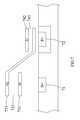
- FIG. 2shows an example of an optical sensing device according to an embodiment of the present invention.
- the optical sensing device 2comprises a substrate 21 , a first photodiode 22 , a second photodiode 23 , at least one first Fabry-Perot cavity 24 and at least one second Fabry-Perot cavity 25 .
- the first photodiode 22 and second photodiode 23are located on the substrate 21 .
- the substrate 21is a silicon substrate.
- the first Fabry-Perot cavity 24 or the second Fabry-Perot cavity 25are used for bandpass filtering the light with determined wavelength, for example, infrared light or recognizable light for human eyes.
- Each of the first Fabry-Perot cavity 24 and the second Fabry-Perot cavity 25has two reflective layers 241 , 242 and one interferometric layer 243 sandwiching between the two partially reflective layers 241 , 242 .
- the reflective layeris a silver thin film or an aluminum thin film.
- the interferometric layeris a silicon nitride thin film.
- FIG. 3shows an example of a Fabry-Perot cavity for filtering green light according to an embodiment of the present invention.
- the embodiment of Fabry-Perot cavity located on the a silicon substrate 31comprises a first silicon nitride (Si3N4: 3200 ⁇ 200) thin film layer 32 , a first silver (Ag: 285 ⁇ 35) partially reflective layer 33 , a second silicon nitride (Si3N4: 920 ⁇ 50) thin film layer 34 , a second silver (Ag: 285 ⁇ 35) reflective layer 35 , and a third silicon nitride (Si3N4: 3500 ⁇ 200) thin film layer 36 .
- Si3N4silicon nitride
- the preferred embodiment of the present inventionhas a P-type silicon substrate 31 which includes an array of N+ junction a photodiode element (not shown).
- the first silicon nitride (Si3N4: 3200 ⁇ 200) thin film layer 32is deposited on the silicon substrate 31
- the first silver (Ag: 285 ⁇ 35) partially reflective layer 33is deposited on the first silicon nitride thin film layer 32
- the second silicon nitride (Si3N4: 920 ⁇ 50) thin film layer 34is deposited on the first silver partially reflective layer 33
- the second silver (Ag: 285 ⁇ 35) partially reflective layer 35is deposited on the second silicon nitride thin film layer 34
- the third silicon nitride (Si3N4: 3500 ⁇ 200) thin film layer 36is deposited on the second silver partially reflective layer 35 .
- the single Fabry-Perot structurecan be made and constitutes a simple five layers process plus the photodetector silicon substrate 31 .
- the conventional all dielectric thin film photometric filtersrequire forty-two layers of thin-film coating.
- the first silicon nitride thin film layer 32is a bottom spacer layer
- the first silver partially reflective layer 33is a bottom partial reflector layer
- the second silicon nitride thin film layer 34is a center interferometric dielectric layer
- the second silver partially reflective layer 35is a top partial reflector layer
- the third silicon nitride thin film layer 36is a top moisture protective layer.
- the second silicon nitride thin film layer 34is a Fabry-Perot interferometric nitride layer, for filtering a certain spectral band of light, and a dielectric material such as silicon dioxide (SiO2) or oxy-nitride may be further applied thereon.
- the second silicon nitride thin film layer 34can be shaped by Plasma Enhanced Chemical Vapor Deposition (PECVD).
- PECVDPlasma Enhanced Chemical Vapor Deposition
- the first silver reflective layer 33 , the second silicon nitride thin film layer 34 , and the second silver reflective layer 35are formed the core of the Fabry-Perot optical cavity.
- the first silicon nitride thin film layer 32 and the third silicon nitride thin film layer 36are to protect the first silver reflective layer 33 and the second silver partially reflective layer 35 from moisture.
- the ambient light filter structurecan be made by the Complementary Metal Oxide Semiconductor (CMOS) technology, the bipolar technology, and the Bi-Complementary Metal Oxide Semiconductor (BiCMOS) technology. Furthermore, combining the single Fabry-Perot ambient light filter structure with a metal three light shield layer is to provide an effective stray light rejection structure for integrated electrical circuits (the metal three light shield layer is deposited between the silicon substrate).
- CMOSComplementary Metal Oxide Semiconductor
- BiCMOSBi-Complementary Metal Oxide Semiconductor
- the chartintroduces two responses, the first response 41 is the response of the ambient light filter structure according to the present invention and the second response 42 is that of the ideal human eye.
- the first response 41the wavelength spectrum ranging from 700 nm to 1100 nm is effectively blocked by the ambient light filter structure and the response of the ambient light filter structure is proximate to the response of the ideal human eye at the range of 400 nm to 700 nm.
- the peak wavelength of the ambient light filter structurelocates at around 555 nm 412 .
- the spectral response of the ambient light filter structuresubstantially matches the response of the human eye.
- FIG. 5shows a cross-sectional diagram of an optical sensing device with a multi-cavity Fabry-Perot ambient light color filter stack structure and a single-cavity Fabry-Perot UV filter stack structure according to an embodiment of the present invention.
- the multi-cavity Fabry-Perot ambient light color filter stack structureis deposited on a photodiode array element 54 which comprises three photodiodes 51 , 52 , 53 , such as the N+/P-substrate photodiodes shown in FIG. 5 .
- the multi-cavity Fabry-Perot ambient light color filter stack structurecomprises seven layers, they are: a first silver (Ag) partially reflective layer 511 deposited to cover the region of the first photodiode 51 ; a first silicon nitride (Si3N4) interferometric layer 512 deposited on the first silver partially reflective layer 511 ; a second silver (Ag) partially reflective layer 513 deposited the first silicon nitride interferometric layer 512 and the region of the second photodiode 52 ; a second silicon nitride (Si3N4) interferometric layer 521 deposited on the second silver partially reflective layer 513 to cover the region of the second photodiode 52 ; a third silver (Ag) partially reflective layer 522 deposited to cover both the second silicon nitride interferometric layer 521 and the region of the third photodiode 53 ; a third silicon nitride (Si3N4) interferometric layer 531 deposited
- the first silver partially reflective layer 511 , the first silicon nitride interferometric layer 512 , and the second silver partially reflective layer 513constitute a first Fabry-Perot optical cavity.
- the second silver partially reflective layer 513 , the second silicon nitride interferometric layer 521 , and the third silver partially reflective layer 522constitute a second Fabry-Perot optical cavity.
- the third silver partially reflective layer 522 , the third silicon nitride interferometric layer 531 , and the fourth silver partially reflective layer 532constitute a third Fabry-Perot optical cavity.
- the second silver partially reflective layer 513extends from the region of the first photodiode 51 to the region of the second photodiode 52 ; and the third silver partially reflective layer 522 extends from the region of the second photodiode 52 to the region of the third photodiode 53 .
- the second sliver partially reflective layer 513is a common Fabry-Perot reflector shared by the first photodiode 51 and the second photodiode 52 ; and the third silver partially reflective layer 522 is a common Fabry-Perot reflector shared by the second photodiode 52 and the third photodiode 53 .
- the multi-cavity Fabry-Perot ambient light color filter stack structurecan be made as a stair stack according to the present invention.
- the first silicon nitride interferometric layer 512 , the second silicon nitride interferometric layer 521 , and the third silicon nitride interferometric layer 531are the interferometric center dielectric layer of the ambient light color filter structure.
- the deposition thickness of each silicon nitride interferometric layermay be implemented using the modern thin film deposition equipment, such as the Plasma Enhanced Chemical Vapor Deposition, which is a well controlled thickness deposition process.
- the seven layers of the ambient light color filter stack structureare usually used for three-color system.
- the three-color systemis a three fundamental color separation that human eye can recognize such as red, green, and blue.
- the aforementioned region of the first photodiode 51may be implemented for capturing blue light, with a peak value near 450 nm in the wavelength spectrum.
- the aforementioned region of the second photodiode 52may be implemented for capturing green light with a peak value near 550 nm in the wavelength spectrum.
- the aforementioned region of the third photodiode 53may be implemented for capturing red light with a peak value near 650 nm in the wavelength spectrum.
- this type of seven layers of the ambient light color filter structureoffers a modular flexible filter stack solution (the modular Fabry-Perot filter cell is formed by two silver partially reflective layers plus a silicon nitride interferometric layer and the silicon nitride interferometric layer is placed between two silver component layers) for any additional color filtering and detection.
- Each additional color filter cellrequires only an extra modular Fabry-Perot filter stack masking layer and silicon nitride interferometric thickness layer deposition defines a specific optical passing spectrum.
- the partially reflective layersuch as silver deposition and mask photo patterning process is based on either lift-off or dry etching process to define the modular filter regions.
- the complementary colorincludes cyan, magenta, and yellow.
- the single-cavity Fabry-Perot UV filter stack structureis deposited on a photodiode 55 and comprises a first aluminum (Al) reflective layer 551 , a silicon nitride (Si3N4) interferometric layer 552 deposited on the first aluminum (Al) reflective layer 551 , and a second aluminum (Al) reflective layer 553 deposited on the silicon nitride interferometric layer 552 , and is capable of blocking the light that human eye can recognize. Therefore, photodiode 55 combined with such single-cavity Fabry-Perot UV filter stack structure can be a UV sensor.
- FIG. 6 and FIG. 7show examples of an optical sensing device having two single-cavity Fabry-Perot filter stack structures according to an embodiment of the present invention.
- two single-cavity Fabry-Perot filter stack structurescan share a reflective layer.
- FIG. 6 and FIG. 7show examples of an optical sensing device having two single-cavity Fabry-Perot filter stack structures according to an embodiment of the present invention.
- two single-cavity Fabry-Perot filter stack structurescan share a reflective layer.
- the aluminum (Al) reflective layer 631 , the silicon nitride thin film layer 632 , and the silver reflective layer 633are formed the core of the first Fabry-Perot optical cavity, and the aluminum reflective layer 641 , the silicon nitride thin film layer 642 , and the aluminum reflective layer 631 are formed the core of the second Fabry-Perot optical cavity, it means that the aluminum reflective layer 631 is shared by two single-cavity Fabry-Perot filter stack structures.
- the photodiode 61 combined with first Fabry-Perot optical cavitycan be functioned as an ambient sensor, and the photodiode 62 combined with second Fabry-Perot optical cavity can be functioned as a UV sensor.
- the aluminum (Al) reflective layer 731 , the silicon nitride thin film layer 732 , and the aluminum reflective layer 733are formed the core of the first Fabry-Perot optical cavity
- the aluminum reflective layer 733 , the silicon nitride thin film layer 741 , and the aluminum reflective layer 742are formed the core of the first Fabry-Perot optical cavity. Therefore, the photodiode 71 combined with first Fabry-Perot optical cavity can be functioned as an ambient sensor, and the photodiode 72 combined with second Fabry-Perot optical cavity can be functioned as a UV sensor.
- the present invention of multi-cavity Fabry-Perot filter stack filter structureis novel and useful and definite enhances the performance over the conventional CMOS polymer based RGB filter and further complies with the patent application requirements and is submitted to the Patent and Trademark Office for review and granting of the commensurate patent rights.
Landscapes
- Physics & Mathematics (AREA)
- General Physics & Mathematics (AREA)
- Optics & Photonics (AREA)
- Light Receiving Elements (AREA)
Abstract
Description
Claims (15)
Priority Applications (1)
| Application Number | Priority Date | Filing Date | Title |
|---|---|---|---|
| US12/379,720US8084728B2 (en) | 2005-07-06 | 2009-02-27 | Optical sensing device |
Applications Claiming Priority (2)
| Application Number | Priority Date | Filing Date | Title |
|---|---|---|---|
| US11/174,455US7521666B2 (en) | 2005-02-17 | 2005-07-06 | Multi-cavity Fabry-Perot ambient light filter apparatus |
| US12/379,720US8084728B2 (en) | 2005-07-06 | 2009-02-27 | Optical sensing device |
Related Parent Applications (1)
| Application Number | Title | Priority Date | Filing Date |
|---|---|---|---|
| US11/174,455Continuation-In-PartUS7521666B2 (en) | 2005-02-17 | 2005-07-06 | Multi-cavity Fabry-Perot ambient light filter apparatus |
Publications (2)
| Publication Number | Publication Date |
|---|---|
| US20090159785A1 US20090159785A1 (en) | 2009-06-25 |
| US8084728B2true US8084728B2 (en) | 2011-12-27 |
Family
ID=40787472
Family Applications (1)
| Application Number | Title | Priority Date | Filing Date |
|---|---|---|---|
| US12/379,720Active2026-08-01US8084728B2 (en) | 2005-07-06 | 2009-02-27 | Optical sensing device |
Country Status (1)
| Country | Link |
|---|---|
| US (1) | US8084728B2 (en) |
Cited By (28)
| Publication number | Priority date | Publication date | Assignee | Title |
|---|---|---|---|---|
| US20100308214A1 (en)* | 2009-06-04 | 2010-12-09 | Zena Technologies, Inc. | Array of nanowires in a single cavity with anti-reflective coating on substrate |
| US20130163005A1 (en)* | 2011-12-27 | 2013-06-27 | Capella Microsystems, Corp. | Optical Sensing Device |
| US8710488B2 (en) | 2009-12-08 | 2014-04-29 | Zena Technologies, Inc. | Nanowire structured photodiode with a surrounding epitaxially grown P or N layer |
| US8735797B2 (en) | 2009-12-08 | 2014-05-27 | Zena Technologies, Inc. | Nanowire photo-detector grown on a back-side illuminated image sensor |
| US8748799B2 (en) | 2010-12-14 | 2014-06-10 | Zena Technologies, Inc. | Full color single pixel including doublet or quadruplet si nanowires for image sensors |
| US8766272B2 (en) | 2009-12-08 | 2014-07-01 | Zena Technologies, Inc. | Active pixel sensor with nanowire structured photodetectors |
| US8791470B2 (en) | 2009-10-05 | 2014-07-29 | Zena Technologies, Inc. | Nano structured LEDs |
| US8810808B2 (en) | 2009-05-26 | 2014-08-19 | Zena Technologies, Inc. | Determination of optimal diameters for nanowires |
| EP2775275A1 (en) | 2013-03-08 | 2014-09-10 | Ams Ag | Ultraviolet semiconductor sensor device and method of measuring ultraviolet radiation |
| US8835831B2 (en) | 2010-06-22 | 2014-09-16 | Zena Technologies, Inc. | Polarized light detecting device and fabrication methods of the same |
| US8866065B2 (en) | 2010-12-13 | 2014-10-21 | Zena Technologies, Inc. | Nanowire arrays comprising fluorescent nanowires |
| US8890271B2 (en) | 2010-06-30 | 2014-11-18 | Zena Technologies, Inc. | Silicon nitride light pipes for image sensors |
| US8889455B2 (en) | 2009-12-08 | 2014-11-18 | Zena Technologies, Inc. | Manufacturing nanowire photo-detector grown on a back-side illuminated image sensor |
| US9000353B2 (en) | 2010-06-22 | 2015-04-07 | President And Fellows Of Harvard College | Light absorption and filtering properties of vertically oriented semiconductor nano wires |
| US9082673B2 (en) | 2009-10-05 | 2015-07-14 | Zena Technologies, Inc. | Passivated upstanding nanostructures and methods of making the same |
| US9299866B2 (en) | 2010-12-30 | 2016-03-29 | Zena Technologies, Inc. | Nanowire array based solar energy harvesting device |
| US9304035B2 (en) | 2008-09-04 | 2016-04-05 | Zena Technologies, Inc. | Vertical waveguides with various functionality on integrated circuits |
| US9343490B2 (en) | 2013-08-09 | 2016-05-17 | Zena Technologies, Inc. | Nanowire structured color filter arrays and fabrication method of the same |
| US9360364B2 (en) | 2014-05-30 | 2016-06-07 | Microsoft Technology Licensing, Llc | Sensory-and-logic system and method having ultraviolet light estimation from visible light |
| US9406709B2 (en) | 2010-06-22 | 2016-08-02 | President And Fellows Of Harvard College | Methods for fabricating and using nanowires |
| US9429723B2 (en) | 2008-09-04 | 2016-08-30 | Zena Technologies, Inc. | Optical waveguides in image sensors |
| US9478685B2 (en) | 2014-06-23 | 2016-10-25 | Zena Technologies, Inc. | Vertical pillar structured infrared detector and fabrication method for the same |
| US9515218B2 (en) | 2008-09-04 | 2016-12-06 | Zena Technologies, Inc. | Vertical pillar structured photovoltaic devices with mirrors and optical claddings |
| US20170236861A1 (en)* | 2016-02-12 | 2017-08-17 | Viavi Solutions Inc. | Optical filter array |
| US9923007B2 (en) | 2015-12-29 | 2018-03-20 | Viavi Solutions Inc. | Metal mirror based multispectral filter array |
| US9960199B2 (en) | 2015-12-29 | 2018-05-01 | Viavi Solutions Inc. | Dielectric mirror based multispectral filter array |
| US20230157061A1 (en)* | 2021-11-17 | 2023-05-18 | The Trustees Of Princeton University | Reconfigurable thin-film photonic filter banks for neuromorphic opto-electronic systems and methods |
| US11862648B2 (en) | 2018-03-30 | 2024-01-02 | Vishay Intertechnology, Inc. | Optoelectronic device arranged as a multi-spectral light sensor having a photodiode array with aligned light blocking layers and n-well regions |
Families Citing this family (11)
| Publication number | Priority date | Publication date | Assignee | Title |
|---|---|---|---|---|
| ES2345523B1 (en)* | 2008-07-18 | 2011-07-11 | Universidad Politécnica De Valencia | PROCEDURE AND APPLIANCE TO MEASURE THE EXTINCTION OF LIGHT IN WATER. |
| KR20110003696A (en)* | 2009-07-06 | 2011-01-13 | 삼성전자주식회사 | Optical filter array for single chip stereoscopic image sensor and manufacturing method thereof |
| US20150090909A1 (en)* | 2013-09-30 | 2015-04-02 | Capella Microsystems (Taiwan), Inc. | Selectable view angle optical sensor |
| US10078142B2 (en) | 2014-03-26 | 2018-09-18 | California Institute Of Technology | Sensor integrated metal dielectric filters for solar-blind silicon ultraviolet detectors |
| WO2016130582A1 (en)* | 2015-02-09 | 2016-08-18 | California Institute Of Technology | Sensor integrated metal dielectric filters for solar-blind silicon ultraviolet detectors |
| US9685575B2 (en) | 2015-03-06 | 2017-06-20 | Stmicroelectronics S.R.L. | Multiband double junction photodiode and related manufacturing process |
| US9865640B2 (en)* | 2016-01-31 | 2018-01-09 | Tower Semiconductor Ltd. | Backside illuminated (BSI) CMOS image sensor (CIS) with a resonant cavity and a method for manufacturing the BSI CIS |
| US12009379B2 (en)* | 2017-05-01 | 2024-06-11 | Visera Technologies Company Limited | Image sensor |
| US10670786B2 (en)* | 2018-04-13 | 2020-06-02 | Apple Inc. | Color ambient light sensor with tunable filter |
| EP3933461B1 (en)* | 2020-07-02 | 2025-03-19 | Samsung Electronics Co., Ltd. | Spectral filter, and image sensor and electronic device including the spectral filter |
| CN120341578B (en)* | 2025-06-11 | 2025-09-09 | 深圳大学 | Forward-backward switchable high-gain flat-top dual-mode switching Fabry-Perot cavity antenna |
Citations (1)
| Publication number | Priority date | Publication date | Assignee | Title |
|---|---|---|---|---|
| US20030179383A1 (en)* | 2002-03-21 | 2003-09-25 | Industrial Technology Research Institute | Fabry-perot filter apparatus with enhanced optical discrimination |
- 2009
- 2009-02-27USUS12/379,720patent/US8084728B2/enactiveActive
Patent Citations (1)
| Publication number | Priority date | Publication date | Assignee | Title |
|---|---|---|---|---|
| US20030179383A1 (en)* | 2002-03-21 | 2003-09-25 | Industrial Technology Research Institute | Fabry-perot filter apparatus with enhanced optical discrimination |
Cited By (50)
| Publication number | Priority date | Publication date | Assignee | Title |
|---|---|---|---|---|
| US9601529B2 (en) | 2008-09-04 | 2017-03-21 | Zena Technologies, Inc. | Light absorption and filtering properties of vertically oriented semiconductor nano wires |
| US9304035B2 (en) | 2008-09-04 | 2016-04-05 | Zena Technologies, Inc. | Vertical waveguides with various functionality on integrated circuits |
| US9515218B2 (en) | 2008-09-04 | 2016-12-06 | Zena Technologies, Inc. | Vertical pillar structured photovoltaic devices with mirrors and optical claddings |
| US9337220B2 (en) | 2008-09-04 | 2016-05-10 | Zena Technologies, Inc. | Solar blind ultra violet (UV) detector and fabrication methods of the same |
| US9410843B2 (en) | 2008-09-04 | 2016-08-09 | Zena Technologies, Inc. | Nanowire arrays comprising fluorescent nanowires and substrate |
| US9429723B2 (en) | 2008-09-04 | 2016-08-30 | Zena Technologies, Inc. | Optical waveguides in image sensors |
| US8810808B2 (en) | 2009-05-26 | 2014-08-19 | Zena Technologies, Inc. | Determination of optimal diameters for nanowires |
| US20100308214A1 (en)* | 2009-06-04 | 2010-12-09 | Zena Technologies, Inc. | Array of nanowires in a single cavity with anti-reflective coating on substrate |
| US8546742B2 (en)* | 2009-06-04 | 2013-10-01 | Zena Technologies, Inc. | Array of nanowires in a single cavity with anti-reflective coating on substrate |
| US9177985B2 (en) | 2009-06-04 | 2015-11-03 | Zena Technologies, Inc. | Array of nanowires in a single cavity with anti-reflective coating on substrate |
| US9082673B2 (en) | 2009-10-05 | 2015-07-14 | Zena Technologies, Inc. | Passivated upstanding nanostructures and methods of making the same |
| US8791470B2 (en) | 2009-10-05 | 2014-07-29 | Zena Technologies, Inc. | Nano structured LEDs |
| US9490283B2 (en) | 2009-11-19 | 2016-11-08 | Zena Technologies, Inc. | Active pixel sensor with nanowire structured photodetectors |
| US8766272B2 (en) | 2009-12-08 | 2014-07-01 | Zena Technologies, Inc. | Active pixel sensor with nanowire structured photodetectors |
| US8754359B2 (en) | 2009-12-08 | 2014-06-17 | Zena Technologies, Inc. | Nanowire photo-detector grown on a back-side illuminated image sensor |
| US8889455B2 (en) | 2009-12-08 | 2014-11-18 | Zena Technologies, Inc. | Manufacturing nanowire photo-detector grown on a back-side illuminated image sensor |
| US8735797B2 (en) | 2009-12-08 | 2014-05-27 | Zena Technologies, Inc. | Nanowire photo-detector grown on a back-side illuminated image sensor |
| US9263613B2 (en) | 2009-12-08 | 2016-02-16 | Zena Technologies, Inc. | Nanowire photo-detector grown on a back-side illuminated image sensor |
| US8710488B2 (en) | 2009-12-08 | 2014-04-29 | Zena Technologies, Inc. | Nanowire structured photodiode with a surrounding epitaxially grown P or N layer |
| US9123841B2 (en) | 2009-12-08 | 2015-09-01 | Zena Technologies, Inc. | Nanowire photo-detector grown on a back-side illuminated image sensor |
| US8835905B2 (en) | 2010-06-22 | 2014-09-16 | Zena Technologies, Inc. | Solar blind ultra violet (UV) detector and fabrication methods of the same |
| US9000353B2 (en) | 2010-06-22 | 2015-04-07 | President And Fellows Of Harvard College | Light absorption and filtering properties of vertically oriented semiconductor nano wires |
| US9054008B2 (en) | 2010-06-22 | 2015-06-09 | Zena Technologies, Inc. | Solar blind ultra violet (UV) detector and fabrication methods of the same |
| US9406709B2 (en) | 2010-06-22 | 2016-08-02 | President And Fellows Of Harvard College | Methods for fabricating and using nanowires |
| US8835831B2 (en) | 2010-06-22 | 2014-09-16 | Zena Technologies, Inc. | Polarized light detecting device and fabrication methods of the same |
| US8890271B2 (en) | 2010-06-30 | 2014-11-18 | Zena Technologies, Inc. | Silicon nitride light pipes for image sensors |
| US8866065B2 (en) | 2010-12-13 | 2014-10-21 | Zena Technologies, Inc. | Nanowire arrays comprising fluorescent nanowires |
| US8748799B2 (en) | 2010-12-14 | 2014-06-10 | Zena Technologies, Inc. | Full color single pixel including doublet or quadruplet si nanowires for image sensors |
| US9543458B2 (en) | 2010-12-14 | 2017-01-10 | Zena Technologies, Inc. | Full color single pixel including doublet or quadruplet Si nanowires for image sensors |
| US9299866B2 (en) | 2010-12-30 | 2016-03-29 | Zena Technologies, Inc. | Nanowire array based solar energy harvesting device |
| US20130163005A1 (en)* | 2011-12-27 | 2013-06-27 | Capella Microsystems, Corp. | Optical Sensing Device |
| US9683889B2 (en) | 2013-03-08 | 2017-06-20 | Ams Ag | Ultraviolet semiconductor sensor device and method of measuring ultraviolet radiation |
| EP2775275A1 (en) | 2013-03-08 | 2014-09-10 | Ams Ag | Ultraviolet semiconductor sensor device and method of measuring ultraviolet radiation |
| US9343490B2 (en) | 2013-08-09 | 2016-05-17 | Zena Technologies, Inc. | Nanowire structured color filter arrays and fabrication method of the same |
| US9360364B2 (en) | 2014-05-30 | 2016-06-07 | Microsoft Technology Licensing, Llc | Sensory-and-logic system and method having ultraviolet light estimation from visible light |
| US9478685B2 (en) | 2014-06-23 | 2016-10-25 | Zena Technologies, Inc. | Vertical pillar structured infrared detector and fabrication method for the same |
| US11450698B2 (en) | 2015-12-29 | 2022-09-20 | Viavi Solutions Inc. | Dielectric mirror based multispectral filter array |
| US9923007B2 (en) | 2015-12-29 | 2018-03-20 | Viavi Solutions Inc. | Metal mirror based multispectral filter array |
| US9960199B2 (en) | 2015-12-29 | 2018-05-01 | Viavi Solutions Inc. | Dielectric mirror based multispectral filter array |
| US12170300B2 (en) | 2015-12-29 | 2024-12-17 | Viavi Solutions Inc. | Metal mirror based multispectral filter array of optical sensor device |
| US10651216B2 (en) | 2015-12-29 | 2020-05-12 | Viavi Solutions Inc. | Metal mirror based multispectral filter array |
| US11670658B2 (en) | 2015-12-29 | 2023-06-06 | Viavi Solutions Inc. | Metal mirror based multispectral filter array |
| US11114485B2 (en) | 2015-12-29 | 2021-09-07 | Viavi Solutions Inc. | Metal mirror based multispectral filter array |
| US20170236861A1 (en)* | 2016-02-12 | 2017-08-17 | Viavi Solutions Inc. | Optical filter array |
| TWI788215B (en)* | 2016-02-12 | 2022-12-21 | 美商菲爾薇解析公司 | Optical filter array |
| US11049893B2 (en) | 2016-02-12 | 2021-06-29 | Viavi Solutions Inc. | Optical filter array |
| US10170509B2 (en)* | 2016-02-12 | 2019-01-01 | Viavi Solutions Inc. | Optical filter array |
| US12243887B2 (en) | 2016-02-12 | 2025-03-04 | Viavi Solutions Inc. | Optical filter array |
| US11862648B2 (en) | 2018-03-30 | 2024-01-02 | Vishay Intertechnology, Inc. | Optoelectronic device arranged as a multi-spectral light sensor having a photodiode array with aligned light blocking layers and n-well regions |
| US20230157061A1 (en)* | 2021-11-17 | 2023-05-18 | The Trustees Of Princeton University | Reconfigurable thin-film photonic filter banks for neuromorphic opto-electronic systems and methods |
Also Published As
| Publication number | Publication date |
|---|---|
| US20090159785A1 (en) | 2009-06-25 |
Similar Documents
| Publication | Publication Date | Title |
|---|---|---|
| US8084728B2 (en) | Optical sensing device | |
| US7521666B2 (en) | Multi-cavity Fabry-Perot ambient light filter apparatus | |
| US20130163005A1 (en) | Optical Sensing Device | |
| KR102200622B1 (en) | Fabricating a sensor device | |
| KR102292755B1 (en) | Induced transmission filter | |
| US12366692B2 (en) | Metal-dielectric optical filter, sensor device, and fabrication method | |
| US10222523B2 (en) | Sensor device including one or more metal-dielectric optical filters | |
| US8227883B2 (en) | Solid-state imaging device and camera | |
| CN110515149B (en) | Metal-dielectric filter, sensor device and manufacturing method | |
| US20080265349A1 (en) | Solid-State Image Sensor | |
| US20110032398A1 (en) | Image sensor with multilayer interference filters | |
| KR20170095158A (en) | Optical filter array | |
| US20230012033A1 (en) | Multi-bandpass optical interference filter | |
| JP2000180621A (en) | On-chip color filter and solid image pick-up element using the same | |
| TWI323481B (en) | Ambient light filter structure | |
| HK40043802A (en) | Induced transmission filter | |
| HK1243224A1 (en) | Method of fabricating a sensor device | |
| KR20030057676A (en) | Image sensor having notch filter | |
| HK40012097B (en) | Metal-dielectric optical filter, sensor device, and fabrication method | |
| HK40012097A (en) | Metal-dielectric optical filter, sensor device, and fabrication method |
Legal Events
| Date | Code | Title | Description |
|---|---|---|---|
| AS | Assignment | Owner name:CAPELLA MICROSYSTEMS CORP.,VIRGIN ISLANDS, BRITISH Free format text:ASSIGNMENT OF ASSIGNORS INTEREST;ASSIGNOR:TSANG, KOON-WING;REEL/FRAME:022391/0955 Effective date:20090219 Owner name:CAPELLA MICROSYSTEMS CORP., VIRGIN ISLANDS, BRITIS Free format text:ASSIGNMENT OF ASSIGNORS INTEREST;ASSIGNOR:TSANG, KOON-WING;REEL/FRAME:022391/0955 Effective date:20090219 | |
| STCF | Information on status: patent grant | Free format text:PATENTED CASE | |
| FPAY | Fee payment | Year of fee payment:4 | |
| AS | Assignment | Owner name:VISHAY CAPELLA MICROSYSTEMS (TAIWAN) LIMITED, TAIW Free format text:ASSIGNMENT OF ASSIGNORS INTEREST;ASSIGNOR:CAPELLA MICROSYSTEMS, CORP.;REEL/FRAME:037817/0771 Effective date:20160218 | |
| MAFP | Maintenance fee payment | Free format text:PAYMENT OF MAINTENANCE FEE, 8TH YR, SMALL ENTITY (ORIGINAL EVENT CODE: M2552); ENTITY STATUS OF PATENT OWNER: SMALL ENTITY Year of fee payment:8 | |
| MAFP | Maintenance fee payment | Free format text:PAYMENT OF MAINTENANCE FEE, 12TH YR, SMALL ENTITY (ORIGINAL EVENT CODE: M2553); ENTITY STATUS OF PATENT OWNER: SMALL ENTITY Year of fee payment:12 |