US8082672B2 - Mechanical patterning of thin film photovoltaic materials and structure - Google Patents
Mechanical patterning of thin film photovoltaic materials and structureDownload PDFInfo
- Publication number
- US8082672B2 US8082672B2US12/577,133US57713309AUS8082672B2US 8082672 B2US8082672 B2US 8082672B2US 57713309 AUS57713309 AUS 57713309AUS 8082672 B2US8082672 B2US 8082672B2
- Authority
- US
- United States
- Prior art keywords
- layer
- molybdenum
- tip
- absorber
- scribe device
- Prior art date
- Legal status (The legal status is an assumption and is not a legal conclusion. Google has not performed a legal analysis and makes no representation as to the accuracy of the status listed.)
- Expired - Fee Related
Links
- 239000000463materialSubstances0.000titleclaimsabstractdescription55
- 239000010409thin filmSubstances0.000titleclaimsabstractdescription24
- 238000000059patterningMethods0.000titledescription6
- 238000000034methodMethods0.000claimsabstractdescription63
- ZOKXTWBITQBERF-UHFFFAOYSA-NMolybdenumChemical compound[Mo]ZOKXTWBITQBERF-UHFFFAOYSA-N0.000claimsabstractdescription37
- 229910052750molybdenumInorganic materials0.000claimsabstractdescription37
- 239000011733molybdenumSubstances0.000claimsabstractdescription37
- 239000006096absorbing agentSubstances0.000claimsabstractdescription32
- 239000000758substrateSubstances0.000claimsabstractdescription22
- RYGMFSIKBFXOCR-UHFFFAOYSA-NCopperChemical group[Cu]RYGMFSIKBFXOCR-UHFFFAOYSA-N0.000claimsabstractdescription3
- 229910052793cadmiumInorganic materials0.000claimsabstractdescription3
- BDOSMKKIYDKNTQ-UHFFFAOYSA-Ncadmium atomChemical group[Cd]BDOSMKKIYDKNTQ-UHFFFAOYSA-N0.000claimsabstractdescription3
- 229910052802copperInorganic materials0.000claimsabstractdescription3
- 239000010949copperSubstances0.000claimsabstractdescription3
- HVMJUDPAXRRVQO-UHFFFAOYSA-Ncopper indiumChemical compound[Cu].[In]HVMJUDPAXRRVQO-UHFFFAOYSA-N0.000claimsdescription7
- 238000000151depositionMethods0.000claimsdescription5
- ZZEMEJKDTZOXOI-UHFFFAOYSA-Ndigallium;selenium(2-)Chemical compound[Ga+3].[Ga+3].[Se-2].[Se-2].[Se-2]ZZEMEJKDTZOXOI-UHFFFAOYSA-N0.000claimsdescription5
- 239000005361soda-lime glassSubstances0.000claimsdescription4
- WUPHOULIZUERAE-UHFFFAOYSA-N3-(oxolan-2-yl)propanoic acidChemical compoundOC(=O)CCC1CCCO1WUPHOULIZUERAE-UHFFFAOYSA-N0.000claimsdescription3
- 229910052980cadmium sulfideInorganic materials0.000claimsdescription3
- KTSFMFGEAAANTF-UHFFFAOYSA-N[Cu].[Se].[Se].[In]Chemical compound[Cu].[Se].[Se].[In]KTSFMFGEAAANTF-UHFFFAOYSA-N0.000claimsdescription2
- 230000015572biosynthetic processEffects0.000claimsdescription2
- 229910003460diamondInorganic materials0.000claimsdescription2
- 239000010432diamondSubstances0.000claimsdescription2
- HBMJWWWQQXIZIP-UHFFFAOYSA-Nsilicon carbideChemical compound[Si+]#[C-]HBMJWWWQQXIZIP-UHFFFAOYSA-N0.000claimsdescription2
- 229910010271silicon carbideInorganic materials0.000claimsdescription2
- UONOETXJSWQNOL-UHFFFAOYSA-Ntungsten carbideChemical compound[W+]#[C-]UONOETXJSWQNOL-UHFFFAOYSA-N0.000claimsdescription2
- 239000000203mixtureSubstances0.000claims1
- 238000012986modificationMethods0.000description11
- 230000004048modificationEffects0.000description11
- 238000004519manufacturing processMethods0.000description10
- 230000004888barrier functionEffects0.000description6
- 238000010586diagramMethods0.000description6
- 239000004065semiconductorSubstances0.000description5
- 238000004544sputter depositionMethods0.000description5
- 239000002178crystalline materialSubstances0.000description4
- 238000005516engineering processMethods0.000description4
- 229910052751metalInorganic materials0.000description4
- 239000002184metalSubstances0.000description4
- 230000008901benefitEffects0.000description3
- 230000005670electromagnetic radiationEffects0.000description3
- 239000010408filmSubstances0.000description3
- 239000000446fuelSubstances0.000description3
- 239000011521glassSubstances0.000description3
- 239000007769metal materialSubstances0.000description3
- VYPSYNLAJGMNEJ-UHFFFAOYSA-Nsilicon dioxideInorganic materialsO=[Si]=OVYPSYNLAJGMNEJ-UHFFFAOYSA-N0.000description3
- 239000002028BiomassSubstances0.000description2
- BWGNESOTFCXPMA-UHFFFAOYSA-NDihydrogen disulfideChemical compoundSSBWGNESOTFCXPMA-UHFFFAOYSA-N0.000description2
- YCKRFDGAMUMZLT-UHFFFAOYSA-NFluorine atomChemical compound[F]YCKRFDGAMUMZLT-UHFFFAOYSA-N0.000description2
- ATUOYWHBWRKTHZ-UHFFFAOYSA-NPropaneChemical compoundCCCATUOYWHBWRKTHZ-UHFFFAOYSA-N0.000description2
- 150000004770chalcogenidesChemical class0.000description2
- 238000005229chemical vapour depositionMethods0.000description2
- 239000000356contaminantSubstances0.000description2
- 230000008021depositionEffects0.000description2
- 239000007772electrode materialSubstances0.000description2
- 230000008020evaporationEffects0.000description2
- 238000001704evaporationMethods0.000description2
- 239000011737fluorineSubstances0.000description2
- 229910052731fluorineInorganic materials0.000description2
- 238000009432framingMethods0.000description2
- AMGQUBHHOARCQH-UHFFFAOYSA-Nindium;oxotinChemical compound[In].[Sn]=OAMGQUBHHOARCQH-UHFFFAOYSA-N0.000description2
- 239000002245particleSubstances0.000description2
- 238000005240physical vapour depositionMethods0.000description2
- 238000007747platingMethods0.000description2
- XOLBLPGZBRYERU-UHFFFAOYSA-Ntin dioxideChemical compoundO=[Sn]=OXOLBLPGZBRYERU-UHFFFAOYSA-N0.000description2
- 229910001887tin oxideInorganic materials0.000description2
- PFNQVRZLDWYSCW-UHFFFAOYSA-N(fluoren-9-ylideneamino) n-naphthalen-1-ylcarbamateChemical compoundC12=CC=CC=C2C2=CC=CC=C2C1=NOC(=O)NC1=CC=CC2=CC=CC=C12PFNQVRZLDWYSCW-UHFFFAOYSA-N0.000description1
- ZOXJGFHDIHLPTG-UHFFFAOYSA-NBoronChemical compound[B]ZOXJGFHDIHLPTG-UHFFFAOYSA-N0.000description1
- QPLDLSVMHZLSFG-UHFFFAOYSA-NCuOInorganic materials[Cu]=OQPLDLSVMHZLSFG-UHFFFAOYSA-N0.000description1
- MBMLMWLHJBBADN-UHFFFAOYSA-NFerrous sulfideChemical compound[Fe]=SMBMLMWLHJBBADN-UHFFFAOYSA-N0.000description1
- GYHNNYVSQQEPJS-UHFFFAOYSA-NGalliumChemical compound[Ga]GYHNNYVSQQEPJS-UHFFFAOYSA-N0.000description1
- 229910052581Si3N4Inorganic materials0.000description1
- XUIMIQQOPSSXEZ-UHFFFAOYSA-NSiliconChemical compound[Si]XUIMIQQOPSSXEZ-UHFFFAOYSA-N0.000description1
- NRTOMJZYCJJWKI-UHFFFAOYSA-NTitanium nitrideChemical compound[Ti]#NNRTOMJZYCJJWKI-UHFFFAOYSA-N0.000description1
- 229910052782aluminiumInorganic materials0.000description1
- XAGFODPZIPBFFR-UHFFFAOYSA-NaluminiumChemical compound[Al]XAGFODPZIPBFFR-UHFFFAOYSA-N0.000description1
- 229910052796boronInorganic materials0.000description1
- 239000001273butaneSubstances0.000description1
- 238000006243chemical reactionMethods0.000description1
- 238000000224chemical solution depositionMethods0.000description1
- 239000003245coalSubstances0.000description1
- 230000006835compressionEffects0.000description1
- 238000007906compressionMethods0.000description1
- 238000004590computer programMethods0.000description1
- 239000004020conductorSubstances0.000description1
- 238000010411cookingMethods0.000description1
- BERDEBHAJNAUOM-UHFFFAOYSA-Ncopper(I) oxideInorganic materials[Cu]O[Cu]BERDEBHAJNAUOM-UHFFFAOYSA-N0.000description1
- OMZSGWSJDCOLKM-UHFFFAOYSA-Ncopper(II) sulfideChemical compound[S-2].[Cu+2]OMZSGWSJDCOLKM-UHFFFAOYSA-N0.000description1
- KRFJLUBVMFXRPN-UHFFFAOYSA-Ncuprous oxideChemical compound[O-2].[Cu+].[Cu+]KRFJLUBVMFXRPN-UHFFFAOYSA-N0.000description1
- 239000003989dielectric materialSubstances0.000description1
- 239000002019doping agentSubstances0.000description1
- 230000005611electricityEffects0.000description1
- 230000007613environmental effectEffects0.000description1
- 239000005350fused silica glassSubstances0.000description1
- 229910052733galliumInorganic materials0.000description1
- 239000003502gasolineSubstances0.000description1
- UQSXHKLRYXJYBZ-UHFFFAOYSA-Niron oxideInorganic materials[Fe]=OUQSXHKLRYXJYBZ-UHFFFAOYSA-N0.000description1
- JEIPFZHSYJVQDO-UHFFFAOYSA-Niron(III) oxideInorganic materialsO=[Fe]O[Fe]=OJEIPFZHSYJVQDO-UHFFFAOYSA-N0.000description1
- 238000003475laminationMethods0.000description1
- 229910044991metal oxideInorganic materials0.000description1
- 150000004706metal oxidesChemical class0.000description1
- 229910052976metal sulfideInorganic materials0.000description1
- IJDNQMDRQITEOD-UHFFFAOYSA-Nn-butaneChemical compoundCCCCIJDNQMDRQITEOD-UHFFFAOYSA-N0.000description1
- OFBQJSOFQDEBGM-UHFFFAOYSA-Nn-pentaneNatural productsCCCCCOFBQJSOFQDEBGM-UHFFFAOYSA-N0.000description1
- 239000003921oilSubstances0.000description1
- 230000005693optoelectronicsEffects0.000description1
- TWNQGVIAIRXVLR-UHFFFAOYSA-Noxo(oxoalumanyloxy)alumaneChemical compoundO=[Al]O[Al]=OTWNQGVIAIRXVLR-UHFFFAOYSA-N0.000description1
- BPUBBGLMJRNUCC-UHFFFAOYSA-Noxygen(2-);tantalum(5+)Chemical compound[O-2].[O-2].[O-2].[O-2].[O-2].[Ta+5].[Ta+5]BPUBBGLMJRNUCC-UHFFFAOYSA-N0.000description1
- RVTZCBVAJQQJTK-UHFFFAOYSA-Noxygen(2-);zirconium(4+)Chemical compound[O-2].[O-2].[Zr+4]RVTZCBVAJQQJTK-UHFFFAOYSA-N0.000description1
- 239000003348petrochemical agentSubstances0.000description1
- 239000003209petroleum derivativeSubstances0.000description1
- 239000001294propaneSubstances0.000description1
- 239000010453quartzSubstances0.000description1
- 238000012827research and developmentMethods0.000description1
- 238000007789sealingMethods0.000description1
- 150000004771selenidesChemical class0.000description1
- 229910052710siliconInorganic materials0.000description1
- 239000010703siliconSubstances0.000description1
- HQVNEWCFYHHQES-UHFFFAOYSA-Nsilicon nitrideChemical compoundN12[Si]34N5[Si]62N3[Si]51N64HQVNEWCFYHHQES-UHFFFAOYSA-N0.000description1
- 229910052814silicon oxideInorganic materials0.000description1
- 229910001415sodium ionInorganic materials0.000description1
- 230000008022sublimationEffects0.000description1
- 238000000859sublimationMethods0.000description1
- 238000005987sulfurization reactionMethods0.000description1
- 229910001936tantalum oxideInorganic materials0.000description1
- 238000007738vacuum evaporationMethods0.000description1
- XLYOFNOQVPJJNP-UHFFFAOYSA-NwaterSubstancesOXLYOFNOQVPJJNP-UHFFFAOYSA-N0.000description1
- 239000002023woodSubstances0.000description1
- XLOMVQKBTHCTTD-UHFFFAOYSA-Nzinc oxideInorganic materials[Zn]=OXLOMVQKBTHCTTD-UHFFFAOYSA-N0.000description1
- 229910001928zirconium oxideInorganic materials0.000description1
Images


Classifications
- H—ELECTRICITY
- H10—SEMICONDUCTOR DEVICES; ELECTRIC SOLID-STATE DEVICES NOT OTHERWISE PROVIDED FOR
- H10F—INORGANIC SEMICONDUCTOR DEVICES SENSITIVE TO INFRARED RADIATION, LIGHT, ELECTROMAGNETIC RADIATION OF SHORTER WAVELENGTH OR CORPUSCULAR RADIATION
- H10F71/00—Manufacture or treatment of devices covered by this subclass
- H—ELECTRICITY
- H10—SEMICONDUCTOR DEVICES; ELECTRIC SOLID-STATE DEVICES NOT OTHERWISE PROVIDED FOR
- H10F—INORGANIC SEMICONDUCTOR DEVICES SENSITIVE TO INFRARED RADIATION, LIGHT, ELECTROMAGNETIC RADIATION OF SHORTER WAVELENGTH OR CORPUSCULAR RADIATION
- H10F10/00—Individual photovoltaic cells, e.g. solar cells
- H10F10/10—Individual photovoltaic cells, e.g. solar cells having potential barriers
- H10F10/16—Photovoltaic cells having only PN heterojunction potential barriers
- H10F10/167—Photovoltaic cells having only PN heterojunction potential barriers comprising Group I-III-VI materials, e.g. CdS/CuInSe2 [CIS] heterojunction photovoltaic cells
- H—ELECTRICITY
- H10—SEMICONDUCTOR DEVICES; ELECTRIC SOLID-STATE DEVICES NOT OTHERWISE PROVIDED FOR
- H10F—INORGANIC SEMICONDUCTOR DEVICES SENSITIVE TO INFRARED RADIATION, LIGHT, ELECTROMAGNETIC RADIATION OF SHORTER WAVELENGTH OR CORPUSCULAR RADIATION
- H10F19/00—Integrated devices, or assemblies of multiple devices, comprising at least one photovoltaic cell covered by group H10F10/00, e.g. photovoltaic modules
- H10F19/30—Integrated devices, or assemblies of multiple devices, comprising at least one photovoltaic cell covered by group H10F10/00, e.g. photovoltaic modules comprising thin-film photovoltaic cells
- H10F19/31—Integrated devices, or assemblies of multiple devices, comprising at least one photovoltaic cell covered by group H10F10/00, e.g. photovoltaic modules comprising thin-film photovoltaic cells having multiple laterally adjacent thin-film photovoltaic cells deposited on the same substrate
- Y—GENERAL TAGGING OF NEW TECHNOLOGICAL DEVELOPMENTS; GENERAL TAGGING OF CROSS-SECTIONAL TECHNOLOGIES SPANNING OVER SEVERAL SECTIONS OF THE IPC; TECHNICAL SUBJECTS COVERED BY FORMER USPC CROSS-REFERENCE ART COLLECTIONS [XRACs] AND DIGESTS
- Y02—TECHNOLOGIES OR APPLICATIONS FOR MITIGATION OR ADAPTATION AGAINST CLIMATE CHANGE
- Y02E—REDUCTION OF GREENHOUSE GAS [GHG] EMISSIONS, RELATED TO ENERGY GENERATION, TRANSMISSION OR DISTRIBUTION
- Y02E10/00—Energy generation through renewable energy sources
- Y02E10/50—Photovoltaic [PV] energy
- Y02E10/541—CuInSe2 material PV cells
Definitions
- the present inventionrelates generally to photovoltaic materials and manufacturing method. More particularly, the present invention provides a method and structure for fabricating a thin film solar cells.
- the present method and structureinclude a patterned thin film stack layer for manufacture of copper indium gallium diselenide based thin film photovoltaic devices, but it would be recognized that the invention may have other configurations.
- Petrochemical energyincludes gas and oil.
- Gasincludes lighter forms such as butane and propane, commonly used to heat homes and serve as fuel for cooking
- Gasalso includes gasoline, diesel, and jet fuel, commonly used for transportation purposes. Heavier forms of petrochemicals can also be used to heat homes in some places.
- the supply of petrochemical fuelis limited and essentially fixed based upon the amount available on the planet Earth. Additionally, as more people use petroleum products in growing amounts, it is rapidly becoming a scarce resource, which will eventually become depleted over time.
- hydroelectric poweris derived from electric generators driven by the flow of water produced by dams such as the Hoover Dam in Nevada. The electric power generated is used to power a large portion of the city of Los Angeles in California. Clean and renewable sources of energy also include wind, waves, biomass, and the like. That is, windmills convert wind energy into more useful forms of energy such as electricity. Still other types of clean energy include solar energy. Specific details of solar energy can be found throughout the present background and more particularly below.
- Solar energy technologygenerally converts electromagnetic radiation from the sun to other useful forms of energy. These other forms of energy include thermal energy and electrical power.
- solar cellsare often used. Although solar energy is environmentally clean and has been successful to a point, many limitations remain to be resolved before it becomes widely used throughout the world.
- one type of solar celluses crystalline materials, which are derived from semiconductor material ingots. These crystalline materials can be used to fabricate optoelectronic devices that include photovoltaic and photodiode devices that convert electromagnetic radiation into electrical power.
- crystalline materialsare often costly and difficult to make on a large scale. Additionally, devices made from such crystalline materials often have low energy conversion efficiencies.
- Embodiments according to the present inventionrelates to photovoltaic materials and manufacturing method. More particularly, the present invention provides a method and structure for fabricating a thin film solar cells. Merely by way of example, the present method and structure provides a patterned thin film stack layer for manufacture of copper indium gallium diselenide based thin film photovoltaic devices, but it would be recognized that the invention may have other configurations.
- a method for forming one or more patterns for a thin film photovoltaic materialincludes providing a substrate including a molybdenum layer and an overlying absorber layer and a window layer.
- the overlying absorbercomprises a copper bearing species and the window layer comprises a cadmium bearing species.
- the methodsupports the substrate to expose a surface of the window layer.
- the methoduses a scribe device including a scribe having a tip.
- the scribe deviceis configured to pivot about one or more regions and to apply pressure to the tip, such that the tip is placed on a selected region of the window layer.
- the scribe deviceis allowed to pattern at least the window layer while stopping on the molybdenum layer at a determined speed in a specific embodiment.
- the tipmay form a slight pattern without causing an “open” in the molybdenum layer.
- the methodprovides a method for patterning a window layer together with an absorber layer to form a photovoltaic cell in a specific embodiment.
- the present methodprovides a clean scribe region free of particles and contaminants on an underlying electrode layer, for example, a molybdenum layer.
- the resulting photovoltaic cellhas a desirable contact resistance characteristics in a preferred embodiment.
- the present methoduses conventional process equipment without major modifications to provide for a cost effective way to fabricate a photovoltaic cell in a specific embodiment.
- one or more of these benefitsmay be achieved.
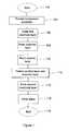
- FIG. 1is a simplified process flow diagram illustrating a method of fabricating a photovoltaic cell according to an embodiment of the present invention.
- FIG. 2-7are simplified diagrams illustrating a method of fabricating a photovoltaic cell according to an embodiment of the present invention.
- Embodiments according to the present inventionrelates to photovoltaic materials and manufacturing method. More particularly, the present invention provides a method and structure for fabricating a thin film solar cells. Merely by way of example, the present method and structure provide a patterned thin film stack layer for manufacture of copper indium gallium diselenide based thin film photovoltaic devices, but it would be recognized that the invention may have other configurations.
- FIG. 1is a simplified process flow diagram illustrating a method for fabricating a thin film photovoltaic cell according to an embodiment of the present invention.
- the methodbegins with a Start step (Step 102 ).
- the methodincludes providing a transparent substrate (Step 104 ) having a first surface region.
- the transparent substratecan be a soda lime glass in a specific embodiment.
- a first electrode layeris formed overlying the first surface region of the transparent substrate (Step 106 ).
- the first electrode layercan be provided using a molybdenum material in a specific embodiment.
- Other electrode materialssuch as transparent conductive oxide material, other metal materials may also be used, depending on the application.
- the methodincludes forming an absorber layer overlying the first electrode layer (Step 108 ) and forming a window layer overlying the absorber layer (Step 110 ).
- the window layer and the absorber layeris patterned using a scribe device (Step 112 ).
- a second electrode layeris formed overlying the window layer (Step 114 ).
- the methodperforms other steps to complete the photovoltaic device (Step 116 ). These other steps may include providing interconnect elements, ribbon elements, lamination, framing among others to complete the photovoltaic device.
- the methodends with an end step (Step 118 ). Of course there can be other variations, modifications, and alternatives.
- the above sequence of stepsprovides a method of forming a photovoltaic device according to an embodiment of the present invention.
- the methodincludes a step of patterning an absorber layer and a window layer using a scribe device according to a specific embodiment.
- one or more stepsmay be added, one or more steps may be eliminated, and one or more steps may be performed in a different sequence without departing from the scope of the claims herein.
- One skilled in the artwould recognize other variations, modifications, and alternatives.
- FIGS. 2-6are simplified diagrams illustrating a method of fabricating a photovoltaic cell according to an embodiment of the present invention. These diagrams are merely examples and should not unduly limit the claims herein. One skilled in the art would recognize other variations, modifications, and alternatives.
- a transparent substrate member 202 including a surface region 204is provided.
- the substrate membercan be a glass material such as soda lime glass in certain embodiment. Soda lime glass is a cost effective option for the transparent substrate member. Other suitable transparent substrates such as quartz, fused silica, solar glass can also be used.
- Each of the transparent substratecan include a barrier layer deposited on a surface region.
- the barrier layerprevents sodium ions from the glass material to diffuse into photovoltaic material area in a specific embodiment.
- the barrier layercan be a dielectric material such as silicon oxide deposited using technique such as a sputtering process, a chemical vapor deposition process, including plasma enhanced processes, and others. Other barrier materials may also be used. These barrier materials include aluminum oxide, titanium nitride, silicon nitride, tantalum oxide, zirconium oxide depending on the embodiment.
- the methodincludes forming a first electrode layer 302 overlying the surface region of the transparent substrate member which can have a barrier layer formed thereon.
- the first electrode layermay be provided using a transparent conductor oxide (TCO) such as indium tin oxide (commonly called ITO), fluorine doped tin oxide, and the like.
- TCOtransparent conductor oxide
- ITOindium tin oxide
- fluorine doped tin oxideand the like.
- the first electrode layermay be provided using a metal material.
- the metal materialcan be a molybdenum material in a specific embodiment.
- the molybdenum materialcan be formed using deposition techniques such as sputtering, plating, physical vapor deposition (including evaporation, sublimation), chemical vapor deposition (including plasma enhanced processes) following by a patterning process.
- Molybdenum materialprovides certain advantage over other electrode material for a CIG or CIGS based thin film photovoltaic cells.
- molybdenum materialprovides a low contact resistance for CIGS film and stability over subsequent process steps.
- molybdenum materialis formed by depositing a first molybdenum layer overlying the transparent substrate member.
- the first molybdenum layerhas a first thickness and a tensile characteristics in a specific embodiment.
- a second molybdenum layer having a compression characteristics and a second thicknessis formed overlying the first molybdenum layer.
- the first electrode layer comprising the molybdenum materialcan be further patterned as shown.
- the methodincludes forming an absorber layer 402 overlying a surface region of the first electrode layer.
- the absorber layercan be a thin film semiconductor material in a specific embodiment.
- the thin film semiconductor materialis a p-type semiconductor material provided by a copper indium disulfide material, or a copper indium gallium disulfide material, or a copper indium diselenide material, or a copper indium gallium diselenide material, any combination of these, or others, depending on the application.
- the p-type characteristicsmay be provided using dopants such as boron or aluminum species.
- the absorber layermay be deposited by techniques such as sputtering, plating, evaporation including a sulfurization or selenization step. Further details of the formation of the absorber material may be found in Provisional U.S. Patent Application No. 61/059,253, titled “High Efficiency Photovoltaic Cell and Manufacturing Method,” commonly assigned, and hereby incorporated by reference.
- the methodforms a window layer 502 overlying a surface region of the absorber layer to form a photovoltaic film stack to provide for a pn junction for the photovoltaic cell.
- the window layeris often provided using a wide bandgap n-type semiconductor material for a p-type absorber layer in a specific embodiment.
- the window layeruses a cadmium sulfide material for a photovoltaic cell using CIGS, CIS and related materials as absorber layer.
- the window layercan be deposited using techniques such as sputtering, vacuum evaporation, chemical bath deposition, among others.
- the methodincludes patterning the absorber layer and the window layer as shown in FIG. 6 .
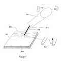
- a substrate 602is provided.
- the substrateincludes a molybdenum layer overlying a transparent substrate and an overlying absorber layer.
- the absorber layercomprises a CIGS thin film material in a specific embodiment.
- a window layercomprising a cadmium sulfide overlies the absorber layer to provide for a photovoltaic stack material.
- the substrateis provided on a supporting tray or a rack 604 , exposing the window layer.
- the photovoltaic stack materialis characterized by a brittle nature and molybdenum is a relatively hard metal.
- the methodincludes providing a scribe device 606 .
- the tipcan be made of material such as diamond, tungsten carbide, or silicon carbide, and the like. Other materials having sufficient hardness may also be used for the tip depending on the application.
- the tipis characterized by a radius 620 ranging from about 20 microns to about 40 microns and preferably 25 microns and more.
- the scribe deviceincludes a scribe head 614 which can be a pivot device in a specific embodiment. In a specific embodiment, the scribe device is configured to pivot about one or more regions on the scribe head. As shown, the scribe device includes a pressure device 618 to dial in a force to maintain the tip on the surface of the window layer while the scribe device moves along the surface of the window layer.
- the pressure devicecan be a pressure-spring, a weight, or the like in a specific embodiment.
- the tipis configured to be at an angle 610 to a normal to a surface region 612 of the window layer.
- the anglecan be ranging from about zero degrees to about 40 degrees and preferably between 10 degrees and 20 degrees depending on the embodiment.
- the tipis configured to be at an angle of about 15 degrees to the normal to the surface.
- the methodincludes allowing the scribe device to move over a selected region in one or more passes to remove the photovoltaic stack material from the selected region to form a scribe region.
- the scribe devicesubstantially stops at the underlying molybdenum surface.
- a simplified cross sectional diagram illustrating a scribe region 702 provided by the scribe deviceis shown in FIG. 7 .
- the molybdenum layerincludes an interface layer 704 formed from the absorber layer material and the molybdenum material.
- the interface layercomprises a graded material characterized by a MoSe x , species or a MoS y species depending on the absorber material used.
- the graded materialcan have a thickness of about 100 Angstroms in a specific embodiment.
- the scribe regionextends through a thickness 706 of the photovoltaic material stack and the interface layer forming a recess region of no greater than 200 Angstroms in the molybdenum layer in a preferred embodiment.
- the selected regionallows the photovoltaic stack material to be aligned with underlying molybdenum layer, which has been patterned.
- the selected regionforms a pattern having a width 708 ranging from about 30 microns to about 100 microns in a specific embodiment. In a specific embodiment, the pattern can have a width of about 50 microns.
- the one or more passesallows the scribe region to be substantially cleaned and free of contaminants and particles thus providing a lower contact resistivity and good ohmic contact to interconnects for the photovoltaic cell in a specific embodiment.
- the scribe regionseparates a first photovoltaic region from a second photovoltaic region without shorting in a preferred embodiment.
- the scribe devicemoves at a predetermined optimized speed at about 0.25 meter per second and greater, or may be slightly less. Of course there can be other variations, modifications, and alternatives.
- the methodperforms other steps to complete the photovoltaic cell. These other steps can include forming a second electrode layer overlying the window layer, sealing the photovoltaic cell, framing, among others.
- the second electrode layercan be a transparent conductive oxide such as indium tin oxide (commonly called ITO), fluorine doped tin oxide, and the like.
- ITOindium tin oxide
- the second electrode layercan be deposited using techniques such as sputtering, physical vapor deposition, solution based deposition, and others. Of course there can be other variations, modifications, and alternatives.
- Examples of these other thin film photovoltaic materialsmay include metal chalcogenide materials.
- metal chalcogenide materialscan include metal oxides (for example, ZnO, FeO, Fe 2 O 3 , CuO, Cu 2 O), metal sulfides (for example, iron sulfide, copper sulfide) metal selenides (for example, zinc selenide), and others.
- the present methodcan also be applied to silicon based photovoltaic devices.
- one of ordinary skill in the artwould recognize other variations, modifications and alternatives.
Landscapes
- Photovoltaic Devices (AREA)
Abstract
Description
Claims (15)
Priority Applications (1)
| Application Number | Priority Date | Filing Date | Title |
|---|---|---|---|
| US12/577,133US8082672B2 (en) | 2008-10-17 | 2009-10-09 | Mechanical patterning of thin film photovoltaic materials and structure |
Applications Claiming Priority (2)
| Application Number | Priority Date | Filing Date | Title |
|---|---|---|---|
| US10650608P | 2008-10-17 | 2008-10-17 | |
| US12/577,133US8082672B2 (en) | 2008-10-17 | 2009-10-09 | Mechanical patterning of thin film photovoltaic materials and structure |
Publications (2)
| Publication Number | Publication Date |
|---|---|
| US20110020977A1 US20110020977A1 (en) | 2011-01-27 |
| US8082672B2true US8082672B2 (en) | 2011-12-27 |
Family
ID=43497666
Family Applications (1)
| Application Number | Title | Priority Date | Filing Date |
|---|---|---|---|
| US12/577,133Expired - Fee RelatedUS8082672B2 (en) | 2008-10-17 | 2009-10-09 | Mechanical patterning of thin film photovoltaic materials and structure |
Country Status (1)
| Country | Link |
|---|---|
| US (1) | US8082672B2 (en) |
Citations (19)
| Publication number | Priority date | Publication date | Assignee | Title |
|---|---|---|---|---|
| US4502225A (en)* | 1983-05-06 | 1985-03-05 | Rca Corporation | Mechanical scriber for semiconductor devices |
| US4996108A (en) | 1989-01-17 | 1991-02-26 | Simon Fraser University | Sheets of transition metal dichalcogenides |
| US5125984A (en) | 1990-05-31 | 1992-06-30 | Siemens Aktiengesellschaft | Induced junction chalcopyrite solar cell |
| US5261968A (en) | 1992-01-13 | 1993-11-16 | Photon Energy, Inc. | Photovoltaic cell and method |
| US5501744A (en) | 1992-01-13 | 1996-03-26 | Photon Energy, Inc. | Photovoltaic cell having a p-type polycrystalline layer with large crystals |
| US5536333A (en) | 1992-05-12 | 1996-07-16 | Solar Cells, Inc. | Process for making photovoltaic devices and resultant product |
| US5665175A (en) | 1990-05-30 | 1997-09-09 | Safir; Yakov | Bifacial solar cell |
| US5855974A (en)* | 1993-10-25 | 1999-01-05 | Ford Global Technologies, Inc. | Method of producing CVD diamond coated scribing wheels |
| US6134049A (en)* | 1998-09-25 | 2000-10-17 | The Regents Of The University Of California | Method to adjust multilayer film stress induced deformation of optics |
| US6328871B1 (en) | 1999-08-16 | 2001-12-11 | Applied Materials, Inc. | Barrier layer for electroplating processes |
| US20050223570A1 (en)* | 2002-09-26 | 2005-10-13 | Honda Giken Kogyo Kabushiki Kaisha | Mechanical scribing apparatus with controlling force of a scribing cutter |
| US20060220059A1 (en) | 2003-04-09 | 2006-10-05 | Matsushita Electric Industrial Co., Ltd | Solar cell |
| US20070089782A1 (en) | 2003-10-02 | 2007-04-26 | Scheuten Glasgroep | Spherical or grain-shaped semiconductor element for use in solar cells and method for producing the same; method for producing a solar cell comprising said semiconductor element and solar cell |
| US20070151596A1 (en) | 2004-02-20 | 2007-07-05 | Sharp Kabushiki Kaisha | Substrate for photoelectric conversion device, photoelectric conversion device, and stacked photoelectric conversion device |
| US20070169810A1 (en) | 2004-02-19 | 2007-07-26 | Nanosolar, Inc. | High-throughput printing of semiconductor precursor layer by use of chalcogen-containing vapor |
| US20080041446A1 (en) | 2006-08-09 | 2008-02-21 | Industrial Technology Research Institute | Dye-sensitized solar cells and method for fabricating same |
| US20080092945A1 (en) | 2006-10-24 | 2008-04-24 | Applied Quantum Technology Llc | Semiconductor Grain and Oxide Layer for Photovoltaic Cells |
| US20080092953A1 (en) | 2006-05-15 | 2008-04-24 | Stion Corporation | Method and structure for thin film photovoltaic materials using bulk semiconductor materials |
| US20080216886A1 (en)* | 2005-07-01 | 2008-09-11 | Tadashi Iwakura | Solar Cell Module |
- 2009
- 2009-10-09USUS12/577,133patent/US8082672B2/ennot_activeExpired - Fee Related
Patent Citations (19)
| Publication number | Priority date | Publication date | Assignee | Title |
|---|---|---|---|---|
| US4502225A (en)* | 1983-05-06 | 1985-03-05 | Rca Corporation | Mechanical scriber for semiconductor devices |
| US4996108A (en) | 1989-01-17 | 1991-02-26 | Simon Fraser University | Sheets of transition metal dichalcogenides |
| US5665175A (en) | 1990-05-30 | 1997-09-09 | Safir; Yakov | Bifacial solar cell |
| US5125984A (en) | 1990-05-31 | 1992-06-30 | Siemens Aktiengesellschaft | Induced junction chalcopyrite solar cell |
| US5261968A (en) | 1992-01-13 | 1993-11-16 | Photon Energy, Inc. | Photovoltaic cell and method |
| US5501744A (en) | 1992-01-13 | 1996-03-26 | Photon Energy, Inc. | Photovoltaic cell having a p-type polycrystalline layer with large crystals |
| US5536333A (en) | 1992-05-12 | 1996-07-16 | Solar Cells, Inc. | Process for making photovoltaic devices and resultant product |
| US5855974A (en)* | 1993-10-25 | 1999-01-05 | Ford Global Technologies, Inc. | Method of producing CVD diamond coated scribing wheels |
| US6134049A (en)* | 1998-09-25 | 2000-10-17 | The Regents Of The University Of California | Method to adjust multilayer film stress induced deformation of optics |
| US6328871B1 (en) | 1999-08-16 | 2001-12-11 | Applied Materials, Inc. | Barrier layer for electroplating processes |
| US20050223570A1 (en)* | 2002-09-26 | 2005-10-13 | Honda Giken Kogyo Kabushiki Kaisha | Mechanical scribing apparatus with controlling force of a scribing cutter |
| US20060220059A1 (en) | 2003-04-09 | 2006-10-05 | Matsushita Electric Industrial Co., Ltd | Solar cell |
| US20070089782A1 (en) | 2003-10-02 | 2007-04-26 | Scheuten Glasgroep | Spherical or grain-shaped semiconductor element for use in solar cells and method for producing the same; method for producing a solar cell comprising said semiconductor element and solar cell |
| US20070169810A1 (en) | 2004-02-19 | 2007-07-26 | Nanosolar, Inc. | High-throughput printing of semiconductor precursor layer by use of chalcogen-containing vapor |
| US20070151596A1 (en) | 2004-02-20 | 2007-07-05 | Sharp Kabushiki Kaisha | Substrate for photoelectric conversion device, photoelectric conversion device, and stacked photoelectric conversion device |
| US20080216886A1 (en)* | 2005-07-01 | 2008-09-11 | Tadashi Iwakura | Solar Cell Module |
| US20080092953A1 (en) | 2006-05-15 | 2008-04-24 | Stion Corporation | Method and structure for thin film photovoltaic materials using bulk semiconductor materials |
| US20080041446A1 (en) | 2006-08-09 | 2008-02-21 | Industrial Technology Research Institute | Dye-sensitized solar cells and method for fabricating same |
| US20080092945A1 (en) | 2006-10-24 | 2008-04-24 | Applied Quantum Technology Llc | Semiconductor Grain and Oxide Layer for Photovoltaic Cells |
Non-Patent Citations (4)
| Title |
|---|
| Ellmer et al., Copper Indium Disulfide Solar Cell Absorbers Prepared in a One-Step Process by Reactive Magnetron Sputtering from Copper and Indium Targets; Elsevier Science B.V; Thin Solid Films 413 (2002) pp. 92-97. |
| International Search Report & Written Opinion of PCT Application No. PCT/US 09/46161, date of mailing Jul. 27, 2009, 14 pages total. |
| International Search Report & Written Opinion of PCT Application No. PCT/US 09/46802, mailed on Jul. 31, 2009, 11 pages total. |
| Onuma et al., Preparation and Characterization of CuInS Thin Films Solar Cells with Large Grain, Elsevier Science B.V; Solar Energy Materials & Solar Cells 69 (2001) pp. 261-269. |
Also Published As
| Publication number | Publication date |
|---|---|
| US20110020977A1 (en) | 2011-01-27 |
Similar Documents
| Publication | Publication Date | Title |
|---|---|---|
| US8889468B2 (en) | Method and structure for thin film tandem photovoltaic cell | |
| US8344243B2 (en) | Method and structure for thin film photovoltaic cell using similar material junction | |
| US8008112B1 (en) | Bulk chloride species treatment of thin film photovoltaic cell and manufacturing method | |
| US8008110B1 (en) | Bulk sodium species treatment of thin film photovoltaic cell and manufacturing method | |
| US9087955B1 (en) | Humidity control and method for thin film photovoltaic materials | |
| US8003430B1 (en) | Sulfide species treatment of thin film photovoltaic cell and manufacturing method | |
| CN102150276B (en) | Thin-film sodium species barrier method and structure for CIGS-based thin-film photovoltaic cells | |
| US8003432B2 (en) | Consumable adhesive layer for thin film photovoltaic material | |
| US8168463B2 (en) | Zinc oxide film method and structure for CIGS cell | |
| US8008111B1 (en) | Bulk copper species treatment of thin film photovoltaic cell and manufacturing method | |
| US7960204B2 (en) | Method and structure for adhesion of absorber material for thin film photovoltaic cell | |
| US20110244623A1 (en) | Rapid thermal method and device for thin film tandem cell | |
| US20090301562A1 (en) | High efficiency photovoltaic cell and manufacturing method | |
| US9087943B2 (en) | High efficiency photovoltaic cell and manufacturing method free of metal disulfide barrier material | |
| US8082672B2 (en) | Mechanical patterning of thin film photovoltaic materials and structure | |
| US8394662B1 (en) | Chloride species surface treatment of thin film photovoltaic cell and manufacturing method | |
| US8476104B1 (en) | Sodium species surface treatment of thin film photovoltaic cell and manufacturing method | |
| US8642138B2 (en) | Processing method for cleaning sulfur entities of contact regions | |
| US8501521B1 (en) | Copper species surface treatment of thin film photovoltaic cell and manufacturing method |
Legal Events
| Date | Code | Title | Description |
|---|---|---|---|
| AS | Assignment | Owner name:STION CORPORATION, CALIFORNIA Free format text:ASSIGNMENT OF ASSIGNORS INTEREST;ASSIGNOR:WIETING, ROBERT D.;REEL/FRAME:023799/0737 Effective date:20091222 | |
| ZAAA | Notice of allowance and fees due | Free format text:ORIGINAL CODE: NOA | |
| ZAAB | Notice of allowance mailed | Free format text:ORIGINAL CODE: MN/=. | |
| STCF | Information on status: patent grant | Free format text:PATENTED CASE | |
| AS | Assignment | Owner name:CM MANUFACTURING, INC., CALIFORNIA Free format text:CHANGE OF NAME;ASSIGNOR:STION CORPORATION;REEL/FRAME:032144/0774 Effective date:20131011 | |
| AS | Assignment | Owner name:HETF SOLAR INC., CALIFORNIA Free format text:SECURITY AGREEMENT;ASSIGNOR:DEVELOPMENT SPECIALIST, INC., SOLELY IN ITS CAPACITY AS THE ASSIGNEE FOR THE BENEFIT OF THE CREDITORS OF CM MANUFACTURING, INC. (F/K/A STION CORPORATION), AND CM MANUFACTURING (F/K/A STION CORPORATION);REEL/FRAME:032209/0879 Effective date:20131022 | |
| AS | Assignment | Owner name:STION CORPORATION, CALIFORNIA Free format text:CHANGE OF NAME;ASSIGNOR:HETF SOLAR INC.;REEL/FRAME:032324/0402 Effective date:20131025 | |
| FPAY | Fee payment | Year of fee payment:4 | |
| SULP | Surcharge for late payment | ||
| MAFP | Maintenance fee payment | Free format text:PAYMENT OF MAINTENANCE FEE, 8TH YR, SMALL ENTITY (ORIGINAL EVENT CODE: M2552); ENTITY STATUS OF PATENT OWNER: SMALL ENTITY Year of fee payment:8 | |
| FEPP | Fee payment procedure | Free format text:MAINTENANCE FEE REMINDER MAILED (ORIGINAL EVENT CODE: REM.); ENTITY STATUS OF PATENT OWNER: SMALL ENTITY | |
| LAPS | Lapse for failure to pay maintenance fees | Free format text:PATENT EXPIRED FOR FAILURE TO PAY MAINTENANCE FEES (ORIGINAL EVENT CODE: EXP.); ENTITY STATUS OF PATENT OWNER: SMALL ENTITY | |
| STCH | Information on status: patent discontinuation | Free format text:PATENT EXPIRED DUE TO NONPAYMENT OF MAINTENANCE FEES UNDER 37 CFR 1.362 | |
| FP | Lapsed due to failure to pay maintenance fee | Effective date:20231227 |