US8082382B2 - Memory device with user configurable density/performance - Google Patents
Memory device with user configurable density/performanceDownload PDFInfo
- Publication number
- US8082382B2 US8082382B2US10/861,646US86164604AUS8082382B2US 8082382 B2US8082382 B2US 8082382B2US 86164604 AUS86164604 AUS 86164604AUS 8082382 B2US8082382 B2US 8082382B2
- Authority
- US
- United States
- Prior art keywords
- memory
- configuration
- density
- volatile
- read
- Prior art date
- Legal status (The legal status is an assumption and is not a legal conclusion. Google has not performed a legal analysis and makes no representation as to the accuracy of the status listed.)
- Expired - Lifetime, expires
Links
Images


Classifications
- G—PHYSICS
- G11—INFORMATION STORAGE
- G11C—STATIC STORES
- G11C16/00—Erasable programmable read-only memories
- G11C16/02—Erasable programmable read-only memories electrically programmable
- G—PHYSICS
- G11—INFORMATION STORAGE
- G11C—STATIC STORES
- G11C11/00—Digital stores characterised by the use of particular electric or magnetic storage elements; Storage elements therefor
- G11C11/56—Digital stores characterised by the use of particular electric or magnetic storage elements; Storage elements therefor using storage elements with more than two stable states represented by steps, e.g. of voltage, current, phase, frequency
- G11C11/5621—Digital stores characterised by the use of particular electric or magnetic storage elements; Storage elements therefor using storage elements with more than two stable states represented by steps, e.g. of voltage, current, phase, frequency using charge storage in a floating gate
- G—PHYSICS
- G11—INFORMATION STORAGE
- G11C—STATIC STORES
- G11C11/00—Digital stores characterised by the use of particular electric or magnetic storage elements; Storage elements therefor
- G11C11/56—Digital stores characterised by the use of particular electric or magnetic storage elements; Storage elements therefor using storage elements with more than two stable states represented by steps, e.g. of voltage, current, phase, frequency
- G—PHYSICS
- G11—INFORMATION STORAGE
- G11C—STATIC STORES
- G11C16/00—Erasable programmable read-only memories
- G11C16/02—Erasable programmable read-only memories electrically programmable
- G11C16/06—Auxiliary circuits, e.g. for writing into memory
- G11C16/10—Programming or data input circuits
- G—PHYSICS
- G11—INFORMATION STORAGE
- G11C—STATIC STORES
- G11C2211/00—Indexing scheme relating to digital stores characterized by the use of particular electric or magnetic storage elements; Storage elements therefor
- G11C2211/56—Indexing scheme relating to G11C11/56 and sub-groups for features not covered by these groups
- G11C2211/564—Miscellaneous aspects
- G11C2211/5641—Multilevel memory having cells with different number of storage levels
Definitions
- the present inventionrelates generally to memory devices and in particular the present invention relates to non-volatile memory devices.
- RAMrandom-access memory
- ROMread only memory
- DRAMdynamic random access memory
- SDRAMsynchronous dynamic random access memory
- flash memoryflash memory
- Flash memory deviceshave developed into a popular source of non-volatile memory for a wide range of electronic applications. Flash memory devices typically use a one-transistor memory cell that allows for high memory densities, high reliability, and low power consumption. Common uses for flash memory include personal computers, personal digital assistants (PDAs), digital cameras, and cellular telephones. Program code and system data such as a basic input/output system (BIOS) are typically stored in flash memory devices for use in personal computer systems.
- BIOSbasic input/output system
- NAND flash memory devicesare designed to operate in either one of two configurations on the same die: single bit per cell (SBC) or MLC. The selection of the configuration is done at the factory when the die is manufactured through a metal mask or a programmable fuse option.
- an MLC diewhile having improved cost versus density, has drawbacks relative to performance. Both the programming and read operations can become slower for an MLC die. Therefore, the user typically has to choose between having high memory density at low cost and lower memory density with higher performance.
- the embodiments of the present inventionencompass a memory device that has user selectable MLC and SBC memory density options. Different memory blocks of the device can be assigned a different memory density.
- the memory deviceis comprised of a memory array having a plurality of memory cells. Each memory cell is capable of storing a selectable quantity of data bits (e.g., MLC or SBC).
- Control circuitrycontrols the density configuration of read or write operations to the memory blocks in response to a configuration command.
- the memory density configurationis received as part of the read or write command.
- special high density read and write commandscan be used when high density/low performance is desired.
- Normal read and write commandscan be used when single density/high performance is desired.
- a configuration registercontains configuration bits that each correspond to a memory block of the array. The configuration data can then be preloaded into the register during an initialization operation.
- FIG. 1shows a diagram of one embodiment of a NAND flash memory array of the present invention.
- FIG. 2shows a block diagram of one embodiment of a flash memory device of the present invention that incorporates the memory array of FIG. 1 .
- FIG. 3shows a flowchart of one embodiment of a method for configuring the density/performance of a memory device.
- FIG. 4shows a flowchart of another embodiment of a method for configuring the density/performance of a memory device.
- FIG. 1illustrates a NAND flash array is comprised of an array of floating gate cells 101 arranged in series strings 104 , 105 . Each of the floating gate cells are coupled drain to source in the series chain 104 , 105 .
- Word lines (WL 0 -WL 31 ) that span across multiple series strings 104 , 105are coupled to the control gates of every floating gate cell in order to control their operation.
- the memory arrayis arranged in row and column form such that the word lines (WL 0 -WL 31 ) form the rows and the bit lines (BL 1 -BL 2 ) form the columns.
- the word linesselect the individual floating gate memory cells in the series chain 104 , 105 to be written to or read from and operate the remaining floating gate memory cells in each series string 104 , 105 in a pass through mode.
- Each series string 104 , 105 of floating gate memory cellsis coupled to a source line 106 by a source select gate 116 , 117 and to an individual bit line (BL 1 -BL 2 ) by a drain select gate 112 , 113 .
- the source select gates 116 , 117are controlled by a source select gate control line SG(S) 118 coupled to their control gates.
- the drain select gates 112 , 113are controlled by a drain select gate control line SG(D) 114 .
- the memory cells illustrated in FIG. 1can be operated as either single bit cells (SBC) or multilevel cells (MLC).
- Multilevel cellsgreatly increase the density of a flash memory device. Such cells enable storage of multiple bits per memory cell by charging the floating gate of the transistor to different levels.
- MLC technologytakes advantage of the analog nature of a traditional flash cell by assigning a bit pattern to a specific voltage range stored on the cell. This technology permits the storage of two or more bits per cell, depending on the quantity of voltage ranges assigned to the cell.
- a cellmay be assigned four different voltage ranges of 200 mV for each range. Typically, a dead space or guard band of 0.2V to 0.4V is between each range. If the voltage stored on the cell is within the first range, the cell is storing a 00. If the voltage is within the second range, the cell is storing a 01. This continues for as many ranges are used for the cell.
- the embodiments of the present inventionmay refer to the MLC as a high density configuration.
- the embodiments of the present inventionare not limited to two bits per cell. Some embodiments may store more than two bits per cell, depending on the quantity of different voltage ranges that can be differentiated on the cell. Therefore, the term high density generally refers to any density beyond single bit cells.
- FIG. 2illustrates a block diagram of one embodiment of a flash memory device 200 of the present invention that incorporates the memory array illustrated in FIG. 1 .
- the memory device 200has been simplified to focus on features of the memory that are helpful in understanding the present invention. A more detailed understanding of internal circuitry and functions of flash memories are known to those skilled in the art.
- the memory device 200includes an array of flash memory cells 230 as discussed previously.
- the cells of the memory array 230can be grouped into memory blocks.
- a memory blockis comprised of 512 bytes in a row by 32 rows. Alternate embodiments are comprised of memory blocks having different quantities of memory cells.
- An address buffer circuit 240is provided to latch address signals provided on address input connections A 0 -Ax 242 . Address signals are received and decoded by a row decoder 244 and a column decoder 246 to access the memory array 230 . It will be appreciated by those skilled in the art, with the benefit of the present description, that the number of address input connections depends on the density and architecture of the memory array 230 . That is, the number of addresses increases with both increased memory cell counts and increased bank and block counts.
- the memory device 200reads data in the memory array 230 by sensing voltage or current changes in the memory array columns using sense amplifier/buffer circuitry 250 .
- the sense amplifier/buffer circuitryin one embodiment, is coupled to read and latch a row of data from the memory array 230 .
- Data input and output buffer circuitry 260is included for bidirectional data communication over a plurality of data connections 262 with the controller 210 .
- Write circuitry 255is provided to write data to the memory array.
- Control circuitry 270decodes signals provided on a control bus 272 . These signals are used to control the operations on the memory array 230 , including single density data read and write, high density data read and write, and erase operations.
- the control circuitry 270may be a state machine, a sequencer, or some other type of controller.
- the control circuitry 270in one embodiment, is responsible for executing the embodiments of the methods of the present invention for configuring the memory blocks as high or single density.
- the control circuitry 270can also program the configuration registers 280 in which, in one embodiment, the high/single density configuration bits of the present invention can reside.
- This registermay be a non-volatile, programmable fuse apparatus, a volatile memory array, or both.
- the configuration register 280can also hold other data such as trimming data, memory block lock data, record keeping data for the memory device, and other data required for operation of the memory device.
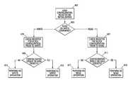
- FIG. 3illustrates a flowchart of one embodiment of a method for configuring the density/performance of a memory device.
- This embodimentuses special write and read commands to perform high density program and read operations.
- This embodimentputs the burden on the memory control circuitry to determine the density/performance configuration for a particular memory block. By having the control circuitry perform this task, the memory device does not require any extra hardware in order to switch blocks between high density and single density.
- the controllertracks the density/performance level.
- This embodimentuses two sets of algorithms—one for SBC reading and writing and another for MLC reading and writing.
- a higher level routinedetermines which set of algorithms to use depending on the received command.
- the erase operationis substantially similar for each memory density.
- the methoddetermines if the received command is a read or write command 301 . If a write command was received, it is determined 303 whether the command is a single density write command or a special high density write command.
- a high density write command 307causes the controller circuitry to program the specified memory block with two or more bits per cell.
- a single density write command 309causes the controller circuitry to program the specified memory block with one bit per cell.
- the received commandis a read command
- a single density configuration read commandcauses the memory block to be read 313 assuming it was programmed as an SBC.
- a configuration registeris used to pre-assign blocks of memory to the SBC or MLC configuration of operation. This could occur when the system is initialized. This embodiment would not require special commands than those used in MLC or SBC flash memory devices. Additionally, an existing register could be used to store the configuration data so that additional hardware is not required or, in another embodiment, a dedicated configuration register could be added to the memory device.
- the register of the present inventionhas a bit for every memory block for indicating the operating mode (e.g., MLC or SBC) of that particular block. For example, a logical 1 stored in the memory block 0 configuration bit would indicate that the block is an SBC block while a logical 0 would indicate the block is operating as an MLC block. In another embodiment, these logic levels are reversed.
- Alternate embodimentscan assign different quantities of blocks to each bit of the configuration register.
- the registermay have a configuration bit assigned to more than one memory block.
- a configuration bitmay be assigned to the sub-block level such that each block has multiple configuration bits.
- row 0 of the flash memory device of the present inventionis a configuration row.
- the configuration data from row 0is loaded into the configuration register 401 .
- a commandWhen a command is received, it is determined whether it is a read or write command 403 .
- the configuration registeris checked prior to the read operation to determine if the memory block has been assigned a high density or single density configuration 407 .
- a single density configuration 411a single density read operation is performed 419 .
- a high density read operationis performed 417 .
- the configuration registeris checked prior to write operation to determine if the memory block has been assigned a high density or a single density configuration 409 .
- a single density configuration 409a single density write operation is performed 415 .
- a high density write operationis performed 413 .
- the userdetermines the configuration of each block, or other memory cell grouping, and stores this data into the configuration register.
- the data in the configuration registeris copied to row 0 for more permanent storage in non-volatile memory.
- the usercan store the configuration directly to the non-volatile, configuration row of the memory device.
- the flash memory of the present inventionis comprised of memory blocks that can each be configured to store data in different densities. For example, one use of a single memory device might be to store both pictures and code. The picture data is more tolerant of corrupted data than the storage of code. Therefore, since the SBC configuration has a higher reliability than the MLC configuration, the user would typically choose the SBC configuration for the code storage and the MLC configuration for the picture storage.
- the MLC configurationmight be eight to nine times slower in read and programming performance as compared to the SBC configuration, the user might choose the MLC configuration for memory blocks requiring faster read/write times. This could be useful in a system having fast bus speeds requiring fast storage and retrieval times.
- the embodiments of the present inventionenable a memory device user to select between an MLC and an SBC configuration. Different configurations can be set up for different memory blocks or even to the sub-block level. Additionally, the configuration changes can be performed dynamically with configuration commands.
Landscapes
- Engineering & Computer Science (AREA)
- Computer Hardware Design (AREA)
- Read Only Memory (AREA)
- Dram (AREA)
- Logic Circuits (AREA)
Abstract
Description
Claims (24)
Priority Applications (6)
| Application Number | Priority Date | Filing Date | Title |
|---|---|---|---|
| US10/861,646US8082382B2 (en) | 2004-06-04 | 2004-06-04 | Memory device with user configurable density/performance |
| PCT/US2005/019898WO2005119695A2 (en) | 2004-06-04 | 2005-06-03 | Memory device with user configurable density/performance |
| KR1020077000135AKR100888113B1 (en) | 2004-06-04 | 2005-06-03 | Memory device with user configurable density/performance |
| JP2007515682AJP2008502090A (en) | 2004-06-04 | 2005-06-03 | Memory device with user-configurable density / operation performance |
| EP05760419AEP1754231A2 (en) | 2004-06-04 | 2005-06-03 | Memory device with user configurable density/performance |
| US13/305,809US20120072653A1 (en) | 2004-06-04 | 2011-11-29 | Memory device with user configurable density/performance |
Applications Claiming Priority (1)
| Application Number | Priority Date | Filing Date | Title |
|---|---|---|---|
| US10/861,646US8082382B2 (en) | 2004-06-04 | 2004-06-04 | Memory device with user configurable density/performance |
Related Child Applications (1)
| Application Number | Title | Priority Date | Filing Date |
|---|---|---|---|
| US13/305,809ContinuationUS20120072653A1 (en) | 2004-06-04 | 2011-11-29 | Memory device with user configurable density/performance |
Publications (2)
| Publication Number | Publication Date |
|---|---|
| US20050273549A1 US20050273549A1 (en) | 2005-12-08 |
| US8082382B2true US8082382B2 (en) | 2011-12-20 |
Family
ID=35310045
Family Applications (2)
| Application Number | Title | Priority Date | Filing Date |
|---|---|---|---|
| US10/861,646Expired - LifetimeUS8082382B2 (en) | 2004-06-04 | 2004-06-04 | Memory device with user configurable density/performance |
| US13/305,809AbandonedUS20120072653A1 (en) | 2004-06-04 | 2011-11-29 | Memory device with user configurable density/performance |
Family Applications After (1)
| Application Number | Title | Priority Date | Filing Date |
|---|---|---|---|
| US13/305,809AbandonedUS20120072653A1 (en) | 2004-06-04 | 2011-11-29 | Memory device with user configurable density/performance |
Country Status (5)
| Country | Link |
|---|---|
| US (2) | US8082382B2 (en) |
| EP (1) | EP1754231A2 (en) |
| JP (1) | JP2008502090A (en) |
| KR (1) | KR100888113B1 (en) |
| WO (1) | WO2005119695A2 (en) |
Cited By (2)
| Publication number | Priority date | Publication date | Assignee | Title |
|---|---|---|---|---|
| US20130132644A1 (en)* | 2011-11-23 | 2013-05-23 | Samsung Electronics Co., Ltd. | Method of programming a nonvolatile memory device |
| US8804452B2 (en) | 2012-07-31 | 2014-08-12 | Micron Technology, Inc. | Data interleaving module |
Families Citing this family (40)
| Publication number | Priority date | Publication date | Assignee | Title |
|---|---|---|---|---|
| US7469381B2 (en) | 2007-01-07 | 2008-12-23 | Apple Inc. | List scrolling and document translation, scaling, and rotation on a touch-screen display |
| US7535759B2 (en)* | 2004-06-04 | 2009-05-19 | Micron Technology, Inc. | Memory system with user configurable density/performance option |
| US7336531B2 (en) | 2004-06-25 | 2008-02-26 | Micron Technology, Inc. | Multiple level cell memory device with single bit per cell, re-mappable memory block |
| US7397700B2 (en) | 2005-04-11 | 2008-07-08 | Stmicroelectronics S.R.L. | Non-volatile memory electronic device with NAND structure being monolithically integrated on semiconductor |
| US7564721B2 (en)* | 2006-05-25 | 2009-07-21 | Micron Technology, Inc. | Method and apparatus for improving storage performance using a background erase |
| US7738291B2 (en)* | 2007-03-12 | 2010-06-15 | Micron Technology, Inc. | Memory page boosting method, device and system |
| US7460398B1 (en)* | 2007-06-19 | 2008-12-02 | Micron Technology, Inc. | Programming a memory with varying bits per cell |
| KR101303177B1 (en)* | 2007-06-22 | 2013-09-17 | 삼성전자주식회사 | Non-volatile memory device and operating method of the same |
| KR20090021508A (en)* | 2007-08-27 | 2009-03-04 | 삼성전자주식회사 | Flash memory device and program method thereof for storing data in multi-bit and single-bit manner |
| US7817467B2 (en) | 2007-09-07 | 2010-10-19 | Micron Technology, Inc. | Memory controller self-calibration for removing systemic influence |
| WO2009064619A1 (en)* | 2007-11-16 | 2009-05-22 | Rambus Inc. | Apparatus and method for segmentation of a memory device |
| KR20090055314A (en) | 2007-11-28 | 2009-06-02 | 삼성전자주식회사 | Nonvolatile Memory Devices Can Reduce Read Disruptions |
| US8341331B2 (en)* | 2008-04-10 | 2012-12-25 | Sandisk Il Ltd. | Method, apparatus and computer readable medium for storing data on a flash device using multiple writing modes |
| US20100057976A1 (en)* | 2008-08-26 | 2010-03-04 | Menahem Lasser | Multiple performance mode memory system |
| US7984200B1 (en)* | 2008-09-23 | 2011-07-19 | Western Digital Technologies, Inc. | Configuring a data storage device with a configuration data record set in response to a configuration code |
| US9009358B1 (en) | 2008-09-23 | 2015-04-14 | Western Digital Technologies, Inc. | Configuring a data storage device with a parameter file interlocked with configuration code |
| US7852671B2 (en) | 2008-10-30 | 2010-12-14 | Micron Technology, Inc. | Data path for multi-level cell memory, methods for storing and methods for utilizing a memory array |
| US8407400B2 (en)* | 2008-11-12 | 2013-03-26 | Micron Technology, Inc. | Dynamic SLC/MLC blocks allocations for non-volatile memory |
| KR101519931B1 (en) | 2009-03-06 | 2015-05-13 | 삼성전자주식회사 | Resistive memory device having a stack structure memory system having the resistive memory device and method of setting cell type of stacked memory cell array layers |
| US8489841B1 (en) | 2009-12-10 | 2013-07-16 | Western Digital Technologies, Inc. | Manufacturing station dynamically configuring a data storage device with a validated configuration data record |
| US8671240B2 (en) | 2011-07-18 | 2014-03-11 | Memory Technologies Llc | User selectable balance between density and reliability |
| JP5744118B2 (en) | 2013-07-17 | 2015-07-01 | ウィンボンド エレクトロニクス コーポレーション | Semiconductor memory device |
| US10503388B2 (en) | 2013-09-03 | 2019-12-10 | Apple Inc. | Crown input for a wearable electronic device |
| US12287962B2 (en) | 2013-09-03 | 2025-04-29 | Apple Inc. | User interface for manipulating user interface objects |
| KR102111452B1 (en)* | 2013-09-03 | 2020-05-15 | 애플 인크. | User interface for manipulating user interface objects |
| CN110795005A (en) | 2013-09-03 | 2020-02-14 | 苹果公司 | User interface for manipulating user interface objects using magnetic properties |
| US11068128B2 (en) | 2013-09-03 | 2021-07-20 | Apple Inc. | User interface object manipulations in a user interface |
| EP3147747A1 (en) | 2014-06-27 | 2017-03-29 | Apple Inc. | Manipulation of calendar application in device with touch screen |
| TWI676127B (en) | 2014-09-02 | 2019-11-01 | 美商蘋果公司 | Method, system, electronic device and computer-readable storage medium regarding electronic mail user interface |
| CN106797493A (en) | 2014-09-02 | 2017-05-31 | 苹果公司 | Music user interface |
| TWI582641B (en) | 2014-09-02 | 2017-05-11 | 蘋果公司 | Button functionality |
| US20160062571A1 (en) | 2014-09-02 | 2016-03-03 | Apple Inc. | Reduced size user interface |
| US10096355B2 (en) | 2015-09-01 | 2018-10-09 | Sandisk Technologies Llc | Dynamic management of programming states to improve endurance |
| US9620201B1 (en)* | 2016-04-26 | 2017-04-11 | Sandisk Technologies Llc | Storage system and method for using hybrid blocks with sub-block erase operations |
| US10152237B2 (en) | 2016-05-05 | 2018-12-11 | Micron Technology, Inc. | Non-deterministic memory protocol |
| US10534540B2 (en) | 2016-06-06 | 2020-01-14 | Micron Technology, Inc. | Memory protocol |
| US9940052B2 (en) | 2016-09-14 | 2018-04-10 | Micron Technology, Inc. | Memory device configuration commands |
| US20180292991A1 (en)* | 2017-04-11 | 2018-10-11 | Micron Technology, Inc. | Memory protocol with programmable buffer and cache size |
| US11435830B2 (en) | 2018-09-11 | 2022-09-06 | Apple Inc. | Content-based tactile outputs |
| US11537511B2 (en) | 2020-08-05 | 2022-12-27 | Infineon Technologies LLC | Dynamic configuring of reliability and density of non-volatile memories |
Citations (15)
| Publication number | Priority date | Publication date | Assignee | Title |
|---|---|---|---|---|
| US20010038553A1 (en)* | 2000-02-25 | 2001-11-08 | Advanced Micro Devices, Inc. | Mixed mode multi-level memory |
| US6349395B2 (en) | 1997-09-17 | 2002-02-19 | Kabushiki Kaisha Toshiba | Configurable integrated circuit and method of testing the same |
| US6353553B1 (en)* | 2000-01-24 | 2002-03-05 | Mitsubishi Denki Kabushiki Kaisha | Nonvolatile semiconductor memory device having structure storing multivalued data and data storage system comprising the nonvolatile semiconductor memory device |
| US6363008B1 (en) | 2000-02-17 | 2002-03-26 | Multi Level Memory Technology | Multi-bit-cell non-volatile memory with maximized data capacity |
| US20020054504A1 (en)* | 2000-09-20 | 2002-05-09 | Stmicroelectronics S.R.I. | Nonvolatile memory device, having parts with different access time, reliablity, and capacity |
| US20020057595A1 (en)* | 2000-01-19 | 2002-05-16 | Shinichi Kobayashi | Variable capacity semiconductor memory device |
| US20020144103A1 (en)* | 2001-03-29 | 2002-10-03 | Kendall Terry L. | Non-volatile alterable default flash memory configuration registers |
| US6466476B1 (en) | 2001-01-18 | 2002-10-15 | Multi Level Memory Technology | Data coding for multi-bit-per-cell memories having variable numbers of bits per memory cell |
| US20030041210A1 (en)* | 2001-08-24 | 2003-02-27 | Micron Technology, Inc. | Erase block management |
| US6542909B1 (en)* | 1998-06-30 | 2003-04-01 | Emc Corporation | System for determining mapping of logical objects in a computer system |
| US20030131185A1 (en)* | 2002-01-04 | 2003-07-10 | Lance Dover | Flash memory command abstraction |
| US20030165076A1 (en)* | 2001-09-28 | 2003-09-04 | Gorobets Sergey Anatolievich | Method of writing data to non-volatile memory |
| US6640262B1 (en) | 1999-12-20 | 2003-10-28 | 3Com Corporation | Method and apparatus for automatically configuring a configurable integrated circuit |
| US6662285B1 (en) | 2001-01-09 | 2003-12-09 | Xilinx, Inc. | User configurable memory system having local and global memory blocks |
| US7535759B2 (en) | 2004-06-04 | 2009-05-19 | Micron Technology, Inc. | Memory system with user configurable density/performance option |
Family Cites Families (1)
| Publication number | Priority date | Publication date | Assignee | Title |
|---|---|---|---|---|
| US6209069B1 (en)* | 1998-05-11 | 2001-03-27 | Intel Corporation | Method and apparatus using volatile lock architecture for individual block locking on flash memory |
- 2004
- 2004-06-04USUS10/861,646patent/US8082382B2/ennot_activeExpired - Lifetime
- 2005
- 2005-06-03JPJP2007515682Apatent/JP2008502090A/ennot_activeWithdrawn
- 2005-06-03EPEP05760419Apatent/EP1754231A2/ennot_activeWithdrawn
- 2005-06-03KRKR1020077000135Apatent/KR100888113B1/ennot_activeExpired - Lifetime
- 2005-06-03WOPCT/US2005/019898patent/WO2005119695A2/enactiveApplication Filing
- 2011
- 2011-11-29USUS13/305,809patent/US20120072653A1/ennot_activeAbandoned
Patent Citations (16)
| Publication number | Priority date | Publication date | Assignee | Title |
|---|---|---|---|---|
| US6349395B2 (en) | 1997-09-17 | 2002-02-19 | Kabushiki Kaisha Toshiba | Configurable integrated circuit and method of testing the same |
| US6542909B1 (en)* | 1998-06-30 | 2003-04-01 | Emc Corporation | System for determining mapping of logical objects in a computer system |
| US6640262B1 (en) | 1999-12-20 | 2003-10-28 | 3Com Corporation | Method and apparatus for automatically configuring a configurable integrated circuit |
| US20020057595A1 (en)* | 2000-01-19 | 2002-05-16 | Shinichi Kobayashi | Variable capacity semiconductor memory device |
| US6353553B1 (en)* | 2000-01-24 | 2002-03-05 | Mitsubishi Denki Kabushiki Kaisha | Nonvolatile semiconductor memory device having structure storing multivalued data and data storage system comprising the nonvolatile semiconductor memory device |
| US6363008B1 (en) | 2000-02-17 | 2002-03-26 | Multi Level Memory Technology | Multi-bit-cell non-volatile memory with maximized data capacity |
| US20010038553A1 (en)* | 2000-02-25 | 2001-11-08 | Advanced Micro Devices, Inc. | Mixed mode multi-level memory |
| US20020054504A1 (en)* | 2000-09-20 | 2002-05-09 | Stmicroelectronics S.R.I. | Nonvolatile memory device, having parts with different access time, reliablity, and capacity |
| US6662285B1 (en) | 2001-01-09 | 2003-12-09 | Xilinx, Inc. | User configurable memory system having local and global memory blocks |
| US6466476B1 (en) | 2001-01-18 | 2002-10-15 | Multi Level Memory Technology | Data coding for multi-bit-per-cell memories having variable numbers of bits per memory cell |
| US20020144103A1 (en)* | 2001-03-29 | 2002-10-03 | Kendall Terry L. | Non-volatile alterable default flash memory configuration registers |
| US20030041210A1 (en)* | 2001-08-24 | 2003-02-27 | Micron Technology, Inc. | Erase block management |
| US20030165076A1 (en)* | 2001-09-28 | 2003-09-04 | Gorobets Sergey Anatolievich | Method of writing data to non-volatile memory |
| US20030131185A1 (en)* | 2002-01-04 | 2003-07-10 | Lance Dover | Flash memory command abstraction |
| US7535759B2 (en) | 2004-06-04 | 2009-05-19 | Micron Technology, Inc. | Memory system with user configurable density/performance option |
| US20090213655A1 (en) | 2004-06-04 | 2009-08-27 | Micron Technology, Inc. | Memory system with user configurable density/performance option |
Cited By (3)
| Publication number | Priority date | Publication date | Assignee | Title |
|---|---|---|---|---|
| US20130132644A1 (en)* | 2011-11-23 | 2013-05-23 | Samsung Electronics Co., Ltd. | Method of programming a nonvolatile memory device |
| US8804452B2 (en) | 2012-07-31 | 2014-08-12 | Micron Technology, Inc. | Data interleaving module |
| US9189440B2 (en) | 2012-07-31 | 2015-11-17 | Micron Technology, Inc. | Data interleaving module |
Also Published As
| Publication number | Publication date |
|---|---|
| KR20070024702A (en) | 2007-03-02 |
| WO2005119695A2 (en) | 2005-12-15 |
| EP1754231A2 (en) | 2007-02-21 |
| WO2005119695A3 (en) | 2006-02-02 |
| US20050273549A1 (en) | 2005-12-08 |
| KR100888113B1 (en) | 2009-03-13 |
| US20120072653A1 (en) | 2012-03-22 |
| JP2008502090A (en) | 2008-01-24 |
Similar Documents
| Publication | Publication Date | Title |
|---|---|---|
| US8082382B2 (en) | Memory device with user configurable density/performance | |
| US8644065B2 (en) | Memory system with user configurable density/performance option | |
| US7336531B2 (en) | Multiple level cell memory device with single bit per cell, re-mappable memory block | |
| KR100878479B1 (en) | Memory system that determines program method based on data information | |
| US11133071B2 (en) | Charge loss failure mitigation | |
| US20060193176A1 (en) | Multiple level programming in a non-volatile memory device | |
| KR20080067834A (en) | Programmable memory system | |
| US10636482B2 (en) | Methods of operating a memory with redistribution of received data | |
| US7317635B2 (en) | User configurable commands for flash memory | |
| CN111797030A (en) | Memory containing search logic and method for performing a search within said memory |
Legal Events
| Date | Code | Title | Description |
|---|---|---|---|
| AS | Assignment | Owner name:MICRON TECHNOLOGY, INC., IDAHO Free format text:ASSIGNMENT OF ASSIGNORS INTEREST;ASSIGNOR:ROOHPARVAR, FRANKIE F.;REEL/FRAME:015441/0993 Effective date:20040520 | |
| FEPP | Fee payment procedure | Free format text:PAYOR NUMBER ASSIGNED (ORIGINAL EVENT CODE: ASPN); ENTITY STATUS OF PATENT OWNER: LARGE ENTITY | |
| STCF | Information on status: patent grant | Free format text:PATENTED CASE | |
| CC | Certificate of correction | ||
| FPAY | Fee payment | Year of fee payment:4 | |
| AS | Assignment | Owner name:U.S. BANK NATIONAL ASSOCIATION, AS COLLATERAL AGENT, CALIFORNIA Free format text:SECURITY INTEREST;ASSIGNOR:MICRON TECHNOLOGY, INC.;REEL/FRAME:038669/0001 Effective date:20160426 Owner name:U.S. BANK NATIONAL ASSOCIATION, AS COLLATERAL AGEN Free format text:SECURITY INTEREST;ASSIGNOR:MICRON TECHNOLOGY, INC.;REEL/FRAME:038669/0001 Effective date:20160426 | |
| AS | Assignment | Owner name:MORGAN STANLEY SENIOR FUNDING, INC., AS COLLATERAL AGENT, MARYLAND Free format text:PATENT SECURITY AGREEMENT;ASSIGNOR:MICRON TECHNOLOGY, INC.;REEL/FRAME:038954/0001 Effective date:20160426 Owner name:MORGAN STANLEY SENIOR FUNDING, INC., AS COLLATERAL Free format text:PATENT SECURITY AGREEMENT;ASSIGNOR:MICRON TECHNOLOGY, INC.;REEL/FRAME:038954/0001 Effective date:20160426 | |
| AS | Assignment | Owner name:U.S. BANK NATIONAL ASSOCIATION, AS COLLATERAL AGENT, CALIFORNIA Free format text:CORRECTIVE ASSIGNMENT TO CORRECT THE REPLACE ERRONEOUSLY FILED PATENT #7358718 WITH THE CORRECT PATENT #7358178 PREVIOUSLY RECORDED ON REEL 038669 FRAME 0001. ASSIGNOR(S) HEREBY CONFIRMS THE SECURITY INTEREST;ASSIGNOR:MICRON TECHNOLOGY, INC.;REEL/FRAME:043079/0001 Effective date:20160426 Owner name:U.S. BANK NATIONAL ASSOCIATION, AS COLLATERAL AGEN Free format text:CORRECTIVE ASSIGNMENT TO CORRECT THE REPLACE ERRONEOUSLY FILED PATENT #7358718 WITH THE CORRECT PATENT #7358178 PREVIOUSLY RECORDED ON REEL 038669 FRAME 0001. ASSIGNOR(S) HEREBY CONFIRMS THE SECURITY INTEREST;ASSIGNOR:MICRON TECHNOLOGY, INC.;REEL/FRAME:043079/0001 Effective date:20160426 | |
| AS | Assignment | Owner name:JPMORGAN CHASE BANK, N.A., AS COLLATERAL AGENT, ILLINOIS Free format text:SECURITY INTEREST;ASSIGNORS:MICRON TECHNOLOGY, INC.;MICRON SEMICONDUCTOR PRODUCTS, INC.;REEL/FRAME:047540/0001 Effective date:20180703 Owner name:JPMORGAN CHASE BANK, N.A., AS COLLATERAL AGENT, IL Free format text:SECURITY INTEREST;ASSIGNORS:MICRON TECHNOLOGY, INC.;MICRON SEMICONDUCTOR PRODUCTS, INC.;REEL/FRAME:047540/0001 Effective date:20180703 | |
| AS | Assignment | Owner name:MICRON TECHNOLOGY, INC., IDAHO Free format text:RELEASE BY SECURED PARTY;ASSIGNOR:U.S. BANK NATIONAL ASSOCIATION, AS COLLATERAL AGENT;REEL/FRAME:047243/0001 Effective date:20180629 | |
| MAFP | Maintenance fee payment | Free format text:PAYMENT OF MAINTENANCE FEE, 8TH YEAR, LARGE ENTITY (ORIGINAL EVENT CODE: M1552); ENTITY STATUS OF PATENT OWNER: LARGE ENTITY Year of fee payment:8 | |
| AS | Assignment | Owner name:MICRON TECHNOLOGY, INC., IDAHO Free format text:RELEASE BY SECURED PARTY;ASSIGNOR:MORGAN STANLEY SENIOR FUNDING, INC., AS COLLATERAL AGENT;REEL/FRAME:050937/0001 Effective date:20190731 | |
| AS | Assignment | Owner name:MICRON SEMICONDUCTOR PRODUCTS, INC., IDAHO Free format text:RELEASE BY SECURED PARTY;ASSIGNOR:JPMORGAN CHASE BANK, N.A., AS COLLATERAL AGENT;REEL/FRAME:051028/0001 Effective date:20190731 Owner name:MICRON TECHNOLOGY, INC., IDAHO Free format text:RELEASE BY SECURED PARTY;ASSIGNOR:JPMORGAN CHASE BANK, N.A., AS COLLATERAL AGENT;REEL/FRAME:051028/0001 Effective date:20190731 | |
| MAFP | Maintenance fee payment | Free format text:PAYMENT OF MAINTENANCE FEE, 12TH YEAR, LARGE ENTITY (ORIGINAL EVENT CODE: M1553); ENTITY STATUS OF PATENT OWNER: LARGE ENTITY Year of fee payment:12 |