US8078918B2 - Solid state storage subsystem that maintains and provides access to data reflective of a failure risk - Google Patents
Solid state storage subsystem that maintains and provides access to data reflective of a failure riskDownload PDFInfo
- Publication number
- US8078918B2 US8078918B2US12/027,965US2796508AUS8078918B2US 8078918 B2US8078918 B2US 8078918B2US 2796508 AUS2796508 AUS 2796508AUS 8078918 B2US8078918 B2US 8078918B2
- Authority
- US
- United States
- Prior art keywords
- data
- storage subsystem
- host system
- sensor
- errors
- Prior art date
- Legal status (The legal status is an assumption and is not a legal conclusion. Google has not performed a legal analysis and makes no representation as to the accuracy of the status listed.)
- Active, expires
Links
Images


Classifications
- G—PHYSICS
- G06—COMPUTING OR CALCULATING; COUNTING
- G06F—ELECTRIC DIGITAL DATA PROCESSING
- G06F11/00—Error detection; Error correction; Monitoring
- G06F11/008—Reliability or availability analysis
Definitions
- the present disclosurerelates to storage subsystems that use solid-state memory devices. More specifically, the present disclosure relates to systems and methods for assessing a risk of a storage subsystem failure.
- Solid-state storage subsystemsare used to store a wide variety of data. With increasing memory capacity, a mixture of information (e.g., program files, set-up files, user data, etc.) corresponding to a variety of storage applications can be conveniently stored on a single solid-state storage subsystem, such as a removable flash memory card or drive that attaches to a host computer. Many of these storage applications demand high levels of data integrity over the life of the subsystem.
- SiliconSystems, Inc.the assignee of the present application, sells solid-state storage subsystems that maintain usage statistics regarding the number of program/erase cycles that have been performed in the non-volatile memory array. These usage statistics can be read out using vendor-specific commands, and can be used to estimate the remaining life of the memory array.
- This technologyis commercially known as SiSmartTM, and aspects of this technology are disclosed in co-pending U.S. application Ser. No. 11/429,936, filed May 8, 2006, the disclosure of which is hereby incorporated by reference.
- usage statistics regarding numbers of program/erase cycles performedare very useful for predicting wear-related failures, they are less useful for predicting failures caused by other conditions. Further, in some situations, such usage statistics are not sufficient to reliably predict the timing of wear-related failures. This may be the case where, for example, a particular memory device has a lower endurance than others, meaning that it will fail after a lesser number of program/erase cycles. Such variations in endurance can be caused by manufacturing irregularities or unusual operating conditions.
- the present disclosureaddresses these issues by providing a storage subsystem that maintains at least one of the following types of data: (a) statistics regarding errors detected via an ECC (error correction code) module of the storage subsystem; (b) historical data regarding operating conditions experienced by the storage subsystem, such as temperature, altitude, humidity, shock, and/or input voltage level.
- the storage subsystem, and/or a host system to which the storage subsystem attachesmay analyze the stored data to assess a risk of a failure event, such as an uncorrectable data error.
- the results of this analysismay be displayed via a user interface of the host system, and/or may be used to automatically take a precautionary action such as transmitting an alert message or changing a mode of operation of the storage subsystem.
- the storage subsystemmay also maintain usage statistics regarding numbers of program/erase cycles performed.
- FIG. 1illustrates a block diagram of a storage subsystem connected to a host system according to one embodiment
- FIG. 2illustrates a display screen for displaying monitor data and estimated risk levels according to one embodiment
- FIG. 3illustrates a flow chart showing a process for monitoring operating and environmental conditions of a storage subsystem, determining a risk level, and displaying the data according to one embodiment
- FIG. 4illustrates a block diagram showing a plurality of storage subsystems connected to a host system.
- FIG. 1is a block diagram illustrating a host system 110 connected to a storage subsystem 112 according to one embodiment.
- the host system 110may, for example, be a portable computer, a workstation, a router, a handheld instrument system, a computing kiosk, a blade server, a military system, a flight computer, or any other type of computing device.
- the host system 110stores data on the storage subsystem 112 , and may provide operating system functionality and a boot process for the storage subsystem 112 .
- the host system 110executes a driver program 113 that provides functionality for communicating with the storage subsystem 112 , such as by issuing commands in accordance with an ATA (Advanced Technology Attachment) signal interface or other standard.
- the driver 113may communicate with, or be part of, one or more software applications that are configured to use the storage subsystem 112 .
- ATAAdvanced Technology Attachment
- the storage subsystem 112may be in the form of a portable, detachable device, such as a solid-state memory card or drive, that plugs into a slot or external port of the host system 110 .
- the storage subsystemmay comply with one or more of the following specifications: CompactFlash, PCMCIA, SmartMedia, MultiMediaCard, SecureDigital, Memory Stick, ATA, ATAPI, PCI Express, PCI Mezzanine Card, AdvancedTCA Mezzanine Card, SATA (Serial Advanced Technology Attachment), or Universal Serial Bus (USB).
- the storage subsystempluggably connects to the host system, and receives power from the host system, via a physical/electrical connector 111 , such as a USB, CompactFlash, PCMCIA, SATA, or proprietary (non-standard) connector.
- the storage subsystem 112comprises a controller 114 and a solid-state non-volatile memory (NVM) array 116 .
- the NVM array 116is preferably implemented using flash memory devices, but may be implemented using another type of solid state device, such as volatile memory devices (e.g., DRAM or SRAM) backed up by battery.
- the storage subsystem 112may also include another type of non-volatile storage, such as one or more miniature magnetic disk drives (not shown).
- the controller 114is configured to write data to, and read data from, the NVM array 116 in response to commands from the host 110 .
- the controller 114includes an error correction code (ECC) module 115 that (1) generates sector-level ECC data when the host 110 writes data to the storage subsystem, and (2) performs ECC checking (including correction of correctable errors) when the host reads data from the storage subsystem.
- ECCerror correction code
- the controller 114is typically implemented as a single integrated circuit device, but may alternatively comprise multiple distinct devices.
- the controller 114is an ATA flash disk controller that executes a firmware program which embodies the various features described herein. Some or all of the functions of the controller 114 (including ECC generation and checking) may alternatively be automated in application-specific circuitry.
- the non-volatile memory array 116is preferably divided into blocks, and each block is divided into sectors.
- the sectors and blocksare configured and used generally as follows: (1) each sector preferably stores 512 bytes of data plus some number of bytes (e.g., 16) of management data; (2) a sector represents the smallest unit of data that can be written to or read from the NVM array; (3) the management data stored in each sector includes ECC (error correction code) data that is generated by the controller 114 on write operations, and used by the controller 114 on read operations to check for and correct errors; (4) a block is the smallest unit of data that can be erased with an erase command; the blocks may, for example, have a size of 128 k+4 k bytes.
- the errors corrected using the ECC datamay be the result of wear, environmental conditions, and other types of conditions.
- the controller 114implements a wear-leveling algorithm to reduce the likelihood that certain sectors or blocks will fail long before others.
- the NVM array 116is preferably subdivided into a user data area 118 and a restricted area 120 .
- the address ranges of these two areasneed not be contiguous; for example, portions of the restricted space may be interleaved with portions of the user data space.
- the user data area 118is read/write accessible via standard (e.g., ATA) access commands, and is used by the controller 114 to implement a conventional file system (e.g., FAT16 or FAT32).
- a conventional file systeme.g., FAT16 or FAT32
- the restricted memory area 120is preferably accessible only via one or more non-standard or “vendor-specific” commands, and thus is not exposed to the host's operating system and applications. Stated differently, the standard memory access command codes used to access the subsystem's user data area 118 do not provide access to the restricted area 120 . As described below, the restricted area 120 is used to store configuration and control information, including monitor data 121 . In other embodiments of the invention, the restricted area 120 may be omitted; in such embodiments, the data described herein as being stored in the restricted area 120 may be stored in the user data area 118 , or on a separate storage device (e.g. a magnetic disk drive).
- a separate storage devicee.g. a magnetic disk drive
- the restricted area 120may also be used by the controller 114 to store other types of control information.
- the restricted area 120may store firmware executed by the controller 114 , security information for controlling access to the user data area 118 , and/or wear level data reflective of the wear level of each sector or block of the NVM array 116 .
- the storage system 112 in the illustrated embodimentfurther includes one or more sensors 125 that sense, and transmit data/signals indicative of, environmental conditions such as temperature, humidity, altitude, and/or storage subsystem movement.
- the sensor data detected by the sensor(s) 125may be read by the controller 114 and stored in the restricted area 120 of the NVM array 116 .
- the controllermay periodically read a measurement value from a sensor 125 , and maintain a record of the highest and lowest measurement values read since the storage subsystem's initial use.
- Multiple sensors of different typesmay be provided, such as a temperature sensor, a humidity sensor, an accelerometer, an altimeter, or any combination thereof.
- the storage subsystemdoes not include a sensor 125 .
- the sensor datais one type of monitor data 121 that may be stored by the storage subsystem 112 and used to determine a risk of data errors occurring.
- Other types of monitor datainclude parameters that may be sensed or generated by the controller 114 or by another circuit of the storage subsystem.
- the controller 114may generate and store monitor data 121 that describes the stability of the power signal from the host (e.g., number of anomalies detected per unit time, average anomaly duration, etc.), as detected by a power-anomaly detection circuit.
- the controller 114may generate and store monitor data 121 descriptive correctable (and possibly uncorrectable) data errors detected on read operations. Examples of specific data-error-rate metrics that may be maintained by the storage subsystem are described below. Other examples of types of monitor data 121 that may be collected include (1) the duration since the last subsystem power-up event, (2) an average subsystem ON time, (3) the total (cumulative) ON time, (4) the number write operations that have failed to complete due to a loss of power and (5) usage statistics regarding numbers of program/erase cycles performed (as described in the above-referenced application). As illustrated in FIG. 1 , some or all types of monitor data 121 may be stored in the restricted area 120 . Some types of monitor data, such as “duration since the last subsystem power-up event,” may alternatively be maintained in volatile storage, or may be read directly from a sensor when needed.
- the host system 110can access the monitor data 121 via one or more vendor-specific (non-standard) commands, or via a special signal interface between the host 110 and the storage subsystem 112 .
- the storage subsystemmay compile this data (or a summarized version thereof) into a fixed-size block that is readable by the host system, and which is arranged according to a format known to the host system's driver 113 .
- the host system's driver 113or an application that communicates with the driver, may make this data available for viewing on the host system 110 via a special user interface.
- the host 110 and/or the controller 114may also analyze the stored monitor data 121 to assess a risk level associated with the occurrence of data errors.
- the monitor data 121may indicate that the storage subsystem 112 is operating in an extreme temperature range (e.g., over 60° C.), or that the bit error rate has exceeded a particular threshold.
- an alert messagemay be generated and displayed on the host system 110 , as described below.
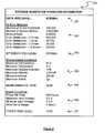
- Table 1illustrates examples of particular variables that may be used by the controller 114 to maintain bit error statistics. Each variable may correspond to a particular sequence of bytes in the restricted memory area, and may be updated by the controller 114 as corresponding events occur. As will be recognized, these variables are merely illustrative, and other variables may be used to accomplish similar functions.
- the first two variables shown in Table 1are used to keep track of (1) the total number of times a sector read resulted in a correctable error, and (2) the total number of sector write operations that have been performed. These two variables are global in the sense that they store subsystem-level statistics, rather than sector-level or block-level statistics. These first two variables may be used in combination to compute a ratio of corrected errors to total number of sectors writes.
- the variable “Number of Sector Writes”may be incremented by 1 every time a sector write is performed, or may be incremented by N (e.g., 16 or 32) on every Nth sector write.
- the next seven variables(“Number of Reads with ⁇ > Errors”) can be used to maintain additional statistics regarding the detected errors.
- Each of these variablesmaintains a storage-subsystem-wide count value.
- the count value/variableis incremented that corresponds to the number of bits that needed to be corrected. For example, if no bits needed to be corrected, “Number of Reads with 0 Errors” would be incremented; and if two bits needed to be corrected, “Number of Reads with 2 Errors” would be incremented.
- the last variableis the bit error rate (BER), and may be calculated as: (Number of bits with errors)/(Number of sector reads ⁇ 4224 bits/sector). This value indicates the rate of error occurrences in the storage subsystem. Rather than maintaining the BER in non-volatile storage, the controller 114 may generate it on-the-fly when requested by the host 110 or when otherwise needed. Further, the BER could alternatively be generated by the host 110 from the stored variables.
- BERbit error rate
- Additional variablesmay optionally be provided to track errors and usage at the block and/or sector level.
- one or more variablesmay be provided for maintaining “short term” bit error statistics, such as “BER since last power up” or “BER over last minute.”
- the monitor data 121may include event timestamps that indicate when (date and time) the associated measurements were taken or when particular anomalies were detected.
- event metadatamay also be stored, such as one or more of the following: (1) an identifier of the host 110 connected to the storage subsystem 112 at the time a particular anomaly was detected, (2) an identifier of the type of operation being performed when a particular anomaly was detected, (3) an indication of how long the storage subsystem had been ON when a particular anomaly was detected, (4) the amount of time since the host 110 last performed a read of the monitor data 121 .
- the timestamps and other types of event metadatamay be used by the host system 110 and/or the controller 114 for various purposes, such as to correlate detected error conditions (e.g., a rapid increase in the bit error rate) with particular environmental conditions (e.g., a relatively high operating temperature or humidity level). Where such correlations are detected, the host system 110 and/or the controller 114 may automatically take an appropriate corrective action. For example, if the host 110 or the controller 114 detects that a relatively high bit error rate occurs when the operating temperature exceeds a particular threshold, it may do one or both of the following: (1) adjust the temperature threshold used to generate alert messages, (2) cause the controller 114 to slow its operation (to reduce heat generation) whenever this temperature threshold is reached or exceeded. In embodiments in which the controller 114 is capable of detecting such correlations, the controller 114 may store descriptions of the detected correlations in the NVM array, and may provide host access to these descriptions.
- detected error conditionse.g., a rapid increase in the bit error rate
- environmental conditionse.g
- the storage subsystem 112may also be configured to store monitor data 121 generated by one or more sensors of the host system 110 .
- the host system 110may include one or more sensors 123 that measure(s) temperature, humidity, altitude, or storage subsystem movement.
- the host system's driver 113may write the host-generated sensor data to the storage subsystem's restricted area 120 using vendor-specific commands.
- the host-generated sensor datamay supplement subsystem-generated sensor data, and may be used for the same purposes.
- the storage subsystemmay include a small display unit, such as a LCD screen or one or more LEDs.
- This display unitmay be used to output a summary indication of the risk level, such as by displaying a single word, color, or icon that represents the risk level.
- the ability for the host to access the monitor datamay optionally be omitted.
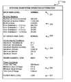
- FIG. 2illustrates a display screen 200 generated based on monitor data 121 read from the storage subsystem 112 according to one embodiment.
- the display screen 200is generated by the driver 113 , or application-level software, running on the host system 110 .
- the display screenmay, for example, be accessible by clicking on a task bar icon, and may be updated periodically as new monitor data is read from the storage subsystem 112 .
- the host software that generates the display screen 200may also generate alert messages that are displayed on the host system 110 and/or communicated by e-mail.
- the display screen 200shows bit error statistics 202 , environmental conditions 204 , and power conditions 206 , as monitored by the storage subsystem 112 (and in some cases, the host system 110 ).
- the bit error statisticsinclude the following: number of errors corrected, number of sector writes performed, bit error rate, and the numbers of reads with zero errors, 1 error, 2 errors, and 2+ errors. These statistics correspond to specific variables shown in Table 1.
- the number of sector writesmay indicate a general wear level of the NVM array 116 and may also be used in conjunction with the number of errors corrected to determine a bit error rate. In the example shown, the bit error rate is approximately 0.00005, which is one bit error for every 20,000 bits written.
- the BERmay be calculated by the controller 114 (e.g., in response to a vendor-specific command received from the host system) or by the host 110 .
- the display screen 200includes a summarized bit error risk level 203 .
- the bit error risk level 203corresponds to an assessment of the likelihood of an uncorrectable data error occurring in the storage subsystem 112 , as determined from the bit error statistics. Based on the example in FIG. 2 , a BER less than 0.000001 would be “low,” and a BER between 0.000001 and 0.0001 would be “normal.” A BER between 0.0001 and 0.001 would be “high” and a BER over 0.001 would be “very high.” Those skilled in the art will recognize that these numbers are for illustrative purposes only and embodiments may have different risk level definitions in accordance to the needs of the systems.
- the bit error risk levelis “normal.”
- the bit error risk level 203and the other displayed risk levels 201 , 205 and 207 (each discussed below), may be determined by the controller 114 (e.g., via firmware or application specific circuitry) or by the host system 110 .
- only the risk levels 201 , 203 , 205 and 207are displayed, and not the associated numerical data from which these risk levels are derived.
- the risk levels 201 , 203 , 205 and 207may, for example, have possible states of “low,” “normal,” “high” and “very high,” or may be displayed as numerical values, such as percentages.
- the environmental conditions 204 shown in FIG. 2include a maximum temperature, a minimum temperature, a maximum relative humidity, a maximum altitude, a minimum altitude, and a maximum shock level.
- the controller 114may maintain these values in the restricted memory area 120 as respective 2-byte data values. The values are preferably based on sensor measurements read by the controller since the inception (initial use or initialization) of the storage subsystem. Additional or alternative environmental parameters, such as a current temperature, may be monitored and displayed. As mentioned above, the environmental conditions are monitored by the storage subsystem 112 , and in some cases, the host 110 , using one or more sensors 125 , 123 .
- the maximum and minimum temperature fieldsdisplay the maximum and minimum temperatures detected by the storage subsystem 112 (or the host system 110 ) during storage subsystem operation. In the example shown, the highest detected temperature is 87° C., and the lowest is 5° C. A very high or very low temperature may correlate with an increase in the likelihood of an uncorrectable data error.
- the maximum relative humidity fielddisplays the maximum humidity detected by the storage subsystem 112 (or the host system 110 ) during storage subsystem operation. A high relative humidity may correlate with an increased probability of data errors. In the example shown, the maximum relative humidity is 15%.
- the maximum and minimum altitude fieldsdisplay the maximum and minimum altitude as detected by an altimeter 125 of the storage subsystem 112 and/or an altimeter sensor 123 of the host system 110 .
- Extreme altitudesmay correspond to conditions, such as temperature or air pressure, that may be related to the risk of data errors in the storage subsystem 112 .
- the maximum shock fieldmay measure whether the storage subsystem has been exposed to extreme shock, which may result in system or device failure, or may correspond to an increased likelihood of data errors. In the example shown, the maximum shock is 2 g.
- the environmental risk indicator 205indicates a risk of an uncorrectable storage subsystem data error, as determined from the monitored environmental conditions. This indicator may, in some embodiments, reflect observed correlations between error occurrences and environmental conditions. For example, if the controller 114 or host 110 has previously detected significant increases in the bit error rate when the temperature is above a threshold level, it may set the environmental risk level 205 to “high” whenever this temperature is reached or exceeded. The environmental risk indicator 205 may alternatively be based on fixed (predefined) thresholds.
- the power conditions 206include a power ON time, a maximum input voltage, a minimum input voltage, and a time out-of-range field.
- the power conditionsare monitored by the storage subsystem 112 using power detection circuitry.
- the detection circuitrymay be separate from the controller 114 or integrated with the controller 114 .
- the power ON time valuerepresents the amount of time the storage subsystem 112 has been operating since last power-up. A storage subsystem 112 may be more likely to have data errors as the power ON time increases. In the example shown, the power ON time is 560 hours.
- the power ON timemay, for example, be stored in a 4-byte data field in the restricted area 120 .
- the maximum and minimum voltage fieldspertain to the power signal supplied by the host system 110 either generally or since the last power-up, and may be maintained in the restricted area 120 as respective 4-byte values. Abnormal voltage levels can affect reliability and the likelihood of data errors.
- the time out-of-range fieldmonitors the total amount of time the power signal (input voltage) has fallen outside a prescribed range. In the illustrated example of FIG. 2 , the storage subsystem uses a 5 V power signal supplied via a USB interface, and the prescribed range is 4.5-5.5 volts; in this example, the maximum and minimum input voltages do not exceed this range, and the time out-of-range is therefore 0 hours.
- the power risk level 207indicates a risk level for the occurrence of data errors based on the monitored power conditions 206 . As with the environmental risk level 205 , this risk level 207 may optionally be based on observed correlations. For example, the host 110 or the controller 114 may detect that data errors occur significantly more frequently when the input voltage falls below a particular level, and may therefore set the power risk level to “high” whenever the voltage drops below this level. Fixed thresholds may additionally or alternatively be used.
- the “data risk level” indicator 201 shown at the top of FIG. 2represents an overall risk level. This indicator may, for example, be generated based on a combination of the bit error statistics, environmental conditions, power conditions, and usage statistics (e.g., average number of program/erase cycles per block). In some embodiments, the host software may only display this overall risk level 201 , without the other elements shown in FIG. 2 .
- FIG. 2the particular parameters shown in FIG. 2 are merely illustrative of the types of conditions that may be monitored. In some embodiments, only a particular type of condition may be monitored (e.g., bit error statistics only, or environmental conditions only). Further, additional parameters not included in FIG. 2 may be monitored and displayed.
- bit error risk level 203when the bit error risk level 203 , the environmental risk level 205 , the power risk level 207 , and/or the data risk level 201 is/are greater than some predetermined level, data stored in the NVM array while the storage subsystem 112 is in this condition is tagged to indicate it was written during an extreme condition. For example, for each sector write operation, one or more bytes of management data may be stored that indicate the conditions that existed at the time of the sector write. This information may later be used to detect correlations between data errors and particular conditions. Further, the storage subsystem may automatically modify its operation during these extreme conditions, such as by reducing its clock speed to reduce power consumption and heat generation.
- FIG. 3illustrates one example of a process 300 that may be used to collect and analyze the monitor data.
- the process 300may be implemented as firmware or application specific circuitry of the storage subsystem 112 , and/or by the host system 110 .
- the steps shownmay be performed in a different order according to some embodiments, and certain steps may be omitted.
- the processimplements multiple display modes, with the current display mode governing the type of information output to the user; in other embodiments, only a single display mode may be used.
- the usercan use the monitor data in three modes: a monitor mode, a diagnostic mode, and an alert mode.
- the usercan poll the storage subsystem 112 while it is connected to the host system 110 and/or in operation.
- the storage subsystem 112analyzes the monitored data and determines the risk level at state 302 .
- the risk level and monitored dataare then displayed to the user at state 303 .
- the displaymay comprise monitor data and risk levels such as those shown and described with respect to FIG. 2 .
- the datamay be displayed on a display device of the host system 110 .
- the displayed datamay be updated substantially in real-time, when data is written to or read from the storage subsystem 112 , periodically, or according to a user command.
- the storage subsystem 112has a built-in display device, such as an LCD screen or multiple colored LEDs.
- a first colore.g., green
- a second colore.g., orange
- a third colore.g., red
- the storage subsystem 112is plugged into a diagnostic system. Then at state 312 the diagnostic system analyzes the monitored data and determines the risk level at state 312 . The risk level and monitored data are then displayed to the user at state 313 .
- monitor datais displayed on a display device of the host system 110 .
- the displayed monitor datamay comprise timestamps or other indicators to synchronize the occurrence of certain operating or environmental events with the writing of data to specific sectors. For example, a group of sectors may be identified as having been written when the environmental temperature was greater than 85° C., and these sectors may be analyzed to determine what effect the conditions have on the likelihood of data errors.
- a diagnostic analysis at state 313may also allow for the qualification of the storage subsystem 112 or for failure analysis. For example, the historical monitor data may be used to determine whether the storage subsystem 112 was abused or used out of specification for warranty purposes.
- the applicable operating and/or environmental conditionsare monitored, and the resulting monitor data 121 is stored in the restricted area 120 .
- the task of generating and storing monitor datapreferably occurs substantially continuously.
- the stored monitor data 322is analyzed to determine one or more risk levels, such as those described above.
- the processdetermines whether the risk level determined at state 323 is greater than a predetermined or correlation-based threshold. Where multiple types of risk levels are determined at state 323 , the process may determine whether any of these risk levels is greater than its corresponding threshold. In other embodiments, a combination or function of the several risk levels may be generated and compared to a single threshold.
- an alertis generated at state 325 .
- the alertmay, for example, include any one or more of the following: (1) activation of an LED of the storage subsystem, (2) generation of an e-mail notification, (3) generation of a pop-up window with an alert message on the host's display screen, (4) modification of the appearance of a taskbar icon on the host system 110 , (5) generation of an audible alert signal.
- the process 300returns to state 321 and continues monitoring data after an alert is generated at state 325 .
- the process 300also returns to state 321 if at decision state 324 it is determined that the risk level is not greater than the threshold.
- the monitoringcontinues in the background until risk level requirements for an alert are met and then an alert will be generated. Alerts may also be generated based on wear level statistics, such as block-specific counters of the type described in the above-referenced patent application.
- the storage subsystem 112may be a solid-state memory card or drive that plugs into a slot or port of the host system 110 , and may comply with one of the following card specifications: CompactFlash, PCMCIA, SmartMedia, MultiMediaCard, SecureDigital, Memory Stick, ATA, ATAPI, SATA, PCI Express, PCI Mezzanine Card, and AdvancedTCA Mezzanine Card.
- the storage subsystem 112may also have a housing and signal interface that complies with one of the following specifications: sub 1 inch hard disk drive, 1.8 inch hard disk drive, 2.5 inch hard disk drive and 3.5 inch hard disk drive.
- a custom form factor and/or signal interfacemay alternatively be used.
- the storage subsystem 112typically includes a physical connector for attaching to the host 110
- the storage subsystem 112may alternatively communicate with the host via a wireless interface such as Bluetooth or IEEE-802.11.
- a wireless interfacesuch as Bluetooth or IEEE-802.11
- a plurality of storage subsystems 112 a to 112 ncan be connected to and controlled by the host 110 .
- the hostmay additionally include a storage manager 133 to manage the plurality of storage subsystems.
- the controller 114comprises an ATA flash disk controller that executes firmware.
- the firmware executed by the controller 114embodies functionality for implementing the features described herein, including providing access to the restricted memory area 120 via vendor-specific commands.
- the controller 114may alternatively be implemented in-whole or in-part as an ASIC, FPGA, or other device, which may but need not execute firmware.
- the NVM array 116may, but need not, be implemented using NAND memory components.
- the NVM array 116may comprise a plurality of solid-state storage devices coupled to the controller 114 .
- the NVM array 116may comprise, for example, flash integrated circuits, Chalcogenide RAM (C-RAM), Phase Change Memory (PC-RAM or PRAM), Programmable Metallization Cell RAM (PMC-RAM or PMCm), Ovonic Unified Memory (OUM), Resistance RAM (RRAM), NAND memory, NOR memory, EEPROM, Ferroelectric Memory (FeRAM), or other discrete NVM chips.
- the solid-state storage devicesmay be physically divided into blocks, pages and sectors, as is known in the art. As mentioned above, other forms of storage (e.g., battery backed-up volatile DRAM or SRAM devices, magnetic disk drives, etc.) may additionally or alternatively be used.
Landscapes
- Engineering & Computer Science (AREA)
- Quality & Reliability (AREA)
- Theoretical Computer Science (AREA)
- Physics & Mathematics (AREA)
- General Engineering & Computer Science (AREA)
- General Physics & Mathematics (AREA)
- Techniques For Improving Reliability Of Storages (AREA)
Abstract
Description
| TABLE 1 | |||
| Variable | Variable Size | ||
| Number of Errors Corrected | 4 Bytes | ||
| Number of Sectors Writes | 8 Bytes | ||
| Number of Reads with 0 Errors | 8 Bytes | ||
| Number of Reads with 1 Errors | 4 Bytes | ||
| Number of Reads with 2 Errors | 4 Bytes | ||
| Number of Reads with 3 Errors | 4 Bytes | ||
| Number of Reads with 4 Errors | 4 Bytes | ||
| Number of Reads with 5 Errors | 4 Bytes | ||
| Number of Reads with 6 Errors | 4 Bytes | ||
| Bit error rate (BER) | 4 Bytes | ||
Claims (23)
Priority Applications (2)
| Application Number | Priority Date | Filing Date | Title |
|---|---|---|---|
| US12/027,965US8078918B2 (en) | 2008-02-07 | 2008-02-07 | Solid state storage subsystem that maintains and provides access to data reflective of a failure risk |
| PCT/US2009/032984WO2009100078A1 (en) | 2008-02-07 | 2009-02-03 | Solid state storage subsystem that maintains and provides access to data reflective of a failure risk |
Applications Claiming Priority (1)
| Application Number | Priority Date | Filing Date | Title |
|---|---|---|---|
| US12/027,965US8078918B2 (en) | 2008-02-07 | 2008-02-07 | Solid state storage subsystem that maintains and provides access to data reflective of a failure risk |
Publications (2)
| Publication Number | Publication Date |
|---|---|
| US20090204852A1 US20090204852A1 (en) | 2009-08-13 |
| US8078918B2true US8078918B2 (en) | 2011-12-13 |
Family
ID=40939920
Family Applications (1)
| Application Number | Title | Priority Date | Filing Date |
|---|---|---|---|
| US12/027,965Active2028-12-28US8078918B2 (en) | 2008-02-07 | 2008-02-07 | Solid state storage subsystem that maintains and provides access to data reflective of a failure risk |
Country Status (2)
| Country | Link |
|---|---|
| US (1) | US8078918B2 (en) |
| WO (1) | WO2009100078A1 (en) |
Cited By (151)
| Publication number | Priority date | Publication date | Assignee | Title |
|---|---|---|---|---|
| US20080147962A1 (en)* | 2006-12-15 | 2008-06-19 | Diggs Mark S | Storage subsystem with multiple non-volatile memory arrays to protect against data losses |
| US20100211851A1 (en)* | 2009-02-17 | 2010-08-19 | Robert William Dixon | Data storage system with non-volatile memory for error correction |
| US20110219171A1 (en)* | 2010-03-05 | 2011-09-08 | 248 SolidState, Inc | Virtual channel support in a nonvolatile memory controller |
| US8312207B2 (en) | 2006-05-08 | 2012-11-13 | Siliconsystems, Inc. | Systems and methods for measuring the useful life of solid-state storage devices |
| US20130159797A1 (en)* | 2011-12-20 | 2013-06-20 | Sandisk Technologies Inc. | Apparatus and methods for indicating the health of removable storage devices |
| US20140181595A1 (en)* | 2012-12-20 | 2014-06-26 | Virtium Technology, Inc. | Estimating lifespan of solid-state drive using real usage model |
| US20140223240A1 (en)* | 2013-02-01 | 2014-08-07 | International Business Machines Corporation | Selective monitoring of archive and backup storage |
| US8898373B1 (en) | 2011-06-29 | 2014-11-25 | Western Digital Technologies, Inc. | System and method for improving wear-leveling performance in solid-state memory |
| US20140361978A1 (en)* | 2013-06-07 | 2014-12-11 | International Business Machines Corporation | Portable computer monitoring |
| US8917471B1 (en) | 2013-10-29 | 2014-12-23 | Western Digital Technologies, Inc. | Power management for data storage device |
| US8954653B1 (en) | 2012-06-26 | 2015-02-10 | Western Digital Technologies, Inc. | Mechanisms for efficient management of system data in data storage systems |
| US8954655B2 (en) | 2013-01-14 | 2015-02-10 | Western Digital Technologies, Inc. | Systems and methods of configuring a mode of operation in a solid-state memory |
| US8954694B2 (en) | 2012-11-15 | 2015-02-10 | Western Digital Technologies, Inc. | Methods, data storage devices and systems for fragmented firmware table rebuild in a solid state drive |
| US8959416B1 (en) | 2011-12-16 | 2015-02-17 | Western Digital Technologies, Inc. | Memory defect management using signature identification |
| US8959284B1 (en) | 2010-06-28 | 2015-02-17 | Western Digital Technologies, Inc. | Disk drive steering write data to write cache based on workload |
| US8966339B1 (en) | 2012-12-18 | 2015-02-24 | Western Digital Technologies, Inc. | Decoder supporting multiple code rates and code lengths for data storage systems |
| US8966343B2 (en) | 2012-08-21 | 2015-02-24 | Western Digital Technologies, Inc. | Solid-state drive retention monitor using reference blocks |
| US8966205B1 (en) | 2012-05-10 | 2015-02-24 | Western Digital Technologies, Inc. | System data management using garbage collection and hybrid self mapping |
| US8972826B2 (en) | 2012-10-24 | 2015-03-03 | Western Digital Technologies, Inc. | Adaptive error correction codes for data storage systems |
| US8972655B2 (en) | 2013-01-21 | 2015-03-03 | Western Digital Technolgies, Inc. | Initialization of a storage device |
| US8977804B1 (en) | 2011-11-21 | 2015-03-10 | Western Digital Technologies, Inc. | Varying data redundancy in storage systems |
| US8984247B1 (en) | 2012-05-10 | 2015-03-17 | Western Digital Technologies, Inc. | Storing and reconstructing mapping table data in a data storage system |
| US8990668B2 (en) | 2013-03-14 | 2015-03-24 | Western Digital Technologies, Inc. | Decoding data stored in solid-state memory |
| US9007854B1 (en) | 2013-12-09 | 2015-04-14 | Western Digital Technologies, Inc. | Method and system for optimized soft decoding in a data storage device |
| US9007841B1 (en) | 2013-10-24 | 2015-04-14 | Western Digital Technologies, Inc. | Programming scheme for improved voltage distribution in solid-state memory |
| US9013920B2 (en) | 2013-04-03 | 2015-04-21 | Western Digital Technologies, Inc. | Systems and methods of write precompensation to extend life of a solid-state memory |
| US9021307B1 (en)* | 2013-03-14 | 2015-04-28 | Emc Corporation | Verifying application data protection |
| US9021339B2 (en) | 2012-11-29 | 2015-04-28 | Western Digital Technologies, Inc. | Data reliability schemes for data storage systems |
| US9021192B1 (en) | 2010-09-21 | 2015-04-28 | Western Digital Technologies, Inc. | System and method for enhancing processing of memory access requests |
| US9021168B1 (en) | 2011-09-06 | 2015-04-28 | Western Digital Technologies, Inc. | Systems and methods for an enhanced controller architecture in data storage systems |
| US9026716B2 (en) | 2010-05-12 | 2015-05-05 | Western Digital Technologies, Inc. | System and method for managing garbage collection in solid-state memory |
| US9032271B2 (en) | 2012-12-07 | 2015-05-12 | Western Digital Technologies, Inc. | System and method for lower page data recovery in a solid state drive |
| US9036283B1 (en) | 2014-01-22 | 2015-05-19 | Western Digital Technologies, Inc. | Data storage device with selective write to a first storage media or a second storage media |
| US9042197B2 (en) | 2013-07-23 | 2015-05-26 | Western Digital Technologies, Inc. | Power fail protection and recovery using low power states in a data storage device/system |
| US9053008B1 (en) | 2012-03-26 | 2015-06-09 | Western Digital Technologies, Inc. | Systems and methods for providing inline parameter service in data storage devices |
| US9059742B1 (en) | 2013-03-15 | 2015-06-16 | Western Digital Technologies, Inc. | System and method for dynamic scaling of LDPC decoder in a solid state drive |
| US9059736B2 (en) | 2012-12-03 | 2015-06-16 | Western Digital Technologies, Inc. | Methods, solid state drive controllers and data storage devices having a runtime variable raid protection scheme |
| US9058261B1 (en) | 2011-09-06 | 2015-06-16 | Western Digital Technologies, Inc. | Systems and methods for detailed error reporting in data storage systems |
| US9058280B1 (en) | 2010-08-13 | 2015-06-16 | Western Digital Technologies, Inc. | Hybrid drive migrating data from disk to non-volatile semiconductor memory based on accumulated access time |
| US9069475B1 (en) | 2010-10-26 | 2015-06-30 | Western Digital Technologies, Inc. | Hybrid drive selectively spinning up disk when powered on |
| US9070379B2 (en) | 2013-08-28 | 2015-06-30 | Western Digital Technologies, Inc. | Data migration for data storage device |
| US9081700B2 (en) | 2013-05-16 | 2015-07-14 | Western Digital Technologies, Inc. | High performance read-modify-write system providing line-rate merging of dataframe segments in hardware |
| US9110835B1 (en) | 2011-03-09 | 2015-08-18 | Western Digital Technologies, Inc. | System and method for improving a data redundancy scheme in a solid state subsystem with additional metadata |
| US9122625B1 (en) | 2012-12-18 | 2015-09-01 | Western Digital Technologies, Inc. | Error correcting code encoder supporting multiple code rates and throughput speeds for data storage systems |
| US9123686B2 (en) | 2013-04-12 | 2015-09-01 | Western Digital Technologies, Inc. | Thermal management for solid-state drive |
| US9141176B1 (en) | 2013-07-29 | 2015-09-22 | Western Digital Technologies, Inc. | Power management for data storage device |
| US9164886B1 (en) | 2010-09-21 | 2015-10-20 | Western Digital Technologies, Inc. | System and method for multistage processing in a memory storage subsystem |
| US9170932B1 (en) | 2012-05-22 | 2015-10-27 | Western Digital Technologies, Inc. | System data storage mechanism providing coherency and segmented data loading |
| US9170938B1 (en) | 2013-05-17 | 2015-10-27 | Western Digital Technologies, Inc. | Method and system for atomically writing scattered information in a solid state storage device |
| US9176859B2 (en) | 2009-01-07 | 2015-11-03 | Siliconsystems, Inc. | Systems and methods for improving the performance of non-volatile memory operations |
| US9177638B2 (en) | 2012-11-13 | 2015-11-03 | Western Digital Technologies, Inc. | Methods and devices for avoiding lower page corruption in data storage devices |
| US9182916B1 (en) | 2010-09-17 | 2015-11-10 | Western Digital Technologies, Inc. | Non-volatile storage subsystem with energy-based performance throttling |
| US9195530B1 (en) | 2011-09-06 | 2015-11-24 | Western Digital Technologies, Inc. | Systems and methods for improved data management in data storage systems |
| US9195293B1 (en) | 2013-05-03 | 2015-11-24 | Western Digital Technologies, Inc. | User controlled data storage device power and performance settings |
| US9208020B2 (en) | 2012-06-26 | 2015-12-08 | Western Digital Technologies, Inc. | Efficient error handling mechanisms in data storage systems |
| US9208101B2 (en) | 2013-06-26 | 2015-12-08 | Western Digital Technologies, Inc. | Virtual NAND capacity extension in a hybrid drive |
| US9214963B1 (en) | 2012-12-21 | 2015-12-15 | Western Digital Technologies, Inc. | Method and system for monitoring data channel to enable use of dynamically adjustable LDPC coding parameters in a data storage system |
| US9218279B2 (en) | 2013-03-15 | 2015-12-22 | Western Digital Technologies, Inc. | Atomic write command support in a solid state drive |
| US9250994B1 (en) | 2014-02-05 | 2016-02-02 | Western Digital Technologies, Inc. | Non-binary low-density parity check (LDPC) decoding using trellis maximization |
| US9263136B1 (en) | 2013-09-04 | 2016-02-16 | Western Digital Technologies, Inc. | Data retention flags in solid-state drives |
| US9268487B2 (en) | 2014-03-24 | 2016-02-23 | Western Digital Technologies, Inc. | Method and apparatus for restricting writes to solid state memory when an end-of life condition is reached |
| US9270296B1 (en) | 2013-11-13 | 2016-02-23 | Western Digital Technologies, Inc. | Method and system for soft decoding through single read |
| US9268701B1 (en) | 2011-11-21 | 2016-02-23 | Western Digital Technologies, Inc. | Caching of data in data storage systems by managing the size of read and write cache based on a measurement of cache reliability |
| US9274966B1 (en) | 2013-02-20 | 2016-03-01 | Western Digital Technologies, Inc. | Dynamically throttling host commands to disk drives |
| US9274978B2 (en) | 2013-06-10 | 2016-03-01 | Western Digital Technologies, Inc. | Migration of encrypted data for data storage systems |
| US9275741B1 (en) | 2014-09-10 | 2016-03-01 | Western Digital Technologies, Inc. | Temperature compensation management in solid-state memory |
| US9280472B1 (en) | 2013-03-13 | 2016-03-08 | Western Digital Technologies, Inc. | Caching data in a high performance zone of a data storage system |
| US9280200B1 (en) | 2013-05-20 | 2016-03-08 | Western Digital Technologies, Inc. | Automatic peak current throttle of tiered storage elements |
| US9286176B1 (en) | 2013-11-08 | 2016-03-15 | Western Digital Technologies, Inc. | Selective skipping of blocks in an SSD |
| US9304560B2 (en) | 2013-06-19 | 2016-04-05 | Western Digital Technologies, Inc. | Backup power for reducing host current transients |
| US9304709B2 (en) | 2013-09-06 | 2016-04-05 | Western Digital Technologies, Inc. | High performance system providing selective merging of dataframe segments in hardware |
| US9323467B2 (en) | 2013-10-29 | 2016-04-26 | Western Digital Technologies, Inc. | Data storage device startup |
| US9330143B2 (en) | 2013-10-24 | 2016-05-03 | Western Digital Technologies, Inc. | Data storage device supporting accelerated database operations |
| US9335950B2 (en) | 2013-03-15 | 2016-05-10 | Western Digital Technologies, Inc. | Multiple stream compression and formatting of data for data storage systems |
| US9337864B1 (en) | 2014-01-29 | 2016-05-10 | Western Digital Technologies, Inc. | Non-binary LDPC decoder using binary subgroup processing |
| US9338927B2 (en) | 2013-05-02 | 2016-05-10 | Western Digital Technologies, Inc. | Thermal interface material pad and method of forming the same |
| US9348741B1 (en) | 2011-12-19 | 2016-05-24 | Western Digital Technologies, Inc. | Systems and methods for handling write data access requests in data storage devices |
| US9348520B2 (en) | 2014-03-24 | 2016-05-24 | Western Digital Technologies, Inc. | Lifetime extension of non-volatile semiconductor memory for data storage device |
| US9354955B1 (en) | 2014-03-19 | 2016-05-31 | Western Digital Technologies, Inc. | Partial garbage collection for fast error handling and optimized garbage collection for the invisible band |
| US9361044B2 (en) | 2011-03-28 | 2016-06-07 | Western Digital Technologies, Inc. | Power-safe data management system |
| US9384088B1 (en) | 2014-02-24 | 2016-07-05 | Western Digital Technologies, Inc. | Double writing map table entries in a data storage system to guard against silent corruption |
| US9405675B1 (en) | 2010-05-11 | 2016-08-02 | Western Digital Technologies, Inc. | System and method for managing execution of internal commands and host commands in a solid-state memory |
| US9405617B1 (en) | 2011-02-11 | 2016-08-02 | Western Digital Technologies, Inc. | System and method for data error recovery in a solid state subsystem |
| US9405356B1 (en) | 2014-10-21 | 2016-08-02 | Western Digital Technologies, Inc. | Temperature compensation in data storage device |
| US9418699B1 (en) | 2014-10-09 | 2016-08-16 | Western Digital Technologies, Inc. | Management of sequentially written data |
| US20160239361A1 (en)* | 2015-02-18 | 2016-08-18 | Seagate Technology Llc | Data storage system durability using hardware failure risk indicators |
| US9436630B2 (en) | 2013-06-11 | 2016-09-06 | Western Digital Technologies, Inc. | Using dual phys to support multiple PCIe link widths |
| US9442668B1 (en) | 2013-08-29 | 2016-09-13 | Western Digital Technologies, Inc. | Adaptive power management control with performance feedback |
| US9448742B2 (en) | 2014-03-27 | 2016-09-20 | Western Digital Technologies, Inc. | Communication between a host and a secondary storage device |
| US9448738B2 (en) | 2013-03-15 | 2016-09-20 | Western Digital Technologies, Inc. | Compression and formatting of data for data storage systems |
| US9454474B2 (en) | 2013-03-05 | 2016-09-27 | Western Digital Technologies, Inc. | Methods, devices and systems for two stage power-on map rebuild with free space accounting in a solid state drive |
| US9472222B2 (en) | 2014-05-16 | 2016-10-18 | Western Digital Technologies, Inc. | Vibration mitigation for a data storage device |
| US9489296B1 (en) | 2012-10-17 | 2016-11-08 | Western Digital Technologies, Inc. | Methods, devices and systems for hardware-based garbage collection in solid state drives |
| US9507523B1 (en) | 2012-10-12 | 2016-11-29 | Western Digital Technologies, Inc. | Methods, devices and systems for variable size logical page management in a solid state drive |
| US20160350617A1 (en)* | 2015-05-29 | 2016-12-01 | Micron Technology, Inc. | Histogram Creation Process for Memory Devices |
| US9529710B1 (en) | 2013-12-06 | 2016-12-27 | Western Digital Technologies, Inc. | Interleaved channels in a solid-state drive |
| US9542287B1 (en) | 2011-09-06 | 2017-01-10 | Western Digital Technologies, Inc. | Systems and methods for error injection in data storage systems |
| US9564212B2 (en) | 2014-05-06 | 2017-02-07 | Western Digital Technologies, Inc. | Solid-state memory corruption mitigation |
| US9583153B1 (en) | 2013-06-28 | 2017-02-28 | Western Digital Technologies, Inc. | Memory card placement within a solid state drive |
| US9620226B1 (en) | 2015-10-30 | 2017-04-11 | Western Digital Technologies, Inc. | Data retention charge loss and read disturb compensation in solid-state data storage systems |
| US9619317B1 (en) | 2012-12-18 | 2017-04-11 | Western Digital Technologies, Inc. | Decoder having early decoding termination detection |
| US9641378B1 (en) | 2013-03-12 | 2017-05-02 | Western Digital Technologies, Inc. | Adjustment of compression ratios for data storage |
| US9652379B1 (en) | 2010-09-15 | 2017-05-16 | Western Digital Technologies, Inc. | System and method for reducing contentions in solid-state memory access |
| US9668337B2 (en) | 2015-09-08 | 2017-05-30 | Western Digital Technologies, Inc. | Temperature management in data storage devices |
| US9665501B1 (en) | 2013-06-18 | 2017-05-30 | Western Digital Technologies, Inc. | Self-encrypting data storage device supporting object-level encryption |
| US9671960B2 (en) | 2014-09-12 | 2017-06-06 | Netapp, Inc. | Rate matching technique for balancing segment cleaning and I/O workload |
| US9690696B1 (en) | 2014-05-14 | 2017-06-27 | Western Digital Technologies, Inc. | Lifetime extension of memory for data storage system |
| US9690501B1 (en)* | 2014-12-02 | 2017-06-27 | EMC IP Holding Company LLC | Method and system for determining data profiles using block-based methodology |
| US9710317B2 (en)* | 2015-03-30 | 2017-07-18 | Netapp, Inc. | Methods to identify, handle and recover from suspect SSDS in a clustered flash array |
| US9720601B2 (en) | 2015-02-11 | 2017-08-01 | Netapp, Inc. | Load balancing technique for a storage array |
| US9727261B2 (en) | 2015-09-24 | 2017-08-08 | Western Digital Technologies, Inc. | Weighted programming patterns in solid-state data storage systems |
| US9740248B2 (en) | 2013-06-07 | 2017-08-22 | Western Digital Technologies, Inc. | Component placement within a solid state drive |
| US9740566B2 (en) | 2015-07-31 | 2017-08-22 | Netapp, Inc. | Snapshot creation workflow |
| US9753806B1 (en) | 2016-10-14 | 2017-09-05 | International Business Machines Corporation | Implementing signal integrity fail recovery and mainline calibration for DRAM |
| US9753847B2 (en) | 2009-10-27 | 2017-09-05 | Western Digital Technologies, Inc. | Non-volatile semiconductor memory segregating sequential, random, and system data to reduce garbage collection for page based mapping |
| US9762460B2 (en) | 2015-03-24 | 2017-09-12 | Netapp, Inc. | Providing continuous context for operational information of a storage system |
| US9785563B1 (en) | 2015-08-13 | 2017-10-10 | Western Digital Technologies, Inc. | Read command processing for data storage system based on previous writes |
| US9798728B2 (en) | 2014-07-24 | 2017-10-24 | Netapp, Inc. | System performing data deduplication using a dense tree data structure |
| US9823859B2 (en) | 2014-11-06 | 2017-11-21 | Western Digital Technologies, Inc. | Mechanical shock mitigation for data storage |
| US9830257B1 (en) | 2013-06-12 | 2017-11-28 | Western Digital Technologies, Inc. | Fast saving of data during power interruption in data storage systems |
| US9836232B1 (en) | 2015-09-30 | 2017-12-05 | Western Digital Technologies, Inc. | Data storage device and method for using secondary non-volatile memory for temporary metadata storage |
| US9836229B2 (en) | 2014-11-18 | 2017-12-05 | Netapp, Inc. | N-way merge technique for updating volume metadata in a storage I/O stack |
| US9857995B1 (en) | 2015-03-09 | 2018-01-02 | Western Digital Technologies, Inc. | Data storage device and method providing non-volatile memory buffer for real-time primary non-volatile memory protection |
| US9977612B1 (en) | 2012-05-11 | 2018-05-22 | Western Digital Technologies, Inc. | System data management using garbage collection and logs |
| US10013174B2 (en) | 2015-09-30 | 2018-07-03 | Western Digital Technologies, Inc. | Mapping system selection for data storage device |
| US10079048B2 (en) | 2009-03-24 | 2018-09-18 | Western Digital Technologies, Inc. | Adjusting access of non-volatile semiconductor memory based on access time |
| US10126981B1 (en) | 2015-12-14 | 2018-11-13 | Western Digital Technologies, Inc. | Tiered storage using storage class memory |
| US10133511B2 (en) | 2014-09-12 | 2018-11-20 | Netapp, Inc | Optimized segment cleaning technique |
| US10140067B1 (en) | 2013-12-19 | 2018-11-27 | Western Digital Technologies, Inc. | Data management for data storage device with multiple types of non-volatile memory media |
| US10235056B2 (en) | 2014-09-26 | 2019-03-19 | Western Digital Technologies, Inc. | Storage device health diagnosis |
| US10387303B2 (en) | 2016-08-16 | 2019-08-20 | Western Digital Technologies, Inc. | Non-volatile storage system with compute engine to accelerate big data applications |
| US10417123B1 (en) | 2013-05-16 | 2019-09-17 | Western Digital Technologies, Inc. | Systems and methods for improving garbage collection and wear leveling performance in data storage systems |
| US10444998B1 (en) | 2013-10-24 | 2019-10-15 | Western Digital Technologies, Inc. | Data storage device providing data maintenance services |
| US10459644B2 (en) | 2016-10-28 | 2019-10-29 | Western Digital Techologies, Inc. | Non-volatile storage system with integrated compute engine and optimized use of local fast memory |
| US10545819B1 (en) | 2013-03-12 | 2020-01-28 | Western Digital Technologies, Inc. | Soft-decision input generation for data storage systems |
| US10565123B2 (en) | 2017-04-10 | 2020-02-18 | Western Digital Technologies, Inc. | Hybrid logical to physical address translation for non-volatile storage devices with integrated compute module |
| US10740231B2 (en) | 2018-11-20 | 2020-08-11 | Western Digital Technologies, Inc. | Data access in data storage device including storage class memory |
| US10769062B2 (en) | 2018-10-01 | 2020-09-08 | Western Digital Technologies, Inc. | Fine granularity translation layer for data storage devices |
| US10911328B2 (en) | 2011-12-27 | 2021-02-02 | Netapp, Inc. | Quality of service policy based load adaption |
| US10929022B2 (en) | 2016-04-25 | 2021-02-23 | Netapp. Inc. | Space savings reporting for storage system supporting snapshot and clones |
| US10951488B2 (en) | 2011-12-27 | 2021-03-16 | Netapp, Inc. | Rule-based performance class access management for storage cluster performance guarantees |
| US10956071B2 (en) | 2018-10-01 | 2021-03-23 | Western Digital Technologies, Inc. | Container key value store for data storage devices |
| US10997098B2 (en) | 2016-09-20 | 2021-05-04 | Netapp, Inc. | Quality of service policy sets |
| US11016905B1 (en) | 2019-11-13 | 2021-05-25 | Western Digital Technologies, Inc. | Storage class memory access |
| US11150970B2 (en)* | 2018-04-28 | 2021-10-19 | EMC IP Holding Company LLC | Method, electronic device and computer program product for evaluating health of storage disk |
| US11200120B2 (en)* | 2013-03-15 | 2021-12-14 | Netlist, Inc. | Hybrid memory system with configurable error thresholds and failure analysis capability |
| US11249921B2 (en) | 2020-05-06 | 2022-02-15 | Western Digital Technologies, Inc. | Page modification encoding and caching |
| US11379119B2 (en) | 2010-03-05 | 2022-07-05 | Netapp, Inc. | Writing data in a distributed data storage system |
| US11386120B2 (en) | 2014-02-21 | 2022-07-12 | Netapp, Inc. | Data syncing in a distributed system |
| US11481265B2 (en)* | 2019-06-06 | 2022-10-25 | Micron Technology, Inc. | Persistent health monitoring for volatile memory systems |
| US12443550B2 (en) | 2024-01-15 | 2025-10-14 | Netapp, Inc. | Quality of service policy sets |
Families Citing this family (46)
| Publication number | Priority date | Publication date | Assignee | Title |
|---|---|---|---|---|
| JP2007188428A (en)* | 2006-01-16 | 2007-07-26 | Fuji Xerox Co Ltd | Semiconductor storage unit and storage system |
| US8010738B1 (en)* | 2008-06-27 | 2011-08-30 | Emc Corporation | Techniques for obtaining a specified lifetime for a data storage device |
| US8327066B2 (en)* | 2008-09-30 | 2012-12-04 | Samsung Electronics Co., Ltd. | Method of managing a solid state drive, associated systems and implementations |
| US20100169729A1 (en)* | 2008-12-30 | 2010-07-01 | Datta Shamanna M | Enabling an integrated memory controller to transparently work with defective memory devices |
| JP2010238124A (en)* | 2009-03-31 | 2010-10-21 | Fujitsu Ltd | Data management program, data management apparatus, and data management method |
| US20100332922A1 (en)* | 2009-06-30 | 2010-12-30 | Mediatek Inc. | Method for managing device and solid state disk drive utilizing the same |
| US9104580B1 (en) | 2010-07-27 | 2015-08-11 | Apple Inc. | Cache memory for hybrid disk drives |
| US8499227B2 (en)* | 2010-09-23 | 2013-07-30 | Micron Technology, Inc. | Memory quality monitor based compensation method and apparatus |
| US8612798B1 (en) | 2010-10-21 | 2013-12-17 | Western Digital Technologies, Inc. | Hybrid drive storing write data in non-volatile semiconductor memory if write verify of disk fails |
| US8429343B1 (en) | 2010-10-21 | 2013-04-23 | Western Digital Technologies, Inc. | Hybrid drive employing non-volatile semiconductor memory to facilitate refreshing disk |
| US8427771B1 (en)* | 2010-10-21 | 2013-04-23 | Western Digital Technologies, Inc. | Hybrid drive storing copy of data in non-volatile semiconductor memory for suspect disk data sectors |
| CN102033787B (en)* | 2010-11-04 | 2013-03-13 | 曙光信息产业股份有限公司 | Method for carrying out error tolerance management on cluster storage medium |
| US8601313B1 (en) | 2010-12-13 | 2013-12-03 | Western Digital Technologies, Inc. | System and method for a data reliability scheme in a solid state memory |
| US8615681B2 (en) | 2010-12-14 | 2013-12-24 | Western Digital Technologies, Inc. | System and method for maintaining a data redundancy scheme in a solid state memory in the event of a power loss |
| US8601311B2 (en) | 2010-12-14 | 2013-12-03 | Western Digital Technologies, Inc. | System and method for using over-provisioned data capacity to maintain a data redundancy scheme in a solid state memory |
| JP6073686B2 (en)* | 2010-12-28 | 2017-02-01 | 三洋電機株式会社 | How to detect battery deterioration |
| US9007836B2 (en)* | 2011-01-13 | 2015-04-14 | Kabushiki Kaisha Toshiba | Non-volatile semiconductor memory device |
| CN102122262A (en)* | 2011-01-24 | 2011-07-13 | 武汉固捷联讯科技有限公司 | Monitoring system and monitoring method for solid-state memory equipment |
| JP5691928B2 (en)* | 2011-08-05 | 2015-04-01 | 富士通株式会社 | Plug-in card storage device |
| US9111612B2 (en) | 2012-03-07 | 2015-08-18 | Rambus Inc. | Direct relative measurement of memory durability |
| US8760780B1 (en)* | 2012-03-22 | 2014-06-24 | Amazon Technologies, Inc. | System and method for disk sector failure prediction |
| US9355249B2 (en) | 2012-03-28 | 2016-05-31 | Intel Corporation | Securing thermal management parameters in firmware from cyber attack |
| US9442838B2 (en) | 2012-10-22 | 2016-09-13 | Rambus Inc. | Remapping memory cells based on future endurance measurements |
| JP2014098978A (en)* | 2012-11-13 | 2014-05-29 | Sony Corp | Memory control apparatus, memory system, information processing system, and memory control method |
| US20140181585A1 (en)* | 2012-12-20 | 2014-06-26 | Virtium Technology, Inc. | Real usage model for solid-state drive |
| US9026863B2 (en)* | 2013-01-17 | 2015-05-05 | Dell Products, L.P. | Replacement of storage responsive to remaining life parameter |
| US9450876B1 (en)* | 2013-03-13 | 2016-09-20 | Amazon Technologies, Inc. | Wear leveling and management in an electronic environment |
| US9720758B2 (en) | 2013-09-11 | 2017-08-01 | Dell Products, Lp | Diagnostic analysis tool for disk storage engineering and technical support |
| US9454423B2 (en) | 2013-09-11 | 2016-09-27 | Dell Products, Lp | SAN performance analysis tool |
| US9396200B2 (en) | 2013-09-11 | 2016-07-19 | Dell Products, Lp | Auto-snapshot manager analysis tool |
| US9317349B2 (en)* | 2013-09-11 | 2016-04-19 | Dell Products, Lp | SAN vulnerability assessment tool |
| US10223230B2 (en) | 2013-09-11 | 2019-03-05 | Dell Products, Lp | Method and system for predicting storage device failures |
| US9218240B2 (en)* | 2013-09-26 | 2015-12-22 | Globalfoundries Inc. | Error detection and isolation |
| US9329921B2 (en) | 2014-04-25 | 2016-05-03 | Freescale Semiconductor, Inc. | Imminent read failure detection using high/low read voltage levels |
| US9329933B2 (en)* | 2014-04-25 | 2016-05-03 | Freescale Semiconductor, Inc. | Imminent read failure detection based upon changes in error voltage windows for NVM cells |
| US9329932B2 (en)* | 2014-04-25 | 2016-05-03 | Freescale Semiconductor, Inc. | Imminent read failure detection based upon unacceptable wear for NVM cells |
| US9760402B2 (en)* | 2015-07-23 | 2017-09-12 | Dell Products L.P. | Systems and methods for input/output traffic shaping for optimal performance under thermal constraints |
| EP3430507A4 (en)* | 2016-07-08 | 2020-04-01 | Hewlett-Packard Development Company, L.P. | DETERMINING A WEAR RATE OF A DEVICE |
| US10007311B2 (en)* | 2016-08-15 | 2018-06-26 | Sandisk Technologies Llc | Adaptive temperature and memory parameter throttling |
| US10096030B1 (en)* | 2016-09-30 | 2018-10-09 | Amdocs Development Limited | Apparatus, computer program, and method for generating a problem ticket with a link to a cloned environment |
| US10901448B2 (en)* | 2017-12-20 | 2021-01-26 | Ademco Inc. | Systems and methods for modifying input voltage received by a control panel |
| KR102835731B1 (en)* | 2018-12-20 | 2025-07-18 | 에스케이하이닉스 주식회사 | Apparatuses that detect error of data stored in memory device and operating method thereof |
| US11450399B2 (en) | 2020-05-28 | 2022-09-20 | Taiwan Semiconductor Manufacturing Company, Ltd. | Memory array test method and system |
| DE102021103853A1 (en) | 2020-05-28 | 2021-12-02 | Taiwan Semiconductor Manufacturing Co., Ltd. | MEMORY ARRAY TEST PROCEDURE AND SYSTEM |
| US11635794B2 (en)* | 2020-08-10 | 2023-04-25 | Micron Technology, Inc. | Memory sub-system temperature throttling relaxation |
| US12112048B2 (en)* | 2022-09-07 | 2024-10-08 | SanDisk Technologies, Inc. | Adaptive tuning of memory device clock rates based on dynamic parameters |
Citations (52)
| Publication number | Priority date | Publication date | Assignee | Title |
|---|---|---|---|---|
| US4296464A (en)* | 1977-03-03 | 1981-10-20 | Honeywell Inc. | Process control system with local microprocessor control means |
| EP0589597A2 (en) | 1992-09-22 | 1994-03-30 | International Business Machines Corporation | Flash non-volatile memory |
| US5442768A (en) | 1991-12-20 | 1995-08-15 | Sharp Kabushiki Kaisha | Recording and reproducing data using batch erasable nonvolatile semiconductor memories capable of selectively erasing one of a plurality of data groups stored in one of the memories |
| US5768612A (en) | 1994-06-08 | 1998-06-16 | Intel Corporation | Interface allowing use of a non-PCI standard resource on a PCI standard bus |
| US5890219A (en) | 1996-11-27 | 1999-03-30 | Emc Corporation | Redundant writing of data to cached storage system |
| US6000006A (en) | 1997-08-25 | 1999-12-07 | Bit Microsystems, Inc. | Unified re-map and cache-index table with dual write-counters for wear-leveling of non-volatile flash RAM mass storage |
| US6269434B1 (en) | 1998-11-17 | 2001-07-31 | Matsushita Electric Industrial Co., Ltd. | Recording and reproducing apparatus including a nonvolatile memory which includes a first area for file management tables and a second area for data and a control unit |
| US6401214B1 (en)* | 1999-03-04 | 2002-06-04 | International Business Machines Corporation | Preventive recovery action in hard disk drives |
| US6434648B1 (en) | 1998-12-10 | 2002-08-13 | Smart Modular Technologies, Inc. | PCMCIA compatible memory card with serial communication interface |
| US20020138602A1 (en) | 1996-07-18 | 2002-09-26 | Anders Vinberg | Method and apparatus for displaying 3-D state indicators |
| US6530034B1 (en)* | 1998-11-09 | 2003-03-04 | International Business Machines Corporation | Method and apparatus for error recovery in a storage device |
| US6564173B1 (en)* | 2000-10-17 | 2003-05-13 | Daimlerchrysler Corporation | Remote multiplexed diagnostic circuitry and a method of detecting faults in sequentially driven loads |
| US20030131093A1 (en) | 2002-01-09 | 2003-07-10 | International Business Machines Corporation | System for generating usage data in a distributed information processing environment and method therefor |
| US20030227451A1 (en)* | 2002-06-07 | 2003-12-11 | Chi-Tung Chang | Portable storage device with a storage capacity display |
| US6675281B1 (en) | 2002-01-22 | 2004-01-06 | Icreate Technologies Corporation | Distributed mapping scheme for mass storage system |
| US6704012B1 (en) | 1998-04-28 | 2004-03-09 | International Business Machines Corporation | Multi-variable graphical interface and method |
| US6732221B2 (en) | 2001-06-01 | 2004-05-04 | M-Systems Flash Disk Pioneers Ltd | Wear leveling of static areas in flash memory |
| US6754765B1 (en) | 2001-05-14 | 2004-06-22 | Integrated Memory Logic, Inc. | Flash memory controller with updateable microcode |
| US6761580B2 (en) | 2002-08-01 | 2004-07-13 | Cheng-Chun Chang | Intelligent universal connector |
| US20040228197A1 (en) | 2000-09-14 | 2004-11-18 | Nima Mokhlesi | Compressed event counting technique and application to a flash memory system |
| US20040260967A1 (en)* | 2003-06-05 | 2004-12-23 | Copan Systems, Inc. | Method and apparatus for efficient fault-tolerant disk drive replacement in raid storage systems |
| US20050044454A1 (en)* | 2000-12-22 | 2005-02-24 | Simpletech, Inc. | System and method for early detection of failure of a solid-state data storage system |
| US6892248B2 (en) | 2001-02-21 | 2005-05-10 | International Business Machines Corporation | Method and apparatus for configuring a port on a legacy-free device for general I/O purposes or debugging purposes |
| US20050197017A1 (en) | 2004-02-12 | 2005-09-08 | Super Talent Electronics Inc. | Extended secure-digital (SD) devices and hosts |
| US6944063B2 (en) | 2003-01-28 | 2005-09-13 | Sandisk Corporation | Non-volatile semiconductor memory with large erase blocks storing cycle counts |
| US20050268007A1 (en) | 2004-05-31 | 2005-12-01 | Kabushiki Kaisha Toshiba | Storage device with parallel interface connector |
| US6976190B1 (en) | 2002-07-31 | 2005-12-13 | Western Digital Technologies, Inc. | Serial ATA disk drive having a parallel ATA test interface and method |
| US20050281112A1 (en) | 2004-06-18 | 2005-12-22 | Elpida Memory, Inc. | Semiconductor memory device and refresh period controlling method |
| US20060085836A1 (en) | 2004-10-14 | 2006-04-20 | International Business Machines Corporation | System and method for visually rendering resource policy usage information |
| US20060085670A1 (en) | 2004-10-18 | 2006-04-20 | Carver Brian L | Method and system for reducing memory faults while running an operating system |
| US20060095647A1 (en) | 2004-08-20 | 2006-05-04 | Smartdisk Corporation | Self-labeling digital storage unit |
| US7079395B2 (en) | 2001-08-10 | 2006-07-18 | Sun Microsystems, Inc. | Extended computing system |
| US20060282709A1 (en) | 2005-06-14 | 2006-12-14 | Microsoft Corporation | Hard disk drive condition reporting and error correction |
| US20070008186A1 (en) | 2005-06-20 | 2007-01-11 | Brunswick Corporation | Indicator motion trail for an instrumentation interface display |
| US20070053513A1 (en) | 1999-10-05 | 2007-03-08 | Hoffberg Steven M | Intelligent electronic appliance system and method |
| US20070073944A1 (en) | 2005-09-23 | 2007-03-29 | Joseph Gormley | Systems and methods for implementing a vehicle control and interconnection system |
| US20070124130A1 (en)* | 2005-10-12 | 2007-05-31 | Storage Appliance Corporation | Systems and methods for automated diagnosis and repair of storage devices |
| US20070159710A1 (en)* | 2006-01-06 | 2007-07-12 | Lucas Andrew A | Hard disk drive with external sensor interface, system for use thereof and method |
| US20070180328A1 (en) | 2006-01-27 | 2007-08-02 | Cornwell Michael J | Monitoring health of non-volatile memory |
| US7262961B2 (en) | 2005-05-31 | 2007-08-28 | Hironori Motoe | Information processing apparatus and method for controlling the same |
| US7277978B2 (en) | 2003-09-16 | 2007-10-02 | Micron Technology, Inc. | Runtime flash device detection and configuration for flash data management software |
| US20070260811A1 (en) | 2006-05-08 | 2007-11-08 | Merry David E Jr | Systems and methods for measuring the useful life of solid-state storage devices |
| US20070266200A1 (en)* | 2006-05-15 | 2007-11-15 | Gorobets Sergey A | Methods of End of Life Calculation for Non-Volatile Memories |
| US20070268791A1 (en) | 2006-05-05 | 2007-11-22 | Sun Microsystems, Inc. | Remote monitoring device |
| US20080046766A1 (en)* | 2006-08-21 | 2008-02-21 | International Business Machines Corporation | Computer system performance estimator and layout configurator |
| US20080109591A1 (en)* | 2006-11-02 | 2008-05-08 | Samsung Electronics Co., Ltd. | Method of providing block state information in semiconductor memory device including flash memory |
| US7447944B2 (en)* | 2005-04-29 | 2008-11-04 | Freescale Semiconductor, Inc. | Predictive methods and apparatus for non-volatile memory |
| US7464306B1 (en)* | 2004-08-27 | 2008-12-09 | Lexar Media, Inc. | Status of overall health of nonvolatile memory |
| US20090037643A1 (en) | 2006-01-23 | 2009-02-05 | Noboru Ohtsuka | Semiconductor memory device including control means and memory system |
| US20090063895A1 (en)* | 2007-09-04 | 2009-03-05 | Kurt Smith | Scaleable and maintainable solid state drive |
| US20100011260A1 (en)* | 2006-11-30 | 2010-01-14 | Kabushiki Kaisha Toshiba | Memory system |
| US7694188B2 (en)* | 2007-02-05 | 2010-04-06 | Microsoft Corporation | Disk failure prevention and error correction |
Family Cites Families (1)
| Publication number | Priority date | Publication date | Assignee | Title |
|---|---|---|---|---|
| JP4444008B2 (en)* | 2004-06-02 | 2010-03-31 | パナソニック株式会社 | Ultrasonic diagnostic equipment |
- 2008
- 2008-02-07USUS12/027,965patent/US8078918B2/enactiveActive
- 2009
- 2009-02-03WOPCT/US2009/032984patent/WO2009100078A1/enactiveApplication Filing
Patent Citations (53)
| Publication number | Priority date | Publication date | Assignee | Title |
|---|---|---|---|---|
| US4296464A (en)* | 1977-03-03 | 1981-10-20 | Honeywell Inc. | Process control system with local microprocessor control means |
| US5442768A (en) | 1991-12-20 | 1995-08-15 | Sharp Kabushiki Kaisha | Recording and reproducing data using batch erasable nonvolatile semiconductor memories capable of selectively erasing one of a plurality of data groups stored in one of the memories |
| EP0589597A2 (en) | 1992-09-22 | 1994-03-30 | International Business Machines Corporation | Flash non-volatile memory |
| EP0589597A3 (en) | 1992-09-22 | 1995-08-09 | Ibm | Flash non-volatile memory. |
| US5768612A (en) | 1994-06-08 | 1998-06-16 | Intel Corporation | Interface allowing use of a non-PCI standard resource on a PCI standard bus |
| US20020138602A1 (en) | 1996-07-18 | 2002-09-26 | Anders Vinberg | Method and apparatus for displaying 3-D state indicators |
| US5890219A (en) | 1996-11-27 | 1999-03-30 | Emc Corporation | Redundant writing of data to cached storage system |
| US6000006A (en) | 1997-08-25 | 1999-12-07 | Bit Microsystems, Inc. | Unified re-map and cache-index table with dual write-counters for wear-leveling of non-volatile flash RAM mass storage |
| US6704012B1 (en) | 1998-04-28 | 2004-03-09 | International Business Machines Corporation | Multi-variable graphical interface and method |
| US6530034B1 (en)* | 1998-11-09 | 2003-03-04 | International Business Machines Corporation | Method and apparatus for error recovery in a storage device |
| US6269434B1 (en) | 1998-11-17 | 2001-07-31 | Matsushita Electric Industrial Co., Ltd. | Recording and reproducing apparatus including a nonvolatile memory which includes a first area for file management tables and a second area for data and a control unit |
| US6434648B1 (en) | 1998-12-10 | 2002-08-13 | Smart Modular Technologies, Inc. | PCMCIA compatible memory card with serial communication interface |
| US6401214B1 (en)* | 1999-03-04 | 2002-06-04 | International Business Machines Corporation | Preventive recovery action in hard disk drives |
| US20070053513A1 (en) | 1999-10-05 | 2007-03-08 | Hoffberg Steven M | Intelligent electronic appliance system and method |
| US20040228197A1 (en) | 2000-09-14 | 2004-11-18 | Nima Mokhlesi | Compressed event counting technique and application to a flash memory system |
| US6564173B1 (en)* | 2000-10-17 | 2003-05-13 | Daimlerchrysler Corporation | Remote multiplexed diagnostic circuitry and a method of detecting faults in sequentially driven loads |
| US20050044454A1 (en)* | 2000-12-22 | 2005-02-24 | Simpletech, Inc. | System and method for early detection of failure of a solid-state data storage system |
| US6892248B2 (en) | 2001-02-21 | 2005-05-10 | International Business Machines Corporation | Method and apparatus for configuring a port on a legacy-free device for general I/O purposes or debugging purposes |
| US6754765B1 (en) | 2001-05-14 | 2004-06-22 | Integrated Memory Logic, Inc. | Flash memory controller with updateable microcode |
| US6732221B2 (en) | 2001-06-01 | 2004-05-04 | M-Systems Flash Disk Pioneers Ltd | Wear leveling of static areas in flash memory |
| US7079395B2 (en) | 2001-08-10 | 2006-07-18 | Sun Microsystems, Inc. | Extended computing system |
| US20030131093A1 (en) | 2002-01-09 | 2003-07-10 | International Business Machines Corporation | System for generating usage data in a distributed information processing environment and method therefor |
| US6675281B1 (en) | 2002-01-22 | 2004-01-06 | Icreate Technologies Corporation | Distributed mapping scheme for mass storage system |
| US20030227451A1 (en)* | 2002-06-07 | 2003-12-11 | Chi-Tung Chang | Portable storage device with a storage capacity display |
| US6976190B1 (en) | 2002-07-31 | 2005-12-13 | Western Digital Technologies, Inc. | Serial ATA disk drive having a parallel ATA test interface and method |
| US6761580B2 (en) | 2002-08-01 | 2004-07-13 | Cheng-Chun Chang | Intelligent universal connector |
| US6944063B2 (en) | 2003-01-28 | 2005-09-13 | Sandisk Corporation | Non-volatile semiconductor memory with large erase blocks storing cycle counts |
| US20040260967A1 (en)* | 2003-06-05 | 2004-12-23 | Copan Systems, Inc. | Method and apparatus for efficient fault-tolerant disk drive replacement in raid storage systems |
| US7277978B2 (en) | 2003-09-16 | 2007-10-02 | Micron Technology, Inc. | Runtime flash device detection and configuration for flash data management software |
| US20050197017A1 (en) | 2004-02-12 | 2005-09-08 | Super Talent Electronics Inc. | Extended secure-digital (SD) devices and hosts |
| US20050268007A1 (en) | 2004-05-31 | 2005-12-01 | Kabushiki Kaisha Toshiba | Storage device with parallel interface connector |
| US20050281112A1 (en) | 2004-06-18 | 2005-12-22 | Elpida Memory, Inc. | Semiconductor memory device and refresh period controlling method |
| US20060095647A1 (en) | 2004-08-20 | 2006-05-04 | Smartdisk Corporation | Self-labeling digital storage unit |
| US7464306B1 (en)* | 2004-08-27 | 2008-12-09 | Lexar Media, Inc. | Status of overall health of nonvolatile memory |
| US20060085836A1 (en) | 2004-10-14 | 2006-04-20 | International Business Machines Corporation | System and method for visually rendering resource policy usage information |
| US20060085670A1 (en) | 2004-10-18 | 2006-04-20 | Carver Brian L | Method and system for reducing memory faults while running an operating system |
| US7447944B2 (en)* | 2005-04-29 | 2008-11-04 | Freescale Semiconductor, Inc. | Predictive methods and apparatus for non-volatile memory |
| US7262961B2 (en) | 2005-05-31 | 2007-08-28 | Hironori Motoe | Information processing apparatus and method for controlling the same |
| US20060282709A1 (en) | 2005-06-14 | 2006-12-14 | Microsoft Corporation | Hard disk drive condition reporting and error correction |
| US20070008186A1 (en) | 2005-06-20 | 2007-01-11 | Brunswick Corporation | Indicator motion trail for an instrumentation interface display |
| US20070073944A1 (en) | 2005-09-23 | 2007-03-29 | Joseph Gormley | Systems and methods for implementing a vehicle control and interconnection system |
| US20070124130A1 (en)* | 2005-10-12 | 2007-05-31 | Storage Appliance Corporation | Systems and methods for automated diagnosis and repair of storage devices |
| US20070159710A1 (en)* | 2006-01-06 | 2007-07-12 | Lucas Andrew A | Hard disk drive with external sensor interface, system for use thereof and method |
| US20090037643A1 (en) | 2006-01-23 | 2009-02-05 | Noboru Ohtsuka | Semiconductor memory device including control means and memory system |
| US20070180328A1 (en) | 2006-01-27 | 2007-08-02 | Cornwell Michael J | Monitoring health of non-volatile memory |
| US20070268791A1 (en) | 2006-05-05 | 2007-11-22 | Sun Microsystems, Inc. | Remote monitoring device |
| US20070260811A1 (en) | 2006-05-08 | 2007-11-08 | Merry David E Jr | Systems and methods for measuring the useful life of solid-state storage devices |
| US20070266200A1 (en)* | 2006-05-15 | 2007-11-15 | Gorobets Sergey A | Methods of End of Life Calculation for Non-Volatile Memories |
| US20080046766A1 (en)* | 2006-08-21 | 2008-02-21 | International Business Machines Corporation | Computer system performance estimator and layout configurator |
| US20080109591A1 (en)* | 2006-11-02 | 2008-05-08 | Samsung Electronics Co., Ltd. | Method of providing block state information in semiconductor memory device including flash memory |
| US20100011260A1 (en)* | 2006-11-30 | 2010-01-14 | Kabushiki Kaisha Toshiba | Memory system |
| US7694188B2 (en)* | 2007-02-05 | 2010-04-06 | Microsoft Corporation | Disk failure prevention and error correction |
| US20090063895A1 (en)* | 2007-09-04 | 2009-03-05 | Kurt Smith | Scaleable and maintainable solid state drive |
Non-Patent Citations (18)
| Title |
|---|
| Document explaining prior sale. |
| International Search Report and Written Opinion for International Application No. PCT/US09/32984, mailed on Mar. 17, 2009, in 10 pages. |
| International Search Report and Written Opinion for International Application No. PCT/US09/33262, mailed on Mar. 25, 2009, in 11 pages. |
| International Search Report and Written Opinion in PCT Application No. PCT/US2007/68490; Dated Sep. 29, 2008 in 11 pages. |
| Notice of Allowance dated Mar. 22, 2011 received in related U.S. Appl. No. 12/029,370 in 6 pages. |
| Notice of Allowance dated Sep. 17, 2009 received in related U.S. Appl. No. 11/429,936 in 25 pages. |
| Office Action dated Aug 31, 2010 received in related U.S. Appl. No. 12/688,815 in 25 pages. |
| Office Action dated Jan. 11, 2011 received in related U.S. Appl. No. 12/688,815 in 25 pages. |
| Office Action dated Jan. 28, 2009 received in related U.S. Appl. No. 11/429,936 in 23 pages. |
| Office Action dated Jun 1, 2010 received in related U.S. Appl. No. 12/029,370 in 44 pages. |
| Office Action dated Jun 4, 2009 received in related U.S. Appl. No. 11/429,936 in 14 pages. |
| Office Action dated Nov. 18, 2010 received in related U.S. Appl. No. 12/029,370 in 13 pages. |
| SFF Committee Specification, "Self-Monitoring, Analysis and Reporting Technology (SMART) SFF-8035i Revision 2.0", Apr. 1, 1996.* |
| Silicondrive User'S Guide, SiSMART Function, Preliminary Version 2.2 Revision A, Feb. 2005. |
| Webpage printed out from <http://www.m-systems.com/site/en-US/Support/DeveloperZone/Software/LifespanCalc.htm> on Jun. 13, 2006. |
| Webpage printed out from <http://www.m-systems.com/site/en-US/Technologies/Technology/TrueFFS—Technology.htm> on Jun. 13, 2006. |
| Webpage printed out from <http://www.techworld.com/storage/features/index.cfm?FeatureID=498> on Jun. 13, 2006. |
| Webpage printed out from on Jun. 13, 2006. |
Cited By (209)
| Publication number | Priority date | Publication date | Assignee | Title |
|---|---|---|---|---|
| US8312207B2 (en) | 2006-05-08 | 2012-11-13 | Siliconsystems, Inc. | Systems and methods for measuring the useful life of solid-state storage devices |
| US20080147962A1 (en)* | 2006-12-15 | 2008-06-19 | Diggs Mark S | Storage subsystem with multiple non-volatile memory arrays to protect against data losses |
| US8549236B2 (en)* | 2006-12-15 | 2013-10-01 | Siliconsystems, Inc. | Storage subsystem with multiple non-volatile memory arrays to protect against data losses |
| US9176859B2 (en) | 2009-01-07 | 2015-11-03 | Siliconsystems, Inc. | Systems and methods for improving the performance of non-volatile memory operations |
| US20100211851A1 (en)* | 2009-02-17 | 2010-08-19 | Robert William Dixon | Data storage system with non-volatile memory for error correction |
| US8255774B2 (en)* | 2009-02-17 | 2012-08-28 | Seagate Technology | Data storage system with non-volatile memory for error correction |
| US10079048B2 (en) | 2009-03-24 | 2018-09-18 | Western Digital Technologies, Inc. | Adjusting access of non-volatile semiconductor memory based on access time |
| US9753847B2 (en) | 2009-10-27 | 2017-09-05 | Western Digital Technologies, Inc. | Non-volatile semiconductor memory segregating sequential, random, and system data to reduce garbage collection for page based mapping |
| US20110219171A1 (en)* | 2010-03-05 | 2011-09-08 | 248 SolidState, Inc | Virtual channel support in a nonvolatile memory controller |
| US8310880B2 (en)* | 2010-03-05 | 2012-11-13 | 248 Solid State, Inc. | Virtual channel support in a nonvolatile memory controller |
| US11379119B2 (en) | 2010-03-05 | 2022-07-05 | Netapp, Inc. | Writing data in a distributed data storage system |
| US9405675B1 (en) | 2010-05-11 | 2016-08-02 | Western Digital Technologies, Inc. | System and method for managing execution of internal commands and host commands in a solid-state memory |
| US9026716B2 (en) | 2010-05-12 | 2015-05-05 | Western Digital Technologies, Inc. | System and method for managing garbage collection in solid-state memory |
| US8959284B1 (en) | 2010-06-28 | 2015-02-17 | Western Digital Technologies, Inc. | Disk drive steering write data to write cache based on workload |
| US9058280B1 (en) | 2010-08-13 | 2015-06-16 | Western Digital Technologies, Inc. | Hybrid drive migrating data from disk to non-volatile semiconductor memory based on accumulated access time |
| US9652379B1 (en) | 2010-09-15 | 2017-05-16 | Western Digital Technologies, Inc. | System and method for reducing contentions in solid-state memory access |
| US9182916B1 (en) | 2010-09-17 | 2015-11-10 | Western Digital Technologies, Inc. | Non-volatile storage subsystem with energy-based performance throttling |
| US9477413B2 (en) | 2010-09-21 | 2016-10-25 | Western Digital Technologies, Inc. | System and method for managing access requests to a memory storage subsystem |
| US9164886B1 (en) | 2010-09-21 | 2015-10-20 | Western Digital Technologies, Inc. | System and method for multistage processing in a memory storage subsystem |
| US9021192B1 (en) | 2010-09-21 | 2015-04-28 | Western Digital Technologies, Inc. | System and method for enhancing processing of memory access requests |
| US10048875B2 (en) | 2010-09-21 | 2018-08-14 | Western Digital Technologies, Inc. | System and method for managing access requests to a memory storage subsystem |
| US9069475B1 (en) | 2010-10-26 | 2015-06-30 | Western Digital Technologies, Inc. | Hybrid drive selectively spinning up disk when powered on |
| US9405617B1 (en) | 2011-02-11 | 2016-08-02 | Western Digital Technologies, Inc. | System and method for data error recovery in a solid state subsystem |
| US9110835B1 (en) | 2011-03-09 | 2015-08-18 | Western Digital Technologies, Inc. | System and method for improving a data redundancy scheme in a solid state subsystem with additional metadata |
| US10496535B2 (en) | 2011-03-28 | 2019-12-03 | Western Digital Technologies, Inc. | Power-safe data management system |
| US9361044B2 (en) | 2011-03-28 | 2016-06-07 | Western Digital Technologies, Inc. | Power-safe data management system |
| US10025712B2 (en) | 2011-03-28 | 2018-07-17 | Western Digital Technologies, Inc. | Power-safe data management system |
| US8898373B1 (en) | 2011-06-29 | 2014-11-25 | Western Digital Technologies, Inc. | System and method for improving wear-leveling performance in solid-state memory |
| US9542287B1 (en) | 2011-09-06 | 2017-01-10 | Western Digital Technologies, Inc. | Systems and methods for error injection in data storage systems |
| US9195530B1 (en) | 2011-09-06 | 2015-11-24 | Western Digital Technologies, Inc. | Systems and methods for improved data management in data storage systems |
| US9058261B1 (en) | 2011-09-06 | 2015-06-16 | Western Digital Technologies, Inc. | Systems and methods for detailed error reporting in data storage systems |
| US9021168B1 (en) | 2011-09-06 | 2015-04-28 | Western Digital Technologies, Inc. | Systems and methods for an enhanced controller architecture in data storage systems |
| US9268701B1 (en) | 2011-11-21 | 2016-02-23 | Western Digital Technologies, Inc. | Caching of data in data storage systems by managing the size of read and write cache based on a measurement of cache reliability |
| US8977804B1 (en) | 2011-11-21 | 2015-03-10 | Western Digital Technologies, Inc. | Varying data redundancy in storage systems |
| US9268657B1 (en) | 2011-11-21 | 2016-02-23 | Western Digital Technologies, Inc. | Varying data redundancy in storage systems |
| US9898406B2 (en) | 2011-11-21 | 2018-02-20 | Western Digital Technologies, Inc. | Caching of data in data storage systems by managing the size of read and write cache based on a measurement of cache reliability |
| US8959416B1 (en) | 2011-12-16 | 2015-02-17 | Western Digital Technologies, Inc. | Memory defect management using signature identification |
| US9348741B1 (en) | 2011-12-19 | 2016-05-24 | Western Digital Technologies, Inc. | Systems and methods for handling write data access requests in data storage devices |
| US20130159797A1 (en)* | 2011-12-20 | 2013-06-20 | Sandisk Technologies Inc. | Apparatus and methods for indicating the health of removable storage devices |
| US8719660B2 (en)* | 2011-12-20 | 2014-05-06 | Sandisk Technologies Inc. | Apparatus and methods for indicating the health of removable storage devices |
| US11212196B2 (en) | 2011-12-27 | 2021-12-28 | Netapp, Inc. | Proportional quality of service based on client impact on an overload condition |
| US10951488B2 (en) | 2011-12-27 | 2021-03-16 | Netapp, Inc. | Rule-based performance class access management for storage cluster performance guarantees |
| US12250129B2 (en) | 2011-12-27 | 2025-03-11 | Netapp, Inc. | Proportional quality of service based on client usage and system metrics |
| US10911328B2 (en) | 2011-12-27 | 2021-02-02 | Netapp, Inc. | Quality of service policy based load adaption |
| US9053008B1 (en) | 2012-03-26 | 2015-06-09 | Western Digital Technologies, Inc. | Systems and methods for providing inline parameter service in data storage devices |
| US8984247B1 (en) | 2012-05-10 | 2015-03-17 | Western Digital Technologies, Inc. | Storing and reconstructing mapping table data in a data storage system |
| US8966205B1 (en) | 2012-05-10 | 2015-02-24 | Western Digital Technologies, Inc. | System data management using garbage collection and hybrid self mapping |
| US9977612B1 (en) | 2012-05-11 | 2018-05-22 | Western Digital Technologies, Inc. | System data management using garbage collection and logs |
| US10942656B2 (en) | 2012-05-22 | 2021-03-09 | Western Digital Technologies, Inc. | System data storage mechanism providing coherency and segmented data loading |
| US11543974B2 (en) | 2012-05-22 | 2023-01-03 | Western Digital Technologies, Inc. | System data storage mechanism providing coherency and segmented data loading |
| US10379755B2 (en) | 2012-05-22 | 2019-08-13 | Western Digital Technologies, Inc. | System data storage mechanism providing coherency and segmented data loading |
| US9170932B1 (en) | 2012-05-22 | 2015-10-27 | Western Digital Technologies, Inc. | System data storage mechanism providing coherency and segmented data loading |
| US8954653B1 (en) | 2012-06-26 | 2015-02-10 | Western Digital Technologies, Inc. | Mechanisms for efficient management of system data in data storage systems |
| US9626118B2 (en) | 2012-06-26 | 2017-04-18 | Western Digital Technologies, Inc. | Efficient error handling mechanisms in data storage systems |
| US9208020B2 (en) | 2012-06-26 | 2015-12-08 | Western Digital Technologies, Inc. | Efficient error handling mechanisms in data storage systems |
| US8966343B2 (en) | 2012-08-21 | 2015-02-24 | Western Digital Technologies, Inc. | Solid-state drive retention monitor using reference blocks |
| US9507523B1 (en) | 2012-10-12 | 2016-11-29 | Western Digital Technologies, Inc. | Methods, devices and systems for variable size logical page management in a solid state drive |
| US10055345B2 (en) | 2012-10-17 | 2018-08-21 | Western Digital Technologies, Inc. | Methods, devices and systems for solid state drive control |
| US9489296B1 (en) | 2012-10-17 | 2016-11-08 | Western Digital Technologies, Inc. | Methods, devices and systems for hardware-based garbage collection in solid state drives |
| US10216574B2 (en) | 2012-10-24 | 2019-02-26 | Western Digital Technologies, Inc. | Adaptive error correction codes for data storage systems |
| US8972826B2 (en) | 2012-10-24 | 2015-03-03 | Western Digital Technologies, Inc. | Adaptive error correction codes for data storage systems |
| US9177638B2 (en) | 2012-11-13 | 2015-11-03 | Western Digital Technologies, Inc. | Methods and devices for avoiding lower page corruption in data storage devices |
| US8954694B2 (en) | 2012-11-15 | 2015-02-10 | Western Digital Technologies, Inc. | Methods, data storage devices and systems for fragmented firmware table rebuild in a solid state drive |
| US9021339B2 (en) | 2012-11-29 | 2015-04-28 | Western Digital Technologies, Inc. | Data reliability schemes for data storage systems |
| US9059736B2 (en) | 2012-12-03 | 2015-06-16 | Western Digital Technologies, Inc. | Methods, solid state drive controllers and data storage devices having a runtime variable raid protection scheme |
| US9952939B1 (en) | 2012-12-07 | 2018-04-24 | Western Digital Technologies, Inc. | System and method for lower page data recovery in a solid state drive |
| US9032271B2 (en) | 2012-12-07 | 2015-05-12 | Western Digital Technologies, Inc. | System and method for lower page data recovery in a solid state drive |
| US9495243B2 (en) | 2012-12-18 | 2016-11-15 | Western Digital Technologies, Inc. | Error correcting code encoder supporting multiple code rates and throughput speeds for data storage systems |
| US9122625B1 (en) | 2012-12-18 | 2015-09-01 | Western Digital Technologies, Inc. | Error correcting code encoder supporting multiple code rates and throughput speeds for data storage systems |
| US8966339B1 (en) | 2012-12-18 | 2015-02-24 | Western Digital Technologies, Inc. | Decoder supporting multiple code rates and code lengths for data storage systems |
| US9619317B1 (en) | 2012-12-18 | 2017-04-11 | Western Digital Technologies, Inc. | Decoder having early decoding termination detection |
| US20140181595A1 (en)* | 2012-12-20 | 2014-06-26 | Virtium Technology, Inc. | Estimating lifespan of solid-state drive using real usage model |
| US9214963B1 (en) | 2012-12-21 | 2015-12-15 | Western Digital Technologies, Inc. | Method and system for monitoring data channel to enable use of dynamically adjustable LDPC coding parameters in a data storage system |
| US8954655B2 (en) | 2013-01-14 | 2015-02-10 | Western Digital Technologies, Inc. | Systems and methods of configuring a mode of operation in a solid-state memory |
| US8972655B2 (en) | 2013-01-21 | 2015-03-03 | Western Digital Technolgies, Inc. | Initialization of a storage device |
| US9563529B2 (en) | 2013-02-01 | 2017-02-07 | International Business Machines Corporation | Selective monitoring of archive and backup storage |
| US9063966B2 (en)* | 2013-02-01 | 2015-06-23 | International Business Machines Corporation | Selective monitoring of archive and backup storage |
| US20140223240A1 (en)* | 2013-02-01 | 2014-08-07 | International Business Machines Corporation | Selective monitoring of archive and backup storage |
| US9274966B1 (en) | 2013-02-20 | 2016-03-01 | Western Digital Technologies, Inc. | Dynamically throttling host commands to disk drives |
| US9454474B2 (en) | 2013-03-05 | 2016-09-27 | Western Digital Technologies, Inc. | Methods, devices and systems for two stage power-on map rebuild with free space accounting in a solid state drive |
| US9817577B2 (en) | 2013-03-05 | 2017-11-14 | Western Digital Technologies, Inc. | Methods, devices and systems for two stage power-on map rebuild with free space accounting in a solid state drive |
| US10545819B1 (en) | 2013-03-12 | 2020-01-28 | Western Digital Technologies, Inc. | Soft-decision input generation for data storage systems |
| US11074125B2 (en) | 2013-03-12 | 2021-07-27 | Western Digital Technologies, Inc. | Data storage system and method for decoding data based on extrapolated flipped-bit data |
| US9641378B1 (en) | 2013-03-12 | 2017-05-02 | Western Digital Technologies, Inc. | Adjustment of compression ratios for data storage |
| US9280472B1 (en) | 2013-03-13 | 2016-03-08 | Western Digital Technologies, Inc. | Caching data in a high performance zone of a data storage system |
| US8990668B2 (en) | 2013-03-14 | 2015-03-24 | Western Digital Technologies, Inc. | Decoding data stored in solid-state memory |
| US9021307B1 (en)* | 2013-03-14 | 2015-04-28 | Emc Corporation | Verifying application data protection |
| US9594520B2 (en) | 2013-03-15 | 2017-03-14 | Western Digital Technologies, Inc. | Atomic write command support in a solid state drive |
| US10254983B2 (en) | 2013-03-15 | 2019-04-09 | Western Digital Technologies, Inc. | Atomic write command support in a solid state drive |
| US9350391B1 (en) | 2013-03-15 | 2016-05-24 | Western Digital Technologies, Inc. | System and method for dynamic scaling of LDPC decoder in a solid state drive |
| US10389381B2 (en) | 2013-03-15 | 2019-08-20 | Western Digital Technologies, Inc. | System and method for dynamic scaling of LDPC decoder in a solid state drive |
| US10951233B2 (en) | 2013-03-15 | 2021-03-16 | Western Digital Technologies, Inc. | System and method for decoding iterations and dynamic scaling |
| US20220206905A1 (en)* | 2013-03-15 | 2022-06-30 | Netlist, Inc. | Hybrid memory system with configurable error thresholds and failure analysis capability |
| US9218279B2 (en) | 2013-03-15 | 2015-12-22 | Western Digital Technologies, Inc. | Atomic write command support in a solid state drive |
| US11914481B2 (en)* | 2013-03-15 | 2024-02-27 | Netlist, Inc. | Hybrid memory system with configurable error thresholds and failure analysis capability |
| US9335950B2 (en) | 2013-03-15 | 2016-05-10 | Western Digital Technologies, Inc. | Multiple stream compression and formatting of data for data storage systems |
| US9448738B2 (en) | 2013-03-15 | 2016-09-20 | Western Digital Technologies, Inc. | Compression and formatting of data for data storage systems |
| US11200120B2 (en)* | 2013-03-15 | 2021-12-14 | Netlist, Inc. | Hybrid memory system with configurable error thresholds and failure analysis capability |
| US20230418712A1 (en)* | 2013-03-15 | 2023-12-28 | Netlist, Inc. | Hybrid memory system with configurable error thresholds and failure analysis capability |
| US10055171B2 (en) | 2013-03-15 | 2018-08-21 | Western Digital Technologies, Inc. | Compression and formatting of data for data storage systems |
| US9985652B2 (en) | 2013-03-15 | 2018-05-29 | Western Digital Technologies, Inc. | System and method for dynamic scaling of LDPC decoder in a solid state drive |
| US9059742B1 (en) | 2013-03-15 | 2015-06-16 | Western Digital Technologies, Inc. | System and method for dynamic scaling of LDPC decoder in a solid state drive |
| US9013920B2 (en) | 2013-04-03 | 2015-04-21 | Western Digital Technologies, Inc. | Systems and methods of write precompensation to extend life of a solid-state memory |
| US9123686B2 (en) | 2013-04-12 | 2015-09-01 | Western Digital Technologies, Inc. | Thermal management for solid-state drive |
| US9880594B2 (en) | 2013-04-12 | 2018-01-30 | Western Digital Technologies, Inc. | Thermal management for solid-state drive |
| US9338927B2 (en) | 2013-05-02 | 2016-05-10 | Western Digital Technologies, Inc. | Thermal interface material pad and method of forming the same |
| US9195293B1 (en) | 2013-05-03 | 2015-11-24 | Western Digital Technologies, Inc. | User controlled data storage device power and performance settings |
| US9948322B1 (en) | 2013-05-16 | 2018-04-17 | Western Digital Technologies, Inc. | High performance read-modify-write system providing line-rate merging of dataframe segments in hardware |
| US9081700B2 (en) | 2013-05-16 | 2015-07-14 | Western Digital Technologies, Inc. | High performance read-modify-write system providing line-rate merging of dataframe segments in hardware |
| US10417123B1 (en) | 2013-05-16 | 2019-09-17 | Western Digital Technologies, Inc. | Systems and methods for improving garbage collection and wear leveling performance in data storage systems |
| US9170938B1 (en) | 2013-05-17 | 2015-10-27 | Western Digital Technologies, Inc. | Method and system for atomically writing scattered information in a solid state storage device |
| US9513831B2 (en) | 2013-05-17 | 2016-12-06 | Western Digital Technologies, Inc. | Method and system for atomically writing scattered information in a solid state storage device |
| US9280200B1 (en) | 2013-05-20 | 2016-03-08 | Western Digital Technologies, Inc. | Automatic peak current throttle of tiered storage elements |
| US9740248B2 (en) | 2013-06-07 | 2017-08-22 | Western Digital Technologies, Inc. | Component placement within a solid state drive |
| US10289168B2 (en) | 2013-06-07 | 2019-05-14 | Western Digital Technologies, Inc. | Component placement within a solid state drive |
| US20140361978A1 (en)* | 2013-06-07 | 2014-12-11 | International Business Machines Corporation | Portable computer monitoring |
| US9274978B2 (en) | 2013-06-10 | 2016-03-01 | Western Digital Technologies, Inc. | Migration of encrypted data for data storage systems |
| US9436630B2 (en) | 2013-06-11 | 2016-09-06 | Western Digital Technologies, Inc. | Using dual phys to support multiple PCIe link widths |
| US9830257B1 (en) | 2013-06-12 | 2017-11-28 | Western Digital Technologies, Inc. | Fast saving of data during power interruption in data storage systems |
| US9665501B1 (en) | 2013-06-18 | 2017-05-30 | Western Digital Technologies, Inc. | Self-encrypting data storage device supporting object-level encryption |
| US9304560B2 (en) | 2013-06-19 | 2016-04-05 | Western Digital Technologies, Inc. | Backup power for reducing host current transients |
| US9208101B2 (en) | 2013-06-26 | 2015-12-08 | Western Digital Technologies, Inc. | Virtual NAND capacity extension in a hybrid drive |
| US9583153B1 (en) | 2013-06-28 | 2017-02-28 | Western Digital Technologies, Inc. | Memory card placement within a solid state drive |
| US9042197B2 (en) | 2013-07-23 | 2015-05-26 | Western Digital Technologies, Inc. | Power fail protection and recovery using low power states in a data storage device/system |
| US9141176B1 (en) | 2013-07-29 | 2015-09-22 | Western Digital Technologies, Inc. | Power management for data storage device |
| US9070379B2 (en) | 2013-08-28 | 2015-06-30 | Western Digital Technologies, Inc. | Data migration for data storage device |
| US9442668B1 (en) | 2013-08-29 | 2016-09-13 | Western Digital Technologies, Inc. | Adaptive power management control with performance feedback |
| US9620220B2 (en) | 2013-09-04 | 2017-04-11 | Western Digital Technologies, Inc. | Data retention flags in solid-state drives |
| US9263136B1 (en) | 2013-09-04 | 2016-02-16 | Western Digital Technologies, Inc. | Data retention flags in solid-state drives |
| US10109352B2 (en) | 2013-09-04 | 2018-10-23 | Western Digital Technologies, Inc. | Data retention flags in solid-state drives |
| US9760304B2 (en) | 2013-09-06 | 2017-09-12 | Western Digital Technologies, Inc. | High performance system for selective merging of dataframe segments |
| US9304709B2 (en) | 2013-09-06 | 2016-04-05 | Western Digital Technologies, Inc. | High performance system providing selective merging of dataframe segments in hardware |
| US9330143B2 (en) | 2013-10-24 | 2016-05-03 | Western Digital Technologies, Inc. | Data storage device supporting accelerated database operations |
| US9007841B1 (en) | 2013-10-24 | 2015-04-14 | Western Digital Technologies, Inc. | Programming scheme for improved voltage distribution in solid-state memory |
| US10444998B1 (en) | 2013-10-24 | 2019-10-15 | Western Digital Technologies, Inc. | Data storage device providing data maintenance services |
| US8917471B1 (en) | 2013-10-29 | 2014-12-23 | Western Digital Technologies, Inc. | Power management for data storage device |
| US9323467B2 (en) | 2013-10-29 | 2016-04-26 | Western Digital Technologies, Inc. | Data storage device startup |
| US9286176B1 (en) | 2013-11-08 | 2016-03-15 | Western Digital Technologies, Inc. | Selective skipping of blocks in an SSD |
| US9270296B1 (en) | 2013-11-13 | 2016-02-23 | Western Digital Technologies, Inc. | Method and system for soft decoding through single read |
| US9529710B1 (en) | 2013-12-06 | 2016-12-27 | Western Digital Technologies, Inc. | Interleaved channels in a solid-state drive |
| US9007854B1 (en) | 2013-12-09 | 2015-04-14 | Western Digital Technologies, Inc. | Method and system for optimized soft decoding in a data storage device |
| US10140067B1 (en) | 2013-12-19 | 2018-11-27 | Western Digital Technologies, Inc. | Data management for data storage device with multiple types of non-volatile memory media |
| US9036283B1 (en) | 2014-01-22 | 2015-05-19 | Western Digital Technologies, Inc. | Data storage device with selective write to a first storage media or a second storage media |
| US9337864B1 (en) | 2014-01-29 | 2016-05-10 | Western Digital Technologies, Inc. | Non-binary LDPC decoder using binary subgroup processing |
| US9748974B2 (en) | 2014-01-29 | 2017-08-29 | Western Digital Technologies, Inc. | Non-binary LDPC decoder using binary subgroup processing |
| US9250994B1 (en) | 2014-02-05 | 2016-02-02 | Western Digital Technologies, Inc. | Non-binary low-density parity check (LDPC) decoding using trellis maximization |
| US11386120B2 (en) | 2014-02-21 | 2022-07-12 | Netapp, Inc. | Data syncing in a distributed system |
| US9384088B1 (en) | 2014-02-24 | 2016-07-05 | Western Digital Technologies, Inc. | Double writing map table entries in a data storage system to guard against silent corruption |
| US9354955B1 (en) | 2014-03-19 | 2016-05-31 | Western Digital Technologies, Inc. | Partial garbage collection for fast error handling and optimized garbage collection for the invisible band |
| US10061696B2 (en) | 2014-03-19 | 2018-08-28 | Western Digital Technologies, Inc. | Partial garbage collection for fast error handling and optimized garbage collection for the invisible band |
| US9348520B2 (en) | 2014-03-24 | 2016-05-24 | Western Digital Technologies, Inc. | Lifetime extension of non-volatile semiconductor memory for data storage device |
| US9268487B2 (en) | 2014-03-24 | 2016-02-23 | Western Digital Technologies, Inc. | Method and apparatus for restricting writes to solid state memory when an end-of life condition is reached |
| US9448742B2 (en) | 2014-03-27 | 2016-09-20 | Western Digital Technologies, Inc. | Communication between a host and a secondary storage device |
| US9564212B2 (en) | 2014-05-06 | 2017-02-07 | Western Digital Technologies, Inc. | Solid-state memory corruption mitigation |
| US9690696B1 (en) | 2014-05-14 | 2017-06-27 | Western Digital Technologies, Inc. | Lifetime extension of memory for data storage system |
| US9472222B2 (en) | 2014-05-16 | 2016-10-18 | Western Digital Technologies, Inc. | Vibration mitigation for a data storage device |
| US9798728B2 (en) | 2014-07-24 | 2017-10-24 | Netapp, Inc. | System performing data deduplication using a dense tree data structure |
| US9275741B1 (en) | 2014-09-10 | 2016-03-01 | Western Digital Technologies, Inc. | Temperature compensation management in solid-state memory |
| US9672934B2 (en) | 2014-09-10 | 2017-06-06 | Western Digital Technologies, Inc. | Temperature compensation management in solid-state memory |
| US10133511B2 (en) | 2014-09-12 | 2018-11-20 | Netapp, Inc | Optimized segment cleaning technique |
| US10210082B2 (en) | 2014-09-12 | 2019-02-19 | Netapp, Inc. | Rate matching technique for balancing segment cleaning and I/O workload |
| US9671960B2 (en) | 2014-09-12 | 2017-06-06 | Netapp, Inc. | Rate matching technique for balancing segment cleaning and I/O workload |
| US10235056B2 (en) | 2014-09-26 | 2019-03-19 | Western Digital Technologies, Inc. | Storage device health diagnosis |
| US9418699B1 (en) | 2014-10-09 | 2016-08-16 | Western Digital Technologies, Inc. | Management of sequentially written data |
| US9405356B1 (en) | 2014-10-21 | 2016-08-02 | Western Digital Technologies, Inc. | Temperature compensation in data storage device |
| US9823859B2 (en) | 2014-11-06 | 2017-11-21 | Western Digital Technologies, Inc. | Mechanical shock mitigation for data storage |
| US10365838B2 (en) | 2014-11-18 | 2019-07-30 | Netapp, Inc. | N-way merge technique for updating volume metadata in a storage I/O stack |
| US9836229B2 (en) | 2014-11-18 | 2017-12-05 | Netapp, Inc. | N-way merge technique for updating volume metadata in a storage I/O stack |
| US9690501B1 (en)* | 2014-12-02 | 2017-06-27 | EMC IP Holding Company LLC | Method and system for determining data profiles using block-based methodology |
| US9720601B2 (en) | 2015-02-11 | 2017-08-01 | Netapp, Inc. | Load balancing technique for a storage array |
| US9891973B2 (en)* | 2015-02-18 | 2018-02-13 | Seagate Technology Llc | Data storage system durability using hardware failure risk indicators |
| US10789113B2 (en) | 2015-02-18 | 2020-09-29 | Seagate Technology Llc | Data storage system durability using hardware failure risk indicators |
| US20160239361A1 (en)* | 2015-02-18 | 2016-08-18 | Seagate Technology Llc | Data storage system durability using hardware failure risk indicators |
| US9857995B1 (en) | 2015-03-09 | 2018-01-02 | Western Digital Technologies, Inc. | Data storage device and method providing non-volatile memory buffer for real-time primary non-volatile memory protection |
| US9762460B2 (en) | 2015-03-24 | 2017-09-12 | Netapp, Inc. | Providing continuous context for operational information of a storage system |
| US9710317B2 (en)* | 2015-03-30 | 2017-07-18 | Netapp, Inc. | Methods to identify, handle and recover from suspect SSDS in a clustered flash array |
| US20160350617A1 (en)* | 2015-05-29 | 2016-12-01 | Micron Technology, Inc. | Histogram Creation Process for Memory Devices |
| US11164033B2 (en)* | 2015-05-29 | 2021-11-02 | Micron Technology, Inc. | Histogram creation process for memory devices |
| US11886538B2 (en) | 2015-05-29 | 2024-01-30 | Lodestar Licensing Group, Llc | Histogram creation process for memory devices |
| US11568630B2 (en) | 2015-05-29 | 2023-01-31 | Micron Technology, Inc. | Histogram creation process for memory devices |
| US9740566B2 (en) | 2015-07-31 | 2017-08-22 | Netapp, Inc. | Snapshot creation workflow |
| US9785563B1 (en) | 2015-08-13 | 2017-10-10 | Western Digital Technologies, Inc. | Read command processing for data storage system based on previous writes |
| US9668337B2 (en) | 2015-09-08 | 2017-05-30 | Western Digital Technologies, Inc. | Temperature management in data storage devices |
| US9727261B2 (en) | 2015-09-24 | 2017-08-08 | Western Digital Technologies, Inc. | Weighted programming patterns in solid-state data storage systems |
| US10481809B2 (en) | 2015-09-24 | 2019-11-19 | Western Digital Technologies, Inc. | Read disturb compensation using weighted programming patterns |
| US9836232B1 (en) | 2015-09-30 | 2017-12-05 | Western Digital Technologies, Inc. | Data storage device and method for using secondary non-volatile memory for temporary metadata storage |
| US10013174B2 (en) | 2015-09-30 | 2018-07-03 | Western Digital Technologies, Inc. | Mapping system selection for data storage device |
| US9620226B1 (en) | 2015-10-30 | 2017-04-11 | Western Digital Technologies, Inc. | Data retention charge loss and read disturb compensation in solid-state data storage systems |
| US10126981B1 (en) | 2015-12-14 | 2018-11-13 | Western Digital Technologies, Inc. | Tiered storage using storage class memory |
| US10761777B2 (en) | 2015-12-14 | 2020-09-01 | Western Digital Technologies, Inc. | Tiered storage using storage class memory |
| US10929022B2 (en) | 2016-04-25 | 2021-02-23 | Netapp. Inc. | Space savings reporting for storage system supporting snapshot and clones |
| US10387303B2 (en) | 2016-08-16 | 2019-08-20 | Western Digital Technologies, Inc. | Non-volatile storage system with compute engine to accelerate big data applications |
| US10997098B2 (en) | 2016-09-20 | 2021-05-04 | Netapp, Inc. | Quality of service policy sets |
| US11327910B2 (en) | 2016-09-20 | 2022-05-10 | Netapp, Inc. | Quality of service policy sets |
| US11886363B2 (en) | 2016-09-20 | 2024-01-30 | Netapp, Inc. | Quality of service policy sets |
| US9753806B1 (en) | 2016-10-14 | 2017-09-05 | International Business Machines Corporation | Implementing signal integrity fail recovery and mainline calibration for DRAM |
| US10459644B2 (en) | 2016-10-28 | 2019-10-29 | Western Digital Techologies, Inc. | Non-volatile storage system with integrated compute engine and optimized use of local fast memory |
| US10565123B2 (en) | 2017-04-10 | 2020-02-18 | Western Digital Technologies, Inc. | Hybrid logical to physical address translation for non-volatile storage devices with integrated compute module |
| US11150970B2 (en)* | 2018-04-28 | 2021-10-19 | EMC IP Holding Company LLC | Method, electronic device and computer program product for evaluating health of storage disk |
| US10769062B2 (en) | 2018-10-01 | 2020-09-08 | Western Digital Technologies, Inc. | Fine granularity translation layer for data storage devices |
| US10956071B2 (en) | 2018-10-01 | 2021-03-23 | Western Digital Technologies, Inc. | Container key value store for data storage devices |
| US11169918B2 (en) | 2018-11-20 | 2021-11-09 | Western Digital Technologies, Inc. | Data access in data storage device including storage class memory |
| US10740231B2 (en) | 2018-11-20 | 2020-08-11 | Western Digital Technologies, Inc. | Data access in data storage device including storage class memory |
| US20230028176A1 (en)* | 2019-06-06 | 2023-01-26 | Micron Technology, Inc. | Persistent health monitoring for volatile memory systems |
| US11481265B2 (en)* | 2019-06-06 | 2022-10-25 | Micron Technology, Inc. | Persistent health monitoring for volatile memory systems |
| US12399763B2 (en)* | 2019-06-06 | 2025-08-26 | Micron Technology, Inc. | Persistent health monitoring for volatile memory systems |
| US11016905B1 (en) | 2019-11-13 | 2021-05-25 | Western Digital Technologies, Inc. | Storage class memory access |
| US11249921B2 (en) | 2020-05-06 | 2022-02-15 | Western Digital Technologies, Inc. | Page modification encoding and caching |
| US12443550B2 (en) | 2024-01-15 | 2025-10-14 | Netapp, Inc. | Quality of service policy sets |
Also Published As
| Publication number | Publication date |
|---|---|
| US20090204852A1 (en) | 2009-08-13 |
| WO2009100078A1 (en) | 2009-08-13 |
Similar Documents
| Publication | Publication Date | Title |
|---|---|---|
| US8078918B2 (en) | Solid state storage subsystem that maintains and provides access to data reflective of a failure risk | |
| US8296625B2 (en) | Storage subsystem capable of adjusting ECC settings based on monitored conditions | |
| US8122185B2 (en) | Systems and methods for measuring the useful life of solid-state storage devices | |
| TWI431476B (en) | Methods of operating a memory system, a system including a host and a memory system, and one or more memory devices and a host | |
| CN102831067B (en) | Include the system and method that the data of environmental condition are kept for performing | |
| US8151020B2 (en) | Storage subsystem with configurable buffer | |
| CN100504795C (en) | A computer RAID array early warning system and method | |
| KR101287817B1 (en) | End of life recovery and resizing of memory cards | |
| US10067840B1 (en) | Life expectancy data migration | |
| US20090204853A1 (en) | Interface for enabling a host computer to retrieve device monitor data from a solid state storage subsystem | |
| CN101535967A (en) | Memory system | |
| US20110239054A1 (en) | Information processing apparatus and sign of failure determination method | |
| US20140164674A1 (en) | Storage Device with Health Status Check Feature | |
| WO2013140435A1 (en) | Data storage system comprising non-volatile semiconductor storage device, and storage control method | |
| CN116343900A (en) | Automatic testing method, system and equipment for solid state disk and readable storage medium | |
| US9940192B2 (en) | Non-volatile semiconductor storage apparatus | |
| US10782881B2 (en) | Storage device for not allowing to write data based on end of life of a disk device | |
| US20100070683A1 (en) | Method to monitor read/write status of flash memory devices | |
| CN111835593B (en) | Detection method based on nonvolatile storage medium, storage medium and electronic equipment | |
| US9053006B2 (en) | Method for memory management | |
| HK1144329B (en) | Storage subsystem capable of adjusting ecc settings based on monitored conditions | |
| CN115691636A (en) | Slow disk detection method and device |
Legal Events
| Date | Code | Title | Description |
|---|---|---|---|
| AS | Assignment | Owner name:SILICONSYSTEMS, INC., CALIFORNIA Free format text:ASSIGNMENT OF ASSIGNORS INTEREST;ASSIGNORS:DIGGS, MARK S.;MERRY, DAVID E., JR.;REEL/FRAME:020672/0027 Effective date:20080318 | |
| STCF | Information on status: patent grant | Free format text:PATENTED CASE | |
| FPAY | Fee payment | Year of fee payment:4 | |
| SULP | Surcharge for late payment | ||
| AS | Assignment | Owner name:WESTERN DIGITAL TECHNOLOGIES, INC., CALIFORNIA Free format text:ASSIGNMENT OF ASSIGNORS INTEREST;ASSIGNOR:SILICONSYSTEMS, INC.;REEL/FRAME:036872/0017 Effective date:20151015 | |
| AS | Assignment | Owner name:WESTERN DIGITAL TECHNOLOGIES, INC., CALIFORNIA Free format text:ASSIGNMENT OF ASSIGNORS INTEREST;ASSIGNOR:SILICONSYSTEMS, INC.;REEL/FRAME:037936/0204 Effective date:20151015 | |
| AS | Assignment | Owner name:U.S. BANK NATIONAL ASSOCIATION, AS COLLATERAL AGENT, CALIFORNIA Free format text:SECURITY AGREEMENT;ASSIGNOR:WESTERN DIGITAL TECHNOLOGIES, INC.;REEL/FRAME:038744/0281 Effective date:20160512 Owner name:JPMORGAN CHASE BANK, N.A., AS COLLATERAL AGENT, ILLINOIS Free format text:SECURITY AGREEMENT;ASSIGNOR:WESTERN DIGITAL TECHNOLOGIES, INC.;REEL/FRAME:038744/0481 Effective date:20160512 Owner name:JPMORGAN CHASE BANK, N.A., AS COLLATERAL AGENT, ILLINOIS Free format text:SECURITY AGREEMENT;ASSIGNOR:WESTERN DIGITAL TECHNOLOGIES, INC.;REEL/FRAME:038722/0229 Effective date:20160512 Owner name:JPMORGAN CHASE BANK, N.A., AS COLLATERAL AGENT, IL Free format text:SECURITY AGREEMENT;ASSIGNOR:WESTERN DIGITAL TECHNOLOGIES, INC.;REEL/FRAME:038722/0229 Effective date:20160512 Owner name:JPMORGAN CHASE BANK, N.A., AS COLLATERAL AGENT, IL Free format text:SECURITY AGREEMENT;ASSIGNOR:WESTERN DIGITAL TECHNOLOGIES, INC.;REEL/FRAME:038744/0481 Effective date:20160512 Owner name:U.S. BANK NATIONAL ASSOCIATION, AS COLLATERAL AGEN Free format text:SECURITY AGREEMENT;ASSIGNOR:WESTERN DIGITAL TECHNOLOGIES, INC.;REEL/FRAME:038744/0281 Effective date:20160512 | |
| AS | Assignment | Owner name:WESTERN DIGITAL TECHNOLOGIES, INC., CALIFORNIA Free format text:RELEASE BY SECURED PARTY;ASSIGNOR:U.S. BANK NATIONAL ASSOCIATION, AS COLLATERAL AGENT;REEL/FRAME:045501/0714 Effective date:20180227 | |
| MAFP | Maintenance fee payment | Free format text:PAYMENT OF MAINTENANCE FEE, 8TH YEAR, LARGE ENTITY (ORIGINAL EVENT CODE: M1552); ENTITY STATUS OF PATENT OWNER: LARGE ENTITY Year of fee payment:8 | |
| AS | Assignment | Owner name:WESTERN DIGITAL TECHNOLOGIES, INC., CALIFORNIA Free format text:RELEASE OF SECURITY INTEREST AT REEL 038744 FRAME 0481;ASSIGNOR:JPMORGAN CHASE BANK, N.A.;REEL/FRAME:058982/0556 Effective date:20220203 | |
| MAFP | Maintenance fee payment | Free format text:PAYMENT OF MAINTENANCE FEE, 12TH YEAR, LARGE ENTITY (ORIGINAL EVENT CODE: M1553); ENTITY STATUS OF PATENT OWNER: LARGE ENTITY Year of fee payment:12 | |
| AS | Assignment | Owner name:JPMORGAN CHASE BANK, N.A., ILLINOIS Free format text:PATENT COLLATERAL AGREEMENT - A&R LOAN AGREEMENT;ASSIGNOR:WESTERN DIGITAL TECHNOLOGIES, INC.;REEL/FRAME:064715/0001 Effective date:20230818 Owner name:JPMORGAN CHASE BANK, N.A., ILLINOIS Free format text:PATENT COLLATERAL AGREEMENT - DDTL LOAN AGREEMENT;ASSIGNOR:WESTERN DIGITAL TECHNOLOGIES, INC.;REEL/FRAME:067045/0156 Effective date:20230818 | |
| AS | Assignment | Owner name:SANDISK TECHNOLOGIES, INC., CALIFORNIA Free format text:ASSIGNMENT OF ASSIGNORS INTEREST;ASSIGNOR:WESTERN DIGITAL TECHNOLOGIES, INC.;REEL/FRAME:067567/0682 Effective date:20240503 | |
| AS | Assignment | Owner name:SANDISK TECHNOLOGIES, INC., CALIFORNIA Free format text:CHANGE OF NAME;ASSIGNOR:SANDISK TECHNOLOGIES, INC.;REEL/FRAME:067982/0032 Effective date:20240621 | |
| AS | Assignment | Owner name:JPMORGAN CHASE BANK, N.A., AS THE AGENT, ILLINOIS Free format text:PATENT COLLATERAL AGREEMENT;ASSIGNOR:SANDISK TECHNOLOGIES, INC.;REEL/FRAME:068762/0494 Effective date:20240820 | |
| AS | Assignment | Owner name:WESTERN DIGITAL TECHNOLOGIES, INC., CALIFORNIA Free format text:ASSIGNMENT OF ASSIGNORS INTEREST;ASSIGNOR:SANDISK TECHNOLOGIES, INC.;REEL/FRAME:069168/0273 Effective date:20241008 | |
| AS | Assignment | Owner name:JPMORGAN CHASE BANK, N.A., AS COLLATERAL AGENT, ILLINOIS Free format text:SECURITY AGREEMENT (SUPPLEMENTAL);ASSIGNOR:WESTERN DIGITAL TECHNOLOGIES, INC.;REEL/FRAME:069411/0208 Effective date:20241030 |