US8077511B2 - Hybrid non-volatile memory - Google Patents
Hybrid non-volatile memoryDownload PDFInfo
- Publication number
- US8077511B2 US8077511B2US11/829,370US82937007AUS8077511B2US 8077511 B2US8077511 B2US 8077511B2US 82937007 AUS82937007 AUS 82937007AUS 8077511 B2US8077511 B2US 8077511B2
- Authority
- US
- United States
- Prior art keywords
- nvm
- circuit
- output
- operational component
- power
- Prior art date
- Legal status (The legal status is an assumption and is not a legal conclusion. Google has not performed a legal analysis and makes no representation as to the accuracy of the status listed.)
- Expired - Lifetime, expires
Links
- 230000015654memoryEffects0.000titleclaimsabstractdescription20
- 238000000034methodMethods0.000claimsdescription13
- 238000007667floatingMethods0.000description21
- 238000010586diagramMethods0.000description17
- 239000003990capacitorSubstances0.000description16
- 230000005641tunnelingEffects0.000description14
- 230000006870functionEffects0.000description6
- 230000007704transitionEffects0.000description6
- VYPSYNLAJGMNEJ-UHFFFAOYSA-NSilicium dioxideChemical compoundO=[Si]=OVYPSYNLAJGMNEJ-UHFFFAOYSA-N0.000description4
- 238000003491arrayMethods0.000description4
- 238000009966trimmingMethods0.000description4
- 150000004767nitridesChemical class0.000description3
- 239000004065semiconductorSubstances0.000description3
- 238000002347injectionMethods0.000description2
- 239000007924injectionSubstances0.000description2
- 230000003993interactionEffects0.000description2
- 230000004044responseEffects0.000description2
- 230000000717retained effectEffects0.000description2
- 239000000377silicon dioxideSubstances0.000description2
- 239000000758substrateSubstances0.000description2
- 230000005689Fowler Nordheim tunnelingEffects0.000description1
- 229910052581Si3N4Inorganic materials0.000description1
- -1Silicon Oxide NitrideChemical class0.000description1
- 230000000712assemblyEffects0.000description1
- 238000000429assemblyMethods0.000description1
- 230000008859changeEffects0.000description1
- 238000004891communicationMethods0.000description1
- 238000013461designMethods0.000description1
- 239000003989dielectric materialSubstances0.000description1
- 230000000694effectsEffects0.000description1
- 230000005684electric fieldEffects0.000description1
- 238000004146energy storageMethods0.000description1
- 238000005516engineering processMethods0.000description1
- 230000007613environmental effectEffects0.000description1
- 230000005669field effectEffects0.000description1
- 239000002784hot electronSubstances0.000description1
- 230000014759maintenance of locationEffects0.000description1
- 238000004519manufacturing processMethods0.000description1
- 239000002184metalSubstances0.000description1
- 229910044991metal oxideInorganic materials0.000description1
- 150000004706metal oxidesChemical class0.000description1
- 230000002265preventionEffects0.000description1
- 230000008569processEffects0.000description1
- 238000012545processingMethods0.000description1
- 229910052710siliconInorganic materials0.000description1
- 239000010703siliconSubstances0.000description1
- 235000012239silicon dioxideNutrition0.000description1
- HQVNEWCFYHHQES-UHFFFAOYSA-Nsilicon nitrideChemical compoundN12[Si]34N5[Si]62N3[Si]51N64HQVNEWCFYHHQES-UHFFFAOYSA-N0.000description1
- 229910052814silicon oxideInorganic materials0.000description1
- 238000012360testing methodMethods0.000description1
Images


Classifications
- G—PHYSICS
- G11—INFORMATION STORAGE
- G11C—STATIC STORES
- G11C16/00—Erasable programmable read-only memories
- G11C16/02—Erasable programmable read-only memories electrically programmable
- G11C16/06—Auxiliary circuits, e.g. for writing into memory
- G11C16/34—Determination of programming status, e.g. threshold voltage, overprogramming or underprogramming, retention
- G11C16/3436—Arrangements for verifying correct programming or erasure
- G11C16/3468—Prevention of overerasure or overprogramming, e.g. by verifying whilst erasing or writing
- G—PHYSICS
- G11—INFORMATION STORAGE
- G11C—STATIC STORES
- G11C11/00—Digital stores characterised by the use of particular electric or magnetic storage elements; Storage elements therefor
- G11C11/005—Digital stores characterised by the use of particular electric or magnetic storage elements; Storage elements therefor comprising combined but independently operative RAM-ROM, RAM-PROM, RAM-EPROM cells
- G—PHYSICS
- G11—INFORMATION STORAGE
- G11C—STATIC STORES
- G11C16/00—Erasable programmable read-only memories
- G11C16/02—Erasable programmable read-only memories electrically programmable
- G11C16/04—Erasable programmable read-only memories electrically programmable using variable threshold transistors, e.g. FAMOS
- G11C16/0408—Erasable programmable read-only memories electrically programmable using variable threshold transistors, e.g. FAMOS comprising cells containing floating gate transistors
- G11C16/0416—Erasable programmable read-only memories electrically programmable using variable threshold transistors, e.g. FAMOS comprising cells containing floating gate transistors comprising cells containing a single floating gate transistor and no select transistor, e.g. UV EPROM
- G—PHYSICS
- G11—INFORMATION STORAGE
- G11C—STATIC STORES
- G11C16/00—Erasable programmable read-only memories
- G11C16/02—Erasable programmable read-only memories electrically programmable
- G11C16/04—Erasable programmable read-only memories electrically programmable using variable threshold transistors, e.g. FAMOS
- G11C16/0408—Erasable programmable read-only memories electrically programmable using variable threshold transistors, e.g. FAMOS comprising cells containing floating gate transistors
- G11C16/0441—Erasable programmable read-only memories electrically programmable using variable threshold transistors, e.g. FAMOS comprising cells containing floating gate transistors comprising cells containing multiple floating gate devices, e.g. separate read-and-write FAMOS transistors with connected floating gates
- G—PHYSICS
- G11—INFORMATION STORAGE
- G11C—STATIC STORES
- G11C16/00—Erasable programmable read-only memories
- G11C16/02—Erasable programmable read-only memories electrically programmable
- G11C16/06—Auxiliary circuits, e.g. for writing into memory
- G11C16/34—Determination of programming status, e.g. threshold voltage, overprogramming or underprogramming, retention
- G11C16/3436—Arrangements for verifying correct programming or erasure
- G11C16/3468—Prevention of overerasure or overprogramming, e.g. by verifying whilst erasing or writing
- G11C16/3477—Circuits or methods to prevent overerasing of nonvolatile memory cells, e.g. by detecting onset or cessation of current flow in cells and using the detector output to terminate erasing
- G—PHYSICS
- G11—INFORMATION STORAGE
- G11C—STATIC STORES
- G11C16/00—Erasable programmable read-only memories
- G11C16/02—Erasable programmable read-only memories electrically programmable
- G11C16/06—Auxiliary circuits, e.g. for writing into memory
- G11C16/34—Determination of programming status, e.g. threshold voltage, overprogramming or underprogramming, retention
- G11C16/3436—Arrangements for verifying correct programming or erasure
- G11C16/3468—Prevention of overerasure or overprogramming, e.g. by verifying whilst erasing or writing
- G11C16/3486—Circuits or methods to prevent overprogramming of nonvolatile memory cells, e.g. by detecting onset or cessation of current flow in cells and using the detector output to terminate programming
- G—PHYSICS
- G11—INFORMATION STORAGE
- G11C—STATIC STORES
- G11C2216/00—Indexing scheme relating to G11C16/00 and subgroups, for features not directly covered by these groups
- G11C2216/02—Structural aspects of erasable programmable read-only memories
- G11C2216/10—Floating gate memory cells with a single polysilicon layer
- G—PHYSICS
- G11—INFORMATION STORAGE
- G11C—STATIC STORES
- G11C2216/00—Indexing scheme relating to G11C16/00 and subgroups, for features not directly covered by these groups
- G11C2216/12—Reading and writing aspects of erasable programmable read-only memories
- G11C2216/26—Floating gate memory which is adapted to be one-time programmable [OTP], e.g. containing multiple OTP blocks permitting limited update ability
Definitions
- the present inventionrelates to Non-Volatile Memory (NVM) circuits and devices; and more particularly, to hybrid NVM devices that include multiple types of NVM circuits supported by common support circuitry.
- NVMNon-Volatile Memory
- Memory devicesare electronic devices arranged to store electrical signals.
- a basic memory elementmay be a fuse that can either be open or be closed. Open and closed states of the fuse may be used to designate one bit of information corresponding to a value of 1 or 0.
- a plurality of memory elementscan be combined in various arrangements in order to store multiple bits arranged in words or other combinations.
- Various electronic circuits including semiconductor devices such as transistorsare used as memory elements.
- Memory elementsmay be classified in two main categories: volatile and nonvolatile. Volatile memory loses any data as soon as the system is turned off. Thus, it requires constant power to remain viable. Most types of random access memory (RAM) fall into this category. Non-volatile memory does not lose its data when the system or device is turned off.
- An NVM devicemay be implemented as a MOS transistor that has a source, a drain, an access or a control gate, and a floating gate. It is structurally different from a standard MOSFET in its floating gate, which is electrically isolated, or “floating”.
- a range of considerations including a purpose of the device, power consumption, size, retention capacity and durationmay influence design of non-volatile memory devices.
- some NVM devicesmay be categorized as floating gate or charge-trapping from a programming perspective.
- electronsare typically transferred from the floating gate to the substrate or from the substrate to the floating gate by bi-directional tunneling through a thin silicon dioxide (SiO 2 ) layer.
- Tunnelingis the process by which an NVM device can be either erased or programmed and is usually dominant in thin oxides of thicknesses less than 12 nm.
- Storage of the charge on the floating gateallows the threshold voltage to be electrically altered between a low and a high value to represent logic 0 and 1, respectively.
- Other types of electron injection methodssuch as hot electron injection may also be employed in floating gate devices.
- charge or datais stored in the floating gate and is retained when the power is removed.
- charge or datais stored in the discrete nitride traps and is also retained when the power is removed.
- Charge-trapping devicesare typically used in MNOS (Metal Nitride Oxide Silicon), SNOS (Silicon Nitride Oxide Semiconductor), and SONOS (Silicon Oxide Nitride Oxide Semiconductor) technologies.
- MNOSMetal Nitride Oxide Silicon
- SNOSSilicon Nitride Oxide Semiconductor
- SONOSSilicon Oxide Nitride Oxide Semiconductor
- the charges in MNOS memoriesmay be injected from the channel region into the nitride by quantum mechanical tunneling through an ultra-thin oxide (UTO).
- UTOultra-thin oxide
- Non-volatile memory devicesmay also be implemented as NVM arrays that include a plurality of NVM cells arranged in rows and columns.
- NVM arraysthat include a plurality of NVM cells arranged in rows and columns.
- single-transistor n-channel NVM cellsoperate as follows. During an erase operation, electrons are removed from a floating gate of the NVM cell, thereby lowering the threshold voltage of the NVM cell. During a program operation, electrons are inserted into the floating gate of the NVM cell, thereby raising the threshold voltage of the NVM cell. Thus, during program and erase operations, the threshold voltages of selected NVM cells are changed. During a read operation, read voltages are applied to selected NVM cells. In response, read currents flow through these selected NVM cells.
- aspects of the inventionare directed to a hybrid NVM circuit that includes a plurality of NVM sub-circuits of different types.
- the NVM sub-circuitswhich can store data in a way that survives loss of power, may differ in their structure and/or function, but share common support circuitry.
- one NVM sub-circuitis structured to provide its stored data during a transition period from a power-off state to a power-on state.
- Another NVM sub-circuit of the same NVMmay provide its stored data upon being addressed in the power-on state.
- a first NVM sub-circuitmay be adapted to provide a logic output to an operational component, while a second NVM sub-circuit provide an ON/OFF state output to another operational component.
- two or more NVM sub-circuits of the hybrid NVM circuitshare at least a portion of the support circuitry.
- a hybrid NVM circuitmay include any number of NVM sub-circuits of different types.
- the NVM sub-circuitsmay be of any type and share a portion or the whole support circuitry.
- FIG. 1Ais a block diagram of a device that includes a programmable fuse block for storing data such as calibration data to be used by an operational component;
- FIG. 1Bis a block diagram of another device that includes an ordinary NVM circuit for storing data such as calibration data to be used by another operational component;
- FIG. 1Cis a block diagram of a further device that includes a programmable fuse block such as that of FIG. 1A , and an ordinary NVM circuit such as that of FIG. 1B for storing data to be used by different operational components;
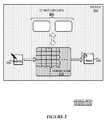
- FIG. 2is a block diagram of a device having a hybrid Non-Volatile Memory (NVM) circuit according to embodiments, for storing data to be used by other components of the device;
- NVMNon-Volatile Memory
- FIG. 3is a block diagram of a device having a particular embodiment of the hybrid NVM circuit of FIG. 2 that accommodates two different types of NVM subcircuits, for storing data to be used by other components of the device;
- FIG. 4is a block diagram of a device having a particular embodiment of the hybrid NVM circuit of FIG. 2 that accommodates three different types of NVM subcircuits, for storing data to be used by other components of the device;
- FIG. 5Ais a block diagram illustrating an implementation of the hybrid NVM circuit of FIG. 4 according to an embodiment
- FIG. 5Bis a block diagram illustrating an implementation of the hybrid NVM circuit of FIG. 4 according to another embodiment
- FIG. 6schematically illustrates an embodiment of an ordinary type of NVM cell that may be part of the hybrid NVM circuit of FIG. 3 or FIG. 4 ;
- FIG. 7schematically illustrates an embodiment of another type of NVM cell that may be part of the hybrid NVM circuit of FIG. 3 or FIG. 4 ;
- FIG. 8schematically illustrates an embodiment of yet another type of an NVM cell that may be part of the hybrid NVM circuit of FIG. 3 or FIG. 4 ;
- FIG. 9schematically illustrates an embodiment of one more type of an NVM cell that may be part of the hybrid NVM circuit of FIG. 3 or FIG. 4 .
- the meaning of “a,” “an,” and “the”includes plural reference, the meaning of “in” includes “in” and “on.”
- the term “connected”means a direct electrical connection between the items connected, without any intermediate devices.
- the term “coupled”means either a direct electrical connection between the items connected or an indirect connection through one or more passive or active intermediary devices.
- the term “circuit”means either a single component or a multiplicity of components, either active and/or passive, that are coupled together to provide a desired function.
- signalmeans at least one current, voltage, charge, temperature, data, or other measurable quantity.
- ordinary NVMrefers to an NVM circuit or device that stores and outputs a logic value to be used by an operational component. As such, the “ordinary NVM” may or may not be arranged to provide the logic value for special purposes such as trimming an analog circuit.
- FIG. 1Ais a block diagram of device 102 A that includes a programmable fuse block for storing data such as calibration data to be used by an operational component.
- Device 102 Aincludes programmable fuse block 112 , operational component 108 , and controller 122 .
- Device 102 Amay be any electronic device that uses a memory circuit, in particular, a non-volatile memory circuit.
- Device 102 Amay use a variety of NVM circuits depending on available power, size, use of the stored information, and the like.
- device 102 Amay be a Radio Frequency IDentification (RFID) tag with limitations on available power and size that uses an output of its NVM circuit to calibrate certain operational components, and the like.
- RFIDRadio Frequency IDentification
- a programmable fuseis essentially a non-volatile memory because it retains stored information in a power off state.
- a programmable fusemay be one time programmable (OTP) or multiple times programmable (MTP).
- Programmable fuse block 112 shown in the figuremay include one or more programmable fuses. In case of multiple fuses, programmable fuse block 112 may include fuses that are arranged in an array.
- Programmable fuse block 112may provide an output to operational component 108 immediately following a transition to power-on state, while other types of NVM circuits may need to be addressed prior to providing their output. Accordingly, programmable fuse block 112 provides a fast NVM circuit that may be employed to calibrate operational components of a device during a power-on mode.
- Device 102 Aalso includes an operational component 108 .
- operational component 108is intended to be any one or more of a large possible number of components of device 102 A, including programmable fuse block 112 itself, or even a component external to device 102 A.
- Operational component 108may operate based on configuration/calibration data. A number of ways for accomplishing this are described later in this document. A distinction should be kept in mind, however, that programmable fuse block 112 may be employed to store other types of data in addition to the calibration data, such as a serial number of the RFID tag.
- Programmable fuse blockcan store data 133 in cell 132 .
- Data 133encodes at least one value, or a series of values, for one or more operational components such as operational component 108 .
- Data 133may be the calibration data for operational component 108 .
- Cell 132may be a programmable fuse, a group of fuses, and the like.
- Data 133encodes at least one value, or a series of values, for one or more operational components such as operational component 108 .
- data 133is at least one logical bit, such as a 1 or a zero, stored in cell 132 .
- Data 133may be input in operational component 108 via any number of paths. As data 133 is moved, it may change nature, or what it encodes.
- Device 102 Amoreover includes controller 122 .
- Controller 122is adapted to program data 133 in cell 132 .
- controller 122may cooperate with other components, such as operational component 108 .
- operational component 108may be any one or more of any of the tag circuit components. If more than one, then a plurality of calibration data may be stored. For each one of the possible operational components, one or more of their operation or performance characteristics may be controlled and/or changed by the calibration data. A number of examples and manners of controlling are described in this document.
- FIG. 1Bis a block diagram of device 102 B that includes an ordinary NVM circuit for storing data such as calibration data to be used by another operational component.
- Device 102 Bincludes NVM circuit 114 , operational component 109 , and controller 124 . Parts of device 102 B perform actions that are similar to the actions performed by comparable parts in device 102 A of FIG. 1A , while each part may or may not be formed and function similarly as described below.
- NVM circuit 114is an ordinary NVM circuit that is arranged to store data 135 , a logic or non-logic value, such as an ON/OFF state, in individual cells (e.g. cell 134 ) and provide data 135 upon being addressed.
- NVM circuit 114may be an NVM array comprising cells that are addressable in terms of a row and a column.
- a value for data 135may be encoded in an amount of charge stored in a device.
- data 135may be at least one logical bit, such as a 1 or a zero, stored in cell 134 .
- data 135may need more than one cell, and so on.
- Controller 124is adapted to program data 135 in cell 134 . Controller 124 is also arranged to address cell 134 to provide data 135 to operational component 109 . In addition, controller 124 may cooperate with other components, such as operational component 109 .
- Operational component 109may be adapted to receive data 135 for processing, calibration, and the like.
- data 135is input in operational component 109 directly.
- data 135may be routed through any suitable component before being input in operational component 109 .
- data 135may be first input from cell 134 into a binary output circuit. Then, from the binary output circuit, data 135 may be input in operational component 109 .
- controller 124may be adapted to sense a performance of operational component 109 . Controller 109 may then determine data 135 so as to adjust the performance. The performance may be optimized, if needed. In some instances, adjusting can be to diminish the performance if, for example, more privacy is required.
- This feature of determining what data 135 to programmay be invoked spontaneously, autonomously, in response to a received command, and so on. Adjusting may be desired if the performance has changed, for example either due to the passage of time, or due to changed environmental conditions, and so on. Adjusting may also take place while manufacturing or testing a device, or preparing it for field use. For example, the processor may step through a number of values to adjust an antenna reception of an RFID tag.
- Device 102 Bmay be implemented with fewer or additional components such as support circuitry for NVM circuit 114 , communication circuitry for interaction with other devices, and the like.
- FIG. 1Cis a block diagram of device 102 C that includes a programmable fuse block such as that of FIG. 1A , and an ordinary NVM circuit such as that of FIG. 1B for storing data to be used by different operational components.
- Parts of device 102 C that are similarly numbered in FIGS. 1A and 1Bperform actions that are similar to the actions performed by comparable parts in devices 102 A and 102 B.
- programmable fuse block 112is adapted to provide a fast calibration data (e.g. data 133 ) to operational component 108 , while NVM circuit 114 is adapted to provide data 135 to operational component 109 for programming purposes, and the like, upon being addressed.
- a fast calibration datae.g. data 133
- NVM circuit 114is adapted to provide data 135 to operational component 109 for programming purposes, and the like, upon being addressed.
- Controller 126may be a combination of controllers 122 and 124 of FIGS. 1A and 1B , and manage programmable fuse block 112 and NVM circuit 114 . Consequently, controller 126 may include different blocks to address, program, monitor, and the like, programmable fuse block 112 and NVM circuit 114 .
- RFID tagsmay include components that need calibration data at power-on and other components that need programming data after power-on.
- having separate controller sub-circuits for different types of memory circuitsis likely to increase power consumption and size of circuitry.
- applications like RFID tagsavailable power and size are at a premium.
- FIG. 2is a block diagram of device 202 having a hybrid Non-Volatile Memory (NVM) circuit according to embodiments, for storing data to be used by other components of the device.
- NVMNon-Volatile Memory
- Device 202includes hybrid NVM circuit 210 that is adapted to interact with other circuits 204 .
- Individual cells of hybrid NVM 210are adapted to store information as a result of “write” operation 206 and provide the stored information as a result of “read” operation 208 . The information is stored even during a power-off state of device 202 .
- “Read” operation 208which provides the stored information to one or more of the other circuits 204 , may occur during a transition from the power-off state to a power-on state for some parts of hybrid NVM circuit 210 .
- “read” operation 208may occur during the power-on state upon being addressed by another circuit (e.g. a controller).
- different circuits of device 202may receive data for their operation at different states of powering the device.
- an oscillator circuitmay be provided calibration data during the transition from the power-off state from one part of hybrid NVM circuit 210
- a digital signal processor circuitmay be provided programming data after the transition.
- hybrid NVM circuit 210may include analog, digital or other types of data.
- different parts of hybrid NVM circuit 210may provide logic bits, ON/OFF states, latched outputs for trimming analog circuits, and the like.
- FIG. 3is a block diagram of device 300 having a particular embodiment of the hybrid NVM circuit 210 of FIG. 2 that accommodates two different types of NVM sub-circuits, for storing data to be used by other components of the device.
- Hybrid NVM circuit 310includes first type NVM sub-circuit 312 and second type NVM sub-circuit 314 .
- First type NVM sub-circuit 312 and second type NVM sub-circuit 314operate as described previously and provide input to operational components 307 and 308 , respectively.
- first type NVM sub-circuit 312may provide a fast output for calibrating operational component 307 during a transition to the power-on state.
- second type NVM sub-circuit 314may provide programming data to operational component 308 in the power-on state upon being addressed by controller 320 .
- Controller 320is adapted to interact with both NVM sub-circuits. The interaction may include programming the NVM sub-circuits, addressing individual cells to output their data, and the like.
- hybrid NVM circuit 310may also include a sub-circuit that is adapted to store one or more fixed bits.
- controller 320may include a by-passing circuit that arranged to by-pass the one or more fixed bits. Such a by-passing circuit may also include at least one programmable bit.
- first type NVM sub-circuit 312 and second type NVM sub-circuit 314By integrating first type NVM sub-circuit 312 and second type NVM sub-circuit 314 , and combining the control operations in a single controller ( 320 ), size and power consumption can be optimized.
- FIG. 4is a block diagram of device 400 having a particular embodiment of the hybrid NVM circuit 210 of FIG. 2 that accommodates three different types of NVM subcircuits, for storing data to be used by other components of the device.
- hybrid NVM circuit 410includes three NVM sub-circuits: first type NVM sub-circuit 312 , second type NVM sub-circuit 314 , third type NVM sub-circuit 416 .
- third type NVM sub-circuit 416provides input to operational component 409 .
- third type NVM sub-circuit 416may provide a latched output for trimming an analog circuit.
- third type NVM sub-circuit 416may provide an ON/OFF state output that may be employed to control at least one of a voltage, a frequency, or a current.
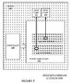
- FIG. 5Ais a block diagram illustrating an implementation of hybrid NVM circuit 510 A according to an embodiment.
- Hybrid NVM circuit 510 Aincludes first type NVM sub-circuit 512 , second type NVM sub-circuit 514 , and third type NVM sub-circuit 516 . These NVM sub-circuits are examples of NVM circuits as described in conjunction with previous figures.
- NVM sub-circuitscommonly comprise a number of cells (e.g. cells 532 , 534 , and 536 ), which store the data to be consumed by operational components.
- NVM sub-circuitsmay be implemented in form of an NVM array comprising cells that are addressable in terms of a row and a column.
- First type NVM sub-circuit 512 and second type NVM sub-circuit 514are examples of NVM arrays, while third type NVM sub-circuit 516 illustrates a non-array NVM circuit.
- a non-volatile memory cellmay be constructed using a floating-gate pFET readout transistor having its source tied to a power source and its drain providing a current, which can be sensed to determine the state of the cell.
- the gate of the pFET readout transistorprovides for charge storage, which can be used to represent information such as binary bits.
- a control capacitor structurehaving its first terminal coupled to a first voltage source and its second terminal coupled to the floating gate and a tunneling capacitor structure having its first terminal coupled to a second voltage source and its second terminal coupled to the floating gate may be utilized in each embodiment.
- the control capacitor structureis fabricated so that it has much more capacitance than does the tunneling capacitor structure (and assorted stray capacitance between the floating gate and various other nodes of the cell). Manipulation of the voltages applied to the first voltage source and second voltage source controls an electric field across the capacitor structure and pFET dielectrics and thus Fowler-Nordheim tunneling of electrons onto and off of the floating gate, thus controlling the charge on the floating gate and the information value stored thereon.
- High voltage switches 541 and 542are examples of a series of high voltage switches that are arranged to provide the first and the second voltages for programming and erasing of the NVM cells.
- NVM controller 546is arranged to program and address individual cells of the NVM sub-circuits to output their data by managing high voltage switches 541 , 542 , and the like.
- NVM charge pump 545is an electronic circuit that uses capacitors as energy storage elements to convert low voltages into higher voltage outputs. Charge pump circuits are typically capable of high efficiencies, sometimes as high as 90-95%.
- NVM charge pump 545may use switches to control a connection of voltages to the capacitor. For example, to generate a higher voltage, a first stage may involve the capacitor being connected across a voltage and charged up. In a second stage, the capacitor is disconnected from the original charging voltage and reconnected with its negative terminal to the original positive charging voltage. Because the capacitor retains the voltage across it (ignoring leakage effects) the positive terminal voltage is added to the original, effectively doubling the voltage. This higher voltage output may then be smoothed by the use of another capacitor.
- FIG. 5Bis a block diagram illustrating an implementation of hybrid NVM circuit 510 B according to another embodiment. Parts of hybrid NVM circuit 510 B that are similarly numbered in hybrid NVM circuit 510 A of FIG. 5A operate in a likewise manner.
- hybrid NVM circuit 510 Bincludes CLOOP 548 in place of high voltage switch 542 .
- a Control Loop for Overtunneling Current Prevention (CLOOP) devicemay be implemented instead of a series of high voltage switches that control rows and columns of NVM arrays within the hybrid NVM circuit.
- CLOOP 548is such a device. Structure and operation of a CLOOP device is described in detail in U.S. Pat. No. 6,853,583.
- FIGS. 5A and 5Bare for illustration purposes, and do not constitute a limitation on the present invention.
- Other embodimentsmay be implemented using other circuits and other combinations of circuits for providing common support circuitry to a plurality of NVM sub-circuits of a hybrid NVM circuit, without departing from the scope and spirit of the invention.
- the hybrid NVM circuitmay further include an oscillator, an ESD protection device, and the like.
- FIG. 6schematically illustrates an embodiment of an ordinary type of NVM cell ( 634 ) that may be part of the hybrid NVM circuit of FIG. 3 or FIG. 4 .
- NVM cell 634is adapted to store and provide a logic value such as a “1” or a “0” bit. While FIG. 6 shows an example implementation, an “ordinary” NVM cell may be implemented in any way known in the art.
- NVM cell 634shows the tunneling transistors as capacitors denoted CG 1 and CG 0 and the control transistors as capacitors denoted CG 1 ′ and CG 0 ′ for clarity but they may be implemented with pFETs, for example as described in U.S. patent application Ser. No. 11/839,935 (IMPJ-0057) filed on May 5, 2004.
- VDDmay be provided at all times to bias the gates of transistors M 1 C and M 0 C.
- RENrow enable
- RSBrow select bar
- TUNis tunneling signal provided to tunneling capacitors CG 1 and CG 0 .
- the signals VDD, REN, TUN and RSBare the row control signals, although VDD need not be applied via a row and could instead be applied via a column.
- the column control signalscomprise the data signals on lines D 1 and D 0 .
- Transistors M 1 C and M 0 Chave their gates coupled together and to VDD and their sources, drains and well connections coupled to the corresponding sources, drains and well connections of respective readout transistors M 1 A and M 0 A. This is done in order to avoid disturbing the contents of the cell when it is not selected.
- the REN (row enable) lineis set to VDD and with the gates of M 1 C and M 0 C at VDD.
- M 1 C and M 0 Care not conducting and readout transistors M 1 A and M 0 A operate normally to provide an output current as a function of charge stored on corresponding floating gates FG 1 and FG 0 .
- RENis set to approximately half the tunneling voltage.
- VDDvoltage on the gates of M 1 C and M 0 C
- M 1 C and M 0 Cconduct, effectively connecting the drain nodes of M 1 A and M 0 A to REN. Since the drain, source, and bulk nodes of both M 1 A and M 0 A are set to half the tunneling voltage, there can be no tunneling across M 1 A or M 0 A.
- TUNis also set to half the tunneling voltage during the write mode. Accordingly, there can be no tunneling across CG 1 or CG 0 .
- FIG. 7schematically illustrates an embodiment of another type of NVM cell ( 732 ) that may be part of the hybrid NVM circuit of FIG. 3 or FIG. 4 .
- NVM cell 732is one embodiment of a programmable fuse implemented using Metal Oxide Field Effect Transistors (MOSFETs).
- NVM cell 732comprises cross-coupled transistor pair M 1 C and M 0 B, which form a half latch circuit.
- M 1 C and M 0 Bmay be nFETs.
- a gate terminal of M 1 Cis coupled to a drain of M 0 B.
- a gate terminal of M 0 Bis coupled to a drain of M 1 C. Sources of both transistors are coupled together and are arranged to receive a ground signal.
- the drain terminal of M 0 Bis arranged to provide output signal OUT, which includes stored value 733 .
- stored value 733may be a digital value “0” or “1”.
- Drain terminals of pFET type transistors M 1 A and M 0 Care coupled to drain terminals of M 1 C and M 0 B, respectively.
- Source terminals of M 1 A and M 0 Care coupled to a supply voltage (VDD).
- the source terminalsare also arranged to receive a reset signal or a power-on reset (POR) signal.
- Gate terminals of M 1 A and M 0 Care arranged as floating gates that store a charge such that NVM cell 732 settles on a state determined by the charges of the floating gates upon receiving a power-up signal (VDD applied) or the reset signal.
- CMOScomplementary metal-oxide-semiconductor
- CMOScomplementary metal-oxide-semiconductor
- transistorsare not restricted to MOSFET type transistors, and other types devices may also be employed.
- the programmable fuse forming NVM cell 732is termed “self-latching”, meaning that once power is applied to the fuse, the latch of the associated fuse will eventually settle to some state. Details of programmable fuses are described in more detail in U.S. patent application Ser. No. 10/813,907 (IMPJ-0027A) filed on Mar. 30, 2004; Ser. No. 10/814,866 (IMPJ-0027B) filed on Mar. 30, 2004; and Ser. No. 10/814,868 (IMPJ-0027C) filed on Mar. 30, 2004.
- FIG. 8schematically illustrates an embodiment of yet another type of an NVM cell ( 836 ) that may be part of the hybrid NVM circuit of FIG. 3 or FIG. 4 .
- NVM cell 836provides a latched output to other operational components. This makes an output of NVM cell 836 suitable for trimming analog circuits. Parts of NVM cell 836 that are similarly numbered in NVM cell 634 of FIG. 6 operate in a likewise manner.
- NVM cell 836includes latch 852 , which is coupled to drains of M 1 B and M 0 B. Sources of M 1 B and M 0 B are coupled to drains of M 1 C-M 1 A and M 0 C-M 0 A transistor pairs. RSB signal controls gate terminals of M 1 B and M 0 B providing an output to latch 852 .
- Latch 852is arranged to settle on a state upon receiving the output of NVM cell 634 such that the stored output can be used to trim an analog circuit, and the like.
- FIG. 9schematically illustrates an embodiment of one more type of an NVM cell ( 938 ) that may be part of the hybrid NVM circuit of FIG. 3 or FIG. 4 .
- NVM cell 938includes transistors M 1 A and M 1 C, which are coupled together at their source and drain terminals.
- the source terminalsare arranged to receive REN signal, while the drain terminals are arranged to provide an output.
- a gate terminal of M 1 Cis arranged to receive supply voltage VDD.
- a tunneling transistor as capacitor denoted CG 1 and a control transistor as capacitor denoted CG 1 ′are coupled to a gate terminal of M 1 A, and function as described above in conjunction with FIG. 6 .
- An output of NVM cell 938may be an ON state of an OFF state.
- the outputmay be used to control a current, a voltage, or a frequency of an operational component.
Landscapes
- Engineering & Computer Science (AREA)
- Microelectronics & Electronic Packaging (AREA)
- Computer Hardware Design (AREA)
- Semiconductor Integrated Circuits (AREA)
- Read Only Memory (AREA)
Abstract
Description
Claims (27)
Priority Applications (1)
| Application Number | Priority Date | Filing Date | Title |
|---|---|---|---|
| US11/829,370US8077511B2 (en) | 2004-04-21 | 2007-07-27 | Hybrid non-volatile memory |
Applications Claiming Priority (6)
| Application Number | Priority Date | Filing Date | Title |
|---|---|---|---|
| US10/830,280US7212446B2 (en) | 2002-09-16 | 2004-04-21 | Counteracting overtunneling in nonvolatile memory cells using charge extraction control |
| US10/839,985US7221596B2 (en) | 2002-07-05 | 2004-05-05 | pFET nonvolatile memory |
| US11/015,293US20060133140A1 (en) | 2004-12-17 | 2004-12-17 | RFID tags storing component configuration data in non-volatile memory and methods |
| US11/016,546US7307529B2 (en) | 2004-12-17 | 2004-12-17 | RFID tags with electronic fuses for storing component configuration data |
| US11/237,099US7283390B2 (en) | 2004-04-21 | 2005-09-28 | Hybrid non-volatile memory |
| US11/829,370US8077511B2 (en) | 2004-04-21 | 2007-07-27 | Hybrid non-volatile memory |
Related Parent Applications (1)
| Application Number | Title | Priority Date | Filing Date |
|---|---|---|---|
| US11/237,099ContinuationUS7283390B2 (en) | 2004-04-21 | 2005-09-28 | Hybrid non-volatile memory |
Publications (2)
| Publication Number | Publication Date |
|---|---|
| US20080205150A1 US20080205150A1 (en) | 2008-08-28 |
| US8077511B2true US8077511B2 (en) | 2011-12-13 |
Family
ID=44141219
Family Applications (2)
| Application Number | Title | Priority Date | Filing Date |
|---|---|---|---|
| US11/237,099Expired - LifetimeUS7283390B2 (en) | 2004-04-21 | 2005-09-28 | Hybrid non-volatile memory |
| US11/829,370Expired - LifetimeUS8077511B2 (en) | 2004-04-21 | 2007-07-27 | Hybrid non-volatile memory |
Family Applications Before (1)
| Application Number | Title | Priority Date | Filing Date |
|---|---|---|---|
| US11/237,099Expired - LifetimeUS7283390B2 (en) | 2004-04-21 | 2005-09-28 | Hybrid non-volatile memory |
Country Status (1)
| Country | Link |
|---|---|
| US (2) | US7283390B2 (en) |
Cited By (3)
| Publication number | Priority date | Publication date | Assignee | Title |
|---|---|---|---|---|
| US9508396B2 (en) | 2014-04-02 | 2016-11-29 | Ememory Technology Inc. | Array structure of single-ploy nonvolatile memory |
| US10373694B2 (en)* | 2017-08-31 | 2019-08-06 | Micron Technology, Inc. | Responding to power loss |
| US10388388B2 (en) | 2017-08-31 | 2019-08-20 | Micron Technology, Inc. | Responding to power loss |
Families Citing this family (25)
| Publication number | Priority date | Publication date | Assignee | Title |
|---|---|---|---|---|
| US7283390B2 (en)* | 2004-04-21 | 2007-10-16 | Impinj, Inc. | Hybrid non-volatile memory |
| US8111558B2 (en)* | 2004-05-05 | 2012-02-07 | Synopsys, Inc. | pFET nonvolatile memory |
| US7257033B2 (en) | 2005-03-17 | 2007-08-14 | Impinj, Inc. | Inverter non-volatile memory cell and array system |
| US7679957B2 (en) | 2005-03-31 | 2010-03-16 | Virage Logic Corporation | Redundant non-volatile memory cell |
| JP2007042204A (en)* | 2005-08-02 | 2007-02-15 | Sony Corp | Reproducing apparatus, time limit notification method, and time limit notification program |
| US7257023B2 (en)* | 2005-08-10 | 2007-08-14 | Taiwan Semiconductor Manufacturing Co. | Hybrid non-volatile memory device |
| US20070247915A1 (en)* | 2006-04-21 | 2007-10-25 | Intersil Americas Inc. | Multiple time programmable (MTP) PMOS floating gate-based non-volatile memory device for a general-purpose CMOS technology with thick gate oxide |
| US8122307B1 (en) | 2006-08-15 | 2012-02-21 | Synopsys, Inc. | One time programmable memory test structures and methods |
| US8054687B2 (en)* | 2007-04-23 | 2011-11-08 | Georgia Tech Research Corporation | Systems and methods of providing programmable voltage and current reference devices |
| US7719896B1 (en) | 2007-04-24 | 2010-05-18 | Virage Logic Corporation | Configurable single bit/dual bits memory |
| US7903465B2 (en)* | 2007-04-24 | 2011-03-08 | Intersil Americas Inc. | Memory array of floating gate-based non-volatile memory cells |
| US7688627B2 (en)* | 2007-04-24 | 2010-03-30 | Intersil Americas Inc. | Flash memory array of floating gate-based non-volatile memory cells |
| US7920423B1 (en)* | 2007-07-31 | 2011-04-05 | Synopsys, Inc. | Non volatile memory circuit with tailored reliability |
| US7894261B1 (en) | 2008-05-22 | 2011-02-22 | Synopsys, Inc. | PFET nonvolatile memory |
| US7750694B1 (en)* | 2008-11-11 | 2010-07-06 | Altera Corporation | Power on reset circuitry for manufacturability and security using a fuse |
| US8169321B2 (en)* | 2010-01-29 | 2012-05-01 | International Business Machines Corporation | Radio frequency-enabled electromigration fuse |
| US8690057B2 (en) | 2012-03-06 | 2014-04-08 | A-I Packaging Solutions, Inc. | Radio frequency identification system for tracking and managing materials in a manufacturing process |
| CN106062724B (en)* | 2013-09-27 | 2020-09-08 | 慧与发展有限责任合伙企业 | Method for managing data on memory module, memory module and storage medium |
| CN107847323B (en)* | 2015-06-01 | 2020-04-24 | 爱德华兹生命科学公司 | Heart valve repair device configured for percutaneous delivery |
| US10319444B2 (en) | 2017-10-30 | 2019-06-11 | International Business Machines Corporation | Memory data randomizer |
| US11348067B2 (en) | 2018-03-30 | 2022-05-31 | A-1 Packaging Solutions, Inc. | RFID-based inventory tracking system |
| US11023851B2 (en) | 2018-03-30 | 2021-06-01 | A-1 Packaging Solutions, Inc. | RFID-based inventory tracking system |
| CA3134716A1 (en) | 2019-04-22 | 2020-10-29 | Kenneth F. Schoening | Rfid-based inventory tracking system |
| US11270780B2 (en) | 2020-03-31 | 2022-03-08 | Taiwan Semiconductor Manufacturing Co., Ltd. | Memory readout circuit and method |
| US11250922B2 (en) | 2020-04-20 | 2022-02-15 | AP Memory Technology Corp. | Memory cell, memory device, and related identification tag |
Citations (186)
| Publication number | Priority date | Publication date | Assignee | Title |
|---|---|---|---|---|
| US4090258A (en) | 1976-12-29 | 1978-05-16 | Westinghouse Electric Corp. | MNOS non-volatile memory with write cycle suppression |
| US4132904A (en) | 1977-07-28 | 1979-01-02 | Hughes Aircraft Company | Volatile/non-volatile logic latch circuit |
| US4158239A (en) | 1977-12-20 | 1979-06-12 | International Business Machines Corporation | Resistive gate FET flip-flop storage cell |
| US4384288A (en) | 1980-12-31 | 1983-05-17 | Walton Charles A | Portable radio frequency emitting identifier |
| US4388524A (en) | 1981-09-16 | 1983-06-14 | Walton Charles A | Electronic identification and recognition system with code changeable reactance |
| US4541073A (en) | 1981-11-20 | 1985-09-10 | Societe Pour L'etude Et La Fabrication De Circuits Integres Speciaux | Non-volatile flip-flop with a static resetting |
| US4546241A (en) | 1982-12-10 | 1985-10-08 | Walton Charles A | Electronic proximity identification system |
| US4571704A (en) | 1984-02-17 | 1986-02-18 | Hughes Aircraft Company | Nonvolatile latch |
| US4575823A (en) | 1982-08-17 | 1986-03-11 | Westinghouse Electric Corp. | Electrically alterable non-volatile memory |
| US4580041A (en) | 1983-12-09 | 1986-04-01 | Walton Charles A | Electronic proximity identification system with simplified low power identifier |
| US4758869A (en) | 1986-08-29 | 1988-07-19 | Waferscale Integration, Inc. | Nonvolatile floating gate transistor structure |
| US4935702A (en) | 1988-12-09 | 1990-06-19 | Synaptics, Inc. | Subthreshold CMOS amplifier with offset adaptation |
| US4953928A (en) | 1989-06-09 | 1990-09-04 | Synaptics Inc. | MOS device for long-term learning |
| US5018102A (en) | 1988-12-20 | 1991-05-21 | Texas Instruments, Incorporated | Memory having selected state on power-up |
| US5068622A (en) | 1988-12-09 | 1991-11-26 | Synaptics, Incorporated | CMOS amplifier with offset adaptation |
| US5086331A (en) | 1988-04-05 | 1992-02-04 | U.S. Philips Corp. | Integrated circuit comprising a programmable cell |
| US5124568A (en) | 1991-02-14 | 1992-06-23 | Advanced Micro Devices, Inc. | Edge-triggered flip-flop |
| US5146106A (en) | 1988-12-09 | 1992-09-08 | Synaptics, Incorporated | CMOS winner-take all circuit with offset adaptation |
| US5168464A (en) | 1989-11-29 | 1992-12-01 | Ncr Corporation | Nonvolatile differential memory device and method |
| EP0298618B1 (en) | 1987-07-08 | 1993-10-27 | Tektronix Inc. | Interleaved digitizer array with calibrated sample timing |
| US5272368A (en) | 1991-05-10 | 1993-12-21 | Altera Corporation | Complementary low power non-volatile reconfigurable EEcell |
| US5301150A (en) | 1992-06-22 | 1994-04-05 | Intel Corporation | Flash erasable single poly EPROM device |
| US5323066A (en) | 1992-06-01 | 1994-06-21 | Motorola, Inc. | Method and apparatus for performing power on reset initialization in a data processing system |
| US5361001A (en) | 1993-12-03 | 1994-11-01 | Motorola, Inc. | Circuit and method of previewing analog trimming |
| EP0326883B1 (en) | 1988-01-28 | 1994-12-28 | National Semiconductor Corporation | Zero power, electrically alterable, nonvolatile latch |
| US5384727A (en) | 1993-11-08 | 1995-01-24 | Advanced Micro Devices, Inc. | Fuse trimming in plastic package devices |
| US5394367A (en) | 1994-03-18 | 1995-02-28 | Ramtron International Corporation | System and method for write-protecting predetermined portions of a memory array |
| US5430670A (en) | 1993-11-08 | 1995-07-04 | Elantec, Inc. | Differential analog memory cell and method for adjusting same |
| US5438542A (en) | 1993-05-28 | 1995-08-01 | Kabushiki Kaisha Toshiba | Nonvolatile semiconductor memory device |
| US5463348A (en) | 1994-07-27 | 1995-10-31 | California Institute Of Technology | CMOS low-power, wide-linear-range, well-input differential and transconductance amplifiers |
| US5504707A (en)* | 1993-09-17 | 1996-04-02 | Fujitsu Limited | Semiconductor device |
| US5517044A (en) | 1992-02-07 | 1996-05-14 | Nec Corporation | Non-volatile semiconductor memory device having thin film transistors equipped with floating gates |
| US5541878A (en) | 1991-05-09 | 1996-07-30 | Synaptics, Incorporated | Writable analog reference voltage storage device |
| US5596524A (en) | 1995-04-21 | 1997-01-21 | Advanced Micro Devices, Inc. | CMOS memory cell with gate oxide of both NMOS and PMOS transistors as tunneling window for program and erase |
| US5616942A (en) | 1995-03-28 | 1997-04-01 | Hyundai Electronics Industries Co., Ltd. | Flash EEPROM cell and manufacturing methods thereof |
| US5617358A (en) | 1994-03-11 | 1997-04-01 | Nec Corporation | Nonvolatile semiconductor memory device capable of converging threshold voltage with low power supply voltage |
| US5623442A (en) | 1993-07-13 | 1997-04-22 | Nkk Corporation | Memory cells and memory devices with a storage capacitor of parasitic capacitance and information storing method using the same |
| US5627392A (en) | 1995-03-07 | 1997-05-06 | California Institute Of Technology | Semiconductor structure for long term learning |
| US5633518A (en) | 1995-07-28 | 1997-05-27 | Zycad Corporation | Nonvolatile reprogrammable interconnect cell with FN tunneling and programming method thereof |
| JPH09181204A (en) | 1995-11-14 | 1997-07-11 | Programmable Microelectron Corp | PMOS flash memory cell capable of storing multi-level threshold voltage |
| US5650966A (en) | 1995-11-01 | 1997-07-22 | Advanced Micro Devices, Inc. | Temperature compensated reference for overerase correction circuitry in a flash memory |
| US5659498A (en) | 1995-07-28 | 1997-08-19 | Sgs-Thomson Microelectronics S.R.L. | Unbalanced latch and fuse circuit including the same |
| US5677917A (en) | 1996-04-29 | 1997-10-14 | Motorola, Inc. | Integrated circuit memory using fusible links in a scan chain |
| US5687118A (en) | 1995-11-14 | 1997-11-11 | Programmable Microelectronics Corporation | PMOS memory cell with hot electron injection programming and tunnelling erasing |
| US5691939A (en) | 1995-12-07 | 1997-11-25 | Programmable Microelectronics Corporation | Triple poly PMOS flash memory cell |
| US5706227A (en) | 1995-12-07 | 1998-01-06 | Programmable Microelectronics Corporation | Double poly split gate PMOS flash memory cell |
| US5717636A (en) | 1995-05-05 | 1998-02-10 | Sgs-Thomson Microelectronics S.R.L. | EEPROM memory with contactless memory cells |
| US5729155A (en) | 1994-09-21 | 1998-03-17 | Nec Corporation | High voltage CMOS circuit which protects the gate oxides from excessive voltages |
| US5731716A (en) | 1995-01-26 | 1998-03-24 | Sgs-Thomson Microelectronics, S.R.L. | Programmable multibit register for coincidence and jump operations and coincidence fuse cell |
| US5736764A (en) | 1995-11-21 | 1998-04-07 | Programmable Microelectronics Corporation | PMOS flash EEPROM cell with single poly |
| US5754471A (en) | 1995-06-06 | 1998-05-19 | Advanced Micro Devices, Inc. | Low power CMOS array for a PLD with program and erase using controlled avalanche injection |
| US5761121A (en) | 1996-10-31 | 1998-06-02 | Programmable Microelectronics Corporation | PMOS single-poly non-volatile memory structure |
| US5763912A (en) | 1995-09-25 | 1998-06-09 | Intel Corporation | Depletion and enhancement MOSFETs with electrically trimmable threshold voltages |
| US5777926A (en) | 1996-10-24 | 1998-07-07 | Programmable Microelectronics Corporation | Row decoder circuit for PMOS non-volatile memory cell which uses channel hot electrons for programming |
| US5777361A (en) | 1996-06-03 | 1998-07-07 | Motorola, Inc. | Single gate nonvolatile memory cell and method for accessing the same |
| US5786617A (en) | 1994-04-01 | 1998-07-28 | National Semiconductor Corporation | High voltage charge pump using low voltage type transistors |
| US5790060A (en) | 1996-09-11 | 1998-08-04 | Harris Corporation | Digital-to-analog converter having enhanced current steering and associated method |
| US5796656A (en) | 1997-02-22 | 1998-08-18 | Programmable Microelectronics Corporation | Row decoder circuit for PMOS non-volatile memory cell which uses electron tunneling for programming and erasing |
| US5798967A (en) | 1997-02-22 | 1998-08-25 | Programmable Microelectronics Corporation | Sensing scheme for non-volatile memories |
| US5801994A (en) | 1997-08-15 | 1998-09-01 | Programmable Microelectronics Corporation | Non-volatile memory array architecture |
| US5822714A (en) | 1997-03-05 | 1998-10-13 | International Business Machines Corporation | Data processing system and method for accessing a plurality of radio frequency identification tags |
| US5825063A (en) | 1995-03-07 | 1998-10-20 | California Institute Of Technology | Three-terminal silicon synaptic device |
| US5835402A (en) | 1997-03-27 | 1998-11-10 | Xilinx, Inc. | Non-volatile storage for standard CMOS integrated circuits |
| US5841165A (en) | 1995-11-21 | 1998-11-24 | Programmable Microelectronics Corporation | PMOS flash EEPROM cell with single poly |
| US5844300A (en) | 1996-09-19 | 1998-12-01 | Intel Corporation | Single poly devices for monitoring the level and polarity of process induced charging in a MOS process |
| US5854762A (en) | 1996-10-30 | 1998-12-29 | Sgs-Thomson Microelectronics, S.R.L. | Protection circuit for redundancy register set-up cells of electrically programmable non-volatile memory devices |
| US5875126A (en) | 1995-09-29 | 1999-02-23 | California Institute Of Technology | Autozeroing floating gate amplifier |
| US5886566A (en) | 1997-08-21 | 1999-03-23 | Integrated Silicon Solution, Inc. | High voltage charge transfer stage |
| US5890199A (en) | 1996-10-21 | 1999-03-30 | Ramtron International Corporation | Data processor incorporating a ferroelectric memory array selectably configurable as read/write and read only memory |
| US5892709A (en) | 1997-05-09 | 1999-04-06 | Motorola, Inc. | Single level gate nonvolatile memory device and method for accessing the same |
| US5892712A (en) | 1996-05-01 | 1999-04-06 | Nvx Corporation | Semiconductor non-volatile latch device including embedded non-volatile elements |
| US5898613A (en) | 1996-07-24 | 1999-04-27 | California Institute Of Technology | pMOS analog EEPROM cell |
| US5901084A (en) | 1997-03-10 | 1999-05-04 | Mitsubishi Denki Kabushiki Kaisha | Nonvolatile semiconductor memory device having floating gate electrode |
| US5912842A (en) | 1995-11-14 | 1999-06-15 | Programmable Microelectronics Corp. | Nonvolatile PMOS two transistor memory cell and array |
| US5912841A (en) | 1996-12-24 | 1999-06-15 | Hyundai Electronics Industries Co., Ltd. | Repair fuse circuit performing complete latch operation using flash memory cell |
| US5912937A (en) | 1997-03-14 | 1999-06-15 | Xilinx, Inc. | CMOS flip-flop having non-volatile storage |
| US5914895A (en) | 1997-09-10 | 1999-06-22 | Cypress Semiconductor Corp. | Non-volatile random access memory and methods for making and configuring same |
| US5939945A (en) | 1996-07-25 | 1999-08-17 | Siemens Aktiengesellschaft | Amplifier with neuron MOS transistors |
| US5966329A (en) | 1997-10-09 | 1999-10-12 | Programmable Microelectronics Corporation | Apparatus and method for programming PMOS memory cells |
| US5969987A (en) | 1995-07-31 | 1999-10-19 | Information Storage Devices, Inc. | Non-volatile electrically alterable semiconductor memory for analog and digital storage |
| US5972804A (en) | 1997-08-05 | 1999-10-26 | Motorola, Inc. | Process for forming a semiconductor device |
| US5982669A (en) | 1998-11-04 | 1999-11-09 | National Semiconductor Corporation | EPROM and flash memory cells with source-side injection |
| US5990512A (en) | 1995-03-07 | 1999-11-23 | California Institute Of Technology | Hole impact ionization mechanism of hot electron injection and four-terminal ρFET semiconductor structure for long-term learning |
| US6011425A (en) | 1996-12-05 | 2000-01-04 | Electronics And Telecommunications Research Institute | CMOS offset trimming circuit and offset generation circuit |
| US6028789A (en) | 1999-06-15 | 2000-02-22 | Vantis Corporation | Zero-power CMOS non-volatile memory cell having an avalanche injection element |
| US6049229A (en) | 1997-10-09 | 2000-04-11 | Pericom Semiconductor Corp. | Self-biasing CMOS PECL receiver with wide common-mode range and multi-level-transmit to binary decoder |
| US6055185A (en) | 1998-04-01 | 2000-04-25 | National Semiconductor Corporation | Single-poly EPROM cell with CMOS compatible programming voltages |
| US6060919A (en) | 1998-12-04 | 2000-05-09 | Ramtron International Corporation | CMOS preferred state power-up latch |
| US6081451A (en) | 1998-04-01 | 2000-06-27 | National Semiconductor Corporation | Memory device that utilizes single-poly EPROM cells with CMOS compatible programming voltages |
| US6111785A (en) | 1998-08-25 | 2000-08-29 | Sharp Kabushiki Kaisha | Nonvolatile semiconductor memory device capable of decreasing layout area for writing defective address |
| EP0776049B1 (en) | 1995-11-21 | 2000-08-30 | Programmable Microelectronics Corporation | PMOS single-poly non-volatile memory structure |
| US6125053A (en) | 1996-07-24 | 2000-09-26 | California Institute Of Technology | Semiconductor structure for long-term learning |
| US6137721A (en) | 1998-04-01 | 2000-10-24 | National Semiconductor Corporation | Memory device having erasable frohmann-bentchkowsky EPROM cells that use a plate-to-floating gate coupled voltage during erasure |
| US6137723A (en) | 1998-04-01 | 2000-10-24 | National Semiconductor Corporation | Memory device having erasable Frohmann-Bentchkowsky EPROM cells that use a well-to-floating gate coupled voltage during erasure |
| US6137722A (en) | 1998-04-01 | 2000-10-24 | National Semiconductor Corporation | Memory array having Frohmann-Bentchkowsky EPROM cells with a reduced number of access transistors |
| US6141247A (en) | 1997-10-24 | 2000-10-31 | Micron Technology, Inc. | Non-volatile data storage unit and method of controlling same |
| US6151238A (en) | 1999-02-23 | 2000-11-21 | Microchip Technology, Inc. | Calibrating functions of an integrated circuit and storing calibration parameters thereof in a programmable fuse array |
| US6166954A (en) | 1999-07-14 | 2000-12-26 | Programmable Microelectronics Corporation | Single poly non-volatile memory having a PMOS write path and an NMOS read path |
| US6166978A (en) | 1997-05-13 | 2000-12-26 | Nippon Steel Corporation | Semiconductor differential amplifier having a gain controlled by a memory transistor |
| US6190968B1 (en) | 1998-11-04 | 2001-02-20 | National Semiconductor Corporation | Method for forming EPROM and flash memory cells with source-side injection |
| US6208557B1 (en) | 1999-05-21 | 2001-03-27 | National Semiconductor Corporation | EPROM and flash memory cells with source-side injection and a gate dielectric that traps hot electrons during programming |
| US6214666B1 (en) | 1998-12-18 | 2001-04-10 | Vantis Corporation | Method of forming a non-volatile memory device |
| WO2001026113A1 (en) | 1999-10-04 | 2001-04-12 | Koninklijke Philips Electronics N.V. | Integrated circuit with a non-volatile mos ram cell |
| US6222771B1 (en) | 2000-01-31 | 2001-04-24 | Eon Silicon Devices, Inc. | Unified program method and circuitry in flash EEPROM |
| US6222765B1 (en) | 2000-02-18 | 2001-04-24 | Silicon Storage Technology, Inc. | Non-volatile flip-flop circuit |
| US6236223B1 (en) | 1998-11-09 | 2001-05-22 | Intermec Ip Corp. | Method and apparatus for wireless radio frequency testing of RFID integrated circuits |
| US6252802B1 (en) | 1996-09-30 | 2001-06-26 | Stmicroelectronics S.R.L. | Floating gate MOS transistor charge injection circuit and computation devices incorporating it |
| US6294427B1 (en) | 1998-02-17 | 2001-09-25 | Seiko Epson Corporation | Non-volatile semiconductor memory device and fabrication method thereof |
| US6294997B1 (en) | 1999-10-04 | 2001-09-25 | Intermec Ip Corp. | RFID tag having timing and environment modules |
| US6294810B1 (en) | 1998-12-22 | 2001-09-25 | Vantis Corporation | EEPROM cell with tunneling at separate edge and channel regions |
| US20010035216A1 (en) | 2000-05-02 | 2001-11-01 | Kyle Charles E. | Valved couplings for RV sewer hose |
| US20010035816A1 (en) | 1994-10-05 | 2001-11-01 | Beigel Michael L. | Universal electronic identification tag |
| US6320788B1 (en) | 1998-09-25 | 2001-11-20 | Sandisk Corporation | Programmable impedance device |
| US6331949B1 (en) | 1999-12-24 | 2001-12-18 | Sharp Kabushiki Kaisha | Circuit for storing and latching defective address data for a nonvolatile semiconductor memory device having redundant function |
| US20020008271A1 (en) | 1999-10-07 | 2002-01-24 | Monolithic System Technology, Inc. | Non-volatile memory system |
| US20020020871A1 (en) | 2000-02-29 | 2002-02-21 | Micron Technology, Inc. | Static NVRAM with ultra thin tunnel oxides |
| US6363011B1 (en) | 1996-05-01 | 2002-03-26 | Cypress Semiconductor Corporation | Semiconductor non-volatile latch device including non-volatile elements |
| US6363006B2 (en) | 2000-02-02 | 2002-03-26 | Hewlett-Packard Company | Asymmetric RAM cell |
| US6384451B1 (en) | 1999-03-24 | 2002-05-07 | John Caywood | Method and apparatus for injecting charge onto the floating gate of a nonvolatile memory cell |
| US6385090B1 (en) | 2001-02-26 | 2002-05-07 | Fujitsu Limited | Semiconductor nonvolatile memory using floating gate |
| US6385000B1 (en) | 1998-08-21 | 2002-05-07 | International Business Machines Corporation | System and method for extending the operating life of a magnetoresistive transducer provided in a disk drive system |
| US6400622B1 (en)* | 2000-10-26 | 2002-06-04 | Matsushita Electric Industrial Co., Ltd. | Semiconductor memory device |
| US6411545B1 (en) | 1999-11-19 | 2002-06-25 | John Millard And Pamela Ann Caywood 1989 Revokable Living Trust | Non-volatile latch |
| US20020122331A1 (en) | 2001-02-27 | 2002-09-05 | Giovanni Santin | Flash cell fuse circuit |
| US6456992B1 (en) | 1995-03-24 | 2002-09-24 | Tadashi Shibata | Semiconductor arithmetic circuit |
| US6469930B1 (en) | 2000-10-30 | 2002-10-22 | Cypress Semiconductor Corporation | Compact nonvolatile circuit having margin testing capability |
| US6469937B2 (en) | 2000-03-02 | 2002-10-22 | Matsushita Electric Industrial Co., Ltd. | Current sense amplifier circuit |
| US6477103B1 (en) | 2001-09-21 | 2002-11-05 | Silicon Storage Technology, Inc. | Reprogrammable fuse and method of operating |
| US6515919B1 (en) | 1998-08-10 | 2003-02-04 | Applied Wireless Identifications Group, Inc. | Radio frequency powered voltage pump for programming EEPROM |
| US6529407B2 (en) | 2000-06-14 | 2003-03-04 | Hitachi, Ltd. | Semiconductor device with improved latch arrangement |
| US6534816B1 (en) | 1999-03-24 | 2003-03-18 | John M. Caywood | Method and apparatus for injecting charge onto the floating gate of a nonvolatile memory cell |
| US6538468B1 (en) | 2000-07-31 | 2003-03-25 | Cypress Semiconductor Corporation | Method and apparatus for multiple boot-up functionalities for a programmable logic device (PLD) |
| US6563731B1 (en) | 2000-06-21 | 2003-05-13 | National Semiconductor Corporation | EEPROM memory cell array embedded on core CMOS |
| US6573765B2 (en) | 2000-12-15 | 2003-06-03 | Micron Technology, Inc. | Input-output buffer circuit and method for avoiding inadvertent conduction of a pull-up transistor |
| US20030123276A1 (en) | 2001-12-28 | 2003-07-03 | Fujitsu Limited | Semiconductor integrated circuit and semiconductor memory |
| US6590825B2 (en) | 2001-11-01 | 2003-07-08 | Silicon Storage Technology, Inc. | Non-volatile flash fuse element |
| US6611463B1 (en) | 2001-11-14 | 2003-08-26 | Lattice Semiconductor Corporation | Zero-power programmable memory cell |
| US20030183871A1 (en) | 2002-03-22 | 2003-10-02 | Dugger Jeffery Don | Floating-gate analog circuit |
| US6633188B1 (en) | 1999-02-12 | 2003-10-14 | Texas Instruments Incorporated | Sense amplifier-based flip-flop with asynchronous set and reset |
| US6641050B2 (en) | 2001-11-06 | 2003-11-04 | International Business Machines Corporation | Secure credit card |
| US20030206437A1 (en) | 1995-03-07 | 2003-11-06 | California Institute Of Technology, A California Non-Profit Corporation | Floating-gate semiconductor structures |
| US6646919B1 (en) | 1997-03-20 | 2003-11-11 | Altera Corporation | Apparatus and method for margin testing single polysilicon EEPROM cells |
| US20030218925A1 (en) | 2002-04-16 | 2003-11-27 | Torjussen Lars Sundell | Methods for storing data in non-volatile memories |
| US20030222309A1 (en) | 2002-06-04 | 2003-12-04 | Anirban Roy | Programmable logic device circuit and method of fabricating same |
| US6661278B1 (en) | 2002-07-08 | 2003-12-09 | Impinj, Inc. | High voltage charge pump circuit |
| US6664909B1 (en) | 2001-08-13 | 2003-12-16 | Impinj, Inc. | Method and apparatus for trimming high-resolution digital-to-analog converter |
| US20040004861A1 (en) | 2002-07-05 | 2004-01-08 | Impinj, Inc. A Delware Corporation | Differential EEPROM using pFET floating gate transistors |
| US6678190B2 (en) | 2002-01-25 | 2004-01-13 | Ememory Technology Inc. | Single poly embedded eprom |
| US20040017295A1 (en) | 1999-12-20 | 2004-01-29 | Dishongh Terrance J. | Electrically modifiable product labeling |
| US20040021166A1 (en) | 2002-05-09 | 2004-02-05 | Impinj, Inc., A Delaware Corporation | Pseudo-nonvolatile direct-tunneling floating-gate device |
| US20040021170A1 (en) | 1999-03-24 | 2004-02-05 | Caywood John M. | Method and apparatus for injecting charge onto the floating gate of a nonvolatile memory cell |
| US6693819B2 (en) | 2002-01-08 | 2004-02-17 | Broadcom Corporation | High voltage switch circuitry |
| US20040037127A1 (en) | 2002-07-05 | 2004-02-26 | Impinj, Inc., A Delaware Corporation | Differential floating gate nonvolatile memories |
| US20040052113A1 (en) | 2002-09-16 | 2004-03-18 | Impinj, Inc., A Delaware Corporation | Method and apparatus for preventing overtunneling in pFET-based nonvolatile memory cells |
| US20040080982A1 (en) | 2002-10-28 | 2004-04-29 | Tower Semiconductor Ltd. | Complementary non-volatile memory cell |
| US6741500B2 (en) | 2002-10-04 | 2004-05-25 | Hpl Technologies, Inc. | One-time-programmable bit cell with latch circuit having selectively programmable floating gate transistors |
| US20040136245A1 (en)* | 2002-10-30 | 2004-07-15 | Hiroshi Makamura | Semiconductor memory |
| US20040195593A1 (en) | 2002-09-16 | 2004-10-07 | Impinj, Inc., A Delaware Corporation | Counteracting overtunneling in nonvolatile memory cells |
| US6822894B1 (en) | 2003-03-25 | 2004-11-23 | Xilinx, Inc. | Single event upset in SRAM cells in FPGAs with leaky gate transistors |
| US20040240278A1 (en) | 2003-05-27 | 2004-12-02 | Brady Philomena Cleopha | Floating-gate reference circuit |
| US20040263319A1 (en) | 2003-06-30 | 2004-12-30 | Nokia Corporation | System and method for supporting multiple reader-tag configurations using multi-mode radio frequency tag |
| US6845029B2 (en) | 2001-02-27 | 2005-01-18 | Micron Technology, Inc. | Flash cell fuse circuit |
| US20050030827A1 (en) | 2002-09-16 | 2005-02-10 | Impinj, Inc., A Delaware Corporation | PMOS memory cell |
| US6898123B2 (en) | 2003-01-07 | 2005-05-24 | Intersil Americas Inc. | Differential dual floating gate circuit and method for programming |
| US6903436B1 (en) | 2004-04-27 | 2005-06-07 | Taiwan Semiconductor Manufacturing Company, Ltd. | Multiple-time programmable electrical fuse utilizing MOS oxide breakdown |
| US6909389B1 (en) | 2002-06-14 | 2005-06-21 | Impinj, Inc. | Method and apparatus for calibration of an array of scaled electronic circuit elements |
| US20050149896A1 (en) | 2004-01-05 | 2005-07-07 | Madurawe Raminda U. | Integrated circuits with RAM and ROM fabrication options |
| US6946892B2 (en) | 2003-01-21 | 2005-09-20 | Oki Electric Industry Co., Ltd. | Level transforming circuit |
| US20050219931A1 (en) | 2004-03-30 | 2005-10-06 | Impinj, Inc., A Delaware Corporation | Rewriteable electronic fuses |
| US6954383B2 (en) | 2002-09-11 | 2005-10-11 | Elan Microelectronics Corporation | On-system programmable and off-system programmable chip |
| US20050251617A1 (en) | 2004-05-07 | 2005-11-10 | Sinclair Alan W | Hybrid non-volatile memory system |
| US7046549B2 (en) | 2003-12-31 | 2006-05-16 | Solid State System Co., Ltd. | Nonvolatile memory structure |
| US20060123186A1 (en) | 2004-12-07 | 2006-06-08 | Hewlett-Packard Development Company, L.P. | Central processor for memory tag |
| US20060133175A1 (en)* | 2004-12-17 | 2006-06-22 | Vadim Gutnik | RFID tags with electronic fuses for storing component configuration data |
| US20060133140A1 (en) | 2004-12-17 | 2006-06-22 | Vadim Gutnik | RFID tags storing component configuration data in non-volatile memory and methods |
| US7106642B2 (en)* | 2004-09-30 | 2006-09-12 | Kabushiki Kaisha Toshiba | Semiconductor integrated circuit device in which a measure to counter soft errors is taken |
| US20060221715A1 (en)* | 2005-03-31 | 2006-10-05 | Impinj, Inc. | Redundant non-volatile memory cell |
| US7177182B2 (en) | 2004-03-30 | 2007-02-13 | Impinj, Inc. | Rewriteable electronic fuses |
| US7221596B2 (en) | 2002-07-05 | 2007-05-22 | Impinj, Inc. | pFET nonvolatile memory |
| US7283390B2 (en)* | 2004-04-21 | 2007-10-16 | Impinj, Inc. | Hybrid non-volatile memory |
| US20070252701A1 (en) | 2006-04-28 | 2007-11-01 | Berry Curtis L | Radio frequency identification (rfid) portal antenna mounting frame |
| US20070263456A1 (en)* | 2005-03-17 | 2007-11-15 | Impinj, Inc. | Inverter non-volatile memory cell and array system |
| US7307534B2 (en)* | 2004-04-21 | 2007-12-11 | Impinj, Inc. | RFID tag using hybrid non-volatile memory |
| US20080112238A1 (en)* | 2006-10-25 | 2008-05-15 | Seon-Taek Kim | Hybrid flash memory device and method for assigning reserved blocks thereof |
| US7388420B2 (en) | 2004-03-30 | 2008-06-17 | Impinj, Inc. | Rewriteable electronic fuses |
| US7483310B1 (en) | 2006-11-02 | 2009-01-27 | National Semiconductor Corporation | System and method for providing high endurance low cost CMOS compatible EEPROM devices |
- 2005
- 2005-09-28USUS11/237,099patent/US7283390B2/ennot_activeExpired - Lifetime
- 2007
- 2007-07-27USUS11/829,370patent/US8077511B2/ennot_activeExpired - Lifetime
Patent Citations (206)
| Publication number | Priority date | Publication date | Assignee | Title |
|---|---|---|---|---|
| US4090258A (en) | 1976-12-29 | 1978-05-16 | Westinghouse Electric Corp. | MNOS non-volatile memory with write cycle suppression |
| US4132904A (en) | 1977-07-28 | 1979-01-02 | Hughes Aircraft Company | Volatile/non-volatile logic latch circuit |
| US4158239A (en) | 1977-12-20 | 1979-06-12 | International Business Machines Corporation | Resistive gate FET flip-flop storage cell |
| US4384288A (en) | 1980-12-31 | 1983-05-17 | Walton Charles A | Portable radio frequency emitting identifier |
| US4388524A (en) | 1981-09-16 | 1983-06-14 | Walton Charles A | Electronic identification and recognition system with code changeable reactance |
| US4541073A (en) | 1981-11-20 | 1985-09-10 | Societe Pour L'etude Et La Fabrication De Circuits Integres Speciaux | Non-volatile flip-flop with a static resetting |
| US4575823A (en) | 1982-08-17 | 1986-03-11 | Westinghouse Electric Corp. | Electrically alterable non-volatile memory |
| US4546241A (en) | 1982-12-10 | 1985-10-08 | Walton Charles A | Electronic proximity identification system |
| US4580041A (en) | 1983-12-09 | 1986-04-01 | Walton Charles A | Electronic proximity identification system with simplified low power identifier |
| US4571704A (en) | 1984-02-17 | 1986-02-18 | Hughes Aircraft Company | Nonvolatile latch |
| US4758869A (en) | 1986-08-29 | 1988-07-19 | Waferscale Integration, Inc. | Nonvolatile floating gate transistor structure |
| EP0298618B1 (en) | 1987-07-08 | 1993-10-27 | Tektronix Inc. | Interleaved digitizer array with calibrated sample timing |
| EP0326883B1 (en) | 1988-01-28 | 1994-12-28 | National Semiconductor Corporation | Zero power, electrically alterable, nonvolatile latch |
| US5086331A (en) | 1988-04-05 | 1992-02-04 | U.S. Philips Corp. | Integrated circuit comprising a programmable cell |
| EP0336500B1 (en) | 1988-04-05 | 1994-06-15 | Koninklijke Philips Electronics N.V. | Integrated circuit comprising a programmable cell |
| US5068622A (en) | 1988-12-09 | 1991-11-26 | Synaptics, Incorporated | CMOS amplifier with offset adaptation |
| US4935702A (en) | 1988-12-09 | 1990-06-19 | Synaptics, Inc. | Subthreshold CMOS amplifier with offset adaptation |
| US5146106A (en) | 1988-12-09 | 1992-09-08 | Synaptics, Incorporated | CMOS winner-take all circuit with offset adaptation |
| US5018102A (en) | 1988-12-20 | 1991-05-21 | Texas Instruments, Incorporated | Memory having selected state on power-up |
| US4953928A (en) | 1989-06-09 | 1990-09-04 | Synaptics Inc. | MOS device for long-term learning |
| US5168464A (en) | 1989-11-29 | 1992-12-01 | Ncr Corporation | Nonvolatile differential memory device and method |
| US5124568A (en) | 1991-02-14 | 1992-06-23 | Advanced Micro Devices, Inc. | Edge-triggered flip-flop |
| US5541878A (en) | 1991-05-09 | 1996-07-30 | Synaptics, Incorporated | Writable analog reference voltage storage device |
| US5272368A (en) | 1991-05-10 | 1993-12-21 | Altera Corporation | Complementary low power non-volatile reconfigurable EEcell |
| US5517044A (en) | 1992-02-07 | 1996-05-14 | Nec Corporation | Non-volatile semiconductor memory device having thin film transistors equipped with floating gates |
| US5323066A (en) | 1992-06-01 | 1994-06-21 | Motorola, Inc. | Method and apparatus for performing power on reset initialization in a data processing system |
| US5301150A (en) | 1992-06-22 | 1994-04-05 | Intel Corporation | Flash erasable single poly EPROM device |
| US5438542A (en) | 1993-05-28 | 1995-08-01 | Kabushiki Kaisha Toshiba | Nonvolatile semiconductor memory device |
| US5623442A (en) | 1993-07-13 | 1997-04-22 | Nkk Corporation | Memory cells and memory devices with a storage capacitor of parasitic capacitance and information storing method using the same |
| US5504707A (en)* | 1993-09-17 | 1996-04-02 | Fujitsu Limited | Semiconductor device |
| US5430670A (en) | 1993-11-08 | 1995-07-04 | Elantec, Inc. | Differential analog memory cell and method for adjusting same |
| US5412594A (en) | 1993-11-08 | 1995-05-02 | Advanced Micro Devices, Inc. | Fuse trimming in plastic package devices |
| US5384727A (en) | 1993-11-08 | 1995-01-24 | Advanced Micro Devices, Inc. | Fuse trimming in plastic package devices |
| US5361001A (en) | 1993-12-03 | 1994-11-01 | Motorola, Inc. | Circuit and method of previewing analog trimming |
| US5617358A (en) | 1994-03-11 | 1997-04-01 | Nec Corporation | Nonvolatile semiconductor memory device capable of converging threshold voltage with low power supply voltage |
| US5394367A (en) | 1994-03-18 | 1995-02-28 | Ramtron International Corporation | System and method for write-protecting predetermined portions of a memory array |
| US5786617A (en) | 1994-04-01 | 1998-07-28 | National Semiconductor Corporation | High voltage charge pump using low voltage type transistors |
| US5463348A (en) | 1994-07-27 | 1995-10-31 | California Institute Of Technology | CMOS low-power, wide-linear-range, well-input differential and transconductance amplifiers |
| US5729155A (en) | 1994-09-21 | 1998-03-17 | Nec Corporation | High voltage CMOS circuit which protects the gate oxides from excessive voltages |
| US20010035816A1 (en) | 1994-10-05 | 2001-11-01 | Beigel Michael L. | Universal electronic identification tag |
| US5731716A (en) | 1995-01-26 | 1998-03-24 | Sgs-Thomson Microelectronics, S.R.L. | Programmable multibit register for coincidence and jump operations and coincidence fuse cell |
| US5825063A (en) | 1995-03-07 | 1998-10-20 | California Institute Of Technology | Three-terminal silicon synaptic device |
| US5990512A (en) | 1995-03-07 | 1999-11-23 | California Institute Of Technology | Hole impact ionization mechanism of hot electron injection and four-terminal ρFET semiconductor structure for long-term learning |
| US5627392A (en) | 1995-03-07 | 1997-05-06 | California Institute Of Technology | Semiconductor structure for long term learning |
| US20030206437A1 (en) | 1995-03-07 | 2003-11-06 | California Institute Of Technology, A California Non-Profit Corporation | Floating-gate semiconductor structures |
| US6452835B1 (en) | 1995-03-07 | 2002-09-17 | California Institute Of Technology | pMos analog EEPROM cell |
| US5914894A (en) | 1995-03-07 | 1999-06-22 | California Institute Of Technology | Method for implementing a learning function |
| US6456992B1 (en) | 1995-03-24 | 2002-09-24 | Tadashi Shibata | Semiconductor arithmetic circuit |
| US5616942A (en) | 1995-03-28 | 1997-04-01 | Hyundai Electronics Industries Co., Ltd. | Flash EEPROM cell and manufacturing methods thereof |
| US5596524A (en) | 1995-04-21 | 1997-01-21 | Advanced Micro Devices, Inc. | CMOS memory cell with gate oxide of both NMOS and PMOS transistors as tunneling window for program and erase |
| US5717636A (en) | 1995-05-05 | 1998-02-10 | Sgs-Thomson Microelectronics S.R.L. | EEPROM memory with contactless memory cells |
| US5754471A (en) | 1995-06-06 | 1998-05-19 | Advanced Micro Devices, Inc. | Low power CMOS array for a PLD with program and erase using controlled avalanche injection |
| JPH11510315A (en) | 1995-07-28 | 1999-09-07 | ゲートフィールド コーポレイション | Nonvolatile programmable interconnect cell with FN tunnel and method of programming the same |
| EP0756379B1 (en) | 1995-07-28 | 2003-09-24 | STMicroelectronics S.r.l. | Unbalanced latch and fuse circuit including the same |
| US5659498A (en) | 1995-07-28 | 1997-08-19 | Sgs-Thomson Microelectronics S.R.L. | Unbalanced latch and fuse circuit including the same |
| US5633518A (en) | 1995-07-28 | 1997-05-27 | Zycad Corporation | Nonvolatile reprogrammable interconnect cell with FN tunneling and programming method thereof |
| US5969987A (en) | 1995-07-31 | 1999-10-19 | Information Storage Devices, Inc. | Non-volatile electrically alterable semiconductor memory for analog and digital storage |
| US5763912A (en) | 1995-09-25 | 1998-06-09 | Intel Corporation | Depletion and enhancement MOSFETs with electrically trimmable threshold voltages |
| US5875126A (en) | 1995-09-29 | 1999-02-23 | California Institute Of Technology | Autozeroing floating gate amplifier |
| US5986927A (en) | 1995-09-29 | 1999-11-16 | California Institute Of Technology | Autozeroing floating-gate amplifier |
| US5650966A (en) | 1995-11-01 | 1997-07-22 | Advanced Micro Devices, Inc. | Temperature compensated reference for overerase correction circuitry in a flash memory |
| US5912842A (en) | 1995-11-14 | 1999-06-15 | Programmable Microelectronics Corp. | Nonvolatile PMOS two transistor memory cell and array |
| US5666307A (en) | 1995-11-14 | 1997-09-09 | Programmable Microelectronics Corporation | PMOS flash memory cell capable of multi-level threshold voltage storage |
| US5687118A (en) | 1995-11-14 | 1997-11-11 | Programmable Microelectronics Corporation | PMOS memory cell with hot electron injection programming and tunnelling erasing |
| JPH09181204A (en) | 1995-11-14 | 1997-07-11 | Programmable Microelectron Corp | PMOS flash memory cell capable of storing multi-level threshold voltage |
| EP0778623B1 (en) | 1995-11-14 | 2001-07-18 | Programmable Microelectronics Corporation | PMOS memory cell with hot electron injection programming and tunnelling erasing |
| EP0776049B1 (en) | 1995-11-21 | 2000-08-30 | Programmable Microelectronics Corporation | PMOS single-poly non-volatile memory structure |
| US5841165A (en) | 1995-11-21 | 1998-11-24 | Programmable Microelectronics Corporation | PMOS flash EEPROM cell with single poly |
| US5736764A (en) | 1995-11-21 | 1998-04-07 | Programmable Microelectronics Corporation | PMOS flash EEPROM cell with single poly |
| US5706227A (en) | 1995-12-07 | 1998-01-06 | Programmable Microelectronics Corporation | Double poly split gate PMOS flash memory cell |
| US5691939A (en) | 1995-12-07 | 1997-11-25 | Programmable Microelectronics Corporation | Triple poly PMOS flash memory cell |
| US5677917A (en) | 1996-04-29 | 1997-10-14 | Motorola, Inc. | Integrated circuit memory using fusible links in a scan chain |
| US5892712A (en) | 1996-05-01 | 1999-04-06 | Nvx Corporation | Semiconductor non-volatile latch device including embedded non-volatile elements |
| US6363011B1 (en) | 1996-05-01 | 2002-03-26 | Cypress Semiconductor Corporation | Semiconductor non-volatile latch device including non-volatile elements |
| US5777361A (en) | 1996-06-03 | 1998-07-07 | Motorola, Inc. | Single gate nonvolatile memory cell and method for accessing the same |
| US5898613A (en) | 1996-07-24 | 1999-04-27 | California Institute Of Technology | pMOS analog EEPROM cell |
| US6125053A (en) | 1996-07-24 | 2000-09-26 | California Institute Of Technology | Semiconductor structure for long-term learning |
| US6144581A (en) | 1996-07-24 | 2000-11-07 | California Institute Of Technology | pMOS EEPROM non-volatile data storage |
| US5939945A (en) | 1996-07-25 | 1999-08-17 | Siemens Aktiengesellschaft | Amplifier with neuron MOS transistors |
| US5790060A (en) | 1996-09-11 | 1998-08-04 | Harris Corporation | Digital-to-analog converter having enhanced current steering and associated method |
| US5844300A (en) | 1996-09-19 | 1998-12-01 | Intel Corporation | Single poly devices for monitoring the level and polarity of process induced charging in a MOS process |
| US6252802B1 (en) | 1996-09-30 | 2001-06-26 | Stmicroelectronics S.R.L. | Floating gate MOS transistor charge injection circuit and computation devices incorporating it |
| US5890199A (en) | 1996-10-21 | 1999-03-30 | Ramtron International Corporation | Data processor incorporating a ferroelectric memory array selectably configurable as read/write and read only memory |
| US5777926A (en) | 1996-10-24 | 1998-07-07 | Programmable Microelectronics Corporation | Row decoder circuit for PMOS non-volatile memory cell which uses channel hot electrons for programming |
| US5854762A (en) | 1996-10-30 | 1998-12-29 | Sgs-Thomson Microelectronics, S.R.L. | Protection circuit for redundancy register set-up cells of electrically programmable non-volatile memory devices |
| US5761121A (en) | 1996-10-31 | 1998-06-02 | Programmable Microelectronics Corporation | PMOS single-poly non-volatile memory structure |
| US6011425A (en) | 1996-12-05 | 2000-01-04 | Electronics And Telecommunications Research Institute | CMOS offset trimming circuit and offset generation circuit |
| US5912841A (en) | 1996-12-24 | 1999-06-15 | Hyundai Electronics Industries Co., Ltd. | Repair fuse circuit performing complete latch operation using flash memory cell |
| US5798967A (en) | 1997-02-22 | 1998-08-25 | Programmable Microelectronics Corporation | Sensing scheme for non-volatile memories |
| US5796656A (en) | 1997-02-22 | 1998-08-18 | Programmable Microelectronics Corporation | Row decoder circuit for PMOS non-volatile memory cell which uses electron tunneling for programming and erasing |
| US5822714A (en) | 1997-03-05 | 1998-10-13 | International Business Machines Corporation | Data processing system and method for accessing a plurality of radio frequency identification tags |
| US5901084A (en) | 1997-03-10 | 1999-05-04 | Mitsubishi Denki Kabushiki Kaisha | Nonvolatile semiconductor memory device having floating gate electrode |
| US5912937A (en) | 1997-03-14 | 1999-06-15 | Xilinx, Inc. | CMOS flip-flop having non-volatile storage |
| US6646919B1 (en) | 1997-03-20 | 2003-11-11 | Altera Corporation | Apparatus and method for margin testing single polysilicon EEPROM cells |
| US5835402A (en) | 1997-03-27 | 1998-11-10 | Xilinx, Inc. | Non-volatile storage for standard CMOS integrated circuits |
| US5892709A (en) | 1997-05-09 | 1999-04-06 | Motorola, Inc. | Single level gate nonvolatile memory device and method for accessing the same |
| US6166978A (en) | 1997-05-13 | 2000-12-26 | Nippon Steel Corporation | Semiconductor differential amplifier having a gain controlled by a memory transistor |
| US5972804A (en) | 1997-08-05 | 1999-10-26 | Motorola, Inc. | Process for forming a semiconductor device |
| US5801994A (en) | 1997-08-15 | 1998-09-01 | Programmable Microelectronics Corporation | Non-volatile memory array architecture |
| US5886566A (en) | 1997-08-21 | 1999-03-23 | Integrated Silicon Solution, Inc. | High voltage charge transfer stage |
| US5914895A (en) | 1997-09-10 | 1999-06-22 | Cypress Semiconductor Corp. | Non-volatile random access memory and methods for making and configuring same |
| US5966329A (en) | 1997-10-09 | 1999-10-12 | Programmable Microelectronics Corporation | Apparatus and method for programming PMOS memory cells |
| US6049229A (en) | 1997-10-09 | 2000-04-11 | Pericom Semiconductor Corp. | Self-biasing CMOS PECL receiver with wide common-mode range and multi-level-transmit to binary decoder |
| US6141247A (en) | 1997-10-24 | 2000-10-31 | Micron Technology, Inc. | Non-volatile data storage unit and method of controlling same |
| US6294427B1 (en) | 1998-02-17 | 2001-09-25 | Seiko Epson Corporation | Non-volatile semiconductor memory device and fabrication method thereof |
| US6081451A (en) | 1998-04-01 | 2000-06-27 | National Semiconductor Corporation | Memory device that utilizes single-poly EPROM cells with CMOS compatible programming voltages |
| US6137723A (en) | 1998-04-01 | 2000-10-24 | National Semiconductor Corporation | Memory device having erasable Frohmann-Bentchkowsky EPROM cells that use a well-to-floating gate coupled voltage during erasure |
| US6137722A (en) | 1998-04-01 | 2000-10-24 | National Semiconductor Corporation | Memory array having Frohmann-Bentchkowsky EPROM cells with a reduced number of access transistors |
| US6055185A (en) | 1998-04-01 | 2000-04-25 | National Semiconductor Corporation | Single-poly EPROM cell with CMOS compatible programming voltages |
| US6137724A (en) | 1998-04-01 | 2000-10-24 | National Semiconductor Corporation | Memory device that utilizes single-poly EPROM cells with CMOS compatible programming voltages |
| US6137721A (en) | 1998-04-01 | 2000-10-24 | National Semiconductor Corporation | Memory device having erasable frohmann-bentchkowsky EPROM cells that use a plate-to-floating gate coupled voltage during erasure |
| US6515919B1 (en) | 1998-08-10 | 2003-02-04 | Applied Wireless Identifications Group, Inc. | Radio frequency powered voltage pump for programming EEPROM |
| US6385000B1 (en) | 1998-08-21 | 2002-05-07 | International Business Machines Corporation | System and method for extending the operating life of a magnetoresistive transducer provided in a disk drive system |
| US6111785A (en) | 1998-08-25 | 2000-08-29 | Sharp Kabushiki Kaisha | Nonvolatile semiconductor memory device capable of decreasing layout area for writing defective address |
| US6320788B1 (en) | 1998-09-25 | 2001-11-20 | Sandisk Corporation | Programmable impedance device |
| US5982669A (en) | 1998-11-04 | 1999-11-09 | National Semiconductor Corporation | EPROM and flash memory cells with source-side injection |
| US6190968B1 (en) | 1998-11-04 | 2001-02-20 | National Semiconductor Corporation | Method for forming EPROM and flash memory cells with source-side injection |
| US6236223B1 (en) | 1998-11-09 | 2001-05-22 | Intermec Ip Corp. | Method and apparatus for wireless radio frequency testing of RFID integrated circuits |
| US6060919A (en) | 1998-12-04 | 2000-05-09 | Ramtron International Corporation | CMOS preferred state power-up latch |
| US6214666B1 (en) | 1998-12-18 | 2001-04-10 | Vantis Corporation | Method of forming a non-volatile memory device |
| US6294810B1 (en) | 1998-12-22 | 2001-09-25 | Vantis Corporation | EEPROM cell with tunneling at separate edge and channel regions |
| US6633188B1 (en) | 1999-02-12 | 2003-10-14 | Texas Instruments Incorporated | Sense amplifier-based flip-flop with asynchronous set and reset |
| US6151238A (en) | 1999-02-23 | 2000-11-21 | Microchip Technology, Inc. | Calibrating functions of an integrated circuit and storing calibration parameters thereof in a programmable fuse array |
| US6534816B1 (en) | 1999-03-24 | 2003-03-18 | John M. Caywood | Method and apparatus for injecting charge onto the floating gate of a nonvolatile memory cell |
| US20040021170A1 (en) | 1999-03-24 | 2004-02-05 | Caywood John M. | Method and apparatus for injecting charge onto the floating gate of a nonvolatile memory cell |
| US6479863B2 (en) | 1999-03-24 | 2002-11-12 | John M. Caywood | Method and apparatus for injecting charge onto the floating gate of a nonvolatile memory cell |
| US6384451B1 (en) | 1999-03-24 | 2002-05-07 | John Caywood | Method and apparatus for injecting charge onto the floating gate of a nonvolatile memory cell |
| US6208557B1 (en) | 1999-05-21 | 2001-03-27 | National Semiconductor Corporation | EPROM and flash memory cells with source-side injection and a gate dielectric that traps hot electrons during programming |
| US6028789A (en) | 1999-06-15 | 2000-02-22 | Vantis Corporation | Zero-power CMOS non-volatile memory cell having an avalanche injection element |
| US6166954A (en) | 1999-07-14 | 2000-12-26 | Programmable Microelectronics Corporation | Single poly non-volatile memory having a PMOS write path and an NMOS read path |
| US6294997B1 (en) | 1999-10-04 | 2001-09-25 | Intermec Ip Corp. | RFID tag having timing and environment modules |
| WO2001026113A1 (en) | 1999-10-04 | 2001-04-12 | Koninklijke Philips Electronics N.V. | Integrated circuit with a non-volatile mos ram cell |
| US20020008271A1 (en) | 1999-10-07 | 2002-01-24 | Monolithic System Technology, Inc. | Non-volatile memory system |
| US6411545B1 (en) | 1999-11-19 | 2002-06-25 | John Millard And Pamela Ann Caywood 1989 Revokable Living Trust | Non-volatile latch |
| US20040017295A1 (en) | 1999-12-20 | 2004-01-29 | Dishongh Terrance J. | Electrically modifiable product labeling |
| US6331949B1 (en) | 1999-12-24 | 2001-12-18 | Sharp Kabushiki Kaisha | Circuit for storing and latching defective address data for a nonvolatile semiconductor memory device having redundant function |
| US6222771B1 (en) | 2000-01-31 | 2001-04-24 | Eon Silicon Devices, Inc. | Unified program method and circuitry in flash EEPROM |
| US6363006B2 (en) | 2000-02-02 | 2002-03-26 | Hewlett-Packard Company | Asymmetric RAM cell |
| US6222765B1 (en) | 2000-02-18 | 2001-04-24 | Silicon Storage Technology, Inc. | Non-volatile flip-flop circuit |
| US20020020871A1 (en) | 2000-02-29 | 2002-02-21 | Micron Technology, Inc. | Static NVRAM with ultra thin tunnel oxides |
| US6469937B2 (en) | 2000-03-02 | 2002-10-22 | Matsushita Electric Industrial Co., Ltd. | Current sense amplifier circuit |
| US20010035216A1 (en) | 2000-05-02 | 2001-11-01 | Kyle Charles E. | Valved couplings for RV sewer hose |
| US6529407B2 (en) | 2000-06-14 | 2003-03-04 | Hitachi, Ltd. | Semiconductor device with improved latch arrangement |
| US6724657B2 (en) | 2000-06-14 | 2004-04-20 | Renesas Technology Corp. | Semiconductor device with improved latch arrangement |
| US6563731B1 (en) | 2000-06-21 | 2003-05-13 | National Semiconductor Corporation | EEPROM memory cell array embedded on core CMOS |
| US6538468B1 (en) | 2000-07-31 | 2003-03-25 | Cypress Semiconductor Corporation | Method and apparatus for multiple boot-up functionalities for a programmable logic device (PLD) |
| US6400622B1 (en)* | 2000-10-26 | 2002-06-04 | Matsushita Electric Industrial Co., Ltd. | Semiconductor memory device |
| US6469930B1 (en) | 2000-10-30 | 2002-10-22 | Cypress Semiconductor Corporation | Compact nonvolatile circuit having margin testing capability |
| US6573765B2 (en) | 2000-12-15 | 2003-06-03 | Micron Technology, Inc. | Input-output buffer circuit and method for avoiding inadvertent conduction of a pull-up transistor |
| US6385090B1 (en) | 2001-02-26 | 2002-05-07 | Fujitsu Limited | Semiconductor nonvolatile memory using floating gate |
| US6845029B2 (en) | 2001-02-27 | 2005-01-18 | Micron Technology, Inc. | Flash cell fuse circuit |
| US20020122331A1 (en) | 2001-02-27 | 2002-09-05 | Giovanni Santin | Flash cell fuse circuit |
| US6654272B2 (en) | 2001-02-27 | 2003-11-25 | Micron Technology, Inc. | Flash cell fuse circuit |
| US6664909B1 (en) | 2001-08-13 | 2003-12-16 | Impinj, Inc. | Method and apparatus for trimming high-resolution digital-to-analog converter |
| US6477103B1 (en) | 2001-09-21 | 2002-11-05 | Silicon Storage Technology, Inc. | Reprogrammable fuse and method of operating |
| US6590825B2 (en) | 2001-11-01 | 2003-07-08 | Silicon Storage Technology, Inc. | Non-volatile flash fuse element |
| US6641050B2 (en) | 2001-11-06 | 2003-11-04 | International Business Machines Corporation | Secure credit card |
| US6611463B1 (en) | 2001-11-14 | 2003-08-26 | Lattice Semiconductor Corporation | Zero-power programmable memory cell |
| US20030123276A1 (en) | 2001-12-28 | 2003-07-03 | Fujitsu Limited | Semiconductor integrated circuit and semiconductor memory |
| US6693819B2 (en) | 2002-01-08 | 2004-02-17 | Broadcom Corporation | High voltage switch circuitry |
| US6678190B2 (en) | 2002-01-25 | 2004-01-13 | Ememory Technology Inc. | Single poly embedded eprom |
| US20030183871A1 (en) | 2002-03-22 | 2003-10-02 | Dugger Jeffery Don | Floating-gate analog circuit |
| US20030218925A1 (en) | 2002-04-16 | 2003-11-27 | Torjussen Lars Sundell | Methods for storing data in non-volatile memories |
| US20040021166A1 (en) | 2002-05-09 | 2004-02-05 | Impinj, Inc., A Delaware Corporation | Pseudo-nonvolatile direct-tunneling floating-gate device |
| US20040206999A1 (en) | 2002-05-09 | 2004-10-21 | Impinj, Inc., A Delaware Corporation | Metal dielectric semiconductor floating gate variable capacitor |
| US20030222309A1 (en) | 2002-06-04 | 2003-12-04 | Anirban Roy | Programmable logic device circuit and method of fabricating same |
| US6909389B1 (en) | 2002-06-14 | 2005-06-21 | Impinj, Inc. | Method and apparatus for calibration of an array of scaled electronic circuit elements |
| US7221596B2 (en) | 2002-07-05 | 2007-05-22 | Impinj, Inc. | pFET nonvolatile memory |
| US20040004861A1 (en) | 2002-07-05 | 2004-01-08 | Impinj, Inc. A Delware Corporation | Differential EEPROM using pFET floating gate transistors |
| US6950342B2 (en) | 2002-07-05 | 2005-09-27 | Impinj, Inc. | Differential floating gate nonvolatile memories |
| US20040037127A1 (en) | 2002-07-05 | 2004-02-26 | Impinj, Inc., A Delaware Corporation | Differential floating gate nonvolatile memories |
| US6661278B1 (en) | 2002-07-08 | 2003-12-09 | Impinj, Inc. | High voltage charge pump circuit |
| US6954383B2 (en) | 2002-09-11 | 2005-10-11 | Elan Microelectronics Corporation | On-system programmable and off-system programmable chip |
| US7573749B2 (en) | 2002-09-16 | 2009-08-11 | Virage Logic Corporation | Counteracting overtunneling in nonvolatile memory cells |
| US20040195593A1 (en) | 2002-09-16 | 2004-10-07 | Impinj, Inc., A Delaware Corporation | Counteracting overtunneling in nonvolatile memory cells |
| US20040052113A1 (en) | 2002-09-16 | 2004-03-18 | Impinj, Inc., A Delaware Corporation | Method and apparatus for preventing overtunneling in pFET-based nonvolatile memory cells |
| US7212446B2 (en) | 2002-09-16 | 2007-05-01 | Impinj, Inc. | Counteracting overtunneling in nonvolatile memory cells using charge extraction control |
| US6853583B2 (en) | 2002-09-16 | 2005-02-08 | Impinj, Inc. | Method and apparatus for preventing overtunneling in pFET-based nonvolatile memory cells |
| US20050030827A1 (en) | 2002-09-16 | 2005-02-10 | Impinj, Inc., A Delaware Corporation | PMOS memory cell |
| US6741500B2 (en) | 2002-10-04 | 2004-05-25 | Hpl Technologies, Inc. | One-time-programmable bit cell with latch circuit having selectively programmable floating gate transistors |
| US20040080982A1 (en) | 2002-10-28 | 2004-04-29 | Tower Semiconductor Ltd. | Complementary non-volatile memory cell |
| US20040136245A1 (en)* | 2002-10-30 | 2004-07-15 | Hiroshi Makamura | Semiconductor memory |
| US6898123B2 (en) | 2003-01-07 | 2005-05-24 | Intersil Americas Inc. | Differential dual floating gate circuit and method for programming |
| US6946892B2 (en) | 2003-01-21 | 2005-09-20 | Oki Electric Industry Co., Ltd. | Level transforming circuit |
| US6822894B1 (en) | 2003-03-25 | 2004-11-23 | Xilinx, Inc. | Single event upset in SRAM cells in FPGAs with leaky gate transistors |
| US20040240278A1 (en) | 2003-05-27 | 2004-12-02 | Brady Philomena Cleopha | Floating-gate reference circuit |
| US20040263319A1 (en) | 2003-06-30 | 2004-12-30 | Nokia Corporation | System and method for supporting multiple reader-tag configurations using multi-mode radio frequency tag |
| US7046549B2 (en) | 2003-12-31 | 2006-05-16 | Solid State System Co., Ltd. | Nonvolatile memory structure |
| US20050149896A1 (en) | 2004-01-05 | 2005-07-07 | Madurawe Raminda U. | Integrated circuits with RAM and ROM fabrication options |
| US7177182B2 (en) | 2004-03-30 | 2007-02-13 | Impinj, Inc. | Rewriteable electronic fuses |
| US20050219931A1 (en) | 2004-03-30 | 2005-10-06 | Impinj, Inc., A Delaware Corporation | Rewriteable electronic fuses |
| US7388420B2 (en) | 2004-03-30 | 2008-06-17 | Impinj, Inc. | Rewriteable electronic fuses |
| US7283390B2 (en)* | 2004-04-21 | 2007-10-16 | Impinj, Inc. | Hybrid non-volatile memory |
| WO2005106893A1 (en) | 2004-04-21 | 2005-11-10 | Impinj, Inc. | Counteracting overtunneling in nonvolatile memory cells |
| US7307534B2 (en)* | 2004-04-21 | 2007-12-11 | Impinj, Inc. | RFID tag using hybrid non-volatile memory |
| US6903436B1 (en) | 2004-04-27 | 2005-06-07 | Taiwan Semiconductor Manufacturing Company, Ltd. | Multiple-time programmable electrical fuse utilizing MOS oxide breakdown |
| US20050251617A1 (en) | 2004-05-07 | 2005-11-10 | Sinclair Alan W | Hybrid non-volatile memory system |
| US7106642B2 (en)* | 2004-09-30 | 2006-09-12 | Kabushiki Kaisha Toshiba | Semiconductor integrated circuit device in which a measure to counter soft errors is taken |
| US20060123186A1 (en) | 2004-12-07 | 2006-06-08 | Hewlett-Packard Development Company, L.P. | Central processor for memory tag |
| US20060133140A1 (en) | 2004-12-17 | 2006-06-22 | Vadim Gutnik | RFID tags storing component configuration data in non-volatile memory and methods |
| US20060133175A1 (en)* | 2004-12-17 | 2006-06-22 | Vadim Gutnik | RFID tags with electronic fuses for storing component configuration data |
| US20070263456A1 (en)* | 2005-03-17 | 2007-11-15 | Impinj, Inc. | Inverter non-volatile memory cell and array system |
| US20060221715A1 (en)* | 2005-03-31 | 2006-10-05 | Impinj, Inc. | Redundant non-volatile memory cell |
| US20070252701A1 (en) | 2006-04-28 | 2007-11-01 | Berry Curtis L | Radio frequency identification (rfid) portal antenna mounting frame |
| US20080112238A1 (en)* | 2006-10-25 | 2008-05-15 | Seon-Taek Kim | Hybrid flash memory device and method for assigning reserved blocks thereof |
| US7483310B1 (en) | 2006-11-02 | 2009-01-27 | National Semiconductor Corporation | System and method for providing high endurance low cost CMOS compatible EEPROM devices |
Non-Patent Citations (70)
| Title |
|---|
| Carley, L. Richard, "Trimming Analog Circuits Using Floating-Gate Analog MOS Memory", IEEE Journal of Solid-State Circuits, vol. 24, No. 6, Dec. 1989, pp. 1569-1575. |
| Chang, L. et al., "Non-Volatile Memory Device With True CMOS Compatibility", Electronics Letters, vol. 35, No. 17, Aug. 19, 1999, pp. 1443-1445. |
| Chang, Leland et al., "A CMOS-Compatible Single-Poly Cell For Use As Non-Volatile Memory", International Semiconductor Device Research Symposium, Dec. 1-3, 1999, pp. 57-60. |
| Chinese First Office Action, Chinese Application No. 03820492.4, Jun. 21, 2008, 5 pages. |
| Chung, S.S. et al., "N-Channel Versus P-Channel Flash EEPROM-Which One Has Better Reliabilities", 39th Annual IEEE International Reliability Physics Symposium, 2001, pp. 67-72. |
| Declaration of Non-Establishment of International Search Report for International Application No. PCT/US03/21239, Nov. 5, 2003, 2 pages. |
| Declercq M. et al., "Design and Optimization of High-Voltage CMOS Devices Compatible with a Standard 5 V CMOS Technology", IEEE Custom Integrated Circuits Conference, 1993, pp. 24.6.1-24.6.4. |
| Dickson, John F., "On-Chip High-Voltage Generation in MNOS Integrated Circuits Using an Improved Voltage Multiplier Technique", IEEE Journal of Solid-State Circuits, vol. SC-11, No. 3, Jun. 1976, pp. 374-378. |
| Diorio, C. et al., "A Floating-Gate MOS Learning Array with Locally Computed Weight Updates" IEEE Transactions on Electron Devices, vol. 44, No. 12, Dec. 1997, pp. 1-10. |
| Diorio, C. et al., "A High-Resolution Non-Volatile Analog Memory Cell", IEEE International Symposium on Circuits and Systems, vol. 3, 1995, pp. 2233-2236. |
| Diorio,C., "A p-Channel MOS Synapse Transistor with Self-Convergent Memory Writes", IEEE Transaction On Electron Devices, vol. 47, No. 2, Feb. 2000, pp. 464-472. |
| European Examination Report, European Application No. 03763311.2, Feb. 7, 2006, 3 pages. |
| European Examination Report, European Application No. 03763311.2, Jun. 26, 2006, 4 pages. |
| European Examination Report, European Application No. 03763311.2, May 18, 2005, 4 pages. |
| Herdt, C. et al., "Analysis, Measurement, and Simulation of Dynamic Write Inhibit in an nvSRAM Cell", IEEE Transactions on Electron Devices, vol. 39, No. 5, May 1992, pp. 1191-1196. |
| IBM Technical Disclosure Bulletin, "Fuse Circuit With Zero DC Current", IBM Corporation, Jul. 1987, vol. 30, No. 2. |
| International Preliminary Examination Report for International Application No. PCT/US2005/010431, Aug. 3, 2006. |
| International Preliminary Report on Patentability for International Application No. PCT/US05/10432, date of mailing Jun. 19, 2006. |
| International Preliminary Report on Patentability for International Application No. PCT/US05/10434, Mar. 9, 2006. |
| International Preliminary Report on Patentability for International Application No. PCT/US2005/013644, Oct. 25, 2006. |
| International Report on Patentability for International Application No. PCT/US03/21239, May 24, 2010. |
| International Search Report and Written Opinion for International Application No. PCT/US05/10434, date of mailing Sep. 13, 2005. |
| International Search Report and Written Opinion for International Application No. PCT/US2005/010432, date of mailing Sep. 27, 2005. |
| International Search Report and Written Opinion for International Application No. PCT/US2005/013644, date of mailing Aug. 3, 2005. |
| International Search Report and Written Opinion for International Application No. PCT/US2005/015606, date of mailing Feb. 24, 2006. |
| International Search Report for International Application No. PCT/US03/23724, date of mailing Jan. 20, 2004. |
| International Search Report for International Application No. PCT/US03/31792, date of mailing Aug. 12, 2004. |
| International Search Report for International Application No. PCT/US2005/010431, date of mailing Sep. 27, 2005. |
| Invitation to Pay Additional Fees (Partial International Search), Application No. PCT/US 03/31792, date of mailing Apr. 22, 2004. |
| Invitation to Pay Additional Fees for Application No. PCT/US03/31792, date of mailing Apr. 2, 2004. |
| Invitation to Pay Additional Fees for Application No. PCT/US2005/015606, date of mailing Nov. 18, 2005. |
| Japanese Office Action, Japanese Application No. 2004-519985, Sep. 8, 2008, 9 pages. |
| Lanzoni M. et al., "A Novel Approach to Controlled Programming of Tunnel-Based Floating-Gate MOSFET's", 1994 IEEE Journal of Solid-State Circuits, vol. 29, No. 2, pp. 147-150. |
| Office Action for U.S. Appl. No. 11/015,293 mailed Apr. 4, 2007. |
| Ohsaki K., et al., "A Single Poly EEPROM Cell Structure for Use in Standard CMOS Processes", IEEE Journal of Solid-State Circuits, vol. 29, No. 3, Mar. 1994, pp. 311-316. |
| Partial International Search for International Application No. PCT/US03/31792, date mailed Apr. 2, 2004. |
| Raszka, J. et al., "Embedded Flash Memory for Security Applications in a 0.13 mum CMOS Logic Process", 2004 IEEE International Solid-State Circuis Conference, ISSCC, Session 2, Non-Volatile Memory, 2.4, pp. 46-47, Feb. 2004. |
| Raszka, J. et al., "Embedded Flash Memory for Security Applications in a 0.13 μm CMOS Logic Process", 2004 IEEE International Solid-State Circuis Conference, ISSCC, Session 2, Non-Volatile Memory, 2.4, pp. 46-47, Feb. 2004. |
| Shi, Y. et al., "Polarity Dependent Gate Tunneling Currents in Dual-Gate CMOSFET's", IEEE Transactions on Electron Devices, vol. 45, No. 11, Nov. 1998, pp. 2355-2360. |
| Taiwan Office Action, Taiwan Application No. 092118353, Jul. 30, 2008, 6 pages. |
| United States Office Action, U.S. Appl. No. 10/190,337, Jun. 17, 2003, 8 pages. |
| United States Office Action, U.S. Appl. No. 10/437,262, Jan. 11, 2005, 8 pages. |
| United States Office Action, U.S. Appl. No. 10/813,907, Aug. 22, 2006, 8 pages. |
| United States Office Action, U.S. Appl. No. 10/813,907, Dec. 21, 2005, 12 pages. |
| United States Office Action, U.S. Appl. No. 10/813,907, Nov. 15, 2006,3 pages. |
| United States Office Action, U.S. Appl. No. 10/814,866, Dec. 26, 2007, 12 pages. |
| United States Office Action, U.S. Appl. No. 10/814,866, Feb. 3, 2006, 26 pages. |
| United States Office Action, U.S. Appl. No. 10/814,866, Jul. 16, 2007, 18 pages. |
| United States Office Action, U.S. Appl. No. 10/814,866, Mar. 5, 2007, 19 pages. |
| United States Office Action, U.S. Appl. No. 10/814,866, Sep. 20, 2006, 19 pages. |
| United States Office Action, U.S. Appl. No. 10/814,868, May 3, 2006, 8 pages. |
| United States Office Action, U.S. Appl. No. 10/839,985, Aug. 25, 2006, 8 pages. |
| United States Office Action, U.S. Appl. No. 10/839,985, Nov. 29, 2005, 13 pages. |
| United States Office Action, U.S. Appl. No. 10/936,283, May 3, 2007, 18 pages. |
| United States Office Action, U.S. Appl. No. 10/936,283, Nov. 8, 2006, 20 pages. |
| United States Office Action, U.S. Appl. No. 11/016,546, Aug. 6, 2007, 14 pages. |
| United States Office Action, U.S. Appl. No. 11/016,546, Mar. 12, 2007, 15 pages. |
| United States Office Action, U.S. Appl. No. 11/237,012, Jun. 28, 2007, 20 pages. |
| United States Office Action, U.S. Appl. No. 11/237,099, Mar. 9, 2007, 15 pages. |
| United States Office Action, U.S. Appl. No. 11/237,099, Oct. 2, 2006, 14 pages. |
| United States Office Action, U.S. Appl. No. 11/731,228, Dec. 11, 2008, 8 pages. |
| United States Office Action, U.S. Appl. No. 11/731,228, Jul. 14, 2008, 7 pages. |
| United States Office Action, U.S. Appl. No. 11/865,777, Aug. 3, 2010, 9 pages. |
| United States Office Action, U.S. Appl. No. 11/865,777, Jan. 14, 2010, 9 pages. |
| United States Office Action, U.S. Appl. No. 11/865,777, Jun. 24, 2009, 9 pages. |
| United States Office Action, U.S. Appl. No. 11/865,777, Mar. 31, 2011, 11 pages. |
| Ususki, T. et al., "Direct Tunneling Memory: Trade-off Between Nonvolatility and High-Endurance with Low Voltage Operations", Nonvolatile Semiconductor Workshop Symposium, Aug. 12, 2001, pp. 80-81. |
| Vittoz, E., "Dynamic Analog Techniques", Design of Analog-Digital VLSI Circuits for Telecommunications and Signal Processing, Second Edition, Chapter 4, 1994, pp. 97-124. |
| Witters J.S., et al., "Analysis and Modeling of On-Chip High-Voltage Generator Circuits for Use in EEPROM Circuits", IEEE Journal of Solid-State Circuits, vol. 24, No. 5, Oct. 1989, pp. 1372-1380. |
| Written Opinion for International Application No. PCT/US2005/010431, date of mailing Sep. 2005. |
Cited By (10)
| Publication number | Priority date | Publication date | Assignee | Title |
|---|---|---|---|---|
| US9508396B2 (en) | 2014-04-02 | 2016-11-29 | Ememory Technology Inc. | Array structure of single-ploy nonvolatile memory |
| US9530460B2 (en) | 2014-04-02 | 2016-12-27 | Ememory Technology Inc. | Array structure of single-ploy nonvolatile memory |
| US9601164B2 (en) | 2014-04-02 | 2017-03-21 | Ememory Technology Inc. | Array structure of single-ploy nonvolatile memory |
| US9613663B2 (en) | 2014-04-02 | 2017-04-04 | Ememory Technology Inc. | Array structure of single-ploy nonvolatile memory |
| US10373694B2 (en)* | 2017-08-31 | 2019-08-06 | Micron Technology, Inc. | Responding to power loss |
| US10388388B2 (en) | 2017-08-31 | 2019-08-20 | Micron Technology, Inc. | Responding to power loss |
| US10762971B2 (en) | 2017-08-31 | 2020-09-01 | Micron Technology, Inc. | Responding to power loss |
| US10803964B2 (en) | 2017-08-31 | 2020-10-13 | Micron Technology, Inc. | Responding to power loss |
| US11017868B2 (en) | 2017-08-31 | 2021-05-25 | Micron Technology, Inc. | Responding to power loss |
| US11322211B2 (en) | 2017-08-31 | 2022-05-03 | Micron Technology, Inc. | Memory devices having a differential storage device |
Also Published As
| Publication number | Publication date |
|---|---|
| US7283390B2 (en) | 2007-10-16 |
| US20060023550A1 (en) | 2006-02-02 |
| US20080205150A1 (en) | 2008-08-28 |
Similar Documents
| Publication | Publication Date | Title |
|---|---|---|
| US8077511B2 (en) | Hybrid non-volatile memory | |
| US6954377B2 (en) | Non-volatile differential dynamic random access memory | |
| US20040004861A1 (en) | Differential EEPROM using pFET floating gate transistors | |
| US8122307B1 (en) | One time programmable memory test structures and methods | |
| US7423912B2 (en) | SONOS memory array with improved read disturb characteristic | |
| US8259500B2 (en) | Non volatile memory circuit with tailored reliability | |
| US6222764B1 (en) | Erasable memory device and an associated method for erasing a memory cell therein | |
| US8416630B2 (en) | PFET nonvolatile memory | |
| US6965524B2 (en) | Non-volatile static random access memory | |
| US5025417A (en) | Semiconductor memory device capable of preventing data of non-selected memory cell from being degraded | |
| US20230111804A1 (en) | Method and apparatus for analog floating gate memory cell | |
| US6980472B2 (en) | Device and method to read a 2-transistor flash memory cell | |
| US7835179B1 (en) | Non-volatile latch with low voltage operation | |
| US20040130950A1 (en) | Electrically erasable programmable logic device | |
| US12100453B2 (en) | Method and apparatus for analog floating gate memory cell | |
| Wang et al. | Neobit/sup/spl reg//-high reliable logic non-volatile memory (NVM) | |
| US7212438B2 (en) | Semiconductor device and method of operating a semiconductor device | |
| CN100447903C (en) | Memory device and reading method thereof | |
| KR20010013737A (en) | Control circuit for a non-volatile semi-conductor memory system | |
| JP2002367380A (en) | Non-volatile semiconductor memory | |
| WO2003077255A2 (en) | Integrated ram and non-volatile memory cell method and structure | |
| JP4057221B2 (en) | Voltage manipulation technology for segmented column memory devices | |
| US20050219913A1 (en) | Non-volatile memory array | |
| JPH023194A (en) | Semiconductor non-volatile storing element | |
| KR100368316B1 (en) | Bit storage circuit |
Legal Events
| Date | Code | Title | Description |
|---|---|---|---|
| AS | Assignment | Owner name:IMPINJ, INC., WASHINGTON Free format text:ASSIGNMENT OF ASSIGNORS INTEREST;ASSIGNOR:PESAVENTO, ALBERTO;REEL/FRAME:019783/0440 Effective date:20070801 Owner name:IMPINJ, INC.,WASHINGTON Free format text:ASSIGNMENT OF ASSIGNORS INTEREST;ASSIGNOR:PESAVENTO, ALBERTO;REEL/FRAME:019783/0440 Effective date:20070801 | |
| AS | Assignment | Owner name:VIRAGE LOGIC CORPORATION, CALIFORNIA Free format text:ASSIGNMENT OF ASSIGNORS INTEREST;ASSIGNOR:IMPINJ, INC.;REEL/FRAME:021637/0351 Effective date:20080625 Owner name:VIRAGE LOGIC CORPORATION,CALIFORNIA Free format text:ASSIGNMENT OF ASSIGNORS INTEREST;ASSIGNOR:IMPINJ, INC.;REEL/FRAME:021637/0351 Effective date:20080625 | |
| AS | Assignment | Owner name:SYNOPSYS, INC., CALIFORNIA Free format text:ASSIGNMENT OF ASSIGNORS INTEREST;ASSIGNORS:VIRAGE LOGIC CORPORATION;VL C.V.;ARC CORES LIMITED;AND OTHERS;REEL/FRAME:025105/0907 Effective date:20100902 | |
| STCF | Information on status: patent grant | Free format text:PATENTED CASE | |
| FPAY | Fee payment | Year of fee payment:4 | |
| MAFP | Maintenance fee payment | Free format text:PAYMENT OF MAINTENANCE FEE, 8TH YEAR, LARGE ENTITY (ORIGINAL EVENT CODE: M1552); ENTITY STATUS OF PATENT OWNER: LARGE ENTITY Year of fee payment:8 | |
| MAFP | Maintenance fee payment | Free format text:PAYMENT OF MAINTENANCE FEE, 12TH YEAR, LARGE ENTITY (ORIGINAL EVENT CODE: M1553); ENTITY STATUS OF PATENT OWNER: LARGE ENTITY Year of fee payment:12 |