US8077154B2 - Electrically non-interfering printing for electronic devices having capacitive touch sensors - Google Patents
Electrically non-interfering printing for electronic devices having capacitive touch sensorsDownload PDFInfo
- Publication number
- US8077154B2 US8077154B2US11/838,061US83806107AUS8077154B2US 8077154 B2US8077154 B2US 8077154B2US 83806107 AUS83806107 AUS 83806107AUS 8077154 B2US8077154 B2US 8077154B2
- Authority
- US
- United States
- Prior art keywords
- layer
- capacitive sensor
- electrically conductive
- conductive material
- electronic device
- Prior art date
- Legal status (The legal status is an assumption and is not a legal conclusion. Google has not performed a legal analysis and makes no representation as to the accuracy of the status listed.)
- Active, expires
Links
Images


Classifications
- G—PHYSICS
- G06—COMPUTING OR CALCULATING; COUNTING
- G06F—ELECTRIC DIGITAL DATA PROCESSING
- G06F3/00—Input arrangements for transferring data to be processed into a form capable of being handled by the computer; Output arrangements for transferring data from processing unit to output unit, e.g. interface arrangements
- G06F3/01—Input arrangements or combined input and output arrangements for interaction between user and computer
- G06F3/03—Arrangements for converting the position or the displacement of a member into a coded form
- G06F3/041—Digitisers, e.g. for touch screens or touch pads, characterised by the transducing means
- G06F3/044—Digitisers, e.g. for touch screens or touch pads, characterised by the transducing means by capacitive means
- G06F3/0447—Position sensing using the local deformation of sensor cells
- G—PHYSICS
- G06—COMPUTING OR CALCULATING; COUNTING
- G06F—ELECTRIC DIGITAL DATA PROCESSING
- G06F3/00—Input arrangements for transferring data to be processed into a form capable of being handled by the computer; Output arrangements for transferring data from processing unit to output unit, e.g. interface arrangements
- G06F3/01—Input arrangements or combined input and output arrangements for interaction between user and computer
- G06F3/03—Arrangements for converting the position or the displacement of a member into a coded form
- G06F3/041—Digitisers, e.g. for touch screens or touch pads, characterised by the transducing means
- G06F3/044—Digitisers, e.g. for touch screens or touch pads, characterised by the transducing means by capacitive means
- G06F3/0445—Digitisers, e.g. for touch screens or touch pads, characterised by the transducing means by capacitive means using two or more layers of sensing electrodes, e.g. using two layers of electrodes separated by a dielectric layer
Definitions
- This inventionrelates generally to capacitive sensors for electronic devices, and more specifically to a device having visible printing adjacent to capacitive sensing devices, where the visible printing does not interfere with the electrical operation of the sensing devices.
- Electronic devicesare continually becoming more advanced. The devices are becoming smaller, memories are becoming larger, more features are being added, and processing power is increasing. Some electronic devices today, including personal digital assistants and mobile telephones, have the processing power of a computer, yet still fit easily into a shirt pocket.
- One of the advances in electronic device technologyinvolves the user interface.
- Traditional electronic devicesgenerally included only keys or buttons for data entry. When a user wanted to enter a phone number, for example, the user pressed sequential buttons on the electronic device.
- touch sensitive display or user inputtransformed conventional user interface technology.
- an electronic device having a touch sensitive surfacerather than pressing keys or buttons, the user is able to interact with the device and enter data by simply placing a finger on a surface of the device.
- the surfacewill coincide with a device display, thereby transforming a display into a touch sensitive display or screen.
- Touch sensitive user input devicesoften simplify the overall appearance of the device as a simple touch sensitive display can eliminate the need for a tethered full keyboard, as the same can sometimes be reproduced as needed in conjunction with the touch sensitive screen.
- capacitive touch sensorsdetect the presence of an object, such as a finger or stylus, by determining a changing current flow at the contact point.
- Exemplary capacitive sensorsare taught in, for example, U.S. Pat. Nos. 4,071,691, 4,129,747, 4,198,539, 4,293,734, 4,302,011, 4,371,746, and 4,430,917.
- capacitive sensing technologiesinvolve electrical interference.
- an electrical fieldmust be allowed to propagate from one capacitive sensor outside the device and back to another sensor. Any material that interferes with this electrical field can compromise reliability.
- the capacitive sensoris placed beneath a protective cover layer having vacuum-metalized printing, the metal in the printing can function as a shield, thereby interfering with the resulting electrical field and inhibiting the operation of the capacitive sensor.
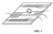
- FIG. 1illustrates one embodiment of a capacitive sensor in accordance with the invention.
- FIG. 2illustrates one sectional view of a capacitive sensor in accordance with the invention.
- FIG. 3illustrates one sectional view of a capacitive sensor in accordance with the invention.
- FIG. 4illustrates one embodiment of a capacitive sensor having at least one graphic, visible to a user, in accordance with the invention.
- FIG. 5illustrates an exploded view of one embodiment of an electronic device employing embodiments of the present invention.
- FIG. 6illustrates a sectional view of an electronic device employing embodiments of the present invention.
- FIG. 7illustrates one embodiment of a twisted-nematic display for use in an electronic device employing embodiments of the invention.
- FIG. 8illustrates one embodiment of an electronic device employing embodiments of the invention when in an OFF, low-power, sleep, or idle mode.
- FIG. 9illustrates one embodiment of an electronic device employing embodiments of the invention when active.
- FIG. 10illustrates one embodiment of a method for constructing a capacitive sensor in accordance with embodiments of the invention.
- embodiments of the present inventionrelate to a capacitive sensor for an electronic device that is configured to present selected graphics to a user.
- the graphicsmay include symbols, brand marks, logos, and other information, and are visible to a user when looking at the user interface of the electronic device.
- the electronic deviceincludes a “morphing” interface where user actuation targets are selectively hidden and revealed as the active mode of the device changes.
- a “morphing” interfacewhere user actuation targets are selectively hidden and revealed as the active mode of the device changes.
- the keypad interfaceseach comprise a plurality of user actuation targets.
- the keypad configurationsare associated with a particular mode of operation of the device.
- One embodiment of the present inventionincludes a capacitive sensor having a substrate that is configured to transmit light.
- substratesinclude at least semi-transparent plastic or glass.
- Disposed upon the substrateis a layer of capacitive sensor material that is electrically conductive and is also configured to transmit light.
- a layer of electrically conductive materialis disposed on the capacitive sensor material. As the electrically conductive material is electrically coupled to the capacitive sensor material, the electrically conductive material does not electrically interfere with the operation of the capacitive sensor.
- the electrically conductive materialhas a reflectivity that is greater than that of the capacitive sensor material, and thus reflects light back to the user. The user perceives this as visible printing on the user interface.
- the capacitive sensor 100includes a plurality of capacitive sensing devices 102 , 103 , 104 , 105 disposed along a substrate 101 .
- Each of the plurality of capacitive sensing devices 102 , 103 , 104 , 105comprises a layer of capacitor sensor material deposited on the substrate 101 .
- the substrateis configured to transmit incident light.
- the substratemay be manufactured from thin plastic film, sheet plastic, or reinforced glass.
- each of the plurality of capacitive sensing devices 102 , 103 , 104 , 105is configured, in conjunction with associated control circuitry, to detect an object in close proximity with—or touching—a user interface of the electronic device.
- the layer of capacitive sensor materialis electrically conductive, and, in one embodiment, is pellucid.
- the layer of capacitive sensor materialis arranged, as shown in FIG. 1 , as a plurality of capacitive electrodes.
- One method of forming the transparent or at least semi-transparent plurality of capacitive sensing devices 102 , 103 , 104 , 105is by printing solid indium-tin oxide (In.sub.2 O.sub.3 SnO.sub.2) (ITO) in the desired capacitor device patterns atop the substrate 101 .
- Indium tin oxideis a mixture of indium oxide and tin oxide.
- indium tin oxideis substantially transparent and conductive, and is capable of being deposited in thin layers by way of a printing process.
- Indium tin oxideis well suited for embodiments of the present invention due to its combination of electrical conduction properties and optical transparency.
- the plurality of capacitive sensing devices 102 , 103 , 104 , 105may be deposited on the substrate 101 in any of a variety of ways, including electron beam evaporation, physical vapor deposition, or other various sputter deposition techniques.
- other materialsincluding patterned conductive inks, may also used in the capacitor electrode construction.
- FIG. 2illustrated therein is a sectional view of a capacitive sensor 200 for an electronic device configured to present selected graphics to a user in accordance with embodiments of the invention.
- the layer of capacitive sensor material 201is shown as a continuous layer for illustrative purposes. In practice, the layer of capacitive sensor material 201 may be initially deposited as a continuous layer and then selectively etched, thereby forming the desired electrode patterns.
- a layer of selectively disposed electrically conductive material 202Deposited upon the layer of capacitive sensor material 201 (although it could also be deposited beneath the layer of capacitive sensor material 201 ) is a layer of selectively disposed electrically conductive material 202 .
- the layer of selectively disposed electrically conductive material 202may be selectively deposited so as to be arranged as a graphic. This graphic can be a symbol, an alphanumeric character or text, a key or user actuation target, a navigation device, a brand mark, a logo, an identifier, an artistic rendering, or other pattern.
- the layer of selectively disposed electrically conductive material 202is electrically coupled to the layer of capacitive sensor material 201 .
- the layer of selectively disposed electrically conductive material 202has a greater reflectivity than does the layer of capacitive sensor material 201 .
- the reflectivity of the layer of selectively disposed electrically conductive material 202is at least twice that of the layer of capacitive sensor material 201 . While both may be pellucid, more light passes through the layer of capacitive sensor material 201 than the layer of selectively disposed electrically conductive material 202 . Thus, more light is reflected from the layer of selectively disposed electrically conductive material 202 than from the layer of capacitive sensor material 201 .
- this layerserves as “printing” in that the user can see the graphic due to the difference in reflectivity.
- the layer of selectively disposed electrically conductive material 202has a reflectivity that the same or less than the layer of capacitive sensor material.
- both the layer of capacitive sensor material 201 and the layer of selectively disposed electrically conductive material 202are indium-tin oxide layers.
- the reflectivity of the indium-tin oxide used for the layer of selectively disposed electrically conductive material 202can be increased relative to that of the layer of capacitive sensor material 201 by altering the indium and tin concentrations. Specifically, oxygen can be removed, thereby increasing the proportions of indium and tin.
- This increase in indium and tin concentrationhas two effects: First, it reduces the characteristic impedance of the overall indium-tin oxide. Second, it makes the resulting indium-tin oxide less transparent or more reflective.
- the metallic reflective properties of the resulting indium-tin oxidebecomes more visible to a user.
- the lower resistance (i.e., more reflective) indium-tin oxideis arranged geometrically as a desired graphical design, while the standard, higher resistance (i.e., less reflective) indium-tin oxide is patterned elsewhere, the visual effect of a graphical design having a metallic finish is achieved without introducing electrical interference to the capacitive sensor 200 .
- indium-tin oxide having a characteristic impedance of around 300 Ohmsis suitable for use as the layer of capacitive sensor material 201
- indium-tin oxide having a characteristic impedance of around 100 Ohms (or less)is suitable for use as the layer of selectively disposed electrically conductive material.
- the layer of capacitive sensor material 201 and the layer of selectively disposed electrically conductive material 202may both be indium-tin oxide.
- the layer of selectively disposed electrically conductive material 202may be fashioned by selectively depositing layer upon layer of the same indium-tin oxide used as the layer of capacitive sensor material 201 . By depositing multiple layers atop each other, the thickness of the indium-tin oxide increases, causing the characteristic impedance to go down and the reflectivity to increase
- metalsuch as gold, tin, copper, nickel, or aluminum
- the layer of selectively disposed electrically conductive material 202may be used as the layer of selectively disposed electrically conductive material 202 .
- the layer of capacitive sensor material 201is indium-tin oxide
- the layer of metalwill have a greater reflectivity as the layer of metal will generally be opaque.
- the layer of metal, serving as a metallic conductorwill generally have an impedance of well less than 100 Ohms. This is generally more conductive than standard (highly transparent) indium-tin oxide.
- the response time associated with the capacitive sensor 200will decrease, corresponding to a reduced RC time constant, thereby resulting in a decrease in the time needed to charge or discharge the associated capacitance through the associated resistance.
- the layer of selectively disposed electrically conductive material 202is shown in FIG. 2 as being deposited on the same side of the substrate 101 as the layer of capacitive sensor material 201 , it will be clear to those of ordinary skill in the art having the benefit of this disclosure that the invention is not so limited.
- the layer of selectively disposed electrically conductive material 202could equally be disposed on the opposite side of the substrate 101 , with the electrical coupling to the layer of capacitive sensor material 201 being achieved by vias through the substrate 101 or by connectors passing about the sides of the substrate 101 .
- the layer of selectively disposed electrically conductive material 202may be patterned in the shape of the desired graphical design on either side of the layer of capacitive sensor material 201 . As the layer of selectively disposed electrically conductive material 202 is in electrical contact with the layer of capacitive sensor material 201 , the layers work together to transmit the electric field used for capacitive sensing, while producing a visible graphical design.
- FIG. 3illustrated therein is an alternate embodiment of a capacitive sensor 300 in accordance with embodiments of the invention.
- the layer of selectively disposed electrically conductive material ( 202 ) in FIG. 2was shown as being disposed atop the layer of capacitive sensor material ( 201 )
- the layer of selectively disposed electrically conductive material 302is interspersed with the layer of capacitive sensor material 301 . Such interspersion may be accomplished either by selective printing or by masking.
- the capacitive sensor 200comprises at least two types of sensor material—a first material having a lower reflectivity and a second material having a higher reflectivity.
- the second materialmay be a thicker layer of the first material. The two materials are electrically coupled together.
- the first materialdeposited as the layer of capacitive sensor material 201 , is arranged as a plurality of capacitive electrodes.
- the second materialapplied as the selectively disposed electrically conductive material 202 , is arranged as at least one graphic 401 that will be visible through a transparent cover layer of an electronic device.
- the graphic 401shown illustratively as the letter “A” in FIG. 4 , may be a device model, brand mark, or other identifier.
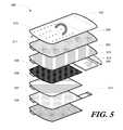
- FIG. 5illustrated therein is an exploded view of a dynamic user interface 500 for a portable electronic device that employs a capacitive sensor 200 in accordance with one embodiment of the invention.
- the user interface 500is made from several layers, each layer implementing a different function. While several layers are shown, it will be clear to those of ordinary skill in the art having the benefit of this disclosure that each and every layer may not be required for a specific application.
- the structure of FIG. 5is exemplary only.
- the user interface 500includes the following components: a cover layer 502 ; a capacitive sensor 200 ; an optical shutter assembly 504 ; an electroluminescent device 505 , a resistive switch layer 506 ; a substrate layer 507 ; and a tactile feedback layer 508 . Additionally, a high-resolution display 509 and filler materials 510 may be included to complete the assembly. While the layers are shown individually, it will be clear to those of ordinary skill in the art having the benefit of this disclosure that some of the various layers may be combined together. For instance, the cover layer 502 and capacitive sensor 200 may be integrated together to form a single layer. Similarly, the tactile feedback layer 508 may be integrated into the cover layer 502 , and so forth.
- a thin film sheetserves as a unitary fascia member for the electronic device.
- a “fascia”is a covering or housing, which may or may not be detachable, for an electronic device like a mobile telephone. While the drawings herein employ a mobile telephone as an exemplary electronic device for discussion, it will be clear to those of ordinary skill in the art having the benefit of this disclosure that the invention is not so limited.
- the fascia of the present inventioncould be used for any electronic device having a display and a keypad.
- the cover layer 502in one exemplary embodiment, is a thin, flexible membrane. Suitable materials for manufacturing the thin, flexible membrane include clear or translucent plastic film, such as 0.4 millimeter, clear polycarbonate film. In another embodiment, the cover layer 502 is manufactured from a thin sheet of reinforced glass. The cover layer, being continuous and without holes or other apertures or perforations, is well suited to serve as a continuous fascia for the electronic device, keeping dust, debris and liquids from invading the device.
- Printingmay be disposed on the rear face 511 of the cover layer 502 . Even where the capacitive sensor 200 and its non-electrically interfering printing in accordance with the invention is used, some peripheral selective printing on the cover layer may still be desirable. For instance, printing may be desired around the perimeter of the cover layer 502 to cover electrical traces connecting the various layers. Such peripheral printing generally does not significantly affect the performance of the capacitive sensor 200 .
- Non-conductive printingmay be desired on the front face 513 for various reasons as well.
- a subtle textural printing or overlay printingmay be desirable to provide a translucent matte finish atop the electronic device.
- mechanical finishing techniquesmay apply such a matte finish.
- Such a finishis useful to prevent cosmetic blemishing from sharp objects or fingerprints.
- the cover layer 502may also include an ultra-violet barrier. Such a barrier is useful both in improving the visibility of the high-resolution display 509 and in protecting internal components of the electronic device.
- the capacitive sensor 200may be any of the capacitive sensor structures described herein.
- the capacitive sensor 200which is formed by depositing small capacitive plate electrodes on a substrate, is configured to detect the presence of an object, such as a user's finger, near to or touching the user interface 500 .
- Control circuitryoperating as a detector, detects a change in the capacitance of a particular plate combination on the capacitive sensor 200 .
- the capacitive sensor 200may be used in a general mode, for instance to detect the general proximate position of an object relative to the device.
- the capacitive sensor 200may also be used in a specific mode, where a particular capacitor electrode pair may be detected to detect the location of an object along length and width of the front surface of the electronic device. In this mode, the capacitive sensor 200 may be used to detect the proximate position of an object, such as a user's finger, relative to any of the actuation targets presented.
- this layerincludes a segmented electro-optical device configured as an optical shutter.
- a “segmented” electro-optical display deviceis used herein to mean a display device with less granularity than the high-resolution display 509 .
- a “high-resolution display”refers to a device that can present text and images to a user by altering a large number of pixels which, when viewed collectively by a user, form the presented text or image.
- the high-resolution displayis a display suitable for the presentation of text, information, and graphics on a mobile device with sufficient granularity as to be easily switched between graphics or text.
- the high-resolution displaywould be one suitable for presenting an image in the Joint Photographics Expert Group (JPG) format to the user.
- JPGJoint Photographics Expert Group
- Such displaysgenerally are configured to turn on and off individual pixels by way of a display driver for the presentation of high-resolution information. Examples include a 256 pixel by 128 pixel reflective or backlit LCD.
- Such display devicesare manufactured by Samsung and Sony.
- a segmented displayis a display device with less granularity than the high-resolution device.
- the segmented display deviceis capable of actuating a predefined segment or segments to present a predetermined text or symbol graphic to a user, but does not have sufficient granularity to easily transition from, for example, text to graphics.
- the segmented display of the optical shutter assembly 504uses electrodes placed atop and beneath the optical shutter assembly 504 to open and close “windows”, thereby transforming the window from a first, opaque state to a second, translucent state.
- the optical shutter assembly 504is “segmented” because individual windows, or shutters, may be controlled. Further, by configuring the electrodes on at least one side of the optical shutter assembly 504 , each shutter can be configured as the alphanumeric indicia, which may include numbers, letters, or symbols forming images representative of a plurality of actuatable keys.
- the optical shutter assembly 504is configured to present any of a plurality of keypad configurations to a user.
- Each keypad configurationin one embodiment, corresponds to a particular mode of operation of the electronic device. For example, a music player mode may correspond to a first keypad configuration, while a phone mode may correspond to an alternate configuration.
- the optical shutter assembly 504presents each of the plurality of keypad configurations by transitioning segments of the optical shutter assembly 504 from opaque states to translucent states. When translucent, light can pass through each shutter. When opaque, light is absorbed. The result is a reveal and concealment of each individual key. Each key forms an actuation target that can be selected by the user.
- An electroluminescent device 505may be included to provide a backlighting function to the shutters of the optical shutter assembly 504 .
- electroluminescentrefers to any device capable of producing luminescence electrically, including light emitting diodes, and equivalent devices. Such a function is useful in improving the visibility of the keypad region in low-light conditions.
- the electroluminescent device 505includes a layer of backlight material sandwiched between a transparent substrate bearing transparent electrodes on the top and bottom. The electrodes, which may be segmented and patterned to correspond with the shutters of the optical shutter assembly 504 . One electrode is an actuation electrode, while another electrode is a ground electrode. Where the electrodes are segmented, the actuation electrode is generally patterned.
- a reflector, integrated into the back of the electroluminescent device 505allows incident light to be reflected back through the display, even when the electroluminescent elements are active.
- the high-resolution display 509which may have its own lighting system and may also include a polarizing layer 515 configured to polarize light along an axis of polarization, may be placed adjacent to the electroluminescent device 505 . Further, filler material 510 may be included to complete the assembly.
- the resistive switch layer 506includes a force switch array configured to detect contact with any of one of the shutters dynamic keypad region or any of the plurality of actuation targets.
- An “array” as used hereinrefers to a set of at least one switch. For instance, where the cover layer 502 is manufactured from glass, one switch may be all that is necessary. However, when the cover layer 502 is manufactured from thin film plastic, multiple switches may be employed.
- the array of resistive switchesfunctions as a force-sensing layer, in that when contact is made with the front surface, changes in impedance of any of the switches may be detected.
- the array of switchesmay be any of resistance sensing switches, membrane switches, force-sensing switches such as piezoelectric switches, or other equivalent types of technology.
- the cover layer 502When the cover layer 502 is made from thin plastic film, an array of switches may be included on the resistive switch layer to detect the proximate location of a finger actuating one of the keys. Experimental results have shown that a deflection of as little as 40 um along the cover layer is sufficient to actuate one of the resistive switches.
- the capacitive sensor 200When the cover layer 502 is made from glass, the capacitive sensor 200 may be used to detect the proximate location, while one or more switches on the resistive switch layer 506 may be used to detect actuation of the rigid cover layer 502 . By employing control circuitry to combine this data, the exact shutter, region, and/or target actuated may be properly detected.
- a substrate layer 507is provided to carry the various conduits to control circuits and drivers for the layers of the display.
- the substrate layer 507which may be either a rigid layer such as FR4 printed wiring board or a flexible layer such as copper traces printed on a flexible material such as Kapton®, includes electrical connections to components, integrated circuits, processors, and associated circuitry to control the operation of the display.
- the substrate layer 507includes a connector 514 for coupling to the detector and other electrical components within the electronic device.
- a modicum of deflectionis all that is required to actuate one of the keys presented by the optical shutter assembly 504 .
- the cover layer 402is manufactured from thin film plastic
- a minor deflection of the plasticwill actuate a switch on the resistive switch layer 506 .
- the cover layer 502is manufactured from glass
- a minor deflection of the entire cover layer 502will actuate a switch on the resistive switch layer 506 .
- This deflectionis on the order of tens of micrometers. As such, a user may not perceive any deflection at all when pressing each key.
- the tactile feedback layer 508may include a transducer configured to provide a sensory feedback when a switch on the resistive switch layer detects actuation of a key.
- the transduceris a piezoelectric transducer configured to apply a mechanical “pop” to the user interface 500 that is strong enough to be detected by the user.
- the tactile feedback layerprovides sensory feedback to the user, thereby making the smooth, substantially planar user interface 500 react more like a conventional keypad without the need of individual popple-enabled keys protruding through the keypad.
- FIG. 6illustrated therein is a side view of the user interface. Each layer may be seen from the side in a cut-away view. Again, it will be clear to those of ordinary skill in the art having the benefit of this disclosure that the invention is not limited to the specific structure shown in FIG. 6 . Some layers, as noted above, are optional and may not be included in certain applications.
- the layersmay be coupled together in any of a variety of ways.
- One exemplary embodiment of a coupling mechanismis by using a thin layer of clear (transparent), non-conductive adhesive.
- the cover layer 502 , the capacitive sensor 200 , and the optical shutter assembly 504may each be mechanically coupled together with non-conductive, translucent adhesive. This coupling keeps the overall assembly properly aligned within the device.
- the cover layer 502which may be either a thin film plastic or glass layer. Where glass is used, reinforced glass is often preferred to provide additional reliability to the user interface ( 500 ).
- the glassmay be reinforced by a strengthening process, such as a chemical or heat treatment process.
- the cover layermay include printing disposed thereon.
- the capacitive sensor 200includes both the capacitive sensor material 201 and substrate layer 101 .
- the substrate layer 101which may be either rigid, or soft (for instance a silicone layer), carries the electrode plates that form the capacitive sensors.
- the electrodesmay be used in a singular configuration, or in pairs. Further alternate electrode pairs, including electrode groupings of two, four, or six electrodes, may be used to form the capacitive sensors.
- the at least one graphic ( 401 )is also included.
- the segmented electro-optical device of the optical shutter assembly 504is manufactured using a twisted nematic liquid crystal display material.
- Other materialsincluding polymer-dispersed liquid crystal material, super twisted nematic liquid crystal material, ferro-electric liquid crystal material, electrically-controlled birefringent material, optically-compensated bend mode material, guest-host materials, and other types of light modulating may equally be used.
- the optical shutter assembly 504includes twisted nematic liquid crystal display material 603 that is sandwiched between two electrodes 604 , 605 and two substrates 606 , 607 .
- the electrodes 604 , 605 and substrates 606 , 607are preferably transparent, such that light can pass freely through each.
- the substrates 606 , 607may be manufactured from either plastic or glass.
- the upper electrode 604is constructed, in one embodiment using indium-tin oxide affixed to substrate 606 .
- the lower electrode 605is constructed using a patterned indium-tin oxide layer affixed to the lower substrate 607 .
- the patternsare those of alphanumeric keys or symbols representing keys or user actuation targets of the device.
- both electrodes 604 , 605can be patterned; however, user visibility may be affected where both electrodes 604 , 605 are patterned.
- the patterned electrode(s) 605by way of patterned electrical traces, is connected to a control circuit 608 , which may also connect to the capacitive sensor 200 .
- the control circuit 608applies a field to the patterned electrode(s) 305 , while the other electrode 304 acts as a ground.
- the electric field appliedalters the light transmission properties of the twisted nematic liquid crystal display material 603 .
- the electric fieldcan cause sections under each of the patterned electrodes 605 to transition from a first state to a second state.
- the first statemay be opaque, while the second state is translucent.
- the patterns of the patterned electrodes 605define the images of each shutter in the optical shutter.
- a shuttercan be patterned as a “9 key” for a phone by patterning one electrode as a box (i.e. the boundary of the key), and another electrode as the “9 wxyz” characters.
- the shuttersthus act as “windows” that can be open or closed, to reveal or hide images.
- the optical shutter assembly 504also includes multiple polarizing layers disposed atop and beneath the optical shutter. These polarizing layers polarize light along a polarization axis and provide a predetermined color to the overall display assembly.
- a liquid crystal displaymay be disposed between the capacitive sensor 200 and the optical shutter assembly 504 .
- the liquid crystal displayis used to present graphics through the capacitive sensor 200 to the user.
- the electroluminescent device 505includes a layer of electroluminescent material 609 sandwiched between a transparent substrate 610 bearing a single, or patterned, indium tin oxide electrode(s) 611 and a ground electrode 612 .
- the patterned electrode 611 of the electroluminescent device 505is aligned with the various shutters of the optical shutter assembly 504 .
- the ground electrode 612may comprise a solid conductive ink layer printed on the bottom surface of the electroluminescent material 609 . This solid conductive ink layer may have reflective properties.
- the electroluminescent device 505may have a reflective layer integrated beneath the ground electrode 612 .
- the ground electrode 612may be patterned and may be borne on a reflective substrate if desired.
- One electrode layer 601is connected to control circuit 608 .
- the high-resolution display 509is disposed at least partially under the optical shutter assembly 254 .
- the optical shutter assembly 504passes across the high-resolution display 509 , thereby covering at least a portion of the high-resolution display 509 .
- the high-resolution display 509is completely hidden. This action gives the overall device a “blank” face when the electronic device is OFF.
- Beneath the electroluminescent device 505are the resistive switch layer 506 , the substrate layer 507 , and the tactile feedback layer 508 with its transducer 615 .
- FIG. 7illustrated therein is an exploded view of an optical shutter assembly 504 .
- the optical shutter assembly 504in accordance with the illustrated exemplary embodiment, is referred to as “twisted” because it contains liquid crystal elements that twist and untwist in differing amounts to allow light to pass through.
- a first polarizer 701is disposed on one side of the device to polarize incident light.
- a substrate 606having indium tin oxide electrodes (as previously discussed) printed in varying shapes is disposed adjacent to the polarizer.
- the electrodesmay be disposed in shapes that correspond to the alphanumeric keys or symbols associated with the keys of the electronic device.
- Twisted nematic liquid crystal display material 603is then next, followed by another substrate 607 configured with ground electrodes.
- a horizontal filter 702then is used to permit and block light.
- a reflective or transflective surface 703may optionally be used to reflect light back (in a reflective mode), or to transmit light in a transflective mode.
- the deviceWhen no voltage is applied to the electrodes, the device is in a first state. When voltage is applied the liquid crystal material twists—in incremental amounts up to 90 degrees—thereby changing the luminous polarization.
- This liquid crystalthus acts as a controllable polarizer, controlled by electrical signals applied to the electrodes. Adjustment of the voltage being applied to the electrodes permits varying levels grey, as well as transparent states or opaque states to be created. Embodiments of the present invention use this device as a low-resolution display to reveal and hide keys.
- FIG. 8illustrated therein is an electronic device 800 having a user interface 801 configured to receive touch input in accordance with embodiments of the invention.
- the electronic device 800 of FIG. 2shown illustratively as a radiotelephone, is in the OFF mode.
- the view of FIG. 8may also arise when the electronic device 800 is in a low power state, a sleep state, or an idle mode.
- the optical shutter assembly ( 504 )covers both the keypad region and the high resolution display
- the user interface 801 of the electronic device 800will be blank when the device is in this state. This occurs because each of the shutters is closed (i.e. in the opaque state), thereby prohibiting visibility of either the high-resolution display or any of the plurality of keypad configurations. Small demarcations may be present on the cover layer of the device to orient the user to the keypad region.
- FIG. 9illustrated therein is the electronic device 800 from FIG. 8 having changed from the OFF state (or alternatively a low power state) to an ON state.
- the electronic device 800may be converted from the OFF or low power mode to an ON mode in one of a variety of ways.
- a first methodis for a user to actuate the capacitive sensor.
- a second methodis from an external event or a device event.
- the electronic device 800opens at least one display segment 901 , thereby transitioning that segment 901 to the translucent state.
- One configuration of the plurality of keypad configurations 902 , or the high-resolution display 509 , or both,then becomes visible to the user.
- at least a curved scroll device 903is presented on the user interface surface.
- a layer of semi-transparent, electrically conductive materialsuch as indium-tin oxide, is deposited on a substrate.
- a layer of electrically conductive materialis deposited selectively on the semi-transparent, electrically conductive material as visible graphic indicia.
- the layer of electrically conductive materialmay be any of a thicker layer of indium-tin oxide, a layer of indium-tin oxide with a different doping, a layer of metal such as gold or aluminum, or other equivalent material.
- the layer of electrically coupled materialis deposited such that it is electrically coupled to the layer of semi-transparent, electrically conductive material. Additionally, the layer of electrically conductive material has a greater reflectivity than does the layer of semitransparent, electrically conductive material.
- both the layer of semi-transparent, electrically conductive material and the layer of electrically conductive materialmay be etched, thereby yielding or forming a predetermined electrode pattern. While both the layer of semi-transparent, electrically conductive material and the layer of electrically conductive material will be etched, the visible graphic indicia will still be legible so long as the spacing between the electrodes is sufficiently small.
Landscapes
- Engineering & Computer Science (AREA)
- General Engineering & Computer Science (AREA)
- Theoretical Computer Science (AREA)
- Human Computer Interaction (AREA)
- Physics & Mathematics (AREA)
- General Physics & Mathematics (AREA)
- Position Input By Displaying (AREA)
Abstract
Description
Claims (20)
Priority Applications (2)
| Application Number | Priority Date | Filing Date | Title |
|---|---|---|---|
| US11/838,061US8077154B2 (en) | 2007-08-13 | 2007-08-13 | Electrically non-interfering printing for electronic devices having capacitive touch sensors |
| PCT/US2008/071677WO2009023440A1 (en) | 2007-08-13 | 2008-07-31 | Electrically non-interfering printing for electronic devices having capacitive touch sensors |
Applications Claiming Priority (1)
| Application Number | Priority Date | Filing Date | Title |
|---|---|---|---|
| US11/838,061US8077154B2 (en) | 2007-08-13 | 2007-08-13 | Electrically non-interfering printing for electronic devices having capacitive touch sensors |
Publications (2)
| Publication Number | Publication Date |
|---|---|
| US20090046072A1 US20090046072A1 (en) | 2009-02-19 |
| US8077154B2true US8077154B2 (en) | 2011-12-13 |
Family
ID=40351052
Family Applications (1)
| Application Number | Title | Priority Date | Filing Date |
|---|---|---|---|
| US11/838,061Active2030-05-09US8077154B2 (en) | 2007-08-13 | 2007-08-13 | Electrically non-interfering printing for electronic devices having capacitive touch sensors |
Country Status (2)
| Country | Link |
|---|---|
| US (1) | US8077154B2 (en) |
| WO (1) | WO2009023440A1 (en) |
Cited By (81)
| Publication number | Priority date | Publication date | Assignee | Title |
|---|---|---|---|---|
| US20110260741A1 (en)* | 2010-04-27 | 2011-10-27 | 3M Innovative Properties Company | Integrated passive circuit elements for sensing devices |
| US8456438B2 (en) | 2008-01-04 | 2013-06-04 | Tactus Technology, Inc. | User interface system |
| US8547339B2 (en) | 2008-01-04 | 2013-10-01 | Tactus Technology, Inc. | System and methods for raised touch screens |
| US8553005B2 (en) | 2008-01-04 | 2013-10-08 | Tactus Technology, Inc. | User interface system |
| US8570295B2 (en) | 2008-01-04 | 2013-10-29 | Tactus Technology, Inc. | User interface system |
| US8587541B2 (en) | 2010-04-19 | 2013-11-19 | Tactus Technology, Inc. | Method for actuating a tactile interface layer |
| US8587548B2 (en) | 2009-07-03 | 2013-11-19 | Tactus Technology, Inc. | Method for adjusting the user interface of a device |
| US8619035B2 (en) | 2010-02-10 | 2013-12-31 | Tactus Technology, Inc. | Method for assisting user input to a device |
| US8704790B2 (en) | 2010-10-20 | 2014-04-22 | Tactus Technology, Inc. | User interface system |
| US8796575B2 (en) | 2012-10-31 | 2014-08-05 | Ford Global Technologies, Llc | Proximity switch assembly having ground layer |
| US8878438B2 (en) | 2011-11-04 | 2014-11-04 | Ford Global Technologies, Llc | Lamp and proximity switch assembly and method |
| US8922340B2 (en) | 2012-09-11 | 2014-12-30 | Ford Global Technologies, Llc | Proximity switch based door latch release |
| US8922503B2 (en) | 2008-01-04 | 2014-12-30 | Tactus Technology, Inc. | User interface system |
| US8922510B2 (en) | 2008-01-04 | 2014-12-30 | Tactus Technology, Inc. | User interface system |
| US8922502B2 (en) | 2008-01-04 | 2014-12-30 | Tactus Technology, Inc. | User interface system |
| US8928621B2 (en) | 2008-01-04 | 2015-01-06 | Tactus Technology, Inc. | User interface system and method |
| US8928336B2 (en) | 2011-06-09 | 2015-01-06 | Ford Global Technologies, Llc | Proximity switch having sensitivity control and method therefor |
| US8933708B2 (en) | 2012-04-11 | 2015-01-13 | Ford Global Technologies, Llc | Proximity switch assembly and activation method with exploration mode |
| US8947383B2 (en) | 2008-01-04 | 2015-02-03 | Tactus Technology, Inc. | User interface system and method |
| US8975903B2 (en) | 2011-06-09 | 2015-03-10 | Ford Global Technologies, Llc | Proximity switch having learned sensitivity and method therefor |
| US8981602B2 (en) | 2012-05-29 | 2015-03-17 | Ford Global Technologies, Llc | Proximity switch assembly having non-switch contact and method |
| US8994228B2 (en) | 2011-11-03 | 2015-03-31 | Ford Global Technologies, Llc | Proximity switch having wrong touch feedback |
| US9013417B2 (en) | 2008-01-04 | 2015-04-21 | Tactus Technology, Inc. | User interface system |
| US9052790B2 (en) | 2008-01-04 | 2015-06-09 | Tactus Technology, Inc. | User interface and methods |
| US9065447B2 (en) | 2012-04-11 | 2015-06-23 | Ford Global Technologies, Llc | Proximity switch assembly and method having adaptive time delay |
| US9063627B2 (en) | 2008-01-04 | 2015-06-23 | Tactus Technology, Inc. | User interface and methods |
| US9075525B2 (en) | 2008-01-04 | 2015-07-07 | Tactus Technology, Inc. | User interface system |
| US9116617B2 (en) | 2009-07-03 | 2015-08-25 | Tactus Technology, Inc. | User interface enhancement system |
| US9136840B2 (en) | 2012-05-17 | 2015-09-15 | Ford Global Technologies, Llc | Proximity switch assembly having dynamic tuned threshold |
| US9143126B2 (en) | 2011-09-22 | 2015-09-22 | Ford Global Technologies, Llc | Proximity switch having lockout control for controlling movable panel |
| US9184745B2 (en) | 2012-04-11 | 2015-11-10 | Ford Global Technologies, Llc | Proximity switch assembly and method of sensing user input based on signal rate of change |
| US9197206B2 (en) | 2012-04-11 | 2015-11-24 | Ford Global Technologies, Llc | Proximity switch having differential contact surface |
| US9219472B2 (en) | 2012-04-11 | 2015-12-22 | Ford Global Technologies, Llc | Proximity switch assembly and activation method using rate monitoring |
| US9239623B2 (en) | 2010-01-05 | 2016-01-19 | Tactus Technology, Inc. | Dynamic tactile interface |
| US9250804B2 (en) | 2013-02-05 | 2016-02-02 | Freescale Semiconductor,Inc. | Electronic device for detecting erronous key selection entry |
| US9274612B2 (en) | 2008-01-04 | 2016-03-01 | Tactus Technology, Inc. | User interface system |
| US9280224B2 (en) | 2012-09-24 | 2016-03-08 | Tactus Technology, Inc. | Dynamic tactile interface and methods |
| US9287864B2 (en) | 2012-04-11 | 2016-03-15 | Ford Global Technologies, Llc | Proximity switch assembly and calibration method therefor |
| US9298261B2 (en) | 2008-01-04 | 2016-03-29 | Tactus Technology, Inc. | Method for actuating a tactile interface layer |
| US9311204B2 (en) | 2013-03-13 | 2016-04-12 | Ford Global Technologies, Llc | Proximity interface development system having replicator and method |
| US9337832B2 (en) | 2012-06-06 | 2016-05-10 | Ford Global Technologies, Llc | Proximity switch and method of adjusting sensitivity therefor |
| US9367132B2 (en) | 2008-01-04 | 2016-06-14 | Tactus Technology, Inc. | User interface system |
| US9372565B2 (en) | 2008-01-04 | 2016-06-21 | Tactus Technology, Inc. | Dynamic tactile interface |
| US9405417B2 (en) | 2012-09-24 | 2016-08-02 | Tactus Technology, Inc. | Dynamic tactile interface and methods |
| US9423875B2 (en) | 2008-01-04 | 2016-08-23 | Tactus Technology, Inc. | Dynamic tactile interface with exhibiting optical dispersion characteristics |
| US9520875B2 (en) | 2012-04-11 | 2016-12-13 | Ford Global Technologies, Llc | Pliable proximity switch assembly and activation method |
| US9531379B2 (en) | 2012-04-11 | 2016-12-27 | Ford Global Technologies, Llc | Proximity switch assembly having groove between adjacent proximity sensors |
| US9548733B2 (en) | 2015-05-20 | 2017-01-17 | Ford Global Technologies, Llc | Proximity sensor assembly having interleaved electrode configuration |
| US9552065B2 (en) | 2008-01-04 | 2017-01-24 | Tactus Technology, Inc. | Dynamic tactile interface |
| US9559688B2 (en) | 2012-04-11 | 2017-01-31 | Ford Global Technologies, Llc | Proximity switch assembly having pliable surface and depression |
| US9557915B2 (en) | 2008-01-04 | 2017-01-31 | Tactus Technology, Inc. | Dynamic tactile interface |
| US9557813B2 (en) | 2013-06-28 | 2017-01-31 | Tactus Technology, Inc. | Method for reducing perceived optical distortion |
| US9568527B2 (en) | 2012-04-11 | 2017-02-14 | Ford Global Technologies, Llc | Proximity switch assembly and activation method having virtual button mode |
| US9588684B2 (en) | 2009-01-05 | 2017-03-07 | Tactus Technology, Inc. | Tactile interface for a computing device |
| US9588683B2 (en) | 2008-01-04 | 2017-03-07 | Tactus Technology, Inc. | Dynamic tactile interface |
| US9612659B2 (en) | 2008-01-04 | 2017-04-04 | Tactus Technology, Inc. | User interface system |
| US9641172B2 (en) | 2012-06-27 | 2017-05-02 | Ford Global Technologies, Llc | Proximity switch assembly having varying size electrode fingers |
| US9654103B2 (en) | 2015-03-18 | 2017-05-16 | Ford Global Technologies, Llc | Proximity switch assembly having haptic feedback and method |
| US9660644B2 (en) | 2012-04-11 | 2017-05-23 | Ford Global Technologies, Llc | Proximity switch assembly and activation method |
| US9720501B2 (en) | 2008-01-04 | 2017-08-01 | Tactus Technology, Inc. | Dynamic tactile interface |
| US9760172B2 (en) | 2008-01-04 | 2017-09-12 | Tactus Technology, Inc. | Dynamic tactile interface |
| US9831870B2 (en) | 2012-04-11 | 2017-11-28 | Ford Global Technologies, Llc | Proximity switch assembly and method of tuning same |
| US9874965B2 (en) | 2015-09-11 | 2018-01-23 | Apple Inc. | Transparent strain sensors in an electronic device |
| US9886118B2 (en) | 2015-09-30 | 2018-02-06 | Apple Inc. | Transparent force sensitive structures in an electronic device |
| US9944237B2 (en) | 2012-04-11 | 2018-04-17 | Ford Global Technologies, Llc | Proximity switch assembly with signal drift rejection and method |
| US9952703B2 (en) | 2013-03-15 | 2018-04-24 | Apple Inc. | Force sensing of inputs through strain analysis |
| US10006820B2 (en) | 2016-03-08 | 2018-06-26 | Apple Inc. | Magnetic interference avoidance in resistive sensors |
| US10004286B2 (en) | 2011-08-08 | 2018-06-26 | Ford Global Technologies, Llc | Glove having conductive ink and method of interacting with proximity sensor |
| US10038443B2 (en) | 2014-10-20 | 2018-07-31 | Ford Global Technologies, Llc | Directional proximity switch assembly |
| US10055048B2 (en) | 2015-07-31 | 2018-08-21 | Apple Inc. | Noise adaptive force touch |
| US10088937B2 (en) | 2012-05-03 | 2018-10-02 | Apple Inc. | Touch input device including a moment compensated bending sensor for load measurement on platform supported by bending beams |
| US10112556B2 (en) | 2011-11-03 | 2018-10-30 | Ford Global Technologies, Llc | Proximity switch having wrong touch adaptive learning and method |
| US10120478B2 (en) | 2013-10-28 | 2018-11-06 | Apple Inc. | Piezo based force sensing |
| US10133418B2 (en) | 2016-09-07 | 2018-11-20 | Apple Inc. | Force sensing in an electronic device using a single layer of strain-sensitive structures |
| US10139294B2 (en) | 2015-07-21 | 2018-11-27 | Apple Inc. | Strain sensors in an electronic device |
| US10209830B2 (en) | 2016-03-31 | 2019-02-19 | Apple Inc. | Electronic device having direction-dependent strain elements |
| US10309846B2 (en) | 2017-07-24 | 2019-06-04 | Apple Inc. | Magnetic field cancellation for strain sensors |
| US10423265B2 (en) | 2014-01-13 | 2019-09-24 | Apple Inc. | Temperature compensating force sensor |
| US10444091B2 (en) | 2017-04-11 | 2019-10-15 | Apple Inc. | Row column architecture for strain sensing |
| EP3640771A2 (en) | 2018-10-15 | 2020-04-22 | Tangi0 Limited | Sensor device and method |
| US10782818B2 (en) | 2018-08-29 | 2020-09-22 | Apple Inc. | Load cell array for detection of force input to an electronic device enclosure |
Families Citing this family (29)
| Publication number | Priority date | Publication date | Assignee | Title |
|---|---|---|---|---|
| EP2193693A4 (en)* | 2007-09-17 | 2014-01-01 | Magna Int Inc | KEYBOARD WITHOUT KEYS AND WITHOUT INTEGRATED PRESSURE Ä BACKLIGHT LIGHT EMITTING |
| US8982055B2 (en)* | 2008-01-15 | 2015-03-17 | Sony Corporation | Wireless mobile communication terminals and methods for forming the same |
| US8059232B2 (en)* | 2008-02-08 | 2011-11-15 | Motorola Mobility, Inc. | Electronic device and LC shutter for polarization-sensitive switching between transparent and diffusive states |
| US7864270B2 (en)* | 2008-02-08 | 2011-01-04 | Motorola, Inc. | Electronic device and LC shutter with diffusive reflective polarizer |
| US7755260B2 (en)* | 2008-03-10 | 2010-07-13 | Palo Alto Research Center Incorporated | Nickel structures and methods for manufacturing the same by removal of an underlying material |
| US8023261B2 (en) | 2008-09-05 | 2011-09-20 | Apple Inc. | Electronic device assembly |
| KR101030388B1 (en)* | 2009-02-27 | 2011-04-20 | 삼성전자주식회사 | Keypad assembly using optical shutter and light guide plate and portable terminal having same |
| US8731618B2 (en) | 2009-04-23 | 2014-05-20 | Apple Inc. | Portable electronic device |
| US8627220B2 (en)* | 2009-10-01 | 2014-01-07 | Blackberry Limited | Apparatus and method for invoking a function based on a gesture input |
| US8324510B2 (en)* | 2009-10-16 | 2012-12-04 | Palo Alto Research Center Incorporated | Out of plane integral conductive arms and methods for manufacturing the same |
| KR20110061422A (en)* | 2009-12-01 | 2011-06-09 | 엘지이노텍 주식회사 | Capacitive touch panel |
| US8797721B2 (en) | 2010-02-02 | 2014-08-05 | Apple Inc. | Portable electronic device housing with outer glass surfaces |
| KR20120030832A (en)* | 2010-09-20 | 2012-03-29 | 삼성전기주식회사 | Touch screen and method of manufacturing the same |
| KR20120038823A (en)* | 2010-10-14 | 2012-04-24 | 삼성전기주식회사 | Touch screen |
| KR101739797B1 (en)* | 2010-10-27 | 2017-05-26 | 삼성디스플레이 주식회사 | Touch Screen Panel |
| US9235240B2 (en) | 2010-11-11 | 2016-01-12 | Apple Inc. | Insert molding around glass members for portable electronic devices |
| US9182789B2 (en) | 2011-03-01 | 2015-11-10 | Apple Inc. | Transparent electronic device components with opaque edge coverings |
| US9727176B2 (en) | 2011-06-21 | 2017-08-08 | Synaptics Incorporated | Capacitive sensor pattern |
| KR101330757B1 (en)* | 2011-07-28 | 2013-11-18 | 엘지이노텍 주식회사 | Touch Window and LCD using the same |
| WO2014098946A1 (en)* | 2012-12-17 | 2014-06-26 | Changello Enterprise Llc | Force detection in touch devices using piezoelectric sensors |
| CN104956244B (en)* | 2013-02-01 | 2017-07-21 | 株式会社村田制作所 | Display panel with compression sensor and the electronic equipment with pressing input function |
| US9871898B2 (en) | 2013-05-08 | 2018-01-16 | Apple Inc. | Ceramic cover for electronic device housing |
| US20140338191A1 (en)* | 2013-05-15 | 2014-11-20 | Uni-Pixel Displays, Inc. | Method of manufacturing an integrated touch sensor with decorative color graphics |
| EP3007041B1 (en)* | 2013-05-27 | 2022-09-07 | Murata Manufacturing Co., Ltd. | Display panel with pressing sensor, and electronic device with pressing input function |
| US20160225299A1 (en)* | 2013-09-30 | 2016-08-04 | 3M Innovative Properties Company | Apparatus for obscuring a sensing element proximate a printed graphic |
| KR102175821B1 (en)* | 2013-11-07 | 2020-11-09 | 삼성디스플레이 주식회사 | Touch location sensing pannel having an image |
| JP6447735B2 (en)* | 2015-08-07 | 2019-01-09 | 株式会社村田製作所 | Display device |
| WO2017115010A1 (en)* | 2015-12-29 | 2017-07-06 | Teknologian Tutkimuskeskus Vtt Oy | Acoustic transducing apparatus and method |
| US12131693B2 (en)* | 2019-04-09 | 2024-10-29 | Motorola Mobility Llc | Electronic device with optically pellucid electrical conductor and systems and methods for compensating for the same |
Citations (115)
| Publication number | Priority date | Publication date | Assignee | Title |
|---|---|---|---|---|
| US3915548A (en) | 1973-04-30 | 1975-10-28 | Hughes Aircraft Co | Holographic lens and liquid crystal image source for head-up display |
| US4017848A (en) | 1975-05-19 | 1977-04-12 | Rockwell International Corporation | Transparent keyboard switch and array |
| US4078257A (en) | 1976-08-23 | 1978-03-07 | Hewlett-Packard Company | Calculator apparatus with electronically alterable key symbols |
| US4422721A (en) | 1982-08-09 | 1983-12-27 | Optical Coating Laboratory, Inc. | Optical article having a conductive anti-reflection coating |
| US4462924A (en) | 1978-09-13 | 1984-07-31 | The Secretary Of State In Her Britannic Majesty's Government Of The United Kingdom Of Great Britain And Northern Ireland | Liquid crystal materials and devices |
| US4500173A (en) | 1983-05-02 | 1985-02-19 | Timex Corporation | Electroluminescent lamp for liquid crystal display |
| US4545648A (en) | 1980-10-30 | 1985-10-08 | Polaroid Corporation | Nacreous transflector illumination system for liquid crystal display |
| US4728936A (en) | 1986-04-11 | 1988-03-01 | Adt, Inc. | Control and display system |
| US4893903A (en) | 1985-05-06 | 1990-01-16 | Taliq Corporation | Flashing advisory sign |
| US5121234A (en) | 1990-10-29 | 1992-06-09 | Honeywell Incorporated | Dichroic liquid crystal display with integral electroluminescent backlighting |
| US5225818A (en) | 1990-11-26 | 1993-07-06 | Data Entry Products, Incorporated | Data entry control panel |
| US5231381A (en) | 1989-10-02 | 1993-07-27 | U.S. Philips Corp. | Data processing system with a touch screen and a digitizing tablet, both integrated in an input device |
| US5376948A (en) | 1992-03-25 | 1994-12-27 | Visage, Inc. | Method of and apparatus for touch-input computer and related display employing touch force location external to the display |
| US5600459A (en) | 1993-12-20 | 1997-02-04 | Roy; Howard S. | Multiple-shutter flat-panel display having individually controlled pixels and method for making same |
| US5796454A (en) | 1996-12-04 | 1998-08-18 | Advanced Display Systems, Inc. | Cholesteric liquid crystal display employing circular polarizer and methods of operation and manufacture therefor |
| US5818615A (en) | 1993-12-02 | 1998-10-06 | Ois Optical Imaging Systems, Inc. | Liquid crystal display with patterned retardation films |
| US6047196A (en) | 1995-11-24 | 2000-04-04 | Nokia Mobile Phones, Ltd. | Communication device with two modes of operation |
| US6058164A (en) | 1995-03-01 | 2000-05-02 | Fujitsu Limited | Mode-switchable telephone and mode setting and switching methods for the same |
| US6103384A (en) | 1998-07-01 | 2000-08-15 | Mario; Spinelli | Process for the superficial decoration of objects made of transparent vitreous material |
| GB2348039A (en) | 1999-03-17 | 2000-09-20 | Motorola Inc | Display with aligned optical shutter and backlight cells |
| US6144359A (en) | 1998-03-30 | 2000-11-07 | Rockwell Science Center | Liquid crystal displays utilizing polymer dispersed liquid crystal devices for enhanced performance and reduced power |
| US6150962A (en) | 1995-12-11 | 2000-11-21 | Phone.Com, Inc. | Predictive data entry method for a keyboard |
| US6188379B1 (en) | 1996-11-05 | 2001-02-13 | Citizen Watch Co., Ltd. | Color display system and method of driving the same |
| US6211931B1 (en) | 1998-01-27 | 2001-04-03 | Hitachi Maxell, Ltd. | Polymer-dispersed liquid crystal composition and liquid crystal display elements using the composition |
| KR200225646Y1 (en) | 2000-12-21 | 2001-06-01 | 엘지전자주식회사 | Ring signal informing apparatus for Cellular phone |
| US6243080B1 (en) | 1998-07-14 | 2001-06-05 | Ericsson Inc. | Touch-sensitive panel with selector |
| US6271835B1 (en) | 1998-09-03 | 2001-08-07 | Nortel Networks Limited | Touch-screen input device |
| US6310609B1 (en) | 1997-04-17 | 2001-10-30 | Nokia Mobile Phones Limited | User interface with guide lights |
| US6327376B1 (en) | 1997-12-04 | 2001-12-04 | U.S. Philips Corporation | Electronic apparatus comprising fingerprint sensing devices |
| US6325424B1 (en) | 1998-01-12 | 2001-12-04 | The Lamson & Sessions Co. | Coupling assembly having enhanced axial tension strength |
| JP2002049461A (en) | 2000-08-04 | 2002-02-15 | Toppan Printing Co Ltd | Data input device |
| US20020090980A1 (en) | 2000-12-05 | 2002-07-11 | Wilcox Russell J. | Displays for portable electronic apparatus |
| US20020123962A1 (en) | 2001-03-02 | 2002-09-05 | Bryman Evan L. | System and method for providing a reaffirmation credit card including an increasing credit limit |
| US20020123946A1 (en) | 2001-03-01 | 2002-09-05 | James Haworth | Methods and systems for providing debt recovery partnership |
| US6470196B1 (en) | 1998-10-09 | 2002-10-22 | Nec Corporation | Portable communication apparatus |
| US20030020999A1 (en) | 2001-04-04 | 2003-01-30 | International Business Machines Corporation | Electronic apparatus and electronic apparatus information display method |
| US20030025679A1 (en) | 1999-06-22 | 2003-02-06 | Cirque Corporation | System for disposing a proximity sensitive touchpad behind a mobile phone keypad |
| US20030054867A1 (en) | 2001-09-18 | 2003-03-20 | Homayoun Dowlat | Method and apparatus for alerting users of incoming calls and messages |
| US20030058223A1 (en) | 2001-09-21 | 2003-03-27 | Tracy James L. | Adaptable keypad and button mechanism therefor |
| JP2003101622A (en) | 2001-07-25 | 2003-04-04 | Hewlett Packard Co <Hp> | Communication device and method |
| US6574487B1 (en) | 2000-02-23 | 2003-06-03 | Motorola, Inc. | Communication device with a dual-sided liquid crystal display |
| US6574044B1 (en) | 1999-10-25 | 2003-06-03 | 3M Innovative Properties Company | Polarizer constructions and display devices exhibiting unique color effects |
| EP1341029A2 (en) | 2002-03-01 | 2003-09-03 | Fossil, Inc. | Improved time piece |
| GB2359178B (en) | 1999-11-13 | 2003-09-10 | British Ind Graphics Ltd | Improvements in and relating to display units |
| US6646697B1 (en) | 1997-07-18 | 2003-11-11 | Citizen Watch Co., Ltd. | Liquid crystal display |
| US6662244B1 (en) | 1999-07-30 | 2003-12-09 | Sony Corporation | Information terminal |
| US20040036680A1 (en) | 2002-08-26 | 2004-02-26 | Mark Davis | User-interface features for computers with contact-sensitive displays |
| US6704004B1 (en) | 2000-08-17 | 2004-03-09 | Nokia Mobile Phones Ltd. | Arrangement for integration of key illumination into keymat of portable electronic devices |
| US20040058718A1 (en) | 2002-09-19 | 2004-03-25 | Samsung Electronics Co., Ltd. | Method for giving notice of an incoming call in a mobile communication terminal |
| US20040073504A1 (en) | 2002-10-10 | 2004-04-15 | Capital One Financial Corporation | Systems and methods for increasing recovery rates on delinquent financial accounts |
| US20040104826A1 (en) | 2002-10-31 | 2004-06-03 | Harald Philipp | Charge transfer capacitive position sensor |
| US6768481B2 (en) | 1997-07-25 | 2004-07-27 | Seiko Epson Corporation | Display device and electronic equipment employing the same |
| US20040189591A1 (en) | 2003-03-27 | 2004-09-30 | Breuil Thomas L. Du | Method and apparatus for a programmable electrophoretic remote control |
| EP1467536A1 (en) | 2003-05-08 | 2004-10-13 | Siemens Aktiengesellschaft | Device for state-dependently adjusting the appearance of the cover of a portable electronic device, and cover therefore |
| US20040218121A1 (en) | 2003-05-01 | 2004-11-04 | Zhiming Zhuang | Transflective color liquid crystal display with internal rear polarizer |
| US6813957B1 (en) | 1999-11-26 | 2004-11-09 | Karl-Otto Platz | Capacitive sensor on a transparent carrier |
| US6819380B2 (en) | 2002-10-11 | 2004-11-16 | Toppoly Optoelectronics Corp. | Double-sided LCD panel |
| US6819316B2 (en)* | 2001-04-17 | 2004-11-16 | 3M Innovative Properties Company | Flexible capacitive touch sensor |
| US20040265602A1 (en)* | 2001-10-05 | 2004-12-30 | Taichi Kobayashi | Transparent electroconductive film, method for manufacture thereof, and touch panel |
| US20050007339A1 (en) | 2003-06-12 | 2005-01-13 | Tadamitsu Sato | Inputting method and input device |
| US20050020325A1 (en) | 2003-07-24 | 2005-01-27 | Motorola, Inc. | Multi-configuration portable electronic device and method for operating the same |
| US20050020316A1 (en) | 2003-07-25 | 2005-01-27 | Hassan Mahini | Event list menu for accessing menu items in a hierarchical menu |
| US20050030048A1 (en) | 2003-08-05 | 2005-02-10 | Bolender Robert J. | Capacitive sensing device for use in a keypad assembly |
| US20050030292A1 (en) | 2001-12-12 | 2005-02-10 | Diederiks Elmo Marcus Attila | Display system with tactile guidance |
| US20050064913A1 (en) | 2003-08-18 | 2005-03-24 | Kim Byung-Jin | Incoming call alerting method and mobile communication terminal using the same |
| JP2005100186A (en) | 2003-09-25 | 2005-04-14 | Casio Comput Co Ltd | Software keyboard display device and display program |
| US20050088417A1 (en) | 2003-10-24 | 2005-04-28 | Mulligan Roger C. | Tactile touch-sensing system |
| US20050093767A1 (en) | 2003-10-30 | 2005-05-05 | Ritdisplay Corporation | Dual display device |
| US20050114825A1 (en) | 2003-11-24 | 2005-05-26 | International Business Machines Corporation | Laptop computer including a touch-sensitive display and method of driving the laptop computer |
| US20050134549A1 (en) | 2003-09-18 | 2005-06-23 | Citizen Watch Co.,Ltd. | Display Apparatus |
| US6914874B2 (en)* | 1998-03-10 | 2005-07-05 | Jvc Victor Company Of Japan, Ltd. | Disklike recording media, a method for detecting forged disks, an anti-forgery system for performing a true-false judgement based on information collected from the recording media, and a manufacturing apparatus for recording information in the disks |
| US20050171901A1 (en) | 2004-02-03 | 2005-08-04 | Capital One Financial Corporation. | Methods and systems for offering a credit card account to a potential home buyer |
| US20050243069A1 (en) | 2004-04-30 | 2005-11-03 | Rudy Yorio | Display-input apparatus for a multi-configuration portable device |
| US6968744B1 (en)* | 2004-10-18 | 2005-11-29 | Silverbrook Research Pty Ltd | Capacitative pressure sensor with close electrodes |
| US20050264190A1 (en) | 2004-05-28 | 2005-12-01 | Park Young-Jong | Double-sided organic electroluminescent display having optical shutter and information terminal using the same |
| US20050266891A1 (en) | 2003-03-14 | 2005-12-01 | Mullen Jeffrey D | Systems and methods for providing remote incoming call notification for cellular phones |
| JP2005352987A (en) | 2004-06-14 | 2005-12-22 | Mitsubishi Electric Corp | Key input device |
| US20060026535A1 (en) | 2004-07-30 | 2006-02-02 | Apple Computer Inc. | Mode-based graphical user interfaces for touch sensitive input devices |
| US20060038937A1 (en) | 2004-08-12 | 2006-02-23 | Seiko Epson Corporation | Electro-optical device, method of manufacturing the same, and electronic apparatus |
| US20060046792A1 (en) | 2004-08-31 | 2006-03-02 | Hassemer Brian J | Hinge apparatus and methods therefor |
| JP2006091486A (en) | 2004-09-24 | 2006-04-06 | Seiko Epson Corp | Electro-optical device and electronic apparatus |
| US20060080236A1 (en) | 2003-09-11 | 2006-04-13 | Welker Daniel J | Method and system for debt recovery |
| US20060146012A1 (en) | 2005-01-04 | 2006-07-06 | Arneson Theodore R | System and method for automatic display switching |
| US20060161871A1 (en) | 2004-07-30 | 2006-07-20 | Apple Computer, Inc. | Proximity detector in handheld device |
| US20060161870A1 (en) | 2004-07-30 | 2006-07-20 | Apple Computer, Inc. | Proximity detector in handheld device |
| US20060166702A1 (en) | 2005-01-24 | 2006-07-27 | Dietz Paul H | Cellular telephone with ear proximity display and lighting control |
| US20060197753A1 (en) | 2005-03-04 | 2006-09-07 | Hotelling Steven P | Multi-functional hand-held device |
| US7106517B2 (en) | 2003-12-31 | 2006-09-12 | General Electric Company | Display optical films |
| JP2006243658A (en) | 2005-03-07 | 2006-09-14 | Sharp Corp | Panel substrate, method for manufacturing panel substrate, and method for manufacturing liquid crystal display panel |
| US7123945B2 (en) | 2001-11-26 | 2006-10-17 | Sony Corporation | Task display switching method, portable apparatus and portable communications apparatus |
| US7127705B2 (en) | 2000-09-06 | 2006-10-24 | Oracle International Corporation | Developing applications online |
| WO2006116145A2 (en) | 2005-04-22 | 2006-11-02 | Microsoft Corporation | Auto-suggest lists and handwritten input |
| US7139114B2 (en) | 2004-12-20 | 2006-11-21 | Xerox Corporation | Bisymmetrical electric paper and a system therefor |
| WO2006123294A2 (en) | 2005-05-19 | 2006-11-23 | Koninklijke Philips Electronics, N.V. | Apparatus and method to enhance navigation in a user interface for mobile devices |
| US20060266640A1 (en)* | 2005-05-26 | 2006-11-30 | Halsey Eugene L Iv | Capacitive touch screen and method of making same |
| KR100652767B1 (en) | 2005-11-11 | 2006-12-04 | 엘지전자 주식회사 | Screen display device and method of mobile communication terminal |
| US20060277472A1 (en) | 2005-06-07 | 2006-12-07 | Sony Computer Entertainment Inc. | Screen display program, computer readable recording medium recorded with screen display program, screen display apparatus, portable terminal apparatus, and screen display method |
| US20060277478A1 (en) | 2005-06-02 | 2006-12-07 | Microsoft Corporation | Temporary title and menu bar |
| US20060290871A1 (en) | 2005-06-22 | 2006-12-28 | Sanyo Epson Imaging Devices Corp. | Electro-optical device, method of manufacturing the same, and electronic apparatus |
| US20070030438A1 (en) | 2005-07-20 | 2007-02-08 | Min-Feng Chiang | Arrangement of photo spacer material |
| US7180672B2 (en) | 2002-05-20 | 2007-02-20 | General Electric Company | Optical substrate and method of making |
| US20070052689A1 (en) | 2005-09-02 | 2007-03-08 | Lg Electronics Inc. | Mobile communication terminal having content data scrolling capability and method for scrolling through content data |
| US7191150B1 (en) | 2000-02-01 | 2007-03-13 | Fair Isaac Corporation | Enhancing delinquent debt collection using statistical models of debt historical information and account events |
| US20070075965A1 (en) | 2005-09-30 | 2007-04-05 | Brian Huppi | Automated response to and sensing of user activity in portable devices |
| US20070097595A1 (en) | 2005-09-08 | 2007-05-03 | Nokia Corporation | Multipurpose programmable adjustable keyboard (MPAK) |
| WO2007063809A1 (en) | 2005-11-29 | 2007-06-07 | Fujifilm Corporation | Substrate for liquid crystal display device, liquid crystal display element, and liquid crystal display device |
| US20070152983A1 (en) | 2005-12-30 | 2007-07-05 | Apple Computer, Inc. | Touch pad with symbols based on mode |
| US20070164986A1 (en) | 2006-01-16 | 2007-07-19 | Samsung Electronics Co., Ltd. | Interface apparatus and method using electronic paper |
| US20070273662A1 (en) | 2006-05-26 | 2007-11-29 | Hon Hai Precision Industry Co., Ltd. | Display apparatus and display method for a portable device |
| US7345671B2 (en) | 2001-10-22 | 2008-03-18 | Apple Inc. | Method and apparatus for use of rotational user inputs |
| US20080122796A1 (en) | 2006-09-06 | 2008-05-29 | Jobs Steven P | Touch Screen Device, Method, and Graphical User Interface for Determining Commands by Applying Heuristics |
| US20080169944A1 (en) | 2007-01-15 | 2008-07-17 | Cisco Technology, Inc. | Dynamic Number Keypad for Networked Phones |
| US20080204417A1 (en)* | 2007-02-27 | 2008-08-28 | Pierce Paul M | Multimodal Adaptive User Interface for a Portable Electronic Device |
| US20080211734A1 (en) | 2005-06-14 | 2008-09-04 | Koninklijke Philips Electronics, N.V. | Combined Single/Multiple View-Display |
| US20080309589A1 (en)* | 2007-06-13 | 2008-12-18 | Morales Joseph M | Segmented Electroluminescent Device for Morphing User Interface |
Family Cites Families (2)
| Publication number | Priority date | Publication date | Assignee | Title |
|---|---|---|---|---|
| US20080021173A1 (en)* | 2004-06-25 | 2008-01-24 | Masataka Nakanishi | Epoxy Resin, Epoxy Resin Composition And Cured Product Thereof |
| JP2006017991A (en)* | 2004-07-01 | 2006-01-19 | Konica Minolta Holdings Inc | Video display |
- 2007
- 2007-08-13USUS11/838,061patent/US8077154B2/enactiveActive
- 2008
- 2008-07-31WOPCT/US2008/071677patent/WO2009023440A1/enactiveApplication Filing
Patent Citations (118)
| Publication number | Priority date | Publication date | Assignee | Title |
|---|---|---|---|---|
| US3915548A (en) | 1973-04-30 | 1975-10-28 | Hughes Aircraft Co | Holographic lens and liquid crystal image source for head-up display |
| US4017848A (en) | 1975-05-19 | 1977-04-12 | Rockwell International Corporation | Transparent keyboard switch and array |
| US4078257A (en) | 1976-08-23 | 1978-03-07 | Hewlett-Packard Company | Calculator apparatus with electronically alterable key symbols |
| US4462924A (en) | 1978-09-13 | 1984-07-31 | The Secretary Of State In Her Britannic Majesty's Government Of The United Kingdom Of Great Britain And Northern Ireland | Liquid crystal materials and devices |
| US4545648A (en) | 1980-10-30 | 1985-10-08 | Polaroid Corporation | Nacreous transflector illumination system for liquid crystal display |
| US4422721A (en) | 1982-08-09 | 1983-12-27 | Optical Coating Laboratory, Inc. | Optical article having a conductive anti-reflection coating |
| US4500173A (en) | 1983-05-02 | 1985-02-19 | Timex Corporation | Electroluminescent lamp for liquid crystal display |
| US4893903A (en) | 1985-05-06 | 1990-01-16 | Taliq Corporation | Flashing advisory sign |
| US4728936A (en) | 1986-04-11 | 1988-03-01 | Adt, Inc. | Control and display system |
| US5231381A (en) | 1989-10-02 | 1993-07-27 | U.S. Philips Corp. | Data processing system with a touch screen and a digitizing tablet, both integrated in an input device |
| US5121234A (en) | 1990-10-29 | 1992-06-09 | Honeywell Incorporated | Dichroic liquid crystal display with integral electroluminescent backlighting |
| US5225818A (en) | 1990-11-26 | 1993-07-06 | Data Entry Products, Incorporated | Data entry control panel |
| US5376948A (en) | 1992-03-25 | 1994-12-27 | Visage, Inc. | Method of and apparatus for touch-input computer and related display employing touch force location external to the display |
| US5818615A (en) | 1993-12-02 | 1998-10-06 | Ois Optical Imaging Systems, Inc. | Liquid crystal display with patterned retardation films |
| US5600459A (en) | 1993-12-20 | 1997-02-04 | Roy; Howard S. | Multiple-shutter flat-panel display having individually controlled pixels and method for making same |
| US6058164A (en) | 1995-03-01 | 2000-05-02 | Fujitsu Limited | Mode-switchable telephone and mode setting and switching methods for the same |
| US6047196A (en) | 1995-11-24 | 2000-04-04 | Nokia Mobile Phones, Ltd. | Communication device with two modes of operation |
| US6150962A (en) | 1995-12-11 | 2000-11-21 | Phone.Com, Inc. | Predictive data entry method for a keyboard |
| US6188379B1 (en) | 1996-11-05 | 2001-02-13 | Citizen Watch Co., Ltd. | Color display system and method of driving the same |
| US5796454A (en) | 1996-12-04 | 1998-08-18 | Advanced Display Systems, Inc. | Cholesteric liquid crystal display employing circular polarizer and methods of operation and manufacture therefor |
| US6310609B1 (en) | 1997-04-17 | 2001-10-30 | Nokia Mobile Phones Limited | User interface with guide lights |
| US6646697B1 (en) | 1997-07-18 | 2003-11-11 | Citizen Watch Co., Ltd. | Liquid crystal display |
| US6768481B2 (en) | 1997-07-25 | 2004-07-27 | Seiko Epson Corporation | Display device and electronic equipment employing the same |
| US6327376B1 (en) | 1997-12-04 | 2001-12-04 | U.S. Philips Corporation | Electronic apparatus comprising fingerprint sensing devices |
| US6325424B1 (en) | 1998-01-12 | 2001-12-04 | The Lamson & Sessions Co. | Coupling assembly having enhanced axial tension strength |
| US6211931B1 (en) | 1998-01-27 | 2001-04-03 | Hitachi Maxell, Ltd. | Polymer-dispersed liquid crystal composition and liquid crystal display elements using the composition |
| US6914874B2 (en)* | 1998-03-10 | 2005-07-05 | Jvc Victor Company Of Japan, Ltd. | Disklike recording media, a method for detecting forged disks, an anti-forgery system for performing a true-false judgement based on information collected from the recording media, and a manufacturing apparatus for recording information in the disks |
| US6144359A (en) | 1998-03-30 | 2000-11-07 | Rockwell Science Center | Liquid crystal displays utilizing polymer dispersed liquid crystal devices for enhanced performance and reduced power |
| US6103384A (en) | 1998-07-01 | 2000-08-15 | Mario; Spinelli | Process for the superficial decoration of objects made of transparent vitreous material |
| US6243080B1 (en) | 1998-07-14 | 2001-06-05 | Ericsson Inc. | Touch-sensitive panel with selector |
| US6271835B1 (en) | 1998-09-03 | 2001-08-07 | Nortel Networks Limited | Touch-screen input device |
| US6470196B1 (en) | 1998-10-09 | 2002-10-22 | Nec Corporation | Portable communication apparatus |
| US6842170B1 (en) | 1999-03-17 | 2005-01-11 | Motorola, Inc. | Display with aligned optical shutter and backlight cells applicable for use with a touchscreen |
| GB2348039A (en) | 1999-03-17 | 2000-09-20 | Motorola Inc | Display with aligned optical shutter and backlight cells |
| US20030025679A1 (en) | 1999-06-22 | 2003-02-06 | Cirque Corporation | System for disposing a proximity sensitive touchpad behind a mobile phone keypad |
| US6662244B1 (en) | 1999-07-30 | 2003-12-09 | Sony Corporation | Information terminal |
| US20040246580A1 (en) | 1999-10-25 | 2004-12-09 | 3M Innovative Properties Company | Polarizer constructions and display devices exhibiting unique color effects |
| US6768586B2 (en) | 1999-10-25 | 2004-07-27 | 3M Innovative Properties Company | Polarizer constructions and display devices exhibiting unique color effects |
| US6574044B1 (en) | 1999-10-25 | 2003-06-03 | 3M Innovative Properties Company | Polarizer constructions and display devices exhibiting unique color effects |
| GB2359178B (en) | 1999-11-13 | 2003-09-10 | British Ind Graphics Ltd | Improvements in and relating to display units |
| US6813957B1 (en) | 1999-11-26 | 2004-11-09 | Karl-Otto Platz | Capacitive sensor on a transparent carrier |
| US7191150B1 (en) | 2000-02-01 | 2007-03-13 | Fair Isaac Corporation | Enhancing delinquent debt collection using statistical models of debt historical information and account events |
| US6574487B1 (en) | 2000-02-23 | 2003-06-03 | Motorola, Inc. | Communication device with a dual-sided liquid crystal display |
| JP2002049461A (en) | 2000-08-04 | 2002-02-15 | Toppan Printing Co Ltd | Data input device |
| US6704004B1 (en) | 2000-08-17 | 2004-03-09 | Nokia Mobile Phones Ltd. | Arrangement for integration of key illumination into keymat of portable electronic devices |
| US7127705B2 (en) | 2000-09-06 | 2006-10-24 | Oracle International Corporation | Developing applications online |
| US20020090980A1 (en) | 2000-12-05 | 2002-07-11 | Wilcox Russell J. | Displays for portable electronic apparatus |
| KR200225646Y1 (en) | 2000-12-21 | 2001-06-01 | 엘지전자주식회사 | Ring signal informing apparatus for Cellular phone |
| US20020123946A1 (en) | 2001-03-01 | 2002-09-05 | James Haworth | Methods and systems for providing debt recovery partnership |
| US20020123962A1 (en) | 2001-03-02 | 2002-09-05 | Bryman Evan L. | System and method for providing a reaffirmation credit card including an increasing credit limit |
| US20030020999A1 (en) | 2001-04-04 | 2003-01-30 | International Business Machines Corporation | Electronic apparatus and electronic apparatus information display method |
| US6819316B2 (en)* | 2001-04-17 | 2004-11-16 | 3M Innovative Properties Company | Flexible capacitive touch sensor |
| JP2003101622A (en) | 2001-07-25 | 2003-04-04 | Hewlett Packard Co <Hp> | Communication device and method |
| US20030054867A1 (en) | 2001-09-18 | 2003-03-20 | Homayoun Dowlat | Method and apparatus for alerting users of incoming calls and messages |
| US20030058223A1 (en) | 2001-09-21 | 2003-03-27 | Tracy James L. | Adaptable keypad and button mechanism therefor |
| US20040265602A1 (en)* | 2001-10-05 | 2004-12-30 | Taichi Kobayashi | Transparent electroconductive film, method for manufacture thereof, and touch panel |
| US7345671B2 (en) | 2001-10-22 | 2008-03-18 | Apple Inc. | Method and apparatus for use of rotational user inputs |
| US7123945B2 (en) | 2001-11-26 | 2006-10-17 | Sony Corporation | Task display switching method, portable apparatus and portable communications apparatus |
| US20050030292A1 (en) | 2001-12-12 | 2005-02-10 | Diederiks Elmo Marcus Attila | Display system with tactile guidance |
| EP1341029A2 (en) | 2002-03-01 | 2003-09-03 | Fossil, Inc. | Improved time piece |
| US7180672B2 (en) | 2002-05-20 | 2007-02-20 | General Electric Company | Optical substrate and method of making |
| US20040036680A1 (en) | 2002-08-26 | 2004-02-26 | Mark Davis | User-interface features for computers with contact-sensitive displays |
| US20040058718A1 (en) | 2002-09-19 | 2004-03-25 | Samsung Electronics Co., Ltd. | Method for giving notice of an incoming call in a mobile communication terminal |
| US20040073504A1 (en) | 2002-10-10 | 2004-04-15 | Capital One Financial Corporation | Systems and methods for increasing recovery rates on delinquent financial accounts |
| US6819380B2 (en) | 2002-10-11 | 2004-11-16 | Toppoly Optoelectronics Corp. | Double-sided LCD panel |
| US20040104826A1 (en) | 2002-10-31 | 2004-06-03 | Harald Philipp | Charge transfer capacitive position sensor |
| US20050266891A1 (en) | 2003-03-14 | 2005-12-01 | Mullen Jeffrey D | Systems and methods for providing remote incoming call notification for cellular phones |
| US20040189591A1 (en) | 2003-03-27 | 2004-09-30 | Breuil Thomas L. Du | Method and apparatus for a programmable electrophoretic remote control |
| US20040218121A1 (en) | 2003-05-01 | 2004-11-04 | Zhiming Zhuang | Transflective color liquid crystal display with internal rear polarizer |
| EP1467536A1 (en) | 2003-05-08 | 2004-10-13 | Siemens Aktiengesellschaft | Device for state-dependently adjusting the appearance of the cover of a portable electronic device, and cover therefore |
| US20050007339A1 (en) | 2003-06-12 | 2005-01-13 | Tadamitsu Sato | Inputting method and input device |
| US20050020325A1 (en) | 2003-07-24 | 2005-01-27 | Motorola, Inc. | Multi-configuration portable electronic device and method for operating the same |
| US20050020316A1 (en) | 2003-07-25 | 2005-01-27 | Hassan Mahini | Event list menu for accessing menu items in a hierarchical menu |
| US20050030048A1 (en) | 2003-08-05 | 2005-02-10 | Bolender Robert J. | Capacitive sensing device for use in a keypad assembly |
| US20050064913A1 (en) | 2003-08-18 | 2005-03-24 | Kim Byung-Jin | Incoming call alerting method and mobile communication terminal using the same |
| US20060080236A1 (en) | 2003-09-11 | 2006-04-13 | Welker Daniel J | Method and system for debt recovery |
| US20050134549A1 (en) | 2003-09-18 | 2005-06-23 | Citizen Watch Co.,Ltd. | Display Apparatus |
| JP2005100186A (en) | 2003-09-25 | 2005-04-14 | Casio Comput Co Ltd | Software keyboard display device and display program |
| US20050088417A1 (en) | 2003-10-24 | 2005-04-28 | Mulligan Roger C. | Tactile touch-sensing system |
| US20050093767A1 (en) | 2003-10-30 | 2005-05-05 | Ritdisplay Corporation | Dual display device |
| US20050114825A1 (en) | 2003-11-24 | 2005-05-26 | International Business Machines Corporation | Laptop computer including a touch-sensitive display and method of driving the laptop computer |
| US7106517B2 (en) | 2003-12-31 | 2006-09-12 | General Electric Company | Display optical films |
| US20050171901A1 (en) | 2004-02-03 | 2005-08-04 | Capital One Financial Corporation. | Methods and systems for offering a credit card account to a potential home buyer |
| US20050243069A1 (en) | 2004-04-30 | 2005-11-03 | Rudy Yorio | Display-input apparatus for a multi-configuration portable device |
| US20050264190A1 (en) | 2004-05-28 | 2005-12-01 | Park Young-Jong | Double-sided organic electroluminescent display having optical shutter and information terminal using the same |
| JP2005352987A (en) | 2004-06-14 | 2005-12-22 | Mitsubishi Electric Corp | Key input device |
| US20060026535A1 (en) | 2004-07-30 | 2006-02-02 | Apple Computer Inc. | Mode-based graphical user interfaces for touch sensitive input devices |
| US20060161871A1 (en) | 2004-07-30 | 2006-07-20 | Apple Computer, Inc. | Proximity detector in handheld device |
| US20060161870A1 (en) | 2004-07-30 | 2006-07-20 | Apple Computer, Inc. | Proximity detector in handheld device |
| US20060038937A1 (en) | 2004-08-12 | 2006-02-23 | Seiko Epson Corporation | Electro-optical device, method of manufacturing the same, and electronic apparatus |
| US20060046792A1 (en) | 2004-08-31 | 2006-03-02 | Hassemer Brian J | Hinge apparatus and methods therefor |
| JP2006091486A (en) | 2004-09-24 | 2006-04-06 | Seiko Epson Corp | Electro-optical device and electronic apparatus |
| US6968744B1 (en)* | 2004-10-18 | 2005-11-29 | Silverbrook Research Pty Ltd | Capacitative pressure sensor with close electrodes |
| US7139114B2 (en) | 2004-12-20 | 2006-11-21 | Xerox Corporation | Bisymmetrical electric paper and a system therefor |
| US20060146012A1 (en) | 2005-01-04 | 2006-07-06 | Arneson Theodore R | System and method for automatic display switching |
| US20060166702A1 (en) | 2005-01-24 | 2006-07-27 | Dietz Paul H | Cellular telephone with ear proximity display and lighting control |
| US20060197753A1 (en) | 2005-03-04 | 2006-09-07 | Hotelling Steven P | Multi-functional hand-held device |
| JP2006243658A (en) | 2005-03-07 | 2006-09-14 | Sharp Corp | Panel substrate, method for manufacturing panel substrate, and method for manufacturing liquid crystal display panel |
| WO2006116145A2 (en) | 2005-04-22 | 2006-11-02 | Microsoft Corporation | Auto-suggest lists and handwritten input |
| WO2006123294A2 (en) | 2005-05-19 | 2006-11-23 | Koninklijke Philips Electronics, N.V. | Apparatus and method to enhance navigation in a user interface for mobile devices |
| US20060266640A1 (en)* | 2005-05-26 | 2006-11-30 | Halsey Eugene L Iv | Capacitive touch screen and method of making same |
| US20060277478A1 (en) | 2005-06-02 | 2006-12-07 | Microsoft Corporation | Temporary title and menu bar |
| US20060277472A1 (en) | 2005-06-07 | 2006-12-07 | Sony Computer Entertainment Inc. | Screen display program, computer readable recording medium recorded with screen display program, screen display apparatus, portable terminal apparatus, and screen display method |
| US20080211734A1 (en) | 2005-06-14 | 2008-09-04 | Koninklijke Philips Electronics, N.V. | Combined Single/Multiple View-Display |
| US20060290871A1 (en) | 2005-06-22 | 2006-12-28 | Sanyo Epson Imaging Devices Corp. | Electro-optical device, method of manufacturing the same, and electronic apparatus |
| US20070030438A1 (en) | 2005-07-20 | 2007-02-08 | Min-Feng Chiang | Arrangement of photo spacer material |
| US20070052689A1 (en) | 2005-09-02 | 2007-03-08 | Lg Electronics Inc. | Mobile communication terminal having content data scrolling capability and method for scrolling through content data |
| US20070097595A1 (en) | 2005-09-08 | 2007-05-03 | Nokia Corporation | Multipurpose programmable adjustable keyboard (MPAK) |
| US20070075965A1 (en) | 2005-09-30 | 2007-04-05 | Brian Huppi | Automated response to and sensing of user activity in portable devices |
| KR100652767B1 (en) | 2005-11-11 | 2006-12-04 | 엘지전자 주식회사 | Screen display device and method of mobile communication terminal |
| WO2007063809A1 (en) | 2005-11-29 | 2007-06-07 | Fujifilm Corporation | Substrate for liquid crystal display device, liquid crystal display element, and liquid crystal display device |
| US20070152983A1 (en) | 2005-12-30 | 2007-07-05 | Apple Computer, Inc. | Touch pad with symbols based on mode |
| US20070164986A1 (en) | 2006-01-16 | 2007-07-19 | Samsung Electronics Co., Ltd. | Interface apparatus and method using electronic paper |
| US20070273662A1 (en) | 2006-05-26 | 2007-11-29 | Hon Hai Precision Industry Co., Ltd. | Display apparatus and display method for a portable device |
| US20080122796A1 (en) | 2006-09-06 | 2008-05-29 | Jobs Steven P | Touch Screen Device, Method, and Graphical User Interface for Determining Commands by Applying Heuristics |
| US20080169944A1 (en) | 2007-01-15 | 2008-07-17 | Cisco Technology, Inc. | Dynamic Number Keypad for Networked Phones |
| US20080204417A1 (en)* | 2007-02-27 | 2008-08-28 | Pierce Paul M | Multimodal Adaptive User Interface for a Portable Electronic Device |
| US20080309589A1 (en)* | 2007-06-13 | 2008-12-18 | Morales Joseph M | Segmented Electroluminescent Device for Morphing User Interface |
Non-Patent Citations (21)
| Title |
|---|
| Edwards, Carolyn R., "First Office Action", First inventor: Paul Pierce, filed Aug. 9, 2007 U.S. Appl. No. 11/836,616 Mail date: Nov. 23, 2010. |
| Hegarty, Kelly "Final Office Action", U.S. Appl. No. 11/762,481, filed Jun. 13, 2007, Joseph M. Morales, first inventor, Mailed Oct. 13, 2010. |
| Hegarty, Kelly B., "Non-Final Office Action", U.S. Appl. No. 11/762,481, filed Jun. 13, 2007, Joseph M. Morales, inventor, Mailed May 14, 2010. |
| Joseph, Dennis "Final Office Action", U.S. Appl. No. 11/679,233, filed Feb. 27, 2007, Adam Cybart et al., inventors, Mailed Apr. 29, 2010. |
| Joseph, Dennis P., "Non-Final Office Action Mailed Nov. 13, 2009", U.S. Appl. No. 11/679,233, filed Feb. 27, 2007, First Inventor Adam Cybart. |
| Joseph, Dennis P., et al., "Non-Final Office Action", U.S. Appl. No. 11/679,233, filed Feb. 27, 2007 First Inventor: Adam Cybart Mailed: Feb. 2, 2011. |
| Marinelli, Patrick "Non-Final Office Action", U.S. Appl. No. 11/836,973, filed Aug. 10, 2007, Pual M. Pierce, first inventor, Mailed Aug. 17, 2010. |
| Moorad, Waseem "Final Office Action", U.S. Appl. No. 11/751,175, filed May 21, 2010, Mailed Dec. 9, 2010. |
| Moorad, Waseem "Non-Final Office Action", U.S. Appl. No. 11/751,175, filed May 21, 2007, David S. Brenner, inventor, Mailed May 19, 2010. |
| Schneider, Michael "PCT Search Report and Opinion", Date of search: May 3, 2010 Date mailed: May 11, 2010 Filed: 08728978.1-2224/2115555. |
| Schnirel, Andrew "Final Office Action", U.S. Appl. No. 11/679,228, filed Feb. 27, 2007, Adam Cybart, first inventor, Mailed Oct. 28, 2010. |
| Schnirel, Andrew B., "Non-Final Office Action", U.S. Appl. No. 11/679,228, filed Feb. 27, 2007, Adam Cybart, inventor, Mailed Mar. 10, 2010. |
| Sitta, Grant " Final Office Action", U.S. Appl. No. 11/741,877, filed Apr. 30, 2010, XiaoPing Bai first inventor, Mailed Jun. 2, 2010. |
| Sony Operation Guide, Publication Date Unknown. |
| Tsvey, Gennadiy "Final Office Action", U.S. Appl. No. 11/684,454, filed Mar. 9, 2007, Paul M. Pierce, first inventor, Mailed May 28, 2010. |
| Tsvey, Gennadiy "Final Office Action", U.S. Appl. No. 11/684,476, filed Mar. 9, 2007, Paul M. Pierce, inventor, Mailed May 25, 2010. |
| Tsvey, Gennadiy "Non-Final Office Action", U.S. Appl. No. 11/684,454, mailed Nov. 9, 2009. |
| Tsvey, Gennadiy "Non-Final Office Action", U.S. Appl. No. 11/684,476, mailed Oct. 9, 2009. |
| United States Patent and Trademark Office, "Non-Final Office Action Summary", May 5, 2011, pp. 1-15, U.S. Appl. No. 11/762,481. |
| Walthall, Allison N., "Final Office Action", U.S. Appl. No. 11/766,921, filed Jun. 22, 2007, Robert D. Polak, inventor, Mailed May 18, 2010. |
| Walthall, Allison N., "Non-Final Office Action", U.S. Appl. No. 11/766,921, filed Jun. 22, 2007, Mailed Jan. 27, 2010. |
Cited By (107)
| Publication number | Priority date | Publication date | Assignee | Title |
|---|---|---|---|---|
| US9372539B2 (en) | 2008-01-04 | 2016-06-21 | Tactus Technology, Inc. | Method for actuating a tactile interface layer |
| US9477308B2 (en) | 2008-01-04 | 2016-10-25 | Tactus Technology, Inc. | User interface system |
| US8547339B2 (en) | 2008-01-04 | 2013-10-01 | Tactus Technology, Inc. | System and methods for raised touch screens |
| US8553005B2 (en) | 2008-01-04 | 2013-10-08 | Tactus Technology, Inc. | User interface system |
| US8570295B2 (en) | 2008-01-04 | 2013-10-29 | Tactus Technology, Inc. | User interface system |
| US9372565B2 (en) | 2008-01-04 | 2016-06-21 | Tactus Technology, Inc. | Dynamic tactile interface |
| US9760172B2 (en) | 2008-01-04 | 2017-09-12 | Tactus Technology, Inc. | Dynamic tactile interface |
| US9720501B2 (en) | 2008-01-04 | 2017-08-01 | Tactus Technology, Inc. | Dynamic tactile interface |
| US9626059B2 (en) | 2008-01-04 | 2017-04-18 | Tactus Technology, Inc. | User interface system |
| US8717326B2 (en) | 2008-01-04 | 2014-05-06 | Tactus Technology, Inc. | System and methods for raised touch screens |
| US9619030B2 (en) | 2008-01-04 | 2017-04-11 | Tactus Technology, Inc. | User interface system and method |
| US9612659B2 (en) | 2008-01-04 | 2017-04-04 | Tactus Technology, Inc. | User interface system |
| US9588683B2 (en) | 2008-01-04 | 2017-03-07 | Tactus Technology, Inc. | Dynamic tactile interface |
| US9557915B2 (en) | 2008-01-04 | 2017-01-31 | Tactus Technology, Inc. | Dynamic tactile interface |
| US8922503B2 (en) | 2008-01-04 | 2014-12-30 | Tactus Technology, Inc. | User interface system |
| US8922510B2 (en) | 2008-01-04 | 2014-12-30 | Tactus Technology, Inc. | User interface system |
| US8922502B2 (en) | 2008-01-04 | 2014-12-30 | Tactus Technology, Inc. | User interface system |
| US8928621B2 (en) | 2008-01-04 | 2015-01-06 | Tactus Technology, Inc. | User interface system and method |
| US9552065B2 (en) | 2008-01-04 | 2017-01-24 | Tactus Technology, Inc. | Dynamic tactile interface |
| US9524025B2 (en) | 2008-01-04 | 2016-12-20 | Tactus Technology, Inc. | User interface system and method |
| US9495055B2 (en) | 2008-01-04 | 2016-11-15 | Tactus Technology, Inc. | User interface and methods |
| US8947383B2 (en) | 2008-01-04 | 2015-02-03 | Tactus Technology, Inc. | User interface system and method |
| US8970403B2 (en) | 2008-01-04 | 2015-03-03 | Tactus Technology, Inc. | Method for actuating a tactile interface layer |
| US9448630B2 (en) | 2008-01-04 | 2016-09-20 | Tactus Technology, Inc. | Method for actuating a tactile interface layer |
| US9430074B2 (en) | 2008-01-04 | 2016-08-30 | Tactus Technology, Inc. | Dynamic tactile interface |
| US9423875B2 (en) | 2008-01-04 | 2016-08-23 | Tactus Technology, Inc. | Dynamic tactile interface with exhibiting optical dispersion characteristics |
| US9013417B2 (en) | 2008-01-04 | 2015-04-21 | Tactus Technology, Inc. | User interface system |
| US9019228B2 (en) | 2008-01-04 | 2015-04-28 | Tactus Technology, Inc. | User interface system |
| US9035898B2 (en) | 2008-01-04 | 2015-05-19 | Tactus Technology, Inc. | System and methods for raised touch screens |
| US9052790B2 (en) | 2008-01-04 | 2015-06-09 | Tactus Technology, Inc. | User interface and methods |
| US8456438B2 (en) | 2008-01-04 | 2013-06-04 | Tactus Technology, Inc. | User interface system |
| US9063627B2 (en) | 2008-01-04 | 2015-06-23 | Tactus Technology, Inc. | User interface and methods |
| US9075525B2 (en) | 2008-01-04 | 2015-07-07 | Tactus Technology, Inc. | User interface system |
| US9098141B2 (en) | 2008-01-04 | 2015-08-04 | Tactus Technology, Inc. | User interface system |
| US9367132B2 (en) | 2008-01-04 | 2016-06-14 | Tactus Technology, Inc. | User interface system |
| US9298261B2 (en) | 2008-01-04 | 2016-03-29 | Tactus Technology, Inc. | Method for actuating a tactile interface layer |
| US9274612B2 (en) | 2008-01-04 | 2016-03-01 | Tactus Technology, Inc. | User interface system |
| US9229571B2 (en) | 2008-01-04 | 2016-01-05 | Tactus Technology, Inc. | Method for adjusting the user interface of a device |
| US9207795B2 (en) | 2008-01-04 | 2015-12-08 | Tactus Technology, Inc. | User interface system |
| US9588684B2 (en) | 2009-01-05 | 2017-03-07 | Tactus Technology, Inc. | Tactile interface for a computing device |
| US9116617B2 (en) | 2009-07-03 | 2015-08-25 | Tactus Technology, Inc. | User interface enhancement system |
| US8587548B2 (en) | 2009-07-03 | 2013-11-19 | Tactus Technology, Inc. | Method for adjusting the user interface of a device |
| US9298262B2 (en) | 2010-01-05 | 2016-03-29 | Tactus Technology, Inc. | Dynamic tactile interface |
| US9239623B2 (en) | 2010-01-05 | 2016-01-19 | Tactus Technology, Inc. | Dynamic tactile interface |
| US8619035B2 (en) | 2010-02-10 | 2013-12-31 | Tactus Technology, Inc. | Method for assisting user input to a device |
| US8723832B2 (en) | 2010-04-19 | 2014-05-13 | Tactus Technology, Inc. | Method for actuating a tactile interface layer |
| US8587541B2 (en) | 2010-04-19 | 2013-11-19 | Tactus Technology, Inc. | Method for actuating a tactile interface layer |
| US20110260741A1 (en)* | 2010-04-27 | 2011-10-27 | 3M Innovative Properties Company | Integrated passive circuit elements for sensing devices |
| US8941395B2 (en)* | 2010-04-27 | 2015-01-27 | 3M Innovative Properties Company | Integrated passive circuit elements for sensing devices |
| US10900766B2 (en) | 2010-04-27 | 2021-01-26 | 3M Innovative Properties Company | Integrated passive circuit elements for sensing devices |
| US8704790B2 (en) | 2010-10-20 | 2014-04-22 | Tactus Technology, Inc. | User interface system |
| US8975903B2 (en) | 2011-06-09 | 2015-03-10 | Ford Global Technologies, Llc | Proximity switch having learned sensitivity and method therefor |
| US8928336B2 (en) | 2011-06-09 | 2015-01-06 | Ford Global Technologies, Llc | Proximity switch having sensitivity control and method therefor |
| US10004286B2 (en) | 2011-08-08 | 2018-06-26 | Ford Global Technologies, Llc | Glove having conductive ink and method of interacting with proximity sensor |
| US10595574B2 (en) | 2011-08-08 | 2020-03-24 | Ford Global Technologies, Llc | Method of interacting with proximity sensor with a glove |
| US9143126B2 (en) | 2011-09-22 | 2015-09-22 | Ford Global Technologies, Llc | Proximity switch having lockout control for controlling movable panel |
| US10112556B2 (en) | 2011-11-03 | 2018-10-30 | Ford Global Technologies, Llc | Proximity switch having wrong touch adaptive learning and method |
| US10501027B2 (en) | 2011-11-03 | 2019-12-10 | Ford Global Technologies, Llc | Proximity switch having wrong touch adaptive learning and method |
| US8994228B2 (en) | 2011-11-03 | 2015-03-31 | Ford Global Technologies, Llc | Proximity switch having wrong touch feedback |
| US8878438B2 (en) | 2011-11-04 | 2014-11-04 | Ford Global Technologies, Llc | Lamp and proximity switch assembly and method |
| US9184745B2 (en) | 2012-04-11 | 2015-11-10 | Ford Global Technologies, Llc | Proximity switch assembly and method of sensing user input based on signal rate of change |
| US9568527B2 (en) | 2012-04-11 | 2017-02-14 | Ford Global Technologies, Llc | Proximity switch assembly and activation method having virtual button mode |
| US8933708B2 (en) | 2012-04-11 | 2015-01-13 | Ford Global Technologies, Llc | Proximity switch assembly and activation method with exploration mode |
| US9531379B2 (en) | 2012-04-11 | 2016-12-27 | Ford Global Technologies, Llc | Proximity switch assembly having groove between adjacent proximity sensors |
| US9287864B2 (en) | 2012-04-11 | 2016-03-15 | Ford Global Technologies, Llc | Proximity switch assembly and calibration method therefor |
| US9831870B2 (en) | 2012-04-11 | 2017-11-28 | Ford Global Technologies, Llc | Proximity switch assembly and method of tuning same |
| US9520875B2 (en) | 2012-04-11 | 2016-12-13 | Ford Global Technologies, Llc | Pliable proximity switch assembly and activation method |
| US9559688B2 (en) | 2012-04-11 | 2017-01-31 | Ford Global Technologies, Llc | Proximity switch assembly having pliable surface and depression |
| US9660644B2 (en) | 2012-04-11 | 2017-05-23 | Ford Global Technologies, Llc | Proximity switch assembly and activation method |
| US9944237B2 (en) | 2012-04-11 | 2018-04-17 | Ford Global Technologies, Llc | Proximity switch assembly with signal drift rejection and method |
| US9065447B2 (en) | 2012-04-11 | 2015-06-23 | Ford Global Technologies, Llc | Proximity switch assembly and method having adaptive time delay |
| US9219472B2 (en) | 2012-04-11 | 2015-12-22 | Ford Global Technologies, Llc | Proximity switch assembly and activation method using rate monitoring |
| US9197206B2 (en) | 2012-04-11 | 2015-11-24 | Ford Global Technologies, Llc | Proximity switch having differential contact surface |
| US10088937B2 (en) | 2012-05-03 | 2018-10-02 | Apple Inc. | Touch input device including a moment compensated bending sensor for load measurement on platform supported by bending beams |
| US9136840B2 (en) | 2012-05-17 | 2015-09-15 | Ford Global Technologies, Llc | Proximity switch assembly having dynamic tuned threshold |
| US8981602B2 (en) | 2012-05-29 | 2015-03-17 | Ford Global Technologies, Llc | Proximity switch assembly having non-switch contact and method |
| US9337832B2 (en) | 2012-06-06 | 2016-05-10 | Ford Global Technologies, Llc | Proximity switch and method of adjusting sensitivity therefor |
| US9641172B2 (en) | 2012-06-27 | 2017-05-02 | Ford Global Technologies, Llc | Proximity switch assembly having varying size electrode fingers |
| US9447613B2 (en) | 2012-09-11 | 2016-09-20 | Ford Global Technologies, Llc | Proximity switch based door latch release |
| US8922340B2 (en) | 2012-09-11 | 2014-12-30 | Ford Global Technologies, Llc | Proximity switch based door latch release |
| US9280224B2 (en) | 2012-09-24 | 2016-03-08 | Tactus Technology, Inc. | Dynamic tactile interface and methods |
| US9405417B2 (en) | 2012-09-24 | 2016-08-02 | Tactus Technology, Inc. | Dynamic tactile interface and methods |
| US8796575B2 (en) | 2012-10-31 | 2014-08-05 | Ford Global Technologies, Llc | Proximity switch assembly having ground layer |
| US9250804B2 (en) | 2013-02-05 | 2016-02-02 | Freescale Semiconductor,Inc. | Electronic device for detecting erronous key selection entry |
| US9311204B2 (en) | 2013-03-13 | 2016-04-12 | Ford Global Technologies, Llc | Proximity interface development system having replicator and method |
| US10496212B2 (en) | 2013-03-15 | 2019-12-03 | Apple Inc. | Force sensing of inputs through strain analysis |
| US10275068B2 (en) | 2013-03-15 | 2019-04-30 | Apple Inc. | Force sensing of inputs through strain analysis |
| US9952703B2 (en) | 2013-03-15 | 2018-04-24 | Apple Inc. | Force sensing of inputs through strain analysis |
| US9557813B2 (en) | 2013-06-28 | 2017-01-31 | Tactus Technology, Inc. | Method for reducing perceived optical distortion |
| US10120478B2 (en) | 2013-10-28 | 2018-11-06 | Apple Inc. | Piezo based force sensing |
| US10423265B2 (en) | 2014-01-13 | 2019-09-24 | Apple Inc. | Temperature compensating force sensor |
| US10038443B2 (en) | 2014-10-20 | 2018-07-31 | Ford Global Technologies, Llc | Directional proximity switch assembly |
| US9654103B2 (en) | 2015-03-18 | 2017-05-16 | Ford Global Technologies, Llc | Proximity switch assembly having haptic feedback and method |
| US9548733B2 (en) | 2015-05-20 | 2017-01-17 | Ford Global Technologies, Llc | Proximity sensor assembly having interleaved electrode configuration |
| US10139294B2 (en) | 2015-07-21 | 2018-11-27 | Apple Inc. | Strain sensors in an electronic device |
| US10055048B2 (en) | 2015-07-31 | 2018-08-21 | Apple Inc. | Noise adaptive force touch |
| US9874965B2 (en) | 2015-09-11 | 2018-01-23 | Apple Inc. | Transparent strain sensors in an electronic device |
| US9886118B2 (en) | 2015-09-30 | 2018-02-06 | Apple Inc. | Transparent force sensitive structures in an electronic device |
| US10006820B2 (en) | 2016-03-08 | 2018-06-26 | Apple Inc. | Magnetic interference avoidance in resistive sensors |
| US10209830B2 (en) | 2016-03-31 | 2019-02-19 | Apple Inc. | Electronic device having direction-dependent strain elements |
| US10133418B2 (en) | 2016-09-07 | 2018-11-20 | Apple Inc. | Force sensing in an electronic device using a single layer of strain-sensitive structures |
| US10444091B2 (en) | 2017-04-11 | 2019-10-15 | Apple Inc. | Row column architecture for strain sensing |
| US10309846B2 (en) | 2017-07-24 | 2019-06-04 | Apple Inc. | Magnetic field cancellation for strain sensors |
| US10782818B2 (en) | 2018-08-29 | 2020-09-22 | Apple Inc. | Load cell array for detection of force input to an electronic device enclosure |
| US11340725B2 (en) | 2018-08-29 | 2022-05-24 | Apple Inc. | Load cell array for detection of force input to an electronic device enclosure |
| EP3640771A2 (en) | 2018-10-15 | 2020-04-22 | Tangi0 Limited | Sensor device and method |
| US11379037B2 (en) | 2018-10-15 | 2022-07-05 | Tangi0 Limited | Sensor device and method |
Also Published As
| Publication number | Publication date |
|---|---|
| US20090046072A1 (en) | 2009-02-19 |
| WO2009023440A1 (en) | 2009-02-19 |
Similar Documents
| Publication | Publication Date | Title |
|---|---|---|
| US8077154B2 (en) | Electrically non-interfering printing for electronic devices having capacitive touch sensors | |
| US9122092B2 (en) | Colored morphing apparatus for an electronic device | |
| US20080309589A1 (en) | Segmented Electroluminescent Device for Morphing User Interface | |
| US20080204428A1 (en) | Multimodal Adaptive User Interface for an Electronic Device with Digital Branding Capabilities | |
| US20080204418A1 (en) | Adaptable User Interface and Mechanism for a Portable Electronic Device | |
| US20080291169A1 (en) | Multimodal Adaptive User Interface for a Portable Electronic Device | |
| US20080207254A1 (en) | Multimodal Adaptive User Interface for a Portable Electronic Device | |
| US8054391B2 (en) | Semi-transparent display apparatus | |
| US20090042619A1 (en) | Electronic Device with Morphing User Interface | |
| WO2010011779A2 (en) | Integration design for capacitive touch panels and liquid crystal displays | |
| US20080204463A1 (en) | Adaptable User Interface and Mechanism for a Title Portable Electronic Device | |
| US20090122017A1 (en) | Mobile electronic device having capacitive sensor with reduced visibility isolation areas and corresponding method | |
| US8139195B2 (en) | Field effect mode electro-optical device having a quasi-random photospacer arrangement | |
| US8791915B2 (en) | Portable electronic device |
Legal Events
| Date | Code | Title | Description |
|---|---|---|---|
| AS | Assignment | Owner name:MOTOROLA, INC., ILLINOIS Free format text:ASSIGNMENT OF ASSIGNORS INTEREST;ASSIGNORS:EMIG, DAVID M., MR.;FOO, KEN K., MR.;REEL/FRAME:019687/0058 Effective date:20070813 | |
| AS | Assignment | Owner name:MOTOROLA MOBILITY, INC, ILLINOIS Free format text:ASSIGNMENT OF ASSIGNORS INTEREST;ASSIGNOR:MOTOROLA, INC;REEL/FRAME:025673/0558 Effective date:20100731 | |
| STCF | Information on status: patent grant | Free format text:PATENTED CASE | |
| AS | Assignment | Owner name:MOTOROLA MOBILITY LLC, ILLINOIS Free format text:CHANGE OF NAME;ASSIGNOR:MOTOROLA MOBILITY, INC.;REEL/FRAME:029216/0282 Effective date:20120622 | |
| AS | Assignment | Owner name:GOOGLE TECHNOLOGY HOLDINGS LLC, CALIFORNIA Free format text:ASSIGNMENT OF ASSIGNORS INTEREST;ASSIGNOR:MOTOROLA MOBILITY LLC;REEL/FRAME:034451/0001 Effective date:20141028 | |
| FPAY | Fee payment | Year of fee payment:4 | |
| MAFP | Maintenance fee payment | Free format text:PAYMENT OF MAINTENANCE FEE, 8TH YEAR, LARGE ENTITY (ORIGINAL EVENT CODE: M1552); ENTITY STATUS OF PATENT OWNER: LARGE ENTITY Year of fee payment:8 | |
| MAFP | Maintenance fee payment | Free format text:PAYMENT OF MAINTENANCE FEE, 12TH YEAR, LARGE ENTITY (ORIGINAL EVENT CODE: M1553); ENTITY STATUS OF PATENT OWNER: LARGE ENTITY Year of fee payment:12 |