US8076698B2 - Transistor and method for operating the same - Google Patents
Transistor and method for operating the sameDownload PDFInfo
- Publication number
- US8076698B2 US8076698B2US11/995,040US99504006AUS8076698B2US 8076698 B2US8076698 B2US 8076698B2US 99504006 AUS99504006 AUS 99504006AUS 8076698 B2US8076698 B2US 8076698B2
- Authority
- US
- United States
- Prior art keywords
- layer
- semiconductor layer
- control region
- type
- channel region
- Prior art date
- Legal status (The legal status is an assumption and is not a legal conclusion. Google has not performed a legal analysis and makes no representation as to the accuracy of the status listed.)
- Active, expires
Links
- 238000000034methodMethods0.000titleclaimsdescription13
- 239000000758substrateSubstances0.000claimsabstractdescription29
- 239000004065semiconductorSubstances0.000claimsdescription117
- 239000012535impuritySubstances0.000claimsdescription24
- 230000005533two-dimensional electron gasEffects0.000claimsdescription8
- 150000001875compoundsChemical class0.000claimsdescription4
- IJGRMHOSHXDMSA-UHFFFAOYSA-NAtomic nitrogenChemical compoundN#NIJGRMHOSHXDMSA-UHFFFAOYSA-N0.000claims4
- 229910052757nitrogenInorganic materials0.000claims2
- 229910002704AlGaNInorganic materials0.000abstractdescription78
- 229910052594sapphireInorganic materials0.000abstractdescription13
- 239000010980sapphireSubstances0.000abstractdescription13
- 150000004767nitridesChemical class0.000description71
- JMASRVWKEDWRBT-UHFFFAOYSA-NGallium nitrideChemical compound[Ga]#NJMASRVWKEDWRBT-UHFFFAOYSA-N0.000description55
- 229910002601GaNInorganic materials0.000description53
- PMHQVHHXPFUNSP-UHFFFAOYSA-Mcopper(1+);methylsulfanylmethane;bromideChemical compoundBr[Cu].CSCPMHQVHHXPFUNSP-UHFFFAOYSA-M0.000description13
- 230000010287polarizationEffects0.000description13
- 239000000463materialSubstances0.000description12
- 238000002161passivationMethods0.000description12
- 239000011777magnesiumSubstances0.000description10
- KDLHZDBZIXYQEI-UHFFFAOYSA-NPalladiumChemical compound[Pd]KDLHZDBZIXYQEI-UHFFFAOYSA-N0.000description5
- 230000007423decreaseEffects0.000description5
- 238000010586diagramMethods0.000description5
- 230000002269spontaneous effectEffects0.000description5
- 230000003247decreasing effectEffects0.000description4
- 239000003574free electronSubstances0.000description4
- 239000000203mixtureSubstances0.000description4
- JBRZTFJDHDCESZ-UHFFFAOYSA-NAsGaChemical compound[As]#[Ga]JBRZTFJDHDCESZ-UHFFFAOYSA-N0.000description3
- 239000000969carrierSubstances0.000description3
- 238000001312dry etchingMethods0.000description3
- 125000005842heteroatomChemical group0.000description3
- 238000002955isolationMethods0.000description3
- 238000005036potential barrierMethods0.000description3
- 229910001218Gallium arsenideInorganic materials0.000description2
- 230000004888barrier functionEffects0.000description2
- 230000015556catabolic processEffects0.000description2
- 239000000470constituentSubstances0.000description2
- 239000013078crystalSubstances0.000description2
- 238000005530etchingMethods0.000description2
- 230000005669field effectEffects0.000description2
- 239000007787solidSubstances0.000description2
- 229910000980Aluminium gallium arsenideInorganic materials0.000description1
- PIGFYZPCRLYGLF-UHFFFAOYSA-NAluminum nitrideChemical compound[Al]#NPIGFYZPCRLYGLF-UHFFFAOYSA-N0.000description1
- ZOXJGFHDIHLPTG-UHFFFAOYSA-NBoronChemical compound[B]ZOXJGFHDIHLPTG-UHFFFAOYSA-N0.000description1
- FYYHWMGAXLPEAU-UHFFFAOYSA-NMagnesiumChemical compound[Mg]FYYHWMGAXLPEAU-UHFFFAOYSA-N0.000description1
- BLRPTPMANUNPDV-UHFFFAOYSA-NSilaneChemical compound[SiH4]BLRPTPMANUNPDV-UHFFFAOYSA-N0.000description1
- 229910000577Silicon-germaniumInorganic materials0.000description1
- 238000013459approachMethods0.000description1
- 229910052785arsenicInorganic materials0.000description1
- RQNWIZPPADIBDY-UHFFFAOYSA-Narsenic atomChemical compound[As]RQNWIZPPADIBDY-UHFFFAOYSA-N0.000description1
- NWAIGJYBQQYSPW-UHFFFAOYSA-NazanylidyneindiganeChemical compound[In]#NNWAIGJYBQQYSPW-UHFFFAOYSA-N0.000description1
- 230000015572biosynthetic processEffects0.000description1
- 229910052796boronInorganic materials0.000description1
- 238000005229chemical vapour depositionMethods0.000description1
- 238000010276constructionMethods0.000description1
- 238000007796conventional methodMethods0.000description1
- 238000000151depositionMethods0.000description1
- 230000008021depositionEffects0.000description1
- 238000013461designMethods0.000description1
- 230000000694effectsEffects0.000description1
- 230000005684electric fieldEffects0.000description1
- 238000005468ion implantationMethods0.000description1
- 150000002500ionsChemical class0.000description1
- 229910052749magnesiumInorganic materials0.000description1
- 229910001425magnesium ionInorganic materials0.000description1
- 238000005259measurementMethods0.000description1
- 238000002488metal-organic chemical vapour depositionMethods0.000description1
- 239000012299nitrogen atmosphereSubstances0.000description1
- 229910052763palladiumInorganic materials0.000description1
- 230000000149penetrating effectEffects0.000description1
- 230000002093peripheral effectEffects0.000description1
- 238000005381potential energyMethods0.000description1
- 238000007669thermal treatmentMethods0.000description1
Images


Classifications
- H—ELECTRICITY
- H10—SEMICONDUCTOR DEVICES; ELECTRIC SOLID-STATE DEVICES NOT OTHERWISE PROVIDED FOR
- H10D—INORGANIC ELECTRIC SEMICONDUCTOR DEVICES
- H10D12/00—Bipolar devices controlled by the field effect, e.g. insulated-gate bipolar transistors [IGBT]
- H—ELECTRICITY
- H10—SEMICONDUCTOR DEVICES; ELECTRIC SOLID-STATE DEVICES NOT OTHERWISE PROVIDED FOR
- H10D—INORGANIC ELECTRIC SEMICONDUCTOR DEVICES
- H10D30/00—Field-effect transistors [FET]
- H10D30/40—FETs having zero-dimensional [0D], one-dimensional [1D] or two-dimensional [2D] charge carrier gas channels
- H10D30/47—FETs having zero-dimensional [0D], one-dimensional [1D] or two-dimensional [2D] charge carrier gas channels having 2D charge carrier gas channels, e.g. nanoribbon FETs or high electron mobility transistors [HEMT]
- H10D30/471—High electron mobility transistors [HEMT] or high hole mobility transistors [HHMT]
- H10D30/475—High electron mobility transistors [HEMT] or high hole mobility transistors [HHMT] having wider bandgap layer formed on top of lower bandgap active layer, e.g. undoped barrier HEMTs such as i-AlGaN/GaN HEMTs
- H—ELECTRICITY
- H10—SEMICONDUCTOR DEVICES; ELECTRIC SOLID-STATE DEVICES NOT OTHERWISE PROVIDED FOR
- H10D—INORGANIC ELECTRIC SEMICONDUCTOR DEVICES
- H10D62/00—Semiconductor bodies, or regions thereof, of devices having potential barriers
- H10D62/10—Shapes, relative sizes or dispositions of the regions of the semiconductor bodies; Shapes of the semiconductor bodies
- H10D62/17—Semiconductor regions connected to electrodes not carrying current to be rectified, amplified or switched, e.g. channel regions
- H10D62/343—Gate regions of field-effect devices having PN junction gates
- H—ELECTRICITY
- H10—SEMICONDUCTOR DEVICES; ELECTRIC SOLID-STATE DEVICES NOT OTHERWISE PROVIDED FOR
- H10D—INORGANIC ELECTRIC SEMICONDUCTOR DEVICES
- H10D62/00—Semiconductor bodies, or regions thereof, of devices having potential barriers
- H10D62/80—Semiconductor bodies, or regions thereof, of devices having potential barriers characterised by the materials
- H10D62/85—Semiconductor bodies, or regions thereof, of devices having potential barriers characterised by the materials being Group III-V materials, e.g. GaAs
- H10D62/8503—Nitride Group III-V materials, e.g. AlN or GaN
- H—ELECTRICITY
- H10—SEMICONDUCTOR DEVICES; ELECTRIC SOLID-STATE DEVICES NOT OTHERWISE PROVIDED FOR
- H10D—INORGANIC ELECTRIC SEMICONDUCTOR DEVICES
- H10D64/00—Electrodes of devices having potential barriers
- H10D64/20—Electrodes characterised by their shapes, relative sizes or dispositions
- H10D64/23—Electrodes carrying the current to be rectified, amplified, oscillated or switched, e.g. sources, drains, anodes or cathodes
- H10D64/251—Source or drain electrodes for field-effect devices
- H10D64/254—Source or drain electrodes for field-effect devices for lateral devices wherein the source or drain electrodes extend entirely through the semiconductor bodies, e.g. via-holes for back side contacts
Definitions
- the present inventionrelates to transistors, and in particular to transistors with nitride semiconductors applicable to switching power transistors and the like.
- FETsfield effect transistors
- GaNgallium nitride
- AlNaluminum nitride
- InNindium nitride
- GaAsgallium arsenide
- FIG. 9is a sectional view of the conventional FET using AlGaN/GaN heterojunction
- FIG. 10is a diagram showing distribution of fixed charges and free electrons induced by polarization in the conventional FET shown in FIG. 9
- FIG. 11is an energy band diagram of the conventional FET
- FIG. 12is a graph plotting the relation between the gate voltage and the drain current obtained from such a FET using two-dimensional electron gas as a carrier.
- the conventional FET formed of a nitride semiconductorincludes: a sapphire substrate 1901 having the (0001) plane as a principal plane; an undoped GaN layer 1902 provided on the sapphire substrate 1901 ; an undoped AlGaN layer 1903 provided on the undoped GaN layer 1902 ; a source electrode 1905 and a drain electrode 1906 of Ti/Al and a gate electrode 1907 of palladium (Pd), which are provided on the undoped AlGaN layer 1903 ; and a passivation film 1904 of SiN covering the undoped AlGaN layer 1903 .
- the undoped AlGaN layer 1903is made of undoped A 0.25 Ga 0.75 N.
- spontaneous polarization and piezoelectric polarization inherent in the materials constituting the undoped AlGaN layer 1903generate two-dimensional electron gas of about 1 ⁇ 10 13 cm ⁇ 2 at the heterojunction interface between the undoped GaN layer 1902 and the undoped AlGaN layer 1903 even though no impurity is introduced thereinto.
- negative fixed chargesare generated in the top surface of the undoped AlGaN layer 1903 (the surface closer to the gate electrode 1907 ) and the top surface of the undoped GaN layer 1902
- positive fixed chargesare generated in the bottom surface of the undoped AlGaN layer 1903 (the surface closer to the sapphire substrate 1901 ) and the bottom surface of the undoped GaN layer 1902 .
- This polarizationgenerates an electric field in the undoped GaN layer 1902 and the undoped AlGaN layer 1903 , and thus the energy band diagram in this state has a profile as shown in FIG. 11 .
- the edge of the valence band of the undoped GaN layer 1902 around the heterointerfacehas a potential energy below the Fermi level.
- the conventional FETbasically exhibits normally-on type electrical properties as shown in FIG. 12 .
- the source electrode 1905 and the drain electrode 1906are in contact with the undoped AlGaN layer 1903 . If the thickness of the undoped AlGaN layer 1903 is as small as, for example, 30 nm or smaller, a channel region (a portion of the undoped GaN layer 1902 in this structure) where two-dimensional electron gas is generated is electrically connected by a tunnel current to the source electrode 1905 and the drain electrode 1906 . Therefore, the source electrode 1905 and the drain electrode 1906 can both function as good ohmic electrodes. In addition, since the gate electrode of Pd has a work function as great as 5.1 eV, it can function as a good Schottky junction to the undoped AlGaN layer 1903 (see Non-Patent Document 1).
- Non-Patent Document 2In order to exhibit normally-off characteristics using the GaN-based semiconductor material with the above-shown polarization, it is necessary to reduce carriers generated in the channel by spontaneous polarization and piezoelectric polarization inherent in the crystal. In the case of the FET using the heterojunction composed of AlGaN and GaN, decreasing the Al composition in the AlGaN layer reduces stress caused by the lattice constant difference from GaN. This reduces piezoelectric polarization, resulting in a decrease in sheet carrier concentration (see Non-Patent Document 2).
- the sheet carrier concentration in the undoped AlGaN layer 1903when the Al mole fraction in the undoped AlGaN layer 1903 is decreased to 0.15 with its thickness kept to 30 nm, the sheet carrier concentration significantly decreases from 1.4 ⁇ 10 13 cm ⁇ 2 to 5 ⁇ 10 12 cm ⁇ 2 . A decrease in carrier concentration in turn reduces operating current. In addition to this, decreasing the Al composition in the undoped AlGaN layer 1903 also lowers the potential barrier of the gate portion.
- the forward voltage capable of being applied to the gate electrode 1907has an upper limit. This makes it impossible to raise the gate voltage, and thus a sufficient increase in the drain current is also difficult.
- JFETjunction field effect transistor
- Non-Patent Document 1M. Hikita et al., Technical Digest of 2004 International Electron Devices Meeting (2004) pp. 803-806
- Non-Patent Document 2O. Ambacher et al., J. Appl. Phys. Vol. 85 (1999) pp. 3222-3233
- Non-Patent Document 3L. Zhang et al., IEEE Transactions on Electron Devices, vol. 47, no. 3, pp. 507-511, 2000
- Patent Document 1Japanese Unexamined Patent Publication No. 2004-273486
- the JFET described aboveis fabricated to exhibit normally-off characteristics, even though a forward bias is applied to the gate electrode, it is difficult to increase the concentration of electrons generated in the channel to almost the same amount as that of the normally-on type JFET.
- the voltage of the forward bias capable of being applied to the gate electrodeis up to the voltage at which a gate leakage current starts flowing, specifically, up to about 3 V in consideration of the band gap. This makes it difficult for the conventional technique to provide a normally-off type JFET capable of offering a sufficient drain current.
- an object of the present inventionis to provide a semiconductor device which can exhibit normally-off characteristics and concurrently offer an increased drain current, and to provide its operation method.
- a transistor and its operation method according to the present inventionare constructed as follows.
- a transistor according to the present inventionincludes: a first semiconductor layer containing a channel region; a second semiconductor layer provided on or above the channel region and having a larger band gap than the channel region; a control region provided inside, on, or above the second semiconductor layer and having a p-type conductivity; a gate electrode provided in contact with a portion of the control region; and a source electrode and a drain electrode provided beside both sides of the control region, respectively, and the gate electrode is forward biased with respect to the source electrode to inject holes into the channel region, thereby controlling a current flowing between the source electrode and the drain electrode.
- the injected holescan induce electrons in the channel region to drastically increase the amount of current flowing in the channel region.
- the constituent materials for the first semiconductor layer, the second semiconductor layer, and the control regionuse is made of various materials such as Si- or arsenic-based compound semiconductors or nitride semiconductors. Among them, even in the case of using a nitride semiconductor there as, in the state in which no voltage is applied to the control region, two-dimensional electron gas is compensated by holes injected from the second semiconductor layer or the control region into the first semiconductor layer. Thus, normally-off characteristics can be attained.
- the constituent material for the first semiconductor layer containing the channel regionis a nitride semiconductor
- the mobility of holes in the channel regionis extremely lower than the mobility of electrons therein.
- the holeshardly contribute to a current flowing in the channel region, so that the amount of holes from the second semiconductor layer or the control region can be controlled to allow a larger current to flow in the channel region and the like than the conventional transistor.
- An inner portion of the first semiconductor layer located below the channel regionis provided with a semiconductor layer having a larger band gap than the channel region.
- the potential barrieris generated also between the channel region and the provided semiconductor layer, so that holes injected into the channel region are accumulated in the channel region without dissipation. This enables further enhancement of the electron concentration in the channel region.
- the provided semiconductor layercan also be made of a nitride semiconductor to reduce the difference in the amount of spontaneous polarization between the layers located on the top and bottom of the channel region. Therefore, normally-off operations can be implemented easily.
- Two or more regions having the p-type conductivity and different impurity concentrationsare provided inside the control region, and the impurity concentrations are set to have an upwardly increasing gradient. This sufficiently lowers the concentration of the p-type impurities contained in the layer in contact with the first semiconductor layer, so that passage of a current flowing through traps can be suppressed between the gate electrode and the source electrode.
- a method for operating a transistor according to the present inventionis a method for operating a transistor which includes: a first semiconductor layer containing a channel region; a second semiconductor layer provided on or above the channel region and having a larger band gap than the channel region; a control region provided inside, on, or above the second semiconductor layer and having a p-type conductivity; a gate electrode provided in contact with a portion of the control region; and a source electrode and a drain electrode provided beside both sides of the control region, respectively, and the method includes the step of injecting holes from the control region or the second semiconductor layer into the channel region, thereby controlling a current flowing between the source and drain electrodes through the channel region.
- control regioncan be forward biased with respect to the source electrode (a positive voltage is applied to the control region side) to provide a large current.
- the control region containing p-type impuritiesis provided on or above the channel region, and the control region can be forward biased with respect to the source electrode to selectively inject only holes into the channel region.
- the injected holespromote generation of electrons in the channel region, which enables a drastic increase in the channel current. Accordingly, a normally-off type transistor with a large operating current can be provided.
- FIG. 1is a sectional view showing a nitride semiconductor device according to a first embodiment of the present invention.
- FIG. 2is a graph showing the relation between the voltage applied to a control region and the drain current in the nitride semiconductor device according to the first embodiment.
- FIG. 3is a graph showing the relation between the source-drain voltage and the drain current in the case where the voltage applied to the control region is changed in the nitride semiconductor device according to the first embodiment.
- FIG. 4is a sectional view showing a nitride semiconductor device according to a second embodiment of the present invention.
- FIG. 5is a graph showing the relation between the voltage applied to a control region and the drain current in the nitride semiconductor device according to the second embodiment.
- FIG. 6is a graph showing the relation between the source-drain voltage and the drain current in the case where the voltage applied to the control region is changed in the nitride semiconductor device according to the second embodiment.
- FIG. 7is a sectional view showing a nitride semiconductor device according to a third embodiment of the present invention.
- FIG. 8is a graph showing the relation between the voltage applied to a control region and the current flowing through a gate electrode in the nitride semiconductor device according to the third embodiment.
- FIG. 9is a sectional view of a conventional FET using AlGaN/GaN heterojunction.
- FIG. 10is a diagram showing distribution of fixed charges and free electrons induced by polarization in the conventional FET shown in FIG. 9 .
- FIG. 11is an energy band diagram of the conventional FET using a nitride semiconductor.
- FIG. 12is a graph plotting the relation between the gate voltage and the drain current obtained from the conventional FET using a nitride semiconductor.
- FIG. 1is a sectional view showing a nitride semiconductor device according to a first embodiment of the present invention.
- the nitride semiconductor deviceincludes a sapphire substrate 101 , an AlN buffer layer 102 , an undoped GaN layer 103 , an undoped AlGaN layer 104 , a p-type control layer 105 , and a p-type contact layer 106 .
- the sapphire substrate 101has the (0001) plane as a principal plane.
- the AlN buffer layer 102is provided on the (0001) plane of the sapphire substrate 101 .
- the undoped GaN layer 103is provided on the AlN buffer layer 102 .
- the undoped AlGaN layer 104is provided on the undoped GaN layer 103 .
- the p-type control layer 105is provided on a portion of the undoped AlGaN layer 104 , and made of AlGaN containing p-type impurities.
- the p-type contact layer 106is provided on the p-type control layer 105 , and made of GaN containing p-type impurities with a higher concentration than those in the p-type control layer 105 .
- the nitride semiconductor device according to the first embodimentincludes a gate electrode 110 , a source electrode 108 , a drain electrode 109 , and a passivation film 107 .
- the gate electrode 110 of Niis provided on the p-type contact layer 106 , and comes into ohmic contact with the p-type contact layer 106 .
- the source electrode 108 and the drain electrode 109are made of a Ti layer and an Al layer provided on the undoped AlGaN layer 104 to interpose the gate electrode 110 .
- the passivation film 107is made of SiN, and covers the top surface of the undoped AlGaN layer 104 .
- the undoped AlGaN layer 104 and the p-type control layer 105are both made of Al 0.2 Ga 0.8 N.
- the undoped AlGaN layer 104has a larger band gap than the undoped GaN layer 103 , so that hetero barrier is produced at the interface between the undoped GaN layer 103 and the undoped AlGaN layer 104 .
- two-dimensional electron gasis generated during device operation.
- the AlN buffer layer 102has a thickness of, for example, 100 nm
- the undoped GaN layer 103has a thickness of, for example, 2 ⁇ m
- the undoped AlGaN layer 104has a thickness of, for example, 25 nm
- the p-type control layer 105has a thickness of, for example, 100 nm
- the p-type contact layer 106has a thickness of, for example, 5 nm.
- the p-type control layer 105is doped with magnesium (Mg) with an impurity concentration of about 1 ⁇ 10 19 cm ⁇ 3 .
- the p-type contact layer 106is injected with Mg with an impurity concentration of about 1 ⁇ 10 20 cm ⁇ 3 .
- the p-type control layer 105 and the p-type contact layer 106are etched in the shape of stripes each having a width of 1.5 ⁇ m when viewed from the top of the substrate, and the gate electrode 110 provided on the p-type contact layer 106 has a width of 1 ⁇ m.
- portions other than a control regionare removed by etching.
- the distance between the bottom end of the p-type control layer 105 and the end of the drain electrode 109is 5 ⁇ m or greater, which provides a sufficiently increased drain breakdown voltage.
- the material for the gate electrode 110is not limited to Ni, and the material such as Pd capable of making an ohmic junction with the p-type contact layer 106 can be employed instead.
- the source electrode 108 and the drain electrode 109are both in contact with the undoped AlGaN layer 104 .
- the thickness of the undoped AlGaN layer 104is sufficiently thin, a tunnel current flows through the undoped AlGaN layer 104 during device operation.
- the source electrode 108 and the drain electrode 109can function as ohmic electrodes electrically connected to the heterointerface where two-dimensional electron gas is generated during operation.
- the thickness of the undoped AlGaN layer 104is 30 nm or smaller.
- the nitride semiconductor devicemay have an isolation region for providing electrical isolation from an adjacent semiconductor device.
- the isolation regionis formed by implanting, for example, boron (B) ions into portions of the undoped AlGaN layer 104 and the undoped GaN layer 103 to increase the resistance of the portions of these layers.
- the nitride semiconductor device according to the first embodimentoperates as a transistor.
- FIG. 2is a graph showing the relation between the voltage (which is represented as the gate voltage Vgs in FIG. 2 ) applied to the control region (the gate region) and the drain current in the nitride semiconductor device of the first embodiment
- FIG. 3is a graph showing the relation between the source-drain voltage and the drain current in the case where the voltage applied to the control region is changed in the nitride semiconductor device of the first embodiment.
- FIG. 2shows the drain current obtained when the source-drain voltage Vds is set at 10 V.
- the nitride semiconductor device of the first embodimenthas a threshold voltage of about 1 V, and exhibits normally-off characteristics.
- FIG. 3even though a positive bias of 5 V or higher is applied to the gate electrode 110 , remarkable gate leakage current is not observed and a drain current of about 130 mA/mm at the maximum can be provided. Furthermore, from the change in the drain current shown in FIG. 2 , it is observed that the nitride semiconductor device of the first embodiment has two operation modes.
- the nitride semiconductor device of the first embodimentoperates as a JFET, and when the control voltage approaches about 2.5 V, an increase in the drain current stops temporarily (the first mode). Then, when the control voltage becomes 2.5 V or higher, the nitride semiconductor device enters the second mode.
- a control voltageis higher than 3 V, a current increases.
- holesare injected from the p-type control layer 105 into the upper portion of the undoped GaN layer 103 acting as a channel. According to a rise in the control voltage, the drain current increases monotonously.
- the more characteristic pointis that as shown in FIG. 3 , even though a sufficiently great forward bias is applied to the p-type control layer 105 , the offset range of the drain voltage does not appear noticeably at the origin point of the drain current. This means that due to an extremely lower mobility of holes in the undoped GaN layer 103 than that of electrons, the flow of holes in the channel does not cause noticeable voltage drop in the channel.
- the nitride semiconductor device according to the first embodimenthas normally-off characteristics. Therefore, in the case where it is used as a power device, current flow in the state in which power supply is stopped can be prevented to avoid troubles such as breaks of peripheral circuits. Moreover, since a higher voltage can be applied to the gate electrode 110 than the conventional nitride semiconductor device, a high drain current can be provided even by the normally-off type device.
- the above-described nitride semiconductor device of the first embodimentcan be fabricated using the following method.
- the AlN buffer layer 102 , the undoped GaN layer 103 , the undoped AlGaN layer 104 , the p-type control layer 105 , and the p-type contact layer 106are sequentially formed by a MOCVD method.
- Mgmay be introduced in advance into the p-type control layer 105 and the p-type contact layer 106 , or Mg ion implantation thereinto may be made after deposition of the p-type control layer 105 and the p-type contact layer 106 .
- portions of the p-type contact layer 106 and the p-type control layer 105 other than the gate regionare selectively removed.
- a passivation film 107is formed over the substrate.
- portions of the passivation film 107are formed with openings, and the openings are formed with the source electrode 108 and the drain electrode 109 , respectively, which are made of a Ti layer and an Al layer. Then, a thermal treatment is performed at 650° C. in a N 2 atmosphere.
- the nitride semiconductor device according to the first embodimentcan be fabricated.
- a sapphire substrate using the (0001) plane as a principal planeis employed as a substrate.
- any substratesuch as a SiC substrate, a GaN substrate, or a Si substrate may be employed.
- a substrate with any plane orientationmay be employed as long as a semiconductor layer with a good crystallinity can be grown thereon.
- the p-type control layer 105 and the undoped AlGaN layer 104do not have to have the same Al composition, and, for example, the p-type control layer 105 may be made of p-type GaN. However, if the p-type control layer 105 is formed to have a larger band gap than the undoped GaN layer 103 where a channel is produced, the amount of holes injected into the channel can be made greater than the amount of electrons injected from the channel into the p-type control layer 105 . This enables an increase in the carrier concentration in the channel.
- the device structure of the first embodimentcan be constructed even using a compound semiconductor such as GaAs other than a nitride semiconductor.
- GaAsmay be used instead of GaN
- AlGaAsmay be used instead of AlGaN.
- the same structure as that of the first embodimentcan also be constructed using, instead of the GaN/AlGaN heterojunction, a Si/SiGe heterojunction.
- a region of the undoped AlGaN layer 104 located immediately below the gate electrode 110may contain p-type impurities diffused from the p-type control layer 105 .
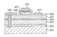
- FIG. 4is a sectional view showing a nitride semiconductor device according to a second embodiment of the present invention.
- the nitride semiconductor deviceincludes an n-type Si substrate 401 , an AlN buffer layer 402 , an underlying undoped AlGaN layer 403 , an undoped GaN layer 404 , an undoped AlGaN layer 405 , a p-type control layer 406 , and a p-type contact layer 407 .
- the n-type Si substrate 401has the (111) plane as a principal plane.
- the AlN buffer layer 402is provided on the (111) plane of the n-type Si substrate 401 .
- the underlying undoped AlGaN layer 403is provided on the AlN buffer layer 402 .
- the undoped GaN layer 404is provided on the underlying undoped AlGaN layer 403 .
- the undoped AlGaN layer 405is provided on the undoped GaN layer 404 .
- the p-type control layer 406is provided on a portion of the undoped AlGaN layer 405 , and made of AlGaN containing p-type impurities.
- the p-type contact layer 407is provided on the p-type control layer 406 , and made of GaN containing p-type impurities with a higher concentration than those in the p-type control layer 406 .
- the nitride semiconductor deviceincludes a gate electrode 411 , a source electrode 409 , a drain electrode 410 , and a passivation film 408 .
- the gate electrode 411 of Niis provided on the p-type contact layer 407 , and comes into ohmic contact with the p-type contact layer 407 .
- the source electrode 409 and the drain electrode 410are made of a Ti layer and an Al layer provided on the undoped AlGaN layer 405 .
- the passivation film 408is made of SiN, and covers the top surface of the undoped AlGaN layer 405 .
- the underlying undoped AlGaN layer 403 , the undoped AlGaN layer 405 , and the p-type control layer 406are both made of Al 0.2 Ga 0.8 N, but these layers may have different Al compositions.
- the band gaps of the underlying undoped AlGaN layer 403 and the undoped AlGaN layer 405are larger than the band gap of the undoped GaN layer 404 , so that the device has a so-called double hetero structure.
- the AlN buffer layer 402has a thickness of, for example, 40 nm
- the underlying undoped AlGaN layer 403has a thickness of, for example, 1 ⁇ m
- the undoped GaN layer 404has a thickness of, for example, 3 nm
- the undoped AlGaN layer 405has a thickness of, for example, 25 nm.
- the p-type control layer 406has a thickness of, for example, 100 nm
- the p-type contact layer 407has a thickness of, for example, 5 nm.
- the concentrations of p-type impurities (Mg) contained in the p-type control layer 406 and the p-type contact layer 407are the same as those of the nitride semiconductor device of the first embodiment.
- the source electrode 409is connected to the n-type Si substrate 401 through a via penetrating the undoped AlGaN layer 405 , the undoped GaN layer 404 , and the underlying undoped AlGaN layer 403 .
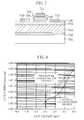
- FIG. 5is a graph showing the relation between the voltage (the gate voltage Vgs) applied to the control region (the gate region) and the drain current in the nitride semiconductor device of the second embodiment
- FIG. 6is a graph showing the relation between the source-drain voltage and the drain current in the case where the voltage applied to the control region is changed in the nitride semiconductor device of the second embodiment.
- the result of the measurement obtained from the nitride semiconductor device according to the first embodiment(the dotted curve in this figure) is also shown for comparison purposes.
- the nitride semiconductor device of the second embodimenthas a threshold voltage of about 2 V and exhibits normally-off characteristics.
- a positive bias of 7 V or higheris applied to the gate electrode 411 , no gate leakage current flows and a drain current of about 270 mA/mm at the maximum can be provided.
- the undoped GaN layer 404 acting as a channelis vertically sandwiched by the AlGaN layers with an Al mole fraction of 20%.
- the effect of spontaneous polarizationis compensated to produce the state in which no carrier is present.
- the nitride semiconductor device according to the second embodimenthas a higher threshold voltage than the nitride semiconductor device according to the first embodiment.
- the drain currentsharply increases.
- the drain current obtained in applying the control voltageis generated entirely by holes flowing from the p-type control layer 406 . This will be the reason why a kink of the electrical properties is not observed which is seen in the case where the undoped GaN layer is provided below the undoped AlGaN layer.
- the nitride semiconductor device of the second embodimentcan provide a higher drain current than the nitride semiconductor device of the first embodiment.
- the underlying undoped AlGaN layer 403 and the undoped AlGaN layer 405 provided on the top and bottom of the undoped GaN layer 404are set to have the same Al mole fraction.
- the underlying undoped AlGaN layer 403is set to have a lower Al mole fraction than the undoped AlGaN layer 405 , provision of the p-type control layer 406 can raise the potential of the channel portion to attain the normally-off characteristics.
- a normally-off type devicecan be provided in which only the holes are injected as mentioned above to flow the drain current and confinement of holes within the channel is promoted to flow a larger operating current.
- FIG. 7is a sectional view showing a nitride semiconductor device according to a third embodiment of the present invention.
- the nitride semiconductor deviceincludes a sapphire substrate 701 , an AlN buffer layer 702 , an undoped GaN layer 703 , an undoped AlGaN layer 704 , a lightly doped p-type control layer 705 , a heavily doped p-type control layer 706 , and a p-type contact layer 707 .
- the sapphire substrate 701has the (0001) plane as a principal plane.
- the AlN buffer layer 702is provided on the (0001) plane of the sapphire substrate 701 .
- the undoped GaN layer 703is provided on the AlN buffer layer 702 .
- the undoped AlGaN layer 704is provided on the undoped GaN layer 703 .
- the lightly doped p-type control layer 705is provided on a portion of the undoped AlGaN layer 704 , and made of AlGaN containing p-type impurities.
- the heavily doped p-type control layer 706is provided on the lightly doped p-type control layer 705 , and contains p-type impurities with a higher concentration than the lightly doped p-type control layer 705 .
- the p-type contact layer 707is provided on the heavily doped p-type control layer 706 , and made of GaN containing p-type impurities with a higher concentration than the heavily doped p-type control layer 706 .
- the nitride semiconductor deviceincludes a gate electrode 711 , a source electrode 709 , a drain electrode 710 , and a passivation film 708 .
- the gate electrode 711is provided on the p-type contact layer 707 .
- the source electrode 709 and the drain electrode 710are provided on the undoped AlGaN layer 704 .
- the passivation film 708covers the top surface of the undoped AlGaN layer 704 .
- the nitride semiconductor device according to the third embodimentis characterized in that the p-type control layer is divided into the lightly doped p-type control layer 705 and the heavily doped p-type control layer 706 and that the p-type control layer in contact with the undoped AlGaN layer has a lower impurity concentration than those of the first and second nitride semiconductor devices.
- the other structure thereofis the same as the structure of the nitride semiconductor device of the first embodiment.
- Both of the lightly doped p-type control layer 705 and the heavily doped p-type control layer 706have a thickness of 50 nm, and are made of Al 0.2 Ga 0.8 N.
- the lightly doped p-type control layer 705is doped with Mg with an impurity concentration of about 5 ⁇ 10 18 cm ⁇ 3
- the heavily doped p-type control layer 706is doped with Mg with an impurity concentration of about 1 ⁇ 10 19 cm ⁇ 3
- the p-type contact layer 707is doped with Mg with an impurity concentration of about 1 ⁇ 10 20 cm ⁇ 3 .
- FIG. 8is a graph showing the relation between the voltage (the gate voltage Vgs) applied to the control region and the current flowing through the gate electrode (the gate current Igs) in the nitride semiconductor device of the third embodiment.
- the solid curverepresents the electrical properties of the nitride semiconductor device of the third embodiment in which a Mg concentration profile is provided to the p-type control layer
- the dotted curverepresents the electrical properties of the nitride semiconductor device of the first embodiment in which no Mg concentration profile is provided to the p-type control layer.
- leakage current flowing in the gate electrode 711remarkably decreases as compared with the case where the lightly doped p-type control layer 705 is not provided. This is probably because provision of the lightly doped p-type control layer 705 can reduce leakage current flowing through Mg-involved traps.
- an increased operating current and a decreased leakage currentcan be provided even by the normally-off type device.
- the transistor according to the present inventionhas structural similarity to the JFET, and in addition holes can be injected one-directionally from the wide band-gap region through the heterojunction into the channel.
- the drain currentcan be increased significantly.
- the nitride semiconductorhas an extremely lower hole mobility than the electron mobility, the injected holes effectively serve only to increase the electron concentration in the channel. This eliminates device-design tradeoffs in which provision of normally-off characteristics inevitably causes a decrease in drain current.
- the transistor according to the present inventioncan be utilized as, for example, a power transistor with a high breakdown voltage for use in various types of switching equipment.
Landscapes
- Junction Field-Effect Transistors (AREA)
Abstract
Description
Claims (5)
Applications Claiming Priority (3)
| Application Number | Priority Date | Filing Date | Title |
|---|---|---|---|
| JP2005-200127 | 2005-07-08 | ||
| JP2005200127AJP4712459B2 (en) | 2005-07-08 | 2005-07-08 | Transistor and method of operating the same |
| PCT/JP2006/312830WO2007007548A1 (en) | 2005-07-08 | 2006-06-27 | Transistor and method for operating same |
Publications (2)
| Publication Number | Publication Date |
|---|---|
| US20090121775A1 US20090121775A1 (en) | 2009-05-14 |
| US8076698B2true US8076698B2 (en) | 2011-12-13 |
Family
ID=37636944
Family Applications (1)
| Application Number | Title | Priority Date | Filing Date |
|---|---|---|---|
| US11/995,040Active2026-07-22US8076698B2 (en) | 2005-07-08 | 2006-06-27 | Transistor and method for operating the same |
Country Status (5)
| Country | Link |
|---|---|
| US (1) | US8076698B2 (en) |
| EP (1) | EP1909316A4 (en) |
| JP (1) | JP4712459B2 (en) |
| CN (1) | CN101185158A (en) |
| WO (1) | WO2007007548A1 (en) |
Cited By (26)
| Publication number | Priority date | Publication date | Assignee | Title |
|---|---|---|---|---|
| US8569797B2 (en) | 2009-01-22 | 2013-10-29 | Panasonic Corporation | Field effect transistor and method of manufacturing the same |
| US8581300B2 (en) | 2011-09-26 | 2013-11-12 | Fujitsu Limited | Compound semiconductor device and method of manufacturing the same |
| US8587030B2 (en) | 2011-09-28 | 2013-11-19 | Fujitsu Limited | Compound semiconductor device and method of manufacturing the same |
| US20140103459A1 (en)* | 2011-07-15 | 2014-04-17 | Panasonic Corporation | Semiconductor device and method for fabricating the same |
| US8748861B2 (en) | 2010-03-01 | 2014-06-10 | Fujitsu Limited | Compound semiconductor device and method for manufacturing the same |
| US20140266411A1 (en)* | 2013-03-14 | 2014-09-18 | Panasonic Corporation | Switching device |
| US8890206B2 (en) | 2012-03-19 | 2014-11-18 | Transphorm Japan, Inc. | Compound semiconductor device and method for manufacturing the same |
| US9093366B2 (en) | 2012-04-09 | 2015-07-28 | Transphorm Inc. | N-polar III-nitride transistors |
| US9099351B2 (en) | 2012-09-21 | 2015-08-04 | Transphorm Japan, Inc. | Compound semiconductor device and method of manufacturing the same |
| US9171836B2 (en) | 2011-10-07 | 2015-10-27 | Transphorm Inc. | Method of forming electronic components with increased reliability |
| US9245993B2 (en) | 2013-03-15 | 2016-01-26 | Transphorm Inc. | Carbon doping semiconductor devices |
| US9318593B2 (en) | 2014-07-21 | 2016-04-19 | Transphorm Inc. | Forming enhancement mode III-nitride devices |
| US9397657B1 (en) | 2014-07-24 | 2016-07-19 | Eaton Corporation | Methods and systems for operating hybrid power devices using multiple current-dependent switching patterns |
| US9443938B2 (en) | 2013-07-19 | 2016-09-13 | Transphorm Inc. | III-nitride transistor including a p-type depleting layer |
| US9536967B2 (en) | 2014-12-16 | 2017-01-03 | Transphorm Inc. | Recessed ohmic contacts in a III-N device |
| US9536966B2 (en) | 2014-12-16 | 2017-01-03 | Transphorm Inc. | Gate structures for III-N devices |
| US9590060B2 (en) | 2013-03-13 | 2017-03-07 | Transphorm Inc. | Enhancement-mode III-nitride devices |
| US9722581B2 (en) | 2014-07-24 | 2017-08-01 | Eaton Corporation | Methods and systems for operating hybrid power devices using driver circuits that perform indirect instantaneous load current sensing |
| US10096702B2 (en) | 2016-06-01 | 2018-10-09 | Efficient Power Conversion Corporation | Multi-step surface passivation structures and methods for fabricating same |
| US10224401B2 (en) | 2016-05-31 | 2019-03-05 | Transphorm Inc. | III-nitride devices including a graded depleting layer |
| US20200006322A1 (en)* | 2018-06-29 | 2020-01-02 | Intel Corporation | Schottky diode structures and integration with iii-v transistors |
| US11121245B2 (en) | 2019-02-22 | 2021-09-14 | Efficient Power Conversion Corporation | Field plate structures with patterned surface passivation layers and methods for manufacturing thereof |
| US20220130988A1 (en)* | 2020-10-27 | 2022-04-28 | Texas Instruments Incorporated | Electronic device with enhancement mode gallium nitride transistor, and method of making same |
| US11322599B2 (en) | 2016-01-15 | 2022-05-03 | Transphorm Technology, Inc. | Enhancement mode III-nitride devices having an Al1-xSixO gate insulator |
| US11749740B2 (en)* | 2019-12-06 | 2023-09-05 | United Microelectronics Corp. | High electron mobility transistor and method for fabricating the same |
| WO2024151571A1 (en) | 2023-01-09 | 2024-07-18 | Efficient Power Conversion Corporation | GaN DEVICE WITH UNIFORM ELECTRIC FIELD |
Families Citing this family (62)
| Publication number | Priority date | Publication date | Assignee | Title |
|---|---|---|---|---|
| JP4705481B2 (en)* | 2006-01-25 | 2011-06-22 | パナソニック株式会社 | Nitride semiconductor device |
| JP4705482B2 (en)* | 2006-01-27 | 2011-06-22 | パナソニック株式会社 | Transistor |
| JP5147197B2 (en)* | 2006-06-06 | 2013-02-20 | パナソニック株式会社 | Transistor |
| JP2007329350A (en)* | 2006-06-08 | 2007-12-20 | Matsushita Electric Ind Co Ltd | Semiconductor device |
| JP4755961B2 (en)* | 2006-09-29 | 2011-08-24 | パナソニック株式会社 | Nitride semiconductor device and manufacturing method thereof |
| JP5186096B2 (en)* | 2006-10-12 | 2013-04-17 | パナソニック株式会社 | Nitride semiconductor transistor and manufacturing method thereof |
| US7679104B2 (en)* | 2006-11-09 | 2010-03-16 | The Furukawa Electric Co., Ltd. | Vertical type semiconductor device and manufacturing method of the device |
| WO2008062800A1 (en)* | 2006-11-20 | 2008-05-29 | Panasonic Corporation | Semiconductor device and its drive method |
| JP2008153748A (en)* | 2006-12-14 | 2008-07-03 | Matsushita Electric Ind Co Ltd | Bidirectional switch and bidirectional switch driving method |
| JP4712683B2 (en)* | 2006-12-21 | 2011-06-29 | パナソニック株式会社 | Transistor and manufacturing method thereof |
| US7838904B2 (en)* | 2007-01-31 | 2010-11-23 | Panasonic Corporation | Nitride based semiconductor device with concave gate region |
| US7531854B2 (en)* | 2007-05-04 | 2009-05-12 | Dsm Solutions, Inc. | Semiconductor device having strain-inducing substrate and fabrication methods thereof |
| WO2009001529A1 (en)* | 2007-06-22 | 2008-12-31 | Panasonic Corporation | Plasma display panel driving device and plasma display |
| JP5466505B2 (en)* | 2007-06-27 | 2014-04-09 | ルネサスエレクトロニクス株式会社 | FIELD EFFECT TRANSISTOR AND MULTILAYER EPITAXIAL FILM FOR MANUFACTURING THE FIELD EFFECT TRANSISTOR |
| US20090072269A1 (en)* | 2007-09-17 | 2009-03-19 | Chang Soo Suh | Gallium nitride diodes and integrated components |
| JP5433214B2 (en)* | 2007-12-07 | 2014-03-05 | パナソニック株式会社 | Motor drive circuit |
| JP5032965B2 (en)* | 2007-12-10 | 2012-09-26 | パナソニック株式会社 | Nitride semiconductor transistor and manufacturing method thereof |
| JP2009164158A (en)* | 2007-12-28 | 2009-07-23 | Panasonic Corp | Semiconductor device and manufacturing method thereof |
| JP2009200395A (en) | 2008-02-25 | 2009-09-03 | Sanken Electric Co Ltd | HFET and manufacturing method thereof |
| US8519438B2 (en) | 2008-04-23 | 2013-08-27 | Transphorm Inc. | Enhancement mode III-N HEMTs |
| JP5597921B2 (en) | 2008-12-22 | 2014-10-01 | サンケン電気株式会社 | Semiconductor device |
| JP5457046B2 (en)* | 2009-02-13 | 2014-04-02 | パナソニック株式会社 | Semiconductor device |
| US8742459B2 (en) | 2009-05-14 | 2014-06-03 | Transphorm Inc. | High voltage III-nitride semiconductor devices |
| US8390000B2 (en) | 2009-08-28 | 2013-03-05 | Transphorm Inc. | Semiconductor devices with field plates |
| JP5530682B2 (en)* | 2009-09-03 | 2014-06-25 | パナソニック株式会社 | Nitride semiconductor device |
| US8389977B2 (en)* | 2009-12-10 | 2013-03-05 | Transphorm Inc. | Reverse side engineered III-nitride devices |
| JP2011233751A (en)* | 2010-04-28 | 2011-11-17 | Panasonic Corp | Nitride semiconductor transistor |
| JP5672868B2 (en) | 2010-08-31 | 2015-02-18 | 富士通株式会社 | Compound semiconductor device and manufacturing method thereof |
| JP5810518B2 (en) | 2010-12-03 | 2015-11-11 | 富士通株式会社 | Compound semiconductor device and manufacturing method thereof |
| US8742460B2 (en) | 2010-12-15 | 2014-06-03 | Transphorm Inc. | Transistors with isolation regions |
| US8643062B2 (en) | 2011-02-02 | 2014-02-04 | Transphorm Inc. | III-N device structures and methods |
| JP5775321B2 (en) | 2011-02-17 | 2015-09-09 | トランスフォーム・ジャパン株式会社 | Semiconductor device, manufacturing method thereof, and power supply device |
| JP5913816B2 (en) | 2011-02-21 | 2016-04-27 | 富士通株式会社 | Manufacturing method of semiconductor device |
| US8772842B2 (en) | 2011-03-04 | 2014-07-08 | Transphorm, Inc. | Semiconductor diodes with low reverse bias currents |
| CN103548127B (en) | 2011-06-13 | 2016-12-07 | 松下知识产权经营株式会社 | Semiconductor device and manufacturing method thereof |
| JP2013074068A (en)* | 2011-09-27 | 2013-04-22 | Fujitsu Ltd | Semiconductor device and manufacturing method of semiconductor device |
| JP5890991B2 (en)* | 2011-09-28 | 2016-03-22 | トランスフォーム・ジャパン株式会社 | Compound semiconductor device and manufacturing method thereof |
| JP2013207107A (en)* | 2012-03-28 | 2013-10-07 | Fujitsu Ltd | Compound semiconductor device and method for manufacturing the same |
| CN102709321A (en)* | 2012-04-20 | 2012-10-03 | 程凯 | Enhanced switching device and manufacturing method thereof |
| US9184275B2 (en) | 2012-06-27 | 2015-11-10 | Transphorm Inc. | Semiconductor devices with integrated hole collectors |
| JP2014060358A (en)* | 2012-09-19 | 2014-04-03 | Toshiba Corp | Semiconductor device |
| JP2014072377A (en) | 2012-09-28 | 2014-04-21 | Fujitsu Ltd | Compound semiconductor device and manufacturing method of the same |
| JP6017248B2 (en) | 2012-09-28 | 2016-10-26 | トランスフォーム・ジャパン株式会社 | Semiconductor device manufacturing method and semiconductor device |
| JP2014072426A (en) | 2012-09-28 | 2014-04-21 | Fujitsu Ltd | Semiconductor device and semiconductor device manufacturing method |
| JP5949527B2 (en) | 2012-12-21 | 2016-07-06 | 富士通株式会社 | Semiconductor device and manufacturing method thereof, power supply device, and high-frequency amplifier |
| CN105164811B (en) | 2013-02-15 | 2018-08-31 | 创世舫电子有限公司 | Electrode of semiconductor devices and forming method thereof |
| TWI511294B (en)* | 2013-07-25 | 2015-12-01 | Vanguard Int Semiconduct Corp | Semiconduvtor device and methods for forming the same |
| US20150041820A1 (en)* | 2013-08-12 | 2015-02-12 | Philippe Renaud | Complementary gallium nitride integrated circuits and methods of their fabrication |
| CN106170866A (en)* | 2014-04-25 | 2016-11-30 | 美国休斯研究所 | There is the FET transistor on the III V race material structure of base material transfer |
| US9425301B2 (en)* | 2014-04-30 | 2016-08-23 | Taiwan Semiconductor Manufacturing Co., Ltd. | Sidewall passivation for HEMT devices |
| US10090406B2 (en)* | 2014-09-18 | 2018-10-02 | Infineon Technologies Austria Ag | Non-planar normally off compound semiconductor device |
| JP6223938B2 (en) | 2014-09-19 | 2017-11-01 | 株式会社東芝 | Gate control device, semiconductor device, and control method of semiconductor device |
| US9741711B2 (en) | 2014-10-28 | 2017-08-22 | Semiconductor Components Industries, Llc | Cascode semiconductor device structure and method therefor |
| JP6631950B2 (en) | 2014-12-11 | 2020-01-15 | パナソニックIpマネジメント株式会社 | Nitride semiconductor device and method of manufacturing nitride semiconductor device |
| CN105810707B (en)* | 2014-12-31 | 2018-07-24 | 黄智方 | Structure of High Electron Mobility Light Emitting Transistor |
| US9502602B2 (en)* | 2014-12-31 | 2016-11-22 | National Tsing Hua University | Structure of high electron mobility light emitting transistor |
| JP6593294B2 (en)* | 2016-09-28 | 2019-10-23 | トヨタ自動車株式会社 | Semiconductor device |
| US11114543B2 (en)* | 2017-01-24 | 2021-09-07 | Taiwan Semiconductor Manufacturing Co., Ltd. | Group III-V device structure |
| EP3442026B1 (en)* | 2017-08-11 | 2023-03-08 | IMEC vzw | Gate for an enhancement-mode transistor |
| CN111490100B (en)* | 2020-04-16 | 2024-04-05 | 英诺赛科(珠海)科技有限公司 | Semiconductor device and method for manufacturing the same |
| CN111430459B (en)* | 2020-04-28 | 2023-10-13 | 上海航天测控通信研究所 | AlGaAs/GaAs high electron mobility transistor and preparation method |
| CN116153993A (en)* | 2021-11-23 | 2023-05-23 | 联华电子股份有限公司 | Semiconductor structure and forming method thereof |
Citations (14)
| Publication number | Priority date | Publication date | Assignee | Title |
|---|---|---|---|---|
| JPS61140181A (en) | 1984-12-12 | 1986-06-27 | Nec Corp | semiconductor equipment |
| JPS61230381A (en) | 1985-04-05 | 1986-10-14 | Nec Corp | Semiconductor device |
| JPS62211963A (en) | 1986-03-13 | 1987-09-17 | Fujitsu Ltd | Hetero-junction semiconductor device |
| JPH01183162A (en) | 1988-01-18 | 1989-07-20 | Toshiba Corp | semiconductor equipment |
| US4903091A (en) | 1985-04-05 | 1990-02-20 | Nec Corporation | Heterojunction transistor having bipolar characteristics |
| JPH11261053A (en) | 1998-03-09 | 1999-09-24 | Furukawa Electric Co Ltd:The | High mobility transistor |
| JP2000100828A (en) | 1998-09-18 | 2000-04-07 | Sony Corp | Semiconductor device and manufacturing method thereof |
| JP2003133332A (en) | 2001-10-24 | 2003-05-09 | Shin Etsu Handotai Co Ltd | Compound semiconductor element |
| JP2004221363A (en)* | 2003-01-16 | 2004-08-05 | Hitachi Cable Ltd | Epitaxial wafer for high-speed electron mobility transistor |
| JP2004273486A (en) | 2003-03-05 | 2004-09-30 | Mitsubishi Electric Corp | Semiconductor device and method of manufacturing the same |
| JP2005086102A (en) | 2003-09-10 | 2005-03-31 | Univ Nagoya | Field effect transistor and method for manufacturing field effect transistor |
| US20050133816A1 (en)* | 2003-12-19 | 2005-06-23 | Zhaoyang Fan | III-nitride quantum-well field effect transistors |
| US20050189559A1 (en) | 2004-02-27 | 2005-09-01 | Kabushiki Kaisha Toshiba | Semiconductor device |
| US20060060871A1 (en) | 2004-01-23 | 2006-03-23 | International Rectifier Corp. | Enhancement mode III-nitride FET |
Family Cites Families (2)
| Publication number | Priority date | Publication date | Assignee | Title |
|---|---|---|---|---|
| KR100571071B1 (en)* | 1996-12-04 | 2006-06-21 | 소니 가부시끼 가이샤 | Field effect transistor and method for manufacturing the same |
| US7078743B2 (en)* | 2003-05-15 | 2006-07-18 | Matsushita Electric Industrial Co., Ltd. | Field effect transistor semiconductor device |
- 2005
- 2005-07-08JPJP2005200127Apatent/JP4712459B2/ennot_activeExpired - Lifetime
- 2006
- 2006-06-27USUS11/995,040patent/US8076698B2/enactiveActive
- 2006-06-27CNCNA2006800187863Apatent/CN101185158A/enactivePending
- 2006-06-27EPEP06767447Apatent/EP1909316A4/ennot_activeCeased
- 2006-06-27WOPCT/JP2006/312830patent/WO2007007548A1/ennot_activeCeased
Patent Citations (17)
| Publication number | Priority date | Publication date | Assignee | Title |
|---|---|---|---|---|
| JPS61140181A (en) | 1984-12-12 | 1986-06-27 | Nec Corp | semiconductor equipment |
| US4839703A (en) | 1984-12-12 | 1989-06-13 | Nec Corporation | High speed and power transistor |
| JPS61230381A (en) | 1985-04-05 | 1986-10-14 | Nec Corp | Semiconductor device |
| US4903091A (en) | 1985-04-05 | 1990-02-20 | Nec Corporation | Heterojunction transistor having bipolar characteristics |
| JPS62211963A (en) | 1986-03-13 | 1987-09-17 | Fujitsu Ltd | Hetero-junction semiconductor device |
| JPH01183162A (en) | 1988-01-18 | 1989-07-20 | Toshiba Corp | semiconductor equipment |
| JPH11261053A (en) | 1998-03-09 | 1999-09-24 | Furukawa Electric Co Ltd:The | High mobility transistor |
| US6281528B1 (en) | 1998-09-18 | 2001-08-28 | Sony Corporation | Ohmic contact improvement between layer of a semiconductor device |
| JP2000100828A (en) | 1998-09-18 | 2000-04-07 | Sony Corp | Semiconductor device and manufacturing method thereof |
| JP2003133332A (en) | 2001-10-24 | 2003-05-09 | Shin Etsu Handotai Co Ltd | Compound semiconductor element |
| JP2004221363A (en)* | 2003-01-16 | 2004-08-05 | Hitachi Cable Ltd | Epitaxial wafer for high-speed electron mobility transistor |
| JP2004273486A (en) | 2003-03-05 | 2004-09-30 | Mitsubishi Electric Corp | Semiconductor device and method of manufacturing the same |
| JP2005086102A (en) | 2003-09-10 | 2005-03-31 | Univ Nagoya | Field effect transistor and method for manufacturing field effect transistor |
| US20050133816A1 (en)* | 2003-12-19 | 2005-06-23 | Zhaoyang Fan | III-nitride quantum-well field effect transistors |
| US20060060871A1 (en) | 2004-01-23 | 2006-03-23 | International Rectifier Corp. | Enhancement mode III-nitride FET |
| US20050189559A1 (en) | 2004-02-27 | 2005-09-01 | Kabushiki Kaisha Toshiba | Semiconductor device |
| US7038252B2 (en) | 2004-02-27 | 2006-05-02 | Kabushiki Kaisha Toshiba | Semiconductor device using a nitride semiconductor |
Non-Patent Citations (7)
| Title |
|---|
| Ambacher, O., et al., "Two-dimensional electron gases induced by spontaneous and piezoelectric polarization charges in N- and Ga-face AIGaN/GaN heterostructures", Journal of Applied Physics, Mar. 15, 2999, pages 3222-3233, vol. 85, No. 6, American institute of Physics. |
| European Search Report issued in European Patent Application No. 06767447.3, mailed May 8, 2009. |
| Hikita, M., et al., "350V/150A AlGaN/GaN power HFET on Silicon substrate with source-via grounding (SVG) structure", Technical Digest of International Electron Devices Meeting, 2004, pp. 803-806, IEEE. |
| Hu, X., et al., "Enhancement mode AIGaN/GaN HFET with selectively grown pn junction gate", Electronics Letters, Apr. 13, 2000, pp. 753-754, vol. 36 No. 8. |
| Japanese Notice of Reasons for Rejection, w/ English translation thereof, issued in Japanese Patent Application No. JP 2005-200127 dated Nov. 16, 2010. |
| Machine Translation of JP 11-261053.* |
| Zhang, L., et al., "Epitaxially-Grown GaN Junction Field Effect Transistors", IEEE Transactions on Electron Devices, Mar. 2000, pp. 507-511, vol. 47 No. 3, IEEE. |
Cited By (42)
| Publication number | Priority date | Publication date | Assignee | Title |
|---|---|---|---|---|
| US8569797B2 (en) | 2009-01-22 | 2013-10-29 | Panasonic Corporation | Field effect transistor and method of manufacturing the same |
| US8748861B2 (en) | 2010-03-01 | 2014-06-10 | Fujitsu Limited | Compound semiconductor device and method for manufacturing the same |
| US9071167B2 (en) | 2010-03-01 | 2015-06-30 | Fujitsu Limited | Compound semiconductor device and method for manufacturing the same |
| US20140103459A1 (en)* | 2011-07-15 | 2014-04-17 | Panasonic Corporation | Semiconductor device and method for fabricating the same |
| US9842905B2 (en)* | 2011-07-15 | 2017-12-12 | Panasonic Intellectual Property Management Co., Ltd. | Semiconductor device and method for fabricating the same |
| US8581300B2 (en) | 2011-09-26 | 2013-11-12 | Fujitsu Limited | Compound semiconductor device and method of manufacturing the same |
| US8587030B2 (en) | 2011-09-28 | 2013-11-19 | Fujitsu Limited | Compound semiconductor device and method of manufacturing the same |
| US9171836B2 (en) | 2011-10-07 | 2015-10-27 | Transphorm Inc. | Method of forming electronic components with increased reliability |
| US8890206B2 (en) | 2012-03-19 | 2014-11-18 | Transphorm Japan, Inc. | Compound semiconductor device and method for manufacturing the same |
| US9490324B2 (en) | 2012-04-09 | 2016-11-08 | Transphorm Inc. | N-polar III-nitride transistors |
| US9093366B2 (en) | 2012-04-09 | 2015-07-28 | Transphorm Inc. | N-polar III-nitride transistors |
| US9099351B2 (en) | 2012-09-21 | 2015-08-04 | Transphorm Japan, Inc. | Compound semiconductor device and method of manufacturing the same |
| US9590060B2 (en) | 2013-03-13 | 2017-03-07 | Transphorm Inc. | Enhancement-mode III-nitride devices |
| US10535763B2 (en) | 2013-03-13 | 2020-01-14 | Transphorm Inc. | Enhancement-mode III-nitride devices |
| US10043898B2 (en) | 2013-03-13 | 2018-08-07 | Transphorm Inc. | Enhancement-mode III-nitride devices |
| US8896369B2 (en)* | 2013-03-14 | 2014-11-25 | Panasonic Coporation | Switching device |
| US20140266411A1 (en)* | 2013-03-14 | 2014-09-18 | Panasonic Corporation | Switching device |
| US9245992B2 (en) | 2013-03-15 | 2016-01-26 | Transphorm Inc. | Carbon doping semiconductor devices |
| US9245993B2 (en) | 2013-03-15 | 2016-01-26 | Transphorm Inc. | Carbon doping semiconductor devices |
| US9865719B2 (en) | 2013-03-15 | 2018-01-09 | Transphorm Inc. | Carbon doping semiconductor devices |
| US10043896B2 (en) | 2013-07-19 | 2018-08-07 | Transphorm Inc. | III-Nitride transistor including a III-N depleting layer |
| US9842922B2 (en) | 2013-07-19 | 2017-12-12 | Transphorm Inc. | III-nitride transistor including a p-type depleting layer |
| US9443938B2 (en) | 2013-07-19 | 2016-09-13 | Transphorm Inc. | III-nitride transistor including a p-type depleting layer |
| US9935190B2 (en) | 2014-07-21 | 2018-04-03 | Transphorm Inc. | Forming enhancement mode III-nitride devices |
| US9318593B2 (en) | 2014-07-21 | 2016-04-19 | Transphorm Inc. | Forming enhancement mode III-nitride devices |
| US9722581B2 (en) | 2014-07-24 | 2017-08-01 | Eaton Corporation | Methods and systems for operating hybrid power devices using driver circuits that perform indirect instantaneous load current sensing |
| US10020802B2 (en) | 2014-07-24 | 2018-07-10 | Eaton Intelligent Power Limited | Methods and systems for operating hybrid power devices using driver circuits that perform indirect instantaneous load current sensing using stored I-V characteristics |
| US9397657B1 (en) | 2014-07-24 | 2016-07-19 | Eaton Corporation | Methods and systems for operating hybrid power devices using multiple current-dependent switching patterns |
| US9536966B2 (en) | 2014-12-16 | 2017-01-03 | Transphorm Inc. | Gate structures for III-N devices |
| US9536967B2 (en) | 2014-12-16 | 2017-01-03 | Transphorm Inc. | Recessed ohmic contacts in a III-N device |
| US11322599B2 (en) | 2016-01-15 | 2022-05-03 | Transphorm Technology, Inc. | Enhancement mode III-nitride devices having an Al1-xSixO gate insulator |
| US10224401B2 (en) | 2016-05-31 | 2019-03-05 | Transphorm Inc. | III-nitride devices including a graded depleting layer |
| US10629681B2 (en) | 2016-05-31 | 2020-04-21 | Transphorm Technology, Inc. | III-nitride devices including a graded depleting layer |
| US11121216B2 (en) | 2016-05-31 | 2021-09-14 | Transphorm Technology, Inc. | III-nitride devices including a graded depleting layer |
| DE112017002778T5 (en) | 2016-06-01 | 2019-02-14 | Efficient Power Conversion Corporation | Multi-stage surface passivation structures and methods for their preparation |
| US10096702B2 (en) | 2016-06-01 | 2018-10-09 | Efficient Power Conversion Corporation | Multi-step surface passivation structures and methods for fabricating same |
| US20200006322A1 (en)* | 2018-06-29 | 2020-01-02 | Intel Corporation | Schottky diode structures and integration with iii-v transistors |
| US11521964B2 (en)* | 2018-06-29 | 2022-12-06 | Intel Corporation | Schottky diode structures and integration with III-V transistors |
| US11121245B2 (en) | 2019-02-22 | 2021-09-14 | Efficient Power Conversion Corporation | Field plate structures with patterned surface passivation layers and methods for manufacturing thereof |
| US11749740B2 (en)* | 2019-12-06 | 2023-09-05 | United Microelectronics Corp. | High electron mobility transistor and method for fabricating the same |
| US20220130988A1 (en)* | 2020-10-27 | 2022-04-28 | Texas Instruments Incorporated | Electronic device with enhancement mode gallium nitride transistor, and method of making same |
| WO2024151571A1 (en) | 2023-01-09 | 2024-07-18 | Efficient Power Conversion Corporation | GaN DEVICE WITH UNIFORM ELECTRIC FIELD |
Also Published As
| Publication number | Publication date |
|---|---|
| WO2007007548A1 (en) | 2007-01-18 |
| CN101185158A (en) | 2008-05-21 |
| JP4712459B2 (en) | 2011-06-29 |
| US20090121775A1 (en) | 2009-05-14 |
| EP1909316A4 (en) | 2009-06-03 |
| JP2007019309A (en) | 2007-01-25 |
| EP1909316A1 (en) | 2008-04-09 |
Similar Documents
| Publication | Publication Date | Title |
|---|---|---|
| US8076698B2 (en) | Transistor and method for operating the same | |
| US7816707B2 (en) | Field-effect transistor with nitride semiconductor and method for fabricating the same | |
| US7576373B1 (en) | Nitride semiconductor device and method for manufacturing the same | |
| US8390029B2 (en) | Semiconductor device for reducing and/or preventing current collapse | |
| US6914273B2 (en) | GaN-type enhancement MOSFET using hetero structure | |
| US8164115B2 (en) | Nitride semiconductor device | |
| US6555851B2 (en) | High electron mobility transistor | |
| US8148752B2 (en) | Field effect transistor | |
| JP4705481B2 (en) | Nitride semiconductor device | |
| US8129748B2 (en) | Nitride semiconductor device and method for fabricating the same | |
| JP5469098B2 (en) | Field effect transistor and manufacturing method thereof | |
| US9589951B2 (en) | High-electron-mobility transistor with protective diode | |
| KR20070003906A (en) | Nitride heterojunction transistors having an energy barrier induced by charge-transfer and a method of manufacturing the same | |
| US20120274402A1 (en) | High electron mobility transistor | |
| JP2011066464A (en) | Field effect transistor | |
| JP2011142358A (en) | Nitride semiconductor device | |
| JP2013239735A (en) | Field effect transistor |
Legal Events
| Date | Code | Title | Description |
|---|---|---|---|
| AS | Assignment | Owner name:MATSUSHITA ELECTRIC INDUSTRIAL CO., LTD., JAPAN Free format text:ASSIGNMENT OF ASSIGNORS INTEREST;ASSIGNORS:UEDA, DAISUKE;TANAKA, TSUYOSHI;UEMOTO, YASUHIRO;AND OTHERS;REEL/FRAME:020818/0813;SIGNING DATES FROM 20071226 TO 20071227 Owner name:MATSUSHITA ELECTRIC INDUSTRIAL CO., LTD., JAPAN Free format text:ASSIGNMENT OF ASSIGNORS INTEREST;ASSIGNORS:UEDA, DAISUKE;TANAKA, TSUYOSHI;UEMOTO, YASUHIRO;AND OTHERS;SIGNING DATES FROM 20071226 TO 20071227;REEL/FRAME:020818/0813 | |
| AS | Assignment | Owner name:PANASONIC CORPORATION, JAPAN Free format text:CHANGE OF NAME;ASSIGNOR:MATSUSHITA ELECTRIC INDUSTRIAL CO., LTD.;REEL/FRAME:021832/0197 Effective date:20081001 Owner name:PANASONIC CORPORATION,JAPAN Free format text:CHANGE OF NAME;ASSIGNOR:MATSUSHITA ELECTRIC INDUSTRIAL CO., LTD.;REEL/FRAME:021832/0197 Effective date:20081001 | |
| FEPP | Fee payment procedure | Free format text:PAYOR NUMBER ASSIGNED (ORIGINAL EVENT CODE: ASPN); ENTITY STATUS OF PATENT OWNER: LARGE ENTITY | |
| STCF | Information on status: patent grant | Free format text:PATENTED CASE | |
| FPAY | Fee payment | Year of fee payment:4 | |
| MAFP | Maintenance fee payment | Free format text:PAYMENT OF MAINTENANCE FEE, 8TH YEAR, LARGE ENTITY (ORIGINAL EVENT CODE: M1552); ENTITY STATUS OF PATENT OWNER: LARGE ENTITY Year of fee payment:8 | |
| MAFP | Maintenance fee payment | Free format text:PAYMENT OF MAINTENANCE FEE, 12TH YEAR, LARGE ENTITY (ORIGINAL EVENT CODE: M1553); ENTITY STATUS OF PATENT OWNER: LARGE ENTITY Year of fee payment:12 | |
| AS | Assignment | Owner name:PANASONIC HOLDINGS CORPORATION, JAPAN Free format text:CHANGE OF NAME;ASSIGNOR:PANASONIC CORPORATION;REEL/FRAME:069631/0392 Effective date:20220401 |