US8076237B2 - Method and apparatus for 3D interconnect - Google Patents
Method and apparatus for 3D interconnectDownload PDFInfo
- Publication number
- US8076237B2 US8076237B2US12/118,596US11859608AUS8076237B2US 8076237 B2US8076237 B2US 8076237B2US 11859608 AUS11859608 AUS 11859608AUS 8076237 B2US8076237 B2US 8076237B2
- Authority
- US
- United States
- Prior art keywords
- cavity
- substrate
- conductive
- intracavity
- depositing
- Prior art date
- Legal status (The legal status is an assumption and is not a legal conclusion. Google has not performed a legal analysis and makes no representation as to the accuracy of the status listed.)
- Active, expires
Links
- 238000000034methodMethods0.000titleclaimsabstractdescription131
- 239000000758substrateSubstances0.000claimsabstractdescription163
- 239000000463materialSubstances0.000claimsabstractdescription75
- 239000004020conductorSubstances0.000claimsabstractdescription74
- 238000000151depositionMethods0.000claimsabstractdescription67
- 238000011049fillingMethods0.000claimsabstractdescription38
- 230000008021depositionEffects0.000claimsdescription39
- 230000004888barrier functionEffects0.000claimsdescription30
- 229910052751metalInorganic materials0.000claimsdescription24
- 239000002184metalSubstances0.000claimsdescription23
- 239000012212insulatorSubstances0.000claimsdescription19
- 229910052802copperInorganic materials0.000claimsdescription14
- 238000000638solvent extractionMethods0.000claimsdescription12
- 229910045601alloyInorganic materials0.000claimsdescription8
- 239000000956alloySubstances0.000claimsdescription8
- 238000004891communicationMethods0.000claimsdescription8
- 238000005530etchingMethods0.000claimsdescription8
- 229910052782aluminiumInorganic materials0.000claimsdescription6
- 229910052759nickelInorganic materials0.000claimsdescription6
- 229910052709silverInorganic materials0.000claimsdescription6
- 229910052721tungstenInorganic materials0.000claimsdescription6
- 238000003801millingMethods0.000claimsdescription5
- 229910052697platinumInorganic materials0.000claimsdescription3
- 229910052703rhodiumInorganic materials0.000claimsdescription3
- 239000002904solventSubstances0.000claimsdescription3
- ATJFFYVFTNAWJD-UHFFFAOYSA-NTinChemical compound[Sn]ATJFFYVFTNAWJD-UHFFFAOYSA-N0.000claimsdescription2
- 239000012811non-conductive materialSubstances0.000claimsdescription2
- 229910052715tantalumInorganic materials0.000claimsdescription2
- 239000003990capacitorSubstances0.000abstractdescription5
- 239000010410layerSubstances0.000description70
- 239000010949copperSubstances0.000description12
- 238000004519manufacturing processMethods0.000description12
- RYGMFSIKBFXOCR-UHFFFAOYSA-NCopperChemical compound[Cu]RYGMFSIKBFXOCR-UHFFFAOYSA-N0.000description11
- 238000007747platingMethods0.000description9
- 239000004065semiconductorSubstances0.000description9
- 239000000126substanceSubstances0.000description8
- PXHVJJICTQNCMI-UHFFFAOYSA-NnickelSubstances[Ni]PXHVJJICTQNCMI-UHFFFAOYSA-N0.000description7
- VYPSYNLAJGMNEJ-UHFFFAOYSA-NSilicium dioxideChemical compoundO=[Si]=OVYPSYNLAJGMNEJ-UHFFFAOYSA-N0.000description6
- 238000013459approachMethods0.000description6
- 239000011248coating agentSubstances0.000description6
- 238000000576coating methodMethods0.000description6
- 229910052737goldInorganic materials0.000description6
- 239000010931goldSubstances0.000description6
- 238000001020plasma etchingMethods0.000description6
- PCHJSUWPFVWCPO-UHFFFAOYSA-NgoldChemical compound[Au]PCHJSUWPFVWCPO-UHFFFAOYSA-N0.000description5
- 230000009467reductionEffects0.000description5
- 235000012431wafersNutrition0.000description5
- 238000005498polishingMethods0.000description4
- XUIMIQQOPSSXEZ-UHFFFAOYSA-NSiliconChemical compound[Si]XUIMIQQOPSSXEZ-UHFFFAOYSA-N0.000description3
- BQCADISMDOOEFD-UHFFFAOYSA-NSilverChemical compound[Ag]BQCADISMDOOEFD-UHFFFAOYSA-N0.000description3
- XAGFODPZIPBFFR-UHFFFAOYSA-NaluminiumChemical compound[Al]XAGFODPZIPBFFR-UHFFFAOYSA-N0.000description3
- 238000003491arrayMethods0.000description3
- 229910052681coesiteInorganic materials0.000description3
- 229910052906cristobaliteInorganic materials0.000description3
- 238000005137deposition processMethods0.000description3
- 238000004070electrodepositionMethods0.000description3
- 229910052738indiumInorganic materials0.000description3
- APFVFJFRJDLVQX-UHFFFAOYSA-Nindium atomChemical compound[In]APFVFJFRJDLVQX-UHFFFAOYSA-N0.000description3
- 230000010354integrationEffects0.000description3
- 238000005192partitionMethods0.000description3
- 238000000059patterningMethods0.000description3
- BASFCYQUMIYNBI-UHFFFAOYSA-NplatinumSubstances[Pt]BASFCYQUMIYNBI-UHFFFAOYSA-N0.000description3
- 229910052710siliconInorganic materials0.000description3
- 239000010703siliconSubstances0.000description3
- 239000000377silicon dioxideSubstances0.000description3
- 239000004332silverSubstances0.000description3
- 229910052682stishoviteInorganic materials0.000description3
- 229910052905tridymiteInorganic materials0.000description3
- WFKWXMTUELFFGS-UHFFFAOYSA-NtungstenChemical compound[W]WFKWXMTUELFFGS-UHFFFAOYSA-N0.000description3
- 239000010937tungstenSubstances0.000description3
- 239000011800void materialSubstances0.000description3
- 239000004593EpoxySubstances0.000description2
- 230000000712assemblyEffects0.000description2
- 238000000429assemblyMethods0.000description2
- 238000004140cleaningMethods0.000description2
- 238000009792diffusion processMethods0.000description2
- 238000007772electroless platingMethods0.000description2
- 239000011229interlayerSubstances0.000description2
- 238000001465metallisationMethods0.000description2
- 239000000615nonconductorSubstances0.000description2
- 238000004806packaging method and processMethods0.000description2
- 239000010948rhodiumSubstances0.000description2
- 229910019142PO4Inorganic materials0.000description1
- 239000004721Polyphenylene oxideSubstances0.000description1
- 239000000654additiveSubstances0.000description1
- 239000000853adhesiveSubstances0.000description1
- 230000001070adhesive effectEffects0.000description1
- PNEYBMLMFCGWSK-UHFFFAOYSA-Naluminium oxideInorganic materials[O-2].[O-2].[O-2].[Al+3].[Al+3]PNEYBMLMFCGWSK-UHFFFAOYSA-N0.000description1
- 230000005540biological transmissionEffects0.000description1
- 230000015572biosynthetic processEffects0.000description1
- 238000005266castingMethods0.000description1
- 238000003486chemical etchingMethods0.000description1
- 239000003795chemical substances by applicationSubstances0.000description1
- 230000000052comparative effectEffects0.000description1
- 239000002131composite materialSubstances0.000description1
- 239000013078crystalSubstances0.000description1
- 230000007547defectEffects0.000description1
- 230000002500effect on skinEffects0.000description1
- 230000000694effectsEffects0.000description1
- 238000009713electroplatingMethods0.000description1
- 238000005516engineering processMethods0.000description1
- 238000000605extractionMethods0.000description1
- 238000001125extrusionMethods0.000description1
- 238000005242forgingMethods0.000description1
- 238000005755formation reactionMethods0.000description1
- 230000014509gene expressionEffects0.000description1
- 230000005484gravityEffects0.000description1
- 238000003780insertionMethods0.000description1
- 230000037431insertionEffects0.000description1
- 238000001459lithographyMethods0.000description1
- 239000000314lubricantSubstances0.000description1
- 239000007769metal materialSubstances0.000description1
- 150000002739metalsChemical class0.000description1
- 238000004377microelectronicMethods0.000description1
- 230000003287optical effectEffects0.000description1
- TWNQGVIAIRXVLR-UHFFFAOYSA-Noxo(oxoalumanyloxy)alumaneChemical compoundO=[Al]O[Al]=OTWNQGVIAIRXVLR-UHFFFAOYSA-N0.000description1
- NBIIXXVUZAFLBC-UHFFFAOYSA-KphosphateChemical compound[O-]P([O-])([O-])=ONBIIXXVUZAFLBC-UHFFFAOYSA-K0.000description1
- 239000010452phosphateSubstances0.000description1
- 238000000206photolithographyMethods0.000description1
- 229920000570polyetherPolymers0.000description1
- 238000011160researchMethods0.000description1
- 229920005989resinPolymers0.000description1
- 239000011347resinSubstances0.000description1
- 230000000717retained effectEffects0.000description1
- 238000012552reviewMethods0.000description1
- MHOVAHRLVXNVSD-UHFFFAOYSA-Nrhodium atomChemical compound[Rh]MHOVAHRLVXNVSD-UHFFFAOYSA-N0.000description1
- 230000011664signalingEffects0.000description1
- 238000004544sputter depositionMethods0.000description1
- GUVRBAGPIYLISA-UHFFFAOYSA-Ntantalum atomChemical compound[Ta]GUVRBAGPIYLISA-UHFFFAOYSA-N0.000description1
- 239000001993waxSubstances0.000description1
- 238000003466weldingMethods0.000description1
Images


Classifications
- H—ELECTRICITY
- H05—ELECTRIC TECHNIQUES NOT OTHERWISE PROVIDED FOR
- H05K—PRINTED CIRCUITS; CASINGS OR CONSTRUCTIONAL DETAILS OF ELECTRIC APPARATUS; MANUFACTURE OF ASSEMBLAGES OF ELECTRICAL COMPONENTS
- H05K3/00—Apparatus or processes for manufacturing printed circuits
- H05K3/40—Forming printed elements for providing electric connections to or between printed circuits
- H05K3/4038—Through-connections; Vertical interconnect access [VIA] connections
- H—ELECTRICITY
- H01—ELECTRIC ELEMENTS
- H01L—SEMICONDUCTOR DEVICES NOT COVERED BY CLASS H10
- H01L21/00—Processes or apparatus adapted for the manufacture or treatment of semiconductor or solid state devices or of parts thereof
- H01L21/70—Manufacture or treatment of devices consisting of a plurality of solid state components formed in or on a common substrate or of parts thereof; Manufacture of integrated circuit devices or of parts thereof
- H01L21/71—Manufacture of specific parts of devices defined in group H01L21/70
- H01L21/768—Applying interconnections to be used for carrying current between separate components within a device comprising conductors and dielectrics
- H01L21/76838—Applying interconnections to be used for carrying current between separate components within a device comprising conductors and dielectrics characterised by the formation and the after-treatment of the conductors
- H01L21/76877—Filling of holes, grooves or trenches, e.g. vias, with conductive material
- H—ELECTRICITY
- H01—ELECTRIC ELEMENTS
- H01L—SEMICONDUCTOR DEVICES NOT COVERED BY CLASS H10
- H01L21/00—Processes or apparatus adapted for the manufacture or treatment of semiconductor or solid state devices or of parts thereof
- H01L21/70—Manufacture or treatment of devices consisting of a plurality of solid state components formed in or on a common substrate or of parts thereof; Manufacture of integrated circuit devices or of parts thereof
- H01L21/71—Manufacture of specific parts of devices defined in group H01L21/70
- H01L21/768—Applying interconnections to be used for carrying current between separate components within a device comprising conductors and dielectrics
- H01L21/76898—Applying interconnections to be used for carrying current between separate components within a device comprising conductors and dielectrics formed through a semiconductor substrate
- H—ELECTRICITY
- H01—ELECTRIC ELEMENTS
- H01L—SEMICONDUCTOR DEVICES NOT COVERED BY CLASS H10
- H01L23/00—Details of semiconductor or other solid state devices
- H01L23/48—Arrangements for conducting electric current to or from the solid state body in operation, e.g. leads, terminal arrangements ; Selection of materials therefor
- H01L23/481—Internal lead connections, e.g. via connections, feedthrough structures
- H—ELECTRICITY
- H01—ELECTRIC ELEMENTS
- H01L—SEMICONDUCTOR DEVICES NOT COVERED BY CLASS H10
- H01L24/00—Arrangements for connecting or disconnecting semiconductor or solid-state bodies; Methods or apparatus related thereto
- H01L24/01—Means for bonding being attached to, or being formed on, the surface to be connected, e.g. chip-to-package, die-attach, "first-level" interconnects; Manufacturing methods related thereto
- H01L24/02—Bonding areas ; Manufacturing methods related thereto
- H01L24/04—Structure, shape, material or disposition of the bonding areas prior to the connecting process
- H01L24/05—Structure, shape, material or disposition of the bonding areas prior to the connecting process of an individual bonding area
- H—ELECTRICITY
- H01—ELECTRIC ELEMENTS
- H01L—SEMICONDUCTOR DEVICES NOT COVERED BY CLASS H10
- H01L2224/00—Indexing scheme for arrangements for connecting or disconnecting semiconductor or solid-state bodies and methods related thereto as covered by H01L24/00
- H01L2224/01—Means for bonding being attached to, or being formed on, the surface to be connected, e.g. chip-to-package, die-attach, "first-level" interconnects; Manufacturing methods related thereto
- H01L2224/02—Bonding areas; Manufacturing methods related thereto
- H01L2224/04—Structure, shape, material or disposition of the bonding areas prior to the connecting process
- H01L2224/04042—Bonding areas specifically adapted for wire connectors, e.g. wirebond pads
- H—ELECTRICITY
- H01—ELECTRIC ELEMENTS
- H01L—SEMICONDUCTOR DEVICES NOT COVERED BY CLASS H10
- H01L2224/00—Indexing scheme for arrangements for connecting or disconnecting semiconductor or solid-state bodies and methods related thereto as covered by H01L24/00
- H01L2224/01—Means for bonding being attached to, or being formed on, the surface to be connected, e.g. chip-to-package, die-attach, "first-level" interconnects; Manufacturing methods related thereto
- H01L2224/02—Bonding areas; Manufacturing methods related thereto
- H01L2224/04—Structure, shape, material or disposition of the bonding areas prior to the connecting process
- H01L2224/05—Structure, shape, material or disposition of the bonding areas prior to the connecting process of an individual bonding area
- H01L2224/05001—Internal layers
- H01L2224/05075—Plural internal layers
- H01L2224/0508—Plural internal layers being stacked
- H01L2224/05085—Plural internal layers being stacked with additional elements, e.g. vias arrays, interposed between the stacked layers
- H01L2224/05089—Disposition of the additional element
- H01L2224/05093—Disposition of the additional element of a plurality of vias
- H—ELECTRICITY
- H01—ELECTRIC ELEMENTS
- H01L—SEMICONDUCTOR DEVICES NOT COVERED BY CLASS H10
- H01L2924/00—Indexing scheme for arrangements or methods for connecting or disconnecting semiconductor or solid-state bodies as covered by H01L24/00
- H01L2924/01—Chemical elements
- H01L2924/01005—Boron [B]
- H—ELECTRICITY
- H01—ELECTRIC ELEMENTS
- H01L—SEMICONDUCTOR DEVICES NOT COVERED BY CLASS H10
- H01L2924/00—Indexing scheme for arrangements or methods for connecting or disconnecting semiconductor or solid-state bodies as covered by H01L24/00
- H01L2924/01—Chemical elements
- H01L2924/01006—Carbon [C]
- H—ELECTRICITY
- H01—ELECTRIC ELEMENTS
- H01L—SEMICONDUCTOR DEVICES NOT COVERED BY CLASS H10
- H01L2924/00—Indexing scheme for arrangements or methods for connecting or disconnecting semiconductor or solid-state bodies as covered by H01L24/00
- H01L2924/01—Chemical elements
- H01L2924/01013—Aluminum [Al]
- H—ELECTRICITY
- H01—ELECTRIC ELEMENTS
- H01L—SEMICONDUCTOR DEVICES NOT COVERED BY CLASS H10
- H01L2924/00—Indexing scheme for arrangements or methods for connecting or disconnecting semiconductor or solid-state bodies as covered by H01L24/00
- H01L2924/01—Chemical elements
- H01L2924/01014—Silicon [Si]
- H—ELECTRICITY
- H01—ELECTRIC ELEMENTS
- H01L—SEMICONDUCTOR DEVICES NOT COVERED BY CLASS H10
- H01L2924/00—Indexing scheme for arrangements or methods for connecting or disconnecting semiconductor or solid-state bodies as covered by H01L24/00
- H01L2924/01—Chemical elements
- H01L2924/01015—Phosphorus [P]
- H—ELECTRICITY
- H01—ELECTRIC ELEMENTS
- H01L—SEMICONDUCTOR DEVICES NOT COVERED BY CLASS H10
- H01L2924/00—Indexing scheme for arrangements or methods for connecting or disconnecting semiconductor or solid-state bodies as covered by H01L24/00
- H01L2924/01—Chemical elements
- H01L2924/01022—Titanium [Ti]
- H—ELECTRICITY
- H01—ELECTRIC ELEMENTS
- H01L—SEMICONDUCTOR DEVICES NOT COVERED BY CLASS H10
- H01L2924/00—Indexing scheme for arrangements or methods for connecting or disconnecting semiconductor or solid-state bodies as covered by H01L24/00
- H01L2924/01—Chemical elements
- H01L2924/01023—Vanadium [V]
- H—ELECTRICITY
- H01—ELECTRIC ELEMENTS
- H01L—SEMICONDUCTOR DEVICES NOT COVERED BY CLASS H10
- H01L2924/00—Indexing scheme for arrangements or methods for connecting or disconnecting semiconductor or solid-state bodies as covered by H01L24/00
- H01L2924/01—Chemical elements
- H01L2924/01024—Chromium [Cr]
- H—ELECTRICITY
- H01—ELECTRIC ELEMENTS
- H01L—SEMICONDUCTOR DEVICES NOT COVERED BY CLASS H10
- H01L2924/00—Indexing scheme for arrangements or methods for connecting or disconnecting semiconductor or solid-state bodies as covered by H01L24/00
- H01L2924/01—Chemical elements
- H01L2924/01027—Cobalt [Co]
- H—ELECTRICITY
- H01—ELECTRIC ELEMENTS
- H01L—SEMICONDUCTOR DEVICES NOT COVERED BY CLASS H10
- H01L2924/00—Indexing scheme for arrangements or methods for connecting or disconnecting semiconductor or solid-state bodies as covered by H01L24/00
- H01L2924/01—Chemical elements
- H01L2924/01028—Nickel [Ni]
- H—ELECTRICITY
- H01—ELECTRIC ELEMENTS
- H01L—SEMICONDUCTOR DEVICES NOT COVERED BY CLASS H10
- H01L2924/00—Indexing scheme for arrangements or methods for connecting or disconnecting semiconductor or solid-state bodies as covered by H01L24/00
- H01L2924/01—Chemical elements
- H01L2924/01029—Copper [Cu]
- H—ELECTRICITY
- H01—ELECTRIC ELEMENTS
- H01L—SEMICONDUCTOR DEVICES NOT COVERED BY CLASS H10
- H01L2924/00—Indexing scheme for arrangements or methods for connecting or disconnecting semiconductor or solid-state bodies as covered by H01L24/00
- H01L2924/01—Chemical elements
- H01L2924/01033—Arsenic [As]
- H—ELECTRICITY
- H01—ELECTRIC ELEMENTS
- H01L—SEMICONDUCTOR DEVICES NOT COVERED BY CLASS H10
- H01L2924/00—Indexing scheme for arrangements or methods for connecting or disconnecting semiconductor or solid-state bodies as covered by H01L24/00
- H01L2924/01—Chemical elements
- H01L2924/01041—Niobium [Nb]
- H—ELECTRICITY
- H01—ELECTRIC ELEMENTS
- H01L—SEMICONDUCTOR DEVICES NOT COVERED BY CLASS H10
- H01L2924/00—Indexing scheme for arrangements or methods for connecting or disconnecting semiconductor or solid-state bodies as covered by H01L24/00
- H01L2924/01—Chemical elements
- H01L2924/01045—Rhodium [Rh]
- H—ELECTRICITY
- H01—ELECTRIC ELEMENTS
- H01L—SEMICONDUCTOR DEVICES NOT COVERED BY CLASS H10
- H01L2924/00—Indexing scheme for arrangements or methods for connecting or disconnecting semiconductor or solid-state bodies as covered by H01L24/00
- H01L2924/01—Chemical elements
- H01L2924/01047—Silver [Ag]
- H—ELECTRICITY
- H01—ELECTRIC ELEMENTS
- H01L—SEMICONDUCTOR DEVICES NOT COVERED BY CLASS H10
- H01L2924/00—Indexing scheme for arrangements or methods for connecting or disconnecting semiconductor or solid-state bodies as covered by H01L24/00
- H01L2924/01—Chemical elements
- H01L2924/01049—Indium [In]
- H—ELECTRICITY
- H01—ELECTRIC ELEMENTS
- H01L—SEMICONDUCTOR DEVICES NOT COVERED BY CLASS H10
- H01L2924/00—Indexing scheme for arrangements or methods for connecting or disconnecting semiconductor or solid-state bodies as covered by H01L24/00
- H01L2924/01—Chemical elements
- H01L2924/0105—Tin [Sn]
- H—ELECTRICITY
- H01—ELECTRIC ELEMENTS
- H01L—SEMICONDUCTOR DEVICES NOT COVERED BY CLASS H10
- H01L2924/00—Indexing scheme for arrangements or methods for connecting or disconnecting semiconductor or solid-state bodies as covered by H01L24/00
- H01L2924/01—Chemical elements
- H01L2924/01073—Tantalum [Ta]
- H—ELECTRICITY
- H01—ELECTRIC ELEMENTS
- H01L—SEMICONDUCTOR DEVICES NOT COVERED BY CLASS H10
- H01L2924/00—Indexing scheme for arrangements or methods for connecting or disconnecting semiconductor or solid-state bodies as covered by H01L24/00
- H01L2924/01—Chemical elements
- H01L2924/01074—Tungsten [W]
- H—ELECTRICITY
- H01—ELECTRIC ELEMENTS
- H01L—SEMICONDUCTOR DEVICES NOT COVERED BY CLASS H10
- H01L2924/00—Indexing scheme for arrangements or methods for connecting or disconnecting semiconductor or solid-state bodies as covered by H01L24/00
- H01L2924/01—Chemical elements
- H01L2924/01078—Platinum [Pt]
- H—ELECTRICITY
- H01—ELECTRIC ELEMENTS
- H01L—SEMICONDUCTOR DEVICES NOT COVERED BY CLASS H10
- H01L2924/00—Indexing scheme for arrangements or methods for connecting or disconnecting semiconductor or solid-state bodies as covered by H01L24/00
- H01L2924/01—Chemical elements
- H01L2924/01079—Gold [Au]
- H—ELECTRICITY
- H01—ELECTRIC ELEMENTS
- H01L—SEMICONDUCTOR DEVICES NOT COVERED BY CLASS H10
- H01L2924/00—Indexing scheme for arrangements or methods for connecting or disconnecting semiconductor or solid-state bodies as covered by H01L24/00
- H01L2924/049—Nitrides composed of metals from groups of the periodic table
- H01L2924/0494—4th Group
- H01L2924/04941—TiN
- H—ELECTRICITY
- H01—ELECTRIC ELEMENTS
- H01L—SEMICONDUCTOR DEVICES NOT COVERED BY CLASS H10
- H01L2924/00—Indexing scheme for arrangements or methods for connecting or disconnecting semiconductor or solid-state bodies as covered by H01L24/00
- H01L2924/049—Nitrides composed of metals from groups of the periodic table
- H01L2924/0495—5th Group
- H01L2924/04953—TaN
- H—ELECTRICITY
- H01—ELECTRIC ELEMENTS
- H01L—SEMICONDUCTOR DEVICES NOT COVERED BY CLASS H10
- H01L2924/00—Indexing scheme for arrangements or methods for connecting or disconnecting semiconductor or solid-state bodies as covered by H01L24/00
- H01L2924/10—Details of semiconductor or other solid state devices to be connected
- H01L2924/11—Device type
- H01L2924/14—Integrated circuits
- H—ELECTRICITY
- H01—ELECTRIC ELEMENTS
- H01L—SEMICONDUCTOR DEVICES NOT COVERED BY CLASS H10
- H01L2924/00—Indexing scheme for arrangements or methods for connecting or disconnecting semiconductor or solid-state bodies as covered by H01L24/00
- H01L2924/19—Details of hybrid assemblies other than the semiconductor or other solid state devices to be connected
- H01L2924/1901—Structure
- H01L2924/1904—Component type
- H01L2924/19041—Component type being a capacitor
- H—ELECTRICITY
- H01—ELECTRIC ELEMENTS
- H01L—SEMICONDUCTOR DEVICES NOT COVERED BY CLASS H10
- H01L2924/00—Indexing scheme for arrangements or methods for connecting or disconnecting semiconductor or solid-state bodies as covered by H01L24/00
- H01L2924/30—Technical effects
- H01L2924/301—Electrical effects
- H01L2924/30105—Capacitance
- H—ELECTRICITY
- H01—ELECTRIC ELEMENTS
- H01L—SEMICONDUCTOR DEVICES NOT COVERED BY CLASS H10
- H01L2924/00—Indexing scheme for arrangements or methods for connecting or disconnecting semiconductor or solid-state bodies as covered by H01L24/00
- H01L2924/30—Technical effects
- H01L2924/301—Electrical effects
- H01L2924/3011—Impedance
- H—ELECTRICITY
- H05—ELECTRIC TECHNIQUES NOT OTHERWISE PROVIDED FOR
- H05K—PRINTED CIRCUITS; CASINGS OR CONSTRUCTIONAL DETAILS OF ELECTRIC APPARATUS; MANUFACTURE OF ASSEMBLAGES OF ELECTRICAL COMPONENTS
- H05K2201/00—Indexing scheme relating to printed circuits covered by H05K1/00
- H05K2201/03—Conductive materials
- H05K2201/0332—Structure of the conductor
- H05K2201/0364—Conductor shape
- H05K2201/0373—Conductors having a fine structure, e.g. providing a plurality of contact points with a structured tool
- H—ELECTRICITY
- H05—ELECTRIC TECHNIQUES NOT OTHERWISE PROVIDED FOR
- H05K—PRINTED CIRCUITS; CASINGS OR CONSTRUCTIONAL DETAILS OF ELECTRIC APPARATUS; MANUFACTURE OF ASSEMBLAGES OF ELECTRICAL COMPONENTS
- H05K2201/00—Indexing scheme relating to printed circuits covered by H05K1/00
- H05K2201/09—Shape and layout
- H05K2201/09209—Shape and layout details of conductors
- H05K2201/095—Conductive through-holes or vias
- H05K2201/09563—Metal filled via
- H—ELECTRICITY
- H05—ELECTRIC TECHNIQUES NOT OTHERWISE PROVIDED FOR
- H05K—PRINTED CIRCUITS; CASINGS OR CONSTRUCTIONAL DETAILS OF ELECTRIC APPARATUS; MANUFACTURE OF ASSEMBLAGES OF ELECTRICAL COMPONENTS
- H05K2201/00—Indexing scheme relating to printed circuits covered by H05K1/00
- H05K2201/09—Shape and layout
- H05K2201/09818—Shape or layout details not covered by a single group of H05K2201/09009 - H05K2201/09809
- H05K2201/09909—Special local insulating pattern, e.g. as dam around component
- H—ELECTRICITY
- H05—ELECTRIC TECHNIQUES NOT OTHERWISE PROVIDED FOR
- H05K—PRINTED CIRCUITS; CASINGS OR CONSTRUCTIONAL DETAILS OF ELECTRIC APPARATUS; MANUFACTURE OF ASSEMBLAGES OF ELECTRICAL COMPONENTS
- H05K2203/00—Indexing scheme relating to apparatus or processes for manufacturing printed circuits covered by H05K3/00
- H05K2203/11—Treatments characterised by their effect, e.g. heating, cooling, roughening
- H05K2203/1152—Replicating the surface structure of a sacrificial layer, e.g. for roughening
- Y—GENERAL TAGGING OF NEW TECHNOLOGICAL DEVELOPMENTS; GENERAL TAGGING OF CROSS-SECTIONAL TECHNOLOGIES SPANNING OVER SEVERAL SECTIONS OF THE IPC; TECHNICAL SUBJECTS COVERED BY FORMER USPC CROSS-REFERENCE ART COLLECTIONS [XRACs] AND DIGESTS
- Y10—TECHNICAL SUBJECTS COVERED BY FORMER USPC
- Y10T—TECHNICAL SUBJECTS COVERED BY FORMER US CLASSIFICATION
- Y10T29/00—Metal working
- Y10T29/49—Method of mechanical manufacture
- Y10T29/49002—Electrical device making
- Y10T29/49117—Conductor or circuit manufacturing
- Y10T29/49124—On flat or curved insulated base, e.g., printed circuit, etc.
- Y10T29/49155—Manufacturing circuit on or in base
Definitions
- the present inventionrelates to a method and apparatus for providing electrical interconnects. More specifically, the present invention relates to fabricating connective structures within defined areas of a substrate such as a semiconductor wafer, a semiconductor chip, a multichip module, or a printed wiring assembly. Further, the present invention relates to embodiments of electrically reactive interconnect components.
- Creating electrical interconnectionsis a challenging and essential part of manufacturing compact electronic components and systems, particularly in the field of manufacturing integrated circuits.
- automated methodshave been developed to deposit conductive materials on substrates, in layers of substrates, or through cavities such as trenches, holes, and vias of a substrate. Deposition of materials in such cavities provides for electrical interconnections between conductive traces on multiple layers of a substrate, essentially connecting components and terminals in various locations of the substrate to create an integrated circuit or system. More specifically, in typical integrated circuits, multiple levels of interconnect networks extend laterally with respect to the substrate surface. Interconnects formed in parallel substrate interlayers can thus be electrically connected using vias or cavities filled with conductive materials.
- an insulating interlayeris formed on a semiconductor substrate.
- Patterning and etching processes(such as those incorporating reactive ion etching (RIE)) are employed to form features such as trenches, vias, and cavities in the insulating layer.
- a conductive materialsuch as copper is deposited to fill the cavities by processes such as sputtering, CVD, electrodeposition, electroless plating, or a combination of those approaches.
- a conventional processsuch as chemical-mechanical polishing/planarization (CMP) is employed to remove the excess conductive material that was deposited above the top surface of the substrate. This removal results in an essentially flat surface, which is substantially planar with the top surface of the remainder of the substrate.
- CMPchemical-mechanical polishing/planarization
- Three-dimensional integrationoffers potentials for higher device and package performance, greater interconnectivity and functionality, heterogeneous systems integration, reductions in packaging size and cost, and improvements in device and/or package reliability.
- One of the proposed approaches to implement 3D interconnectionutilizes arrays of vias or cavities, which may vary dramatically in size within the same substrate.
- a substrate 130forms the mechanical support for an electrical interconnect system such as an integrated circuit 100 , which is shown with a smaller via/cavity 110 and a substantially larger via/cavity 120 .
- the illustrated vias or cavities 110 , 120may have been created by conventional processes such as patterning and etching.
- the vias or cavities such as the larger via 120may include a void area in the substrate 130 , having sidewalls 123 and a bottom 124 .
- FIG. 1Bdepicts an exemplary cross section of the integrated circuit substrate 130 shown in FIG.
- a conducting layer 140is shown conformally coating the vias or cavities 110 , 120 and the top surface 133 of the substrate 130 , which may include an insulating layer such as SiO 2 .
- the conducting layer 140often comprises a barrier layer 155 , and may also comprise a seed layer 157 which may be deposited on the barrier layer 155 . Depending on the particular process used, the seed layer may range from 20 to 4000 angstroms in thickness.
- the barrier layer 155coats the insulating layer to ensure good adhesion and acts as a barrier material to prevent diffusion of conductive materials such as copper into the insulating layers and into semiconductor devices fabricated in the substrate 130 .
- the seed layer 157forms a conductive material base for metal crystal growth such as when copper is used during subsequent metal depositions.
- FIG. 1A and FIG. 1Bshow that some cavities or vias such as the larger via 120 may range in diameter 121 from 5 ⁇ m to 2000 ⁇ m or more.
- the depth 122 of vias or cavities 110 , 120may range between 20 to 1000 ⁇ m. More importantly perhaps, the dimensions of vias or cavities 110 , 120 may vary substantially with respect to one another. This variation creates complications in implementing a cost- and time-efficient integrated circuit fabrication system.
- providing electrical conductivity through vias or cavities 110 , 120usually involves selectively applying a plating process to deposit conductive substances on or within the cavities or vias 110 , 120 .
- a plating processWhen depositing conductive material over the substrate 130 , it is desirable to overfill the cavities to, for example, 20% to 200% of the via or cavity depth 122 in order to minimize defects in the wiring structure.
- the dimensions of vias or cavities 110 , 120vary substantially within in the same substrate 130 , the procedures required to consistently and reliably fill cavities of such varying sizes results in an expensive and high-cost production process. For example, with respect to FIG.
- the smallest vias such as the illustrated 5 ⁇ m diameter via 210may be completely filled with a conductive material 250 in 15 minutes by conventional electrocoating methods, while larger cavities such as the illustrated 30 ⁇ m and larger via 220 are substantially under-filled.
- To completely fill all vias 210 , 220as is shown in FIG.
- a conductive material 250(such as a copper film) is deposited (such as by electroplating) onto the conducting layer 140 , and the conductive material 250 quickly fills the small via 110 but coats the wide via 220 and the surface of the substrate 230 in a conformal manner.
- the metal deposition processmay be required to operate for more than two hours to completely fill the 500 ⁇ m via 220 depicted in FIG. 3 .
- a substantial overburden 240is also deposited on the substrate 230 .
- the maximum thickness of the overburden 240 that overlies the top surface 133 of the substrate 230is related to the depth ( FIG. 1B , 122 ) of the feature with the largest width ( FIG.
- overburden 240is thicker above over areas of the substrate 230 without vias or cavities, and the overburden 240 b is thinner above areas such as the wide via or cavity 220 .
- the substantial range of thicknesses in overburden ( 240 , 240 b )is problematic in many ways, particularly in planarization of the top surface of the substrate 230 .
- the overburden 240must ultimately be removed with a conventional process such as a chemical-mechanical planarization (CMP) procedure, by an electro-chemical mechanical polishing/planarization procedure (eCMP), by a wet etch procedure, or by their various combinations. Polishing to remove such a large range of overburden depths is time consuming and expensive. In an exemplary prior art process, such extensive planarization processes have a throughput of less than one-third wafer per hour. Apart from higher process costs, device yields after such extensive deposition and etching steps may be negatively impacted, resulting in large variations in desirable device parameters.
- CMPchemical-mechanical planarization
- eCMPelectro-chemical mechanical polishing/planarization procedure
- the areas over vias or cavitiessuch as the large cavity 220 in FIG. 3 may be subject to dishing, or the excessive removal of material resulting in the creation of a non-planar surface above vias or cavities.
- What is needed, then,is a process for efficiently filling cavities in a substrate, particularly when cavities in a substrate vary in size with respect to one another.
- What is also neededis a method for filling vias or cavities within a substrate while minimizing the range thicknesses of overburden deposited above all areas of the substrate.
- What is further neededis a method to form bonding pads utilizing conductive structures within cavities or vias.
- chipintegrated circuit
- monolithic devicesemiconductor device or component
- microelectronic device or componentand similar terms and expressions, are often used interchangeably in this field.
- the present inventionis applicable to all the above as they are generally understood in the field, as well as to printed circuit boards, printed wiring boards, and printed wiring assemblies, also which may be used interchangeably.
- metal linetrace, wire, conductor, signal path and signaling medium are all related. These terms are generally interchangeable, and appear in order from specific to general. In this field, metal lines are sometimes referred to as traces, wires, lines, interconnects, conductive materials, or simply metal.
- verticalas used herein, means substantially perpendicular to the major surface of a substrate.
- horizontalas used herein, means substantially parallel to the major surface of a substrate.
- cavity and viaboth refer to structures providing electrical connection of conductors from different interconnect levels within a substrate, or from within a substrate to a next higher level assembly.
- Vias and trenchesare forms of cavities typically used to provide for interconnection within a device. Cavities that are filled to provide electrical connections between a plurality of levels may be considered vias. Cavities that are filled to provide electrical connections within the same level may be referred to as trenches.
- the term “filled”also means “substantially filled.”
- the present inventiondiscloses methods for depositing a material, particularly a conductive material, in cavities of a substrate and forming bonding contacts or pads thereon. Also provided are embodiments for interconnection structures using filled cavities, along with electrically reactive structures which may include capacitors fabricated within a substrate.
- One embodimentincludes a method for filling a cavity defined within a substrate, where the cavity has sidewalls, and optionally, a bottom.
- the methodinvolves placing an intracavity structure within the cavity, the intracavity structure partitioning the cavity into a plurality of subcavities and substantially filling the subcavities with a conductive deposition material.
- partitioningmay include a partial partitioning, that is, partitioning the cavity into subcavities that remain partially connected within the volume defined within the cavity.
- the intracavity structuremay be fabricated outside the cavity and then placed within the cavity, or the intracavity structure may be fabricated within the cavity, by processes such as photolithography and etching.
- the intracavity structuremay comprise any suitable shape.
- structural elements of the intracavity structuremay include an array of shaped elements such as hexagonal elements, conic elements, rectanguloid elements, cubic elements, trianguloid elements, torroidial elements, rhomboid elements, and combinations of those elements.
- the intracavity structuremay comprise a plurality of elements that do not interconnect with one another, but provide structural support to the sidewalls and/or the bottom of a cavity or via.
- the shaped elements of the intracavity structurewhen aligned, form a substantially planar arrangement.
- the intracavity structureis placed within the cavity, at least part of the intracavity structure is reduced through a process such as etching, bringing the vertical dimension of the intracavity structure to an amount less than a predetermined vertical dimension of the sidewalls of the cavity.
- a barrier layermay be deposited on at least part of the intracavity structure, the bottom surface of the cavity, and/or the sidewalls of the cavity, for example, after the intracavity structure has been placed within the cavity.
- the barrier layermay be used to coat the sidewalls and/or bottom of the cavity to ensure good adhesion of further fill materials, and may act as a barrier material to prevent diffusion of conductive fill materials such as copper into the elements of the substrate such as insulating layers and semiconductor devices.
- the barrier layermay comprise any appropriate material, such as Ta, TaN, WCN, TiN, WN, TbN, VN, ZrN, CrN, WC, WN, NbN, AlN, or combinations of those materials.
- a seed layermay be deposited within at least a portion of the cavity.
- the seed layerforms a base for growth of a conductive material such as crystalline copper during subsequent conductive material deposition steps.
- a second conductive layermay be deposited on the first layer of conductive deposition material in an amount sufficient to fill the cavity and create an overfilled volume above the tops of the cavity sidewalls. At least part of the second conductive layer may be removed to form a substantially planar surface with a top surface of the substrate by processes such as a CMP process, an eCMP process, or a milling process and other various combinations of these processes.
- the conductive material and the second conductive layer material deposited in the cavity, the subcavities, or on the substratemay comprise Cu, Ni, W, Au, Ag, Al, along with their alloys and other combinations of conductive materials.
- a bonding layer, a barrier layer, or a combination of the twomay be deposited on at least a portion of the surface of the planarized second conductive layer material.
- the barrier layer materialmay be any appropriate material such as CoP, NiP, CoBP, CoWP, along with their alloys and other combinations.
- the bonding layermay comprise indium, gold, copper, or other appropriate bonding materials.
- steps to form a reactive component such as a capacitorinclude depositing a conformal insulator within the cavity, depositing a conductive electrode layer on the conformal insulator, filling the remaining unoccupied volume of the cavity with a filling insulator; and planarizing the filling insulator to form a substantially planar surface with the substrate.
- the planarizingmay be accomplished by processes such as a CMP process, an eCMP process, or a milling process, and combinations of these processes.
- the conductive electrode layermay be selected from materials such as Pt, Rh, WCN, and alpha-Ta.
- methods of the present inventionprovide for partitioning the cavity into a plurality of subcavities, each of the subcavities having a respective predetermined subcavity volume.
- An initial conductive layeris deposited within at least one of the subcavity volumes, where the barrier layer is for electrical communication with a conductive element in the substrate.
- a conductive materialmay then be deposited within the plurality of subcavities.
- the conductive materialsubstantially fills at least one of the subcavity volumes to a predetermined amount.
- a second conducive materialmay be deposited proximate to the cavity defined within the substrate; and part of the second conductive material removed to form a substantially planar surface between the second conductive layer and a surface of the substrate such as the top of the substrate.
- the predetermined subcavity volumeis less than a volume of a second cavity defined within the substrate, where the cavity defined within the substrate and the second cavity are separated by at least part of the substrate.
- a method for filling a cavity defined within a substrate, the cavity having a bottom and sidewallsincludes placing a pre-formed structure within the cavity where the pre-formed structure partitions the cavity into a plurality of subcavities.
- the preformed structuremay comprise any suitable material, but in certain embodiments may form conductive materials such as copper, aluminum, nickel, tungsten, silver, gold, or suitable alloys.
- the preformed structuremay also, in alternate embodiments, comprise memory metals, or other composite substances such as alumina.
- the preformed structurehas a predetermined vertical dimension less than a height dimension of the sidewalls and has a predetermined footprint area (e.g, the cross sectional area of a projection through the vertical dimension of the structure) that is less than or equal to an area of the bottom of the cavity.
- a metal layeris deposited within at least one of the subcavity volumes, where the metal layer is for electrical communication with a conductive element in the substrate such as a via or other conductive trace, and the subcavities are substantially filled with a conductive deposition material.
- Another embodiment of the present inventionprovides for an interconnection feature that has a volume defined within a cavity in a substrate, one or more intracavity structures partitioning the volume into a plurality of subcavities; and a deposited metal layer substantially filling at least one of the plurality of subcavities.
- at least a portion of the deposited metal layeris for electrical communication with a conductive element of the substrate, such as a metal trace, a terminal of a component, or a via.
- Embodiments of the present inventionalso provide for a substrate having electrically reactive component, such as a capacitor.
- the substratein one implementation, includes a cavity defined within the substrate, the cavity having a bottom and sidewalls.
- the substratealso has one or more intracavity structures residing within the cavity that partition the cavity into a plurality of subcavities, a conformal insulator coating the one or more intracavity structures, and a conductive electrode layer deposited within the cavity and in proximity to the conformal insulator.
- Embodimentsfurther include a high-dielectric constant insulator deposited within the cavity and in communication with the conductive electrode layer, where the high-dielectric constant insulator substantially fills the volume in the cavity that is not occupied by the intracavity structures, the conformal insulator, and conductive electrode layer and forms a substantially planar surface with the substrate.
- a high-dielectric constant insulatordeposited within the cavity and in communication with the conductive electrode layer, where the high-dielectric constant insulator substantially fills the volume in the cavity that is not occupied by the intracavity structures, the conformal insulator, and conductive electrode layer and forms a substantially planar surface with the substrate.
- Such an electrically reactive componentmay be fabricated in a variety of shapes and sizes, using geometries and materials (such as the choice of the high dielectric constant insulator) that are selected to achieve a desired electrical performance characteristic such as capacitance.
- the substrateincludes a cavity defined within the substrate, the cavity having sidewalls but
- an intracavity structuremay be inserted to begin the plating or deposition process, and at some point during the plating process, the intracavity structure may be removed from either the top or the bottom of the cavity, and once removed, plating process may be continued until the cavity has been filled to a desired amount. Removal of the intracavity structure may be by any appropriate means, such as mechanical force, chemical etching, RIE processes, or other techniques.
- a method for filling a cavity defined within a substrate, the cavity having sidewallsincluding the steps of placing a pre-formed structure within the cavity, the pre-formed structure partitioning the cavity into a plurality of subcavities; depositing a metal layer within at least one of the subcavity volumes, wherein the metal layer is for electrical communication with a conductive element in the substrate; and substantially filling the subcavities with a conductive deposition material.
- the cavityfurther includes a bottom; and the pre-formed structure comprises a conductive material, has a predetermined vertical dimension less than a height dimension of the sidewalls, and has a predetermined footprint area less than or equal to an area of the bottom of the cavity.
- the pre-formed structurecomprises a non-conductive material; and has a predetermined footprint area less than or equal to an area of the bottom of the cavity.
- the pre-formed structuremay reside entirely within, inside, or partially outside the via or cavity during application of a conductive material to the substrate, and after subcavities in the via or cavity are at least partially filled with a conductive deposition material, the pre-formed structure may be removed from the cavity and the substrate. Then a second conductive layer may be deposited on the previously deposited the conductive deposition material, the second conductive layer deposited in an amount sufficient to fill the cavity and create an overfill above a top surface of the substrate.
- At least a portion of the second conductive layermay then be removed to form a substantially planar surface including at least the second conductive layer and the substrate.
- a second conductive layermay be deposited on a bottom surface of the substrate, the second conductive layer deposited in an amount sufficient to fill voids within the conductive deposition material; and then at least a portion of the second conductive layer may be removed to form a substantially planar surface on the bottom surface of the substrate.
- an amount of conductive deposition material sufficient to fill the cavity and create an overfill above a top surface of the substratemay be deposited on a top side of the substrate; and at least a portion of the conductive deposition material may be removed to form a substantially planar surface including at least the conductive deposition material and a top surface of the substrate.
- FIG. 1Ais a perspective view of an electronic assembly of the prior art showing two cavities or vias.
- FIG. 1Bis a cross-sectional view of a substrate of the prior art, the cross section being taken through a line formed between points A-A′ in FIG. 1A .
- FIG. 2is a cross sectional view of a prior art substrate showing filling of vias or cavities of varying dimension.
- FIG. 3is a cross sectional view of a prior art substrate showing filling of vias or cavities of varying dimension, with a substantial overburden illustrated.
- FIG. 4Ais a perspective view of an electronic assembly of the present invention showing an intracavity structure placed within a cavity in a substrate.
- FIG. 4Bis a perspective view of a portion of an electronic assembly of the present invention illustrating a preformed intracavity structure being placed within a cavity in the substrate.
- FIG. 4Cis a cross-sectional view of a substrate of the present invention, the cross section being taken through a line formed between B-B′ in FIG. 4A , illustrating features of vias or cavities.
- FIG. 5is a cross-sectional view of a substrate of the present invention illustrating reducing height of intracavity structure features.
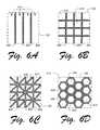
- FIG. 6Ais a plan view of an exemplary intracavity structure of the present invention showing an array of substantially parallel rectanguloid elements.
- FIG. 6Bis a plan view of an exemplary intracavity structure of the present invention showing an array of orthogonally disposed rectanguloid elements.
- FIG. 6Cis a plan view of an exemplary intracavity structure of the present invention showing rectanguloid elements disposed so as to create substantially trianguloid subcavities.
- FIG. 6Dis a plan view of an exemplary intracavity structure of the present invention showing a hexagonal elements disposed within a substantially rectanguloid cavity.
- FIG. 6Eis a plan view of an exemplary intracavity structure of the present invention showing an array of substantially parallel rectanguloid elements disposed within a substantially cylindrical cavity.
- FIG. 6Fis a plan view of an exemplary intracavity structure of the present invention showing an array of torrodial or cylindrical elements disposed within a substantially cylindrical cavity.
- FIG. 7is a cross-sectional view of a substrate of the present invention showing a coating with a barrier layer and/or seed layer.
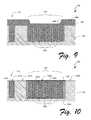
- FIG. 8is a cross-sectional view of a substrate of the present invention showing a conductive material deposited on the barrier and/or seed layer on the substrate.
- FIG. 9is a cross-sectional view of a substrate of the present invention showing additional conductive material completely filling a large cavity.
- FIG. 10is a cross-sectional view of a substrate of the present invention illustrating a depiction of the substrate after a structure is polished.
- FIG. 11illustrates a cross-sectional view of a substrate of the present invention where conductive material that was deposited over an intracavity structure is selectively coated by a suitable barrier material.
- FIG. 12shows a cross-sectional view of a substrate of the present invention where a thin layer of a material is selectively deposited over a conductive material that fills a via or cavity.
- FIG. 13illustrates a cross-sectional view of a substrate of the present invention with a bottomless cavity or via, and an intracavity structure being inserted into the cavity or via from the bottom of the substrate.
- FIG. 14illustrates a cross-sectional view of a substrate of the present invention with a bottomless cavity or via, where an intracavity structure is positioned in the cavity or via from the bottom of the substrate.
- FIG. 15shows a cross-sectional view of a substrate of the present invention with a bottomless cavity or via, where a conductive material had been deposited in the cavity or via, and the intracavity structure is partially withdrawn.
- FIG. 16shows a cross-sectional view of a substrate of the present invention with a bottomless cavity or via, where a conductive material had been deposited in the cavity or via, and the intracavity structure is withdrawn.
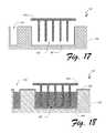
- FIG. 17shows a cross-sectional view of a substrate of the present invention, where an intracavity structure has been positioned within at least part of a cavity or via of the substrate.
- FIG. 18shows a cross-sectional view of a substrate of the present invention, where an intracavity structure has been positioned within at least part of a cavity or via of the substrate, and a conductive material deposited as to partially or substantially fill vias and cavities within the substrate.
- FIG. 19shows a cross-sectional view of a substrate of the present invention, where an intracavity structure is being withdrawn from a partially or substantially filled cavity or via.
- FIG. 20illustrates a cross-sectional view of a substrate of the present invention, where an intracavity structure has been withdrawn from a partially filled cavity or via, and then subsequent deposition of conductive material filling the remainder of cavities and vias in the substrate.
- FIG. 21illustrates a cross-sectional view of a substrate of the present invention, where the overburden above a top surface of the substrate has been removed, forming a planar or substantially planar surface with respect to the top surface of the substrate.
- FIG. 22is a perspective view of a portion of an electronic assembly of the present invention illustrating a preformed intracavity structure being placed within a cavity or via in the substrate from a top opening of the cavity or via.
- FIG. 23is a perspective view of a portion of an electronic assembly of the present invention illustrating a preformed intracavity structure being placed within a cavity or via in the substrate from a bottom opening of the cavity or via.
- a semiconductor substratesuch as a chip or wafer
- a method or apparatus consistent with the present inventionmay be implemented with any assembly, flexible or rigid, that can be energized to convey electrical signals, including but not by way of limitation, wafers, flat panels, magnetic film heads, integrated circuits, electronic devices, semiconducting chips, and packaging substrates.
- aspects of the present inventionmay be employed with any process for manufacturing integrated circuits, substrates, electronic assemblies, or printed wiring boards that currently exists or is later developed, as long as such processes are capable of depositing and removing elements of a conductive interconnect structure within a cavity in a substrate.
- Embodiments of the present inventionaddress the problems encountered in depositing conductive materials on substrates with deep cavities, especially where the opening dimension of the cavities vary greatly.
- the dimensions of the cavitiesare such that the large cavities on the substrate may be only filled by conformal electrodeposition process.
- the present inventiondiscloses a structure and process that improves device yield and throughput.
- One embodiment of a method of the present inventionincludes placing one or more intracavity structures within a cavity prior to deposition of a conductive material.
- elements of the intracavity structure 400are shown within a large cavity 120 in a partial view of a substrate 130 .
- the substratemay be part of a semiconductor integrated circuit or other electronic assembly 100 .
- the smaller via or cavity 110may or may not include a similar structure to the illustrated intracavity structure 400 , although those of skill in the art that any number of cavities within a substrate 130 may include such structures.
- the intracavity structure 400is placed in the cavity 120 by fabrication.
- the intracavity structure 400may be fabricated by use of one or more conventional lithographic steps and etching processes to create a recessed substructure within large cavities in the substrate.
- the material comprising the structuremay include conductors such as copper, aluminum, nickel, tungsten, silver, gold, or suitable alloys, or may comprise nonconductors including aluminum oxide, epoxy-based or non-epoxy based resins.
- an expendable intracavity structure 400may comprise one or more high temperature waxes or other materials that could be readily dissolved in a suitable solvent.
- the expendable intracavity structuremay be pre-formed and placed within the via or cavity 120 , or fluidly deposited in the via or cavity 120 by patterning, extrusion, adhesion, or any appropriate technique, and such fluidly deposited expendable intracavity structure may form a desired shape comprising subcavities.
- the expendable intracavity structure 400may be dissolved or otherwise removed after the via or cavity 120 has been partially plated, and then the plating process continued until a desired amount of fill has been achieved within the via or cavity 120 .
- the intracavity structure 400may also be partially or completely pre-fabricated outside of the cavity.
- the intracavity structure 400may be prefabricated by conventional means including, but not limited to such manufacturing techniques as lithography, RIE, forging, stamping, casting, welding, or other automated fabrication process.
- FIG. 4Bthe prefabricated intracavity structure 400 is shown being inserted into the cavity or via 120 , the prefabricated intracavity structure 400 being dimensioned to fit within the volume defined by the cavity 120 .
- the structure 400may be inserted into the cavity, and aligned within the cavity by any conventional means such as optical, mechanical, electronic, or any other alignment means.
- the intracavity structure 400may be adhered to one or more of the sidewalls 123 , and if the cavity 120 has a defined bottom 124 as shown in FIG. 4B , the intracavity structure 400 may be adhered to the bottom 124 of the cavity 120 .
- the intracavity structure 400may be sized so as to be set back from each of the sidewalls 123 and adhered to the bottom 124 of the via or cavity 120 . Adhesion may be accomplished through a pressure/friction fit, an ultrasonic weld, surface tension, or an adhesive, or may be simply retained by gravity until a further deposition step secures the structure within the cavity.
- intracavity structure 400is fabricated within the cavity 120 or prefabricated and inserted into the cavity 120 , those of skill in the art appreciate that elements of the intracavity structure 400 may abut the walls 123 of the cavity 120 , or may be physically disjoint from connection with the cavity walls 123 . Those of skill in the art also appreciate that while the elements of the intracavity structure 400 are generally shown as rectangularly shaped in cross section, different cross-sectional profiles may result from the manufacturing or deposition process that creates the elements of the intracavity structure 400 , including both linear, trapezoidal, and curvilinear profiles.
- the structure 400may be fabricated from silicon wafer by lithographic and RIE techniques.
- the patterned silicon substratemay then be oxidized to form SiO 2 layer over its surfaces.
- selected plating substancessuch as copper will not adhere to the SiO 2 but will adhere to conductive silicon.
- Similar approachesmay be used on an intracavity structure 400 that is intended to be removed from a cavity or via 120 after the via or cavity is partially or fully filled (see, e.g., FIGS. 13-19 ).
- intracavity structure 400different embodiments of intracavity structure 400 are shown from a plan view in relation to embodiments of a cavity or via 120 .
- the elements of the intracavity structure 400may or may not come into contact with sidewalls (not shown) of the cavity 120 .
- Elements of the intracavity structure 400may consist of curvilinear and non-curvilinear geometrical elements or combination of both.
- the geometrical elements of the intracavity structure 400wholly or partially partition the volume of the cavity into subcavities 410 .
- Embodiments of the intracavity structure 400may comprise elongate elements that do not touchingly engage one another ( FIG.
- FIGS. 6E and 6Fshow cylinder-shaped vias or cavities 120 from a plan view, and elements of intracavity structures 400 in a non-curvilinear arrangement ( FIG. 6E ) and a curvilinear arrangement ( FIG. 6F ).
- the intracavity spaceis wholly or partially partitioned into subcavities 410 .
- Those of skill in the artshould recognize that other shapes may be used, and that combinations of shapes of elements may be utilized in varying embodiments of the present invention.
- a cross section of the substrate 130is shown, where the cross section was taken along a witness line extended between points B and B′ in FIG. 4A .
- FIGS. 5 and 7 - 12also show similar cross sectional depictions.
- a horizontal dimension of a subcavity 410is defined by the geometry and placement of elements of a intracavity structure 400 , and may range, for example, between 5 to 20 microns, and in one embodiment, the thickness 420 of each element of an intracavity structure 400 is smaller than the distance or width 430 between adjacent elements of the intracavity structure 400 .
- the thickness 420 of each element of an intracavity structure 400may vary, and may be selected to comprise suitable dimensions to ensure even and efficient fill of a subcavity 410 .
- the thickness 420 of each element of an intracavity structure 400may exceed the distance 430 between adjacent elements of the intracavity structure 400 .
- the placement of elements in the intracavity structure 400is selected to create a subcavity width 430 that is substantially the same width as a smaller via 110 . In one embodiment illustrated in FIG.
- elements of the intracavity structure 400are reduced in height by a predetermined amount 510 so that the reduced height 522 of the intracavity structure 400 is less than the depth 122 of the via or cavity 120 .
- elements of the intracavity structureare reduced in height by less than 50% of their originally fabricated height.
- elements of the intracavity structureare reduced in height by a predetermined amount 510 that is equal to the final deposited thickness of the conductive substance (see, e.g., 800 , FIG. 9 ). Height adjustment of the intracavity structure 400 may be followed by appropriate cleaning steps to remove residues.
- pre-fabricated intracavity structures 400may also be fabricated to any desired height such as a height equal to or less than the depth 122 of the via or cavity 120 with or without a separate height reduction step.
- the substrate 130is coated with a suitable barrier layer and/or seed layer 700 before deposition of a conductive material.
- the barrier and/or seed layer 700also conformally coats the interior spaces of the via or cavity 120 as well as the intracavity structure 400 .
- a conductive material 800is shown deposited on the barrier and/or seed layer 700 on the substrate 130 , coating and at least partially filling the cavities 110 , 120 , and subcavities 410 .
- the deposition processincludes coating with a conductive material such as a metal using a plating bath containing superfilling additives and an adequate plating process to produce void-free depositions in the small cavity 110 .
- the partitioned large cavity 120 with the recessed intracavity structure 400is thus substantially filled while the small cavity 110 is filled.
- FIG. 8shows when compared to prior art FIG. 2 , processes of the present invention produce a dramatic decrease in the amount of conductive material deposited in a single step without buildup of a substantial overburden, minimizing material and process costs.
- an overburden 940is created that is substantially smaller than the overburden resulting from prior art processes shown in FIG. 3 ( 240 ).
- the smaller total overburden and overburden rangegreatly improves the throughput of any subsequent metal removal steps in the present invention.
- various materialsmay be used as the conductive material 800 to fill cavities or vias 110 , 120 .
- These materialsinclude, but are not limited to copper, nickel, tungsten, silver, aluminum or suitable metal or alloys.
- conductive materialsthose of ordinary skill in the arts appreciate that other substances, including nonconductive substances, may be used in a similar manner to completely or partially fill cavities or vias 110 , 120 to achieve a desired result.
- partitioning the large cavities 120 into subcavities 410dramatically reduces the conductive material coating times from more than 120 minutes to less than 20 minutes. Further, methods of the present invention produce a dramatic reduction in conductive material overburden 940 from more than 50 ⁇ m for prior art approaches to less than 5 ⁇ m in certain implementations. The smaller overburden or other undesired substances may be easily removed by conventional processes such as CMP or eCMP methods.
- the polished structure within the dashed box 1000includes conductive material-filled subcavities, separated by a now integrated intracavity structure 400 .
- the volume above 1022 the integrated intracavity structure 400is filled with a contiguous conductive material 800 .
- the intracavity structure 400acts as a stiffening member, especially in alternate implementations where the sidewalls are coated with high modulus barrier materials such as Ta, TaN, TaN/Ta, and WCN.
- the top surface 1020 of the polished structure 1000forms a substantially planar surface with the polished top 1030 of the substrate 130 , and the polished top 1010 of the smaller cavity or via 110 .
- the deposited conductive material 800may also be bonded to other structures.
- the metal overburdenmay be reduced to less than 20 ⁇ m. Reducing or polishing a thick metal overburden is expensive and time consuming. In certain embodiments it is possible to remove most of the excess conductive material by a high precision, low force, high speed, and high throughput milling machine using a polyether phosphate solution as lubricant and a metal passivating agent. After the conductive material milling step is completed, any remaining unwanted metal or conductive material is removed by a conventional eCMP or CMP method.
- the conductive material 800 deposited over the intracavity structure 400may be selectively coated with a suitable barrier material 1110 .
- a suitable barrier material 1110For example, but not by way of limitation, CoWP and NiP may be deposited over the contiguous conductive material 800 by a method such as an electroless plating method.
- the barrier material 1110(such as NiP or CoWP) is preferably coated with gold by electroless methods to form a bonding layer 1120 .
- Several desirable gold coated surfacescan be aligned and bonded at low temperatures.
- other barrier layers 1110 or films using materialssuch as CoBP and CoWP may be applied over the contiguous conductive material region of the filled via or cavity 120 .
- a thin layer 1220(for example, but not by way of limitation, from 10 nm to 5000 nm in thickness) of a material such as indium may be selectively deposited over the conductive material 800 that fills the via or cavity 120 .
- the indium layer 1220may be used as a bonding layer at temperatures below 400 degrees Celsius.
- the reduction/recess stepsmay be conducted before the thin layer 1220 is deposited on the conductive material 800 . This embodiment creates a new surface 1210 that causes any bond pads formed on the layer 1220 to be elevated above the substrate surface 1210 .
- the intracavity structures 400 of the present inventionprovide structural strength in the finished conductive element that results from filling the via or cavity 120 with a conductive material. Such strength may be desired when, for example, a bonding pad is to be fabricated on a surface of the filled via or cavity, and a significant mechanical force is required to be applied to the surface of the filled via or cavity to bond a device such as a bond wire to the bonding pad.
- the externally fabricated structure 400may be inserted into the large cavities or vias 120 in the substrate 130 .
- the conductive materialis then plated substantially onto the substrate.
- the deposition stepis momentarily stopped then the fabricated structure 400 is carefully removed.
- the substratemay be rinsed briefly to remove any residues or particulates before plating to complete the filling of the features of interest, such as a via or cavity 120 .
- alternative embodimentsallow from insertion of the pre-formed intracavity structure into either the top of the via or cavity 120 , or through the bottom of a bottomless via or cavity 120 .
- a via or cavity 120may be formed in the substrate 130 without a bottom.
- An intracavity structure 400is inserted to the via or cavity 120 through a bottom side of the substrate 130 .
- the intracavity structure 400may be insertable and removable, and may be reusable, dissolvable, or disposable.
- the intracavity structure 400may comprise any suitable shape to allow definition of subcavities within the via or cavity 120 , and the relative thickness (see, e.g., 420 in regards to FIG. 4C ) of the tines 1300 shown on the intracavity structure 400 may vary depending on desired fill rates of subcavity volumes.
- FIGS. 13-21are shown in cross section, the view of the intracavity structure 400 is also shown in cross section. While the tines 1300 are shown in rectilinear shape in FIGS. 13 and 23 , those of skill in the art appreciate that the tines may comprise any suitable cross section, including a trapezoidal cross section with the broad end of the trapezoid adjacent to the base 1310 of the intracavity structure 400 , whereby extraction of the intracavity structure 400 from a deposited conductive material may be facilitated.
- the intracavity structure 400is fully inserted into the via or cavity 120 , and in the illustrated embodiment, by approximating a bottom surface 1400 of the substrate 130 , a surface of the intracavity structure defines a temporary bottom 1410 for the via or cavity 120 , and similarly to the approach discussed in regards to FIG. 4C , the via or cavity 120 is thereby fully or partially partitioned into a plurality of subcavities 410 . As discussed in regards to FIGS. 7-9 , the via or cavity 120 may be partially or completely filled with a conductive material 800 . FIG.
- FIG. 15shows the via or cavity 120 coated with barrier/seed layer 700 and filled with conductive deposition material 800 , and the intracavity structure 400 being withdrawn, (or alternatively, dissolved or otherwise removed) from the filled via or cavity 120 .
- the intracavity structure 400is shown fully withdrawn in FIG. 16 , leaving defined voids 1600 within the filled cavity or via 120 .
- the voids 1600may be left in place, or in one embodiment, additional conductive or nonconductive deposition material may then be deposited on the bottom side 1400 of the substrate 130 to fill the voids 1600 , and if desired, additional planarization steps may be undertaken to remove any overburden from the bottom side 1400 of the substrate 130 .
- the pre-formed intracavity structure 400is partially or completely inserted into a via or cavity 120 in the substrate 130 , the via or cavity 120 having a bottom 124 .
- the substrate 130is optionally coated with a suitable barrier layer and/or seed layer 700 before deposition of a conductive material 800 , and conductive material 800 is deposited, partially filling the via 110 and the via or cavity 120 .
- additional conductive material creating an overburdenmay be deposited on exposed surfaces such as the top surface of the substrate 130 , but for purposes of clarity, such overburden is omitted from FIGS. 18 and 19 .
- the amount of conductive material 800 initially depositedmay slightly fill, partially fill, substantially fill, completely fill, or overfill the via 110 and via or cavity 120 .
- FIG. 19shows the intracavity structure 400 being withdrawn (or alternatively dissolved or otherwise removed) from the partially filled via or cavity 120 , leaving behind voids 1900 in the conductive material.
- additional conductive material 800is deposited, completely filling the via 110 , the via or cavity 120 , and the voids 1900 (the now-filled voids 2010 and the prior fill level 2000 are shown for comparative purposes in dashed lines).
- the structure 400may be selectively removed or dissolved through application of a suitable solvent or other removal process.
- a planarization processmay be implemented to remove the deposited overburden 2020 , and produce a substantially planar top surface 2100 of the substrate 130 .
- an electrically reactive componentmay be formed within a cavity or via 120 .
- the walls of the subcavitymay be coated with a conformal insulator.
- the insulatormay be coated by a suitable metal such as platinum, rhodium. WCN, or alpha-Ta (i.e. the low resistivity crystalline phase of Tantalum).
- the remaining gapis the filled with a suitable insulator, preferably a high dielectric constant insulator.
- the substrateis planarized to form a high performance capacitor.
- Such device structuremay find applications in such practices as high precision timing elements.
- methods of the present inventionmay be utilized to deposit traces or signal lines with embedded void areas that have purposely been left unfilled, or filled with a nonconductor or dielectric.
- traces or signal lines with embedded void areasthat have purposely been left unfilled, or filled with a nonconductor or dielectric.
- Those of skill in the relevant artsappreciate that high frequency signals tend to travel toward the surface of a conductor, and the higher the frequency, the less the signal penetrates into the cross section of the conductor (also known as the “skin effect”). This effect allows high frequency signals to propagate through these void-embedded or dielectric-filled signal lines substantially unimpeded. Further, this use of intentionally fabricated voids or dielectric-filled trace or signal lines may also be desirable to obtain a desired characteristic impedance of the trace or signal lines, where higher frequency signals may effectively propagate, while lower frequency signals are selectively impeded.
- Embodiments of such void-containing traces or signals linesmay also provide for a filtered signal line, such as provided by a passive high-pass filter. Selection of the geometry and aspect of the signal lines with respect to the embedded voids or dielectric fills provides for flexibility of selecting characteristic impedance or transmission line performance.
Landscapes
- Engineering & Computer Science (AREA)
- Microelectronics & Electronic Packaging (AREA)
- Computer Hardware Design (AREA)
- Power Engineering (AREA)
- Physics & Mathematics (AREA)
- Condensed Matter Physics & Semiconductors (AREA)
- General Physics & Mathematics (AREA)
- Manufacturing & Machinery (AREA)
- Internal Circuitry In Semiconductor Integrated Circuit Devices (AREA)
Abstract
Description
1. Field of the Invention
The present invention relates to a method and apparatus for providing electrical interconnects. More specifically, the present invention relates to fabricating connective structures within defined areas of a substrate such as a semiconductor wafer, a semiconductor chip, a multichip module, or a printed wiring assembly. Further, the present invention relates to embodiments of electrically reactive interconnect components.
2. Background of the Invention
Creating electrical interconnections is a challenging and essential part of manufacturing compact electronic components and systems, particularly in the field of manufacturing integrated circuits. Over time, automated methods have been developed to deposit conductive materials on substrates, in layers of substrates, or through cavities such as trenches, holes, and vias of a substrate. Deposition of materials in such cavities provides for electrical interconnections between conductive traces on multiple layers of a substrate, essentially connecting components and terminals in various locations of the substrate to create an integrated circuit or system. More specifically, in typical integrated circuits, multiple levels of interconnect networks extend laterally with respect to the substrate surface. Interconnects formed in parallel substrate interlayers can thus be electrically connected using vias or cavities filled with conductive materials.
In a typical integrated circuit fabrication process, first an insulating interlayer is formed on a semiconductor substrate. Patterning and etching processes (such as those incorporating reactive ion etching (RIE)) are employed to form features such as trenches, vias, and cavities in the insulating layer. Then a conductive material such as copper is deposited to fill the cavities by processes such as sputtering, CVD, electrodeposition, electroless plating, or a combination of those approaches. Once the conductive material is applied, a conventional process such as chemical-mechanical polishing/planarization (CMP) is employed to remove the excess conductive material that was deposited above the top surface of the substrate. This removal results in an essentially flat surface, which is substantially planar with the top surface of the remainder of the substrate. These processes are repeated multiple times to manufacture multi-layer interconnects.
Recently, research has been applied in the semiconductor fields to three-dimensional (3D) wafer- and package-level integration, which is becoming an increasingly important enabling technology for integrated circuits and packages. Three-dimensional integration offers potentials for higher device and package performance, greater interconnectivity and functionality, heterogeneous systems integration, reductions in packaging size and cost, and improvements in device and/or package reliability. One of the proposed approaches to implement 3D interconnection utilizes arrays of vias or cavities, which may vary dramatically in size within the same substrate.
Exemplary embodiments of prior art processes may be explained though review ofFIGS. 1A ,1B,2, and3. Referring toFIG. 1A , asubstrate 130 forms the mechanical support for an electrical interconnect system such as anintegrated circuit 100, which is shown with a smaller via/cavity 110 and a substantially larger via/cavity 120. The illustrated vias orcavities substrate 130, havingsidewalls 123 and abottom 124.FIG. 1B depicts an exemplary cross section of the integratedcircuit substrate 130 shown inFIG. 1A , the cross section being taken through line formed between points A-A′ inFIG. 1A . A conductinglayer 140 is shown conformally coating the vias orcavities top surface 133 of thesubstrate 130, which may include an insulating layer such as SiO2. The conductinglayer 140 often comprises abarrier layer 155, and may also comprise aseed layer 157 which may be deposited on thebarrier layer 155. Depending on the particular process used, the seed layer may range from 20 to 4000 angstroms in thickness. Thebarrier layer 155 coats the insulating layer to ensure good adhesion and acts as a barrier material to prevent diffusion of conductive materials such as copper into the insulating layers and into semiconductor devices fabricated in thesubstrate 130. Theseed layer 157 forms a conductive material base for metal crystal growth such as when copper is used during subsequent metal depositions.
The illustrations inFIG. 1A andFIG. 1B show that some cavities or vias such as the larger via120 may range indiameter 121 from 5 μm to 2000 μm or more. Thedepth 122 of vias orcavities cavities
In prior art systems, providing electrical conductivity through vias orcavities vias substrate 130, it is desirable to overfill the cavities to, for example, 20% to 200% of the via orcavity depth 122 in order to minimize defects in the wiring structure. However, when the dimensions of vias orcavities same substrate 130, the procedures required to consistently and reliably fill cavities of such varying sizes results in an expensive and high-cost production process. For example, with respect toFIG. 2 , for asubstrate 230 containingvias conductive material 250 in 15 minutes by conventional electrocoating methods, while larger cavities such as the illustrated 30 μm and larger via220 are substantially under-filled. To completely fill allvias FIG. 3 , a conductive material250 (such as a copper film) is deposited (such as by electroplating) onto the conductinglayer 140, and theconductive material 250 quickly fills the small via110 but coats the wide via220 and the surface of thesubstrate 230 in a conformal manner. For practical purposes, the metal deposition process may be required to operate for more than two hours to completely fill the 500 μm via220 depicted inFIG. 3 . After thelarger via 220 is filled, asubstantial overburden 240 is also deposited on thesubstrate 230. The maximum thickness of the overburden240 that overlies thetop surface 133 of thesubstrate 230 is related to the depth (FIG. 1B ,122) of the feature with the largest width (FIG. 1B ,121), to be filled on thesubstrate 230, which is in this example the cavity or via220. As cavities or vias are filled, the thickness of overburden varies. For example, the depositedoverburden 240 is thicker above over areas of thesubstrate 230 without vias or cavities, and the overburden240bis thinner above areas such as the wide via orcavity 220. The substantial range of thicknesses in overburden (240,240b) is problematic in many ways, particularly in planarization of the top surface of thesubstrate 230.
The overburden240 must ultimately be removed with a conventional process such as a chemical-mechanical planarization (CMP) procedure, by an electro-chemical mechanical polishing/planarization procedure (eCMP), by a wet etch procedure, or by their various combinations. Polishing to remove such a large range of overburden depths is time consuming and expensive. In an exemplary prior art process, such extensive planarization processes have a throughput of less than one-third wafer per hour. Apart from higher process costs, device yields after such extensive deposition and etching steps may be negatively impacted, resulting in large variations in desirable device parameters. For example, when attempting to remove an overburden with wide ranges of thicknesses (240a,240b), the areas over vias or cavities such as thelarge cavity 220 inFIG. 3 may be subject to dishing, or the excessive removal of material resulting in the creation of a non-planar surface above vias or cavities. What is needed, then, is a process for efficiently filling cavities in a substrate, particularly when cavities in a substrate vary in size with respect to one another. What is also needed is a method for filling vias or cavities within a substrate while minimizing the range thicknesses of overburden deposited above all areas of the substrate. What is also needed is a process and apparatus to form electrically conductive or electrically reactive components within a cavity in a substrate. What is further needed is a method to form bonding pads utilizing conductive structures within cavities or vias.
Terminology
The terms, chip, integrated circuit, monolithic device, semiconductor device or component, microelectronic device or component, and similar terms and expressions, are often used interchangeably in this field. The present invention is applicable to all the above as they are generally understood in the field, as well as to printed circuit boards, printed wiring boards, and printed wiring assemblies, also which may be used interchangeably.
The terms metal line, trace, wire, conductor, signal path and signaling medium are all related. These terms are generally interchangeable, and appear in order from specific to general. In this field, metal lines are sometimes referred to as traces, wires, lines, interconnects, conductive materials, or simply metal. The term vertical, as used herein, means substantially perpendicular to the major surface of a substrate. The term horizontal, as used herein, means substantially parallel to the major surface of a substrate.
The terms “cavity” and “via” both refer to structures providing electrical connection of conductors from different interconnect levels within a substrate, or from within a substrate to a next higher level assembly. Vias and trenches are forms of cavities typically used to provide for interconnection within a device. Cavities that are filled to provide electrical connections between a plurality of levels may be considered vias. Cavities that are filled to provide electrical connections within the same level may be referred to as trenches. These terms are sometimes used in the art to describe both an opening in an insulator in which the structure will be completed, and the completed structure itself.
As used herein, the term “filled” also means “substantially filled.”
Summary
The present invention discloses methods for depositing a material, particularly a conductive material, in cavities of a substrate and forming bonding contacts or pads thereon. Also provided are embodiments for interconnection structures using filled cavities, along with electrically reactive structures which may include capacitors fabricated within a substrate.
One embodiment includes a method for filling a cavity defined within a substrate, where the cavity has sidewalls, and optionally, a bottom. The method involves placing an intracavity structure within the cavity, the intracavity structure partitioning the cavity into a plurality of subcavities and substantially filling the subcavities with a conductive deposition material. As defined herein, partitioning may include a partial partitioning, that is, partitioning the cavity into subcavities that remain partially connected within the volume defined within the cavity. The intracavity structure may be fabricated outside the cavity and then placed within the cavity, or the intracavity structure may be fabricated within the cavity, by processes such as photolithography and etching.
The intracavity structure may comprise any suitable shape. In exemplary embodiments, structural elements of the intracavity structure may include an array of shaped elements such as hexagonal elements, conic elements, rectanguloid elements, cubic elements, trianguloid elements, torroidial elements, rhomboid elements, and combinations of those elements. In an alternate embodiment, the intracavity structure may comprise a plurality of elements that do not interconnect with one another, but provide structural support to the sidewalls and/or the bottom of a cavity or via. In another embodiment, the shaped elements of the intracavity structure, when aligned, form a substantially planar arrangement. In another embodiment, once the intracavity structure is placed within the cavity, at least part of the intracavity structure is reduced through a process such as etching, bringing the vertical dimension of the intracavity structure to an amount less than a predetermined vertical dimension of the sidewalls of the cavity.
In one embodiment, a barrier layer may be deposited on at least part of the intracavity structure, the bottom surface of the cavity, and/or the sidewalls of the cavity, for example, after the intracavity structure has been placed within the cavity. The barrier layer may be used to coat the sidewalls and/or bottom of the cavity to ensure good adhesion of further fill materials, and may act as a barrier material to prevent diffusion of conductive fill materials such as copper into the elements of the substrate such as insulating layers and semiconductor devices. The barrier layer may comprise any appropriate material, such as Ta, TaN, WCN, TiN, WN, TbN, VN, ZrN, CrN, WC, WN, NbN, AlN, or combinations of those materials.
In another embodiment, a seed layer may be deposited within at least a portion of the cavity. The seed layer forms a base for growth of a conductive material such as crystalline copper during subsequent conductive material deposition steps. In an alternate implementation, a second conductive layer may be deposited on the first layer of conductive deposition material in an amount sufficient to fill the cavity and create an overfilled volume above the tops of the cavity sidewalls. At least part of the second conductive layer may be removed to form a substantially planar surface with a top surface of the substrate by processes such as a CMP process, an eCMP process, or a milling process and other various combinations of these processes. The conductive material and the second conductive layer material deposited in the cavity, the subcavities, or on the substrate may comprise Cu, Ni, W, Au, Ag, Al, along with their alloys and other combinations of conductive materials.
In one implementation, a bonding layer, a barrier layer, or a combination of the two may be deposited on at least a portion of the surface of the planarized second conductive layer material. The barrier layer material may be any appropriate material such as CoP, NiP, CoBP, CoWP, along with their alloys and other combinations. The bonding layer may comprise indium, gold, copper, or other appropriate bonding materials.
In an alternate embodiment, functional components such as electrically reactive components may be formed within cavities by methods of the present invention. For example, but not by way of limitation, steps to form a reactive component such as a capacitor include depositing a conformal insulator within the cavity, depositing a conductive electrode layer on the conformal insulator, filling the remaining unoccupied volume of the cavity with a filling insulator; and planarizing the filling insulator to form a substantially planar surface with the substrate. The planarizing may be accomplished by processes such as a CMP process, an eCMP process, or a milling process, and combinations of these processes. The conductive electrode layer may be selected from materials such as Pt, Rh, WCN, and alpha-Ta.
In another implementation, methods of the present invention provide for partitioning the cavity into a plurality of subcavities, each of the subcavities having a respective predetermined subcavity volume. An initial conductive layer is deposited within at least one of the subcavity volumes, where the barrier layer is for electrical communication with a conductive element in the substrate. A conductive material may then be deposited within the plurality of subcavities. In one embodiment, the conductive material substantially fills at least one of the subcavity volumes to a predetermined amount. A second conducive material may be deposited proximate to the cavity defined within the substrate; and part of the second conductive material removed to form a substantially planar surface between the second conductive layer and a surface of the substrate such as the top of the substrate. In alternate embodiments, the predetermined subcavity volume is less than a volume of a second cavity defined within the substrate, where the cavity defined within the substrate and the second cavity are separated by at least part of the substrate.
In another embodiment, there is provided a method for filling a cavity defined within a substrate, the cavity having a bottom and sidewalls. The method includes placing a pre-formed structure within the cavity where the pre-formed structure partitions the cavity into a plurality of subcavities. The preformed structure may comprise any suitable material, but in certain embodiments may form conductive materials such as copper, aluminum, nickel, tungsten, silver, gold, or suitable alloys. The preformed structure may also, in alternate embodiments, comprise memory metals, or other composite substances such as alumina. In certain embodiments, the preformed structure has a predetermined vertical dimension less than a height dimension of the sidewalls and has a predetermined footprint area (e.g, the cross sectional area of a projection through the vertical dimension of the structure) that is less than or equal to an area of the bottom of the cavity. A metal layer is deposited within at least one of the subcavity volumes, where the metal layer is for electrical communication with a conductive element in the substrate such as a via or other conductive trace, and the subcavities are substantially filled with a conductive deposition material.
Another embodiment of the present invention provides for an interconnection feature that has a volume defined within a cavity in a substrate, one or more intracavity structures partitioning the volume into a plurality of subcavities; and a deposited metal layer substantially filling at least one of the plurality of subcavities. In one implementation, at least a portion of the deposited metal layer is for electrical communication with a conductive element of the substrate, such as a metal trace, a terminal of a component, or a via.
Embodiments of the present invention also provide for a substrate having electrically reactive component, such as a capacitor. The substrate, in one implementation, includes a cavity defined within the substrate, the cavity having a bottom and sidewalls. The substrate also has one or more intracavity structures residing within the cavity that partition the cavity into a plurality of subcavities, a conformal insulator coating the one or more intracavity structures, and a conductive electrode layer deposited within the cavity and in proximity to the conformal insulator. Embodiments further include a high-dielectric constant insulator deposited within the cavity and in communication with the conductive electrode layer, where the high-dielectric constant insulator substantially fills the volume in the cavity that is not occupied by the intracavity structures, the conformal insulator, and conductive electrode layer and forms a substantially planar surface with the substrate. Such an electrically reactive component may be fabricated in a variety of shapes and sizes, using geometries and materials (such as the choice of the high dielectric constant insulator) that are selected to achieve a desired electrical performance characteristic such as capacitance. In one embodiment, the substrate includes a cavity defined within the substrate, the cavity having sidewalls but no bottom and no top. In this embodiment, an intracavity structure may be inserted to begin the plating or deposition process, and at some point during the plating process, the intracavity structure may be removed from either the top or the bottom of the cavity, and once removed, plating process may be continued until the cavity has been filled to a desired amount. Removal of the intracavity structure may be by any appropriate means, such as mechanical force, chemical etching, RIE processes, or other techniques.
In another embodiment, there is provided a method for filling a cavity defined within a substrate, the cavity having sidewalls, including the steps of placing a pre-formed structure within the cavity, the pre-formed structure partitioning the cavity into a plurality of subcavities; depositing a metal layer within at least one of the subcavity volumes, wherein the metal layer is for electrical communication with a conductive element in the substrate; and substantially filling the subcavities with a conductive deposition material. In one implementation, the cavity further includes a bottom; and the pre-formed structure comprises a conductive material, has a predetermined vertical dimension less than a height dimension of the sidewalls, and has a predetermined footprint area less than or equal to an area of the bottom of the cavity. In an embodiment, the pre-formed structure comprises a non-conductive material; and has a predetermined footprint area less than or equal to an area of the bottom of the cavity. The pre-formed structure may reside entirely within, inside, or partially outside the via or cavity during application of a conductive material to the substrate, and after subcavities in the via or cavity are at least partially filled with a conductive deposition material, the pre-formed structure may be removed from the cavity and the substrate. Then a second conductive layer may be deposited on the previously deposited the conductive deposition material, the second conductive layer deposited in an amount sufficient to fill the cavity and create an overfill above a top surface of the substrate. At least a portion of the second conductive layer may then be removed to form a substantially planar surface including at least the second conductive layer and the substrate. In another embodiment, a second conductive layer may be deposited on a bottom surface of the substrate, the second conductive layer deposited in an amount sufficient to fill voids within the conductive deposition material; and then at least a portion of the second conductive layer may be removed to form a substantially planar surface on the bottom surface of the substrate. Further, an amount of conductive deposition material sufficient to fill the cavity and create an overfill above a top surface of the substrate may be deposited on a top side of the substrate; and at least a portion of the conductive deposition material may be removed to form a substantially planar surface including at least the conductive deposition material and a top surface of the substrate.
The accompanying drawings, which are incorporated in and constitute a part of this specification, illustrate several embodiments of the invention and together with the description, serve to explain the principles of the invention.
It is to be understood that both the foregoing general description and the following detailed description are exemplary and explanatory only and are not restrictive of the invention, as claimed.
Introduction
While systems and methods consistent with the present invention are implemented using a semiconductor substrate such as a chip or wafer, at least as described below with reference toFIG. 4A , those skilled in the art understand that embodiments consistent with the present invention may be employed more generally. For example, a method or apparatus consistent with the present invention may be implemented with any assembly, flexible or rigid, that can be energized to convey electrical signals, including but not by way of limitation, wafers, flat panels, magnetic film heads, integrated circuits, electronic devices, semiconducting chips, and packaging substrates. While vias, cavities, voids, and volumes described herein are shown in the drawings generally with rectanguloid or cylindrical shapes, those of skill in the art appreciate that any shape that is suitable to retain an electrical interconnect within a substrate may be used to implement aspects of the present invention. Additionally, aspects of the present invention may be employed with any process for manufacturing integrated circuits, substrates, electronic assemblies, or printed wiring boards that currently exists or is later developed, as long as such processes are capable of depositing and removing elements of a conductive interconnect structure within a cavity in a substrate.
Description
Reference will now be made in detail to the present exemplary embodiments of the invention, examples of which are illustrated in the accompanying drawings.
Embodiments of the present invention address the problems encountered in depositing conductive materials on substrates with deep cavities, especially where the opening dimension of the cavities vary greatly. In some implementations, the dimensions of the cavities are such that the large cavities on the substrate may be only filled by conformal electrodeposition process. The present invention discloses a structure and process that improves device yield and throughput.
One embodiment of a method of the present invention includes placing one or more intracavity structures within a cavity prior to deposition of a conductive material. With reference toFIG. 4A , elements of theintracavity structure 400 are shown within alarge cavity 120 in a partial view of asubstrate 130. The substrate may be part of a semiconductor integrated circuit or otherelectronic assembly 100. The smaller via orcavity 110 may or may not include a similar structure to the illustratedintracavity structure 400, although those of skill in the art that any number of cavities within asubstrate 130 may include such structures.
In one embodiment, theintracavity structure 400 is placed in thecavity 120 by fabrication. Theintracavity structure 400 may be fabricated by use of one or more conventional lithographic steps and etching processes to create a recessed substructure within large cavities in the substrate. The material comprising the structure may include conductors such as copper, aluminum, nickel, tungsten, silver, gold, or suitable alloys, or may comprise nonconductors including aluminum oxide, epoxy-based or non-epoxy based resins. In another embodiment, anexpendable intracavity structure 400 may comprise one or more high temperature waxes or other materials that could be readily dissolved in a suitable solvent. The expendable intracavity structure may be pre-formed and placed within the via orcavity 120, or fluidly deposited in the via orcavity 120 by patterning, extrusion, adhesion, or any appropriate technique, and such fluidly deposited expendable intracavity structure may form a desired shape comprising subcavities. In this embodiment, theexpendable intracavity structure 400 may be dissolved or otherwise removed after the via orcavity 120 has been partially plated, and then the plating process continued until a desired amount of fill has been achieved within the via orcavity 120.
Theintracavity structure 400 may also be partially or completely pre-fabricated outside of the cavity. Theintracavity structure 400 may be prefabricated by conventional means including, but not limited to such manufacturing techniques as lithography, RIE, forging, stamping, casting, welding, or other automated fabrication process. Referring toFIG. 4B , the prefabricatedintracavity structure 400 is shown being inserted into the cavity or via120, the prefabricatedintracavity structure 400 being dimensioned to fit within the volume defined by thecavity 120. Thestructure 400 may be inserted into the cavity, and aligned within the cavity by any conventional means such as optical, mechanical, electronic, or any other alignment means. Once inserted, theintracavity structure 400 may be adhered to one or more of thesidewalls 123, and if thecavity 120 has a definedbottom 124 as shown inFIG. 4B , theintracavity structure 400 may be adhered to thebottom 124 of thecavity 120. Alternatively, theintracavity structure 400 may be sized so as to be set back from each of thesidewalls 123 and adhered to thebottom 124 of the via orcavity 120. Adhesion may be accomplished through a pressure/friction fit, an ultrasonic weld, surface tension, or an adhesive, or may be simply retained by gravity until a further deposition step secures the structure within the cavity. Whether theintracavity structure 400 is fabricated within thecavity 120 or prefabricated and inserted into thecavity 120, those of skill in the art appreciate that elements of theintracavity structure 400 may abut thewalls 123 of thecavity 120, or may be physically disjoint from connection with thecavity walls 123. Those of skill in the art also appreciate that while the elements of theintracavity structure 400 are generally shown as rectangularly shaped in cross section, different cross-sectional profiles may result from the manufacturing or deposition process that creates the elements of theintracavity structure 400, including both linear, trapezoidal, and curvilinear profiles.
Thestructure 400 may be fabricated from silicon wafer by lithographic and RIE techniques. The patterned silicon substrate may then be oxidized to form SiO2layer over its surfaces. Using this approach, selected plating substances such as copper will not adhere to the SiO2but will adhere to conductive silicon. Similar approaches may be used on anintracavity structure 400 that is intended to be removed from a cavity or via120 after the via or cavity is partially or fully filled (see, e.g.,FIGS. 13-19 ).
Referring toFIGS. 6A-6E , different embodiments ofintracavity structure 400 are shown from a plan view in relation to embodiments of a cavity or via120. As mentioned above, the elements of theintracavity structure 400 may or may not come into contact with sidewalls (not shown) of thecavity 120. Elements of theintracavity structure 400 may consist of curvilinear and non-curvilinear geometrical elements or combination of both. When placed within a via or cavity, the geometrical elements of theintracavity structure 400 wholly or partially partition the volume of the cavity intosubcavities 410. Embodiments of theintracavity structure 400 may comprise elongate elements that do not touchingly engage one another (FIG. 6A ); formations of elements that intersect in a substantially orthogonal manner (FIG. 6B ), arrays of elements that are disposed to form triangularly-arranged subcavities (FIG. 6C ,410), and arrays of elements that are disposed to form an array of heaxgonoid-bounded subcavities (FIG. 6D ,410). As mentioned elsewhere herein, embodiments of the present invention do not limit vias or cavities to rectanguloid shapes. For example,FIGS. 6E and 6F show cylinder-shaped vias orcavities 120 from a plan view, and elements ofintracavity structures 400 in a non-curvilinear arrangement (FIG. 6E ) and a curvilinear arrangement (FIG. 6F ). In each embodiment, the intracavity space is wholly or partially partitioned intosubcavities 410. Those of skill in the art should recognize that other shapes may be used, and that combinations of shapes of elements may be utilized in varying embodiments of the present invention.
With reference toFIG. 4C , a cross section of thesubstrate 130 is shown, where the cross section was taken along a witness line extended between points B and B′ inFIG. 4A . FIGS.5 and7-12 also show similar cross sectional depictions. In an exemplary embodiment, a horizontal dimension of asubcavity 410 is defined by the geometry and placement of elements of aintracavity structure 400, and may range, for example, between 5 to 20 microns, and in one embodiment, thethickness 420 of each element of anintracavity structure 400 is smaller than the distance orwidth 430 between adjacent elements of theintracavity structure 400. Alternatively, thethickness 420 of each element of anintracavity structure 400 may vary, and may be selected to comprise suitable dimensions to ensure even and efficient fill of asubcavity 410. For example but not by way of limitation, in one embodiment thethickness 420 of each element of anintracavity structure 400 may exceed thedistance 430 between adjacent elements of theintracavity structure 400. In another embodiment, the placement of elements in theintracavity structure 400 is selected to create asubcavity width 430 that is substantially the same width as a smaller via110. In one embodiment illustrated inFIG. 5 , elements of theintracavity structure 400 are reduced in height by apredetermined amount 510 so that the reducedheight 522 of theintracavity structure 400 is less than thedepth 122 of the via orcavity 120. In one embodiment, elements of the intracavity structure are reduced in height by less than 50% of their originally fabricated height. In another embodiment, elements of the intracavity structure are reduced in height by apredetermined amount 510 that is equal to the final deposited thickness of the conductive substance (see, e.g.,800,FIG. 9 ). Height adjustment of theintracavity structure 400 may be followed by appropriate cleaning steps to remove residues. Those of skill in the relevant arts should appreciate that pre-fabricatedintracavity structures 400 may also be fabricated to any desired height such as a height equal to or less than thedepth 122 of the via orcavity 120 with or without a separate height reduction step.
As shown inFIG. 7 after theintracavity structure 400 is formed or deposited within the cavity or via120, in one embodiment thesubstrate 130 is coated with a suitable barrier layer and/orseed layer 700 before deposition of a conductive material. The barrier and/orseed layer 700 also conformally coats the interior spaces of the via orcavity 120 as well as theintracavity structure 400.
With reference toFIG. 8 , aconductive material 800 is shown deposited on the barrier and/orseed layer 700 on thesubstrate 130, coating and at least partially filling thecavities subcavities 410. In one embodiment, the deposition process includes coating with a conductive material such as a metal using a plating bath containing superfilling additives and an adequate plating process to produce void-free depositions in thesmall cavity 110. The partitionedlarge cavity 120 with the recessedintracavity structure 400 is thus substantially filled while thesmall cavity 110 is filled. AsFIG. 8 shows when compared to prior artFIG. 2 , processes of the present invention produce a dramatic decrease in the amount of conductive material deposited in a single step without buildup of a substantial overburden, minimizing material and process costs.
With reference toFIG. 9 , when additional conductive material completely fills the large cavity, anoverburden 940 is created that is substantially smaller than the overburden resulting from prior art processes shown inFIG. 3 (240). The smaller total overburden and overburden range greatly improves the throughput of any subsequent metal removal steps in the present invention.
In various embodiments, various materials may be used as theconductive material 800 to fill cavities orvias vias
In certain embodiments, partitioning thelarge cavities 120 intosubcavities 410 dramatically reduces the conductive material coating times from more than 120 minutes to less than 20 minutes. Further, methods of the present invention produce a dramatic reduction inconductive material overburden 940 from more than 50 μm for prior art approaches to less than 5 μm in certain implementations. The smaller overburden or other undesired substances may be easily removed by conventional processes such as CMP or eCMP methods. With reference toFIG. 10 , the polished structure within the dashed box1000 (the dashed box is for illustration purposes only and does not comprise part of the disclosed invention) includes conductive material-filled subcavities, separated by a now integratedintracavity structure 400. In an alternate embodiment, the volume above1022 the integratedintracavity structure 400 is filled with a contiguousconductive material 800. In certain embodiments, theintracavity structure 400 acts as a stiffening member, especially in alternate implementations where the sidewalls are coated with high modulus barrier materials such as Ta, TaN, TaN/Ta, and WCN. Thetop surface 1020 of thepolished structure 1000 forms a substantially planar surface with thepolished top 1030 of thesubstrate 130, and thepolished top 1010 of the smaller cavity or via110. The depositedconductive material 800 may also be bonded to other structures.
For some applications, where the cavity depth (FIG. 5 ,122) may range, for example, from 100 μm to more than 200 μm, by using methods of the present invention, the metal overburden may be reduced to less than 20 μm. Reducing or polishing a thick metal overburden is expensive and time consuming. In certain embodiments it is possible to remove most of the excess conductive material by a high precision, low force, high speed, and high throughput milling machine using a polyether phosphate solution as lubricant and a metal passivating agent. After the conductive material milling step is completed, any remaining unwanted metal or conductive material is removed by a conventional eCMP or CMP method.
With reference toFIG. 11 , in alternate embodiments of this invention, theconductive material 800 deposited over theintracavity structure 400 may be selectively coated with asuitable barrier material 1110. For example, but not by way of limitation, CoWP and NiP may be deposited over the contiguousconductive material 800 by a method such as an electroless plating method. In an alternate embodiment, for bonding applications, the barrier material1110 (such as NiP or CoWP) is preferably coated with gold by electroless methods to form abonding layer 1120. Several desirable gold coated surfaces can be aligned and bonded at low temperatures. In alternate implementations,other barrier layers 1110 or films using materials such as CoBP and CoWP may be applied over the contiguous conductive material region of the filled via orcavity 120.
As shown inFIG. 12 , in another embodiment of this invention, a thin layer1220 (for example, but not by way of limitation, from 10 nm to 5000 nm in thickness) of a material such as indium may be selectively deposited over theconductive material 800 that fills the via orcavity 120. Theindium layer 1220 may be used as a bonding layer at temperatures below 400 degrees Celsius. For improved device yields, in various embodiments it may be preferable to recess or remove portions of thesubstrate 130. This reduction or recess process may be accomplished by a process such as an RIE process followed by a possible cleaning step. In some embodiments, the reduction/recess steps may be conducted before thethin layer 1220 is deposited on theconductive material 800. This embodiment creates anew surface 1210 that causes any bond pads formed on thelayer 1220 to be elevated above thesubstrate surface 1210.
Those of skill in the art also appreciate that theintracavity structures 400 of the present invention provide structural strength in the finished conductive element that results from filling the via orcavity 120 with a conductive material. Such strength may be desired when, for example, a bonding pad is to be fabricated on a surface of the filled via or cavity, and a significant mechanical force is required to be applied to the surface of the filled via or cavity to bond a device such as a bond wire to the bonding pad.
In another embodiment of this invention, the externally fabricatedstructure 400 may be inserted into the large cavities orvias 120 in thesubstrate 130. The conductive material is then plated substantially onto the substrate. The deposition step is momentarily stopped then the fabricatedstructure 400 is carefully removed. The substrate may be rinsed briefly to remove any residues or particulates before plating to complete the filling of the features of interest, such as a via orcavity 120. As discussed in more depth below, alternative embodiments allow from insertion of the pre-formed intracavity structure into either the top of the via orcavity 120, or through the bottom of a bottomless via orcavity 120.
As shown in cross section inFIG. 13 and by perspective inFIG. 23 , a via orcavity 120 may be formed in thesubstrate 130 without a bottom. Anintracavity structure 400 is inserted to the via orcavity 120 through a bottom side of thesubstrate 130. In various embodiments, theintracavity structure 400 may be insertable and removable, and may be reusable, dissolvable, or disposable. Those of skill in the art appreciate that theintracavity structure 400 may comprise any suitable shape to allow definition of subcavities within the via orcavity 120, and the relative thickness (see, e.g.,420 in regards toFIG. 4C ) of thetines 1300 shown on theintracavity structure 400 may vary depending on desired fill rates of subcavity volumes. AsFIGS. 13-21 are shown in cross section, the view of theintracavity structure 400 is also shown in cross section. While thetines 1300 are shown in rectilinear shape inFIGS. 13 and 23 , those of skill in the art appreciate that the tines may comprise any suitable cross section, including a trapezoidal cross section with the broad end of the trapezoid adjacent to thebase 1310 of theintracavity structure 400, whereby extraction of theintracavity structure 400 from a deposited conductive material may be facilitated.
Referring toFIG. 14 , theintracavity structure 400 is fully inserted into the via orcavity 120, and in the illustrated embodiment, by approximating abottom surface 1400 of thesubstrate 130, a surface of the intracavity structure defines atemporary bottom 1410 for the via orcavity 120, and similarly to the approach discussed in regards toFIG. 4C , the via orcavity 120 is thereby fully or partially partitioned into a plurality ofsubcavities 410. As discussed in regards toFIGS. 7-9 , the via orcavity 120 may be partially or completely filled with aconductive material 800.FIG. 15 shows the via orcavity 120 coated with barrier/seed layer 700 and filled withconductive deposition material 800, and theintracavity structure 400 being withdrawn, (or alternatively, dissolved or otherwise removed) from the filled via orcavity 120. Theintracavity structure 400 is shown fully withdrawn inFIG. 16 , leaving definedvoids 1600 within the filled cavity or via120. Those of skill in the art appreciate that thevoids 1600 may be left in place, or in one embodiment, additional conductive or nonconductive deposition material may then be deposited on thebottom side 1400 of thesubstrate 130 to fill thevoids 1600, and if desired, additional planarization steps may be undertaken to remove any overburden from thebottom side 1400 of thesubstrate 130.
In another embodiment shown in cross section inFIG. 17 and by perspective inFIG. 22 , the pre-formedintracavity structure 400 is partially or completely inserted into a via orcavity 120 in thesubstrate 130, the via orcavity 120 having a bottom124. As shown inFIG. 18 , thesubstrate 130 is optionally coated with a suitable barrier layer and/orseed layer 700 before deposition of aconductive material 800, andconductive material 800 is deposited, partially filling the via110 and the via orcavity 120. During this step, additional conductive material creating an overburden may be deposited on exposed surfaces such as the top surface of thesubstrate 130, but for purposes of clarity, such overburden is omitted fromFIGS. 18 and 19 . Those of skill in the art recognize that the amount ofconductive material 800 initially deposited may slightly fill, partially fill, substantially fill, completely fill, or overfill the via110 and via orcavity 120.
In still other embodiments of the present invention, an electrically reactive component may be formed within a cavity or via120. In this embodiment, the walls of the subcavity may be coated with a conformal insulator. The insulator may be coated by a suitable metal such as platinum, rhodium. WCN, or alpha-Ta (i.e. the low resistivity crystalline phase of Tantalum). The remaining gap is the filled with a suitable insulator, preferably a high dielectric constant insulator. After the filling step, the substrate is planarized to form a high performance capacitor. Such device structure may find applications in such practices as high precision timing elements.
In another embodiment, methods of the present invention may be utilized to deposit traces or signal lines with embedded void areas that have purposely been left unfilled, or filled with a nonconductor or dielectric. Those of skill in the relevant arts appreciate that high frequency signals tend to travel toward the surface of a conductor, and the higher the frequency, the less the signal penetrates into the cross section of the conductor (also known as the “skin effect”). This effect allows high frequency signals to propagate through these void-embedded or dielectric-filled signal lines substantially unimpeded. Further, this use of intentionally fabricated voids or dielectric-filled trace or signal lines may also be desirable to obtain a desired characteristic impedance of the trace or signal lines, where higher frequency signals may effectively propagate, while lower frequency signals are selectively impeded. Embodiments of such void-containing traces or signals lines may also provide for a filtered signal line, such as provided by a passive high-pass filter. Selection of the geometry and aspect of the signal lines with respect to the embedded voids or dielectric fills provides for flexibility of selecting characteristic impedance or transmission line performance.
Other embodiments of the invention will be apparent to those skilled in the art from consideration of the specification and practice of the invention disclosed herein. Any combination and/or subset of the elements of the methods described herein may be practiced in any suitable order and in conjunction with any system, device, and/or process. The methods described herein can be implemented in any suitable manner, such as through software operating on one or more computer systems or fabrication equipment controlled by computer systems. It is intended that the specification and examples be considered as exemplary only, with a true scope and spirit of the invention being indicated by the following claims.
Claims (42)
1. A method for filling a cavity defined within a substrate, the cavity having sidewalls, the steps comprising:
placing an intracavity structure within the cavity, the intracavity structure partitioning the cavity into a plurality of subcavities, wherein placing the intracavity structure within the cavity includes:
forming the intracavity structure outside of the cavity; and
inserting the formed intracavity structure into the cavity; and
substantially filling the subcavities with a conductive deposition material.
2. The method as defined inclaim 1 , wherein placing an intracavity structure within the cavity further comprises:
depositing a structure material by a photolithographic process; and
reducing at least part of the intracavity structure through an etching process.
3. The method as defined inclaim 2 , wherein reducing at least part of the intracavity structure through an etching process further comprises adjusting a vertical dimension of the intracavity structure to an amount less than a predetermined vertical dimension of the sidewalls of the cavity.
4. The method as defined inclaim 1 , wherein placing an intracavity structure within the cavity further comprises:
aligning the intracavity structure within the cavity; and
partially inserting the intracavity structure into the cavity.
5. The method as defined inclaim 4 , further comprising:
removing the intracavity structure from the cavity.
6. The method as defined inclaim 1 , wherein placing an intracavity structure within the cavity further comprises:
depositing a dissolvable material within the cavity.
7. The method as defined inclaim 6 further comprising:
dissolving the dissolvable material with a solvent.
8. The method as defined inclaim 1 , wherein placing an intracavity structure within the cavity further comprises:
aligning the intracavity structure within the cavity; and
inserting the intracavity structure into the cavity, wherein a surface of the intracavity surface approximates a bottom surface of the substrate.
9. The method as defined inclaim 8 , further comprising:
removing the intracavity structure from the cavity.
10. The method as defined inclaim 9 , further comprising:
depositing a second conductive layer on the conductive deposition material, the second conductive layer deposited in an amount sufficient to fill the cavity and create an overfill above a top surface of the substrate; and
removing at least a portion of the second conductive layer to form a substantially planar surface including at least the second conductive layer and the substrate.
11. The method as defined inclaim 9 , further comprising:
depositing a void-filling conductive deposition material to the bottom surface of the substrate to substantially fill one or more voids.
12. The method as defined inclaim 11 , further comprising:
removing at least a portion of the void-filling conductive deposition material to form a substantially planar surface with the bottom surface of the substrate.
13. The method as defined inclaim 1 , wherein placing the intracavity structure further comprises defining an array of elements selected from group consisting of hexagonal elements, conic elements, rectanguloid elements, cubic elements, trianguloid elements, torroidial elements, rhomboid elements, and combinations thereof.
14. The method as defined inclaim 1 , further comprising depositing a barrier layer on at least part of the intracavity structure and the sidewalls of the cavity.
15. The method as defined inclaim 14 , wherein the barrier layer comprises a material selected from the group consisting of Ta, TaN, WCN, TiN, WN, TbN, VN, ZrN, CrN, WC, WN, NbN, AlN, and combinations thereof.
16. The method as defined inclaim 1 , wherein the cavity further includes a bottom, and the method further comprises depositing a barrier layer on at least part of the intracavity structure, the bottom of the cavity, and the sidewalls of the cavity.
17. The method as defined inclaim 1 , wherein the conductive deposition material comprises Cu, Ni, W, Ag, Al, alloys thereof, and combinations thereof.
18. The method as defined inclaim 1 , further comprising:
depositing a second conductive layer on the conductive deposition material, the second conductive layer deposited in an amount sufficient to fill the cavity and create an overfill above a top surface of the substrate; and
removing at least a portion of the second conductive layer to form a substantially planar surface including at least the second conductive layer and the substrate.
19. The method as defined inclaim 18 , wherein the second conductive layer material comprises Cu, Ni, W, Ag, Al, alloys thereof, and combinations thereof.
20. The method as defined inclaim 18 , further comprising depositing a bonding layer of a bonding material on at least a portion of the surface of the planarized second conductive layer material.
21. The method as defined inclaim 18 , further comprising depositing a barrier layer material on at least a portion of the planarized second conductive layer material.
22. The method as defined inclaim 21 , wherein the barrier layer material comprises a material selected from the group consisting of CoP, NiP, CoBP, CoWP, alloys thereof, and combinations thereof.
23. The method as defined inclaim 21 , further comprising depositing a layer of a bonding material on a surface of the deposited barrier layer.
24. The method as defined inclaim 18 , wherein removing at least part of the second conductive layer further comprises utilizing at least one of a CMP process, an eCMP process, or a milling process.
25. The method as defined inclaim 1 , further comprising
depositing a conformal insulator within the cavity;
depositing a conductive electrode layer on the conformal insulator;
filling the remaining unoccupied volume of the cavity with a filling insulator; and
planarizing the filling insulator to form a substantially planar surface with the substrate.
26. The method as defined inclaim 25 , wherein the conductive electrode layer is selected from the group consisting of Pt, Rh, WCN, and alpha-Ta.
27. A method for filling a cavity defined within a substrate, the cavity having a bottom and sidewalls, the steps comprising:
partitioning the cavity into a plurality of subcavities, each of the subcavities having a respective predetermined subcavity volume;
depositing an initial conductive layer within at least one of the subcavity volumes, wherein the initial conductive layer is for electrical communication with a conductive element in the substrate; and
depositing a conductive material within the plurality of subcavities, wherein the conductive material substantially fills at least one of the subcavity volumes to a predetermined amount.
28. The method as defined inclaim 27 , further comprising:
depositing a second conducive material proximate to the cavity defined within the substrate; and
removing at least part of the second conductive material to form a substantially planar surface including at least the second conductive layer and the substrate.
29. The method as defined inclaim 27 , wherein the predetermined subcavity volume is less than a volume of a second cavity defined within the substrate.
30. The method as defined inclaim 27 , wherein the initial conductive layer is selected from the group consisting of a barrier layer, a seed layer, or a combination thereof.
31. A method for filling a cavity defined within a substrate, the cavity having a bottom and sidewalls, the steps comprising:
placing a pre-formed structure within the cavity, the pre-formed structure partitioning the cavity into a plurality of subcavities, wherein the pre-formed structure:
comprises a conductive material;
has a predetermined vertical dimension less than a height dimension of the sidewalls; and
has a predetermined footprint area less than or equal to an area of the bottom of the cavity;
depositing a metal layer within at least one of the subcavity volumes, wherein the metal layer is for electrical communication with a conductive element in the substrate; and
substantially filling the subcavities with a conductive deposition material.
32. A method for filling a cavity defined within a substrate, the cavity having sidewalls, the steps comprising:
placing a pre-formed structure within the cavity, the pre-formed structure partitioning the cavity into a plurality of subcavities;
depositing a metal layer within at least one of the subcavity volumes, wherein the metal layer is for electrical communication with a conductive element in the substrate; and
substantially filling the subcavities with a conductive deposition material.
33. The method as defined inclaim 32 , wherein:
the cavity further includes a bottom; and
the pre-formed structure:
comprises a conductive material;
has a predetermined vertical dimension less than a height dimension of the sidewalls; and
has a predetermined footprint area less than or equal to an area of the bottom of the cavity.
34. The method as defined inclaim 32 , wherein the pre-formed structure:
comprises a non-conductive material; and
has a predetermined footprint area less than or equal to an area of the bottom of the cavity.
35. The method as defined inclaim 32 , wherein at least a portion of the pre-formed structure remains outside of the cavity.
36. The method as defined inclaim 35 , further comprising removing the pre-formed structure from the cavity after substantially filling the subcavities with a conductive deposition material.
37. The method as defined inclaim 36 , further comprising:
depositing a second conductive layer on the conductive deposition material, the second conductive layer deposited in an amount sufficient to fill the cavity and create an overfill above a top surface of the substrate; and
removing at least a portion of the second conductive layer to form a substantially planar surface including at least the second conductive layer and the substrate.
38. The method as defined inclaim 36 , further comprising:
depositing a second conductive layer on a bottom surface of the substrate, the second conductive layer deposited in an amount sufficient to fill voids within the conductive deposition material; and
removing at least a portion of the second conductive layer to form a substantially planar surface on the bottom surface of the substrate.
39. The method as defined inclaim 38 , wherein substantially filling the subcavities with a conductive deposition material further comprises depositing an amount of conductive deposition material sufficient to fill the cavity and create an overfill above a top surface of the substrate; and further comprising removing at least a portion of the conductive deposition material to form a substantially planar surface including at least the conductive deposition material and a top surface of the substrate.
40. The method as defined inclaim 35 , further comprising removing the pre-formed structure from the cavity after substantially filling the subcavities with a conductive deposition material.
41. The method as defined inclaim 32 , wherein the pre-formed structure:
comprises a dissolvable material; and
has a predetermined footprint area less than or equal to an area of the bottom of the cavity.
42. The method as defined inclaim 41 , further comprising dissolving the pre-formed structure from the cavity after substantially filling the subcavities with a conductive deposition material.
Priority Applications (1)
| Application Number | Priority Date | Filing Date | Title |
|---|---|---|---|
| US12/118,596US8076237B2 (en) | 2008-05-09 | 2008-05-09 | Method and apparatus for 3D interconnect |
Applications Claiming Priority (1)
| Application Number | Priority Date | Filing Date | Title |
|---|---|---|---|
| US12/118,596US8076237B2 (en) | 2008-05-09 | 2008-05-09 | Method and apparatus for 3D interconnect |
Publications (2)
| Publication Number | Publication Date |
|---|---|
| US20090280648A1 US20090280648A1 (en) | 2009-11-12 |
| US8076237B2true US8076237B2 (en) | 2011-12-13 |
Family
ID=41267201
Family Applications (1)
| Application Number | Title | Priority Date | Filing Date |
|---|---|---|---|
| US12/118,596Active2029-12-30US8076237B2 (en) | 2008-05-09 | 2008-05-09 | Method and apparatus for 3D interconnect |
Country Status (1)
| Country | Link |
|---|---|
| US (1) | US8076237B2 (en) |
Cited By (401)
| Publication number | Priority date | Publication date | Assignee | Title |
|---|---|---|---|---|
| US8883270B2 (en) | 2009-08-14 | 2014-11-11 | Asm America, Inc. | Systems and methods for thin-film deposition of metal oxides using excited nitrogen—oxygen species |
| US8946830B2 (en) | 2012-04-04 | 2015-02-03 | Asm Ip Holdings B.V. | Metal oxide protective layer for a semiconductor device |
| US8993054B2 (en) | 2013-07-12 | 2015-03-31 | Asm Ip Holding B.V. | Method and system to reduce outgassing in a reaction chamber |
| US9005539B2 (en) | 2011-11-23 | 2015-04-14 | Asm Ip Holding B.V. | Chamber sealing member |
| US9017481B1 (en) | 2011-10-28 | 2015-04-28 | Asm America, Inc. | Process feed management for semiconductor substrate processing |
| US9018111B2 (en) | 2013-07-22 | 2015-04-28 | Asm Ip Holding B.V. | Semiconductor reaction chamber with plasma capabilities |
| US9029253B2 (en) | 2012-05-02 | 2015-05-12 | Asm Ip Holding B.V. | Phase-stabilized thin films, structures and devices including the thin films, and methods of forming same |
| US9096931B2 (en) | 2011-10-27 | 2015-08-04 | Asm America, Inc | Deposition valve assembly and method of heating the same |
| US9117866B2 (en) | 2012-07-31 | 2015-08-25 | Asm Ip Holding B.V. | Apparatus and method for calculating a wafer position in a processing chamber under process conditions |
| US9167625B2 (en) | 2011-11-23 | 2015-10-20 | Asm Ip Holding B.V. | Radiation shielding for a substrate holder |
| US9169975B2 (en) | 2012-08-28 | 2015-10-27 | Asm Ip Holding B.V. | Systems and methods for mass flow controller verification |
| US9177784B2 (en) | 2012-05-07 | 2015-11-03 | Asm Ip Holdings B.V. | Semiconductor device dielectric interface layer |
| US9228259B2 (en) | 2013-02-01 | 2016-01-05 | Asm Ip Holding B.V. | Method for treatment of deposition reactor |
| US9240412B2 (en) | 2013-09-27 | 2016-01-19 | Asm Ip Holding B.V. | Semiconductor structure and device and methods of forming same using selective epitaxial process |
| US9299595B2 (en) | 2012-06-27 | 2016-03-29 | Asm Ip Holding B.V. | Susceptor heater and method of heating a substrate |
| US9324811B2 (en) | 2012-09-26 | 2016-04-26 | Asm Ip Holding B.V. | Structures and devices including a tensile-stressed silicon arsenic layer and methods of forming same |
| US9341296B2 (en) | 2011-10-27 | 2016-05-17 | Asm America, Inc. | Heater jacket for a fluid line |
| US9396934B2 (en) | 2013-08-14 | 2016-07-19 | Asm Ip Holding B.V. | Methods of forming films including germanium tin and structures and devices including the films |
| US9404587B2 (en) | 2014-04-24 | 2016-08-02 | ASM IP Holding B.V | Lockout tagout for semiconductor vacuum valve |
| US9447498B2 (en) | 2014-03-18 | 2016-09-20 | Asm Ip Holding B.V. | Method for performing uniform processing in gas system-sharing multiple reaction chambers |
| US9455138B1 (en) | 2015-11-10 | 2016-09-27 | Asm Ip Holding B.V. | Method for forming dielectric film in trenches by PEALD using H-containing gas |
| US9478415B2 (en) | 2015-02-13 | 2016-10-25 | Asm Ip Holding B.V. | Method for forming film having low resistance and shallow junction depth |
| US9484191B2 (en) | 2013-03-08 | 2016-11-01 | Asm Ip Holding B.V. | Pulsed remote plasma method and system |
| US9543180B2 (en) | 2014-08-01 | 2017-01-10 | Asm Ip Holding B.V. | Apparatus and method for transporting wafers between wafer carrier and process tool under vacuum |
| US9558931B2 (en) | 2012-07-27 | 2017-01-31 | Asm Ip Holding B.V. | System and method for gas-phase sulfur passivation of a semiconductor surface |
| US9556516B2 (en) | 2013-10-09 | 2017-01-31 | ASM IP Holding B.V | Method for forming Ti-containing film by PEALD using TDMAT or TDEAT |
| US9589770B2 (en) | 2013-03-08 | 2017-03-07 | Asm Ip Holding B.V. | Method and systems for in-situ formation of intermediate reactive species |
| US9605342B2 (en) | 2012-09-12 | 2017-03-28 | Asm Ip Holding B.V. | Process gas management for an inductively-coupled plasma deposition reactor |
| US9605343B2 (en) | 2013-11-13 | 2017-03-28 | Asm Ip Holding B.V. | Method for forming conformal carbon films, structures conformal carbon film, and system of forming same |
| US9607837B1 (en) | 2015-12-21 | 2017-03-28 | Asm Ip Holding B.V. | Method for forming silicon oxide cap layer for solid state diffusion process |
| US9627221B1 (en) | 2015-12-28 | 2017-04-18 | Asm Ip Holding B.V. | Continuous process incorporating atomic layer etching |
| US9640416B2 (en) | 2012-12-26 | 2017-05-02 | Asm Ip Holding B.V. | Single-and dual-chamber module-attachable wafer-handling chamber |
| US9647114B2 (en) | 2015-08-14 | 2017-05-09 | Asm Ip Holding B.V. | Methods of forming highly p-type doped germanium tin films and structures and devices including the films |
| US9657845B2 (en) | 2014-10-07 | 2017-05-23 | Asm Ip Holding B.V. | Variable conductance gas distribution apparatus and method |
| US9659799B2 (en) | 2012-08-28 | 2017-05-23 | Asm Ip Holding B.V. | Systems and methods for dynamic semiconductor process scheduling |
| US9691912B1 (en)* | 2012-09-20 | 2017-06-27 | University Of South Florida | Devices having nanoscale structures and methods for making same |
| US9711345B2 (en) | 2015-08-25 | 2017-07-18 | Asm Ip Holding B.V. | Method for forming aluminum nitride-based film by PEALD |
| US9735024B2 (en) | 2015-12-28 | 2017-08-15 | Asm Ip Holding B.V. | Method of atomic layer etching using functional group-containing fluorocarbon |
| US9754779B1 (en) | 2016-02-19 | 2017-09-05 | Asm Ip Holding B.V. | Method for forming silicon nitride film selectively on sidewalls or flat surfaces of trenches |
| US9793148B2 (en) | 2011-06-22 | 2017-10-17 | Asm Japan K.K. | Method for positioning wafers in multiple wafer transport |
| US9793115B2 (en) | 2013-08-14 | 2017-10-17 | Asm Ip Holding B.V. | Structures and devices including germanium-tin films and methods of forming same |
| US9793135B1 (en) | 2016-07-14 | 2017-10-17 | ASM IP Holding B.V | Method of cyclic dry etching using etchant film |
| US9812320B1 (en) | 2016-07-28 | 2017-11-07 | Asm Ip Holding B.V. | Method and apparatus for filling a gap |
| US9859151B1 (en) | 2016-07-08 | 2018-01-02 | Asm Ip Holding B.V. | Selective film deposition method to form air gaps |
| US9887082B1 (en) | 2016-07-28 | 2018-02-06 | Asm Ip Holding B.V. | Method and apparatus for filling a gap |
| US9891521B2 (en) | 2014-11-19 | 2018-02-13 | Asm Ip Holding B.V. | Method for depositing thin film |
| US9890456B2 (en) | 2014-08-21 | 2018-02-13 | Asm Ip Holding B.V. | Method and system for in situ formation of gas-phase compounds |
| US9899405B2 (en) | 2014-12-22 | 2018-02-20 | Asm Ip Holding B.V. | Semiconductor device and manufacturing method thereof |
| US9899291B2 (en) | 2015-07-13 | 2018-02-20 | Asm Ip Holding B.V. | Method for protecting layer by forming hydrocarbon-based extremely thin film |
| US9905420B2 (en) | 2015-12-01 | 2018-02-27 | Asm Ip Holding B.V. | Methods of forming silicon germanium tin films and structures and devices including the films |
| US9909214B2 (en) | 2015-10-15 | 2018-03-06 | Asm Ip Holding B.V. | Method for depositing dielectric film in trenches by PEALD |
| US9916980B1 (en) | 2016-12-15 | 2018-03-13 | Asm Ip Holding B.V. | Method of forming a structure on a substrate |
| US9960072B2 (en) | 2015-09-29 | 2018-05-01 | Asm Ip Holding B.V. | Variable adjustment for precise matching of multiple chamber cavity housings |
| US10032628B2 (en) | 2016-05-02 | 2018-07-24 | Asm Ip Holding B.V. | Source/drain performance through conformal solid state doping |
| US10043661B2 (en) | 2015-07-13 | 2018-08-07 | Asm Ip Holding B.V. | Method for protecting layer by forming hydrocarbon-based extremely thin film |
| US10083836B2 (en) | 2015-07-24 | 2018-09-25 | Asm Ip Holding B.V. | Formation of boron-doped titanium metal films with high work function |
| US10090316B2 (en) | 2016-09-01 | 2018-10-02 | Asm Ip Holding B.V. | 3D stacked multilayer semiconductor memory using doped select transistor channel |
| US10087522B2 (en) | 2016-04-21 | 2018-10-02 | Asm Ip Holding B.V. | Deposition of metal borides |
| US10087525B2 (en) | 2015-08-04 | 2018-10-02 | Asm Ip Holding B.V. | Variable gap hard stop design |
| USD830981S1 (en) | 2017-04-07 | 2018-10-16 | Asm Ip Holding B.V. | Susceptor for semiconductor substrate processing apparatus |
| US10103040B1 (en) | 2017-03-31 | 2018-10-16 | Asm Ip Holding B.V. | Apparatus and method for manufacturing a semiconductor device |
| US10134757B2 (en) | 2016-11-07 | 2018-11-20 | Asm Ip Holding B.V. | Method of processing a substrate and a device manufactured by using the method |
| US10167557B2 (en) | 2014-03-18 | 2019-01-01 | Asm Ip Holding B.V. | Gas distribution system, reactor including the system, and methods of using the same |
| US10177025B2 (en) | 2016-07-28 | 2019-01-08 | Asm Ip Holding B.V. | Method and apparatus for filling a gap |
| US10179947B2 (en) | 2013-11-26 | 2019-01-15 | Asm Ip Holding B.V. | Method for forming conformal nitrided, oxidized, or carbonized dielectric film by atomic layer deposition |
| US10190213B2 (en) | 2016-04-21 | 2019-01-29 | Asm Ip Holding B.V. | Deposition of metal borides |
| US10211308B2 (en) | 2015-10-21 | 2019-02-19 | Asm Ip Holding B.V. | NbMC layers |
| US10229833B2 (en) | 2016-11-01 | 2019-03-12 | Asm Ip Holding B.V. | Methods for forming a transition metal nitride film on a substrate by atomic layer deposition and related semiconductor device structures |
| US10236177B1 (en) | 2017-08-22 | 2019-03-19 | ASM IP Holding B.V.. | Methods for depositing a doped germanium tin semiconductor and related semiconductor device structures |
| US10249524B2 (en) | 2017-08-09 | 2019-04-02 | Asm Ip Holding B.V. | Cassette holder assembly for a substrate cassette and holding member for use in such assembly |
| US10249577B2 (en) | 2016-05-17 | 2019-04-02 | Asm Ip Holding B.V. | Method of forming metal interconnection and method of fabricating semiconductor apparatus using the method |
| US10262859B2 (en) | 2016-03-24 | 2019-04-16 | Asm Ip Holding B.V. | Process for forming a film on a substrate using multi-port injection assemblies |
| US10269558B2 (en) | 2016-12-22 | 2019-04-23 | Asm Ip Holding B.V. | Method of forming a structure on a substrate |
| US10276355B2 (en) | 2015-03-12 | 2019-04-30 | Asm Ip Holding B.V. | Multi-zone reactor, system including the reactor, and method of using the same |
| US10283353B2 (en) | 2017-03-29 | 2019-05-07 | Asm Ip Holding B.V. | Method of reforming insulating film deposited on substrate with recess pattern |
| US10290508B1 (en) | 2017-12-05 | 2019-05-14 | Asm Ip Holding B.V. | Method for forming vertical spacers for spacer-defined patterning |
| US10312055B2 (en) | 2017-07-26 | 2019-06-04 | Asm Ip Holding B.V. | Method of depositing film by PEALD using negative bias |
| US10319588B2 (en) | 2017-10-10 | 2019-06-11 | Asm Ip Holding B.V. | Method for depositing a metal chalcogenide on a substrate by cyclical deposition |
| US10322384B2 (en) | 2015-11-09 | 2019-06-18 | Asm Ip Holding B.V. | Counter flow mixer for process chamber |
| US10340135B2 (en) | 2016-11-28 | 2019-07-02 | Asm Ip Holding B.V. | Method of topologically restricted plasma-enhanced cyclic deposition of silicon or metal nitride |
| US10343920B2 (en) | 2016-03-18 | 2019-07-09 | Asm Ip Holding B.V. | Aligned carbon nanotubes |
| US10367080B2 (en) | 2016-05-02 | 2019-07-30 | Asm Ip Holding B.V. | Method of forming a germanium oxynitride film |
| US10364496B2 (en) | 2011-06-27 | 2019-07-30 | Asm Ip Holding B.V. | Dual section module having shared and unshared mass flow controllers |
| US10381219B1 (en) | 2018-10-25 | 2019-08-13 | Asm Ip Holding B.V. | Methods for forming a silicon nitride film |
| US10378106B2 (en) | 2008-11-14 | 2019-08-13 | Asm Ip Holding B.V. | Method of forming insulation film by modified PEALD |
| US10381226B2 (en) | 2016-07-27 | 2019-08-13 | Asm Ip Holding B.V. | Method of processing substrate |
| US10388509B2 (en) | 2016-06-28 | 2019-08-20 | Asm Ip Holding B.V. | Formation of epitaxial layers via dislocation filtering |
| US10388513B1 (en) | 2018-07-03 | 2019-08-20 | Asm Ip Holding B.V. | Method for depositing silicon-free carbon-containing film as gap-fill layer by pulse plasma-assisted deposition |
| US10395919B2 (en) | 2016-07-28 | 2019-08-27 | Asm Ip Holding B.V. | Method and apparatus for filling a gap |
| US10403504B2 (en) | 2017-10-05 | 2019-09-03 | Asm Ip Holding B.V. | Method for selectively depositing a metallic film on a substrate |
| US10410943B2 (en) | 2016-10-13 | 2019-09-10 | Asm Ip Holding B.V. | Method for passivating a surface of a semiconductor and related systems |
| US10435790B2 (en) | 2016-11-01 | 2019-10-08 | Asm Ip Holding B.V. | Method of subatmospheric plasma-enhanced ALD using capacitively coupled electrodes with narrow gap |
| US10446393B2 (en) | 2017-05-08 | 2019-10-15 | Asm Ip Holding B.V. | Methods for forming silicon-containing epitaxial layers and related semiconductor device structures |
| US10458018B2 (en) | 2015-06-26 | 2019-10-29 | Asm Ip Holding B.V. | Structures including metal carbide material, devices including the structures, and methods of forming same |
| US10468262B2 (en) | 2017-02-15 | 2019-11-05 | Asm Ip Holding B.V. | Methods for forming a metallic film on a substrate by a cyclical deposition and related semiconductor device structures |
| US10468251B2 (en) | 2016-02-19 | 2019-11-05 | Asm Ip Holding B.V. | Method for forming spacers using silicon nitride film for spacer-defined multiple patterning |
| US10483099B1 (en) | 2018-07-26 | 2019-11-19 | Asm Ip Holding B.V. | Method for forming thermally stable organosilicon polymer film |
| US10480072B2 (en) | 2009-04-06 | 2019-11-19 | Asm Ip Holding B.V. | Semiconductor processing reactor and components thereof |
| US10501866B2 (en) | 2016-03-09 | 2019-12-10 | Asm Ip Holding B.V. | Gas distribution apparatus for improved film uniformity in an epitaxial system |
| US10504742B2 (en) | 2017-05-31 | 2019-12-10 | Asm Ip Holding B.V. | Method of atomic layer etching using hydrogen plasma |
| US10510536B2 (en) | 2018-03-29 | 2019-12-17 | Asm Ip Holding B.V. | Method of depositing a co-doped polysilicon film on a surface of a substrate within a reaction chamber |
| US10529563B2 (en) | 2017-03-29 | 2020-01-07 | Asm Ip Holdings B.V. | Method for forming doped metal oxide films on a substrate by cyclical deposition and related semiconductor device structures |
| US10529554B2 (en) | 2016-02-19 | 2020-01-07 | Asm Ip Holding B.V. | Method for forming silicon nitride film selectively on sidewalls or flat surfaces of trenches |
| US10529542B2 (en) | 2015-03-11 | 2020-01-07 | Asm Ip Holdings B.V. | Cross-flow reactor and method |
| US10535516B2 (en) | 2018-02-01 | 2020-01-14 | Asm Ip Holdings B.V. | Method for depositing a semiconductor structure on a surface of a substrate and related semiconductor structures |
| US10541333B2 (en) | 2017-07-19 | 2020-01-21 | Asm Ip Holding B.V. | Method for depositing a group IV semiconductor and related semiconductor device structures |
| US10559458B1 (en) | 2018-11-26 | 2020-02-11 | Asm Ip Holding B.V. | Method of forming oxynitride film |
| US10590535B2 (en) | 2017-07-26 | 2020-03-17 | Asm Ip Holdings B.V. | Chemical treatment, deposition and/or infiltration apparatus and method for using the same |
| US10600673B2 (en) | 2015-07-07 | 2020-03-24 | Asm Ip Holding B.V. | Magnetic susceptor to baseplate seal |
| US10607895B2 (en) | 2017-09-18 | 2020-03-31 | Asm Ip Holdings B.V. | Method for forming a semiconductor device structure comprising a gate fill metal |
| US10605530B2 (en) | 2017-07-26 | 2020-03-31 | Asm Ip Holding B.V. | Assembly of a liner and a flange for a vertical furnace as well as the liner and the vertical furnace |
| US10612136B2 (en) | 2018-06-29 | 2020-04-07 | ASM IP Holding, B.V. | Temperature-controlled flange and reactor system including same |
| USD880437S1 (en) | 2018-02-01 | 2020-04-07 | Asm Ip Holding B.V. | Gas supply plate for semiconductor manufacturing apparatus |
| US10612137B2 (en) | 2016-07-08 | 2020-04-07 | Asm Ip Holdings B.V. | Organic reactants for atomic layer deposition |
| US10643904B2 (en) | 2016-11-01 | 2020-05-05 | Asm Ip Holdings B.V. | Methods for forming a semiconductor device and related semiconductor device structures |
| US10643826B2 (en) | 2016-10-26 | 2020-05-05 | Asm Ip Holdings B.V. | Methods for thermally calibrating reaction chambers |
| US10658205B2 (en) | 2017-09-28 | 2020-05-19 | Asm Ip Holdings B.V. | Chemical dispensing apparatus and methods for dispensing a chemical to a reaction chamber |
| US10655221B2 (en) | 2017-02-09 | 2020-05-19 | Asm Ip Holding B.V. | Method for depositing oxide film by thermal ALD and PEALD |
| US10658181B2 (en) | 2018-02-20 | 2020-05-19 | Asm Ip Holding B.V. | Method of spacer-defined direct patterning in semiconductor fabrication |
| US10683571B2 (en) | 2014-02-25 | 2020-06-16 | Asm Ip Holding B.V. | Gas supply manifold and method of supplying gases to chamber using same |
| US10685834B2 (en) | 2017-07-05 | 2020-06-16 | Asm Ip Holdings B.V. | Methods for forming a silicon germanium tin layer and related semiconductor device structures |
| US10692741B2 (en) | 2017-08-08 | 2020-06-23 | Asm Ip Holdings B.V. | Radiation shield |
| US10707106B2 (en) | 2011-06-06 | 2020-07-07 | Asm Ip Holding B.V. | High-throughput semiconductor-processing apparatus equipped with multiple dual-chamber modules |
| US10714335B2 (en) | 2017-04-25 | 2020-07-14 | Asm Ip Holding B.V. | Method of depositing thin film and method of manufacturing semiconductor device |
| US10714315B2 (en) | 2012-10-12 | 2020-07-14 | Asm Ip Holdings B.V. | Semiconductor reaction chamber showerhead |
| US10714385B2 (en) | 2016-07-19 | 2020-07-14 | Asm Ip Holding B.V. | Selective deposition of tungsten |
| US10714350B2 (en) | 2016-11-01 | 2020-07-14 | ASM IP Holdings, B.V. | Methods for forming a transition metal niobium nitride film on a substrate by atomic layer deposition and related semiconductor device structures |
| US10734244B2 (en) | 2017-11-16 | 2020-08-04 | Asm Ip Holding B.V. | Method of processing a substrate and a device manufactured by the same |
| US10734497B2 (en) | 2017-07-18 | 2020-08-04 | Asm Ip Holding B.V. | Methods for forming a semiconductor device structure and related semiconductor device structures |
| US10731249B2 (en) | 2018-02-15 | 2020-08-04 | Asm Ip Holding B.V. | Method of forming a transition metal containing film on a substrate by a cyclical deposition process, a method for supplying a transition metal halide compound to a reaction chamber, and related vapor deposition apparatus |
| US10755922B2 (en) | 2018-07-03 | 2020-08-25 | Asm Ip Holding B.V. | Method for depositing silicon-free carbon-containing film as gap-fill layer by pulse plasma-assisted deposition |
| US10767789B2 (en) | 2018-07-16 | 2020-09-08 | Asm Ip Holding B.V. | Diaphragm valves, valve components, and methods for forming valve components |
| US10770336B2 (en) | 2017-08-08 | 2020-09-08 | Asm Ip Holding B.V. | Substrate lift mechanism and reactor including same |
| US10770286B2 (en) | 2017-05-08 | 2020-09-08 | Asm Ip Holdings B.V. | Methods for selectively forming a silicon nitride film on a substrate and related semiconductor device structures |
| US10797133B2 (en) | 2018-06-21 | 2020-10-06 | Asm Ip Holding B.V. | Method for depositing a phosphorus doped silicon arsenide film and related semiconductor device structures |
| US10804098B2 (en) | 2009-08-14 | 2020-10-13 | Asm Ip Holding B.V. | Systems and methods for thin-film deposition of metal oxides using excited nitrogen-oxygen species |
| US10811256B2 (en) | 2018-10-16 | 2020-10-20 | Asm Ip Holding B.V. | Method for etching a carbon-containing feature |
| US10818758B2 (en) | 2018-11-16 | 2020-10-27 | Asm Ip Holding B.V. | Methods for forming a metal silicate film on a substrate in a reaction chamber and related semiconductor device structures |
| USD900036S1 (en) | 2017-08-24 | 2020-10-27 | Asm Ip Holding B.V. | Heater electrical connector and adapter |
| US10829852B2 (en) | 2018-08-16 | 2020-11-10 | Asm Ip Holding B.V. | Gas distribution device for a wafer processing apparatus |
| US10847366B2 (en) | 2018-11-16 | 2020-11-24 | Asm Ip Holding B.V. | Methods for depositing a transition metal chalcogenide film on a substrate by a cyclical deposition process |
| US10844484B2 (en) | 2017-09-22 | 2020-11-24 | Asm Ip Holding B.V. | Apparatus for dispensing a vapor phase reactant to a reaction chamber and related methods |
| US10847371B2 (en) | 2018-03-27 | 2020-11-24 | Asm Ip Holding B.V. | Method of forming an electrode on a substrate and a semiconductor device structure including an electrode |
| US10847365B2 (en) | 2018-10-11 | 2020-11-24 | Asm Ip Holding B.V. | Method of forming conformal silicon carbide film by cyclic CVD |
| USD903477S1 (en) | 2018-01-24 | 2020-12-01 | Asm Ip Holdings B.V. | Metal clamp |
| US10854498B2 (en) | 2011-07-15 | 2020-12-01 | Asm Ip Holding B.V. | Wafer-supporting device and method for producing same |
| US10858737B2 (en) | 2014-07-28 | 2020-12-08 | Asm Ip Holding B.V. | Showerhead assembly and components thereof |
| US10867788B2 (en) | 2016-12-28 | 2020-12-15 | Asm Ip Holding B.V. | Method of forming a structure on a substrate |
| US10867786B2 (en) | 2018-03-30 | 2020-12-15 | Asm Ip Holding B.V. | Substrate processing method |
| US10865475B2 (en) | 2016-04-21 | 2020-12-15 | Asm Ip Holding B.V. | Deposition of metal borides and silicides |
| US10872771B2 (en) | 2018-01-16 | 2020-12-22 | Asm Ip Holding B. V. | Method for depositing a material film on a substrate within a reaction chamber by a cyclical deposition process and related device structures |
| US10886123B2 (en) | 2017-06-02 | 2021-01-05 | Asm Ip Holding B.V. | Methods for forming low temperature semiconductor layers and related semiconductor device structures |
| US10883175B2 (en) | 2018-08-09 | 2021-01-05 | Asm Ip Holding B.V. | Vertical furnace for processing substrates and a liner for use therein |
| US10892156B2 (en) | 2017-05-08 | 2021-01-12 | Asm Ip Holding B.V. | Methods for forming a silicon nitride film on a substrate and related semiconductor device structures |
| US10896820B2 (en) | 2018-02-14 | 2021-01-19 | Asm Ip Holding B.V. | Method for depositing a ruthenium-containing film on a substrate by a cyclical deposition process |
| US10910262B2 (en) | 2017-11-16 | 2021-02-02 | Asm Ip Holding B.V. | Method of selectively depositing a capping layer structure on a semiconductor device structure |
| US10914004B2 (en) | 2018-06-29 | 2021-02-09 | Asm Ip Holding B.V. | Thin-film deposition method and manufacturing method of semiconductor device |
| US10923344B2 (en) | 2017-10-30 | 2021-02-16 | Asm Ip Holding B.V. | Methods for forming a semiconductor structure and related semiconductor structures |
| US10928731B2 (en) | 2017-09-21 | 2021-02-23 | Asm Ip Holding B.V. | Method of sequential infiltration synthesis treatment of infiltrateable material and structures and devices formed using same |
| US10934619B2 (en) | 2016-11-15 | 2021-03-02 | Asm Ip Holding B.V. | Gas supply unit and substrate processing apparatus including the gas supply unit |
| US10941490B2 (en) | 2014-10-07 | 2021-03-09 | Asm Ip Holding B.V. | Multiple temperature range susceptor, assembly, reactor and system including the susceptor, and methods of using the same |
| US10975470B2 (en) | 2018-02-23 | 2021-04-13 | Asm Ip Holding B.V. | Apparatus for detecting or monitoring for a chemical precursor in a high temperature environment |
| US11001925B2 (en) | 2016-12-19 | 2021-05-11 | Asm Ip Holding B.V. | Substrate processing apparatus |
| US11015245B2 (en) | 2014-03-19 | 2021-05-25 | Asm Ip Holding B.V. | Gas-phase reactor and system having exhaust plenum and components thereof |
| US11018002B2 (en) | 2017-07-19 | 2021-05-25 | Asm Ip Holding B.V. | Method for selectively depositing a Group IV semiconductor and related semiconductor device structures |
| US11018047B2 (en) | 2018-01-25 | 2021-05-25 | Asm Ip Holding B.V. | Hybrid lift pin |
| US11022879B2 (en) | 2017-11-24 | 2021-06-01 | Asm Ip Holding B.V. | Method of forming an enhanced unexposed photoresist layer |
| US11024523B2 (en) | 2018-09-11 | 2021-06-01 | Asm Ip Holding B.V. | Substrate processing apparatus and method |
| US11031242B2 (en) | 2018-11-07 | 2021-06-08 | Asm Ip Holding B.V. | Methods for depositing a boron doped silicon germanium film |
| USD922229S1 (en) | 2019-06-05 | 2021-06-15 | Asm Ip Holding B.V. | Device for controlling a temperature of a gas supply unit |
| US11049751B2 (en) | 2018-09-14 | 2021-06-29 | Asm Ip Holding B.V. | Cassette supply system to store and handle cassettes and processing apparatus equipped therewith |
| US11053591B2 (en) | 2018-08-06 | 2021-07-06 | Asm Ip Holding B.V. | Multi-port gas injection system and reactor system including same |
| US11056344B2 (en) | 2017-08-30 | 2021-07-06 | Asm Ip Holding B.V. | Layer forming method |
| US11056567B2 (en) | 2018-05-11 | 2021-07-06 | Asm Ip Holding B.V. | Method of forming a doped metal carbide film on a substrate and related semiconductor device structures |
| US11069510B2 (en) | 2017-08-30 | 2021-07-20 | Asm Ip Holding B.V. | Substrate processing apparatus |
| US11081345B2 (en) | 2018-02-06 | 2021-08-03 | Asm Ip Holding B.V. | Method of post-deposition treatment for silicon oxide film |
| US11088002B2 (en) | 2018-03-29 | 2021-08-10 | Asm Ip Holding B.V. | Substrate rack and a substrate processing system and method |
| US11087997B2 (en) | 2018-10-31 | 2021-08-10 | Asm Ip Holding B.V. | Substrate processing apparatus for processing substrates |
| US11114294B2 (en) | 2019-03-08 | 2021-09-07 | Asm Ip Holding B.V. | Structure including SiOC layer and method of forming same |
| US11114283B2 (en) | 2018-03-16 | 2021-09-07 | Asm Ip Holding B.V. | Reactor, system including the reactor, and methods of manufacturing and using same |
| USD930782S1 (en) | 2019-08-22 | 2021-09-14 | Asm Ip Holding B.V. | Gas distributor |
| US11127617B2 (en) | 2017-11-27 | 2021-09-21 | Asm Ip Holding B.V. | Storage device for storing wafer cassettes for use with a batch furnace |
| US11127589B2 (en) | 2019-02-01 | 2021-09-21 | Asm Ip Holding B.V. | Method of topology-selective film formation of silicon oxide |
| USD931978S1 (en) | 2019-06-27 | 2021-09-28 | Asm Ip Holding B.V. | Showerhead vacuum transport |
| US11139191B2 (en) | 2017-08-09 | 2021-10-05 | Asm Ip Holding B.V. | Storage apparatus for storing cassettes for substrates and processing apparatus equipped therewith |
| US11139308B2 (en) | 2015-12-29 | 2021-10-05 | Asm Ip Holding B.V. | Atomic layer deposition of III-V compounds to form V-NAND devices |
| US11158513B2 (en) | 2018-12-13 | 2021-10-26 | Asm Ip Holding B.V. | Methods for forming a rhenium-containing film on a substrate by a cyclical deposition process and related semiconductor device structures |
| US11171025B2 (en) | 2019-01-22 | 2021-11-09 | Asm Ip Holding B.V. | Substrate processing device |
| USD935572S1 (en) | 2019-05-24 | 2021-11-09 | Asm Ip Holding B.V. | Gas channel plate |
| US11205585B2 (en) | 2016-07-28 | 2021-12-21 | Asm Ip Holding B.V. | Substrate processing apparatus and method of operating the same |
| US11217444B2 (en) | 2018-11-30 | 2022-01-04 | Asm Ip Holding B.V. | Method for forming an ultraviolet radiation responsive metal oxide-containing film |
| US11222772B2 (en) | 2016-12-14 | 2022-01-11 | Asm Ip Holding B.V. | Substrate processing apparatus |
| USD940837S1 (en) | 2019-08-22 | 2022-01-11 | Asm Ip Holding B.V. | Electrode |
| US11227782B2 (en) | 2019-07-31 | 2022-01-18 | Asm Ip Holding B.V. | Vertical batch furnace assembly |
| US11227789B2 (en) | 2019-02-20 | 2022-01-18 | Asm Ip Holding B.V. | Method and apparatus for filling a recess formed within a substrate surface |
| US11232963B2 (en) | 2018-10-03 | 2022-01-25 | Asm Ip Holding B.V. | Substrate processing apparatus and method |
| US11230766B2 (en) | 2018-03-29 | 2022-01-25 | Asm Ip Holding B.V. | Substrate processing apparatus and method |
| US11251068B2 (en) | 2018-10-19 | 2022-02-15 | Asm Ip Holding B.V. | Substrate processing apparatus and substrate processing method |
| US11251040B2 (en) | 2019-02-20 | 2022-02-15 | Asm Ip Holding B.V. | Cyclical deposition method including treatment step and apparatus for same |
| USD944946S1 (en) | 2019-06-14 | 2022-03-01 | Asm Ip Holding B.V. | Shower plate |
| US11270899B2 (en) | 2018-06-04 | 2022-03-08 | Asm Ip Holding B.V. | Wafer handling chamber with moisture reduction |
| US11274369B2 (en) | 2018-09-11 | 2022-03-15 | Asm Ip Holding B.V. | Thin film deposition method |
| US11282698B2 (en) | 2019-07-19 | 2022-03-22 | Asm Ip Holding B.V. | Method of forming topology-controlled amorphous carbon polymer film |
| US11289326B2 (en) | 2019-05-07 | 2022-03-29 | Asm Ip Holding B.V. | Method for reforming amorphous carbon polymer film |
| US11286558B2 (en) | 2019-08-23 | 2022-03-29 | Asm Ip Holding B.V. | Methods for depositing a molybdenum nitride film on a surface of a substrate by a cyclical deposition process and related semiconductor device structures including a molybdenum nitride film |
| US11286562B2 (en) | 2018-06-08 | 2022-03-29 | Asm Ip Holding B.V. | Gas-phase chemical reactor and method of using same |
| USD947913S1 (en) | 2019-05-17 | 2022-04-05 | Asm Ip Holding B.V. | Susceptor shaft |
| US11295980B2 (en) | 2017-08-30 | 2022-04-05 | Asm Ip Holding B.V. | Methods for depositing a molybdenum metal film over a dielectric surface of a substrate by a cyclical deposition process and related semiconductor device structures |
| USD948463S1 (en) | 2018-10-24 | 2022-04-12 | Asm Ip Holding B.V. | Susceptor for semiconductor substrate supporting apparatus |
| US11306395B2 (en) | 2017-06-28 | 2022-04-19 | Asm Ip Holding B.V. | Methods for depositing a transition metal nitride film on a substrate by atomic layer deposition and related deposition apparatus |
| USD949319S1 (en) | 2019-08-22 | 2022-04-19 | Asm Ip Holding B.V. | Exhaust duct |
| US11315794B2 (en) | 2019-10-21 | 2022-04-26 | Asm Ip Holding B.V. | Apparatus and methods for selectively etching films |
| US11339476B2 (en) | 2019-10-08 | 2022-05-24 | Asm Ip Holding B.V. | Substrate processing device having connection plates, substrate processing method |
| US11342216B2 (en) | 2019-02-20 | 2022-05-24 | Asm Ip Holding B.V. | Cyclical deposition method and apparatus for filling a recess formed within a substrate surface |
| US11345999B2 (en) | 2019-06-06 | 2022-05-31 | Asm Ip Holding B.V. | Method of using a gas-phase reactor system including analyzing exhausted gas |
| US11355338B2 (en) | 2019-05-10 | 2022-06-07 | Asm Ip Holding B.V. | Method of depositing material onto a surface and structure formed according to the method |
| US11361990B2 (en) | 2018-05-28 | 2022-06-14 | Asm Ip Holding B.V. | Substrate processing method and device manufactured by using the same |
| US11374112B2 (en) | 2017-07-19 | 2022-06-28 | Asm Ip Holding B.V. | Method for depositing a group IV semiconductor and related semiconductor device structures |
| US11378337B2 (en) | 2019-03-28 | 2022-07-05 | Asm Ip Holding B.V. | Door opener and substrate processing apparatus provided therewith |
| US11390945B2 (en) | 2019-07-03 | 2022-07-19 | Asm Ip Holding B.V. | Temperature control assembly for substrate processing apparatus and method of using same |
| US11390946B2 (en) | 2019-01-17 | 2022-07-19 | Asm Ip Holding B.V. | Methods of forming a transition metal containing film on a substrate by a cyclical deposition process |
| US11393690B2 (en) | 2018-01-19 | 2022-07-19 | Asm Ip Holding B.V. | Deposition method |
| US11390950B2 (en) | 2017-01-10 | 2022-07-19 | Asm Ip Holding B.V. | Reactor system and method to reduce residue buildup during a film deposition process |
| US11401605B2 (en) | 2019-11-26 | 2022-08-02 | Asm Ip Holding B.V. | Substrate processing apparatus |
| US11414760B2 (en) | 2018-10-08 | 2022-08-16 | Asm Ip Holding B.V. | Substrate support unit, thin film deposition apparatus including the same, and substrate processing apparatus including the same |
| US11424119B2 (en) | 2019-03-08 | 2022-08-23 | Asm Ip Holding B.V. | Method for selective deposition of silicon nitride layer and structure including selectively-deposited silicon nitride layer |
| US11430674B2 (en) | 2018-08-22 | 2022-08-30 | Asm Ip Holding B.V. | Sensor array, apparatus for dispensing a vapor phase reactant to a reaction chamber and related methods |
| US11430640B2 (en) | 2019-07-30 | 2022-08-30 | Asm Ip Holding B.V. | Substrate processing apparatus |
| US11437241B2 (en) | 2020-04-08 | 2022-09-06 | Asm Ip Holding B.V. | Apparatus and methods for selectively etching silicon oxide films |
| US11443926B2 (en) | 2019-07-30 | 2022-09-13 | Asm Ip Holding B.V. | Substrate processing apparatus |
| US11447864B2 (en) | 2019-04-19 | 2022-09-20 | Asm Ip Holding B.V. | Layer forming method and apparatus |
| US11447861B2 (en) | 2016-12-15 | 2022-09-20 | Asm Ip Holding B.V. | Sequential infiltration synthesis apparatus and a method of forming a patterned structure |
| US11453943B2 (en) | 2016-05-25 | 2022-09-27 | Asm Ip Holding B.V. | Method for forming carbon-containing silicon/metal oxide or nitride film by ALD using silicon precursor and hydrocarbon precursor |
| USD965044S1 (en) | 2019-08-19 | 2022-09-27 | Asm Ip Holding B.V. | Susceptor shaft |
| USD965524S1 (en) | 2019-08-19 | 2022-10-04 | Asm Ip Holding B.V. | Susceptor support |
| US11469098B2 (en) | 2018-05-08 | 2022-10-11 | Asm Ip Holding B.V. | Methods for depositing an oxide film on a substrate by a cyclical deposition process and related device structures |
| US11473195B2 (en) | 2018-03-01 | 2022-10-18 | Asm Ip Holding B.V. | Semiconductor processing apparatus and a method for processing a substrate |
| US11476109B2 (en) | 2019-06-11 | 2022-10-18 | Asm Ip Holding B.V. | Method of forming an electronic structure using reforming gas, system for performing the method, and structure formed using the method |
| US11482533B2 (en) | 2019-02-20 | 2022-10-25 | Asm Ip Holding B.V. | Apparatus and methods for plug fill deposition in 3-D NAND applications |
| US11482418B2 (en) | 2018-02-20 | 2022-10-25 | Asm Ip Holding B.V. | Substrate processing method and apparatus |
| US11482412B2 (en) | 2018-01-19 | 2022-10-25 | Asm Ip Holding B.V. | Method for depositing a gap-fill layer by plasma-assisted deposition |
| US11488854B2 (en) | 2020-03-11 | 2022-11-01 | Asm Ip Holding B.V. | Substrate handling device with adjustable joints |
| US11488819B2 (en) | 2018-12-04 | 2022-11-01 | Asm Ip Holding B.V. | Method of cleaning substrate processing apparatus |
| US11495459B2 (en) | 2019-09-04 | 2022-11-08 | Asm Ip Holding B.V. | Methods for selective deposition using a sacrificial capping layer |
| US11492703B2 (en) | 2018-06-27 | 2022-11-08 | Asm Ip Holding B.V. | Cyclic deposition methods for forming metal-containing material and films and structures including the metal-containing material |
| US11501968B2 (en) | 2019-11-15 | 2022-11-15 | Asm Ip Holding B.V. | Method for providing a semiconductor device with silicon filled gaps |
| US11499222B2 (en) | 2018-06-27 | 2022-11-15 | Asm Ip Holding B.V. | Cyclic deposition methods for forming metal-containing material and films and structures including the metal-containing material |
| US11499226B2 (en) | 2018-11-02 | 2022-11-15 | Asm Ip Holding B.V. | Substrate supporting unit and a substrate processing device including the same |
| US11515187B2 (en) | 2020-05-01 | 2022-11-29 | Asm Ip Holding B.V. | Fast FOUP swapping with a FOUP handler |
| US11515188B2 (en) | 2019-05-16 | 2022-11-29 | Asm Ip Holding B.V. | Wafer boat handling device, vertical batch furnace and method |
| US11521851B2 (en) | 2020-02-03 | 2022-12-06 | Asm Ip Holding B.V. | Method of forming structures including a vanadium or indium layer |
| US11527400B2 (en) | 2019-08-23 | 2022-12-13 | Asm Ip Holding B.V. | Method for depositing silicon oxide film having improved quality by peald using bis(diethylamino)silane |
| US11527403B2 (en) | 2019-12-19 | 2022-12-13 | Asm Ip Holding B.V. | Methods for filling a gap feature on a substrate surface and related semiconductor structures |
| US11530876B2 (en) | 2020-04-24 | 2022-12-20 | Asm Ip Holding B.V. | Vertical batch furnace assembly comprising a cooling gas supply |
| US11530483B2 (en) | 2018-06-21 | 2022-12-20 | Asm Ip Holding B.V. | Substrate processing system |
| US11532757B2 (en) | 2016-10-27 | 2022-12-20 | Asm Ip Holding B.V. | Deposition of charge trapping layers |
| US11551925B2 (en) | 2019-04-01 | 2023-01-10 | Asm Ip Holding B.V. | Method for manufacturing a semiconductor device |
| US11551912B2 (en) | 2020-01-20 | 2023-01-10 | Asm Ip Holding B.V. | Method of forming thin film and method of modifying surface of thin film |
| US11557474B2 (en) | 2019-07-29 | 2023-01-17 | Asm Ip Holding B.V. | Methods for selective deposition utilizing n-type dopants and/or alternative dopants to achieve high dopant incorporation |
| USD975665S1 (en) | 2019-05-17 | 2023-01-17 | Asm Ip Holding B.V. | Susceptor shaft |
| US11562901B2 (en) | 2019-09-25 | 2023-01-24 | Asm Ip Holding B.V. | Substrate processing method |
| US11572620B2 (en) | 2018-11-06 | 2023-02-07 | Asm Ip Holding B.V. | Methods for selectively depositing an amorphous silicon film on a substrate |
| US11581186B2 (en) | 2016-12-15 | 2023-02-14 | Asm Ip Holding B.V. | Sequential infiltration synthesis apparatus |
| US11587814B2 (en) | 2019-07-31 | 2023-02-21 | Asm Ip Holding B.V. | Vertical batch furnace assembly |
| US11587815B2 (en) | 2019-07-31 | 2023-02-21 | Asm Ip Holding B.V. | Vertical batch furnace assembly |
| US11594600B2 (en) | 2019-11-05 | 2023-02-28 | Asm Ip Holding B.V. | Structures with doped semiconductor layers and methods and systems for forming same |
| US11594450B2 (en) | 2019-08-22 | 2023-02-28 | Asm Ip Holding B.V. | Method for forming a structure with a hole |
| USD979506S1 (en) | 2019-08-22 | 2023-02-28 | Asm Ip Holding B.V. | Insulator |
| USD980813S1 (en) | 2021-05-11 | 2023-03-14 | Asm Ip Holding B.V. | Gas flow control plate for substrate processing apparatus |
| USD980814S1 (en) | 2021-05-11 | 2023-03-14 | Asm Ip Holding B.V. | Gas distributor for substrate processing apparatus |
| US11605528B2 (en) | 2019-07-09 | 2023-03-14 | Asm Ip Holding B.V. | Plasma device using coaxial waveguide, and substrate treatment method |
| US11610774B2 (en) | 2019-10-02 | 2023-03-21 | Asm Ip Holding B.V. | Methods for forming a topographically selective silicon oxide film by a cyclical plasma-enhanced deposition process |
| USD981973S1 (en) | 2021-05-11 | 2023-03-28 | Asm Ip Holding B.V. | Reactor wall for substrate processing apparatus |
| US11615970B2 (en) | 2019-07-17 | 2023-03-28 | Asm Ip Holding B.V. | Radical assist ignition plasma system and method |
| US11626316B2 (en) | 2019-11-20 | 2023-04-11 | Asm Ip Holding B.V. | Method of depositing carbon-containing material on a surface of a substrate, structure formed using the method, and system for forming the structure |
| US11626308B2 (en) | 2020-05-13 | 2023-04-11 | Asm Ip Holding B.V. | Laser alignment fixture for a reactor system |
| US11629407B2 (en) | 2019-02-22 | 2023-04-18 | Asm Ip Holding B.V. | Substrate processing apparatus and method for processing substrates |
| US11629406B2 (en) | 2018-03-09 | 2023-04-18 | Asm Ip Holding B.V. | Semiconductor processing apparatus comprising one or more pyrometers for measuring a temperature of a substrate during transfer of the substrate |
| US11637011B2 (en) | 2019-10-16 | 2023-04-25 | Asm Ip Holding B.V. | Method of topology-selective film formation of silicon oxide |
| US11637014B2 (en) | 2019-10-17 | 2023-04-25 | Asm Ip Holding B.V. | Methods for selective deposition of doped semiconductor material |
| US11639548B2 (en) | 2019-08-21 | 2023-05-02 | Asm Ip Holding B.V. | Film-forming material mixed-gas forming device and film forming device |
| US11639811B2 (en) | 2017-11-27 | 2023-05-02 | Asm Ip Holding B.V. | Apparatus including a clean mini environment |
| US11643724B2 (en) | 2019-07-18 | 2023-05-09 | Asm Ip Holding B.V. | Method of forming structures using a neutral beam |
| US11646205B2 (en) | 2019-10-29 | 2023-05-09 | Asm Ip Holding B.V. | Methods of selectively forming n-type doped material on a surface, systems for selectively forming n-type doped material, and structures formed using same |
| US11646204B2 (en) | 2020-06-24 | 2023-05-09 | Asm Ip Holding B.V. | Method for forming a layer provided with silicon |
| US11644758B2 (en) | 2020-07-17 | 2023-05-09 | Asm Ip Holding B.V. | Structures and methods for use in photolithography |
| US11646184B2 (en) | 2019-11-29 | 2023-05-09 | Asm Ip Holding B.V. | Substrate processing apparatus |
| US11658035B2 (en) | 2020-06-30 | 2023-05-23 | Asm Ip Holding B.V. | Substrate processing method |
| US11658029B2 (en) | 2018-12-14 | 2023-05-23 | Asm Ip Holding B.V. | Method of forming a device structure using selective deposition of gallium nitride and system for same |
| US11664267B2 (en) | 2019-07-10 | 2023-05-30 | Asm Ip Holding B.V. | Substrate support assembly and substrate processing device including the same |
| US11664245B2 (en) | 2019-07-16 | 2023-05-30 | Asm Ip Holding B.V. | Substrate processing device |
| US11664199B2 (en) | 2018-10-19 | 2023-05-30 | Asm Ip Holding B.V. | Substrate processing apparatus and substrate processing method |
| US11674220B2 (en) | 2020-07-20 | 2023-06-13 | Asm Ip Holding B.V. | Method for depositing molybdenum layers using an underlayer |
| US11680839B2 (en) | 2019-08-05 | 2023-06-20 | Asm Ip Holding B.V. | Liquid level sensor for a chemical source vessel |
| US11688603B2 (en) | 2019-07-17 | 2023-06-27 | Asm Ip Holding B.V. | Methods of forming silicon germanium structures |
| USD990441S1 (en) | 2021-09-07 | 2023-06-27 | Asm Ip Holding B.V. | Gas flow control plate |
| US11685991B2 (en) | 2018-02-14 | 2023-06-27 | Asm Ip Holding B.V. | Method for depositing a ruthenium-containing film on a substrate by a cyclical deposition process |
| USD990534S1 (en) | 2020-09-11 | 2023-06-27 | Asm Ip Holding B.V. | Weighted lift pin |
| US11705333B2 (en) | 2020-05-21 | 2023-07-18 | Asm Ip Holding B.V. | Structures including multiple carbon layers and methods of forming and using same |
| US11718913B2 (en) | 2018-06-04 | 2023-08-08 | Asm Ip Holding B.V. | Gas distribution system and reactor system including same |
| US11725280B2 (en) | 2020-08-26 | 2023-08-15 | Asm Ip Holding B.V. | Method for forming metal silicon oxide and metal silicon oxynitride layers |
| US11725277B2 (en) | 2011-07-20 | 2023-08-15 | Asm Ip Holding B.V. | Pressure transmitter for a semiconductor processing environment |
| US11735422B2 (en) | 2019-10-10 | 2023-08-22 | Asm Ip Holding B.V. | Method of forming a photoresist underlayer and structure including same |
| US11742198B2 (en) | 2019-03-08 | 2023-08-29 | Asm Ip Holding B.V. | Structure including SiOCN layer and method of forming same |
| US11767589B2 (en) | 2020-05-29 | 2023-09-26 | Asm Ip Holding B.V. | Substrate processing device |
| US11769682B2 (en) | 2017-08-09 | 2023-09-26 | Asm Ip Holding B.V. | Storage apparatus for storing cassettes for substrates and processing apparatus equipped therewith |
| US11776846B2 (en) | 2020-02-07 | 2023-10-03 | Asm Ip Holding B.V. | Methods for depositing gap filling fluids and related systems and devices |
| US11781243B2 (en) | 2020-02-17 | 2023-10-10 | Asm Ip Holding B.V. | Method for depositing low temperature phosphorous-doped silicon |
| US11781221B2 (en) | 2019-05-07 | 2023-10-10 | Asm Ip Holding B.V. | Chemical source vessel with dip tube |
| US11804364B2 (en) | 2020-05-19 | 2023-10-31 | Asm Ip Holding B.V. | Substrate processing apparatus |
| US11814747B2 (en) | 2019-04-24 | 2023-11-14 | Asm Ip Holding B.V. | Gas-phase reactor system-with a reaction chamber, a solid precursor source vessel, a gas distribution system, and a flange assembly |
| US11823876B2 (en) | 2019-09-05 | 2023-11-21 | Asm Ip Holding B.V. | Substrate processing apparatus |
| US11823866B2 (en) | 2020-04-02 | 2023-11-21 | Asm Ip Holding B.V. | Thin film forming method |
| US11821078B2 (en) | 2020-04-15 | 2023-11-21 | Asm Ip Holding B.V. | Method for forming precoat film and method for forming silicon-containing film |
| US11827981B2 (en) | 2020-10-14 | 2023-11-28 | Asm Ip Holding B.V. | Method of depositing material on stepped structure |
| US11828707B2 (en) | 2020-02-04 | 2023-11-28 | Asm Ip Holding B.V. | Method and apparatus for transmittance measurements of large articles |
| US11830730B2 (en) | 2017-08-29 | 2023-11-28 | Asm Ip Holding B.V. | Layer forming method and apparatus |
| US11830738B2 (en) | 2020-04-03 | 2023-11-28 | Asm Ip Holding B.V. | Method for forming barrier layer and method for manufacturing semiconductor device |
| US11840761B2 (en) | 2019-12-04 | 2023-12-12 | Asm Ip Holding B.V. | Substrate processing apparatus |
| US11876356B2 (en) | 2020-03-11 | 2024-01-16 | Asm Ip Holding B.V. | Lockout tagout assembly and system and method of using same |
| US11873557B2 (en) | 2020-10-22 | 2024-01-16 | Asm Ip Holding B.V. | Method of depositing vanadium metal |
| US11885023B2 (en) | 2018-10-01 | 2024-01-30 | Asm Ip Holding B.V. | Substrate retaining apparatus, system including the apparatus, and method of using same |
| US11885013B2 (en) | 2019-12-17 | 2024-01-30 | Asm Ip Holding B.V. | Method of forming vanadium nitride layer and structure including the vanadium nitride layer |
| US11885020B2 (en) | 2020-12-22 | 2024-01-30 | Asm Ip Holding B.V. | Transition metal deposition method |
| USD1012873S1 (en) | 2020-09-24 | 2024-01-30 | Asm Ip Holding B.V. | Electrode for semiconductor processing apparatus |
| US11887857B2 (en) | 2020-04-24 | 2024-01-30 | Asm Ip Holding B.V. | Methods and systems for depositing a layer comprising vanadium, nitrogen, and a further element |
| US11891696B2 (en) | 2020-11-30 | 2024-02-06 | Asm Ip Holding B.V. | Injector configured for arrangement within a reaction chamber of a substrate processing apparatus |
| US11898243B2 (en) | 2020-04-24 | 2024-02-13 | Asm Ip Holding B.V. | Method of forming vanadium nitride-containing layer |
| US11901179B2 (en) | 2020-10-28 | 2024-02-13 | Asm Ip Holding B.V. | Method and device for depositing silicon onto substrates |
| US11915929B2 (en) | 2019-11-26 | 2024-02-27 | Asm Ip Holding B.V. | Methods for selectively forming a target film on a substrate comprising a first dielectric surface and a second metallic surface |
| US11923181B2 (en) | 2019-11-29 | 2024-03-05 | Asm Ip Holding B.V. | Substrate processing apparatus for minimizing the effect of a filling gas during substrate processing |
| US11929251B2 (en) | 2019-12-02 | 2024-03-12 | Asm Ip Holding B.V. | Substrate processing apparatus having electrostatic chuck and substrate processing method |
| US11946137B2 (en) | 2020-12-16 | 2024-04-02 | Asm Ip Holding B.V. | Runout and wobble measurement fixtures |
| US11961741B2 (en) | 2020-03-12 | 2024-04-16 | Asm Ip Holding B.V. | Method for fabricating layer structure having target topological profile |
| US11959168B2 (en) | 2020-04-29 | 2024-04-16 | Asm Ip Holding B.V. | Solid source precursor vessel |
| US11967488B2 (en) | 2013-02-01 | 2024-04-23 | Asm Ip Holding B.V. | Method for treatment of deposition reactor |
| USD1023959S1 (en) | 2021-05-11 | 2024-04-23 | Asm Ip Holding B.V. | Electrode for substrate processing apparatus |
| US11976359B2 (en) | 2020-01-06 | 2024-05-07 | Asm Ip Holding B.V. | Gas supply assembly, components thereof, and reactor system including same |
| US11987881B2 (en) | 2020-05-22 | 2024-05-21 | Asm Ip Holding B.V. | Apparatus for depositing thin films using hydrogen peroxide |
| US11986868B2 (en) | 2020-02-28 | 2024-05-21 | Asm Ip Holding B.V. | System dedicated for parts cleaning |
| US11996289B2 (en) | 2020-04-16 | 2024-05-28 | Asm Ip Holding B.V. | Methods of forming structures including silicon germanium and silicon layers, devices formed using the methods, and systems for performing the methods |
| US11996292B2 (en) | 2019-10-25 | 2024-05-28 | Asm Ip Holding B.V. | Methods for filling a gap feature on a substrate surface and related semiconductor structures |
| US11993847B2 (en) | 2020-01-08 | 2024-05-28 | Asm Ip Holding B.V. | Injector |
| US11996309B2 (en) | 2019-05-16 | 2024-05-28 | Asm Ip Holding B.V. | Wafer boat handling device, vertical batch furnace and method |
| US11993843B2 (en) | 2017-08-31 | 2024-05-28 | Asm Ip Holding B.V. | Substrate processing apparatus |
| US12006572B2 (en) | 2019-10-08 | 2024-06-11 | Asm Ip Holding B.V. | Reactor system including a gas distribution assembly for use with activated species and method of using same |
| US12009224B2 (en) | 2020-09-29 | 2024-06-11 | Asm Ip Holding B.V. | Apparatus and method for etching metal nitrides |
| US12009241B2 (en) | 2019-10-14 | 2024-06-11 | Asm Ip Holding B.V. | Vertical batch furnace assembly with detector to detect cassette |
| US12020934B2 (en) | 2020-07-08 | 2024-06-25 | Asm Ip Holding B.V. | Substrate processing method |
| US12025484B2 (en) | 2018-05-08 | 2024-07-02 | Asm Ip Holding B.V. | Thin film forming method |
| US12027365B2 (en) | 2020-11-24 | 2024-07-02 | Asm Ip Holding B.V. | Methods for filling a gap and related systems and devices |
| US12033885B2 (en) | 2020-01-06 | 2024-07-09 | Asm Ip Holding B.V. | Channeled lift pin |
| US12040177B2 (en) | 2020-08-18 | 2024-07-16 | Asm Ip Holding B.V. | Methods for forming a laminate film by cyclical plasma-enhanced deposition processes |
| US12040200B2 (en) | 2017-06-20 | 2024-07-16 | Asm Ip Holding B.V. | Semiconductor processing apparatus and methods for calibrating a semiconductor processing apparatus |
| US12040199B2 (en) | 2018-11-28 | 2024-07-16 | Asm Ip Holding B.V. | Substrate processing apparatus for processing substrates |
| US12051602B2 (en) | 2020-05-04 | 2024-07-30 | Asm Ip Holding B.V. | Substrate processing system for processing substrates with an electronics module located behind a door in a front wall of the substrate processing system |
| US12051567B2 (en) | 2020-10-07 | 2024-07-30 | Asm Ip Holding B.V. | Gas supply unit and substrate processing apparatus including gas supply unit |
| US12057314B2 (en) | 2020-05-15 | 2024-08-06 | Asm Ip Holding B.V. | Methods for silicon germanium uniformity control using multiple precursors |
| US12074022B2 (en) | 2020-08-27 | 2024-08-27 | Asm Ip Holding B.V. | Method and system for forming patterned structures using multiple patterning process |
| US12087586B2 (en) | 2020-04-15 | 2024-09-10 | Asm Ip Holding B.V. | Method of forming chromium nitride layer and structure including the chromium nitride layer |
| US12107005B2 (en) | 2020-10-06 | 2024-10-01 | Asm Ip Holding B.V. | Deposition method and an apparatus for depositing a silicon-containing material |
| US12106944B2 (en) | 2020-06-02 | 2024-10-01 | Asm Ip Holding B.V. | Rotating substrate support |
| US12112940B2 (en) | 2019-07-19 | 2024-10-08 | Asm Ip Holding B.V. | Method of forming topology-controlled amorphous carbon polymer film |
| US12125700B2 (en) | 2020-01-16 | 2024-10-22 | Asm Ip Holding B.V. | Method of forming high aspect ratio features |
| US12129545B2 (en) | 2020-12-22 | 2024-10-29 | Asm Ip Holding B.V. | Precursor capsule, a vessel and a method |
| US12131885B2 (en) | 2020-12-22 | 2024-10-29 | Asm Ip Holding B.V. | Plasma treatment device having matching box |
| US12148609B2 (en) | 2020-09-16 | 2024-11-19 | Asm Ip Holding B.V. | Silicon oxide deposition method |
| US12154824B2 (en) | 2020-08-14 | 2024-11-26 | Asm Ip Holding B.V. | Substrate processing method |
| US12159788B2 (en) | 2020-12-14 | 2024-12-03 | Asm Ip Holding B.V. | Method of forming structures for threshold voltage control |
| US12169361B2 (en) | 2019-07-30 | 2024-12-17 | Asm Ip Holding B.V. | Substrate processing apparatus and method |
| US12173404B2 (en) | 2020-03-17 | 2024-12-24 | Asm Ip Holding B.V. | Method of depositing epitaxial material, structure formed using the method, and system for performing the method |
| US12195852B2 (en) | 2020-11-23 | 2025-01-14 | Asm Ip Holding B.V. | Substrate processing apparatus with an injector |
| US12211742B2 (en) | 2020-09-10 | 2025-01-28 | Asm Ip Holding B.V. | Methods for depositing gap filling fluid |
| US12209308B2 (en) | 2020-11-12 | 2025-01-28 | Asm Ip Holding B.V. | Reactor and related methods |
| US12218269B2 (en) | 2020-02-13 | 2025-02-04 | Asm Ip Holding B.V. | Substrate processing apparatus including light receiving device and calibration method of light receiving device |
| US12218000B2 (en) | 2020-09-25 | 2025-02-04 | Asm Ip Holding B.V. | Semiconductor processing method |
| US12217954B2 (en) | 2020-08-25 | 2025-02-04 | Asm Ip Holding B.V. | Method of cleaning a surface |
| USD1060598S1 (en) | 2021-12-03 | 2025-02-04 | Asm Ip Holding B.V. | Split showerhead cover |
| US12217946B2 (en) | 2020-10-15 | 2025-02-04 | Asm Ip Holding B.V. | Method of manufacturing semiconductor device, and substrate treatment apparatus using ether-CAT |
| US12221357B2 (en) | 2020-04-24 | 2025-02-11 | Asm Ip Holding B.V. | Methods and apparatus for stabilizing vanadium compounds |
| US12230531B2 (en) | 2018-04-09 | 2025-02-18 | Asm Ip Holding B.V. | Substrate supporting apparatus, substrate processing apparatus including the same, and substrate processing method |
| US12241158B2 (en) | 2020-07-20 | 2025-03-04 | Asm Ip Holding B.V. | Method for forming structures including transition metal layers |
| US12243742B2 (en) | 2020-04-21 | 2025-03-04 | Asm Ip Holding B.V. | Method for processing a substrate |
| US12243747B2 (en) | 2020-04-24 | 2025-03-04 | Asm Ip Holding B.V. | Methods of forming structures including vanadium boride and vanadium phosphide layers |
| US12243757B2 (en) | 2020-05-21 | 2025-03-04 | Asm Ip Holding B.V. | Flange and apparatus for processing substrates |
| US12247286B2 (en) | 2019-08-09 | 2025-03-11 | Asm Ip Holding B.V. | Heater assembly including cooling apparatus and method of using same |
| US12255053B2 (en) | 2020-12-10 | 2025-03-18 | Asm Ip Holding B.V. | Methods and systems for depositing a layer |
| US12252785B2 (en) | 2019-06-10 | 2025-03-18 | Asm Ip Holding B.V. | Method for cleaning quartz epitaxial chambers |
| US12266524B2 (en) | 2020-06-16 | 2025-04-01 | Asm Ip Holding B.V. | Method for depositing boron containing silicon germanium layers |
| US12272527B2 (en) | 2018-05-09 | 2025-04-08 | Asm Ip Holding B.V. | Apparatus for use with hydrogen radicals and method of using same |
| US12278129B2 (en) | 2020-03-04 | 2025-04-15 | Asm Ip Holding B.V. | Alignment fixture for a reactor system |
| US12276023B2 (en) | 2017-08-04 | 2025-04-15 | Asm Ip Holding B.V. | Showerhead assembly for distributing a gas within a reaction chamber |
| US12288710B2 (en) | 2020-12-18 | 2025-04-29 | Asm Ip Holding B.V. | Wafer processing apparatus with a rotatable table |
| US12322591B2 (en) | 2020-07-27 | 2025-06-03 | Asm Ip Holding B.V. | Thin film deposition process |
| US12378665B2 (en) | 2018-10-26 | 2025-08-05 | Asm Ip Holding B.V. | High temperature coatings for a preclean and etch apparatus and related methods |
| US12406846B2 (en) | 2020-05-26 | 2025-09-02 | Asm Ip Holding B.V. | Method for depositing boron and gallium containing silicon germanium layers |
| US12410515B2 (en) | 2020-01-29 | 2025-09-09 | Asm Ip Holding B.V. | Contaminant trap system for a reactor system |
| US12431334B2 (en) | 2020-02-13 | 2025-09-30 | Asm Ip Holding B.V. | Gas distribution assembly |
| US12428726B2 (en) | 2019-10-08 | 2025-09-30 | Asm Ip Holding B.V. | Gas injection system and reactor system including same |
| US12431354B2 (en) | 2020-07-01 | 2025-09-30 | Asm Ip Holding B.V. | Silicon nitride and silicon oxide deposition methods using fluorine inhibitor |
| US12444599B2 (en) | 2021-12-08 | 2025-10-14 | Asm Ip Holding B.V. | Method for forming an ultraviolet radiation responsive metal oxide-containing film |
Families Citing this family (1)
| Publication number | Priority date | Publication date | Assignee | Title |
|---|---|---|---|---|
| US9777372B2 (en)* | 2013-08-07 | 2017-10-03 | Regents Of The University Of Minnesota | Methods for manufacturing nano-gap and angstrom-gap articles |
Citations (66)
| Publication number | Priority date | Publication date | Assignee | Title |
|---|---|---|---|---|
| US4058430A (en) | 1974-11-29 | 1977-11-15 | Tuomo Suntola | Method for producing compound thin films |
| US4389973A (en) | 1980-03-18 | 1983-06-28 | Oy Lohja Ab | Apparatus for performing growth of compound thin films |
| US5855680A (en) | 1994-11-28 | 1999-01-05 | Neste Oy | Apparatus for growing thin films |
| US6013553A (en) | 1997-07-24 | 2000-01-11 | Texas Instruments Incorporated | Zirconium and/or hafnium oxynitride gate dielectric |
| US6287965B1 (en) | 1997-07-28 | 2001-09-11 | Samsung Electronics Co, Ltd. | Method of forming metal layer using atomic layer deposition and semiconductor device having the metal layer as barrier metal layer or upper or lower electrode of capacitor |
| US20020001974A1 (en) | 2000-06-30 | 2002-01-03 | Lim Chan | Method for manufacturing zirconium oxide film for use in semiconductor device |
| US6342427B1 (en)* | 1999-12-02 | 2002-01-29 | Electronics And Telecommunications Research Institute | Method for forming micro cavity |
| US20020064592A1 (en) | 2000-11-29 | 2002-05-30 | Madhav Datta | Electroless method of seed layer depostion, repair, and fabrication of Cu interconnects |
| US6420279B1 (en) | 2001-06-28 | 2002-07-16 | Sharp Laboratories Of America, Inc. | Methods of using atomic layer deposition to deposit a high dielectric constant material on a substrate |
| US6511539B1 (en) | 1999-09-08 | 2003-01-28 | Asm America, Inc. | Apparatus and method for growth of a thin film |
| US6590251B2 (en) | 1999-12-08 | 2003-07-08 | Samsung Electronics Co., Ltd. | Semiconductor devices having metal layers as barrier layers on upper or lower electrodes of capacitors |
| US6627503B2 (en) | 2000-02-11 | 2003-09-30 | Sharp Laboratories Of America, Inc. | Method of forming a multilayer dielectric stack |
| US6734090B2 (en)* | 2002-02-20 | 2004-05-11 | International Business Machines Corporation | Method of making an edge seal for a semiconductor device |
| US20040144980A1 (en) | 2003-01-27 | 2004-07-29 | Ahn Kie Y. | Atomic layer deposition of metal oxynitride layers as gate dielectrics and semiconductor device structures utilizing metal oxynitride layers |
| US20040168627A1 (en) | 2003-02-27 | 2004-09-02 | Sharp Laboratories Of America, Inc. | Atomic layer deposition of oxide film |
| US20040198069A1 (en) | 2003-04-04 | 2004-10-07 | Applied Materials, Inc. | Method for hafnium nitride deposition |
| US6824665B2 (en) | 2000-10-25 | 2004-11-30 | Shipley Company, L.L.C. | Seed layer deposition |
| US20050023624A1 (en) | 2002-06-05 | 2005-02-03 | Micron Technology, Inc. | Atomic layer-deposited HfAlO3 films for gate dielectrics |
| US6858547B2 (en) | 2002-06-14 | 2005-02-22 | Applied Materials, Inc. | System and method for forming a gate dielectric |
| US20050070123A1 (en) | 2003-08-27 | 2005-03-31 | Tomoyuki Hirano | Method for forming a thin film and method for fabricating a semiconductor device |
| US6875677B1 (en) | 2003-09-30 | 2005-04-05 | Sharp Laboratories Of America, Inc. | Method to control the interfacial layer for deposition of high dielectric constant films |
| US20050110069A1 (en) | 2003-11-22 | 2005-05-26 | Hynix Semiconductor Inc. | Hafnium oxide and aluminium oxide alloyed dielectric layer and method for fabricating the same |
| US6930059B2 (en) | 2003-02-27 | 2005-08-16 | Sharp Laboratories Of America, Inc. | Method for depositing a nanolaminate film by atomic layer deposition |
| US20050214458A1 (en) | 2004-03-01 | 2005-09-29 | Meiere Scott H | Low zirconium hafnium halide compositions |
| US20050214457A1 (en) | 2004-03-29 | 2005-09-29 | Applied Materials, Inc. | Deposition of low dielectric constant films by N2O addition |
| US20050271813A1 (en) | 2004-05-12 | 2005-12-08 | Shreyas Kher | Apparatuses and methods for atomic layer deposition of hafnium-containing high-k dielectric materials |
| US20060013946A1 (en) | 2004-07-15 | 2006-01-19 | Park Hong-Bae | Methods of forming a thin film structure, and a gate structure and a capacitor including the thin film structure |
| US20060019033A1 (en) | 2004-05-21 | 2006-01-26 | Applied Materials, Inc. | Plasma treatment of hafnium-containing materials |
| US20060046518A1 (en) | 2004-08-31 | 2006-03-02 | Micron Technology, Inc. | Method of increasing deposition rate of silicon dioxide on a catalyst |
| US20060062910A1 (en) | 2004-03-01 | 2006-03-23 | Meiere Scott H | Low zirconium, hafnium-containing compositions, processes for the preparation thereof and methods of use thereof |
| US20060060930A1 (en) | 2004-09-17 | 2006-03-23 | Metz Matthew V | Atomic layer deposition of high dielectric constant gate dielectrics |
| US20060113675A1 (en) | 2004-12-01 | 2006-06-01 | Chung-Liang Chang | Barrier material and process for Cu interconnect |
| US20060128168A1 (en) | 2004-12-13 | 2006-06-15 | Micron Technology, Inc. | Atomic layer deposited lanthanum hafnium oxide dielectrics |
| US7071051B1 (en) | 2004-01-20 | 2006-07-04 | Advanced Micro Devices, Inc. | Method for forming a thin, high quality buffer layer in a field effect transistor and related structure |
| US20060148180A1 (en) | 2005-01-05 | 2006-07-06 | Micron Technology, Inc. | Atomic layer deposited hafnium tantalum oxide dielectrics |
| US20060223301A1 (en) | 2004-12-17 | 2006-10-05 | Serge Vanhaelemeersch | Formation of deep via airgaps for three dimensional wafer to wafer interconnect |
| US20060228888A1 (en) | 2002-08-18 | 2006-10-12 | Lee Sang-In | Atomic layer deposition of high k metal silicates |
| US7129165B2 (en) | 2003-02-04 | 2006-10-31 | Asm Nutool, Inc. | Method and structure to improve reliability of copper interconnects |
| US7132360B2 (en) | 2004-06-10 | 2006-11-07 | Freescale Semiconductor, Inc. | Method for treating a semiconductor surface to form a metal-containing layer |
| US20060257563A1 (en) | 2004-10-13 | 2006-11-16 | Seok-Joo Doh | Method of fabricating silicon-doped metal oxide layer using atomic layer deposition technique |
| US20060258078A1 (en) | 2002-08-18 | 2006-11-16 | Lee Sang-In | Atomic layer deposition of high-k metal oxides |
| US20060266289A1 (en) | 2005-01-18 | 2006-11-30 | Mohith Verghese | Reaction system for growing a thin film |
| US7147766B2 (en) | 1999-09-17 | 2006-12-12 | Asm Nutool, Inc. | Chip interconnect and packaging deposition methods and structures |
| US7172497B2 (en) | 2001-01-05 | 2007-02-06 | Asm Nutool, Inc. | Fabrication of semiconductor interconnect structures |
| US20070031599A1 (en) | 2004-02-03 | 2007-02-08 | Alexander Gschwandtner | Use of dissolved hafnium alkoxides or zirconium alkoxides as precursors for hafnium oxide and hafnium oxynitride layers or zirconium oxide and zirconium oxynitride layers |
| US20070037412A1 (en) | 2005-08-05 | 2007-02-15 | Tokyo Electron Limited | In-situ atomic layer deposition |
| US20070059948A1 (en) | 2002-06-14 | 2007-03-15 | Metzner Craig R | Ald metal oxide deposition process using direct oxidation |
| US7192892B2 (en) | 2003-03-04 | 2007-03-20 | Micron Technology, Inc. | Atomic layer deposited dielectric layers |
| US7192824B2 (en) | 2003-06-24 | 2007-03-20 | Micron Technology, Inc. | Lanthanide oxide / hafnium oxide dielectric layers |
| US20070065578A1 (en) | 2005-09-21 | 2007-03-22 | Applied Materials, Inc. | Treatment processes for a batch ALD reactor |
| US20070066010A1 (en) | 2005-09-21 | 2007-03-22 | Takashi Ando | Method of manufacturing semiconductor device |
| US7205247B2 (en) | 2003-09-30 | 2007-04-17 | Aviza Technology, Inc. | Atomic layer deposition of hafnium-based high-k dielectric |
| US20070134942A1 (en) | 2005-12-08 | 2007-06-14 | Micron Technology, Inc. | Hafnium tantalum titanium oxide films |
| US20070232501A1 (en) | 2006-03-29 | 2007-10-04 | Osamu Tonomura | Manufacturing method of semiconductor integrated circuit |
| US20070252244A1 (en) | 2006-04-28 | 2007-11-01 | Micron Technology, Inc. | Methods of forming material over substrates |
| US20080057659A1 (en) | 2006-08-31 | 2008-03-06 | Micron Technology, Inc. | Hafnium aluminium oxynitride high-K dielectric and metal gates |
| US20080054332A1 (en) | 2006-08-30 | 2008-03-06 | Korea Research Institute Of Chemical Technology | Method of depositing nanolaminate film for non-volatile floating gate memory devices by atomic layer deposition |
| US20080124908A1 (en) | 2006-08-31 | 2008-05-29 | Micron Technology, Inc. | Hafnium tantalum oxynitride high-k dielectric and metal gates |
| US7393736B2 (en) | 2005-08-29 | 2008-07-01 | Micron Technology, Inc. | Atomic layer deposition of Zrx Hfy Sn1-x-y O2 films as high k gate dielectrics |
| US7402534B2 (en) | 2005-08-26 | 2008-07-22 | Applied Materials, Inc. | Pretreatment processes within a batch ALD reactor |
| US20080176375A1 (en) | 2007-01-19 | 2008-07-24 | Qimonda Ag | Method for forming a dielectric layer |
| US7405166B2 (en) | 2006-01-10 | 2008-07-29 | Industrial Technology Research Institute | Method of manufacturing charge storage device |
| US7414281B1 (en) | 2003-09-09 | 2008-08-19 | Spansion Llc | Flash memory with high-K dielectric material between substrate and gate |
| US20080233288A1 (en) | 2007-03-20 | 2008-09-25 | Tokyo Electron Limited | Method of forming crystallographically stabilized doped hafnium zirconium based films |
| US20080282970A1 (en) | 2005-11-16 | 2008-11-20 | Peter Nicholas Heys | Cyclopentadienyl Type Hafnium and Zirconium Precursors and Use Thereof in Atomic Layer Deposition |
| US20090011608A1 (en) | 2007-05-15 | 2009-01-08 | Renesas Technology Corp. | Manufacturing method of semiconductor device |
- 2008
- 2008-05-09USUS12/118,596patent/US8076237B2/enactiveActive
Patent Citations (77)
| Publication number | Priority date | Publication date | Assignee | Title |
|---|---|---|---|---|
| US4058430A (en) | 1974-11-29 | 1977-11-15 | Tuomo Suntola | Method for producing compound thin films |
| US4389973A (en) | 1980-03-18 | 1983-06-28 | Oy Lohja Ab | Apparatus for performing growth of compound thin films |
| US5855680A (en) | 1994-11-28 | 1999-01-05 | Neste Oy | Apparatus for growing thin films |
| US6013553A (en) | 1997-07-24 | 2000-01-11 | Texas Instruments Incorporated | Zirconium and/or hafnium oxynitride gate dielectric |
| US6287965B1 (en) | 1997-07-28 | 2001-09-11 | Samsung Electronics Co, Ltd. | Method of forming metal layer using atomic layer deposition and semiconductor device having the metal layer as barrier metal layer or upper or lower electrode of capacitor |
| US6511539B1 (en) | 1999-09-08 | 2003-01-28 | Asm America, Inc. | Apparatus and method for growth of a thin film |
| US7147766B2 (en) | 1999-09-17 | 2006-12-12 | Asm Nutool, Inc. | Chip interconnect and packaging deposition methods and structures |
| US6342427B1 (en)* | 1999-12-02 | 2002-01-29 | Electronics And Telecommunications Research Institute | Method for forming micro cavity |
| US6590251B2 (en) | 1999-12-08 | 2003-07-08 | Samsung Electronics Co., Ltd. | Semiconductor devices having metal layers as barrier layers on upper or lower electrodes of capacitors |
| US6627503B2 (en) | 2000-02-11 | 2003-09-30 | Sharp Laboratories Of America, Inc. | Method of forming a multilayer dielectric stack |
| US20020001974A1 (en) | 2000-06-30 | 2002-01-03 | Lim Chan | Method for manufacturing zirconium oxide film for use in semiconductor device |
| US6824665B2 (en) | 2000-10-25 | 2004-11-30 | Shipley Company, L.L.C. | Seed layer deposition |
| US20020064592A1 (en) | 2000-11-29 | 2002-05-30 | Madhav Datta | Electroless method of seed layer depostion, repair, and fabrication of Cu interconnects |
| US7172497B2 (en) | 2001-01-05 | 2007-02-06 | Asm Nutool, Inc. | Fabrication of semiconductor interconnect structures |
| US6420279B1 (en) | 2001-06-28 | 2002-07-16 | Sharp Laboratories Of America, Inc. | Methods of using atomic layer deposition to deposit a high dielectric constant material on a substrate |
| US6734090B2 (en)* | 2002-02-20 | 2004-05-11 | International Business Machines Corporation | Method of making an edge seal for a semiconductor device |
| US7135421B2 (en) | 2002-06-05 | 2006-11-14 | Micron Technology, Inc. | Atomic layer-deposited hafnium aluminum oxide |
| US20050023624A1 (en) | 2002-06-05 | 2005-02-03 | Micron Technology, Inc. | Atomic layer-deposited HfAlO3 films for gate dielectrics |
| US6858547B2 (en) | 2002-06-14 | 2005-02-22 | Applied Materials, Inc. | System and method for forming a gate dielectric |
| US20070059948A1 (en) | 2002-06-14 | 2007-03-15 | Metzner Craig R | Ald metal oxide deposition process using direct oxidation |
| US20060258078A1 (en) | 2002-08-18 | 2006-11-16 | Lee Sang-In | Atomic layer deposition of high-k metal oxides |
| US20060228888A1 (en) | 2002-08-18 | 2006-10-12 | Lee Sang-In | Atomic layer deposition of high k metal silicates |
| US20060051925A1 (en) | 2003-01-27 | 2006-03-09 | Ahn Kie Y | Atomic layer deposition of metal oxynitride layers as gate dielectrics |
| US20050218462A1 (en) | 2003-01-27 | 2005-10-06 | Ahn Kie Y | Atomic layer deposition of metal oxynitride layers as gate dielectrics |
| US20040144980A1 (en) | 2003-01-27 | 2004-07-29 | Ahn Kie Y. | Atomic layer deposition of metal oxynitride layers as gate dielectrics and semiconductor device structures utilizing metal oxynitride layers |
| US7129165B2 (en) | 2003-02-04 | 2006-10-31 | Asm Nutool, Inc. | Method and structure to improve reliability of copper interconnects |
| US20040168627A1 (en) | 2003-02-27 | 2004-09-02 | Sharp Laboratories Of America, Inc. | Atomic layer deposition of oxide film |
| US7053009B2 (en) | 2003-02-27 | 2006-05-30 | Sharp Laboratories Of America, Inc. | Nanolaminate film atomic layer deposition method |
| US6930059B2 (en) | 2003-02-27 | 2005-08-16 | Sharp Laboratories Of America, Inc. | Method for depositing a nanolaminate film by atomic layer deposition |
| US7192892B2 (en) | 2003-03-04 | 2007-03-20 | Micron Technology, Inc. | Atomic layer deposited dielectric layers |
| US7405454B2 (en) | 2003-03-04 | 2008-07-29 | Micron Technology, Inc. | Electronic apparatus with deposited dielectric layers |
| US20060208215A1 (en) | 2003-04-04 | 2006-09-21 | Craig Metzner | Method for hafnium nitride deposition |
| US20040198069A1 (en) | 2003-04-04 | 2004-10-07 | Applied Materials, Inc. | Method for hafnium nitride deposition |
| US7192824B2 (en) | 2003-06-24 | 2007-03-20 | Micron Technology, Inc. | Lanthanide oxide / hafnium oxide dielectric layers |
| US7312494B2 (en) | 2003-06-24 | 2007-12-25 | Micron Technology, Inc. | Lanthanide oxide / hafnium oxide dielectric layers |
| US20050070123A1 (en) | 2003-08-27 | 2005-03-31 | Tomoyuki Hirano | Method for forming a thin film and method for fabricating a semiconductor device |
| US7414281B1 (en) | 2003-09-09 | 2008-08-19 | Spansion Llc | Flash memory with high-K dielectric material between substrate and gate |
| US7205247B2 (en) | 2003-09-30 | 2007-04-17 | Aviza Technology, Inc. | Atomic layer deposition of hafnium-based high-k dielectric |
| US6875677B1 (en) | 2003-09-30 | 2005-04-05 | Sharp Laboratories Of America, Inc. | Method to control the interfacial layer for deposition of high dielectric constant films |
| US20050110069A1 (en) | 2003-11-22 | 2005-05-26 | Hynix Semiconductor Inc. | Hafnium oxide and aluminium oxide alloyed dielectric layer and method for fabricating the same |
| US7071051B1 (en) | 2004-01-20 | 2006-07-04 | Advanced Micro Devices, Inc. | Method for forming a thin, high quality buffer layer in a field effect transistor and related structure |
| US20070031599A1 (en) | 2004-02-03 | 2007-02-08 | Alexander Gschwandtner | Use of dissolved hafnium alkoxides or zirconium alkoxides as precursors for hafnium oxide and hafnium oxynitride layers or zirconium oxide and zirconium oxynitride layers |
| US20060193979A1 (en) | 2004-03-01 | 2006-08-31 | Meiere Scott H | Low zirconium, hafnium-containing compositions, processes for the preparation thereof and methods of use thereof |
| US20060062910A1 (en) | 2004-03-01 | 2006-03-23 | Meiere Scott H | Low zirconium, hafnium-containing compositions, processes for the preparation thereof and methods of use thereof |
| US20050214458A1 (en) | 2004-03-01 | 2005-09-29 | Meiere Scott H | Low zirconium hafnium halide compositions |
| US20050214457A1 (en) | 2004-03-29 | 2005-09-29 | Applied Materials, Inc. | Deposition of low dielectric constant films by N2O addition |
| US20050271813A1 (en) | 2004-05-12 | 2005-12-08 | Shreyas Kher | Apparatuses and methods for atomic layer deposition of hafnium-containing high-k dielectric materials |
| US20060019033A1 (en) | 2004-05-21 | 2006-01-26 | Applied Materials, Inc. | Plasma treatment of hafnium-containing materials |
| US7132360B2 (en) | 2004-06-10 | 2006-11-07 | Freescale Semiconductor, Inc. | Method for treating a semiconductor surface to form a metal-containing layer |
| US20060013946A1 (en) | 2004-07-15 | 2006-01-19 | Park Hong-Bae | Methods of forming a thin film structure, and a gate structure and a capacitor including the thin film structure |
| US20060046518A1 (en) | 2004-08-31 | 2006-03-02 | Micron Technology, Inc. | Method of increasing deposition rate of silicon dioxide on a catalyst |
| US20060060930A1 (en) | 2004-09-17 | 2006-03-23 | Metz Matthew V | Atomic layer deposition of high dielectric constant gate dielectrics |
| US20060257563A1 (en) | 2004-10-13 | 2006-11-16 | Seok-Joo Doh | Method of fabricating silicon-doped metal oxide layer using atomic layer deposition technique |
| US20060113675A1 (en) | 2004-12-01 | 2006-06-01 | Chung-Liang Chang | Barrier material and process for Cu interconnect |
| US7235501B2 (en) | 2004-12-13 | 2007-06-26 | Micron Technology, Inc. | Lanthanum hafnium oxide dielectrics |
| US20060128168A1 (en) | 2004-12-13 | 2006-06-15 | Micron Technology, Inc. | Atomic layer deposited lanthanum hafnium oxide dielectrics |
| US20060223301A1 (en) | 2004-12-17 | 2006-10-05 | Serge Vanhaelemeersch | Formation of deep via airgaps for three dimensional wafer to wafer interconnect |
| US20060148180A1 (en) | 2005-01-05 | 2006-07-06 | Micron Technology, Inc. | Atomic layer deposited hafnium tantalum oxide dielectrics |
| US20060266289A1 (en) | 2005-01-18 | 2006-11-30 | Mohith Verghese | Reaction system for growing a thin film |
| US20070037412A1 (en) | 2005-08-05 | 2007-02-15 | Tokyo Electron Limited | In-situ atomic layer deposition |
| US20080261413A1 (en) | 2005-08-26 | 2008-10-23 | Maitreyee Mahajani | Pretreatment processes within a batch ald reactor |
| US7402534B2 (en) | 2005-08-26 | 2008-07-22 | Applied Materials, Inc. | Pretreatment processes within a batch ALD reactor |
| US7393736B2 (en) | 2005-08-29 | 2008-07-01 | Micron Technology, Inc. | Atomic layer deposition of Zrx Hfy Sn1-x-y O2 films as high k gate dielectrics |
| US20080224240A1 (en) | 2005-08-29 | 2008-09-18 | Micron Technology, Inc. | ATOMIC LAYER DEPOSITION OF Zrx Hfy Sn1-x-y O2 FILMS AS HIGH k GATE DIELECTRICS |
| US20070065578A1 (en) | 2005-09-21 | 2007-03-22 | Applied Materials, Inc. | Treatment processes for a batch ALD reactor |
| US20070066010A1 (en) | 2005-09-21 | 2007-03-22 | Takashi Ando | Method of manufacturing semiconductor device |
| US20080282970A1 (en) | 2005-11-16 | 2008-11-20 | Peter Nicholas Heys | Cyclopentadienyl Type Hafnium and Zirconium Precursors and Use Thereof in Atomic Layer Deposition |
| US20070134942A1 (en) | 2005-12-08 | 2007-06-14 | Micron Technology, Inc. | Hafnium tantalum titanium oxide films |
| US7405166B2 (en) | 2006-01-10 | 2008-07-29 | Industrial Technology Research Institute | Method of manufacturing charge storage device |
| US20070232501A1 (en) | 2006-03-29 | 2007-10-04 | Osamu Tonomura | Manufacturing method of semiconductor integrated circuit |
| US20070252244A1 (en) | 2006-04-28 | 2007-11-01 | Micron Technology, Inc. | Methods of forming material over substrates |
| US20080054332A1 (en) | 2006-08-30 | 2008-03-06 | Korea Research Institute Of Chemical Technology | Method of depositing nanolaminate film for non-volatile floating gate memory devices by atomic layer deposition |
| US20080124908A1 (en) | 2006-08-31 | 2008-05-29 | Micron Technology, Inc. | Hafnium tantalum oxynitride high-k dielectric and metal gates |
| US20080057659A1 (en) | 2006-08-31 | 2008-03-06 | Micron Technology, Inc. | Hafnium aluminium oxynitride high-K dielectric and metal gates |
| US20080176375A1 (en) | 2007-01-19 | 2008-07-24 | Qimonda Ag | Method for forming a dielectric layer |
| US20080233288A1 (en) | 2007-03-20 | 2008-09-25 | Tokyo Electron Limited | Method of forming crystallographically stabilized doped hafnium zirconium based films |
| US20090011608A1 (en) | 2007-05-15 | 2009-01-08 | Renesas Technology Corp. | Manufacturing method of semiconductor device |
Non-Patent Citations (4)
| Title |
|---|
| Chang et al. Small-Subthreshold-Swing and Low-Voltage Flexible Organic Thin-Film Transistors Which Use HfLaO as the Gate Dielectric; IEEE Electron Device Letters; Feb. 2009; 133-135; vol. 30, No. 2; IEEE Electron Device Society. |
| Maeng et al. Electrical properties of atomic layer disposition Hf02 and Hf0xNy on Si substrates with various crystal orientations, Journal of the Electrochemical Society, Apr. 2008, p. H267-H271, vol. 155, No. 4, Department of Materials Science and Engineering, Pohang University of Science and Technology, Pohang, Korea. |
| PCT; International Search report and Written Opinion dated Jan. 20, 2011 in Application No. PCT/US2010/045368. |
| PCT; International Search report and Written Opinion dated Nov. 12, 2010 in Application No. PCT/US2010/030126. |
Cited By (524)
| Publication number | Priority date | Publication date | Assignee | Title |
|---|---|---|---|---|
| US10378106B2 (en) | 2008-11-14 | 2019-08-13 | Asm Ip Holding B.V. | Method of forming insulation film by modified PEALD |
| US10480072B2 (en) | 2009-04-06 | 2019-11-19 | Asm Ip Holding B.V. | Semiconductor processing reactor and components thereof |
| US10844486B2 (en) | 2009-04-06 | 2020-11-24 | Asm Ip Holding B.V. | Semiconductor processing reactor and components thereof |
| US8883270B2 (en) | 2009-08-14 | 2014-11-11 | Asm America, Inc. | Systems and methods for thin-film deposition of metal oxides using excited nitrogen—oxygen species |
| US10804098B2 (en) | 2009-08-14 | 2020-10-13 | Asm Ip Holding B.V. | Systems and methods for thin-film deposition of metal oxides using excited nitrogen-oxygen species |
| US10707106B2 (en) | 2011-06-06 | 2020-07-07 | Asm Ip Holding B.V. | High-throughput semiconductor-processing apparatus equipped with multiple dual-chamber modules |
| US9793148B2 (en) | 2011-06-22 | 2017-10-17 | Asm Japan K.K. | Method for positioning wafers in multiple wafer transport |
| US10364496B2 (en) | 2011-06-27 | 2019-07-30 | Asm Ip Holding B.V. | Dual section module having shared and unshared mass flow controllers |
| US10854498B2 (en) | 2011-07-15 | 2020-12-01 | Asm Ip Holding B.V. | Wafer-supporting device and method for producing same |
| US11725277B2 (en) | 2011-07-20 | 2023-08-15 | Asm Ip Holding B.V. | Pressure transmitter for a semiconductor processing environment |
| US9096931B2 (en) | 2011-10-27 | 2015-08-04 | Asm America, Inc | Deposition valve assembly and method of heating the same |
| US9341296B2 (en) | 2011-10-27 | 2016-05-17 | Asm America, Inc. | Heater jacket for a fluid line |
| US10832903B2 (en) | 2011-10-28 | 2020-11-10 | Asm Ip Holding B.V. | Process feed management for semiconductor substrate processing |
| US9892908B2 (en) | 2011-10-28 | 2018-02-13 | Asm America, Inc. | Process feed management for semiconductor substrate processing |
| US9017481B1 (en) | 2011-10-28 | 2015-04-28 | Asm America, Inc. | Process feed management for semiconductor substrate processing |
| US9005539B2 (en) | 2011-11-23 | 2015-04-14 | Asm Ip Holding B.V. | Chamber sealing member |
| US9340874B2 (en) | 2011-11-23 | 2016-05-17 | Asm Ip Holding B.V. | Chamber sealing member |
| US9167625B2 (en) | 2011-11-23 | 2015-10-20 | Asm Ip Holding B.V. | Radiation shielding for a substrate holder |
| US8946830B2 (en) | 2012-04-04 | 2015-02-03 | Asm Ip Holdings B.V. | Metal oxide protective layer for a semiconductor device |
| US9384987B2 (en) | 2012-04-04 | 2016-07-05 | Asm Ip Holding B.V. | Metal oxide protective layer for a semiconductor device |
| US9029253B2 (en) | 2012-05-02 | 2015-05-12 | Asm Ip Holding B.V. | Phase-stabilized thin films, structures and devices including the thin films, and methods of forming same |
| US9177784B2 (en) | 2012-05-07 | 2015-11-03 | Asm Ip Holdings B.V. | Semiconductor device dielectric interface layer |
| US9299595B2 (en) | 2012-06-27 | 2016-03-29 | Asm Ip Holding B.V. | Susceptor heater and method of heating a substrate |
| US9558931B2 (en) | 2012-07-27 | 2017-01-31 | Asm Ip Holding B.V. | System and method for gas-phase sulfur passivation of a semiconductor surface |
| US9117866B2 (en) | 2012-07-31 | 2015-08-25 | Asm Ip Holding B.V. | Apparatus and method for calculating a wafer position in a processing chamber under process conditions |
| US10566223B2 (en) | 2012-08-28 | 2020-02-18 | Asm Ip Holdings B.V. | Systems and methods for dynamic semiconductor process scheduling |
| US9659799B2 (en) | 2012-08-28 | 2017-05-23 | Asm Ip Holding B.V. | Systems and methods for dynamic semiconductor process scheduling |
| US9169975B2 (en) | 2012-08-28 | 2015-10-27 | Asm Ip Holding B.V. | Systems and methods for mass flow controller verification |
| US10023960B2 (en) | 2012-09-12 | 2018-07-17 | Asm Ip Holdings B.V. | Process gas management for an inductively-coupled plasma deposition reactor |
| US9605342B2 (en) | 2012-09-12 | 2017-03-28 | Asm Ip Holding B.V. | Process gas management for an inductively-coupled plasma deposition reactor |
| US9691912B1 (en)* | 2012-09-20 | 2017-06-27 | University Of South Florida | Devices having nanoscale structures and methods for making same |
| US9324811B2 (en) | 2012-09-26 | 2016-04-26 | Asm Ip Holding B.V. | Structures and devices including a tensile-stressed silicon arsenic layer and methods of forming same |
| US11501956B2 (en) | 2012-10-12 | 2022-11-15 | Asm Ip Holding B.V. | Semiconductor reaction chamber showerhead |
| US10714315B2 (en) | 2012-10-12 | 2020-07-14 | Asm Ip Holdings B.V. | Semiconductor reaction chamber showerhead |
| US9640416B2 (en) | 2012-12-26 | 2017-05-02 | Asm Ip Holding B.V. | Single-and dual-chamber module-attachable wafer-handling chamber |
| US11967488B2 (en) | 2013-02-01 | 2024-04-23 | Asm Ip Holding B.V. | Method for treatment of deposition reactor |
| US9228259B2 (en) | 2013-02-01 | 2016-01-05 | Asm Ip Holding B.V. | Method for treatment of deposition reactor |
| US10340125B2 (en) | 2013-03-08 | 2019-07-02 | Asm Ip Holding B.V. | Pulsed remote plasma method and system |
| US9589770B2 (en) | 2013-03-08 | 2017-03-07 | Asm Ip Holding B.V. | Method and systems for in-situ formation of intermediate reactive species |
| US9484191B2 (en) | 2013-03-08 | 2016-11-01 | Asm Ip Holding B.V. | Pulsed remote plasma method and system |
| US10366864B2 (en) | 2013-03-08 | 2019-07-30 | Asm Ip Holding B.V. | Method and system for in-situ formation of intermediate reactive species |
| US9790595B2 (en) | 2013-07-12 | 2017-10-17 | Asm Ip Holding B.V. | Method and system to reduce outgassing in a reaction chamber |
| US8993054B2 (en) | 2013-07-12 | 2015-03-31 | Asm Ip Holding B.V. | Method and system to reduce outgassing in a reaction chamber |
| US9018111B2 (en) | 2013-07-22 | 2015-04-28 | Asm Ip Holding B.V. | Semiconductor reaction chamber with plasma capabilities |
| US9412564B2 (en) | 2013-07-22 | 2016-08-09 | Asm Ip Holding B.V. | Semiconductor reaction chamber with plasma capabilities |
| US9793115B2 (en) | 2013-08-14 | 2017-10-17 | Asm Ip Holding B.V. | Structures and devices including germanium-tin films and methods of forming same |
| US9396934B2 (en) | 2013-08-14 | 2016-07-19 | Asm Ip Holding B.V. | Methods of forming films including germanium tin and structures and devices including the films |
| US9240412B2 (en) | 2013-09-27 | 2016-01-19 | Asm Ip Holding B.V. | Semiconductor structure and device and methods of forming same using selective epitaxial process |
| US10361201B2 (en) | 2013-09-27 | 2019-07-23 | Asm Ip Holding B.V. | Semiconductor structure and device formed using selective epitaxial process |
| US9556516B2 (en) | 2013-10-09 | 2017-01-31 | ASM IP Holding B.V | Method for forming Ti-containing film by PEALD using TDMAT or TDEAT |
| US9605343B2 (en) | 2013-11-13 | 2017-03-28 | Asm Ip Holding B.V. | Method for forming conformal carbon films, structures conformal carbon film, and system of forming same |
| US10179947B2 (en) | 2013-11-26 | 2019-01-15 | Asm Ip Holding B.V. | Method for forming conformal nitrided, oxidized, or carbonized dielectric film by atomic layer deposition |
| US10683571B2 (en) | 2014-02-25 | 2020-06-16 | Asm Ip Holding B.V. | Gas supply manifold and method of supplying gases to chamber using same |
| US10167557B2 (en) | 2014-03-18 | 2019-01-01 | Asm Ip Holding B.V. | Gas distribution system, reactor including the system, and methods of using the same |
| US9447498B2 (en) | 2014-03-18 | 2016-09-20 | Asm Ip Holding B.V. | Method for performing uniform processing in gas system-sharing multiple reaction chambers |
| US10604847B2 (en) | 2014-03-18 | 2020-03-31 | Asm Ip Holding B.V. | Gas distribution system, reactor including the system, and methods of using the same |
| US11015245B2 (en) | 2014-03-19 | 2021-05-25 | Asm Ip Holding B.V. | Gas-phase reactor and system having exhaust plenum and components thereof |
| US9404587B2 (en) | 2014-04-24 | 2016-08-02 | ASM IP Holding B.V | Lockout tagout for semiconductor vacuum valve |
| US10858737B2 (en) | 2014-07-28 | 2020-12-08 | Asm Ip Holding B.V. | Showerhead assembly and components thereof |
| US9543180B2 (en) | 2014-08-01 | 2017-01-10 | Asm Ip Holding B.V. | Apparatus and method for transporting wafers between wafer carrier and process tool under vacuum |
| US9890456B2 (en) | 2014-08-21 | 2018-02-13 | Asm Ip Holding B.V. | Method and system for in situ formation of gas-phase compounds |
| US10787741B2 (en) | 2014-08-21 | 2020-09-29 | Asm Ip Holding B.V. | Method and system for in situ formation of gas-phase compounds |
| US10941490B2 (en) | 2014-10-07 | 2021-03-09 | Asm Ip Holding B.V. | Multiple temperature range susceptor, assembly, reactor and system including the susceptor, and methods of using the same |
| US9657845B2 (en) | 2014-10-07 | 2017-05-23 | Asm Ip Holding B.V. | Variable conductance gas distribution apparatus and method |
| US11795545B2 (en) | 2014-10-07 | 2023-10-24 | Asm Ip Holding B.V. | Multiple temperature range susceptor, assembly, reactor and system including the susceptor, and methods of using the same |
| US10561975B2 (en) | 2014-10-07 | 2020-02-18 | Asm Ip Holdings B.V. | Variable conductance gas distribution apparatus and method |
| US9891521B2 (en) | 2014-11-19 | 2018-02-13 | Asm Ip Holding B.V. | Method for depositing thin film |
| US10438965B2 (en) | 2014-12-22 | 2019-10-08 | Asm Ip Holding B.V. | Semiconductor device and manufacturing method thereof |
| US9899405B2 (en) | 2014-12-22 | 2018-02-20 | Asm Ip Holding B.V. | Semiconductor device and manufacturing method thereof |
| US9478415B2 (en) | 2015-02-13 | 2016-10-25 | Asm Ip Holding B.V. | Method for forming film having low resistance and shallow junction depth |
| US10529542B2 (en) | 2015-03-11 | 2020-01-07 | Asm Ip Holdings B.V. | Cross-flow reactor and method |
| US11742189B2 (en) | 2015-03-12 | 2023-08-29 | Asm Ip Holding B.V. | Multi-zone reactor, system including the reactor, and method of using the same |
| US10276355B2 (en) | 2015-03-12 | 2019-04-30 | Asm Ip Holding B.V. | Multi-zone reactor, system including the reactor, and method of using the same |
| US10458018B2 (en) | 2015-06-26 | 2019-10-29 | Asm Ip Holding B.V. | Structures including metal carbide material, devices including the structures, and methods of forming same |
| US11242598B2 (en) | 2015-06-26 | 2022-02-08 | Asm Ip Holding B.V. | Structures including metal carbide material, devices including the structures, and methods of forming same |
| US10600673B2 (en) | 2015-07-07 | 2020-03-24 | Asm Ip Holding B.V. | Magnetic susceptor to baseplate seal |
| US9899291B2 (en) | 2015-07-13 | 2018-02-20 | Asm Ip Holding B.V. | Method for protecting layer by forming hydrocarbon-based extremely thin film |
| US10043661B2 (en) | 2015-07-13 | 2018-08-07 | Asm Ip Holding B.V. | Method for protecting layer by forming hydrocarbon-based extremely thin film |
| US10083836B2 (en) | 2015-07-24 | 2018-09-25 | Asm Ip Holding B.V. | Formation of boron-doped titanium metal films with high work function |
| US10087525B2 (en) | 2015-08-04 | 2018-10-02 | Asm Ip Holding B.V. | Variable gap hard stop design |
| US9647114B2 (en) | 2015-08-14 | 2017-05-09 | Asm Ip Holding B.V. | Methods of forming highly p-type doped germanium tin films and structures and devices including the films |
| US9711345B2 (en) | 2015-08-25 | 2017-07-18 | Asm Ip Holding B.V. | Method for forming aluminum nitride-based film by PEALD |
| US10312129B2 (en) | 2015-09-29 | 2019-06-04 | Asm Ip Holding B.V. | Variable adjustment for precise matching of multiple chamber cavity housings |
| US9960072B2 (en) | 2015-09-29 | 2018-05-01 | Asm Ip Holding B.V. | Variable adjustment for precise matching of multiple chamber cavity housings |
| US9909214B2 (en) | 2015-10-15 | 2018-03-06 | Asm Ip Holding B.V. | Method for depositing dielectric film in trenches by PEALD |
| US11233133B2 (en) | 2015-10-21 | 2022-01-25 | Asm Ip Holding B.V. | NbMC layers |
| US10211308B2 (en) | 2015-10-21 | 2019-02-19 | Asm Ip Holding B.V. | NbMC layers |
| US10322384B2 (en) | 2015-11-09 | 2019-06-18 | Asm Ip Holding B.V. | Counter flow mixer for process chamber |
| US9455138B1 (en) | 2015-11-10 | 2016-09-27 | Asm Ip Holding B.V. | Method for forming dielectric film in trenches by PEALD using H-containing gas |
| US9905420B2 (en) | 2015-12-01 | 2018-02-27 | Asm Ip Holding B.V. | Methods of forming silicon germanium tin films and structures and devices including the films |
| US9607837B1 (en) | 2015-12-21 | 2017-03-28 | Asm Ip Holding B.V. | Method for forming silicon oxide cap layer for solid state diffusion process |
| US9627221B1 (en) | 2015-12-28 | 2017-04-18 | Asm Ip Holding B.V. | Continuous process incorporating atomic layer etching |
| US9735024B2 (en) | 2015-12-28 | 2017-08-15 | Asm Ip Holding B.V. | Method of atomic layer etching using functional group-containing fluorocarbon |
| US11956977B2 (en) | 2015-12-29 | 2024-04-09 | Asm Ip Holding B.V. | Atomic layer deposition of III-V compounds to form V-NAND devices |
| US11139308B2 (en) | 2015-12-29 | 2021-10-05 | Asm Ip Holding B.V. | Atomic layer deposition of III-V compounds to form V-NAND devices |
| US9754779B1 (en) | 2016-02-19 | 2017-09-05 | Asm Ip Holding B.V. | Method for forming silicon nitride film selectively on sidewalls or flat surfaces of trenches |
| US10529554B2 (en) | 2016-02-19 | 2020-01-07 | Asm Ip Holding B.V. | Method for forming silicon nitride film selectively on sidewalls or flat surfaces of trenches |
| US11676812B2 (en) | 2016-02-19 | 2023-06-13 | Asm Ip Holding B.V. | Method for forming silicon nitride film selectively on top/bottom portions |
| US10468251B2 (en) | 2016-02-19 | 2019-11-05 | Asm Ip Holding B.V. | Method for forming spacers using silicon nitride film for spacer-defined multiple patterning |
| US10720322B2 (en) | 2016-02-19 | 2020-07-21 | Asm Ip Holding B.V. | Method for forming silicon nitride film selectively on top surface |
| US10501866B2 (en) | 2016-03-09 | 2019-12-10 | Asm Ip Holding B.V. | Gas distribution apparatus for improved film uniformity in an epitaxial system |
| US12240760B2 (en) | 2016-03-18 | 2025-03-04 | Asm Ip Holding B.V. | Aligned carbon nanotubes |
| US10343920B2 (en) | 2016-03-18 | 2019-07-09 | Asm Ip Holding B.V. | Aligned carbon nanotubes |
| US10262859B2 (en) | 2016-03-24 | 2019-04-16 | Asm Ip Holding B.V. | Process for forming a film on a substrate using multi-port injection assemblies |
| US10851456B2 (en) | 2016-04-21 | 2020-12-01 | Asm Ip Holding B.V. | Deposition of metal borides |
| US10087522B2 (en) | 2016-04-21 | 2018-10-02 | Asm Ip Holding B.V. | Deposition of metal borides |
| US10865475B2 (en) | 2016-04-21 | 2020-12-15 | Asm Ip Holding B.V. | Deposition of metal borides and silicides |
| US10190213B2 (en) | 2016-04-21 | 2019-01-29 | Asm Ip Holding B.V. | Deposition of metal borides |
| US11101370B2 (en) | 2016-05-02 | 2021-08-24 | Asm Ip Holding B.V. | Method of forming a germanium oxynitride film |
| US10032628B2 (en) | 2016-05-02 | 2018-07-24 | Asm Ip Holding B.V. | Source/drain performance through conformal solid state doping |
| US10367080B2 (en) | 2016-05-02 | 2019-07-30 | Asm Ip Holding B.V. | Method of forming a germanium oxynitride film |
| US10665452B2 (en) | 2016-05-02 | 2020-05-26 | Asm Ip Holdings B.V. | Source/drain performance through conformal solid state doping |
| US10249577B2 (en) | 2016-05-17 | 2019-04-02 | Asm Ip Holding B.V. | Method of forming metal interconnection and method of fabricating semiconductor apparatus using the method |
| US11453943B2 (en) | 2016-05-25 | 2022-09-27 | Asm Ip Holding B.V. | Method for forming carbon-containing silicon/metal oxide or nitride film by ALD using silicon precursor and hydrocarbon precursor |
| US10388509B2 (en) | 2016-06-28 | 2019-08-20 | Asm Ip Holding B.V. | Formation of epitaxial layers via dislocation filtering |
| US10541173B2 (en) | 2016-07-08 | 2020-01-21 | Asm Ip Holding B.V. | Selective deposition method to form air gaps |
| US11094582B2 (en) | 2016-07-08 | 2021-08-17 | Asm Ip Holding B.V. | Selective deposition method to form air gaps |
| US11749562B2 (en) | 2016-07-08 | 2023-09-05 | Asm Ip Holding B.V. | Selective deposition method to form air gaps |
| US11649546B2 (en) | 2016-07-08 | 2023-05-16 | Asm Ip Holding B.V. | Organic reactants for atomic layer deposition |
| US9859151B1 (en) | 2016-07-08 | 2018-01-02 | Asm Ip Holding B.V. | Selective film deposition method to form air gaps |
| US10612137B2 (en) | 2016-07-08 | 2020-04-07 | Asm Ip Holdings B.V. | Organic reactants for atomic layer deposition |
| US9793135B1 (en) | 2016-07-14 | 2017-10-17 | ASM IP Holding B.V | Method of cyclic dry etching using etchant film |
| US10714385B2 (en) | 2016-07-19 | 2020-07-14 | Asm Ip Holding B.V. | Selective deposition of tungsten |
| US10381226B2 (en) | 2016-07-27 | 2019-08-13 | Asm Ip Holding B.V. | Method of processing substrate |
| US9812320B1 (en) | 2016-07-28 | 2017-11-07 | Asm Ip Holding B.V. | Method and apparatus for filling a gap |
| US11205585B2 (en) | 2016-07-28 | 2021-12-21 | Asm Ip Holding B.V. | Substrate processing apparatus and method of operating the same |
| US10395919B2 (en) | 2016-07-28 | 2019-08-27 | Asm Ip Holding B.V. | Method and apparatus for filling a gap |
| US10741385B2 (en) | 2016-07-28 | 2020-08-11 | Asm Ip Holding B.V. | Method and apparatus for filling a gap |
| US11107676B2 (en) | 2016-07-28 | 2021-08-31 | Asm Ip Holding B.V. | Method and apparatus for filling a gap |
| US11610775B2 (en) | 2016-07-28 | 2023-03-21 | Asm Ip Holding B.V. | Method and apparatus for filling a gap |
| US9887082B1 (en) | 2016-07-28 | 2018-02-06 | Asm Ip Holding B.V. | Method and apparatus for filling a gap |
| US10177025B2 (en) | 2016-07-28 | 2019-01-08 | Asm Ip Holding B.V. | Method and apparatus for filling a gap |
| US11694892B2 (en) | 2016-07-28 | 2023-07-04 | Asm Ip Holding B.V. | Method and apparatus for filling a gap |
| US10090316B2 (en) | 2016-09-01 | 2018-10-02 | Asm Ip Holding B.V. | 3D stacked multilayer semiconductor memory using doped select transistor channel |
| US10410943B2 (en) | 2016-10-13 | 2019-09-10 | Asm Ip Holding B.V. | Method for passivating a surface of a semiconductor and related systems |
| US10643826B2 (en) | 2016-10-26 | 2020-05-05 | Asm Ip Holdings B.V. | Methods for thermally calibrating reaction chambers |
| US10943771B2 (en) | 2016-10-26 | 2021-03-09 | Asm Ip Holding B.V. | Methods for thermally calibrating reaction chambers |
| US11532757B2 (en) | 2016-10-27 | 2022-12-20 | Asm Ip Holding B.V. | Deposition of charge trapping layers |
| US10643904B2 (en) | 2016-11-01 | 2020-05-05 | Asm Ip Holdings B.V. | Methods for forming a semiconductor device and related semiconductor device structures |
| US10714350B2 (en) | 2016-11-01 | 2020-07-14 | ASM IP Holdings, B.V. | Methods for forming a transition metal niobium nitride film on a substrate by atomic layer deposition and related semiconductor device structures |
| US10229833B2 (en) | 2016-11-01 | 2019-03-12 | Asm Ip Holding B.V. | Methods for forming a transition metal nitride film on a substrate by atomic layer deposition and related semiconductor device structures |
| US10720331B2 (en) | 2016-11-01 | 2020-07-21 | ASM IP Holdings, B.V. | Methods for forming a transition metal nitride film on a substrate by atomic layer deposition and related semiconductor device structures |
| US10435790B2 (en) | 2016-11-01 | 2019-10-08 | Asm Ip Holding B.V. | Method of subatmospheric plasma-enhanced ALD using capacitively coupled electrodes with narrow gap |
| US11810788B2 (en) | 2016-11-01 | 2023-11-07 | Asm Ip Holding B.V. | Methods for forming a transition metal niobium nitride film on a substrate by atomic layer deposition and related semiconductor device structures |
| US10134757B2 (en) | 2016-11-07 | 2018-11-20 | Asm Ip Holding B.V. | Method of processing a substrate and a device manufactured by using the method |
| US10644025B2 (en) | 2016-11-07 | 2020-05-05 | Asm Ip Holding B.V. | Method of processing a substrate and a device manufactured by using the method |
| US10622375B2 (en) | 2016-11-07 | 2020-04-14 | Asm Ip Holding B.V. | Method of processing a substrate and a device manufactured by using the method |
| US11396702B2 (en) | 2016-11-15 | 2022-07-26 | Asm Ip Holding B.V. | Gas supply unit and substrate processing apparatus including the gas supply unit |
| US10934619B2 (en) | 2016-11-15 | 2021-03-02 | Asm Ip Holding B.V. | Gas supply unit and substrate processing apparatus including the gas supply unit |
| US10340135B2 (en) | 2016-11-28 | 2019-07-02 | Asm Ip Holding B.V. | Method of topologically restricted plasma-enhanced cyclic deposition of silicon or metal nitride |
| US11222772B2 (en) | 2016-12-14 | 2022-01-11 | Asm Ip Holding B.V. | Substrate processing apparatus |
| US12000042B2 (en) | 2016-12-15 | 2024-06-04 | Asm Ip Holding B.V. | Sequential infiltration synthesis apparatus and a method of forming a patterned structure |
| US9916980B1 (en) | 2016-12-15 | 2018-03-13 | Asm Ip Holding B.V. | Method of forming a structure on a substrate |
| US11970766B2 (en) | 2016-12-15 | 2024-04-30 | Asm Ip Holding B.V. | Sequential infiltration synthesis apparatus |
| US11447861B2 (en) | 2016-12-15 | 2022-09-20 | Asm Ip Holding B.V. | Sequential infiltration synthesis apparatus and a method of forming a patterned structure |
| US11851755B2 (en) | 2016-12-15 | 2023-12-26 | Asm Ip Holding B.V. | Sequential infiltration synthesis apparatus and a method of forming a patterned structure |
| US11581186B2 (en) | 2016-12-15 | 2023-02-14 | Asm Ip Holding B.V. | Sequential infiltration synthesis apparatus |
| US11001925B2 (en) | 2016-12-19 | 2021-05-11 | Asm Ip Holding B.V. | Substrate processing apparatus |
| US11251035B2 (en) | 2016-12-22 | 2022-02-15 | Asm Ip Holding B.V. | Method of forming a structure on a substrate |
| US10784102B2 (en) | 2016-12-22 | 2020-09-22 | Asm Ip Holding B.V. | Method of forming a structure on a substrate |
| US10269558B2 (en) | 2016-12-22 | 2019-04-23 | Asm Ip Holding B.V. | Method of forming a structure on a substrate |
| US10867788B2 (en) | 2016-12-28 | 2020-12-15 | Asm Ip Holding B.V. | Method of forming a structure on a substrate |
| US11390950B2 (en) | 2017-01-10 | 2022-07-19 | Asm Ip Holding B.V. | Reactor system and method to reduce residue buildup during a film deposition process |
| US12043899B2 (en) | 2017-01-10 | 2024-07-23 | Asm Ip Holding B.V. | Reactor system and method to reduce residue buildup during a film deposition process |
| US10655221B2 (en) | 2017-02-09 | 2020-05-19 | Asm Ip Holding B.V. | Method for depositing oxide film by thermal ALD and PEALD |
| US11410851B2 (en) | 2017-02-15 | 2022-08-09 | Asm Ip Holding B.V. | Methods for forming a metallic film on a substrate by cyclical deposition and related semiconductor device structures |
| US10468261B2 (en) | 2017-02-15 | 2019-11-05 | Asm Ip Holding B.V. | Methods for forming a metallic film on a substrate by cyclical deposition and related semiconductor device structures |
| US10468262B2 (en) | 2017-02-15 | 2019-11-05 | Asm Ip Holding B.V. | Methods for forming a metallic film on a substrate by a cyclical deposition and related semiconductor device structures |
| US12106965B2 (en) | 2017-02-15 | 2024-10-01 | Asm Ip Holding B.V. | Methods for forming a metallic film on a substrate by cyclical deposition and related semiconductor device structures |
| US10529563B2 (en) | 2017-03-29 | 2020-01-07 | Asm Ip Holdings B.V. | Method for forming doped metal oxide films on a substrate by cyclical deposition and related semiconductor device structures |
| US10283353B2 (en) | 2017-03-29 | 2019-05-07 | Asm Ip Holding B.V. | Method of reforming insulating film deposited on substrate with recess pattern |
| US11658030B2 (en) | 2017-03-29 | 2023-05-23 | Asm Ip Holding B.V. | Method for forming doped metal oxide films on a substrate by cyclical deposition and related semiconductor device structures |
| US10103040B1 (en) | 2017-03-31 | 2018-10-16 | Asm Ip Holding B.V. | Apparatus and method for manufacturing a semiconductor device |
| USD830981S1 (en) | 2017-04-07 | 2018-10-16 | Asm Ip Holding B.V. | Susceptor for semiconductor substrate processing apparatus |
| US10714335B2 (en) | 2017-04-25 | 2020-07-14 | Asm Ip Holding B.V. | Method of depositing thin film and method of manufacturing semiconductor device |
| US10950432B2 (en) | 2017-04-25 | 2021-03-16 | Asm Ip Holding B.V. | Method of depositing thin film and method of manufacturing semiconductor device |
| US10770286B2 (en) | 2017-05-08 | 2020-09-08 | Asm Ip Holdings B.V. | Methods for selectively forming a silicon nitride film on a substrate and related semiconductor device structures |
| US10446393B2 (en) | 2017-05-08 | 2019-10-15 | Asm Ip Holding B.V. | Methods for forming silicon-containing epitaxial layers and related semiconductor device structures |
| US11848200B2 (en) | 2017-05-08 | 2023-12-19 | Asm Ip Holding B.V. | Methods for selectively forming a silicon nitride film on a substrate and related semiconductor device structures |
| US10892156B2 (en) | 2017-05-08 | 2021-01-12 | Asm Ip Holding B.V. | Methods for forming a silicon nitride film on a substrate and related semiconductor device structures |
| US10504742B2 (en) | 2017-05-31 | 2019-12-10 | Asm Ip Holding B.V. | Method of atomic layer etching using hydrogen plasma |
| US10886123B2 (en) | 2017-06-02 | 2021-01-05 | Asm Ip Holding B.V. | Methods for forming low temperature semiconductor layers and related semiconductor device structures |
| US12040200B2 (en) | 2017-06-20 | 2024-07-16 | Asm Ip Holding B.V. | Semiconductor processing apparatus and methods for calibrating a semiconductor processing apparatus |
| US11306395B2 (en) | 2017-06-28 | 2022-04-19 | Asm Ip Holding B.V. | Methods for depositing a transition metal nitride film on a substrate by atomic layer deposition and related deposition apparatus |
| US11976361B2 (en) | 2017-06-28 | 2024-05-07 | Asm Ip Holding B.V. | Methods for depositing a transition metal nitride film on a substrate by atomic layer deposition and related deposition apparatus |
| US10685834B2 (en) | 2017-07-05 | 2020-06-16 | Asm Ip Holdings B.V. | Methods for forming a silicon germanium tin layer and related semiconductor device structures |
| US10734497B2 (en) | 2017-07-18 | 2020-08-04 | Asm Ip Holding B.V. | Methods for forming a semiconductor device structure and related semiconductor device structures |
| US11164955B2 (en) | 2017-07-18 | 2021-11-02 | Asm Ip Holding B.V. | Methods for forming a semiconductor device structure and related semiconductor device structures |
| US11695054B2 (en) | 2017-07-18 | 2023-07-04 | Asm Ip Holding B.V. | Methods for forming a semiconductor device structure and related semiconductor device structures |
| US10541333B2 (en) | 2017-07-19 | 2020-01-21 | Asm Ip Holding B.V. | Method for depositing a group IV semiconductor and related semiconductor device structures |
| US11374112B2 (en) | 2017-07-19 | 2022-06-28 | Asm Ip Holding B.V. | Method for depositing a group IV semiconductor and related semiconductor device structures |
| US12363960B2 (en) | 2017-07-19 | 2025-07-15 | Asm Ip Holding B.V. | Method for depositing a Group IV semiconductor and related semiconductor device structures |
| US11004977B2 (en) | 2017-07-19 | 2021-05-11 | Asm Ip Holding B.V. | Method for depositing a group IV semiconductor and related semiconductor device structures |
| US11018002B2 (en) | 2017-07-19 | 2021-05-25 | Asm Ip Holding B.V. | Method for selectively depositing a Group IV semiconductor and related semiconductor device structures |
| US10590535B2 (en) | 2017-07-26 | 2020-03-17 | Asm Ip Holdings B.V. | Chemical treatment, deposition and/or infiltration apparatus and method for using the same |
| US11802338B2 (en) | 2017-07-26 | 2023-10-31 | Asm Ip Holding B.V. | Chemical treatment, deposition and/or infiltration apparatus and method for using the same |
| US10605530B2 (en) | 2017-07-26 | 2020-03-31 | Asm Ip Holding B.V. | Assembly of a liner and a flange for a vertical furnace as well as the liner and the vertical furnace |
| US10312055B2 (en) | 2017-07-26 | 2019-06-04 | Asm Ip Holding B.V. | Method of depositing film by PEALD using negative bias |
| US12276023B2 (en) | 2017-08-04 | 2025-04-15 | Asm Ip Holding B.V. | Showerhead assembly for distributing a gas within a reaction chamber |
| US10692741B2 (en) | 2017-08-08 | 2020-06-23 | Asm Ip Holdings B.V. | Radiation shield |
| US11417545B2 (en) | 2017-08-08 | 2022-08-16 | Asm Ip Holding B.V. | Radiation shield |
| US11587821B2 (en) | 2017-08-08 | 2023-02-21 | Asm Ip Holding B.V. | Substrate lift mechanism and reactor including same |
| US10770336B2 (en) | 2017-08-08 | 2020-09-08 | Asm Ip Holding B.V. | Substrate lift mechanism and reactor including same |
| US10249524B2 (en) | 2017-08-09 | 2019-04-02 | Asm Ip Holding B.V. | Cassette holder assembly for a substrate cassette and holding member for use in such assembly |
| US11139191B2 (en) | 2017-08-09 | 2021-10-05 | Asm Ip Holding B.V. | Storage apparatus for storing cassettes for substrates and processing apparatus equipped therewith |
| US10672636B2 (en) | 2017-08-09 | 2020-06-02 | Asm Ip Holding B.V. | Cassette holder assembly for a substrate cassette and holding member for use in such assembly |
| US11769682B2 (en) | 2017-08-09 | 2023-09-26 | Asm Ip Holding B.V. | Storage apparatus for storing cassettes for substrates and processing apparatus equipped therewith |
| US10236177B1 (en) | 2017-08-22 | 2019-03-19 | ASM IP Holding B.V.. | Methods for depositing a doped germanium tin semiconductor and related semiconductor device structures |
| USD900036S1 (en) | 2017-08-24 | 2020-10-27 | Asm Ip Holding B.V. | Heater electrical connector and adapter |
| US11830730B2 (en) | 2017-08-29 | 2023-11-28 | Asm Ip Holding B.V. | Layer forming method and apparatus |
| US11069510B2 (en) | 2017-08-30 | 2021-07-20 | Asm Ip Holding B.V. | Substrate processing apparatus |
| US11056344B2 (en) | 2017-08-30 | 2021-07-06 | Asm Ip Holding B.V. | Layer forming method |
| US11581220B2 (en) | 2017-08-30 | 2023-02-14 | Asm Ip Holding B.V. | Methods for depositing a molybdenum metal film over a dielectric surface of a substrate by a cyclical deposition process and related semiconductor device structures |
| US11295980B2 (en) | 2017-08-30 | 2022-04-05 | Asm Ip Holding B.V. | Methods for depositing a molybdenum metal film over a dielectric surface of a substrate by a cyclical deposition process and related semiconductor device structures |
| US11993843B2 (en) | 2017-08-31 | 2024-05-28 | Asm Ip Holding B.V. | Substrate processing apparatus |
| US10607895B2 (en) | 2017-09-18 | 2020-03-31 | Asm Ip Holdings B.V. | Method for forming a semiconductor device structure comprising a gate fill metal |
| US10928731B2 (en) | 2017-09-21 | 2021-02-23 | Asm Ip Holding B.V. | Method of sequential infiltration synthesis treatment of infiltrateable material and structures and devices formed using same |
| US10844484B2 (en) | 2017-09-22 | 2020-11-24 | Asm Ip Holding B.V. | Apparatus for dispensing a vapor phase reactant to a reaction chamber and related methods |
| US11387120B2 (en) | 2017-09-28 | 2022-07-12 | Asm Ip Holding B.V. | Chemical dispensing apparatus and methods for dispensing a chemical to a reaction chamber |
| US10658205B2 (en) | 2017-09-28 | 2020-05-19 | Asm Ip Holdings B.V. | Chemical dispensing apparatus and methods for dispensing a chemical to a reaction chamber |
| US11094546B2 (en) | 2017-10-05 | 2021-08-17 | Asm Ip Holding B.V. | Method for selectively depositing a metallic film on a substrate |
| US10403504B2 (en) | 2017-10-05 | 2019-09-03 | Asm Ip Holding B.V. | Method for selectively depositing a metallic film on a substrate |
| US12033861B2 (en) | 2017-10-05 | 2024-07-09 | Asm Ip Holding B.V. | Method for selectively depositing a metallic film on a substrate |
| US10319588B2 (en) | 2017-10-10 | 2019-06-11 | Asm Ip Holding B.V. | Method for depositing a metal chalcogenide on a substrate by cyclical deposition |
| US10734223B2 (en) | 2017-10-10 | 2020-08-04 | Asm Ip Holding B.V. | Method for depositing a metal chalcogenide on a substrate by cyclical deposition |
| US10923344B2 (en) | 2017-10-30 | 2021-02-16 | Asm Ip Holding B.V. | Methods for forming a semiconductor structure and related semiconductor structures |
| US12040184B2 (en) | 2017-10-30 | 2024-07-16 | Asm Ip Holding B.V. | Methods for forming a semiconductor structure and related semiconductor structures |
| US10910262B2 (en) | 2017-11-16 | 2021-02-02 | Asm Ip Holding B.V. | Method of selectively depositing a capping layer structure on a semiconductor device structure |
| US10734244B2 (en) | 2017-11-16 | 2020-08-04 | Asm Ip Holding B.V. | Method of processing a substrate and a device manufactured by the same |
| US11022879B2 (en) | 2017-11-24 | 2021-06-01 | Asm Ip Holding B.V. | Method of forming an enhanced unexposed photoresist layer |
| US11127617B2 (en) | 2017-11-27 | 2021-09-21 | Asm Ip Holding B.V. | Storage device for storing wafer cassettes for use with a batch furnace |
| US11639811B2 (en) | 2017-11-27 | 2023-05-02 | Asm Ip Holding B.V. | Apparatus including a clean mini environment |
| US11682572B2 (en) | 2017-11-27 | 2023-06-20 | Asm Ip Holdings B.V. | Storage device for storing wafer cassettes for use with a batch furnace |
| US10290508B1 (en) | 2017-12-05 | 2019-05-14 | Asm Ip Holding B.V. | Method for forming vertical spacers for spacer-defined patterning |
| US10872771B2 (en) | 2018-01-16 | 2020-12-22 | Asm Ip Holding B. V. | Method for depositing a material film on a substrate within a reaction chamber by a cyclical deposition process and related device structures |
| US11501973B2 (en) | 2018-01-16 | 2022-11-15 | Asm Ip Holding B.V. | Method for depositing a material film on a substrate within a reaction chamber by a cyclical deposition process and related device structures |
| US11972944B2 (en) | 2018-01-19 | 2024-04-30 | Asm Ip Holding B.V. | Method for depositing a gap-fill layer by plasma-assisted deposition |
| US11482412B2 (en) | 2018-01-19 | 2022-10-25 | Asm Ip Holding B.V. | Method for depositing a gap-fill layer by plasma-assisted deposition |
| US12119228B2 (en) | 2018-01-19 | 2024-10-15 | Asm Ip Holding B.V. | Deposition method |
| US11393690B2 (en) | 2018-01-19 | 2022-07-19 | Asm Ip Holding B.V. | Deposition method |
| USD903477S1 (en) | 2018-01-24 | 2020-12-01 | Asm Ip Holdings B.V. | Metal clamp |
| US11018047B2 (en) | 2018-01-25 | 2021-05-25 | Asm Ip Holding B.V. | Hybrid lift pin |
| US10535516B2 (en) | 2018-02-01 | 2020-01-14 | Asm Ip Holdings B.V. | Method for depositing a semiconductor structure on a surface of a substrate and related semiconductor structures |
| USD880437S1 (en) | 2018-02-01 | 2020-04-07 | Asm Ip Holding B.V. | Gas supply plate for semiconductor manufacturing apparatus |
| USD913980S1 (en) | 2018-02-01 | 2021-03-23 | Asm Ip Holding B.V. | Gas supply plate for semiconductor manufacturing apparatus |
| US11081345B2 (en) | 2018-02-06 | 2021-08-03 | Asm Ip Holding B.V. | Method of post-deposition treatment for silicon oxide film |
| US11735414B2 (en) | 2018-02-06 | 2023-08-22 | Asm Ip Holding B.V. | Method of post-deposition treatment for silicon oxide film |
| US11685991B2 (en) | 2018-02-14 | 2023-06-27 | Asm Ip Holding B.V. | Method for depositing a ruthenium-containing film on a substrate by a cyclical deposition process |
| US11387106B2 (en) | 2018-02-14 | 2022-07-12 | Asm Ip Holding B.V. | Method for depositing a ruthenium-containing film on a substrate by a cyclical deposition process |
| US10896820B2 (en) | 2018-02-14 | 2021-01-19 | Asm Ip Holding B.V. | Method for depositing a ruthenium-containing film on a substrate by a cyclical deposition process |
| US12173402B2 (en) | 2018-02-15 | 2024-12-24 | Asm Ip Holding B.V. | Method of forming a transition metal containing film on a substrate by a cyclical deposition process, a method for supplying a transition metal halide compound to a reaction chamber, and related vapor deposition apparatus |
| US10731249B2 (en) | 2018-02-15 | 2020-08-04 | Asm Ip Holding B.V. | Method of forming a transition metal containing film on a substrate by a cyclical deposition process, a method for supplying a transition metal halide compound to a reaction chamber, and related vapor deposition apparatus |
| US10658181B2 (en) | 2018-02-20 | 2020-05-19 | Asm Ip Holding B.V. | Method of spacer-defined direct patterning in semiconductor fabrication |
| US11482418B2 (en) | 2018-02-20 | 2022-10-25 | Asm Ip Holding B.V. | Substrate processing method and apparatus |
| US10975470B2 (en) | 2018-02-23 | 2021-04-13 | Asm Ip Holding B.V. | Apparatus for detecting or monitoring for a chemical precursor in a high temperature environment |
| US11939673B2 (en) | 2018-02-23 | 2024-03-26 | Asm Ip Holding B.V. | Apparatus for detecting or monitoring for a chemical precursor in a high temperature environment |
| US11473195B2 (en) | 2018-03-01 | 2022-10-18 | Asm Ip Holding B.V. | Semiconductor processing apparatus and a method for processing a substrate |
| US11629406B2 (en) | 2018-03-09 | 2023-04-18 | Asm Ip Holding B.V. | Semiconductor processing apparatus comprising one or more pyrometers for measuring a temperature of a substrate during transfer of the substrate |
| US11114283B2 (en) | 2018-03-16 | 2021-09-07 | Asm Ip Holding B.V. | Reactor, system including the reactor, and methods of manufacturing and using same |
| US10847371B2 (en) | 2018-03-27 | 2020-11-24 | Asm Ip Holding B.V. | Method of forming an electrode on a substrate and a semiconductor device structure including an electrode |
| US12020938B2 (en) | 2018-03-27 | 2024-06-25 | Asm Ip Holding B.V. | Method of forming an electrode on a substrate and a semiconductor device structure including an electrode |
| US11398382B2 (en) | 2018-03-27 | 2022-07-26 | Asm Ip Holding B.V. | Method of forming an electrode on a substrate and a semiconductor device structure including an electrode |
| US11230766B2 (en) | 2018-03-29 | 2022-01-25 | Asm Ip Holding B.V. | Substrate processing apparatus and method |
| US10510536B2 (en) | 2018-03-29 | 2019-12-17 | Asm Ip Holding B.V. | Method of depositing a co-doped polysilicon film on a surface of a substrate within a reaction chamber |
| US11088002B2 (en) | 2018-03-29 | 2021-08-10 | Asm Ip Holding B.V. | Substrate rack and a substrate processing system and method |
| US10867786B2 (en) | 2018-03-30 | 2020-12-15 | Asm Ip Holding B.V. | Substrate processing method |
| US12230531B2 (en) | 2018-04-09 | 2025-02-18 | Asm Ip Holding B.V. | Substrate supporting apparatus, substrate processing apparatus including the same, and substrate processing method |
| US11469098B2 (en) | 2018-05-08 | 2022-10-11 | Asm Ip Holding B.V. | Methods for depositing an oxide film on a substrate by a cyclical deposition process and related device structures |
| US12025484B2 (en) | 2018-05-08 | 2024-07-02 | Asm Ip Holding B.V. | Thin film forming method |
| US12272527B2 (en) | 2018-05-09 | 2025-04-08 | Asm Ip Holding B.V. | Apparatus for use with hydrogen radicals and method of using same |
| US11056567B2 (en) | 2018-05-11 | 2021-07-06 | Asm Ip Holding B.V. | Method of forming a doped metal carbide film on a substrate and related semiconductor device structures |
| US11361990B2 (en) | 2018-05-28 | 2022-06-14 | Asm Ip Holding B.V. | Substrate processing method and device manufactured by using the same |
| US11908733B2 (en) | 2018-05-28 | 2024-02-20 | Asm Ip Holding B.V. | Substrate processing method and device manufactured by using the same |
| US11837483B2 (en) | 2018-06-04 | 2023-12-05 | Asm Ip Holding B.V. | Wafer handling chamber with moisture reduction |
| US11270899B2 (en) | 2018-06-04 | 2022-03-08 | Asm Ip Holding B.V. | Wafer handling chamber with moisture reduction |
| US11718913B2 (en) | 2018-06-04 | 2023-08-08 | Asm Ip Holding B.V. | Gas distribution system and reactor system including same |
| US11286562B2 (en) | 2018-06-08 | 2022-03-29 | Asm Ip Holding B.V. | Gas-phase chemical reactor and method of using same |
| US11296189B2 (en) | 2018-06-21 | 2022-04-05 | Asm Ip Holding B.V. | Method for depositing a phosphorus doped silicon arsenide film and related semiconductor device structures |
| US10797133B2 (en) | 2018-06-21 | 2020-10-06 | Asm Ip Holding B.V. | Method for depositing a phosphorus doped silicon arsenide film and related semiconductor device structures |
| US11530483B2 (en) | 2018-06-21 | 2022-12-20 | Asm Ip Holding B.V. | Substrate processing system |
| US11492703B2 (en) | 2018-06-27 | 2022-11-08 | Asm Ip Holding B.V. | Cyclic deposition methods for forming metal-containing material and films and structures including the metal-containing material |
| US11952658B2 (en) | 2018-06-27 | 2024-04-09 | Asm Ip Holding B.V. | Cyclic deposition methods for forming metal-containing material and films and structures including the metal-containing material |
| US11814715B2 (en) | 2018-06-27 | 2023-11-14 | Asm Ip Holding B.V. | Cyclic deposition methods for forming metal-containing material and films and structures including the metal-containing material |
| US11499222B2 (en) | 2018-06-27 | 2022-11-15 | Asm Ip Holding B.V. | Cyclic deposition methods for forming metal-containing material and films and structures including the metal-containing material |
| US10612136B2 (en) | 2018-06-29 | 2020-04-07 | ASM IP Holding, B.V. | Temperature-controlled flange and reactor system including same |
| US10914004B2 (en) | 2018-06-29 | 2021-02-09 | Asm Ip Holding B.V. | Thin-film deposition method and manufacturing method of semiconductor device |
| US11168395B2 (en) | 2018-06-29 | 2021-11-09 | Asm Ip Holding B.V. | Temperature-controlled flange and reactor system including same |
| US10388513B1 (en) | 2018-07-03 | 2019-08-20 | Asm Ip Holding B.V. | Method for depositing silicon-free carbon-containing film as gap-fill layer by pulse plasma-assisted deposition |
| US11923190B2 (en) | 2018-07-03 | 2024-03-05 | Asm Ip Holding B.V. | Method for depositing silicon-free carbon-containing film as gap-fill layer by pulse plasma-assisted deposition |
| US10755923B2 (en) | 2018-07-03 | 2020-08-25 | Asm Ip Holding B.V. | Method for depositing silicon-free carbon-containing film as gap-fill layer by pulse plasma-assisted deposition |
| US10755922B2 (en) | 2018-07-03 | 2020-08-25 | Asm Ip Holding B.V. | Method for depositing silicon-free carbon-containing film as gap-fill layer by pulse plasma-assisted deposition |
| US11646197B2 (en) | 2018-07-03 | 2023-05-09 | Asm Ip Holding B.V. | Method for depositing silicon-free carbon-containing film as gap-fill layer by pulse plasma-assisted deposition |
| US10767789B2 (en) | 2018-07-16 | 2020-09-08 | Asm Ip Holding B.V. | Diaphragm valves, valve components, and methods for forming valve components |
| US10483099B1 (en) | 2018-07-26 | 2019-11-19 | Asm Ip Holding B.V. | Method for forming thermally stable organosilicon polymer film |
| US11053591B2 (en) | 2018-08-06 | 2021-07-06 | Asm Ip Holding B.V. | Multi-port gas injection system and reactor system including same |
| US10883175B2 (en) | 2018-08-09 | 2021-01-05 | Asm Ip Holding B.V. | Vertical furnace for processing substrates and a liner for use therein |
| US10829852B2 (en) | 2018-08-16 | 2020-11-10 | Asm Ip Holding B.V. | Gas distribution device for a wafer processing apparatus |
| US11430674B2 (en) | 2018-08-22 | 2022-08-30 | Asm Ip Holding B.V. | Sensor array, apparatus for dispensing a vapor phase reactant to a reaction chamber and related methods |
| US11274369B2 (en) | 2018-09-11 | 2022-03-15 | Asm Ip Holding B.V. | Thin film deposition method |
| US11024523B2 (en) | 2018-09-11 | 2021-06-01 | Asm Ip Holding B.V. | Substrate processing apparatus and method |
| US11804388B2 (en) | 2018-09-11 | 2023-10-31 | Asm Ip Holding B.V. | Substrate processing apparatus and method |
| US11049751B2 (en) | 2018-09-14 | 2021-06-29 | Asm Ip Holding B.V. | Cassette supply system to store and handle cassettes and processing apparatus equipped therewith |
| US11885023B2 (en) | 2018-10-01 | 2024-01-30 | Asm Ip Holding B.V. | Substrate retaining apparatus, system including the apparatus, and method of using same |
| US11232963B2 (en) | 2018-10-03 | 2022-01-25 | Asm Ip Holding B.V. | Substrate processing apparatus and method |
| US11414760B2 (en) | 2018-10-08 | 2022-08-16 | Asm Ip Holding B.V. | Substrate support unit, thin film deposition apparatus including the same, and substrate processing apparatus including the same |
| US10847365B2 (en) | 2018-10-11 | 2020-11-24 | Asm Ip Holding B.V. | Method of forming conformal silicon carbide film by cyclic CVD |
| US10811256B2 (en) | 2018-10-16 | 2020-10-20 | Asm Ip Holding B.V. | Method for etching a carbon-containing feature |
| US11251068B2 (en) | 2018-10-19 | 2022-02-15 | Asm Ip Holding B.V. | Substrate processing apparatus and substrate processing method |
| US11664199B2 (en) | 2018-10-19 | 2023-05-30 | Asm Ip Holding B.V. | Substrate processing apparatus and substrate processing method |
| USD948463S1 (en) | 2018-10-24 | 2022-04-12 | Asm Ip Holding B.V. | Susceptor for semiconductor substrate supporting apparatus |
| US10381219B1 (en) | 2018-10-25 | 2019-08-13 | Asm Ip Holding B.V. | Methods for forming a silicon nitride film |
| US12378665B2 (en) | 2018-10-26 | 2025-08-05 | Asm Ip Holding B.V. | High temperature coatings for a preclean and etch apparatus and related methods |
| US11087997B2 (en) | 2018-10-31 | 2021-08-10 | Asm Ip Holding B.V. | Substrate processing apparatus for processing substrates |
| US11735445B2 (en) | 2018-10-31 | 2023-08-22 | Asm Ip Holding B.V. | Substrate processing apparatus for processing substrates |
| US11866823B2 (en) | 2018-11-02 | 2024-01-09 | Asm Ip Holding B.V. | Substrate supporting unit and a substrate processing device including the same |
| US11499226B2 (en) | 2018-11-02 | 2022-11-15 | Asm Ip Holding B.V. | Substrate supporting unit and a substrate processing device including the same |
| US11572620B2 (en) | 2018-11-06 | 2023-02-07 | Asm Ip Holding B.V. | Methods for selectively depositing an amorphous silicon film on a substrate |
| US11031242B2 (en) | 2018-11-07 | 2021-06-08 | Asm Ip Holding B.V. | Methods for depositing a boron doped silicon germanium film |
| US10818758B2 (en) | 2018-11-16 | 2020-10-27 | Asm Ip Holding B.V. | Methods for forming a metal silicate film on a substrate in a reaction chamber and related semiconductor device structures |
| US11798999B2 (en) | 2018-11-16 | 2023-10-24 | Asm Ip Holding B.V. | Methods for forming a metal silicate film on a substrate in a reaction chamber and related semiconductor device structures |
| US11244825B2 (en) | 2018-11-16 | 2022-02-08 | Asm Ip Holding B.V. | Methods for depositing a transition metal chalcogenide film on a substrate by a cyclical deposition process |
| US11411088B2 (en) | 2018-11-16 | 2022-08-09 | Asm Ip Holding B.V. | Methods for forming a metal silicate film on a substrate in a reaction chamber and related semiconductor device structures |
| US10847366B2 (en) | 2018-11-16 | 2020-11-24 | Asm Ip Holding B.V. | Methods for depositing a transition metal chalcogenide film on a substrate by a cyclical deposition process |
| US10559458B1 (en) | 2018-11-26 | 2020-02-11 | Asm Ip Holding B.V. | Method of forming oxynitride film |
| US12040199B2 (en) | 2018-11-28 | 2024-07-16 | Asm Ip Holding B.V. | Substrate processing apparatus for processing substrates |
| US11217444B2 (en) | 2018-11-30 | 2022-01-04 | Asm Ip Holding B.V. | Method for forming an ultraviolet radiation responsive metal oxide-containing film |
| US11488819B2 (en) | 2018-12-04 | 2022-11-01 | Asm Ip Holding B.V. | Method of cleaning substrate processing apparatus |
| US11769670B2 (en) | 2018-12-13 | 2023-09-26 | Asm Ip Holding B.V. | Methods for forming a rhenium-containing film on a substrate by a cyclical deposition process and related semiconductor device structures |
| US11158513B2 (en) | 2018-12-13 | 2021-10-26 | Asm Ip Holding B.V. | Methods for forming a rhenium-containing film on a substrate by a cyclical deposition process and related semiconductor device structures |
| US11658029B2 (en) | 2018-12-14 | 2023-05-23 | Asm Ip Holding B.V. | Method of forming a device structure using selective deposition of gallium nitride and system for same |
| US11390946B2 (en) | 2019-01-17 | 2022-07-19 | Asm Ip Holding B.V. | Methods of forming a transition metal containing film on a substrate by a cyclical deposition process |
| US11959171B2 (en) | 2019-01-17 | 2024-04-16 | Asm Ip Holding B.V. | Methods of forming a transition metal containing film on a substrate by a cyclical deposition process |
| US11171025B2 (en) | 2019-01-22 | 2021-11-09 | Asm Ip Holding B.V. | Substrate processing device |
| US11127589B2 (en) | 2019-02-01 | 2021-09-21 | Asm Ip Holding B.V. | Method of topology-selective film formation of silicon oxide |
| US11342216B2 (en) | 2019-02-20 | 2022-05-24 | Asm Ip Holding B.V. | Cyclical deposition method and apparatus for filling a recess formed within a substrate surface |
| US12176243B2 (en) | 2019-02-20 | 2024-12-24 | Asm Ip Holding B.V. | Method and apparatus for filling a recess formed within a substrate surface |
| US11798834B2 (en) | 2019-02-20 | 2023-10-24 | Asm Ip Holding B.V. | Cyclical deposition method and apparatus for filling a recess formed within a substrate surface |
| US11227789B2 (en) | 2019-02-20 | 2022-01-18 | Asm Ip Holding B.V. | Method and apparatus for filling a recess formed within a substrate surface |
| US11251040B2 (en) | 2019-02-20 | 2022-02-15 | Asm Ip Holding B.V. | Cyclical deposition method including treatment step and apparatus for same |
| US11615980B2 (en) | 2019-02-20 | 2023-03-28 | Asm Ip Holding B.V. | Method and apparatus for filling a recess formed within a substrate surface |
| US11482533B2 (en) | 2019-02-20 | 2022-10-25 | Asm Ip Holding B.V. | Apparatus and methods for plug fill deposition in 3-D NAND applications |
| US11629407B2 (en) | 2019-02-22 | 2023-04-18 | Asm Ip Holding B.V. | Substrate processing apparatus and method for processing substrates |
| US12410522B2 (en) | 2019-02-22 | 2025-09-09 | Asm Ip Holding B.V. | Substrate processing apparatus and method for processing substrates |
| US11114294B2 (en) | 2019-03-08 | 2021-09-07 | Asm Ip Holding B.V. | Structure including SiOC layer and method of forming same |
| US11901175B2 (en) | 2019-03-08 | 2024-02-13 | Asm Ip Holding B.V. | Method for selective deposition of silicon nitride layer and structure including selectively-deposited silicon nitride layer |
| US11424119B2 (en) | 2019-03-08 | 2022-08-23 | Asm Ip Holding B.V. | Method for selective deposition of silicon nitride layer and structure including selectively-deposited silicon nitride layer |
| US11742198B2 (en) | 2019-03-08 | 2023-08-29 | Asm Ip Holding B.V. | Structure including SiOCN layer and method of forming same |
| US11378337B2 (en) | 2019-03-28 | 2022-07-05 | Asm Ip Holding B.V. | Door opener and substrate processing apparatus provided therewith |
| US11551925B2 (en) | 2019-04-01 | 2023-01-10 | Asm Ip Holding B.V. | Method for manufacturing a semiconductor device |
| US11447864B2 (en) | 2019-04-19 | 2022-09-20 | Asm Ip Holding B.V. | Layer forming method and apparatus |
| US11814747B2 (en) | 2019-04-24 | 2023-11-14 | Asm Ip Holding B.V. | Gas-phase reactor system-with a reaction chamber, a solid precursor source vessel, a gas distribution system, and a flange assembly |
| US11289326B2 (en) | 2019-05-07 | 2022-03-29 | Asm Ip Holding B.V. | Method for reforming amorphous carbon polymer film |
| US11781221B2 (en) | 2019-05-07 | 2023-10-10 | Asm Ip Holding B.V. | Chemical source vessel with dip tube |
| US11355338B2 (en) | 2019-05-10 | 2022-06-07 | Asm Ip Holding B.V. | Method of depositing material onto a surface and structure formed according to the method |
| US11515188B2 (en) | 2019-05-16 | 2022-11-29 | Asm Ip Holding B.V. | Wafer boat handling device, vertical batch furnace and method |
| US11996309B2 (en) | 2019-05-16 | 2024-05-28 | Asm Ip Holding B.V. | Wafer boat handling device, vertical batch furnace and method |
| USD947913S1 (en) | 2019-05-17 | 2022-04-05 | Asm Ip Holding B.V. | Susceptor shaft |
| USD975665S1 (en) | 2019-05-17 | 2023-01-17 | Asm Ip Holding B.V. | Susceptor shaft |
| USD935572S1 (en) | 2019-05-24 | 2021-11-09 | Asm Ip Holding B.V. | Gas channel plate |
| USD922229S1 (en) | 2019-06-05 | 2021-06-15 | Asm Ip Holding B.V. | Device for controlling a temperature of a gas supply unit |
| US11345999B2 (en) | 2019-06-06 | 2022-05-31 | Asm Ip Holding B.V. | Method of using a gas-phase reactor system including analyzing exhausted gas |
| US11453946B2 (en) | 2019-06-06 | 2022-09-27 | Asm Ip Holding B.V. | Gas-phase reactor system including a gas detector |
| US12195855B2 (en) | 2019-06-06 | 2025-01-14 | Asm Ip Holding B.V. | Gas-phase reactor system including a gas detector |
| US12252785B2 (en) | 2019-06-10 | 2025-03-18 | Asm Ip Holding B.V. | Method for cleaning quartz epitaxial chambers |
| US11476109B2 (en) | 2019-06-11 | 2022-10-18 | Asm Ip Holding B.V. | Method of forming an electronic structure using reforming gas, system for performing the method, and structure formed using the method |
| US11908684B2 (en) | 2019-06-11 | 2024-02-20 | Asm Ip Holding B.V. | Method of forming an electronic structure using reforming gas, system for performing the method, and structure formed using the method |
| USD944946S1 (en) | 2019-06-14 | 2022-03-01 | Asm Ip Holding B.V. | Shower plate |
| USD931978S1 (en) | 2019-06-27 | 2021-09-28 | Asm Ip Holding B.V. | Showerhead vacuum transport |
| US11390945B2 (en) | 2019-07-03 | 2022-07-19 | Asm Ip Holding B.V. | Temperature control assembly for substrate processing apparatus and method of using same |
| US11746414B2 (en) | 2019-07-03 | 2023-09-05 | Asm Ip Holding B.V. | Temperature control assembly for substrate processing apparatus and method of using same |
| US11605528B2 (en) | 2019-07-09 | 2023-03-14 | Asm Ip Holding B.V. | Plasma device using coaxial waveguide, and substrate treatment method |
| US11664267B2 (en) | 2019-07-10 | 2023-05-30 | Asm Ip Holding B.V. | Substrate support assembly and substrate processing device including the same |
| US12107000B2 (en) | 2019-07-10 | 2024-10-01 | Asm Ip Holding B.V. | Substrate support assembly and substrate processing device including the same |
| US11664245B2 (en) | 2019-07-16 | 2023-05-30 | Asm Ip Holding B.V. | Substrate processing device |
| US11996304B2 (en) | 2019-07-16 | 2024-05-28 | Asm Ip Holding B.V. | Substrate processing device |
| US11688603B2 (en) | 2019-07-17 | 2023-06-27 | Asm Ip Holding B.V. | Methods of forming silicon germanium structures |
| US11615970B2 (en) | 2019-07-17 | 2023-03-28 | Asm Ip Holding B.V. | Radical assist ignition plasma system and method |
| US12129548B2 (en) | 2019-07-18 | 2024-10-29 | Asm Ip Holding B.V. | Method of forming structures using a neutral beam |
| US11643724B2 (en) | 2019-07-18 | 2023-05-09 | Asm Ip Holding B.V. | Method of forming structures using a neutral beam |
| US11282698B2 (en) | 2019-07-19 | 2022-03-22 | Asm Ip Holding B.V. | Method of forming topology-controlled amorphous carbon polymer film |
| US12112940B2 (en) | 2019-07-19 | 2024-10-08 | Asm Ip Holding B.V. | Method of forming topology-controlled amorphous carbon polymer film |
| US11557474B2 (en) | 2019-07-29 | 2023-01-17 | Asm Ip Holding B.V. | Methods for selective deposition utilizing n-type dopants and/or alternative dopants to achieve high dopant incorporation |
| US11430640B2 (en) | 2019-07-30 | 2022-08-30 | Asm Ip Holding B.V. | Substrate processing apparatus |
| US11443926B2 (en) | 2019-07-30 | 2022-09-13 | Asm Ip Holding B.V. | Substrate processing apparatus |
| US12169361B2 (en) | 2019-07-30 | 2024-12-17 | Asm Ip Holding B.V. | Substrate processing apparatus and method |
| US11587814B2 (en) | 2019-07-31 | 2023-02-21 | Asm Ip Holding B.V. | Vertical batch furnace assembly |
| US11227782B2 (en) | 2019-07-31 | 2022-01-18 | Asm Ip Holding B.V. | Vertical batch furnace assembly |
| US11876008B2 (en) | 2019-07-31 | 2024-01-16 | Asm Ip Holding B.V. | Vertical batch furnace assembly |
| US11587815B2 (en) | 2019-07-31 | 2023-02-21 | Asm Ip Holding B.V. | Vertical batch furnace assembly |
| US11680839B2 (en) | 2019-08-05 | 2023-06-20 | Asm Ip Holding B.V. | Liquid level sensor for a chemical source vessel |
| US12247286B2 (en) | 2019-08-09 | 2025-03-11 | Asm Ip Holding B.V. | Heater assembly including cooling apparatus and method of using same |
| USD965524S1 (en) | 2019-08-19 | 2022-10-04 | Asm Ip Holding B.V. | Susceptor support |
| USD965044S1 (en) | 2019-08-19 | 2022-09-27 | Asm Ip Holding B.V. | Susceptor shaft |
| US11639548B2 (en) | 2019-08-21 | 2023-05-02 | Asm Ip Holding B.V. | Film-forming material mixed-gas forming device and film forming device |
| US11594450B2 (en) | 2019-08-22 | 2023-02-28 | Asm Ip Holding B.V. | Method for forming a structure with a hole |
| USD930782S1 (en) | 2019-08-22 | 2021-09-14 | Asm Ip Holding B.V. | Gas distributor |
| USD979506S1 (en) | 2019-08-22 | 2023-02-28 | Asm Ip Holding B.V. | Insulator |
| USD949319S1 (en) | 2019-08-22 | 2022-04-19 | Asm Ip Holding B.V. | Exhaust duct |
| US12040229B2 (en) | 2019-08-22 | 2024-07-16 | Asm Ip Holding B.V. | Method for forming a structure with a hole |
| USD940837S1 (en) | 2019-08-22 | 2022-01-11 | Asm Ip Holding B.V. | Electrode |
| US12033849B2 (en) | 2019-08-23 | 2024-07-09 | Asm Ip Holding B.V. | Method for depositing silicon oxide film having improved quality by PEALD using bis(diethylamino)silane |
| US11827978B2 (en) | 2019-08-23 | 2023-11-28 | Asm Ip Holding B.V. | Methods for depositing a molybdenum nitride film on a surface of a substrate by a cyclical deposition process and related semiconductor device structures including a molybdenum nitride film |
| US11898242B2 (en) | 2019-08-23 | 2024-02-13 | Asm Ip Holding B.V. | Methods for forming a polycrystalline molybdenum film over a surface of a substrate and related structures including a polycrystalline molybdenum film |
| US11286558B2 (en) | 2019-08-23 | 2022-03-29 | Asm Ip Holding B.V. | Methods for depositing a molybdenum nitride film on a surface of a substrate by a cyclical deposition process and related semiconductor device structures including a molybdenum nitride film |
| US11527400B2 (en) | 2019-08-23 | 2022-12-13 | Asm Ip Holding B.V. | Method for depositing silicon oxide film having improved quality by peald using bis(diethylamino)silane |
| US11495459B2 (en) | 2019-09-04 | 2022-11-08 | Asm Ip Holding B.V. | Methods for selective deposition using a sacrificial capping layer |
| US11823876B2 (en) | 2019-09-05 | 2023-11-21 | Asm Ip Holding B.V. | Substrate processing apparatus |
| US11562901B2 (en) | 2019-09-25 | 2023-01-24 | Asm Ip Holding B.V. | Substrate processing method |
| US12230497B2 (en) | 2019-10-02 | 2025-02-18 | Asm Ip Holding B.V. | Methods for forming a topographically selective silicon oxide film by a cyclical plasma-enhanced deposition process |
| US11610774B2 (en) | 2019-10-02 | 2023-03-21 | Asm Ip Holding B.V. | Methods for forming a topographically selective silicon oxide film by a cyclical plasma-enhanced deposition process |
| US12428726B2 (en) | 2019-10-08 | 2025-09-30 | Asm Ip Holding B.V. | Gas injection system and reactor system including same |
| US11339476B2 (en) | 2019-10-08 | 2022-05-24 | Asm Ip Holding B.V. | Substrate processing device having connection plates, substrate processing method |
| US12006572B2 (en) | 2019-10-08 | 2024-06-11 | Asm Ip Holding B.V. | Reactor system including a gas distribution assembly for use with activated species and method of using same |
| US11735422B2 (en) | 2019-10-10 | 2023-08-22 | Asm Ip Holding B.V. | Method of forming a photoresist underlayer and structure including same |
| US12009241B2 (en) | 2019-10-14 | 2024-06-11 | Asm Ip Holding B.V. | Vertical batch furnace assembly with detector to detect cassette |
| US11637011B2 (en) | 2019-10-16 | 2023-04-25 | Asm Ip Holding B.V. | Method of topology-selective film formation of silicon oxide |
| US11637014B2 (en) | 2019-10-17 | 2023-04-25 | Asm Ip Holding B.V. | Methods for selective deposition of doped semiconductor material |
| US11315794B2 (en) | 2019-10-21 | 2022-04-26 | Asm Ip Holding B.V. | Apparatus and methods for selectively etching films |
| US11996292B2 (en) | 2019-10-25 | 2024-05-28 | Asm Ip Holding B.V. | Methods for filling a gap feature on a substrate surface and related semiconductor structures |
| US11646205B2 (en) | 2019-10-29 | 2023-05-09 | Asm Ip Holding B.V. | Methods of selectively forming n-type doped material on a surface, systems for selectively forming n-type doped material, and structures formed using same |
| US11594600B2 (en) | 2019-11-05 | 2023-02-28 | Asm Ip Holding B.V. | Structures with doped semiconductor layers and methods and systems for forming same |
| US12266695B2 (en) | 2019-11-05 | 2025-04-01 | Asm Ip Holding B.V. | Structures with doped semiconductor layers and methods and systems for forming same |
| US11501968B2 (en) | 2019-11-15 | 2022-11-15 | Asm Ip Holding B.V. | Method for providing a semiconductor device with silicon filled gaps |
| US11626316B2 (en) | 2019-11-20 | 2023-04-11 | Asm Ip Holding B.V. | Method of depositing carbon-containing material on a surface of a substrate, structure formed using the method, and system for forming the structure |
| US11401605B2 (en) | 2019-11-26 | 2022-08-02 | Asm Ip Holding B.V. | Substrate processing apparatus |
| US11915929B2 (en) | 2019-11-26 | 2024-02-27 | Asm Ip Holding B.V. | Methods for selectively forming a target film on a substrate comprising a first dielectric surface and a second metallic surface |
| US11646184B2 (en) | 2019-11-29 | 2023-05-09 | Asm Ip Holding B.V. | Substrate processing apparatus |
| US11923181B2 (en) | 2019-11-29 | 2024-03-05 | Asm Ip Holding B.V. | Substrate processing apparatus for minimizing the effect of a filling gas during substrate processing |
| US11929251B2 (en) | 2019-12-02 | 2024-03-12 | Asm Ip Holding B.V. | Substrate processing apparatus having electrostatic chuck and substrate processing method |
| US11840761B2 (en) | 2019-12-04 | 2023-12-12 | Asm Ip Holding B.V. | Substrate processing apparatus |
| US11885013B2 (en) | 2019-12-17 | 2024-01-30 | Asm Ip Holding B.V. | Method of forming vanadium nitride layer and structure including the vanadium nitride layer |
| US12119220B2 (en) | 2019-12-19 | 2024-10-15 | Asm Ip Holding B.V. | Methods for filling a gap feature on a substrate surface and related semiconductor structures |
| US11527403B2 (en) | 2019-12-19 | 2022-12-13 | Asm Ip Holding B.V. | Methods for filling a gap feature on a substrate surface and related semiconductor structures |
| US12033885B2 (en) | 2020-01-06 | 2024-07-09 | Asm Ip Holding B.V. | Channeled lift pin |
| US11976359B2 (en) | 2020-01-06 | 2024-05-07 | Asm Ip Holding B.V. | Gas supply assembly, components thereof, and reactor system including same |
| US11993847B2 (en) | 2020-01-08 | 2024-05-28 | Asm Ip Holding B.V. | Injector |
| US12125700B2 (en) | 2020-01-16 | 2024-10-22 | Asm Ip Holding B.V. | Method of forming high aspect ratio features |
| US11551912B2 (en) | 2020-01-20 | 2023-01-10 | Asm Ip Holding B.V. | Method of forming thin film and method of modifying surface of thin film |
| US12410515B2 (en) | 2020-01-29 | 2025-09-09 | Asm Ip Holding B.V. | Contaminant trap system for a reactor system |
| US11521851B2 (en) | 2020-02-03 | 2022-12-06 | Asm Ip Holding B.V. | Method of forming structures including a vanadium or indium layer |
| US11828707B2 (en) | 2020-02-04 | 2023-11-28 | Asm Ip Holding B.V. | Method and apparatus for transmittance measurements of large articles |
| US11776846B2 (en) | 2020-02-07 | 2023-10-03 | Asm Ip Holding B.V. | Methods for depositing gap filling fluids and related systems and devices |
| US12218269B2 (en) | 2020-02-13 | 2025-02-04 | Asm Ip Holding B.V. | Substrate processing apparatus including light receiving device and calibration method of light receiving device |
| US12431334B2 (en) | 2020-02-13 | 2025-09-30 | Asm Ip Holding B.V. | Gas distribution assembly |
| US11781243B2 (en) | 2020-02-17 | 2023-10-10 | Asm Ip Holding B.V. | Method for depositing low temperature phosphorous-doped silicon |
| US11986868B2 (en) | 2020-02-28 | 2024-05-21 | Asm Ip Holding B.V. | System dedicated for parts cleaning |
| US12278129B2 (en) | 2020-03-04 | 2025-04-15 | Asm Ip Holding B.V. | Alignment fixture for a reactor system |
| US11876356B2 (en) | 2020-03-11 | 2024-01-16 | Asm Ip Holding B.V. | Lockout tagout assembly and system and method of using same |
| US11837494B2 (en) | 2020-03-11 | 2023-12-05 | Asm Ip Holding B.V. | Substrate handling device with adjustable joints |
| US11488854B2 (en) | 2020-03-11 | 2022-11-01 | Asm Ip Holding B.V. | Substrate handling device with adjustable joints |
| US11961741B2 (en) | 2020-03-12 | 2024-04-16 | Asm Ip Holding B.V. | Method for fabricating layer structure having target topological profile |
| US12173404B2 (en) | 2020-03-17 | 2024-12-24 | Asm Ip Holding B.V. | Method of depositing epitaxial material, structure formed using the method, and system for performing the method |
| US11823866B2 (en) | 2020-04-02 | 2023-11-21 | Asm Ip Holding B.V. | Thin film forming method |
| US11830738B2 (en) | 2020-04-03 | 2023-11-28 | Asm Ip Holding B.V. | Method for forming barrier layer and method for manufacturing semiconductor device |
| US11437241B2 (en) | 2020-04-08 | 2022-09-06 | Asm Ip Holding B.V. | Apparatus and methods for selectively etching silicon oxide films |
| US11821078B2 (en) | 2020-04-15 | 2023-11-21 | Asm Ip Holding B.V. | Method for forming precoat film and method for forming silicon-containing film |
| US12087586B2 (en) | 2020-04-15 | 2024-09-10 | Asm Ip Holding B.V. | Method of forming chromium nitride layer and structure including the chromium nitride layer |
| US11996289B2 (en) | 2020-04-16 | 2024-05-28 | Asm Ip Holding B.V. | Methods of forming structures including silicon germanium and silicon layers, devices formed using the methods, and systems for performing the methods |
| US12243742B2 (en) | 2020-04-21 | 2025-03-04 | Asm Ip Holding B.V. | Method for processing a substrate |
| US11898243B2 (en) | 2020-04-24 | 2024-02-13 | Asm Ip Holding B.V. | Method of forming vanadium nitride-containing layer |
| US12221357B2 (en) | 2020-04-24 | 2025-02-11 | Asm Ip Holding B.V. | Methods and apparatus for stabilizing vanadium compounds |
| US12243747B2 (en) | 2020-04-24 | 2025-03-04 | Asm Ip Holding B.V. | Methods of forming structures including vanadium boride and vanadium phosphide layers |
| US12130084B2 (en) | 2020-04-24 | 2024-10-29 | Asm Ip Holding B.V. | Vertical batch furnace assembly comprising a cooling gas supply |
| US11887857B2 (en) | 2020-04-24 | 2024-01-30 | Asm Ip Holding B.V. | Methods and systems for depositing a layer comprising vanadium, nitrogen, and a further element |
| US11530876B2 (en) | 2020-04-24 | 2022-12-20 | Asm Ip Holding B.V. | Vertical batch furnace assembly comprising a cooling gas supply |
| US11959168B2 (en) | 2020-04-29 | 2024-04-16 | Asm Ip Holding B.V. | Solid source precursor vessel |
| US11798830B2 (en) | 2020-05-01 | 2023-10-24 | Asm Ip Holding B.V. | Fast FOUP swapping with a FOUP handler |
| US11515187B2 (en) | 2020-05-01 | 2022-11-29 | Asm Ip Holding B.V. | Fast FOUP swapping with a FOUP handler |
| US12051602B2 (en) | 2020-05-04 | 2024-07-30 | Asm Ip Holding B.V. | Substrate processing system for processing substrates with an electronics module located behind a door in a front wall of the substrate processing system |
| US11626308B2 (en) | 2020-05-13 | 2023-04-11 | Asm Ip Holding B.V. | Laser alignment fixture for a reactor system |
| US12057314B2 (en) | 2020-05-15 | 2024-08-06 | Asm Ip Holding B.V. | Methods for silicon germanium uniformity control using multiple precursors |
| US11804364B2 (en) | 2020-05-19 | 2023-10-31 | Asm Ip Holding B.V. | Substrate processing apparatus |
| US12243757B2 (en) | 2020-05-21 | 2025-03-04 | Asm Ip Holding B.V. | Flange and apparatus for processing substrates |
| US11705333B2 (en) | 2020-05-21 | 2023-07-18 | Asm Ip Holding B.V. | Structures including multiple carbon layers and methods of forming and using same |
| US11987881B2 (en) | 2020-05-22 | 2024-05-21 | Asm Ip Holding B.V. | Apparatus for depositing thin films using hydrogen peroxide |
| US12406846B2 (en) | 2020-05-26 | 2025-09-02 | Asm Ip Holding B.V. | Method for depositing boron and gallium containing silicon germanium layers |
| US11767589B2 (en) | 2020-05-29 | 2023-09-26 | Asm Ip Holding B.V. | Substrate processing device |
| US12106944B2 (en) | 2020-06-02 | 2024-10-01 | Asm Ip Holding B.V. | Rotating substrate support |
| US12266524B2 (en) | 2020-06-16 | 2025-04-01 | Asm Ip Holding B.V. | Method for depositing boron containing silicon germanium layers |
| US11646204B2 (en) | 2020-06-24 | 2023-05-09 | Asm Ip Holding B.V. | Method for forming a layer provided with silicon |
| US11658035B2 (en) | 2020-06-30 | 2023-05-23 | Asm Ip Holding B.V. | Substrate processing method |
| US12431354B2 (en) | 2020-07-01 | 2025-09-30 | Asm Ip Holding B.V. | Silicon nitride and silicon oxide deposition methods using fluorine inhibitor |
| US12020934B2 (en) | 2020-07-08 | 2024-06-25 | Asm Ip Holding B.V. | Substrate processing method |
| US11644758B2 (en) | 2020-07-17 | 2023-05-09 | Asm Ip Holding B.V. | Structures and methods for use in photolithography |
| US12055863B2 (en) | 2020-07-17 | 2024-08-06 | Asm Ip Holding B.V. | Structures and methods for use in photolithography |
| US11674220B2 (en) | 2020-07-20 | 2023-06-13 | Asm Ip Holding B.V. | Method for depositing molybdenum layers using an underlayer |
| US12241158B2 (en) | 2020-07-20 | 2025-03-04 | Asm Ip Holding B.V. | Method for forming structures including transition metal layers |
| US12322591B2 (en) | 2020-07-27 | 2025-06-03 | Asm Ip Holding B.V. | Thin film deposition process |
| US12154824B2 (en) | 2020-08-14 | 2024-11-26 | Asm Ip Holding B.V. | Substrate processing method |
| US12040177B2 (en) | 2020-08-18 | 2024-07-16 | Asm Ip Holding B.V. | Methods for forming a laminate film by cyclical plasma-enhanced deposition processes |
| US12217954B2 (en) | 2020-08-25 | 2025-02-04 | Asm Ip Holding B.V. | Method of cleaning a surface |
| US11725280B2 (en) | 2020-08-26 | 2023-08-15 | Asm Ip Holding B.V. | Method for forming metal silicon oxide and metal silicon oxynitride layers |
| US12074022B2 (en) | 2020-08-27 | 2024-08-27 | Asm Ip Holding B.V. | Method and system for forming patterned structures using multiple patterning process |
| US12211742B2 (en) | 2020-09-10 | 2025-01-28 | Asm Ip Holding B.V. | Methods for depositing gap filling fluid |
| USD990534S1 (en) | 2020-09-11 | 2023-06-27 | Asm Ip Holding B.V. | Weighted lift pin |
| US12148609B2 (en) | 2020-09-16 | 2024-11-19 | Asm Ip Holding B.V. | Silicon oxide deposition method |
| USD1012873S1 (en) | 2020-09-24 | 2024-01-30 | Asm Ip Holding B.V. | Electrode for semiconductor processing apparatus |
| US12218000B2 (en) | 2020-09-25 | 2025-02-04 | Asm Ip Holding B.V. | Semiconductor processing method |
| US12009224B2 (en) | 2020-09-29 | 2024-06-11 | Asm Ip Holding B.V. | Apparatus and method for etching metal nitrides |
| US12107005B2 (en) | 2020-10-06 | 2024-10-01 | Asm Ip Holding B.V. | Deposition method and an apparatus for depositing a silicon-containing material |
| US12051567B2 (en) | 2020-10-07 | 2024-07-30 | Asm Ip Holding B.V. | Gas supply unit and substrate processing apparatus including gas supply unit |
| US11827981B2 (en) | 2020-10-14 | 2023-11-28 | Asm Ip Holding B.V. | Method of depositing material on stepped structure |
| US12217946B2 (en) | 2020-10-15 | 2025-02-04 | Asm Ip Holding B.V. | Method of manufacturing semiconductor device, and substrate treatment apparatus using ether-CAT |
| US11873557B2 (en) | 2020-10-22 | 2024-01-16 | Asm Ip Holding B.V. | Method of depositing vanadium metal |
| US11901179B2 (en) | 2020-10-28 | 2024-02-13 | Asm Ip Holding B.V. | Method and device for depositing silicon onto substrates |
| US12209308B2 (en) | 2020-11-12 | 2025-01-28 | Asm Ip Holding B.V. | Reactor and related methods |
| US12195852B2 (en) | 2020-11-23 | 2025-01-14 | Asm Ip Holding B.V. | Substrate processing apparatus with an injector |
| US12027365B2 (en) | 2020-11-24 | 2024-07-02 | Asm Ip Holding B.V. | Methods for filling a gap and related systems and devices |
| US11891696B2 (en) | 2020-11-30 | 2024-02-06 | Asm Ip Holding B.V. | Injector configured for arrangement within a reaction chamber of a substrate processing apparatus |
| US12255053B2 (en) | 2020-12-10 | 2025-03-18 | Asm Ip Holding B.V. | Methods and systems for depositing a layer |
| US12159788B2 (en) | 2020-12-14 | 2024-12-03 | Asm Ip Holding B.V. | Method of forming structures for threshold voltage control |
| US11946137B2 (en) | 2020-12-16 | 2024-04-02 | Asm Ip Holding B.V. | Runout and wobble measurement fixtures |
| US12288710B2 (en) | 2020-12-18 | 2025-04-29 | Asm Ip Holding B.V. | Wafer processing apparatus with a rotatable table |
| US11885020B2 (en) | 2020-12-22 | 2024-01-30 | Asm Ip Holding B.V. | Transition metal deposition method |
| US12131885B2 (en) | 2020-12-22 | 2024-10-29 | Asm Ip Holding B.V. | Plasma treatment device having matching box |
| US12129545B2 (en) | 2020-12-22 | 2024-10-29 | Asm Ip Holding B.V. | Precursor capsule, a vessel and a method |
| US12442082B2 (en) | 2021-05-04 | 2025-10-14 | Asm Ip Holding B.V. | Reactor system comprising a tuning circuit |
| USD981973S1 (en) | 2021-05-11 | 2023-03-28 | Asm Ip Holding B.V. | Reactor wall for substrate processing apparatus |
| USD980814S1 (en) | 2021-05-11 | 2023-03-14 | Asm Ip Holding B.V. | Gas distributor for substrate processing apparatus |
| USD980813S1 (en) | 2021-05-11 | 2023-03-14 | Asm Ip Holding B.V. | Gas flow control plate for substrate processing apparatus |
| USD1023959S1 (en) | 2021-05-11 | 2024-04-23 | Asm Ip Holding B.V. | Electrode for substrate processing apparatus |
| USD990441S1 (en) | 2021-09-07 | 2023-06-27 | Asm Ip Holding B.V. | Gas flow control plate |
| USD1060598S1 (en) | 2021-12-03 | 2025-02-04 | Asm Ip Holding B.V. | Split showerhead cover |
| US12444599B2 (en) | 2021-12-08 | 2025-10-14 | Asm Ip Holding B.V. | Method for forming an ultraviolet radiation responsive metal oxide-containing film |
Also Published As
| Publication number | Publication date |
|---|---|
| US20090280648A1 (en) | 2009-11-12 |
Similar Documents
| Publication | Publication Date | Title |
|---|---|---|
| US8076237B2 (en) | Method and apparatus for 3D interconnect | |
| US20210366820A1 (en) | Laterally unconfined structure | |
| US8951906B2 (en) | Method of forming a through-silicon via utilizing a metal contact pad in a back-end-of-line wiring level to fill the through-silicon via | |
| US10199275B2 (en) | Systems and methods for producing flat surfaces in interconnect structures | |
| US7939369B2 (en) | 3D integration structure and method using bonded metal planes | |
| JP4919087B2 (en) | Method for forming an interconnect in a via and a microelectronic workpiece including the interconnect | |
| JP6296331B2 (en) | Thin film capacitor embedded in polymer dielectric, and method for producing the capacitor | |
| JP5366833B2 (en) | Conductive via formation using electroplating | |
| US7176128B2 (en) | Method for fabrication of a contact structure | |
| US9368397B2 (en) | Method for forming a vertical electrical connection in a layered semiconductor structure | |
| CN114944376A (en) | Conductive barrier direct hybrid bonding | |
| JP2000216547A (en) | Chip carrier substrate | |
| CN110739269B (en) | Semiconductor device and method of forming the same | |
| US20040265482A1 (en) | Wiring substrate manufacturing method | |
| JP2013247355A (en) | Multilayer electronic structure with integral vias extending in in-plane direction | |
| CN103797575A (en) | Manufacturing a semiconductor package including an embedded circuit component within a support structure of the package | |
| JP2013251521A (en) | Multilayer electronic structure with novel transmission lines | |
| JP2011151138A (en) | Manufacturing method for semiconductor device | |
| CN116705693A (en) | Semiconductor interconnection structure and manufacturing method | |
| CN117316785A (en) | Wafer stacking method and wafer stacking structure | |
| IL189303A (en) | Chip carrier substrate |
Legal Events
| Date | Code | Title | Description |
|---|---|---|---|
| AS | Assignment | Owner name:ASM NUTOOL INC., ARIZONA Free format text:ASSIGNMENT OF ASSIGNORS INTEREST;ASSIGNOR:UZOH, CYPRIAN;REEL/FRAME:021035/0241 Effective date:20080508 | |
| STCF | Information on status: patent grant | Free format text:PATENTED CASE | |
| FEPP | Fee payment procedure | Free format text:PAYOR NUMBER ASSIGNED (ORIGINAL EVENT CODE: ASPN); ENTITY STATUS OF PATENT OWNER: LARGE ENTITY | |
| FPAY | Fee payment | Year of fee payment:4 | |
| MAFP | Maintenance fee payment | Free format text:PAYMENT OF MAINTENANCE FEE, 8TH YEAR, LARGE ENTITY (ORIGINAL EVENT CODE: M1552); ENTITY STATUS OF PATENT OWNER: LARGE ENTITY Year of fee payment:8 | |
| MAFP | Maintenance fee payment | Free format text:PAYMENT OF MAINTENANCE FEE, 12TH YEAR, LARGE ENTITY (ORIGINAL EVENT CODE: M1553); ENTITY STATUS OF PATENT OWNER: LARGE ENTITY Year of fee payment:12 |