US8075723B1 - Laser separation method for manufacture of unit cells for thin film photovoltaic materials - Google Patents
Laser separation method for manufacture of unit cells for thin film photovoltaic materialsDownload PDFInfo
- Publication number
- US8075723B1 US8075723B1US12/389,201US38920109AUS8075723B1US 8075723 B1US8075723 B1US 8075723B1US 38920109 AUS38920109 AUS 38920109AUS 8075723 B1US8075723 B1US 8075723B1
- Authority
- US
- United States
- Prior art keywords
- region
- laser beam
- layered structure
- surface region
- unit cells
- Prior art date
- Legal status (The legal status is an assumption and is not a legal conclusion. Google has not performed a legal analysis and makes no representation as to the accuracy of the status listed.)
- Expired - Fee Related, expires
Links
- 239000000463materialSubstances0.000titleclaimsabstractdescription86
- 239000010409thin filmSubstances0.000titleclaimsabstractdescription32
- 238000004519manufacturing processMethods0.000titleclaimsabstractdescription24
- 238000000926separation methodMethods0.000titledescription41
- 238000000034methodMethods0.000claimsabstractdescription130
- 239000000758substrateSubstances0.000claimsabstractdescription72
- 229910052751metalInorganic materials0.000claimsabstractdescription43
- 239000002184metalSubstances0.000claimsabstractdescription43
- 230000015572biosynthetic processEffects0.000claimsabstractdescription5
- 239000010408filmSubstances0.000claimsdescription32
- 238000000859sublimationMethods0.000claimsdescription9
- 230000008022sublimationEffects0.000claimsdescription9
- VYPSYNLAJGMNEJ-UHFFFAOYSA-Nsilicon dioxideInorganic materialsO=[Si]=OVYPSYNLAJGMNEJ-UHFFFAOYSA-N0.000claimsdescription8
- 230000008878couplingEffects0.000claimsdescription6
- 238000010168coupling processMethods0.000claimsdescription6
- 238000005859coupling reactionMethods0.000claimsdescription6
- NIXOWILDQLNWCW-UHFFFAOYSA-Nacrylic acid groupChemical groupC(C=C)(=O)ONIXOWILDQLNWCW-UHFFFAOYSA-N0.000claimsdescription3
- 239000005350fused silica glassSubstances0.000claimsdescription3
- 239000011521glassSubstances0.000claimsdescription3
- 239000010453quartzSubstances0.000claimsdescription3
- 230000008569processEffects0.000description57
- 238000012986modificationMethods0.000description16
- 230000004048modificationEffects0.000description16
- 239000004065semiconductorSubstances0.000description16
- 238000010586diagramMethods0.000description15
- 230000003287optical effectEffects0.000description13
- 238000005286illuminationMethods0.000description12
- 239000002245particleSubstances0.000description12
- KTSFMFGEAAANTF-UHFFFAOYSA-N[Cu].[Se].[Se].[In]Chemical compound[Cu].[Se].[Se].[In]KTSFMFGEAAANTF-UHFFFAOYSA-N0.000description8
- 238000005516engineering processMethods0.000description5
- 229910044991metal oxideInorganic materials0.000description5
- MARUHZGHZWCEQU-UHFFFAOYSA-N5-phenyl-2h-tetrazoleChemical compoundC1=CC=CC=C1C1=NNN=N1MARUHZGHZWCEQU-UHFFFAOYSA-N0.000description4
- 230000008901benefitEffects0.000description4
- 239000002178crystalline materialSubstances0.000description4
- 150000004706metal oxidesChemical group0.000description4
- 230000005670electromagnetic radiationEffects0.000description3
- 239000002086nanomaterialSubstances0.000description3
- 230000002093peripheral effectEffects0.000description3
- 239000011800void materialSubstances0.000description3
- 241000282414Homo sapiensSpecies0.000description2
- ATUOYWHBWRKTHZ-UHFFFAOYSA-NPropaneChemical compoundCCCATUOYWHBWRKTHZ-UHFFFAOYSA-N0.000description2
- XUIMIQQOPSSXEZ-UHFFFAOYSA-NSiliconChemical compound[Si]XUIMIQQOPSSXEZ-UHFFFAOYSA-N0.000description2
- 238000004140cleaningMethods0.000description2
- 239000000446fuelSubstances0.000description2
- 229910052732germaniumInorganic materials0.000description2
- GNPVGFCGXDBREM-UHFFFAOYSA-Ngermanium atomChemical compound[Ge]GNPVGFCGXDBREM-UHFFFAOYSA-N0.000description2
- 239000012535impuritySubstances0.000description2
- 239000000203mixtureSubstances0.000description2
- 238000000879optical micrographMethods0.000description2
- 230000037361pathwayEffects0.000description2
- 239000003348petrochemical agentSubstances0.000description2
- 229910052710siliconInorganic materials0.000description2
- 239000010703siliconSubstances0.000description2
- 239000002028BiomassSubstances0.000description1
- 238000002835absorbanceMethods0.000description1
- 229910021417amorphous siliconInorganic materials0.000description1
- 230000000903blocking effectEffects0.000description1
- 238000007664blowingMethods0.000description1
- 239000004566building materialSubstances0.000description1
- 239000001273butaneSubstances0.000description1
- 238000006243chemical reactionMethods0.000description1
- 239000003245coalSubstances0.000description1
- 150000001875compoundsChemical class0.000description1
- 238000010411cookingMethods0.000description1
- 238000005520cutting processMethods0.000description1
- 238000005034decorationMethods0.000description1
- 239000000428dustSubstances0.000description1
- 230000007613environmental effectEffects0.000description1
- 239000000835fiberSubstances0.000description1
- 230000004907fluxEffects0.000description1
- 230000010354integrationEffects0.000description1
- 238000002844meltingMethods0.000description1
- 230000008018meltingEffects0.000description1
- IJDNQMDRQITEOD-UHFFFAOYSA-Nn-butaneChemical compoundCCCCIJDNQMDRQITEOD-UHFFFAOYSA-N0.000description1
- OFBQJSOFQDEBGM-UHFFFAOYSA-Nn-pentaneNatural productsCCCCCOFBQJSOFQDEBGM-UHFFFAOYSA-N0.000description1
- 239000003921oilSubstances0.000description1
- 230000000149penetrating effectEffects0.000description1
- 239000001294propaneSubstances0.000description1
- 239000007787solidSubstances0.000description1
- 239000002904solventSubstances0.000description1
- 230000001360synchronised effectEffects0.000description1
- 238000010407vacuum cleaningMethods0.000description1
- XLYOFNOQVPJJNP-UHFFFAOYSA-NwaterSubstancesOXLYOFNOQVPJJNP-UHFFFAOYSA-N0.000description1
- 239000002023woodSubstances0.000description1
Images


Classifications
- B—PERFORMING OPERATIONS; TRANSPORTING
- B23—MACHINE TOOLS; METAL-WORKING NOT OTHERWISE PROVIDED FOR
- B23K—SOLDERING OR UNSOLDERING; WELDING; CLADDING OR PLATING BY SOLDERING OR WELDING; CUTTING BY APPLYING HEAT LOCALLY, e.g. FLAME CUTTING; WORKING BY LASER BEAM
- B23K26/00—Working by laser beam, e.g. welding, cutting or boring
- B23K26/36—Removing material
- B23K26/38—Removing material by boring or cutting
- B—PERFORMING OPERATIONS; TRANSPORTING
- B23—MACHINE TOOLS; METAL-WORKING NOT OTHERWISE PROVIDED FOR
- B23K—SOLDERING OR UNSOLDERING; WELDING; CLADDING OR PLATING BY SOLDERING OR WELDING; CUTTING BY APPLYING HEAT LOCALLY, e.g. FLAME CUTTING; WORKING BY LASER BEAM
- B23K26/00—Working by laser beam, e.g. welding, cutting or boring
- B23K26/36—Removing material
- B23K26/40—Removing material taking account of the properties of the material involved
- H—ELECTRICITY
- H10—SEMICONDUCTOR DEVICES; ELECTRIC SOLID-STATE DEVICES NOT OTHERWISE PROVIDED FOR
- H10F—INORGANIC SEMICONDUCTOR DEVICES SENSITIVE TO INFRARED RADIATION, LIGHT, ELECTROMAGNETIC RADIATION OF SHORTER WAVELENGTH OR CORPUSCULAR RADIATION
- H10F19/00—Integrated devices, or assemblies of multiple devices, comprising at least one photovoltaic cell covered by group H10F10/00, e.g. photovoltaic modules
- H10F19/30—Integrated devices, or assemblies of multiple devices, comprising at least one photovoltaic cell covered by group H10F10/00, e.g. photovoltaic modules comprising thin-film photovoltaic cells
- H10F19/31—Integrated devices, or assemblies of multiple devices, comprising at least one photovoltaic cell covered by group H10F10/00, e.g. photovoltaic modules comprising thin-film photovoltaic cells having multiple laterally adjacent thin-film photovoltaic cells deposited on the same substrate
- H10F19/33—Patterning processes to connect the photovoltaic cells, e.g. laser cutting of conductive or active layers
- B—PERFORMING OPERATIONS; TRANSPORTING
- B23—MACHINE TOOLS; METAL-WORKING NOT OTHERWISE PROVIDED FOR
- B23K—SOLDERING OR UNSOLDERING; WELDING; CLADDING OR PLATING BY SOLDERING OR WELDING; CUTTING BY APPLYING HEAT LOCALLY, e.g. FLAME CUTTING; WORKING BY LASER BEAM
- B23K2103/00—Materials to be soldered, welded or cut
- B23K2103/50—Inorganic material, e.g. metals, not provided for in B23K2103/02 – B23K2103/26
- Y—GENERAL TAGGING OF NEW TECHNOLOGICAL DEVELOPMENTS; GENERAL TAGGING OF CROSS-SECTIONAL TECHNOLOGIES SPANNING OVER SEVERAL SECTIONS OF THE IPC; TECHNICAL SUBJECTS COVERED BY FORMER USPC CROSS-REFERENCE ART COLLECTIONS [XRACs] AND DIGESTS
- Y02—TECHNOLOGIES OR APPLICATIONS FOR MITIGATION OR ADAPTATION AGAINST CLIMATE CHANGE
- Y02E—REDUCTION OF GREENHOUSE GAS [GHG] EMISSIONS, RELATED TO ENERGY GENERATION, TRANSMISSION OR DISTRIBUTION
- Y02E10/00—Energy generation through renewable energy sources
- Y02E10/50—Photovoltaic [PV] energy
- Y—GENERAL TAGGING OF NEW TECHNOLOGICAL DEVELOPMENTS; GENERAL TAGGING OF CROSS-SECTIONAL TECHNOLOGIES SPANNING OVER SEVERAL SECTIONS OF THE IPC; TECHNICAL SUBJECTS COVERED BY FORMER USPC CROSS-REFERENCE ART COLLECTIONS [XRACs] AND DIGESTS
- Y10—TECHNICAL SUBJECTS COVERED BY FORMER USPC
- Y10T—TECHNICAL SUBJECTS COVERED BY FORMER US CLASSIFICATION
- Y10T156/00—Adhesive bonding and miscellaneous chemical manufacture
- Y10T156/10—Methods of surface bonding and/or assembly therefor
- Y10T156/1052—Methods of surface bonding and/or assembly therefor with cutting, punching, tearing or severing
- Y10T156/1056—Perforating lamina
- Y10T156/1057—Subsequent to assembly of laminae
- Y—GENERAL TAGGING OF NEW TECHNOLOGICAL DEVELOPMENTS; GENERAL TAGGING OF CROSS-SECTIONAL TECHNOLOGIES SPANNING OVER SEVERAL SECTIONS OF THE IPC; TECHNICAL SUBJECTS COVERED BY FORMER USPC CROSS-REFERENCE ART COLLECTIONS [XRACs] AND DIGESTS
- Y10—TECHNICAL SUBJECTS COVERED BY FORMER USPC
- Y10T—TECHNICAL SUBJECTS COVERED BY FORMER US CLASSIFICATION
- Y10T156/00—Adhesive bonding and miscellaneous chemical manufacture
- Y10T156/10—Methods of surface bonding and/or assembly therefor
- Y10T156/1052—Methods of surface bonding and/or assembly therefor with cutting, punching, tearing or severing
- Y10T156/1062—Prior to assembly
Definitions
- the present inventionrelates generally to photovoltaic materials. More particularly, the present invention provides a method and system for manufacture of a solar module using a laser separation process for forming one or more unit cells from continuous layered structure of photovoltaic materials.
- the present method and structurehave been implemented to a thin film solar module having single or multi junction photovoltaic materials, but it would be recognized that the invention may have other configurations.
- Petrochemical energyincludes gas and oil.
- Gasincludes lighter forms such as butane and propane, commonly used to heat homes and serve as fuel for cooking
- Gasalso includes gasoline, diesel, and jet fuel, commonly used for transportation purposes. Heavier forms of petrochemicals can also be used to heat homes in some places.
- petrochemical energyis limited and essentially fixed based upon the amount available on the planet Earth. Additionally, as more human beings begin to drive and use petrochemicals, it is becoming a rather scarce resource, which will eventually run out over time.
- hydroelectric poweris derived from electric generators driven by the force of water that has been held back by large dams such as the Hoover Dam in Nevada. The electric power generated is used to power up a large portion of Los Angeles Calif.
- Other types of clean energyinclude solar energy. Specific details of solar energy can be found throughout the present background and more particularly below.
- Solar energygenerally converts electromagnetic radiation from our sun to other useful forms of energy. These other forms of energy include thermal energy and electrical power.
- solar cellsare often used. Although solar energy is clean and has been successful to a point, there are still many limitations before it becomes widely used throughout the world.
- one type of solar celluses crystalline materials, which form from semiconductor material ingots. These crystalline materials include photo-diode devices that convert electromagnetic radiation into electrical current. Crystalline materials are often costly and difficult to make on a wide scale. Additionally, devices made from such crystalline materials have low energy conversion efficiencies.
- Other types of solar cellsuse “thin film” technology to form a thin film of photosensitive material to be used to convert electromagnetic radiation into electrical current. Similar limitations exist with the use of thin film technology in making solar cells.
- the present inventionrelates generally to photovoltaic materials. More particularly, the present invention provides a method and system for manufacture of a solar module using a laser separation process for forming one or more unit cells from continuous layered structure of photovoltaic materials.
- the present method and structurehave been implemented to a thin film solar module having single or multi junction photovoltaic materials, but it would be recognized that the invention may have other configurations.
- the present inventionprovides a method for manufacture of unit cells for thin film photovoltaic device.
- the methodincludes providing an optically transparent substrate having a thickness, a back surface region, and a front surface region including one or more grid-line regions.
- the methodfurther includes forming a layered structure including one or more films of photovoltaic materials overlying a metal layer.
- the metal layeroverlies the front surface region.
- the methodalso includes transferring the optically transparent substrate having the layered structure. Additionally, the method includes aligning a laser beam from the back surface region through the thickness of the optically transparent substrate to illuminate a first region within the one or more grid-line regions.
- the methodfurther includes subjecting a portion of the metal layer overlying the first region in the laser beam to separate a first portion of the layered structure from the first region. Moreover, the method includes scanning the laser beam from the first region to a second region along the one or more grid-line regions to cause formation of one or more unit cells of the layered structure and providing the one or more unit cells.
- the laser beam usedis a high power density pulse laser with a flat top beam intensity profile.
- the subjecting a portion of the metal layer overlying the first regioninduces a sublimation of the metal layer immediate above the first region.
- the sublimationis caused by converting the absorbed laser energy by the metal into latent heat of sublimation of the metal layer under the laser beam illumination.
- the rapid volume expansion of the sublimated metalcauses a separation of a portion of the layered structure directly over the first region from the front surface region, which exposes a portion of the grid-line regions within the front surface region and forms a cross-sectional region of the remaining portion of the layered structure.
- scanning processremoves a plurality of portions of the layered structure by the laser beam and connects the plurality of portions to form one or more channels that divide the continuous layered structure into one or more unit cells.
- the present inventionprovides a method for manufacture of unit cells for thin film device.
- the methodincludes providing an optically transparent substrate having a thickness, a back surface region, and a front surface region.
- the methodfurther includes forming a layered structure characterized by one or more films of device materials sandwiched by a first conductive layer and a second conductive layer.
- the first conductive layerimmediately overlies the front surface region.
- the methodalso includes transferring the optically transparent substrate having the layered structure.
- the methodincludes providing an optical opaque sheet material including one or more grid-line openings with a first width, the optical opaque sheet material being disposed to immediate proximity of the back surface region so that the one or more grid-line openings are vertically projected to the front surface region to define one or more cell-boundary regions with the first width.
- the methodfurther includes illuminating a light beam substantially vertically onto a first region within the one or more grid-line openings to allow at least partially the light beam to reach at a first portion within the defined one or more cell-boundary regions.
- the methodincludes subjecting at least a portion of the first conductive layer overlying the first portion in the light beam to remove a column of the layered structure directly above the first portion.
- the methodfurther includes scanning the light beam from the first region to a second region along the one or more grid-line openings to form one more channels by selectively removing a second width of the layered structure from the first portion to a second portion along the one or more cell-boundary regions.
- the second widthis substantially the same as the first width.
- the methodincludes forming one or more unit cells of the layered structure divided by the one or more channels connected within the one or more cell boundary regions and providing the one or more unit cells.
- the present techniqueprovides an easy to use process that relies upon conventional technology that is nanotechnology based.
- the methodmay provide a thin film based solar module with higher efficiencies in converting sunlight into electrical power using a multiple junction design and method. Depending upon the embodiment, the efficiency can be about 10 percent or 20 percent or greater.
- the methodprovides a process that is compatible with conventional process technology without substantial modifications to conventional equipment and processes. For example, a pulse laser systems with a homogenous top-hat beam profiles are readily available commercially and laser beam scanning operation can be easily controlled and automated. Depending on the film material that to be removed selectively, the laser characteristics including the wavelength, power level, pulse length and duration etc. can be adjusted accordingly.
- the present method and systemcan also be provided using large scale and environmentally friendly manufacturing techniques, which eliminate the usage of solvent for cleaning the side surface and reduce running costs associated with the manufacture of the photovoltaic devices.
- the side surface the thin film photovoltaic devices exposed after laser separation processis completely cleaned without any shorting between layers of the thin film.
- the present method and structurecan also be provided using any combination of suitable single junction solar cell designs to form top and lower cells, although there can be more than two stacked cells depending upon the embodiment. Depending upon the embodiment, one or more of these benefits may be achieved.
- FIG. 1is a simplified flowchart illustrating a method for forming unit cells for manufacture of a solar module using laser separation according to an embodiment of the present invention
- FIG. 2is a simplified diagram illustrating a substrate provided for fabricating a solar module according to an embodiment of the present invention
- FIG. 3is a simplified diagram schematically showing a layered structure including films of photovoltaic materials formed on the substrate according to an embodiment of the present invention
- FIG. 4is a simplified diagram illustrating a snap shot of a laser beam being aligned to irradiate at an exposed area of back surface region during a laser separation process according to an embodiment of the present invention
- FIG. 5shows a simplified diagram illustrating multiple unit cells formed from the layered structure by a laser separation process according to an embodiment of the present invention
- FIG. 6shows an exemplary solar module including multiple unit cells cross linked with electric connectors according to an embodiment of the present invention
- FIG. 7is a simplified flowchart illustrating a method for manufacture of unit cells for thin film devices according to an alternative embodiment of the present invention.
- FIG. 8is an exemplary optical microscope image of a channel formed in the thin film device by laser separation according to an embodiment of the present invention.
- the present inventionrelates generally to photovoltaic materials. More particularly, the present invention provides a method and system for manufacture of a solar module using a laser separation process for forming one or more unit cells from continuous layered structure of photovoltaic materials.
- the present method and structurehave been implemented to a thin film solar module having single or multi junction photovoltaic materials, but it would be recognized that the invention may have other configurations.
- FIG. 1is a simplified flowchart illustrating a method for forming one or more unit cells for manufacture of a solar module using laser separation according to an embodiment of the present invention. This diagram is merely an example, which should not unduly limit the scope of the claims herein.
- the method 100includes the following processes:
- Process 112 for forming a layered structureincluding one or more films of photovoltaic materials overlying a metal layer which overlies the front surface region;
- Process 118for subjecting a portion of the metal layer overlying the first region in the laser beam to separate a portion of the layered structure from the first region;
- Process 122 for providing one or more unit cells7.
- the above sequence of processesprovides a method for fabricating a solar module using a laser separation process for forming one or more unit cells from the continuous sandwiched structure of photovoltaic materials overlying an optically transparent substrate according to an embodiment of the present invention.
- Other alternativescan also be provided where processes are added, one or more processes are removed, or one or more processes are provided in a different sequence without departing from the scope of the claims herein. Further details of the method can be found throughout the present specification and more particularly below.
- FIG. 2is a simplified diagram illustrating a substrate provided for fabricating a solar module according to an embodiment of the present invention. This diagram is merely an example, which should not unduly limit the scope of the claims herein. One of ordinary skill in the art would recognize many variations, alternatives, and modifications.
- the optically transparent substrate 200includes a thickness, a back surface region 210 (not directly viewable), and a front surface region 220 (directly viewable).
- the front surface region 220may be virtually divided into multiple fields by a plurality of grid-line regions 225 including a periphery edge region.
- the substratecan serves as an upstrate.
- the grid-line regions 225are not required to be physically marked on the front surface region.
- the specific dimensions of the grid-line regions including a width and one or more line-to-line spacingare predetermined depending on the applications.
- the width for the grid-line regionscan be ranged from about 1 mm to 20 mm or greater, intending to divide cells by a predetermined cell-to-cell spacing.
- the line-to-line spacingdefines the size of unit cells to be formed.
- the substrate 200is made of material that is optically transparent.
- the substrate 200can be a glass substrate, or a acrylic substrate, or a quartz substrate, or a fused silica substrate.
- the substrate materialis at least transparent to lights with wavelengths ranging from about 400 nm to about 1200 nm.
- the substrate materialis at least transparent to lights with wavelengths ranging from about 400 nm to about 1200 nm.
- a layered structure including one or more films of photovoltaic materials overlying a metal layeris formed spanning spatially overlying the front surface region.
- the one or more films of photovoltaic materialscan be made using thin film metallic oxide bearing semiconductor characteristic.
- the one or more films of photovoltaic materialscan be a thin amorphous silicon film, a poly-crystalline film, a compound semiconductor film, or a thin film with nano-structured materials.
- the metal layermay act as an electrode layer for a final photovoltaic cell.
- the metal layermay be replaced by a transparent conductive oxide layer. More detailed description of forming the continuous sandwiched structure including one or more films of photovoltaic materials can be found in a commonly assigned United Stated Patent Application No.
- FIG. 3is a simplified diagram schematically showing a continuous layered structure including one or more films of photovoltaic materials formed overlying a metal layer which overlies the surface region of a substrate according to an embodiment of the present invention.
- This diagramis merely an example, which should not unduly limit the scope of the claims herein.
- the layered structure 300is formed overlying the front surface region 220 (now being covered) of the provided substrate 200 .
- a inset side viewschematically shows a plurality of layers within the layered structure including at least a conductive layer 305 overlying front surface region 220 , a P-type semiconductor layer 301 overlying layer 305 , a N-type semiconductor layer 303 overlying P-type semiconductor layer 301 , and a conductive layer 307 overlying the N-type semiconductor layer 303 .
- P-type semiconductor layer 301can be a P-type impurity doped material made of silicon, or germanium, or III-V group semiconductor, or copper indium diselenide (CIS), or Copper Indium Gallium Selenide (CIGS), or Cadmium Telluride (CdTe), or metal oxide bearing semiconductor material, or nanostructure material.
- the N-type semiconductor layer 303can be a N-type impurity doped material made of silicon, or germanium, or III-V group semiconductor, or copper indium diselenide (CIS), or Copper Indium Gallium Selenide (CIGS), or Cadmium Telluride (CdTe), or metal oxide bearing semiconductor material, or nanostructure material.
- the conductive layer 305 and 307each serves as an electrode layer to one or more photovoltaic cells to be fabricated.
- the layer 305 overlying surface region 220 of a substratecan be made of a metal.
- the layer 305 overlying a surface region of an upstatecan be a transparent conductive oxide.
- the layer 307can be made of a transparent metal oxide.
- One of skilled in the artshould be able to recognize many variations, alternatives, and modifications of the sandwiched structure of thin film or thick film photovoltaic materials for solar module.
- the methodincludes transferring the optically transparent substrate having the layered structure according to an embodiment of the invention.
- the whole piece of substrate including the layered structureis transferred from a film-formation processing station to a processing stage (not directly shown) of a laser separation.
- the substrate having the layered structure spanning on the front surface regioncan be as large as meter-by-meter in scale.
- a robot systemthat is configured to support the back surface regions can be used for the transferring operation.
- the stage for holding the substrate in the laser separation processing stationis configured to support one or more regions on the back surface region 210 which directly oppose to the corresponding field regions of the front surface region 220 but leave all areas opposing to the plurality of grid-line regions 225 exposed.
- the method 100includes aligning a laser beam from the back surface region through the thickness of the optically transparent substrate to illuminate a first region within the one or more grid-line regions.
- the laser beamis introduced from the back surface region of the optically transparent substrate to facilitate removal a portion of the layered structure from the front surface region without any physical blocking.
- the laser beamis aligned in a direction substantially vertical to the back surface region. The alignment allows a beam spot to be placed within an exposed area on the back surface region opposing to the first region on the front surface region.
- the laser beamis configured to scan across the substrate following a predetermined pattern or can be configured to tilt to an arbitrary angle relative to the back surface region depending on applications.
- the alignment of the laser beam from the back surface regiondetermines the relative position on the front surface region being irradiated by the beam spot.
- FIG. 4is a simplified diagram illustrating a snap shot of a laser beam being aligned to illuminate at an exposed area of back surface region during a laser separation process according to an embodiment of the present invention.
- This diagramis merely an example, which should not unduly limit the scope of the claims herein.
- the laser beamcan be generated from a high power density YAG laser source.
- a Nd:YAG pulsed laser sourceis used.
- a pulsed fiber laseris used.
- the laser sourceis a mode-locked, Q-switched Nd:YAG laser source with a pulse length varying from nanoseconds to milliseconds and a tunable pulse duration from microseconds to milliseconds.
- the output wavelengths, for example, for the Nd:YAG pulsed laser sourcecan be in a range of 500 nm to 1200 nm.
- the laser beamis selected to have a homogenous top-hat beam intensity profile so that the laser flux under the beam spot is substantially uniform for ablating the material with a desired edge sharpness.
- the laser energy density of about 50 W/cm 2may be substantially uniform for nearly full beam spot size of about 3 mm or bigger with a top-hat beam profile.
- a 50 W/cm 2 power densitycan be high enough, after penetrating through the substrate, to be absorbed by an immediate first layer of material to induce a laser separation process.
- the laser separation process according to the present inventionis tuned to selectively remove a portion of thin film materials formed on the front surface region by directing the beam directly from the back surface region.
- a top view of back surface region 210is also schematically given.
- a plurality of optically opaque areas labeled 417 1 through 417 9may be covered by a non-transparent or optical opaque sheet material.
- the optically opaque areas 417 1 through 417 9occupy majority portion of the back surface region 210 .
- those exposed area 415including a peripheral edge region as well as the strips and columns that separates the optical opaque areas 417 1 through 417 9 .
- the opaque areasis provided to ensure the laser beam 400 not to pass through while the exposed area 415 is intentionally laid out to project correspondingly to the one or more grid-line regions 225 defined on the front surface region 220 .
- the laser beam 400has a beam spot size bigger or smaller than the predetermined width 416 of the exposed area 415 . Therefore, the exposed area 415 allows the laser beam 400 at least partially to pass through the substrate and reach the one or more predetermined grid-line regions 225 .
- the laser beam 400 irradiated at the spot 401turns into a beam 403 along a path within the optically transparent substrate.
- the beam 403bearing substantially the same power as the beam 400 , reaches a first region 305 of the front surface region directly opposed to the spot 401 .
- the first region 305is within the grid-line regions 225 of the front surface region 220 .
- the methodincludes subjecting a portion of the metal layer overlying the first region in the laser beam to separate a portion of the layered structure from the first region.
- the metal layeris an immediate first layer subjecting to the irradiation of the laser beam which has a wavelength adapted to be strongly absorbed by the metal layer depending on particular material. Therefore, once the portion of the metal layer is under irradiation of the laser beam 403 , the energy of high power laser would be mostly converted into heat into local portion of the metal layer.
- the energy densitybecomes exceptionally high, for example as high as 50 W/cm 2 , within a short time at least partially the heat can be transferred to a latent heat of sublimation of the portion of the metal layer without any melting. Therefore, a portion of metal layer is directly transformed from solid state into vapor.
- the pulse length, wavelength, and the power level of the lasermay be tuned to produce the desired sublimation result depending on specific material composition of the metal layer.
- the sublimation of a portion of metal layerinduces a rapid volume expansion around the interface vicinity of the first region under the laser beam illumination.
- the volume expansionpossess an momentum from the aligned laser beam and tends to gain its space from the neighboring material with the weakest structure strength directly above the sublimated portion of metal layer.
- the rapid expansion of the sublimated metal layercreates a strong mechanical force within very short amount of time and can effectively break apart the material bonding of the portion of the layered structure, blowing out the portion of the layered structure directly overlying the sublimated portion of metal layer.
- the portion of the layered structure directly overlying the sublimated portion of metal layeris completely free from the first region of the front surface region.
- the aligned laser beam 403passes through the optically transparent substrate 200 , a portion of metal layer under the spot is sublimed which rapidly expands to break apart the portion of the layered structure 305 directly above by the strong momentum 405 induced by the high power pulse laser.
- the laser pulse lengthcan be adjusted to as short as nanoseconds range, the material removal process is highly selective and confined by the laser beam spot.
- the laser beam intensity profileis chosen to have a homogeneous top-hat shape, the beam intensity is substantially uniform across the beam spot so that the resulted material removal for every spot-illumination also shows sharp edges.
- the lateral dimension of the portion of layered structure being removed by above laser separation processcan be controlled with high precision to form a straight cutoff shape of a cross-sectional region around the edge of the beam spot.
- the edge directioncan be substantially in parallel to the direction of the aligned laser beam.
- the material removal process by the laser beamdoes not necessarily cause sublimation of all layers of material of the layered structure. Instead, the major portion of the layered structure is mostly broken into small particle or dust and blown away by the strong mechanical force generated during the rapid volume expansion of a small portion of metal layer. These particles or dusts can be easily sucked up by a vacuum head pre-disposed nearby, leaving behind the cleaned first region and cross-sectional regions.
- the cross-section region formed in the above controlled laser separation processis found substantially free of any residues of the removed portion of the layered structure.
- the method 100includes a process of scanning the laser beam from the first region to a second region along the one or more grid-line regions (Process 120 ).
- the laser beam 400is generated by a laser source (not shown) including one or more mirrors configured to redirect the beam from a first spot to a second spot along various paths of the exposed areas 415 .
- the laser beam 400itself can be fixed in position while the substrate 200 supported by a sample stage can be operably moved to allow the laser beam 400 scanning relatively from the first spot to a second spot along various pathways of the exposed area 415 . As shown in FIG.
- the dashed linerepresents the laser beam scanning path and a plurality of arrows 410 1 , 410 2 , 410 i , 410 j , and 410 n each represents an instant beam spot during the scanning procedure.
- the laser beam 400is scanned from a first spot location 410 1 to a second spot location 410 2 , and so on.
- the scanning procedureincludes moving a plurality of isolated beam spots step by step. Each of the plurality of isolated beam spots is overlapped by about 10-15% with a immediate next of the plurality of isolated beam spots.
- the beam spotis under illumination within a time of a predetermined pulse length of the laser.
- the laser scanning rateis one of process parameter and can be synchronized with the pulse laser characteristics. It can be predetermined and adjustable depending on the specific material composition of the layered structure to be removed.
- the laser beam 400passes from the back surface region through the thickness of the substrate 200 .
- the laser beam 400passes from a first spot on the back surface region into the media of the transparent substrate 200 and turns to a beam 403 reaching a first region of the front surface region from inner side. Further it is scanned from a first region to a second region along the one or more grid-line regions 225 .
- the first region and the second region irradiated by the beam 403are respectively opposed to the first spot and the second spot of the beam 400 .
- the Process 120is in progress the film materials of the portion of the layered structure illuminated by the beam 403 are selectively removed by the laser beam using Process 118 and 120 .
- the laser beam 400is scanned a whole loop of the exposed edge area 415 from the first spot location 410 1 , through 410 2 to 410 n and finally returned the starting location 410 1 .
- the whole peripheral edge portion of the layered structure 300are selectively removed.
- the laser beamis scanned along the predetermined one or more grid-line regions 225 , which can be defined by projecting the grid-line openings of the optical opaque sheet material disposed at the immediate proximity on the back surface region, across the whole layered structure 300 on the substrate 200 to remove a width of film materials.
- FIG. 4also schematically illustrates that multiple channels 315 with a width 316 in a row/column grid-line pattern are formed within the layered structure 300 to separate the layered structure into multiple units 317 .
- the width 316 of these channelsis determined by the beam spot and beam profile as well as the scanning routing.
- the width 316 of those channelscan be substantially equal to the predetermined width of the one or more grid-line regions on the front surface region 220 which is indirectly defined by a vertical projection from the width 416 of the grid-line openings associated with the back surface region 210 .
- the remaining portion of the layered structure 300are still composed by one or more films of photovoltaic materials overlying the remaining portion of the metal layer and are now divided by the channels 315 .
- each unit 317 located on a portion of front surface region 220opposes to a corresponding portion of the optically opaque sheet material 417 associated with the back surface region 210 of the substrate 200 .
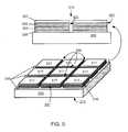
- FIG. 5shows a simplified diagram illustrating multiple unit cells formed from the layered structure by a laser separation process according to an embodiment of the present invention.
- This diagramis merely an example, which should not unduly limit the scope of the claims herein.
- the laser separation process mentioned in last paragraphhas removed a width of the layered structure within the portion 315 , which becomes one or more channels or trenches 515 cutting the layered structure down to the front surface region 220 .
- these one or more channels 515act as boundary regions of one or more unit cells 517 of the layered structure.
- a side viewalso shows in more detail of the unit cell structure after the laser separation process is performed on both edge region and inner grid-line region.
- each channelexposes a portion of the front surface region 220 and is sided with one or more cross-sectional region 501 .
- the cross-sectional region 501exposes every layers of the layered structure including the one or more films of the photovoltaic materials sandwiched by a metal layer beneath and another conductive layer on top.
- the cross-sectional region 501reveals the metal layer 305 , a P-type semiconductor layer 301 , an N-type semiconductor layer 303 , and a transparent conductive oxide layer 307 .
- the laser separation processis capable to provide the exposed portion of the front surface region 220 substantially free of residues of removed film materials during the laser separation process.
- the laser separation processis capable to provide the cross-sectional region 501 substantially free of residues of removed film materials which otherwise may cause conductive shorting between the layers resulting failure or damage to the solar device.
- the one or more unit cells 517possesses all device functionalities after laser separation from the continuous layered structure.
- the method 100includes providing one or more unit cells for manufacture of solar module. Essentially, the multiple unit cells 517 formed in a laser separation process to cut the layered structure 300 . Additionally, the laser separation process (processes 118 and 120 ), including any associated vacuum cleaning process, remove any residue of film materials from the cross-section region to prevent from any shorting between the layers.
- the layered structureincludes one or more P-N junctions among the one or more films of photovoltaic materials and includes at least one electrode layer made by a metal layer and another electrode layer made by a transparent conductive oxide layer. All the layers exposed at the cross-section region are substantially free of layer-shorting residue particles. Therefore, each unit cell 517 produced by the method 100 retains all the layered structures and by itself is capable of forming one unit photovoltaic cell of a solar module.
- Process 122 for providing one or more unit cells for manufacture of solar modulemay include transferring one or more unit cells out of the layered structure from the substrate.
- the transferred unit cellcan be packaged into or integrated with other devices or products to form a solar powered device or product.
- the thin film photovoltaic unit cellcan be implemented to a building material surface which can be used to build high energy efficient buildings from sky scraper to single family home.
- Process 122may also include coupling one unit cell with another electrically in series or in parallel to manufacture flexible solar module for different applications.
- FIG. 6shows an exemplary solar module including multiple unit cells cross linked with electric connectors according to an embodiment of the present invention.
- the solar module 600includes multiple unit cells ( 517 1 through 517 9 ) provided on a substrate 200 .
- each of the multiple unit cells 517 1 through 517 9are made from the unit 517 formed in Process 118 .
- the solar moduleincludes an electric connector 601 for coupling an electrode layer of one unit cell 517 1 on the upper right corner to either a neighboring unit cell within the solar module or another unit cell of a separate solar module.
- the whole right column of unit cells ( 517 1 through 517 3 ), as shown,is coupled electrically in parallel by one or more connectors 603 .
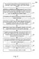
- FIG. 7is a simplified flowchart illustrating a method for manufacture of unit cells for thin film devices according to an alternative embodiment of the present invention.
- the method 700includes providing an optically transparent substrate having a thickness, a back surface region, and a front surface region ( 710 ).
- the optically transparent substratecan be the substrate 200 shown in FIG. 2 .
- the substrate usedmay be transparent to light with wavelength ranging from 400 nm to 1200 nm.
- the optical transparent substratecan be made of glass, or acrylic, or quartz, or fused silica or similar materials.
- a layered structure including one or more films of device materials sandwiched by a first conductive layer and a second conductive layeris formed spanning spatially overlying the front surface region ( 712 ) of the substrate.
- the first conductive layer directly overlying the front surface regioncan be a metal layer.
- the first conductive layercan also be transparent conductive oxide overlying the front surface region of an upstrate. This process can be substantially the same as the process 112 and the layered structure made by one or more films of photovoltaic materials can be substantially the same the layered structure 300 shown in FIG. 3 .
- the optically transparent substrate having the layered structure spatially overlying the front surface regionis then transferred ( 714 ) depending on the applications.
- the method 700further includes providing an optical opaque sheet material including one or more grid-line openings with a first width.
- the optical opaque sheet materialis disposed to immediate proximity of the back surface region.
- the optical opaque sheet materialis intended to block at least a light that is transparent to the substrate.
- the optical opaque sheet materialdoes not allow at least light with wavelength within 500 nm to 1200 nm to pass through.
- the process 716causes the one or more grid-line openings with a first width to be projected in a substantially vertical direction from the back surface region to the front surface region so that one or more cell-boundary regions can be defined with a width substantially the same as the first width.
- the defined cell boundary regionscan be the same as the grid-line regions 225 shown in FIG. 2 .
- the first widthis predetermined to be in a range from 1 mm to about 20 mm and more.
- the method 700includes a process 718 for illuminating a light beam substantially vertically onto a first region within the one or more grid-line openings.
- the light beamis a high powered laser beam generated from a mode-locked pulse laser source.
- the light beamis outputted from a laser source disposed near the back surface region and is aligned towards the first region within the one or more grid-line openings in a direction perpendicular to the back surface region.
- the laser sourcecan be a mode-locked Q-switched Nd:YAG laser source characterized by a wavelength ranging from 500 nm to 1200 nm, a pulse length ranging from nanoseconds to milliseconds, an energy density of about 50 W/cm 2 , and a homogeneous top-hat intensity profile.
- the laser beamcan have a beam spot size bigger than the first width of the grid-line openings within the optical opaque sheet material so that only partial beam may pass through the grid-line openings and further through the thickness of the transparent substrate.
- the beam spot sizecan be smaller than the designed width of the grid-line openings so that the beam needs to be scanned around to cover full width of the grid-line openings.
- the method 700includes a process 720 for subjecting at least partially the first conductive layer at a first portion within one or more cell boundary regions in the light beam to separate a column of the layered structure from the first portion.
- the laser powerafter passing through the transparent substrate and reaching the first region of the front surface region, can be absorbed by the first conductive layer immediately above the front surface region.
- At least a portion of the first conductive layerusually a metal layer with a strong absorbance band associated with the wavelength of the laser, can be heated in a very short time of a pulse length by absorbing energy from the high power density pulse laser.
- the heatat least partially is converted into latent heat of sublimation of the first conductive layer.
- the portion of the first conductive layeris sublimated or vaporized.
- the vaporized portionwould rapidly expand its volume and, assisted by the aligned laser beam, generate a strong mechanical force to break bonding of materials within the layered structure.
- a column of material of the layered structure within the first region directly above the sublimated portion of the first conductive layeris separated from the first region of the front surface region.
- the column of materialis broken apart into small pieces, particles, or dusts blown out of the continuous layered structure from the substrate, leaving behind a void column with a bottom and a surrounding side wall. The bottom is the exposed first region and the side wall is also an cross-sectional region of the remaining portion of the layered structure.
- the laser separation processis capable of freeing a portion of layered structure from the front surface region leaving behind an exposed area of front surface region and one or more cross-sectional regions substantially free of residues from the freed materials.
- a vacuum headcan be placed over the second conductive layer to suck out the blown out dusts or any residue particles. Because the high-power laser has a top-hat beam intensity profile over the whole beam size, the mechanical force generated in the laser separation process is highly-directional in parallel to the aligned laser beam so that the size of the resulted void column is substantially equal to the first region illuminated by the laser beam spot.
- the method 700includes a process ( 722 ) of scanning the light beam along the one or more grid-line openings to form one or more channels along the one or more cell-boundary regions.
- Scanningessentially performs repeating laser separation processes step by step.
- the scanning speedneeds to be adjusted based on the characteristics of the selected laser beam as well as the optical properties of film materials to be removed.
- the laser beam intensity profileis a critical factor to determine how much overlapping fraction for each illumination spot should be relative to an immediate last illumination spot before the laser beam scans or shifts.
- the beam spot sizealso affects the scanning routines for achieving a desired width of channel or trench by connecting a plurality of removed portions of layered structure, each being a void column formed by each beam illumination spot.
- the laser illumination and scanning routinescan cover a full first width of the grid-line openings so that a channel or trench with a second width can be formed along the projected cell-boundary regions.
- the second widthis substantially equal to the first width if the laser beam with top-hat beam profile is well aligned in the vertical direction to the back surface region.
- one or more channels with a widthranging from about 1 mm to about 20 mm and more can be formed by the laser separation process.
- the one or more channels or trenches formedare substantially similar to the trenches 515 shown in FIG. 5 .
- the laser illumination and scanningalso is performed along a full pattern of the grid-line openings to selectively remove a width of the layered structure to form all the channels along the whole cell-boundary regions.
- the scanning processis performed by controlling a mirror to guild the movement of the beam.
- the scanning processcan be performed by using a robot system to drive the stage that holds the substrate relative to a fixed laser beam.
- the stage movementallows the laser beam to irradiate at a first region within the grid-line openings and to move from the first region to a second region in a predetermined scanning procedure (with a planned pathway, spot coverage, and scanning speed).
- the scanning processis operated to allow the beam to irradiate within grid-line openings from a first region to a second region.
- the specific film material property, provided grid pattern, and selection of the pulsed laser sourceone can precisely control the dimension of ablated portion within the layered structure.
- the method 700further includes a Process 724 for forming one or more unit cells of the layered structure.
- the one or more channels formed within the continuous layered structureexpose a portion of front surface region and also create one or more cross-sectional regions of the remaining portion of the layered structure as their side walls.
- the exposed portion of the front surface regionsmaps with the cell-boundary regions defined in Process 716 .
- the cross-sectional regionsretain all the films and layers of the layered structure formed in Process 712 .
- the cross-sectional region formed using the method 700has a straight-edge shape substantially vertical to the substrate. The laser separation process can be tuned to form the one more channels with substantially free of residue particles therein.
- a vacuum headcan be applied and disposed above the layered structure subjecting to the laser separation process.
- nearly all the residues from the blown out materials or dusts during the laser separation processcan be immediately sucked away to leave a cleaned local region within each laser illumination spot.
- each channel along the one or more cell-boundary regionshave an exposed portion of the front surface region substantially free of residue particles and side walls also substantially free of residue particles. This is important because any residue particles falling on the cross-sectional region may cause electrical shorting or other damage to device.
- each unit structureincludes essentially the same one or more films of device materials sandwiched by the first conductive layer and the second conductive layer, and a peripheral side region free of layer-shorting particles from any residue of blown-out film materials. Therefore, each unit by itself is fully capable of performing all device functions as a single device.
- each unit cellacts as a thin film photovoltaic cell when the layered structure is one or more P-N junctions made of photovoltaic materials sandwiched by a bottom electrode layer and a top electrode layer.
- the method 700includes a process 726 for proving one or more unit cells for manufacture of a module device.
- one or more unit structuremay be transferred out of the continuous layered structure from the substrate.
- one or more unit structurecan be coupled to each other.
- each cross-sectional regionis clean and free of layer-shorting particles.
- One or more electric connectorsmay be inserted into the channels or trenches at the cell boundary regions to couple either the top electrode layer (e.g., the second conductive layer) or a bottom electrode layer (e.g., the first conductive layer).
- the coupling type of available plurality of unit cellscan be electrically in series or electrically in parallel so that the solar module formed by the process can have different operation current/voltage characteristics.
- one unit cell in one module devicemay be further coupled to another unit cell in a neighboring module device to make a module system.
- the layered structureincludes photovoltaic materials so that each unit cell can serve as a photovoltaic cell.
- FIG. 8is an exemplary optical microscope image of a channel formed in the thin film device by laser separation according to an embodiment of the present invention.
- This diagramis merely an example, which should not unduly limit the scope of the claims herein.
- a channel 810(bright color region) is formed by the laser separation process as a laser beam scans in one direction step by step across the thin film device 820 (dark color region) from the back surface region of the transparent substrate.
- the thin film materialhas been substantially removed from the transparent substrate, making it fully bright as illuminated by the microscope light.
- the thin film materials 820remain intact (and opaque to the microscope illumination light) without any sign of crack and residual particle decoration, as evidenced by the sharp contrast of the edges.
- the two dashed circles 831 and 832is schematically indicate the two subsequent beam spots during the scanning.
- the beam scanning speedis about 4 meters per second.
- the power up to 20 W laser irradiationis on with a pulse frequency of about 125 kHz.
- an overlapping region 83has an estimate 20% population of each beam size (the beam diameter is about 3 mm).
- such scanning laser beam spotscan be placed within the grid pattern pre-selected for manufacturing the multiple unit cells.
- a sequential two dimensional laser scanningcan create desired patterns with desired widths as the boundary regions of the unit cells out of the continuous thin film on the substrate.
Landscapes
- Engineering & Computer Science (AREA)
- Physics & Mathematics (AREA)
- Optics & Photonics (AREA)
- Plasma & Fusion (AREA)
- Mechanical Engineering (AREA)
- Laser Beam Processing (AREA)
Abstract
Description
Claims (13)
Priority Applications (1)
| Application Number | Priority Date | Filing Date | Title |
|---|---|---|---|
| US12/389,201US8075723B1 (en) | 2008-03-03 | 2009-02-19 | Laser separation method for manufacture of unit cells for thin film photovoltaic materials |
Applications Claiming Priority (2)
| Application Number | Priority Date | Filing Date | Title |
|---|---|---|---|
| US3340608P | 2008-03-03 | 2008-03-03 | |
| US12/389,201US8075723B1 (en) | 2008-03-03 | 2009-02-19 | Laser separation method for manufacture of unit cells for thin film photovoltaic materials |
Publications (1)
| Publication Number | Publication Date |
|---|---|
| US8075723B1true US8075723B1 (en) | 2011-12-13 |
Family
ID=45092634
Family Applications (1)
| Application Number | Title | Priority Date | Filing Date |
|---|---|---|---|
| US12/389,201Expired - Fee RelatedUS8075723B1 (en) | 2008-03-03 | 2009-02-19 | Laser separation method for manufacture of unit cells for thin film photovoltaic materials |
Country Status (1)
| Country | Link |
|---|---|
| US (1) | US8075723B1 (en) |
Cited By (5)
| Publication number | Priority date | Publication date | Assignee | Title |
|---|---|---|---|---|
| US20090231631A1 (en)* | 2008-03-13 | 2009-09-17 | Walter Psyk | Method for forming the separating lines of a photovoltaic module with series-connected cells |
| US20150194547A1 (en)* | 2012-11-05 | 2015-07-09 | Solexel, Inc. | Systems and methods for monolithically isled solar photovoltaic cells |
| US20160343704A1 (en)* | 2015-05-18 | 2016-11-24 | Azur Space Solar Power Gmbh | Scalable voltage source |
| US9515217B2 (en) | 2012-11-05 | 2016-12-06 | Solexel, Inc. | Monolithically isled back contact back junction solar cells |
| CN120152433A (en)* | 2025-05-12 | 2025-06-13 | 浙江晶科能源有限公司 | Method for manufacturing solar cell, solar cell and photovoltaic module |
Citations (94)
| Publication number | Priority date | Publication date | Assignee | Title |
|---|---|---|---|---|
| US4335266A (en) | 1980-12-31 | 1982-06-15 | The Boeing Company | Methods for forming thin-film heterojunction solar cells from I-III-VI.sub.2 |
| DE3314197A1 (en) | 1982-04-28 | 1983-11-03 | Energy Conversion Devices, Inc., 48084 Troy, Mich. | P-CONDUCTING AMORPHOUS SILICON ALLOY WITH A LARGE BAND GAP AND MANUFACTURING PROCESS THEREFOR |
| US4441113A (en) | 1981-02-13 | 1984-04-03 | Energy Conversion Devices, Inc. | P-Type semiconductor material having a wide band gap |
| US4461922A (en) | 1983-02-14 | 1984-07-24 | Atlantic Richfield Company | Solar cell module |
| US4465575A (en) | 1981-09-21 | 1984-08-14 | Atlantic Richfield Company | Method for forming photovoltaic cells employing multinary semiconductor films |
| US4471155A (en) | 1983-04-15 | 1984-09-11 | Energy Conversion Devices, Inc. | Narrow band gap photovoltaic devices with enhanced open circuit voltage |
| US4499658A (en) | 1983-09-06 | 1985-02-19 | Atlantic Richfield Company | Solar cell laminates |
| US4507181A (en) | 1984-02-17 | 1985-03-26 | Energy Conversion Devices, Inc. | Method of electro-coating a semiconductor device |
| US4517403A (en) | 1983-05-16 | 1985-05-14 | Atlantic Richfield Company | Series connected solar cells and method of formation |
| US4532372A (en) | 1983-12-23 | 1985-07-30 | Energy Conversion Devices, Inc. | Barrier layer for photovoltaic devices |
| US4542255A (en) | 1984-01-03 | 1985-09-17 | Atlantic Richfield Company | Gridded thin film solar cell |
| US4581108A (en) | 1984-01-06 | 1986-04-08 | Atlantic Richfield Company | Process of forming a compound semiconductive material |
| US4589194A (en) | 1983-12-29 | 1986-05-20 | Atlantic Richfield Company | Ultrasonic scribing of thin film solar cells |
| US4589918A (en) | 1984-03-28 | 1986-05-20 | National Research Institute For Metals | Thermal shock resistant thermoelectric material |
| US4598306A (en) | 1983-07-28 | 1986-07-01 | Energy Conversion Devices, Inc. | Barrier layer for photovoltaic devices |
| US4599154A (en) | 1985-03-15 | 1986-07-08 | Atlantic Richfield Company | Electrically enhanced liquid jet processing |
| US4611091A (en) | 1984-12-06 | 1986-09-09 | Atlantic Richfield Company | CuInSe2 thin film solar cell with thin CdS and transparent window layer |
| US4612411A (en) | 1985-06-04 | 1986-09-16 | Atlantic Richfield Company | Thin film solar cell with ZnO window layer |
| US4623601A (en) | 1985-06-04 | 1986-11-18 | Atlantic Richfield Company | Photoconductive device containing zinc oxide transparent conductive layer |
| US4625070A (en) | 1985-08-30 | 1986-11-25 | Atlantic Richfield Company | Laminated thin film solar module |
| US4638111A (en) | 1985-06-04 | 1987-01-20 | Atlantic Richfield Company | Thin film solar cell module |
| US4661370A (en) | 1984-02-08 | 1987-04-28 | Atlantic Richfield Company | Electric discharge processing of thin films |
| US4663495A (en) | 1985-06-04 | 1987-05-05 | Atlantic Richfield Company | Transparent photovoltaic module |
| US4724011A (en) | 1983-05-16 | 1988-02-09 | Atlantic Richfield Company | Solar cell interconnection by discrete conductive regions |
| US4751149A (en) | 1985-06-04 | 1988-06-14 | Atlantic Richfield Company | Chemical vapor deposition of zinc oxide films and products |
| US4775425A (en) | 1987-07-27 | 1988-10-04 | Energy Conversion Devices, Inc. | P and n-type microcrystalline semiconductor alloy material including band gap widening elements, devices utilizing same |
| US4798660A (en) | 1985-07-16 | 1989-01-17 | Atlantic Richfield Company | Method for forming Cu In Se2 films |
| US4816082A (en) | 1987-08-19 | 1989-03-28 | Energy Conversion Devices, Inc. | Thin film solar cell including a spatially modulated intrinsic layer |
| US4914042A (en) | 1986-09-30 | 1990-04-03 | Colorado State University Research Foundation | Forming a transition metal silicide radiation detector and source |
| US4915745A (en) | 1988-09-22 | 1990-04-10 | Atlantic Richfield Company | Thin film solar cell and method of making |
| US4950615A (en) | 1989-02-06 | 1990-08-21 | International Solar Electric Technology, Inc. | Method and making group IIB metal - telluride films and solar cells |
| FR2646560A1 (en) | 1989-04-27 | 1990-11-02 | Solems Sa | METHOD FOR IMPROVING THE SPECTRAL RESPONSE OF AN IMPROVED PHOTOCONDUCTOR STRUCTURE, SOLAR CELL AND PHOTORECEPTIVE STRUCTURE |
| US4996108A (en) | 1989-01-17 | 1991-02-26 | Simon Fraser University | Sheets of transition metal dichalcogenides |
| US5008062A (en) | 1988-01-20 | 1991-04-16 | Siemens Solar Industries, L.P. | Method of fabricating photovoltaic module |
| US5028274A (en) | 1989-06-07 | 1991-07-02 | International Solar Electric Technology, Inc. | Group I-III-VI2 semiconductor films for solar cell application |
| US5029760A (en) | 1989-10-26 | 1991-07-09 | Gamblin Rodger L | Centrifugal grinding and mixing apparatus |
| US5045409A (en) | 1987-11-27 | 1991-09-03 | Atlantic Richfield Company | Process for making thin film solar cell |
| US5069868A (en) | 1988-03-30 | 1991-12-03 | Idemitsu Petrolchemical Co., Ltd. | Method for producing thermoelectric elements |
| US5078803A (en) | 1989-09-22 | 1992-01-07 | Siemens Solar Industries L.P. | Solar cells incorporating transparent electrodes comprising hazy zinc oxide |
| US5125984A (en) | 1990-05-31 | 1992-06-30 | Siemens Aktiengesellschaft | Induced junction chalcopyrite solar cell |
| US5133809A (en) | 1989-10-07 | 1992-07-28 | Showa Shell Sekiyu K.K. | Photovoltaic device and process for manufacturing the same |
| US5137835A (en) | 1990-07-24 | 1992-08-11 | Siemens Aktiengesellschaft | Method for manufacturing a chalcopyrite solar cell |
| US5180686A (en) | 1988-10-31 | 1993-01-19 | Energy Conversion Devices, Inc. | Method for continuously deposting a transparent oxide material by chemical pyrolysis |
| US5211824A (en) | 1991-10-31 | 1993-05-18 | Siemens Solar Industries L.P. | Method and apparatus for sputtering of a liquid |
| US5231047A (en) | 1991-12-19 | 1993-07-27 | Energy Conversion Devices, Inc. | High quality photovoltaic semiconductor material and laser ablation method of fabrication same |
| US5248345A (en) | 1990-10-17 | 1993-09-28 | Showa Shell Sekiyu K.K. | Integrated photovoltaic device |
| US5261968A (en) | 1992-01-13 | 1993-11-16 | Photon Energy, Inc. | Photovoltaic cell and method |
| US5298086A (en) | 1992-05-15 | 1994-03-29 | United Solar Systems Corporation | Method for the manufacture of improved efficiency tandem photovoltaic device and device manufactured thereby |
| US5336623A (en) | 1992-03-02 | 1994-08-09 | Showa Shell Sekiyu K.K. | Process for producing integrated solar cell |
| US5346853A (en) | 1992-06-29 | 1994-09-13 | United Solar Systems Corporation | Microwave energized deposition process with substrate temperature control for the fabrication of P-I-N photovoltaic devices |
| US5474939A (en) | 1992-12-30 | 1995-12-12 | Siemens Solar Industries International | Method of making thin film heterojunction solar cell |
| US5501744A (en) | 1992-01-13 | 1996-03-26 | Photon Energy, Inc. | Photovoltaic cell having a p-type polycrystalline layer with large crystals |
| US5512107A (en) | 1992-03-19 | 1996-04-30 | Siemens Solar Gmbh | Environmentally stable thin-film solar module |
| US5536333A (en) | 1992-05-12 | 1996-07-16 | Solar Cells, Inc. | Process for making photovoltaic devices and resultant product |
| US5665175A (en) | 1990-05-30 | 1997-09-09 | Safir; Yakov | Bifacial solar cell |
| US5977476A (en) | 1996-10-16 | 1999-11-02 | United Solar Systems Corporation | High efficiency photovoltaic device |
| JP2000173969A (en) | 1998-12-03 | 2000-06-23 | Canon Inc | Rinse method and photovoltaic device |
| JP2000219512A (en) | 1998-11-24 | 2000-08-08 | Canon Inc | Method for manufacturing zinc oxide thin film, method for manufacturing photovoltaic device using the same, and photovoltaic device |
| US6166319A (en) | 1997-08-01 | 2000-12-26 | Canon Kabushiki Kaisha | Multi-junction photovoltaic device with microcrystalline I-layer |
| US6288415B1 (en) | 1996-10-24 | 2001-09-11 | University Of Surrey | Optoelectronic semiconductor devices |
| US6294274B1 (en) | 1998-11-16 | 2001-09-25 | Tdk Corporation | Oxide thin film |
| US6328871B1 (en) | 1999-08-16 | 2001-12-11 | Applied Materials, Inc. | Barrier layer for electroplating processes |
| US20020063065A1 (en) | 2000-09-19 | 2002-05-30 | Yuichi Sonoda | Method of forming zinc oxide film and process for producing photovoltaic device using it |
| JP2002167695A (en) | 2000-09-19 | 2002-06-11 | Canon Inc | Method for forming zinc oxide film and method for manufacturing photovoltaic element using the same |
| DE10104726A1 (en) | 2001-02-02 | 2002-08-08 | Siemens Solar Gmbh | Process for structuring an oxide layer applied to a carrier material |
| JP2002270871A (en) | 2001-03-12 | 2002-09-20 | Canon Inc | Semiconductor element and method of forming silicon-based thin film |
| US20030075717A1 (en) | 2001-03-12 | 2003-04-24 | Takaharu Kondo | Semiconductor element, and method of forming silicon-based film |
| US20040063320A1 (en) | 2002-09-30 | 2004-04-01 | Hollars Dennis R. | Manufacturing apparatus and method for large-scale production of thin-film solar cells |
| US20040095658A1 (en) | 2002-09-05 | 2004-05-20 | Nanosys, Inc. | Nanocomposites |
| US6784492B1 (en) | 1991-03-18 | 2004-08-31 | Canon Kabushiki Kaisha | Semiconductor device including a gate-insulated transistor |
| US20040203220A1 (en) | 2003-01-16 | 2004-10-14 | Tdk Corporation | Method of making iron silicide and method of making photoelectric transducer |
| JP2004332043A (en) | 2003-05-07 | 2004-11-25 | Canon Inc | Method and apparatus for forming zinc oxide thin film, and method for forming photovoltaic element |
| US20040244826A1 (en) | 2002-06-19 | 2004-12-09 | Jfe Steel Corporation | Beta-iron disilicate thermoelectric transducing material and thermoelectric transducer |
| US20040245912A1 (en) | 2003-04-01 | 2004-12-09 | Innovalight | Phosphor materials and illumination devices made therefrom |
| US20040252488A1 (en) | 2003-04-01 | 2004-12-16 | Innovalight | Light-emitting ceiling tile |
| US6852920B2 (en) | 2002-06-22 | 2005-02-08 | Nanosolar, Inc. | Nano-architected/assembled solar electricity cell |
| US6878871B2 (en) | 2002-09-05 | 2005-04-12 | Nanosys, Inc. | Nanostructure and nanocomposite based compositions and photovoltaic devices |
| US20050164432A1 (en) | 2000-08-22 | 2005-07-28 | President And Fellows Of Harvard College | Doped elongated semiconductors, growing such semiconductors, devices including such semiconductors and fabricating such devices |
| US20050287717A1 (en) | 2004-06-08 | 2005-12-29 | Nanosys, Inc. | Methods and devices for forming nanostructure monolayers and devices including such monolayers |
| US20060002838A1 (en) | 2002-09-11 | 2006-01-05 | Nikko Materials Co., Ltd. | Iron silicide powder and method for production thereof |
| US20060034065A1 (en) | 2004-08-10 | 2006-02-16 | Innovalight, Inc. | Light strips for lighting and backlighting applications |
| US20060040103A1 (en) | 2004-06-08 | 2006-02-23 | Nanosys, Inc. | Post-deposition encapsulation of nanostructures: compositions, devices and systems incorporating same |
| US20060051505A1 (en) | 2004-06-18 | 2006-03-09 | Uwe Kortshagen | Process and apparatus for forming nanoparticles using radiofrequency plasmas |
| US20060053969A1 (en) | 2002-11-28 | 2006-03-16 | Takashi Harada | Thermoelectric material and method for producing same |
| US20060220059A1 (en) | 2003-04-09 | 2006-10-05 | Matsushita Electric Industrial Co., Ltd | Solar cell |
| US20070006914A1 (en) | 2004-06-18 | 2007-01-11 | Lee Howard W | Nanostructured materials and photovoltaic devices including nanostructured materials |
| US7180101B2 (en) | 2002-04-25 | 2007-02-20 | Canon Kabushiki Kaisha | Semiconductor device, and method for manufacturing the same |
| US20070089782A1 (en) | 2003-10-02 | 2007-04-26 | Scheuten Glasgroep | Spherical or grain-shaped semiconductor element for use in solar cells and method for producing the same; method for producing a solar cell comprising said semiconductor element and solar cell |
| US20070151596A1 (en) | 2004-02-20 | 2007-07-05 | Sharp Kabushiki Kaisha | Substrate for photoelectric conversion device, photoelectric conversion device, and stacked photoelectric conversion device |
| US20070169810A1 (en) | 2004-02-19 | 2007-07-26 | Nanosolar, Inc. | High-throughput printing of semiconductor precursor layer by use of chalcogen-containing vapor |
| US7265037B2 (en) | 2003-06-20 | 2007-09-04 | The Regents Of The University Of California | Nanowire array and nanowire solar cells and methods for forming the same |
| US20080041446A1 (en) | 2006-08-09 | 2008-02-21 | Industrial Technology Research Institute | Dye-sensitized solar cells and method for fabricating same |
| US20080092953A1 (en) | 2006-05-15 | 2008-04-24 | Stion Corporation | Method and structure for thin film photovoltaic materials using bulk semiconductor materials |
| US20080092945A1 (en) | 2006-10-24 | 2008-04-24 | Applied Quantum Technology Llc | Semiconductor Grain and Oxide Layer for Photovoltaic Cells |
- 2009
- 2009-02-19USUS12/389,201patent/US8075723B1/ennot_activeExpired - Fee Related
Patent Citations (100)
| Publication number | Priority date | Publication date | Assignee | Title |
|---|---|---|---|---|
| US4335266A (en) | 1980-12-31 | 1982-06-15 | The Boeing Company | Methods for forming thin-film heterojunction solar cells from I-III-VI.sub.2 |
| US4441113A (en) | 1981-02-13 | 1984-04-03 | Energy Conversion Devices, Inc. | P-Type semiconductor material having a wide band gap |
| US4465575A (en) | 1981-09-21 | 1984-08-14 | Atlantic Richfield Company | Method for forming photovoltaic cells employing multinary semiconductor films |
| DE3314197A1 (en) | 1982-04-28 | 1983-11-03 | Energy Conversion Devices, Inc., 48084 Troy, Mich. | P-CONDUCTING AMORPHOUS SILICON ALLOY WITH A LARGE BAND GAP AND MANUFACTURING PROCESS THEREFOR |
| GB2124826A (en) | 1982-04-28 | 1984-02-22 | Energy Conversion Devices Inc | Amorphous semiconductor materials |
| US4461922A (en) | 1983-02-14 | 1984-07-24 | Atlantic Richfield Company | Solar cell module |
| US4471155A (en) | 1983-04-15 | 1984-09-11 | Energy Conversion Devices, Inc. | Narrow band gap photovoltaic devices with enhanced open circuit voltage |
| US4724011A (en) | 1983-05-16 | 1988-02-09 | Atlantic Richfield Company | Solar cell interconnection by discrete conductive regions |
| US4517403A (en) | 1983-05-16 | 1985-05-14 | Atlantic Richfield Company | Series connected solar cells and method of formation |
| US4598306A (en) | 1983-07-28 | 1986-07-01 | Energy Conversion Devices, Inc. | Barrier layer for photovoltaic devices |
| US4499658A (en) | 1983-09-06 | 1985-02-19 | Atlantic Richfield Company | Solar cell laminates |
| US4532372A (en) | 1983-12-23 | 1985-07-30 | Energy Conversion Devices, Inc. | Barrier layer for photovoltaic devices |
| US4589194A (en) | 1983-12-29 | 1986-05-20 | Atlantic Richfield Company | Ultrasonic scribing of thin film solar cells |
| US4542255A (en) | 1984-01-03 | 1985-09-17 | Atlantic Richfield Company | Gridded thin film solar cell |
| US4581108A (en) | 1984-01-06 | 1986-04-08 | Atlantic Richfield Company | Process of forming a compound semiconductive material |
| US4661370A (en) | 1984-02-08 | 1987-04-28 | Atlantic Richfield Company | Electric discharge processing of thin films |
| US4507181A (en) | 1984-02-17 | 1985-03-26 | Energy Conversion Devices, Inc. | Method of electro-coating a semiconductor device |
| US4589918A (en) | 1984-03-28 | 1986-05-20 | National Research Institute For Metals | Thermal shock resistant thermoelectric material |
| US4611091A (en) | 1984-12-06 | 1986-09-09 | Atlantic Richfield Company | CuInSe2 thin film solar cell with thin CdS and transparent window layer |
| US4599154A (en) | 1985-03-15 | 1986-07-08 | Atlantic Richfield Company | Electrically enhanced liquid jet processing |
| US4612411A (en) | 1985-06-04 | 1986-09-16 | Atlantic Richfield Company | Thin film solar cell with ZnO window layer |
| US4623601A (en) | 1985-06-04 | 1986-11-18 | Atlantic Richfield Company | Photoconductive device containing zinc oxide transparent conductive layer |
| US4751149A (en) | 1985-06-04 | 1988-06-14 | Atlantic Richfield Company | Chemical vapor deposition of zinc oxide films and products |
| US4638111A (en) | 1985-06-04 | 1987-01-20 | Atlantic Richfield Company | Thin film solar cell module |
| US4663495A (en) | 1985-06-04 | 1987-05-05 | Atlantic Richfield Company | Transparent photovoltaic module |
| US4798660A (en) | 1985-07-16 | 1989-01-17 | Atlantic Richfield Company | Method for forming Cu In Se2 films |
| US4625070A (en) | 1985-08-30 | 1986-11-25 | Atlantic Richfield Company | Laminated thin film solar module |
| US4914042A (en) | 1986-09-30 | 1990-04-03 | Colorado State University Research Foundation | Forming a transition metal silicide radiation detector and source |
| US4775425A (en) | 1987-07-27 | 1988-10-04 | Energy Conversion Devices, Inc. | P and n-type microcrystalline semiconductor alloy material including band gap widening elements, devices utilizing same |
| US4816082A (en) | 1987-08-19 | 1989-03-28 | Energy Conversion Devices, Inc. | Thin film solar cell including a spatially modulated intrinsic layer |
| US5045409A (en) | 1987-11-27 | 1991-09-03 | Atlantic Richfield Company | Process for making thin film solar cell |
| US5008062A (en) | 1988-01-20 | 1991-04-16 | Siemens Solar Industries, L.P. | Method of fabricating photovoltaic module |
| US5069868A (en) | 1988-03-30 | 1991-12-03 | Idemitsu Petrolchemical Co., Ltd. | Method for producing thermoelectric elements |
| US4915745A (en) | 1988-09-22 | 1990-04-10 | Atlantic Richfield Company | Thin film solar cell and method of making |
| US4915745B1 (en) | 1988-09-22 | 1992-04-07 | A Pollock Gary | |
| US5180686A (en) | 1988-10-31 | 1993-01-19 | Energy Conversion Devices, Inc. | Method for continuously deposting a transparent oxide material by chemical pyrolysis |
| US4996108A (en) | 1989-01-17 | 1991-02-26 | Simon Fraser University | Sheets of transition metal dichalcogenides |
| US4950615A (en) | 1989-02-06 | 1990-08-21 | International Solar Electric Technology, Inc. | Method and making group IIB metal - telluride films and solar cells |
| FR2646560A1 (en) | 1989-04-27 | 1990-11-02 | Solems Sa | METHOD FOR IMPROVING THE SPECTRAL RESPONSE OF AN IMPROVED PHOTOCONDUCTOR STRUCTURE, SOLAR CELL AND PHOTORECEPTIVE STRUCTURE |
| US5039353A (en) | 1989-04-27 | 1991-08-13 | Societe Dite: Solems (Societe Anonyme) | Process for improving the spectral response of a photoconductive structure, and improved solar cell and photoreceptive structure |
| US5028274A (en) | 1989-06-07 | 1991-07-02 | International Solar Electric Technology, Inc. | Group I-III-VI2 semiconductor films for solar cell application |
| US5078803A (en) | 1989-09-22 | 1992-01-07 | Siemens Solar Industries L.P. | Solar cells incorporating transparent electrodes comprising hazy zinc oxide |
| US5133809A (en) | 1989-10-07 | 1992-07-28 | Showa Shell Sekiyu K.K. | Photovoltaic device and process for manufacturing the same |
| US5029760A (en) | 1989-10-26 | 1991-07-09 | Gamblin Rodger L | Centrifugal grinding and mixing apparatus |
| US5665175A (en) | 1990-05-30 | 1997-09-09 | Safir; Yakov | Bifacial solar cell |
| US5125984A (en) | 1990-05-31 | 1992-06-30 | Siemens Aktiengesellschaft | Induced junction chalcopyrite solar cell |
| US5137835A (en) | 1990-07-24 | 1992-08-11 | Siemens Aktiengesellschaft | Method for manufacturing a chalcopyrite solar cell |
| US5248345A (en) | 1990-10-17 | 1993-09-28 | Showa Shell Sekiyu K.K. | Integrated photovoltaic device |
| US6784492B1 (en) | 1991-03-18 | 2004-08-31 | Canon Kabushiki Kaisha | Semiconductor device including a gate-insulated transistor |
| US5211824A (en) | 1991-10-31 | 1993-05-18 | Siemens Solar Industries L.P. | Method and apparatus for sputtering of a liquid |
| US5231047A (en) | 1991-12-19 | 1993-07-27 | Energy Conversion Devices, Inc. | High quality photovoltaic semiconductor material and laser ablation method of fabrication same |
| US5261968A (en) | 1992-01-13 | 1993-11-16 | Photon Energy, Inc. | Photovoltaic cell and method |
| US5501744A (en) | 1992-01-13 | 1996-03-26 | Photon Energy, Inc. | Photovoltaic cell having a p-type polycrystalline layer with large crystals |
| US5336623A (en) | 1992-03-02 | 1994-08-09 | Showa Shell Sekiyu K.K. | Process for producing integrated solar cell |
| US5512107A (en) | 1992-03-19 | 1996-04-30 | Siemens Solar Gmbh | Environmentally stable thin-film solar module |
| US5536333A (en) | 1992-05-12 | 1996-07-16 | Solar Cells, Inc. | Process for making photovoltaic devices and resultant product |
| US5298086A (en) | 1992-05-15 | 1994-03-29 | United Solar Systems Corporation | Method for the manufacture of improved efficiency tandem photovoltaic device and device manufactured thereby |
| US5346853A (en) | 1992-06-29 | 1994-09-13 | United Solar Systems Corporation | Microwave energized deposition process with substrate temperature control for the fabrication of P-I-N photovoltaic devices |
| US5474939A (en) | 1992-12-30 | 1995-12-12 | Siemens Solar Industries International | Method of making thin film heterojunction solar cell |
| US5977476A (en) | 1996-10-16 | 1999-11-02 | United Solar Systems Corporation | High efficiency photovoltaic device |
| US6288415B1 (en) | 1996-10-24 | 2001-09-11 | University Of Surrey | Optoelectronic semiconductor devices |
| AU734676B2 (en) | 1997-08-01 | 2001-06-21 | Canon Kabushiki Kaisha | Photovoltaic element and method of producing same |
| US6166319A (en) | 1997-08-01 | 2000-12-26 | Canon Kabushiki Kaisha | Multi-junction photovoltaic device with microcrystalline I-layer |
| US6294274B1 (en) | 1998-11-16 | 2001-09-25 | Tdk Corporation | Oxide thin film |
| JP2000219512A (en) | 1998-11-24 | 2000-08-08 | Canon Inc | Method for manufacturing zinc oxide thin film, method for manufacturing photovoltaic device using the same, and photovoltaic device |
| JP2000173969A (en) | 1998-12-03 | 2000-06-23 | Canon Inc | Rinse method and photovoltaic device |
| US6328871B1 (en) | 1999-08-16 | 2001-12-11 | Applied Materials, Inc. | Barrier layer for electroplating processes |
| US20050164432A1 (en) | 2000-08-22 | 2005-07-28 | President And Fellows Of Harvard College | Doped elongated semiconductors, growing such semiconductors, devices including such semiconductors and fabricating such devices |
| US20020063065A1 (en) | 2000-09-19 | 2002-05-30 | Yuichi Sonoda | Method of forming zinc oxide film and process for producing photovoltaic device using it |
| JP2002167695A (en) | 2000-09-19 | 2002-06-11 | Canon Inc | Method for forming zinc oxide film and method for manufacturing photovoltaic element using the same |
| US20040110393A1 (en) | 2001-02-02 | 2004-06-10 | Adolf Munzer | Method for structuring an oxide layer applied to a substrate material |
| DE10104726A1 (en) | 2001-02-02 | 2002-08-08 | Siemens Solar Gmbh | Process for structuring an oxide layer applied to a carrier material |
| US20030075717A1 (en) | 2001-03-12 | 2003-04-24 | Takaharu Kondo | Semiconductor element, and method of forming silicon-based film |
| JP2002270871A (en) | 2001-03-12 | 2002-09-20 | Canon Inc | Semiconductor element and method of forming silicon-based thin film |
| US7180101B2 (en) | 2002-04-25 | 2007-02-20 | Canon Kabushiki Kaisha | Semiconductor device, and method for manufacturing the same |
| US20040244826A1 (en) | 2002-06-19 | 2004-12-09 | Jfe Steel Corporation | Beta-iron disilicate thermoelectric transducing material and thermoelectric transducer |
| US6852920B2 (en) | 2002-06-22 | 2005-02-08 | Nanosolar, Inc. | Nano-architected/assembled solar electricity cell |
| US6878871B2 (en) | 2002-09-05 | 2005-04-12 | Nanosys, Inc. | Nanostructure and nanocomposite based compositions and photovoltaic devices |
| US20040095658A1 (en) | 2002-09-05 | 2004-05-20 | Nanosys, Inc. | Nanocomposites |
| US20060002838A1 (en) | 2002-09-11 | 2006-01-05 | Nikko Materials Co., Ltd. | Iron silicide powder and method for production thereof |
| US20040063320A1 (en) | 2002-09-30 | 2004-04-01 | Hollars Dennis R. | Manufacturing apparatus and method for large-scale production of thin-film solar cells |
| US20060053969A1 (en) | 2002-11-28 | 2006-03-16 | Takashi Harada | Thermoelectric material and method for producing same |
| US20040203220A1 (en) | 2003-01-16 | 2004-10-14 | Tdk Corporation | Method of making iron silicide and method of making photoelectric transducer |
| US20060003585A1 (en) | 2003-01-16 | 2006-01-05 | Tdk Corporation | Method of making iron silicide and method of making photoelectric transducer |
| US20040252488A1 (en) | 2003-04-01 | 2004-12-16 | Innovalight | Light-emitting ceiling tile |
| US20040245912A1 (en) | 2003-04-01 | 2004-12-09 | Innovalight | Phosphor materials and illumination devices made therefrom |
| US20060220059A1 (en) | 2003-04-09 | 2006-10-05 | Matsushita Electric Industrial Co., Ltd | Solar cell |
| JP2004332043A (en) | 2003-05-07 | 2004-11-25 | Canon Inc | Method and apparatus for forming zinc oxide thin film, and method for forming photovoltaic element |
| US7265037B2 (en) | 2003-06-20 | 2007-09-04 | The Regents Of The University Of California | Nanowire array and nanowire solar cells and methods for forming the same |
| US20070089782A1 (en) | 2003-10-02 | 2007-04-26 | Scheuten Glasgroep | Spherical or grain-shaped semiconductor element for use in solar cells and method for producing the same; method for producing a solar cell comprising said semiconductor element and solar cell |
| US20070169810A1 (en) | 2004-02-19 | 2007-07-26 | Nanosolar, Inc. | High-throughput printing of semiconductor precursor layer by use of chalcogen-containing vapor |
| US20070151596A1 (en) | 2004-02-20 | 2007-07-05 | Sharp Kabushiki Kaisha | Substrate for photoelectric conversion device, photoelectric conversion device, and stacked photoelectric conversion device |
| US20060040103A1 (en) | 2004-06-08 | 2006-02-23 | Nanosys, Inc. | Post-deposition encapsulation of nanostructures: compositions, devices and systems incorporating same |
| US20050287717A1 (en) | 2004-06-08 | 2005-12-29 | Nanosys, Inc. | Methods and devices for forming nanostructure monolayers and devices including such monolayers |
| US20060051505A1 (en) | 2004-06-18 | 2006-03-09 | Uwe Kortshagen | Process and apparatus for forming nanoparticles using radiofrequency plasmas |
| US20070006914A1 (en) | 2004-06-18 | 2007-01-11 | Lee Howard W | Nanostructured materials and photovoltaic devices including nanostructured materials |
| US20060034065A1 (en) | 2004-08-10 | 2006-02-16 | Innovalight, Inc. | Light strips for lighting and backlighting applications |
| US20080092953A1 (en) | 2006-05-15 | 2008-04-24 | Stion Corporation | Method and structure for thin film photovoltaic materials using bulk semiconductor materials |
| US20080041446A1 (en) | 2006-08-09 | 2008-02-21 | Industrial Technology Research Institute | Dye-sensitized solar cells and method for fabricating same |
| US20080092945A1 (en) | 2006-10-24 | 2008-04-24 | Applied Quantum Technology Llc | Semiconductor Grain and Oxide Layer for Photovoltaic Cells |
Non-Patent Citations (15)
| Title |
|---|
| Chopra et al., Thin-Film Solar Cells: An Overview, 2004, Progress in Photovoltaics: Research and Applications, 2004, vol. 12, pp. 69-92. |
| Ellmer et al., Copper Indium Disulfide Solar Cell Absorbers Prepared in a One-Step Process by Reactive Magnetron Sputtering from Copper and Indium Targets; Elsevier Science B.V; Thin Solid Films 413 (2002) pp. 92-97. |
| Huang et al., Photoluminescence and Electroluminescence of ZnS:Cu Nanocrystals in Polymeric Networks, Applied Physics, Lett. 70 (18), May 5, 1997, pp. 2335-2337. |
| Huang et al., Preparation of ZnxCd1-xS Nanocomposites in Polymer Matrices and their Photophysical Properties, Langmuir 1998, 14, pp. 4342-4344. |
| Huang et al., Preparation of ZnxCd1—xS Nanocomposites in Polymer Matrices and their Photophysical Properties, Langmuir 1998, 14, pp. 4342-4344. |
| International Search Report & Written Opinion of PCT Application No. PCT/US 09/46161, date of mailing Jul. 27, 2009, 14 pages total. |
| International Search Report & Written Opinion of PCT Application No. PCT/US 09/46802, mailed on Jul. 31, 2009, 11 pages total. |
| International Search Report and Written Opinion of PCT Application No. PCT/US08/76908, date of mailing Dec. 1, 2008, 8 pages total. |
| International Search Report and Written Opinion of PCT Application No. PCT/US08/77965, date of mailing Dec. 9, 2008, 8 pages total. |
| International Search Report and Written Opinion of PCT Application No. PCT/US08/78019, date of mailing Dec. 8, 2008, 9 pages total. |
| International Search Report and Written Opinion of PCT Application No. PCT/US2008/078001, date of mailing Dec. 2, 2008, 7 pages total. |
| Onuma et al., Preparation and Characterization of CuInS Thin Films Solar Cells with Large Grain, Elsevier Science B.V; Solar Energy Materials & Solar Cells 69 (2001) pp. 261-269. |
| Yang et al., Electroluminescence from ZnS/CdS Nanocrystals/Polymer Composite, Synthetic Metals 91, (1997) 347-349. |
| Yang et al., Fabrication and Characteristics of ZnS Nanocrystals/Polymer Composite Doped with Tetraphenylbenzidine Single Layer Structure Light-emitting Diode, Applied Physics Lett. vol. 69 (3), Jul. 15, 1996, pp. 377-379. |
| Yang et al., Preparation, Characterization and Electroluminescence of ZnS Nanocrystals in a Polymer Matrix, J. Mater. Chem., 1997, 7(1), pp. 131-133. |
Cited By (8)
| Publication number | Priority date | Publication date | Assignee | Title |
|---|---|---|---|---|
| US20090231631A1 (en)* | 2008-03-13 | 2009-09-17 | Walter Psyk | Method for forming the separating lines of a photovoltaic module with series-connected cells |
| US8187911B2 (en)* | 2008-03-13 | 2012-05-29 | Schott Solar Ag | Method for forming the separating lines of a photovoltaic module with series-connected cells |
| US20150194547A1 (en)* | 2012-11-05 | 2015-07-09 | Solexel, Inc. | Systems and methods for monolithically isled solar photovoltaic cells |
| JP2016500931A (en)* | 2012-11-05 | 2016-01-14 | ソレクセル、インコーポレイテッド | System and method for integrated aisle photovoltaic cells and modules |
| US9515217B2 (en) | 2012-11-05 | 2016-12-06 | Solexel, Inc. | Monolithically isled back contact back junction solar cells |
| US20160343704A1 (en)* | 2015-05-18 | 2016-11-24 | Azur Space Solar Power Gmbh | Scalable voltage source |
| US10872887B2 (en)* | 2015-05-18 | 2020-12-22 | Azur Space Solar Power Gmbh | Scalable voltage source |
| CN120152433A (en)* | 2025-05-12 | 2025-06-13 | 浙江晶科能源有限公司 | Method for manufacturing solar cell, solar cell and photovoltaic module |
Similar Documents
| Publication | Publication Date | Title |
|---|---|---|
| US7855089B2 (en) | Application specific solar cell and method for manufacture using thin film photovoltaic materials | |
| US9379258B2 (en) | Fabrication methods for monolithically isled back contact back junction solar cells | |
| US9515217B2 (en) | Monolithically isled back contact back junction solar cells | |
| JP3414738B2 (en) | Integrated laser patterning method for thin film solar cells | |
| US9236510B2 (en) | Patterning of silicon oxide layers using pulsed laser ablation | |
| US20130130430A1 (en) | Spatially selective laser annealing applications in high-efficiency solar cells | |
| US9508886B2 (en) | Method for making a crystalline silicon solar cell substrate utilizing flat top laser beam | |
| US9455362B2 (en) | Laser irradiation aluminum doping for monocrystalline silicon substrates | |
| US20080029152A1 (en) | Laser scribing apparatus, systems, and methods | |
| US20120225515A1 (en) | Laser doping techniques for high-efficiency crystalline semiconductor solar cells | |
| KR101384853B1 (en) | Laser processing methods for photovoltaic solar cells | |
| TW201340177A (en) | Method for forming a localized melting zone in a crucible containing a plurality of types of impurities | |
| US8075723B1 (en) | Laser separation method for manufacture of unit cells for thin film photovoltaic materials | |
| US20130164883A1 (en) | Laser annealing applications in high-efficiency solar cells | |
| WO2014179368A1 (en) | Damage free laser patterning of transparent layers for forming doped regions on a solar cell substrate | |
| US20140273329A1 (en) | Solar cell laser scribing methods | |
| US9214585B2 (en) | Annealing for damage free laser processing for high efficiency solar cells | |
| KR20120003213A (en) | Solar cell module and manufacturing method thereof | |
| CN101689574A (en) | Method and apparatus for the laser scribing of ultra lightweight semiconductor devices | |
| US20170005206A1 (en) | Patterning of silicon oxide layers using pulsed laser ablation | |
| KR20110090933A (en) | Method for manufacturing photoelectric conversion device, device for manufacturing photoelectric conversion device and photoelectric conversion device | |
| KR20130027535A (en) | Laser processing for high-efficiency thin crystalline silicon solar cell fabrication | |
| KR101532721B1 (en) | Spatially selective laser annealing applications in high-efficiency solar cells | |
| EP2819181A1 (en) | Laser annealing applications in high-efficiency solar cells | |
| US8772078B1 (en) | Method and system for laser separation for exclusion region of multi-junction photovoltaic materials |
Legal Events
| Date | Code | Title | Description |
|---|---|---|---|
| AS | Assignment | Owner name:STION CORPORATION, CALIFORNIA Free format text:ASSIGNMENT OF ASSIGNORS INTEREST;ASSIGNOR:FARRIS, CHESTER A., III;REEL/FRAME:022395/0234 Effective date:20090313 | |
| AS | Assignment | Owner name:CM MANUFACTURING, INC., CALIFORNIA Free format text:CHANGE OF NAME;ASSIGNOR:STION CORPORATION;REEL/FRAME:032144/0774 Effective date:20131011 | |
| AS | Assignment | Owner name:HETF SOLAR INC., CALIFORNIA Free format text:SECURITY AGREEMENT;ASSIGNOR:DEVELOPMENT SPECIALIST, INC., SOLELY IN ITS CAPACITY AS THE ASSIGNEE FOR THE BENEFIT OF THE CREDITORS OF CM MANUFACTURING, INC. (F/K/A STION CORPORATION), AND CM MANUFACTURING (F/K/A STION CORPORATION);REEL/FRAME:032209/0879 Effective date:20131022 | |
| AS | Assignment | Owner name:STION CORPORATION, CALIFORNIA Free format text:CHANGE OF NAME;ASSIGNOR:HETF SOLAR INC.;REEL/FRAME:032324/0402 Effective date:20131025 | |
| REMI | Maintenance fee reminder mailed | ||
| LAPS | Lapse for failure to pay maintenance fees | ||
| STCH | Information on status: patent discontinuation | Free format text:PATENT EXPIRED DUE TO NONPAYMENT OF MAINTENANCE FEES UNDER 37 CFR 1.362 | |
| FP | Lapsed due to failure to pay maintenance fee | Effective date:20151213 |