US8072805B2 - Method and system of finding a read voltage for a flash memory - Google Patents
Method and system of finding a read voltage for a flash memoryDownload PDFInfo
- Publication number
- US8072805B2 US8072805B2US12/543,496US54349609AUS8072805B2US 8072805 B2US8072805 B2US 8072805B2US 54349609 AUS54349609 AUS 54349609AUS 8072805 B2US8072805 B2US 8072805B2
- Authority
- US
- United States
- Prior art keywords
- read voltage
- bit number
- state bit
- flash memory
- optimal
- Prior art date
- Legal status (The legal status is an assumption and is not a legal conclusion. Google has not performed a legal analysis and makes no representation as to the accuracy of the status listed.)
- Active, expires
Links
Images


Classifications
- G—PHYSICS
- G11—INFORMATION STORAGE
- G11C—STATIC STORES
- G11C16/00—Erasable programmable read-only memories
- G11C16/02—Erasable programmable read-only memories electrically programmable
- G11C16/06—Auxiliary circuits, e.g. for writing into memory
- G11C16/34—Determination of programming status, e.g. threshold voltage, overprogramming or underprogramming, retention
- G—PHYSICS
- G11—INFORMATION STORAGE
- G11C—STATIC STORES
- G11C11/00—Digital stores characterised by the use of particular electric or magnetic storage elements; Storage elements therefor
- G11C11/56—Digital stores characterised by the use of particular electric or magnetic storage elements; Storage elements therefor using storage elements with more than two stable states represented by steps, e.g. of voltage, current, phase, frequency
- G11C11/5621—Digital stores characterised by the use of particular electric or magnetic storage elements; Storage elements therefor using storage elements with more than two stable states represented by steps, e.g. of voltage, current, phase, frequency using charge storage in a floating gate
- G11C11/5642—Sensing or reading circuits; Data output circuits
- G—PHYSICS
- G11—INFORMATION STORAGE
- G11C—STATIC STORES
- G11C7/00—Arrangements for writing information into, or reading information out from, a digital store
- G11C7/10—Input/output [I/O] data interface arrangements, e.g. I/O data control circuits, I/O data buffers
- G11C7/1006—Data managing, e.g. manipulating data before writing or reading out, data bus switches or control circuits therefor
Definitions
- the present inventiongenerally relates to a flash memory, and more particularly to a method and system of finding an optimal read voltage for a flash memory.
- Flash memoryis a non-volatile solid state memory device that can be electrically erased and reprogrammed, and is a specific type of electrically erasable programmable read-only memory (EEPROM) device.
- EEPROMelectrically erasable programmable read-only memory
- Conventional flash memorystores a single bit of information in each memory cell such that each memory cell can be programmed to assume two possible states.
- the conventional flash memoryis thus commonly referred to as single-level cell (SLC) flash memory or single-bit cell (SBC) flash memory.
- SLCsingle-level cell
- SBCsingle-bit cell
- Modern flash memoryis capable of storing two or more bits of information in each memory cell such that each memory cell can be programmed to assume more than two possible states.
- the modern flash memoryis thus commonly referred to as multi-level cell (MLC) flash memory or multi-bit cell (MBC) flash memory.
- MLCmulti-level cell
- MLCmulti-bit cell
- the threshold voltage of each stateis not a constant value but a range.
- the threshold voltage of a cellis compared to read voltages to determine its state.
- the read voltages for reading data from the traditional MLC flash memoryare constant.
- the threshold voltage distributionmay probably change after the flash memory has been subjected to a predetermined number of program/erase cycles or/and a predetermined data retention time has elapsed.
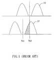
- the initial distribution 10 with read voltage Th 0may be suffered from retention issue after a long time not going through program/erase cycle, and therefore drifted downward to a shifted distribution 12 with a new read voltage Th 1 .
- a number of error bits(e.g., the shaded area) may incur if the initial read voltage Th 0 is still used to read data from the flash memory.
- dataare read from array cells of the flash memory with a default read voltage, and a recorded state bit number that is recorded during programming is also read. Determine whether the readout data passes error correction control (ECC), followed by determining an optimal read voltage if the readout data do not pass the ECC. Data are re-read from the array cells of the flash memory with the determined optimal read voltage.
- ECCerror correction control
- FIG. 1shows error bits accompanied with a shifted threshold voltage distribution
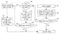
- FIG. 2Ais a flow diagram that illustrates a method of finding an optimal read voltage for a flash memory according to one embodiment of the present invention
- FIG. 2Bis a flow diagram that illustrates a method of finding an optimal read voltage for a flash memory according to an embodiment alternative to that in FIG. 2A ;
- FIG. 3Ashows a detailed flow diagram of the optimal read voltage determination step in FIG. 2A or FIG. 2B according to a first embodiment of the present invention
- FIG. 3Billustrates the concept of the failure bit number
- FIG. 3Cshows a further example that illustrates finding the failure ratio for a 3-bit MLC flash memory
- FIG. 4Ashows a detailed flow diagram of the optimal read voltage determination step in FIG. 2A or FIG. 2B according to a second embodiment of the present invention
- FIG. 4Bshows an example of finding the optimal read voltage by interpolation
- FIG. 4Cshows an example of finding the optimal read voltage by extrapolation
- FIG. 5Ashows a process of effectively reading a 3-bit MLC flash memory
- FIG. 5Bshows a sequence according to which the state bit numbers are programmed
- FIG. 6Ashows a block diagram that illustrates a system of finding an optimal read voltage for a flash memory according to the first embodiment with respect to FIG. 2 A/ 2 B and FIG. 3A ;
- FIG. 6Bshows a block diagram that illustrates a system of finding an optimal read voltage for a flash memory according to the second embodiment with respect to FIG. 2 A/ 2 B and FIG. 4A .
- FIG. 2Ais a flow diagram that illustrates a method of finding an optimal read voltage for a flash memory according to one embodiment of the present invention.
- the embodimentmay be adapted to a multi-level cell (MLC) flash memory as well as a single-level cell (SLC) flash memory.
- MLCmulti-level cell
- SLCsingle-level cell
- the step 21data are read from array cells of the flash memory with a default or original read voltage, and the bit number of each state that has been recorded beforehand in spare or redundant cells, during programming, is also read (the step 22 ). If the reading passes the error correction control (ECC), in the step 23 , that is applied to detect and correct error or errors, the reading finishes. Otherwise, an optimal read voltage is searched or determined in the step 24 . The determined optimal read voltage may be stored, for example, in a register before its use. Afterwards, the array cells of the flash memory are re-read, in the step 25 , using the determined read voltage.
- ECCerror correction control
- FIG. 2Bis a flow diagram that illustrates a method of finding an optimal read voltage for a flash memory according to an embodiment alternative to that in FIG. 2A .
- the step 26before the step 24 is performed, if any new read voltage exists (the step 26 ), then the existed read voltage may be used to re-read the flash memory (the step 27 ). For example, if an optimal read voltage has been determined for a neighboring page, that optimal read voltage may then be used for the present page to re-read the flash memory.
- the step 27determine whether the reading passes the error correction control (ECC) (the step 28 ). If the reading still does not pass the ECC, the read voltage searching step 24 is then performed.
- ECCerror correction control
- FIG. 3Ashows a detailed flow diagram of the step 24 (of FIG. 2A or FIG. 2B ) for determining the optimal read voltage according to a first embodiment of the present invention.
- a page(or any specific amount) is read from the flash memory many times using multiple read voltages respectively (the step 241 ).
- the (cumulative) bit numberse.g., N 1 , N 2 , etc.
- the read voltagese.g., V 1 , V 2 , etc.
- an optimal read voltage or offset voltageis determined according to a predetermined lookup table (LUT) that maps a failure ratio (or a failure bit number) to a read voltage (or offset voltage).
- LUTlookup table
- FIG. 3Billustrates the concept of the failure bit number. As shown in the figure, the recorded (cumulative) bit number of state “1” using a default read voltage V 0 is n, and the counted (cumulative) bit number of the state “1” using the read voltage V 1 is N 1 . Therefore, the failure ratio F 1 with respect to the read voltage V 1 is (N 1 ⁇ n)/n.
- the failure ratio F 2 with respect to a read voltage V 2is (N 2 ⁇ n)/n, where N 2 is the associated counted bit number of state “1.”
- a lookup tableis exemplified in the following Table 1. Specifically, the left column of Table 1 lists failure ratio with respect to each read voltage in the right column. Based on the lookup table, the optimal read voltage (or the offset voltage) may then be determined according to the failure ratio resulted from the reading in the step 241 .
- the failure ratio in the left column of Table 1may be replaced with the failure bit number if all the states are uniformly distributed such that all the state bit numbers n are substantially the same.
- the read voltage in the right columnmay be replaced with the offset voltage that is the difference between the read voltage and the default (or original) read voltage V 0 .
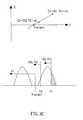
- FIG. 3Cshows a further example that illustrates finding the failure ratio for a 3-bit MLC flash memory that has 8 states.
- a 0is the recorded bit number for the state “1” that is recorded beforehand during the programming
- a 0 ′is the counted bit number for the state “1” during reading.
- the shaded area, or (A 0 ′ ⁇ a 0 )is the failure bit number of the state c 4 .
- the failure ratio of the state c 4is the ratio of the failure bit number to the bit number (c 4 ) of the state c 4 , or (A 0 ′ ⁇ a 0 )/c4.
- FIG. 4Ashows a detailed flow diagram of the step 24 (of FIG. 2 A or FIG. 2B ) for determining the optimal read voltage according to a second embodiment of the present invention.
- the flow diagram in FIG. 4Ais similar to that in FIG. 3A except that the step 243 is now replaced with the step 244 , in which the optimal read voltage is determined according to at least two sets of the recorded state bit number (during the programming) and the counted bit number (during the reading). For example, n 1 is the recorded bit number for the state “1,” N 1 is the first counted bit number for the state “1” using a first read voltage V 1 , and N 2 is the second counted bit number for the state “1” using a second read voltage V 2 .
- FIG. 4Ashows a detailed flow diagram of the step 24 (of FIG. 2 A or FIG. 2B ) for determining the optimal read voltage according to a second embodiment of the present invention.
- the flow diagram in FIG. 4Ais similar to that in FIG. 3
- FIG. 4Bshows an example in which the Y axis represents the counted state bit number minus the recorded state bit number, and the X axis represents the associated read voltage.
- the optimal interpolated read voltage V target between V 1 and V 2has a state bit number equal to the counted state bit number n 1 .
- FIG. 4Cshows a further example in which the optimal extrapolated read voltage V target of V 1 and V 2 has a state bit number equal to the recorded state bit number n 1 .
- interpolation/extrapolation optimization processis used in the embodiment, it is appreciated that other optimization process, such as linear regression analysis (LRA), maximum likelihood estimation (MLE), expectation maximization (EM) or binary search, may be used instead.
- LRAlinear regression analysis
- MLEmaximum likelihood estimation
- EMexpectation maximization
- an optimal read voltagemay be determined and then utilized to read the array cells of the flash memory with minimized failure (or error) bit number due to threshold voltage shift.
- FIG. 5Ashows a process of effectively reading a 3-bit MLC flash memory. Specifically, group A is read using read voltage V 3 ; followed by reading group B using read voltages V 1 and V 5 ; and finally group C is read using read voltages V 0 , V 2 , V 4 and V 6 .
- the state bit numbersare programmed in a sequence as illustrated in Table 2 and depicted in FIG. 5B . According to this program sequence, read margin and reliability for each state can be substantially maximized.
- the recorded space in the flash memorymay be minimized by reducing the recorded state bit number.
- Table 3shows an example in which only some portions of the state bit numbers are recorded, while other portions (that are in parenthesis) of the state bit numbers may be derived according to the recorded ones. Assume the page number is N, then the non-recorded state bit numbers may be derived as follows:
- FIG. 6Ashows a block diagram that illustrates a system 5 of finding an optimal read voltage for a flash memory according to the first embodiment with respect to FIG. 2 A/ 2 B and FIG. 3A .
- the system 5includes a flash memory 50 and a memory controller 52 .
- Datamay be programmed to or read from the flash memory 50 from/to a host (not shown) through the memory controller 52 .
- the flash memory 50the data being programmed to or read from the array cells (not shown) of the flash memory 50 may be temporarily stored in a page buffer 500 , and operation and timing of the flash memory 50 may be managed by control logic 502 .
- a data buffer 520is used for temporarily storing data and for interfacing with the flash memory 50
- control logic 522is used for managing the operation and timing of the memory controller 52 .
- the memory controller 52further includes a data pair ⁇ N,V> generator 524 that generates the (cumulative) bit numbers (e.g., N 1 , N 2 , etc.) respectively corresponding to the read voltages (e.g., V 1 , V 2 , etc.) in the step 242 ( FIG. 3A ).
- the memory controller 52also includes a read voltage decision device 528 that performs the step 243 ( FIG. 3A ) for determining the optimal read voltage or offset voltage according to a predetermined lookup table (LUT) 526 that maps a failure ratio (or a failure bit number) to a read voltage (or offset voltage).
- LUTlookup table
- FIG. 6Bshows a block diagram that illustrates a system 5 B of finding an optimal read voltage for a flash memory according to the second embodiment with respect to FIG. 2 A/ 2 B and FIG. 4A .
- the system 5 Bis similar to the system 5 except that the read voltage decision device 528 B performs the step 244 ( FIG. 4A ) for determining the optimal read voltage according to at least two sets of the recorded state bit number (during the programming) and the counted bit number (during the reading). In this second embodiment, no lookup table is need in the system 5 B.
Landscapes
- Engineering & Computer Science (AREA)
- Computer Hardware Design (AREA)
- Techniques For Improving Reliability Of Storages (AREA)
- Read Only Memory (AREA)
Abstract
Description
1. Field of the Invention
The present invention generally relates to a flash memory, and more particularly to a method and system of finding an optimal read voltage for a flash memory.
2. Description of the Prior Art
Flash memory is a non-volatile solid state memory device that can be electrically erased and reprogrammed, and is a specific type of electrically erasable programmable read-only memory (EEPROM) device. Conventional flash memory stores a single bit of information in each memory cell such that each memory cell can be programmed to assume two possible states. The conventional flash memory is thus commonly referred to as single-level cell (SLC) flash memory or single-bit cell (SBC) flash memory. Modern flash memory is capable of storing two or more bits of information in each memory cell such that each memory cell can be programmed to assume more than two possible states. The modern flash memory is thus commonly referred to as multi-level cell (MLC) flash memory or multi-bit cell (MBC) flash memory.
In the MLC flash memory, data of different state are programmed to the flash memory by storing different amount of charge in the floating gate of the flash memory. As the charge in the floating gate specifically determines the corresponding threshold voltage, the data can then be read from the MLC flash memory according to their different threshold voltage. Due to variations among the memory cells during the manufacture, operation or according to other factors, the threshold voltage of each state is not a constant value but a range. When the flash memory is being read, the threshold voltage of a cell is compared to read voltages to determine its state.
The read voltages for reading data from the traditional MLC flash memory are constant. In practice, however, the threshold voltage distribution may probably change after the flash memory has been subjected to a predetermined number of program/erase cycles or/and a predetermined data retention time has elapsed. For example, as shown inFIG. 1 (in which only two states are concerned and shown for illustrative purpose), theinitial distribution 10 with read voltage Th0 may be suffered from retention issue after a long time not going through program/erase cycle, and therefore drifted downward to a shifteddistribution 12 with a new read voltage Th1. A number of error bits (e.g., the shaded area) may incur if the initial read voltage Th0 is still used to read data from the flash memory.
For the reason that conventional MLC or SLC flash memory could probably result in read errors due to cycle/retention issue, a need has arisen to propose some novel schemes to obtain proper read voltages for reading data from the flash memory.
In view of the foregoing, it is an object of the present embodiment to provide a method and system of finding a proper or optimal read voltage for a flash memory in order to minimize the error bit number.
According to one embodiment, data are read from array cells of the flash memory with a default read voltage, and a recorded state bit number that is recorded during programming is also read. Determine whether the readout data passes error correction control (ECC), followed by determining an optimal read voltage if the readout data do not pass the ECC. Data are re-read from the array cells of the flash memory with the determined optimal read voltage.
Referring toFIG. 2A , after the flash memory is requested by a read command (the step21), data are read from array cells of the flash memory with a default or original read voltage, and the bit number of each state that has been recorded beforehand in spare or redundant cells, during programming, is also read (the step22). If the reading passes the error correction control (ECC), in thestep 23, that is applied to detect and correct error or errors, the reading finishes. Otherwise, an optimal read voltage is searched or determined in thestep 24. The determined optimal read voltage may be stored, for example, in a register before its use. Afterwards, the array cells of the flash memory are re-read, in thestep 25, using the determined read voltage.
| TABLE 1 | |||
| Failure ratio | Read voltage | ||
| F1 | V1 | ||
| F2 | V2 | ||
| F3 | V3 | ||
| . . . | . . . | ||
| Fn | Vn | ||
It is appreciated that the failure ratio in the left column of Table 1 may be replaced with the failure bit number if all the states are uniformly distributed such that all the state bit numbers n are substantially the same. Moreover, the read voltage in the right column may be replaced with the offset voltage that is the difference between the read voltage and the default (or original) read voltage V0.
According to the embodiments described above, an optimal read voltage may be determined and then utilized to read the array cells of the flash memory with minimized failure (or error) bit number due to threshold voltage shift.
In order to facilitate the effectiveness of programming/reading a MLC flash memory, an effective method of recording the state bit number is adopted in the embodiment.FIG. 5A shows a process of effectively reading a 3-bit MLC flash memory. Specifically, group A is read using read voltage V3; followed by reading group B using read voltages V1 and V5; and finally group C is read using read voltages V0, V2, V4 and V6. In order to make sure the correctness and the reliability, the state bit numbers are programmed in a sequence as illustrated in Table 2 and depicted inFIG. 5B . According to this program sequence, read margin and reliability for each state can be substantially maximized.
| TABLE 2 | ||
| bit number | ||
| to be | Program sequence | |
| recorded | state | A | C | |
| A | ||||
| 1 | 1 | 1 | 1 | |
| 0 | 0 | 1 | 1 | |
| 1 | 1 | 1 | 1 | |
| 0 | 1 | 0 | 1 | |
| 1 | 1 | 1 | 1 | |
| 0 | 1 | 1 | 0 | |
According to one aspect of the present embodiment, the recorded space in the flash memory may be minimized by reducing the recorded state bit number. Table 3 shows an example in which only some portions of the state bit numbers are recorded, while other portions (that are in parenthesis) of the state bit numbers may be derived according to the recorded ones. Assume the page number is N, then the non-recorded state bit numbers may be derived as follows:
- Group A; a1=N−a0;
- Group B: b1=a0−b0, b2=a1−b3=N−a0−b3;
- Group C: c1=b0−c0, c2=b1−c3=a0−b0−c3, c5=b2−c4=a1−b3−c4, c6=b3−c7.
| TABLE 3 | ||
| A | (a0) | a1 |
| B | (b0) | b1 | b2 | (b3) |
| C | (c0) | c1 | c2 | (c3) | (c4) | c5 | c6 | (c7) |
| A | 1 | 0 |
| 1 | 0 | 0 | 1 |
| 1 | 0 | 0 | 1 | 1 | 0 | 0 | 1 | |
Thememory controller 52 further includes a data pair <N,V>generator 524 that generates the (cumulative) bit numbers (e.g., N1, N2, etc.) respectively corresponding to the read voltages (e.g., V1, V2, etc.) in the step242 (FIG. 3A ). Thememory controller 52 also includes a readvoltage decision device 528 that performs the step243 (FIG. 3A ) for determining the optimal read voltage or offset voltage according to a predetermined lookup table (LUT)526 that maps a failure ratio (or a failure bit number) to a read voltage (or offset voltage).
Although specific embodiments have been illustrated and described, it will be appreciated by those skilled in the art that various modifications may be made without departing from the scope of the present invention, which is intended to be limited solely by the appended claims.
Claims (22)
1. A method of finding a read voltage for a flash memory, comprising:
reading data from array cells of the flash memory with a default read voltage;
reading a recorded state bit number of each state that is recorded during programming using the default read voltage;
determining whether the readout data passes error correction control (ECC); and
determining an optimal read voltage if the readout data do not pass the ECC, and re-reading data from the array cells of the flash memory with the determined optimal read voltage;
wherein the step of determining the optimal read voltage comprises:
reading a page at least one time using at least one associated read voltage for each time;
counting at least one state bit number respectively corresponding to the at least one read voltage; and
determining the optimal read voltage according to the recorded state bit number and the counted state bit number.
2. The method ofclaim 1 , wherein the flash memory is a multi-level cell (MLC) flash memory.
3. The method ofclaim 1 , further comprising a step of storing the determined optimal read voltage.
4. The method ofclaim 1 , before the step of determining the optimal read voltage, further comprising a step of re-reading data from the array cells of the flash memory with an existed read voltage.
5. The method ofclaim 1 , the step of determining the optimal read voltage further comprises:
determining the optimal read voltage according to a predetermined lookup table (LUT) that maps a failure ratio to one of the multiple read voltages.
6. The method ofclaim 5 , wherein the failure ratio is a ratio of failure bit number to the recorded state bit number.
7. The method ofclaim 5 , wherein the lookup table maps a failure bit number to one of the multiple read voltages.
8. The method ofclaim 1 , the step of determining the optimal read voltage further comprises:
determining the optimal read voltage according to at least two sets of the recorded state bit number and the counted state bit number.
9. The method ofclaim 8 , wherein interpolation or extrapolation is performed on the two sets of the recorded state bit number and the counted state bit number, resulting in an interpolated or extrapolated read voltage as the optimal read voltage corresponding to the recorded state bit number.
10. The method ofclaim 8 , wherein the optimal read voltage is determined according to a first difference of the recorded state bit number and a first counted state bit number, and a second difference of the recorded state bit number and a second counted state bit number.
11. The method ofclaim 1 , further comprising a step of deriving a state bit number according to the recorded state bit number and a page number.
12. A system of finding a read voltage for a flash memory, comprising:
a data buffer for storing data read from array cells of the flash memory with a default read voltage, and a recorded state bit number of each state that is recorded during programming using the default read voltage;
a read voltage decision device for:
determining whether the readout data passes error correction control (ECC); and
determining an optimal read voltage if the readout data do not pass the ECC, and re-reading data from the array cells of the flash memory with the determined optimal read voltage;
a data pair generator for reading a page at least one time using at least one associated read voltage for each time, and counting at least one state bit numbers respectively corresponding to the at least one read voltage, wherein the optimal read voltage is determined according to the recorded state bit number and the counted state bit number.
13. The system ofclaim 12 , wherein the flash memory is a multi-level cell (MLC) flash memory.
14. The system ofclaim 12 , further comprising a register for storing the determined optimal read voltage.
15. The system ofclaim 12 , before the optimal read voltage is determined, the read voltage decision device further re-reads data from the array cells of the flash memory with an existed read voltage.
16. The system ofclaim 12 , further comprising:
a lookup table that maps a failure ratio to one of the multiple read voltages, wherein the lookup table is used for determining the optimal read voltage.
17. The system ofclaim 16 , wherein the failure ratio is a ratio of failure bit number to the recorded state bit number.
18. The system ofclaim 16 , wherein a lookup table maps a failure bit number to one of the multiple read voltages.
19. The system ofclaim 12 ,
wherein the optimal read voltage is determined according to at least two sets of the recorded state bit number and the counted state bit number.
20. The system ofclaim 19 , wherein the read voltage decision device performs interpolation or extrapolation on the two sets of the recorded state bit number and the counted state bit number, resulting in an interpolated or extrapolated read voltage as the optimal read voltage corresponding to the recorded state bit number.
21. The system ofclaim 19 , wherein the optimal read voltage is determined according to a first difference of the recorded state bit number and a first counted state bit number, and a second difference of the recorded state bit number and a second counted state bit number.
22. The system ofclaim 12 , wherein the read voltage decision device further derives a state bit number according to the recorded state bit number and a page number.
Priority Applications (2)
| Application Number | Priority Date | Filing Date | Title |
|---|---|---|---|
| US12/543,496US8072805B2 (en) | 2009-08-18 | 2009-08-18 | Method and system of finding a read voltage for a flash memory |
| TW098131456ATWI370453B (en) | 2009-08-18 | 2009-09-18 | Method and system of finding a read voltage for a flash memory |
Applications Claiming Priority (1)
| Application Number | Priority Date | Filing Date | Title |
|---|---|---|---|
| US12/543,496US8072805B2 (en) | 2009-08-18 | 2009-08-18 | Method and system of finding a read voltage for a flash memory |
Publications (2)
| Publication Number | Publication Date |
|---|---|
| US20110044101A1 US20110044101A1 (en) | 2011-02-24 |
| US8072805B2true US8072805B2 (en) | 2011-12-06 |
Family
ID=43605279
Family Applications (1)
| Application Number | Title | Priority Date | Filing Date |
|---|---|---|---|
| US12/543,496Active2030-04-03US8072805B2 (en) | 2009-08-18 | 2009-08-18 | Method and system of finding a read voltage for a flash memory |
Country Status (2)
| Country | Link |
|---|---|
| US (1) | US8072805B2 (en) |
| TW (1) | TWI370453B (en) |
Cited By (72)
| Publication number | Priority date | Publication date | Assignee | Title |
|---|---|---|---|---|
| US20110066899A1 (en)* | 2009-09-17 | 2011-03-17 | Samsung Electronics Co., Ltd. | Nonvolatile memory system and related method of performing erase refresh operation |
| US20120236656A1 (en)* | 2010-07-09 | 2012-09-20 | Stec, Inc. | Apparatus and method for determining a read level of a memory cell based on cycle information |
| US8576625B1 (en)* | 2010-04-20 | 2013-11-05 | Marvell International Ltd. | Decoder parameter estimation using multiple memory reads |
| US20140043903A1 (en)* | 2012-08-07 | 2014-02-13 | Samsung Electronics Co., Ltd. | Memory device having variable read voltage and related methods of operation |
| US8665650B2 (en) | 2011-02-18 | 2014-03-04 | Marvell World Trade Ltd. | Reliability metrics management for soft decoding |
| US8737141B2 (en) | 2010-07-07 | 2014-05-27 | Stec, Inc. | Apparatus and method for determining an operating condition of a memory cell based on cycle information |
| US8819503B2 (en) | 2010-07-02 | 2014-08-26 | Stec, Inc. | Apparatus and method for determining an operating condition of a memory cell based on cycle information |
| US8909851B2 (en) | 2011-02-08 | 2014-12-09 | SMART Storage Systems, Inc. | Storage control system with change logging mechanism and method of operation thereof |
| US8935466B2 (en) | 2011-03-28 | 2015-01-13 | SMART Storage Systems, Inc. | Data storage system with non-volatile memory and method of operation thereof |
| US8949689B2 (en) | 2012-06-11 | 2015-02-03 | SMART Storage Systems, Inc. | Storage control system with data management mechanism and method of operation thereof |
| US20150049548A1 (en)* | 2013-08-16 | 2015-02-19 | Sang-Won Park | Read Methods for Non-Volatile Memory Devices and Related Non-Volatile Memory Devices |
| US20150052387A1 (en)* | 2013-08-14 | 2015-02-19 | Infineon Technologies Ag | Systems and methods utilizing a flexible read reference for a dynamic read window |
| US9021319B2 (en) | 2011-09-02 | 2015-04-28 | SMART Storage Systems, Inc. | Non-volatile memory management system with load leveling and method of operation thereof |
| US9021231B2 (en) | 2011-09-02 | 2015-04-28 | SMART Storage Systems, Inc. | Storage control system with write amplification control mechanism and method of operation thereof |
| US9043780B2 (en) | 2013-03-27 | 2015-05-26 | SMART Storage Systems, Inc. | Electronic system with system modification control mechanism and method of operation thereof |
| US9047955B2 (en) | 2011-03-30 | 2015-06-02 | Stec, Inc. | Adjusting operating parameters for memory cells based on wordline address and cycle information |
| US9063844B2 (en) | 2011-09-02 | 2015-06-23 | SMART Storage Systems, Inc. | Non-volatile memory management system with time measure mechanism and method of operation thereof |
| US9070479B2 (en) | 2013-01-21 | 2015-06-30 | Sandisk Technologies Inc. | Systems and methods of updating read voltages |
| US9098399B2 (en) | 2011-08-31 | 2015-08-04 | SMART Storage Systems, Inc. | Electronic system with storage management mechanism and method of operation thereof |
| US9123445B2 (en) | 2013-01-22 | 2015-09-01 | SMART Storage Systems, Inc. | Storage control system with data management mechanism and method of operation thereof |
| US9147490B2 (en)* | 2013-03-15 | 2015-09-29 | Sandisk Technologies Inc. | System and method of determining reading voltages of a data storage device |
| US9146850B2 (en) | 2013-08-01 | 2015-09-29 | SMART Storage Systems, Inc. | Data storage system with dynamic read threshold mechanism and method of operation thereof |
| US9152555B2 (en) | 2013-11-15 | 2015-10-06 | Sandisk Enterprise IP LLC. | Data management with modular erase in a data storage system |
| US9170941B2 (en) | 2013-04-05 | 2015-10-27 | Sandisk Enterprises IP LLC | Data hardening in a storage system |
| US9183137B2 (en) | 2013-02-27 | 2015-11-10 | SMART Storage Systems, Inc. | Storage control system with data management mechanism and method of operation thereof |
| US9195586B2 (en) | 2012-02-23 | 2015-11-24 | Hgst Technologies Santa Ana, Inc. | Determining bias information for offsetting operating variations in memory cells based on wordline address |
| US9214965B2 (en) | 2013-02-20 | 2015-12-15 | Sandisk Enterprise Ip Llc | Method and system for improving data integrity in non-volatile storage |
| US9239781B2 (en) | 2012-02-07 | 2016-01-19 | SMART Storage Systems, Inc. | Storage control system with erase block mechanism and method of operation thereof |
| US9244519B1 (en) | 2013-06-25 | 2016-01-26 | Smart Storage Systems. Inc. | Storage system with data transfer rate adjustment for power throttling |
| US9298252B2 (en) | 2012-04-17 | 2016-03-29 | SMART Storage Systems, Inc. | Storage control system with power down mechanism and method of operation thereof |
| US9313874B2 (en) | 2013-06-19 | 2016-04-12 | SMART Storage Systems, Inc. | Electronic system with heat extraction and method of manufacture thereof |
| US9330775B2 (en) | 2013-01-14 | 2016-05-03 | Samsung Electronics Co., Ltd. | Flash memory, flash memory system and operating method of the same |
| US9329928B2 (en) | 2013-02-20 | 2016-05-03 | Sandisk Enterprise IP LLC. | Bandwidth optimization in a non-volatile memory system |
| US9361222B2 (en) | 2013-08-07 | 2016-06-07 | SMART Storage Systems, Inc. | Electronic system with storage drive life estimation mechanism and method of operation thereof |
| US9367353B1 (en) | 2013-06-25 | 2016-06-14 | Sandisk Technologies Inc. | Storage control system with power throttling mechanism and method of operation thereof |
| US9412471B2 (en) | 2013-03-15 | 2016-08-09 | Samsung Electronics Co., Ltd. | Method of reading data from a nonvolatile memory device, nonvolatile memory device, and method of operating a memory system |
| US9431113B2 (en) | 2013-08-07 | 2016-08-30 | Sandisk Technologies Llc | Data storage system with dynamic erase block grouping mechanism and method of operation thereof |
| US9448946B2 (en) | 2013-08-07 | 2016-09-20 | Sandisk Technologies Llc | Data storage system with stale data mechanism and method of operation thereof |
| US9470720B2 (en) | 2013-03-08 | 2016-10-18 | Sandisk Technologies Llc | Test system with localized heating and method of manufacture thereof |
| US9519576B2 (en) | 2013-02-19 | 2016-12-13 | Samsung Electronics Co., Ltd. | Memory controller, method of operating the same and memory system including the same |
| US9543025B2 (en) | 2013-04-11 | 2017-01-10 | Sandisk Technologies Llc | Storage control system with power-off time estimation mechanism and method of operation thereof |
| US9576671B2 (en) | 2014-11-20 | 2017-02-21 | Western Digital Technologies, Inc. | Calibrating optimal read levels |
| US9606864B2 (en) | 2012-10-08 | 2017-03-28 | Samsung Electronics Co., Ltd. | Non-volatile memory device having adjustable read voltage, memory system comprising same, and method of operating same |
| US9671962B2 (en) | 2012-11-30 | 2017-06-06 | Sandisk Technologies Llc | Storage control system with data management mechanism of parity and method of operation thereof |
| US9715341B2 (en) | 2014-10-29 | 2017-07-25 | Samsung Electronics Co., Ltd. | Operating a memory device using a program order stamp to control a read voltage |
| US9720754B2 (en) | 2014-11-20 | 2017-08-01 | Western Digital Technologies, Inc. | Read level grouping for increased flash performance |
| US9792995B1 (en) | 2016-04-26 | 2017-10-17 | Sandisk Technologies Llc | Independent multi-plane read and low latency hybrid read |
| US9852804B2 (en) | 2015-12-04 | 2017-12-26 | Samsung Electronics Co., Ltd. | Nonvolatile memory device, memory system, method of operating nonvolatile memory device, and method of operating memory system |
| US9858014B2 (en) | 2014-10-29 | 2018-01-02 | Samsung Electronics Co., Ltd. | Memory system and method of operating same using program order information |
| US9898056B2 (en) | 2013-06-19 | 2018-02-20 | Sandisk Technologies Llc | Electronic assembly with thermal channel and method of manufacture thereof |
| US9905302B2 (en) | 2014-11-20 | 2018-02-27 | Western Digital Technologies, Inc. | Read level grouping algorithms for increased flash performance |
| US9921749B2 (en) | 2014-10-29 | 2018-03-20 | Samsung Electronics Co., Ltd. | Memory system and method including determining a read voltage based on program order information and a plurality of mapping tables |
| US10049037B2 (en) | 2013-04-05 | 2018-08-14 | Sandisk Enterprise Ip Llc | Data management in a storage system |
| US10424388B2 (en) | 2016-10-18 | 2019-09-24 | Samsung Electronics Co., Ltd. | Storage device, memory system, and read voltage decision method thereof |
| US10529432B2 (en) | 2016-02-17 | 2020-01-07 | Samsung Electronics Co., Ltd. | Data storage device including read voltage search unit |
| US10546648B2 (en) | 2013-04-12 | 2020-01-28 | Sandisk Technologies Llc | Storage control system with data management mechanism and method of operation thereof |
| DE102016003366B4 (en)* | 2015-03-20 | 2020-10-29 | Western Digital Technologies, Inc. (n.d.Ges.d.Staates Delaware) | READING LEVEL GROUPING FOR INCREASED FLASH PERFORMANCE |
| CN112447239A (en)* | 2019-09-03 | 2021-03-05 | 爱思开海力士有限公司 | Storage device and operation method thereof |
| US20210134377A1 (en)* | 2019-10-30 | 2021-05-06 | International Business Machines Corporation | Updating corrective read voltage offsets in non-volatile random access memory |
| US11017865B2 (en)* | 2019-09-03 | 2021-05-25 | SK Hynix Inc. | Memory controller determining optimal read voltage and operating method thereof |
| US11127476B2 (en)* | 2019-09-13 | 2021-09-21 | Kioxia Corporation | Memory system controlling a threshold voltage in a read operation and method |
| US11170857B2 (en)* | 2016-08-29 | 2021-11-09 | Kioxia Corporation | Semiconductor memory device that performs successive tracking reads during an operation to read one page |
| US11210210B2 (en) | 2017-11-27 | 2021-12-28 | Huawei Technologies Co., Ltd. | Read latency reduction method and apparatus |
| US11217319B2 (en)* | 2020-02-28 | 2022-01-04 | SK Hynix Inc. | Read threshold optimization systems and methods by multi-dimensional search |
| US20220130482A1 (en)* | 2020-10-28 | 2022-04-28 | Micron Technology, Inc. | Global-local Read Calibration |
| US20220180953A1 (en)* | 2020-12-04 | 2022-06-09 | SK Hynix Inc. | Storage device and operating method thereof |
| US20220230695A1 (en)* | 2021-01-21 | 2022-07-21 | Samsung Electronics Co., Ltd. | Nonvolatile memory device, memory system including same, and operating method of nonvolatile memory device |
| US20220301650A1 (en)* | 2021-03-16 | 2022-09-22 | SK Hynix Inc. | Controller controlling semiconductor memory device and method of operating the controller |
| US20240029801A1 (en)* | 2022-07-20 | 2024-01-25 | Micron Technology, Inc. | Memory read calibration based on memory device-originated metrics characterizing voltage distributions |
| US11961553B2 (en) | 2021-10-15 | 2024-04-16 | Samsung Electronics Co., Ltd. | Method of searching read voltage of nonvolatile memory device using regression analysis and method of reading data from nonvolatile memory device using the same |
| US12067287B2 (en) | 2021-08-17 | 2024-08-20 | Samsung Electronics Co., Ltd. | Memory controller calculating optimal read level, memory system including the same, and operating method of memory controller |
| US12424287B2 (en) | 2022-11-15 | 2025-09-23 | Micron Technology, Inc. | Memory read voltage threshold tracking based on memory device-originated metrics characterizing voltage distributions |
Families Citing this family (23)
| Publication number | Priority date | Publication date | Assignee | Title |
|---|---|---|---|---|
| US9245653B2 (en) | 2010-03-15 | 2016-01-26 | Intelligent Intellectual Property Holdings 2 Llc | Reduced level cell mode for non-volatile memory |
| KR20120046868A (en)* | 2010-10-29 | 2012-05-11 | 에스케이하이닉스 주식회사 | Semiconductor memory apparatus, semiconductor system and method of sensing data |
| US9135998B2 (en) | 2010-11-09 | 2015-09-15 | Micron Technology, Inc. | Sense operation flags in a memory device |
| US8358542B2 (en) | 2011-01-14 | 2013-01-22 | Micron Technology, Inc. | Methods, devices, and systems for adjusting sensing voltages in devices |
| US8631288B2 (en) | 2011-03-14 | 2014-01-14 | Micron Technology, Inc. | Methods, devices, and systems for data sensing in a memory system |
| EP2549482B1 (en) | 2011-07-22 | 2018-05-23 | SanDisk Technologies LLC | Apparatus, system and method for determining a configuration parameter for solid-state storage media |
| KR101892038B1 (en) | 2012-01-30 | 2018-08-27 | 삼성전자주식회사 | Method of reading data in a nonvolatile memory device |
| US8681569B2 (en)* | 2012-02-22 | 2014-03-25 | Silicon Motion, Inc. | Method for reading data stored in a flash memory according to a threshold voltage distribution and memory controller and system thereof |
| KR102038408B1 (en)* | 2012-10-25 | 2019-10-30 | 삼성전자주식회사 | Semiconductor memory system using regression alalysis and read method thereof |
| US9263136B1 (en) | 2013-09-04 | 2016-02-16 | Western Digital Technologies, Inc. | Data retention flags in solid-state drives |
| TWI492234B (en) | 2014-04-21 | 2015-07-11 | Silicon Motion Inc | Method, memory controller and memory system for reading data stored in flash memory |
| KR102293082B1 (en)* | 2014-07-29 | 2021-08-26 | 삼성전자주식회사 | Storage device, operation method of storage device and accessing method for accessing storage device |
| US9632867B2 (en)* | 2014-12-08 | 2017-04-25 | Cypress Semiconductor Corporation | Methods, circuits, devices, systems and machine executable code for reading from a non-volatile memory array |
| JP6378102B2 (en)* | 2015-01-28 | 2018-08-22 | 東芝メモリ株式会社 | Semiconductor device and reading method |
| CN106653087A (en)* | 2015-10-28 | 2017-05-10 | 光宝电子(广州)有限公司 | A solid state memory device and a related reading and controlling method thereof |
| KR102695928B1 (en)* | 2016-12-19 | 2024-08-16 | 삼성전자주식회사 | Read operation method of nonvoltile memory, memory system including the same and operation method thereof |
| KR102663813B1 (en)* | 2017-01-13 | 2024-05-07 | 삼성전자주식회사 | Non-volatile memory device for reading operation with optimized read voltage |
| KR102070307B1 (en)* | 2018-05-28 | 2020-01-23 | 에센코어 리미티드 | Method of operating storage unit |
| CN113010101B (en)* | 2019-12-20 | 2025-01-28 | 美光科技公司 | Managing read voltage levels of data cells in memory devices using programming time proximity |
| US11521700B2 (en)* | 2021-01-04 | 2022-12-06 | Innogrit Technologies Co., Ltd. | Reference voltage adjustment based on post-decoding and pre-decoding state information |
| US11355216B1 (en)* | 2021-04-06 | 2022-06-07 | Beijing Tenafe Electronic Technology Co., Ltd. | Adaptive DSP generation of read thresholds for gaussian and non-gaussian distributions in solid state storage using cumulative observed counts |
| CN113223583B (en)* | 2021-05-14 | 2024-05-17 | 深圳市硅格半导体有限公司 | Method for re-reading data in NAND FLASH bad blocks, electronic equipment and storage medium |
| CN113342569B (en)* | 2021-06-17 | 2022-02-11 | 哈尔滨工业大学 | Equal-length coding and decoding method for eliminating unreliable state of flash memory cell |
Citations (3)
| Publication number | Priority date | Publication date | Assignee | Title |
|---|---|---|---|---|
| WO2008111058A2 (en) | 2007-03-12 | 2008-09-18 | Anobit Technologies Ltd. | Adaptive estimation of memory cell read thresholds |
| US20080263266A1 (en) | 2007-04-23 | 2008-10-23 | Sandisk Il Ltd. | Adaptive dynamic reading of flash memories |
| US20090003058A1 (en)* | 2007-06-28 | 2009-01-01 | Samsung Electronics Co., Ltd. | Flash memory device and method for adjusting read voltage of flash memory device |
- 2009
- 2009-08-18USUS12/543,496patent/US8072805B2/enactiveActive
- 2009-09-18TWTW098131456Apatent/TWI370453B/enactive
Patent Citations (3)
| Publication number | Priority date | Publication date | Assignee | Title |
|---|---|---|---|---|
| WO2008111058A2 (en) | 2007-03-12 | 2008-09-18 | Anobit Technologies Ltd. | Adaptive estimation of memory cell read thresholds |
| US20080263266A1 (en) | 2007-04-23 | 2008-10-23 | Sandisk Il Ltd. | Adaptive dynamic reading of flash memories |
| US20090003058A1 (en)* | 2007-06-28 | 2009-01-01 | Samsung Electronics Co., Ltd. | Flash memory device and method for adjusting read voltage of flash memory device |
Cited By (93)
| Publication number | Priority date | Publication date | Assignee | Title |
|---|---|---|---|---|
| US20110066899A1 (en)* | 2009-09-17 | 2011-03-17 | Samsung Electronics Co., Ltd. | Nonvolatile memory system and related method of performing erase refresh operation |
| US8621266B2 (en)* | 2009-09-17 | 2013-12-31 | Samsung Electronics Co., Ltd. | Nonvolatile memory system and related method of performing erase refresh operation |
| US9153336B1 (en) | 2010-04-20 | 2015-10-06 | Marvell International Ltd. | Decoder parameter estimation using multiple memory reads |
| US8576625B1 (en)* | 2010-04-20 | 2013-11-05 | Marvell International Ltd. | Decoder parameter estimation using multiple memory reads |
| US8819503B2 (en) | 2010-07-02 | 2014-08-26 | Stec, Inc. | Apparatus and method for determining an operating condition of a memory cell based on cycle information |
| US9389938B2 (en) | 2010-07-07 | 2016-07-12 | Hgst Technologies Santa Ana, Inc. | Apparatus and method for determining an operating condition of a memory cell based on cycle information |
| US8737141B2 (en) | 2010-07-07 | 2014-05-27 | Stec, Inc. | Apparatus and method for determining an operating condition of a memory cell based on cycle information |
| US8737136B2 (en)* | 2010-07-09 | 2014-05-27 | Stec, Inc. | Apparatus and method for determining a read level of a memory cell based on cycle information |
| US20120236656A1 (en)* | 2010-07-09 | 2012-09-20 | Stec, Inc. | Apparatus and method for determining a read level of a memory cell based on cycle information |
| US8644099B2 (en) | 2010-07-09 | 2014-02-04 | Stec, Inc. | Apparatus and method for determining a read level of a flash memory after an inactive period of time |
| US8909851B2 (en) | 2011-02-08 | 2014-12-09 | SMART Storage Systems, Inc. | Storage control system with change logging mechanism and method of operation thereof |
| US8665650B2 (en) | 2011-02-18 | 2014-03-04 | Marvell World Trade Ltd. | Reliability metrics management for soft decoding |
| US9087598B2 (en) | 2011-02-18 | 2015-07-21 | Marvell World Trade Ltd. | Reliability metrics management for soft decoding |
| US8935466B2 (en) | 2011-03-28 | 2015-01-13 | SMART Storage Systems, Inc. | Data storage system with non-volatile memory and method of operation thereof |
| US9224456B2 (en) | 2011-03-30 | 2015-12-29 | Hgst Technologies Santa Ana, Inc. | Setting operating parameters for memory cells based on wordline address and cycle information |
| US9047955B2 (en) | 2011-03-30 | 2015-06-02 | Stec, Inc. | Adjusting operating parameters for memory cells based on wordline address and cycle information |
| US9098399B2 (en) | 2011-08-31 | 2015-08-04 | SMART Storage Systems, Inc. | Electronic system with storage management mechanism and method of operation thereof |
| US9021231B2 (en) | 2011-09-02 | 2015-04-28 | SMART Storage Systems, Inc. | Storage control system with write amplification control mechanism and method of operation thereof |
| US9063844B2 (en) | 2011-09-02 | 2015-06-23 | SMART Storage Systems, Inc. | Non-volatile memory management system with time measure mechanism and method of operation thereof |
| US9021319B2 (en) | 2011-09-02 | 2015-04-28 | SMART Storage Systems, Inc. | Non-volatile memory management system with load leveling and method of operation thereof |
| US9239781B2 (en) | 2012-02-07 | 2016-01-19 | SMART Storage Systems, Inc. | Storage control system with erase block mechanism and method of operation thereof |
| US9377962B2 (en) | 2012-02-23 | 2016-06-28 | Hgst Technologies Santa Ana, Inc. | Determining bias information for offsetting operating variations in memory cells |
| US9195586B2 (en) | 2012-02-23 | 2015-11-24 | Hgst Technologies Santa Ana, Inc. | Determining bias information for offsetting operating variations in memory cells based on wordline address |
| US9298252B2 (en) | 2012-04-17 | 2016-03-29 | SMART Storage Systems, Inc. | Storage control system with power down mechanism and method of operation thereof |
| US8949689B2 (en) | 2012-06-11 | 2015-02-03 | SMART Storage Systems, Inc. | Storage control system with data management mechanism and method of operation thereof |
| US20140043903A1 (en)* | 2012-08-07 | 2014-02-13 | Samsung Electronics Co., Ltd. | Memory device having variable read voltage and related methods of operation |
| US9190160B2 (en)* | 2012-08-07 | 2015-11-17 | Samsung Electronics Co., Ltd. | Memory device having variable read voltage and related methods of operation |
| US9606864B2 (en) | 2012-10-08 | 2017-03-28 | Samsung Electronics Co., Ltd. | Non-volatile memory device having adjustable read voltage, memory system comprising same, and method of operating same |
| US9671962B2 (en) | 2012-11-30 | 2017-06-06 | Sandisk Technologies Llc | Storage control system with data management mechanism of parity and method of operation thereof |
| US9812213B2 (en) | 2013-01-14 | 2017-11-07 | Samsung Electronics Co., Ltd. | Flash memory, flash memory system and operating method of the same |
| US9330775B2 (en) | 2013-01-14 | 2016-05-03 | Samsung Electronics Co., Ltd. | Flash memory, flash memory system and operating method of the same |
| US9070479B2 (en) | 2013-01-21 | 2015-06-30 | Sandisk Technologies Inc. | Systems and methods of updating read voltages |
| US9123445B2 (en) | 2013-01-22 | 2015-09-01 | SMART Storage Systems, Inc. | Storage control system with data management mechanism and method of operation thereof |
| US9519576B2 (en) | 2013-02-19 | 2016-12-13 | Samsung Electronics Co., Ltd. | Memory controller, method of operating the same and memory system including the same |
| US9214965B2 (en) | 2013-02-20 | 2015-12-15 | Sandisk Enterprise Ip Llc | Method and system for improving data integrity in non-volatile storage |
| US9329928B2 (en) | 2013-02-20 | 2016-05-03 | Sandisk Enterprise IP LLC. | Bandwidth optimization in a non-volatile memory system |
| US9183137B2 (en) | 2013-02-27 | 2015-11-10 | SMART Storage Systems, Inc. | Storage control system with data management mechanism and method of operation thereof |
| US9470720B2 (en) | 2013-03-08 | 2016-10-18 | Sandisk Technologies Llc | Test system with localized heating and method of manufacture thereof |
| US9147490B2 (en)* | 2013-03-15 | 2015-09-29 | Sandisk Technologies Inc. | System and method of determining reading voltages of a data storage device |
| US9412471B2 (en) | 2013-03-15 | 2016-08-09 | Samsung Electronics Co., Ltd. | Method of reading data from a nonvolatile memory device, nonvolatile memory device, and method of operating a memory system |
| TWI631564B (en)* | 2013-03-15 | 2018-08-01 | 南韓商三星電子股份有限公司 | Method of reading data from a nonvolatile memory device, nonvolatile memory device, and method of operating a memory system |
| US9043780B2 (en) | 2013-03-27 | 2015-05-26 | SMART Storage Systems, Inc. | Electronic system with system modification control mechanism and method of operation thereof |
| US9170941B2 (en) | 2013-04-05 | 2015-10-27 | Sandisk Enterprises IP LLC | Data hardening in a storage system |
| US10049037B2 (en) | 2013-04-05 | 2018-08-14 | Sandisk Enterprise Ip Llc | Data management in a storage system |
| US9543025B2 (en) | 2013-04-11 | 2017-01-10 | Sandisk Technologies Llc | Storage control system with power-off time estimation mechanism and method of operation thereof |
| US10546648B2 (en) | 2013-04-12 | 2020-01-28 | Sandisk Technologies Llc | Storage control system with data management mechanism and method of operation thereof |
| US9313874B2 (en) | 2013-06-19 | 2016-04-12 | SMART Storage Systems, Inc. | Electronic system with heat extraction and method of manufacture thereof |
| US9898056B2 (en) | 2013-06-19 | 2018-02-20 | Sandisk Technologies Llc | Electronic assembly with thermal channel and method of manufacture thereof |
| US9367353B1 (en) | 2013-06-25 | 2016-06-14 | Sandisk Technologies Inc. | Storage control system with power throttling mechanism and method of operation thereof |
| US9244519B1 (en) | 2013-06-25 | 2016-01-26 | Smart Storage Systems. Inc. | Storage system with data transfer rate adjustment for power throttling |
| US9146850B2 (en) | 2013-08-01 | 2015-09-29 | SMART Storage Systems, Inc. | Data storage system with dynamic read threshold mechanism and method of operation thereof |
| US9431113B2 (en) | 2013-08-07 | 2016-08-30 | Sandisk Technologies Llc | Data storage system with dynamic erase block grouping mechanism and method of operation thereof |
| US9361222B2 (en) | 2013-08-07 | 2016-06-07 | SMART Storage Systems, Inc. | Electronic system with storage drive life estimation mechanism and method of operation thereof |
| US9665295B2 (en) | 2013-08-07 | 2017-05-30 | Sandisk Technologies Llc | Data storage system with dynamic erase block grouping mechanism and method of operation thereof |
| US9448946B2 (en) | 2013-08-07 | 2016-09-20 | Sandisk Technologies Llc | Data storage system with stale data mechanism and method of operation thereof |
| US10319460B2 (en)* | 2013-08-14 | 2019-06-11 | Infineon Technologies Ag | Systems and methods utilizing a flexible read reference for a dynamic read window |
| US20150052387A1 (en)* | 2013-08-14 | 2015-02-19 | Infineon Technologies Ag | Systems and methods utilizing a flexible read reference for a dynamic read window |
| US20150049548A1 (en)* | 2013-08-16 | 2015-02-19 | Sang-Won Park | Read Methods for Non-Volatile Memory Devices and Related Non-Volatile Memory Devices |
| US9152555B2 (en) | 2013-11-15 | 2015-10-06 | Sandisk Enterprise IP LLC. | Data management with modular erase in a data storage system |
| US9921749B2 (en) | 2014-10-29 | 2018-03-20 | Samsung Electronics Co., Ltd. | Memory system and method including determining a read voltage based on program order information and a plurality of mapping tables |
| US9858014B2 (en) | 2014-10-29 | 2018-01-02 | Samsung Electronics Co., Ltd. | Memory system and method of operating same using program order information |
| US9715341B2 (en) | 2014-10-29 | 2017-07-25 | Samsung Electronics Co., Ltd. | Operating a memory device using a program order stamp to control a read voltage |
| US9720754B2 (en) | 2014-11-20 | 2017-08-01 | Western Digital Technologies, Inc. | Read level grouping for increased flash performance |
| US9905302B2 (en) | 2014-11-20 | 2018-02-27 | Western Digital Technologies, Inc. | Read level grouping algorithms for increased flash performance |
| US10566061B2 (en) | 2014-11-20 | 2020-02-18 | Western Digital Technologies, Inc. | Calibrating optimal read levels |
| US9576671B2 (en) | 2014-11-20 | 2017-02-21 | Western Digital Technologies, Inc. | Calibrating optimal read levels |
| US11488673B2 (en) | 2014-11-20 | 2022-11-01 | Western Digital Technologies, Inc. | Calibrating optimal read levels |
| DE102016003366B4 (en)* | 2015-03-20 | 2020-10-29 | Western Digital Technologies, Inc. (n.d.Ges.d.Staates Delaware) | READING LEVEL GROUPING FOR INCREASED FLASH PERFORMANCE |
| US9852804B2 (en) | 2015-12-04 | 2017-12-26 | Samsung Electronics Co., Ltd. | Nonvolatile memory device, memory system, method of operating nonvolatile memory device, and method of operating memory system |
| US10529432B2 (en) | 2016-02-17 | 2020-01-07 | Samsung Electronics Co., Ltd. | Data storage device including read voltage search unit |
| US10043558B2 (en) | 2016-04-26 | 2018-08-07 | Sandisk Technologies Llc | Independent multi-plane read and low latency hybrid read |
| US9792995B1 (en) | 2016-04-26 | 2017-10-17 | Sandisk Technologies Llc | Independent multi-plane read and low latency hybrid read |
| US11170857B2 (en)* | 2016-08-29 | 2021-11-09 | Kioxia Corporation | Semiconductor memory device that performs successive tracking reads during an operation to read one page |
| US10424388B2 (en) | 2016-10-18 | 2019-09-24 | Samsung Electronics Co., Ltd. | Storage device, memory system, and read voltage decision method thereof |
| US11210210B2 (en) | 2017-11-27 | 2021-12-28 | Huawei Technologies Co., Ltd. | Read latency reduction method and apparatus |
| CN112447239A (en)* | 2019-09-03 | 2021-03-05 | 爱思开海力士有限公司 | Storage device and operation method thereof |
| US11017865B2 (en)* | 2019-09-03 | 2021-05-25 | SK Hynix Inc. | Memory controller determining optimal read voltage and operating method thereof |
| US10998057B2 (en)* | 2019-09-03 | 2021-05-04 | SK Hynix Inc. | Storage device and method of operating the same |
| US11127476B2 (en)* | 2019-09-13 | 2021-09-21 | Kioxia Corporation | Memory system controlling a threshold voltage in a read operation and method |
| US20210134377A1 (en)* | 2019-10-30 | 2021-05-06 | International Business Machines Corporation | Updating corrective read voltage offsets in non-volatile random access memory |
| US11056199B2 (en)* | 2019-10-30 | 2021-07-06 | International Business Machines Corporation | Updating corrective read voltage offsets in non-volatile random access memory |
| US11217319B2 (en)* | 2020-02-28 | 2022-01-04 | SK Hynix Inc. | Read threshold optimization systems and methods by multi-dimensional search |
| US20220130482A1 (en)* | 2020-10-28 | 2022-04-28 | Micron Technology, Inc. | Global-local Read Calibration |
| US11636908B2 (en)* | 2020-10-28 | 2023-04-25 | Micron Technology, Inc. | Global-local read calibration |
| US20220180953A1 (en)* | 2020-12-04 | 2022-06-09 | SK Hynix Inc. | Storage device and operating method thereof |
| US11763903B2 (en)* | 2021-01-21 | 2023-09-19 | Samsung Electronics Co., Ltd. | Nonvolatile memory device including artificial neural network, memory system including same, and operating method of nonvolatile memory device including artificial neural network |
| US20220230695A1 (en)* | 2021-01-21 | 2022-07-21 | Samsung Electronics Co., Ltd. | Nonvolatile memory device, memory system including same, and operating method of nonvolatile memory device |
| US20220301650A1 (en)* | 2021-03-16 | 2022-09-22 | SK Hynix Inc. | Controller controlling semiconductor memory device and method of operating the controller |
| US12067287B2 (en) | 2021-08-17 | 2024-08-20 | Samsung Electronics Co., Ltd. | Memory controller calculating optimal read level, memory system including the same, and operating method of memory controller |
| US11961553B2 (en) | 2021-10-15 | 2024-04-16 | Samsung Electronics Co., Ltd. | Method of searching read voltage of nonvolatile memory device using regression analysis and method of reading data from nonvolatile memory device using the same |
| US20240029801A1 (en)* | 2022-07-20 | 2024-01-25 | Micron Technology, Inc. | Memory read calibration based on memory device-originated metrics characterizing voltage distributions |
| US12431202B2 (en)* | 2022-07-20 | 2025-09-30 | Micron Technology, Inc. | Memory read calibration based on memory device-originated metrics characterizing voltage distributions |
| US12424287B2 (en) | 2022-11-15 | 2025-09-23 | Micron Technology, Inc. | Memory read voltage threshold tracking based on memory device-originated metrics characterizing voltage distributions |
Also Published As
| Publication number | Publication date |
|---|---|
| TW201108232A (en) | 2011-03-01 |
| US20110044101A1 (en) | 2011-02-24 |
| TWI370453B (en) | 2012-08-11 |
Similar Documents
| Publication | Publication Date | Title |
|---|---|---|
| US8072805B2 (en) | Method and system of finding a read voltage for a flash memory | |
| US7848152B1 (en) | Method and system for adaptively finding reference voltages for reading data from a MLC flash memory | |
| US7542344B2 (en) | Non-volatile memory device and self-compensation method thereof | |
| US8130544B2 (en) | Method of reducing bit error rate for a flash memory | |
| US9224456B2 (en) | Setting operating parameters for memory cells based on wordline address and cycle information | |
| US9195586B2 (en) | Determining bias information for offsetting operating variations in memory cells based on wordline address | |
| US8345487B2 (en) | Method of setting read voltage minimizing read data errors | |
| US9165683B2 (en) | Multi-word line erratic programming detection | |
| CN103827971B (en) | Method for non-volatile memory with accelerated post-write read using combined verification of multiple pages | |
| US7894273B2 (en) | Nonvolatile memory and method with reduced program verify by ignoring fastest and/or slowest programming bits | |
| US20100271874A1 (en) | Read disturb mitigation in non-volatile memory | |
| CN103814409A (en) | Post-write read in non-volatile memories using comparison of data as written in binary and multi-state formats | |
| US9342401B2 (en) | Selective in-situ retouching of data in nonvolatile memory | |
| US12175115B2 (en) | Memory device and method for monitoring the performances of a memory device | |
| Papandreou et al. | Reliability of 3D NAND flash memory with a focus on read voltage calibration from a system aspect | |
| US20240320076A1 (en) | Memory system and method | |
| US11869604B2 (en) | Method for checking the erasing phase of a memory device |
Legal Events
| Date | Code | Title | Description |
|---|---|---|---|
| AS | Assignment | Owner name:SKYMEDI CORPORATION, TAIWAN Free format text:ASSIGNMENT OF ASSIGNORS INTEREST;ASSIGNORS:CHOU, MING-HUNG;HUANG, CHIEN-FU;HUANG, HAN-LUNG;AND OTHERS;REEL/FRAME:023118/0913 Effective date:20090811 | |
| STCF | Information on status: patent grant | Free format text:PATENTED CASE | |
| FPAY | Fee payment | Year of fee payment:4 | |
| MAFP | Maintenance fee payment | Free format text:PAYMENT OF MAINTENANCE FEE, 8TH YR, SMALL ENTITY (ORIGINAL EVENT CODE: M2552); ENTITY STATUS OF PATENT OWNER: SMALL ENTITY Year of fee payment:8 | |
| MAFP | Maintenance fee payment | Free format text:PAYMENT OF MAINTENANCE FEE, 12TH YR, SMALL ENTITY (ORIGINAL EVENT CODE: M2553); ENTITY STATUS OF PATENT OWNER: SMALL ENTITY Year of fee payment:12 |