US8069300B2 - Solid state storage device controller with expansion mode - Google Patents
Solid state storage device controller with expansion modeDownload PDFInfo
- Publication number
- US8069300B2 US8069300B2US12/241,794US24179408AUS8069300B2US 8069300 B2US8069300 B2US 8069300B2US 24179408 AUS24179408 AUS 24179408AUS 8069300 B2US8069300 B2US 8069300B2
- Authority
- US
- United States
- Prior art keywords
- volatile memory
- solid state
- dram
- state storage
- storage device
- Prior art date
- Legal status (The legal status is an assumption and is not a legal conclusion. Google has not performed a legal analysis and makes no representation as to the accuracy of the status listed.)
- Active, expires
Links
Images


Classifications
- G—PHYSICS
- G06—COMPUTING OR CALCULATING; COUNTING
- G06F—ELECTRIC DIGITAL DATA PROCESSING
- G06F12/00—Accessing, addressing or allocating within memory systems or architectures
- G06F12/02—Addressing or allocation; Relocation
- G06F12/0223—User address space allocation, e.g. contiguous or non contiguous base addressing
- G06F12/023—Free address space management
- G06F12/0238—Memory management in non-volatile memory, e.g. resistive RAM or ferroelectric memory
- G06F12/0246—Memory management in non-volatile memory, e.g. resistive RAM or ferroelectric memory in block erasable memory, e.g. flash memory
- G—PHYSICS
- G06—COMPUTING OR CALCULATING; COUNTING
- G06F—ELECTRIC DIGITAL DATA PROCESSING
- G06F12/00—Accessing, addressing or allocating within memory systems or architectures
- G—PHYSICS
- G06—COMPUTING OR CALCULATING; COUNTING
- G06F—ELECTRIC DIGITAL DATA PROCESSING
- G06F13/00—Interconnection of, or transfer of information or other signals between, memories, input/output devices or central processing units
- G06F13/14—Handling requests for interconnection or transfer
- G—PHYSICS
- G06—COMPUTING OR CALCULATING; COUNTING
- G06F—ELECTRIC DIGITAL DATA PROCESSING
- G06F13/00—Interconnection of, or transfer of information or other signals between, memories, input/output devices or central processing units
- G06F13/14—Handling requests for interconnection or transfer
- G06F13/16—Handling requests for interconnection or transfer for access to memory bus
- G06F13/1668—Details of memory controller
- G06F13/1684—Details of memory controller using multiple buses
- G—PHYSICS
- G06—COMPUTING OR CALCULATING; COUNTING
- G06F—ELECTRIC DIGITAL DATA PROCESSING
- G06F3/00—Input arrangements for transferring data to be processed into a form capable of being handled by the computer; Output arrangements for transferring data from processing unit to output unit, e.g. interface arrangements
- G06F3/06—Digital input from, or digital output to, record carriers, e.g. RAID, emulated record carriers or networked record carriers
- G06F3/0601—Interfaces specially adapted for storage systems
- G06F3/0602—Interfaces specially adapted for storage systems specifically adapted to achieve a particular effect
- G06F3/0604—Improving or facilitating administration, e.g. storage management
- G06F3/0607—Improving or facilitating administration, e.g. storage management by facilitating the process of upgrading existing storage systems, e.g. for improving compatibility between host and storage device
- G—PHYSICS
- G06—COMPUTING OR CALCULATING; COUNTING
- G06F—ELECTRIC DIGITAL DATA PROCESSING
- G06F3/00—Input arrangements for transferring data to be processed into a form capable of being handled by the computer; Output arrangements for transferring data from processing unit to output unit, e.g. interface arrangements
- G06F3/06—Digital input from, or digital output to, record carriers, e.g. RAID, emulated record carriers or networked record carriers
- G06F3/0601—Interfaces specially adapted for storage systems
- G06F3/0628—Interfaces specially adapted for storage systems making use of a particular technique
- G06F3/0629—Configuration or reconfiguration of storage systems
- G06F3/0634—Configuration or reconfiguration of storage systems by changing the state or mode of one or more devices
- G—PHYSICS
- G06—COMPUTING OR CALCULATING; COUNTING
- G06F—ELECTRIC DIGITAL DATA PROCESSING
- G06F3/00—Input arrangements for transferring data to be processed into a form capable of being handled by the computer; Output arrangements for transferring data from processing unit to output unit, e.g. interface arrangements
- G06F3/06—Digital input from, or digital output to, record carriers, e.g. RAID, emulated record carriers or networked record carriers
- G06F3/0601—Interfaces specially adapted for storage systems
- G06F3/0628—Interfaces specially adapted for storage systems making use of a particular technique
- G06F3/0655—Vertical data movement, i.e. input-output transfer; data movement between one or more hosts and one or more storage devices
- G06F3/0656—Data buffering arrangements
- G—PHYSICS
- G06—COMPUTING OR CALCULATING; COUNTING
- G06F—ELECTRIC DIGITAL DATA PROCESSING
- G06F3/00—Input arrangements for transferring data to be processed into a form capable of being handled by the computer; Output arrangements for transferring data from processing unit to output unit, e.g. interface arrangements
- G06F3/06—Digital input from, or digital output to, record carriers, e.g. RAID, emulated record carriers or networked record carriers
- G06F3/0601—Interfaces specially adapted for storage systems
- G06F3/0668—Interfaces specially adapted for storage systems adopting a particular infrastructure
- G06F3/0671—In-line storage system
- G06F3/0673—Single storage device
- G06F3/0679—Non-volatile semiconductor memory device, e.g. flash memory, one time programmable memory [OTP]
Definitions
- the present inventionrelates generally to memory devices and in a particular embodiment the present invention relates to non-volatile memory devices and dynamic random access memory devices.
- RAMrandom-access memory
- ROMread only memory
- DRAMdynamic random access memory
- SRAMstatic RAM
- SDRAMsynchronous dynamic RAM
- Non-volatile memory devicese.g., flash memory
- Flash memory devicestypically use a one-transistor memory cell that allows for high memory densities, high reliability, and low power consumption.
- Common uses for flash memoryinclude personal computers, personal digital assistants (PDAs), digital cameras, and cellular telephones.
- Program code and system datasuch as a basic input/output system (BIOS) are typically stored in flash memory devices for use in personal computer systems.
- BIOSbasic input/output system
- Non-volatile memory devicesare also incorporated into solid state storage devices such as solid state drives.
- Solid state drivescan be used in computers to replace the hard disk drives that typically have used magnetic or optical disks for storing large amounts of data.
- a solid state drivedoes not use moving parts whereas a hard disk drive requires a complex and sensitive drive and read/write head assembly to interact with the magnetic/optical disk.
- the solid state drivesare more resistant to damage and loss of data through vibration and impacts.
- FIG. 1illustrates one typical prior art solid state drive with four channels between a controller and the memory devices and no DRAM buffer.
- a memory communication channel 110is comprised of the address, data, and control signal lines for a group of memory devices 101 - 104 .
- each channelis coupled to four stacked memory devices 101 - 104 that is connected to the controller 100 .
- FIG. 2illustrates a block diagram of a typical prior art solid state drive that incorporates a DRAM device 200 for storage of temporary data.
- the drive of FIG. 2shows an eight channel controller 230 in which the eight channels 201 - 208 are each connected to four memory devices.
- the DRAM device 200is connected to the controller 230 over dedicated data 220 and address/command 221 buses.
- DRAMSince DRAM has an access time that is substantially less than non-volatile memory, the DRAM can be used to maintain translation tables and buffers that would normally be done by the slower non-volatile memory.
- the size of the DRAMis limited by the number of address and data lines available on the controller 230 .
- Memory controllersin order to save space on the controller, typically have a small quantity of address/data signal lines. Thus only a relatively low density DRAM can be connected to the controller. If the translation tables and other temporary data requiring DRAM requires more memory, the controller will use non-volatile memory. This impacts the performance of the solid state drive since the non-volatile memory tends to be slower in both reading and writing of data.
- FIG. 1shows a typical prior art solid state drive without a DRAM buffer.
- FIG. 2shows a typical prior art solid state drive with a DRAM buffer.
- FIG. 3shows a schematic diagram of one embodiment of a portion of a non-volatile memory array in accordance with the non-volatile memory device of FIG. 4 .
- FIG. 4shows a block diagram of one embodiment of a non-volatile memory device that incorporates the memory array of FIG. 3 and uses a memory communication channel.
- FIG. 5shows a block diagram of one embodiment of a memory communication channel coupled to a plurality of memory devices.
- FIG. 6shows a logical representation of one embodiment of a solid state storage device controller having a DRAM expansion mode with two non-volatile memory channels dedicated to DRAM expansion.
- FIG. 7shows DRAM address maps in accordance with the embodiment of FIG. 6 .
- FIG. 8shows a logical representation of an alternate embodiment of a solid state storage device controller having a DRAM expansion mode with a single non-volatile memory channel dedicated to DRAM expansion.
- FIG. 9shows DRAM address maps in accordance with the embodiment of FIG. 8 .
- FIG. 10shows a logical representation of one embodiment of a solid state storage device substantially similar to the embodiment of FIG. 6 and operating in a non-volatile memory mode.
- FIG. 11shows a flowchart of one embodiment of a method of operation of a solid state storage device controller with a DRAM expansion mode.
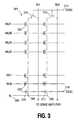
- FIG. 3illustrates a schematic diagram of a portion of a NAND architecture memory array comprising series strings of non-volatile memory cells. While the subsequent discussions refer to a NAND memory device, the present embodiments are not limited to such an architecture. Alternate embodiments can use other memory architectures with the memory controller having the DRAM expansion mode.
- the memory arrayis comprised of an array of non-volatile memory cells 301 (e.g., floating gate) arranged in columns such as series strings 304 , 305 . Each of the cells 301 are coupled drain to source in each series string 304 , 305 .
- An access linee.g. word line
- WL 0 -WL 31that spans across multiple series strings 304 , 305 is connected to the control gates of each memory cell in a row in order to bias the control gates of the memory cells in the row.
- Data linessuch as bit lines BL 1 , BL 2 are eventually connected to sense amplifiers (not shown) that detect the state of each cell by sensing current on a particular bit line.
- Each series string 304 , 305 of memory cellsis coupled to a source line 306 by a source select gate 316 , 317 and to an individual bit line BL 1 , BL 2 by a drain select gate 312 , 313 .
- the source select gates 316 , 317are controlled by a source select gate control line SG(S) 318 coupled to their control gates.
- the drain select gates 312 , 313are controlled by a drain select gate control line SG(D) 314 .
- Each memory cellcan be programmed as a single level cell (SLC) or multilevel cell (MLC).
- Each cell's threshold voltage (V t )is indicative of the data that is stored in the cell. For example, in an SLC, a V t of 0.5V might indicate a programmed cell while a V t of ⁇ 0.5V might indicate an erased cell.
- the MLCmay have multiple V t windows that each indicate a different state.
- Multilevel cellscan take advantage of the analog nature of a traditional flash cell by assigning a bit pattern to a specific voltage range stored on the cell. This technology permits the storage of two or more bits per cell, depending on the quantity of voltage ranges assigned to the cell.
- FIG. 4illustrates a functional block diagram of a non-volatile memory device 400 that can be incorporated on an integrated circuit die.
- the non-volatile memory device 400in one embodiment, is flash memory.
- the non-volatile memory device 400has been simplified to focus on features of the memory that are helpful in understanding the present programming embodiments.
- the non-volatile memory device 400includes an array 430 of non-volatile memory cells such as the floating gate memory cells that are illustrated in FIG. 3 and discussed previously.
- the memory array 430is arranged in banks of word line rows and bit line columns. In one embodiment, the columns of the memory array 430 are comprised of series strings of memory cells. As is well known in the art, the connections of the cells to the bit lines determines whether the array is a NAND architecture, an AND architecture, or a NOR architecture.
- the memory array 430can be organized into memory blocks.
- the quantity of memory blocksis typically determined by the size of the memory device (i.e., 512 MB, 1 GB). In one embodiment, each memory block is organized into 64 pages.
- Address buffer circuitry 440is provided to latch address signals provided through the I/O circuitry 460 . Address signals are received and decoded by a row decoder 444 and a column decoder 446 to access the memory array 430 . It will be appreciated by those skilled in the art, with the benefit of the present description, that the number of address input connections depends on the density and architecture of the memory array 430 . That is, the number of addresses increases with both increased memory cell counts and increased bank and block counts. Data is also input and output through the I/O circuitry 460 based on the timing of the control signals 472 .
- the non-volatile memory device 400reads data in the memory array 430 by sensing voltage or current changes in the memory array columns using sense amplifier circuitry 450 .
- the sense amplifier circuitry 450in one embodiment, is coupled to read and latch a row of data from the memory array 430 .
- Data input and output buffer circuitry 460is included for bidirectional data communication as well as address communication over a plurality of data connections 462 with an external controller.
- Write circuitry 455is provided to write data to the memory array.
- the memory control circuitry 470decodes signals provided on control bus 472 from an external controller. These signals can include read/write (R/ W ), chip enable (CE), command latch enable (CLE), address latch enable (ALE) as well as other control signals that are used to control the operations on the memory array 430 as well as other circuitry of the memory device 400 . In one embodiment, these signals are active low but alternate embodiments can use active high signals.
- the memory control circuitry 470may be a state machine, a sequencer, or some other type of controller to generate the memory control signals.
- the non-volatile memory device 400communicates with an external controller over a channel 490 .
- the channel 490is comprised of the memory address, data, and control signals between the external controller and the memory device 400 .
- the embodiment of FIG. 4shows the address and data being coupled as one bus to the I/O circuitry 460 .
- the address and data busesare separate inputs/outputs with the memory device 400 .
- FIG. 5illustrates a block diagram of one embodiment of a plurality of memory devices 501 - 508 that can make up one or more communication channels in a solid state storage device.
- This figureshows the address/data bus 510 , Read/ Write control signal 511 , and chip enable signals 512 that make up the one or more communication channels.
- the illustrated embodimentincludes eight separate memory devices so that eight chip enable signals ( CE 0 - CE 7 ) are used.
- Each memory device 501 - 508is formed on a separate die and stacked with one or more of the other memory devices to form the solid state storage device.
- a solid state storage devicemay use only one memory device 501 or multiple memory devices.
- a solid state storage devicecould be comprised of a plurality of non-volatile memory devices organized into groups of non-volatile memory devices 501 , 502 in which each group of non-volatile memory devices share a common communication channel including a single chip enable line. Each of the plurality of non-volatile memory communication channels is coupled to a different group of non-volatile memory devices.
- FIG. 6illustrates a block diagram of one embodiment of a solid state storage device controller operating in a DRAM expansion mode with two non-volatile memory channels dedicated to DRAM expansion.
- the subsequent discussionrefers to a DRAM.
- any memory device other than NAND flashcould be substituted for the DRAM and still remain within the scope of the disclosed embodiments.
- Such a memory deviceshould be capable of fast, random access and may be of a volatile or a non-volatile type.
- a slower memory devicetypically has a slower access time than the faster memory device.
- two of the controller's memory communication channels 640 , 641are instead used to communicate with an expansion DRAM bank 601 that is separate and independent from the primary DRAM bank 602 . This provides improved bandwidth as well as additional performance due to the locality of many of the DRAM operations now having twice as many DRAM pages.
- the solid state storage device memory controller 600is comprised of a memory control circuit, such as primary DRAM sequencer 621 that couples the primary DRAM device 602 to the controller 600 .
- the DRAM device 602communicates with the primary DRAM sequencer 621 over data and address/control buses 645 .
- the primary DRAM sequencer 621is a DRAM control circuit that is responsible for generating the timing and commands necessary for operation of the memory device 602 .
- the primary DRAM sequencer 621can generate the read/write control signals as well as the refresh signals necessary for proper DRAM operation.
- a secondary DRAM sequencer 620is used for essentially the same functions as the primary DRAM sequencer 621 . However, the secondary DRAM sequencer 620 is responsible for generating the control signals necessary for proper operation of the expansion DRAM device 601 .
- the non-volatile memory sequencers 630 , 631are non-volatile memory control circuits that generate the timing and commands necessary for operation of the non-volatile memory devices.
- the non-volatile memory sequencers 603control an access process to write and/or read the memory devices on each memory communication channel 650 .
- the non-volatile memory sequencers 630 , 631can generate the control signals that control the select gate drain and select gate source transistors as described with reference to FIG. 3 .
- the non-volatile memory sequencers 630 , 631may also be responsible for generating many other memory control signals.
- non-volatile memory sequencers 630 , 631are shown in FIG. 6 . Alternate embodiments may use other quantities of non-volatile memory sequencers. For example, one embodiment might use only one sequencer. Another embodiment could use a different non-volatile memory sequencer for each different memory communication channel 650 .
- the multiplexer 612in response to a select signal, is responsible for selecting which of the circuits attached to its inputs are output to the various memory communication channels 640 , 641 , 650 of the solid state storage device controller 600 .
- the select signalis generated by a CPU 610 that stores a select signal (e.g., bit or bits) in a register 611 .
- the CPU 610generates the select signal in response to data input over the host interface. For example, if an access is made by an external system to one of the memory communication channels 650 with the non-volatile memory, the CPU generates and stores a select signal that selects the appropriate channel 650 through the multiplexer 612 .
- the CPU 610If the CPU is executing an algorithm that requires updating translation tables that are stored in the expansion DRAM device 601 , the CPU 610 generates and stores a select signal that causes the multiplexer 612 to select the secondary DRAM sequencer 620 to be output so that the expansion DRAM device 601 can be accessed.
- the controller 600is additionally configured with a host interface 651 over which the controller 600 communicates with external devices/systems such as computers and cameras.
- the host interface 651can be parallel ATA, SATA, SAS, PCIe, Fiber Channel, SCSI, Gigabit Ethernet, or some other communication standard.
- the expansion DRAM device 601is coupled to the controller 600 over two of the communication channels 640 , 641 that are normally used for communication with the non-volatile memory devices.
- the two channels 640 , 641are coupled to the address/command bus 640 and the data bus 641 of the DRAM device 601 .
- the expansion DRAM device 601is used to store additional translation tables and for additional data buffering.
- Typical uses for the primary DRAM and the expansion DRAMinclude: transfer from non-volatile memory to DRAM during a solid state storage device read operation, transfer from DRAM to non-volatile memory on a solid state storage device write operation, error correction operations on read data, translation table read (allowing a logical drive address to map to any physical non-volatile memory address), data collection read operation from non-volatile memory, data collection write operation to non-volatile memory, static wear-leveling, translation table update due to data collection operations or static wear-leveling, and translation table write operations to non-volatile memory.
- the above-described elements of the solid state storage device memory controller of FIG. 6are a logical representation of the functions performed by the controller. These elements are not necessarily required for proper operation of the controller. Alternate embodiments may use other elements to perform substantially the same functions. Additionally, for purposes of clarity, not all elements of the memory controller are shown. Only those elements related to proper operation of the disclosed embodiments are shown and discussed.
- FIG. 7illustrates two memory address maps for use with the embodiment of FIG. 6 .
- This memory mapshows how the DRAM addresses are split between the two DRAM devices 601 , 602 of FIG. 6 . These addresses are generated by the primary sequencer 621 and secondary sequencer 620 in combination with the CPU 610 of the controller 600 .
- FIG. 7shows that if the controller 600 is not in the DRAM expansion mode, only the single primary DRAM device 602 is used.
- the memory map for the primary DRAM device 602is in the range of 00000000H to 70000000H (32 address bits).
- the addresses 00000000H to 7FFFFFFFHare used to address the primary DRAM 602 while 80000000H to FFFFFFH are used to address the expansion DRAM device 601 .
- the address maps of FIG. 7are for purposes of illustration only. If different size primary and/or expansion DRAM devices are used, the address map will be comprised of different addresses. Also, the addresses for each DRAM can start in different locations than 00000000H or 80000000H.
- FIG. 8illustrates an alternate embodiment of a solid state storage device controller 800 having a DRAM expansion mode with a single non-volatile memory channel 811 dedicated to DRAM expansion.
- the width of the communication channel 811 for the expansion DRAMis sufficient to expand the data bus to a width of 32 bits.
- the solid state storage device controller 800 of FIG. 8is comprised of a DRAM sequencer 803 that is responsible for generating the control signals for both the primary DRAM device 801 and the expansion DRAM device 802 . As discussed previously, the sequencer 803 generates the necessary read, write, and refresh control signals for proper operation of a DRAM device.
- a non-volatile memory sequencer 804generates the non-volatile memory control signals to write and/or read the memory devices on each memory communications channel 810 that is coupled to at least one non-volatile memory device.
- the non-volatile memory sequencer 804can generate the control signals that control the select gate drain and select gate source transistors as described with reference to FIG. 3 .
- the non-volatile memory sequencer 804may also be responsible for generating many other non-volatile memory control signals.
- Both the DRAM sequencer 803 and the non-volatile memory sequencer 804are input to a multiplexer 805 that selects between the two sequencers 803 , 804 in response to the select signal.
- the CPU 807generates the select signal that is then stored in the register 806 . If an input data signal is to be stored in one of the non-volatile memories coupled to one of the non-volatile memory communication channels 810 , the CPU 807 generates a select signal that selects the non-volatile memory sequencer 804 to be output by the multiplexer 805 . If the CPU 807 requires the use of the expansion DRAM, the CPU 807 generates the select signal that selects the memory communication channel (e.g., Channel 10 ) 811 that is coupled to the expansion DRAM data bus.
- the memory communication channele.g., Channel 10
- both DRAM devices 801 , 802are exposed to the same addresses and commands.
- Each DRAMwould have a write mask that enabled it to differentiate between addresses and commands meant for the other device 801 , 802 .
- This embodimentcould also use data steering logic (not shown) to take advantage of the wider data bus.
- the least significant address bitwould then be used to select the upper or lower 16-bit portions of the DRAM data bus.
- the remaining address bits coming into the DRAM sequencerwould be shifted down one.
- the above-described elements of the solid state storage device memory controller of FIG. 8are a logical representation of the functions performed by the controller. These elements are not necessarily required for proper operation of the controller. Alternate embodiments may use other elements to perform substantially the same functions. Additionally, for purposes of clarity, not all elements of the memory controller are shown. Only those elements related to proper operation of the disclosed embodiments are shown and discussed.
- FIG. 9illustrates DRAM address maps in accordance with the embodiment of FIG. 8 .
- the controller 800is in the 16-bit mode so that addresses 0000H to FFFFH are used. If the controller is in the DRAM expansion mode, the addresses in the primary DRAM device use even addresses 00000000H to FFFFFFFEH while the expansion DRAM device uses odd addresses 00000001H to FFFFFFFFH.
- the address maps of FIG. 9are for purposes of illustration only. If different size primary and/or expansion DRAM devices are used, the address maps will be comprised of different addresses. Also, the addresses for each DRAM can start in different locations than 00000000H.
- FIG. 10illustrates a logical block diagram of the embodiment of FIG. 6 but operating in the non-expansion mode (e.g., the non-volatile memory mode) instead of the expansion mode as illustrated in FIG. 6 .
- the non-expansion modee.g., the non-volatile memory mode
- FIG. 10illustrates a logical block diagram of the embodiment of FIG. 6 but operating in the non-expansion mode (e.g., the non-volatile memory mode) instead of the expansion mode as illustrated in FIG. 6 .
- the non-expansion modee.g., the non-volatile memory mode
- the communication channels 650are dedicated only to the non-volatile memory devices of each channel.
- the secondary DRAM sequencer 620is still present but is not being used without the extra expansion DRAM installed.
- the selection of the different modesfor the above-described embodiments can be performed by a hardwired mode selection input 1000 for the solid state storage device controller as illustrated in FIG. 10 .
- the mode selectionmay be done during manufacture of the solid state storage device with a jumper to ground for one mode and a jumper to VCC for the other mode. This allows the manufacturer to make and inventory only one controller that is capable of operating in both modes.
- the modecan be selected by a command from the CPU in the controller. The CPU may detect the presence of a DRAM and configure the ports appropriately.
- FIG. 11illustrates a flowchart of one embodiment of a method of operation of a solid state storage device controller with a DRAM expansion mode.
- the expansion modeis enabled 1101 either through the hardwired input or the command from a CPU in the controller.
- the controllerthen communicates with the expansion DRAM over one or more of the memory communication channels 1103 as described in the embodiments above.
- one or more embodimentsprovide a solid state storage device controller with the capability to operate in both an expansion mode and a non-expansion memory mode.
- the expansion modeuses one or more memory communication channels, normally used for non-volatile memory communication, to communicate with an expansion DRAM device.
- the solid state storage devicecould be a solid state drive (SSD) used in computers to replace the magnetic hard drive.
Landscapes
- Engineering & Computer Science (AREA)
- Theoretical Computer Science (AREA)
- Physics & Mathematics (AREA)
- General Engineering & Computer Science (AREA)
- General Physics & Mathematics (AREA)
- Human Computer Interaction (AREA)
- Dram (AREA)
- Computer And Data Communications (AREA)
Abstract
Description
Claims (15)
Priority Applications (10)
| Application Number | Priority Date | Filing Date | Title |
|---|---|---|---|
| US12/241,794US8069300B2 (en) | 2008-09-30 | 2008-09-30 | Solid state storage device controller with expansion mode |
| EP16020283.4AEP3121704B1 (en) | 2008-09-30 | 2009-09-03 | Solid state storage device controller with expansion mode |
| PCT/US2009/055859WO2010039390A2 (en) | 2008-09-30 | 2009-09-03 | Solid state storage device controller with expansion mode |
| KR1020117009805AKR101265423B1 (en) | 2008-09-30 | 2009-09-03 | Solid state storage device controller with expansion mode |
| CN200980138496.6ACN102165409B (en) | 2008-09-30 | 2009-09-03 | Solid state storage device controller with expansion mode |
| EP09818196.9AEP2332036B1 (en) | 2008-09-30 | 2009-09-03 | Solid state storage device controller with expansion mode |
| TW098131273ATWI434286B (en) | 2008-09-30 | 2009-09-16 | Solid state storage device controller with expansion mode and method for operation of the same |
| US13/293,321US8200894B2 (en) | 2008-09-30 | 2011-11-10 | Solid state storage device controller with expansion mode |
| US13/482,517US8452916B2 (en) | 2008-09-30 | 2012-05-29 | Solid state storage device controller with expansion mode |
| US13/901,806US8832360B2 (en) | 2008-09-30 | 2013-05-24 | Solid state storage device controller with expansion mode |
Applications Claiming Priority (1)
| Application Number | Priority Date | Filing Date | Title |
|---|---|---|---|
| US12/241,794US8069300B2 (en) | 2008-09-30 | 2008-09-30 | Solid state storage device controller with expansion mode |
Related Child Applications (1)
| Application Number | Title | Priority Date | Filing Date |
|---|---|---|---|
| US13/293,321DivisionUS8200894B2 (en) | 2008-09-30 | 2011-11-10 | Solid state storage device controller with expansion mode |
Publications (2)
| Publication Number | Publication Date |
|---|---|
| US20100082881A1 US20100082881A1 (en) | 2010-04-01 |
| US8069300B2true US8069300B2 (en) | 2011-11-29 |
Family
ID=42058808
Family Applications (4)
| Application Number | Title | Priority Date | Filing Date |
|---|---|---|---|
| US12/241,794Active2030-07-31US8069300B2 (en) | 2008-09-30 | 2008-09-30 | Solid state storage device controller with expansion mode |
| US13/293,321ActiveUS8200894B2 (en) | 2008-09-30 | 2011-11-10 | Solid state storage device controller with expansion mode |
| US13/482,517ActiveUS8452916B2 (en) | 2008-09-30 | 2012-05-29 | Solid state storage device controller with expansion mode |
| US13/901,806ActiveUS8832360B2 (en) | 2008-09-30 | 2013-05-24 | Solid state storage device controller with expansion mode |
Family Applications After (3)
| Application Number | Title | Priority Date | Filing Date |
|---|---|---|---|
| US13/293,321ActiveUS8200894B2 (en) | 2008-09-30 | 2011-11-10 | Solid state storage device controller with expansion mode |
| US13/482,517ActiveUS8452916B2 (en) | 2008-09-30 | 2012-05-29 | Solid state storage device controller with expansion mode |
| US13/901,806ActiveUS8832360B2 (en) | 2008-09-30 | 2013-05-24 | Solid state storage device controller with expansion mode |
Country Status (6)
| Country | Link |
|---|---|
| US (4) | US8069300B2 (en) |
| EP (2) | EP2332036B1 (en) |
| KR (1) | KR101265423B1 (en) |
| CN (1) | CN102165409B (en) |
| TW (1) | TWI434286B (en) |
| WO (1) | WO2010039390A2 (en) |
Cited By (2)
| Publication number | Priority date | Publication date | Assignee | Title |
|---|---|---|---|---|
| US20120246525A1 (en)* | 2011-03-21 | 2012-09-27 | Denso Corporation | Method for initiating a refresh operation in a solid-state nonvolatile memory device |
| US9589614B2 (en) | 2014-10-28 | 2017-03-07 | Samsung Electronics Co., Ltd. | Multi-chip memory system having chip enable function |
Families Citing this family (35)
| Publication number | Priority date | Publication date | Assignee | Title |
|---|---|---|---|---|
| US8432732B2 (en)* | 2010-07-09 | 2013-04-30 | Sandisk Technologies Inc. | Detection of word-line leakage in memory arrays |
| US8514630B2 (en) | 2010-07-09 | 2013-08-20 | Sandisk Technologies Inc. | Detection of word-line leakage in memory arrays: current based approach |
| US8305807B2 (en) | 2010-07-09 | 2012-11-06 | Sandisk Technologies Inc. | Detection of broken word-lines in memory arrays |
| US20120110244A1 (en)* | 2010-11-02 | 2012-05-03 | Micron Technology, Inc. | Copyback operations |
| US8379454B2 (en) | 2011-05-05 | 2013-02-19 | Sandisk Technologies Inc. | Detection of broken word-lines in memory arrays |
| US8775901B2 (en) | 2011-07-28 | 2014-07-08 | SanDisk Technologies, Inc. | Data recovery for defective word lines during programming of non-volatile memory arrays |
| US8750042B2 (en) | 2011-07-28 | 2014-06-10 | Sandisk Technologies Inc. | Combined simultaneous sensing of multiple wordlines in a post-write read (PWR) and detection of NAND failures |
| CN102566943B (en)* | 2011-12-31 | 2015-03-11 | 记忆科技(深圳)有限公司 | Solid state disk and communication method based on solid state disk |
| US8730722B2 (en) | 2012-03-02 | 2014-05-20 | Sandisk Technologies Inc. | Saving of data in cases of word-line to word-line short in memory arrays |
| US9342259B2 (en)* | 2012-09-10 | 2016-05-17 | Texas Instruments Incorporated | Nonvolatile logic array and power domain segmentation in processing device |
| US9471484B2 (en) | 2012-09-19 | 2016-10-18 | Novachips Canada Inc. | Flash memory controller having dual mode pin-out |
| US9810723B2 (en) | 2012-09-27 | 2017-11-07 | Sandisk Technologies Llc | Charge pump based over-sampling ADC for current detection |
| US9164526B2 (en) | 2012-09-27 | 2015-10-20 | Sandisk Technologies Inc. | Sigma delta over-sampling charge pump analog-to-digital converter |
| US9098402B2 (en) | 2012-12-21 | 2015-08-04 | Intel Corporation | Techniques to configure a solid state drive to operate in a storage mode or a memory mode |
| US9280497B2 (en) | 2012-12-21 | 2016-03-08 | Dell Products Lp | Systems and methods for support of non-volatile memory on a DDR memory channel |
| US9921980B2 (en) | 2013-08-12 | 2018-03-20 | Micron Technology, Inc. | Apparatuses and methods for configuring I/Os of memory for hybrid memory modules |
| US9165683B2 (en) | 2013-09-23 | 2015-10-20 | Sandisk Technologies Inc. | Multi-word line erratic programming detection |
| US20150205541A1 (en)* | 2014-01-20 | 2015-07-23 | Samya Systems, Inc. | High-capacity solid state disk drives |
| US10521387B2 (en)* | 2014-02-07 | 2019-12-31 | Toshiba Memory Corporation | NAND switch |
| US9484086B2 (en) | 2014-07-10 | 2016-11-01 | Sandisk Technologies Llc | Determination of word line to local source line shorts |
| US9443612B2 (en) | 2014-07-10 | 2016-09-13 | Sandisk Technologies Llc | Determination of bit line to low voltage signal shorts |
| US9460809B2 (en) | 2014-07-10 | 2016-10-04 | Sandisk Technologies Llc | AC stress mode to screen out word line to word line shorts |
| US9514835B2 (en) | 2014-07-10 | 2016-12-06 | Sandisk Technologies Llc | Determination of word line to word line shorts between adjacent blocks |
| US9823846B2 (en)* | 2014-08-20 | 2017-11-21 | Qualcomm Incorporated | Systems and methods for expanding memory for a system on chip |
| US9202593B1 (en) | 2014-09-02 | 2015-12-01 | Sandisk Technologies Inc. | Techniques for detecting broken word lines in non-volatile memories |
| US9240249B1 (en) | 2014-09-02 | 2016-01-19 | Sandisk Technologies Inc. | AC stress methods to screen out bit line defects |
| US9449694B2 (en) | 2014-09-04 | 2016-09-20 | Sandisk Technologies Llc | Non-volatile memory with multi-word line select for defect detection operations |
| US10007435B2 (en) | 2015-05-21 | 2018-06-26 | Micron Technology, Inc. | Translation lookaside buffer in memory |
| US9697320B2 (en)* | 2015-09-24 | 2017-07-04 | Qualcomm Incorporated | Rectilinear macros having non-uniform channel spacing |
| US9698676B1 (en) | 2016-03-11 | 2017-07-04 | Sandisk Technologies Llc | Charge pump based over-sampling with uniform step size for current detection |
| JP6753746B2 (en)* | 2016-09-15 | 2020-09-09 | キオクシア株式会社 | Semiconductor memory device |
| CN106598742B (en)* | 2016-12-26 | 2020-01-03 | 湖南国科微电子股份有限公司 | SSD master control internal load balancing system and method |
| US10628049B2 (en) | 2017-07-12 | 2020-04-21 | Sandisk Technologies Llc | Systems and methods for on-die control of memory command, timing, and/or control signals |
| US10783953B2 (en)* | 2017-12-04 | 2020-09-22 | Advanced Micro Devices, Inc. | Memory with expandable row width |
| US10802750B2 (en)* | 2019-02-28 | 2020-10-13 | Silicon Motion Inc. | Universal flash storage memory module, controller and electronic device with advanced turbo write buffer and method for operating the memory module |
Citations (7)
| Publication number | Priority date | Publication date | Assignee | Title |
|---|---|---|---|---|
| US20040024916A1 (en) | 2002-07-30 | 2004-02-05 | Chien Hsing | Portable computer with shared expansion slot |
| US20060190642A1 (en) | 2005-02-24 | 2006-08-24 | International Business Machines Corporation | Method and apparatus for testing, characterizing and monitoring a chip interface using a second data path |
| US20070245076A1 (en)* | 2006-04-12 | 2007-10-18 | Giga-Byte Technology Co., Ltd. | Volatile storage device and serial mixed storage system having the same |
| US20080082731A1 (en) | 2006-09-28 | 2008-04-03 | Vijay Karamcheti | Main memory in a system with a memory controller configured to control access to non-volatile memory, and related technologies |
| WO2008086488A2 (en) | 2007-01-10 | 2008-07-17 | Mobile Semiconductor Corporation | Adaptive memory system for enhancing the performance of an external computing device |
| US20090063757A1 (en)* | 2007-08-30 | 2009-03-05 | Unity Semiconductor Corporation | Memory emulation in an electronic organizer |
| US20090164722A1 (en)* | 2007-12-24 | 2009-06-25 | Samsung Electronics Co., Ltd. | Memory card and memory storage device using the same |
Family Cites Families (8)
| Publication number | Priority date | Publication date | Assignee | Title |
|---|---|---|---|---|
| JP3289661B2 (en)* | 1997-11-07 | 2002-06-10 | 日本電気株式会社 | Cache memory system |
| US8452912B2 (en)* | 2007-10-11 | 2013-05-28 | Super Talent Electronics, Inc. | Flash-memory system with enhanced smart-storage switch and packed meta-data cache for mitigating write amplification by delaying and merging writes until a host read |
| JP4722305B2 (en)* | 2001-02-27 | 2011-07-13 | 富士通セミコンダクター株式会社 | Memory system |
| JP4499982B2 (en)* | 2002-09-11 | 2010-07-14 | 株式会社日立製作所 | Memory system |
| KR100704037B1 (en) | 2005-04-15 | 2007-04-04 | 삼성전자주식회사 | Data storage device having heterogeneous nonvolatile memory and its driving method |
| CN100464290C (en)* | 2007-09-10 | 2009-02-25 | 杭州华三通信技术有限公司 | cache management system |
| US8185685B2 (en)* | 2007-12-14 | 2012-05-22 | Hitachi Global Storage Technologies Netherlands B.V. | NAND flash module replacement for DRAM module |
| US8359423B2 (en)* | 2008-03-14 | 2013-01-22 | Spansion Llc | Using LPDDR1 bus as transport layer to communicate to flash |
- 2008
- 2008-09-30USUS12/241,794patent/US8069300B2/enactiveActive
- 2009
- 2009-09-03WOPCT/US2009/055859patent/WO2010039390A2/enactiveApplication Filing
- 2009-09-03EPEP09818196.9Apatent/EP2332036B1/enactiveActive
- 2009-09-03KRKR1020117009805Apatent/KR101265423B1/enactiveActive
- 2009-09-03EPEP16020283.4Apatent/EP3121704B1/enactiveActive
- 2009-09-03CNCN200980138496.6Apatent/CN102165409B/enactiveActive
- 2009-09-16TWTW098131273Apatent/TWI434286B/enactive
- 2011
- 2011-11-10USUS13/293,321patent/US8200894B2/enactiveActive
- 2012
- 2012-05-29USUS13/482,517patent/US8452916B2/enactiveActive
- 2013
- 2013-05-24USUS13/901,806patent/US8832360B2/enactiveActive
Patent Citations (8)
| Publication number | Priority date | Publication date | Assignee | Title |
|---|---|---|---|---|
| US20040024916A1 (en) | 2002-07-30 | 2004-02-05 | Chien Hsing | Portable computer with shared expansion slot |
| US20060190642A1 (en) | 2005-02-24 | 2006-08-24 | International Business Machines Corporation | Method and apparatus for testing, characterizing and monitoring a chip interface using a second data path |
| US20070245076A1 (en)* | 2006-04-12 | 2007-10-18 | Giga-Byte Technology Co., Ltd. | Volatile storage device and serial mixed storage system having the same |
| US20080082731A1 (en) | 2006-09-28 | 2008-04-03 | Vijay Karamcheti | Main memory in a system with a memory controller configured to control access to non-volatile memory, and related technologies |
| WO2008086488A2 (en) | 2007-01-10 | 2008-07-17 | Mobile Semiconductor Corporation | Adaptive memory system for enhancing the performance of an external computing device |
| US20090024819A1 (en)* | 2007-01-10 | 2009-01-22 | Mobile Semiconductor Corporation | Adaptive memory system for enhancing the performance of an external computing device |
| US20090063757A1 (en)* | 2007-08-30 | 2009-03-05 | Unity Semiconductor Corporation | Memory emulation in an electronic organizer |
| US20090164722A1 (en)* | 2007-12-24 | 2009-06-25 | Samsung Electronics Co., Ltd. | Memory card and memory storage device using the same |
Cited By (3)
| Publication number | Priority date | Publication date | Assignee | Title |
|---|---|---|---|---|
| US20120246525A1 (en)* | 2011-03-21 | 2012-09-27 | Denso Corporation | Method for initiating a refresh operation in a solid-state nonvolatile memory device |
| US8756474B2 (en)* | 2011-03-21 | 2014-06-17 | Denso International America, Inc. | Method for initiating a refresh operation in a solid-state nonvolatile memory device |
| US9589614B2 (en) | 2014-10-28 | 2017-03-07 | Samsung Electronics Co., Ltd. | Multi-chip memory system having chip enable function |
Also Published As
| Publication number | Publication date |
|---|---|
| EP3121704A1 (en) | 2017-01-25 |
| EP2332036A2 (en) | 2011-06-15 |
| US20140013035A1 (en) | 2014-01-09 |
| TWI434286B (en) | 2014-04-11 |
| US8200894B2 (en) | 2012-06-12 |
| US20120059980A1 (en) | 2012-03-08 |
| EP2332036A4 (en) | 2014-10-29 |
| EP2332036B1 (en) | 2016-10-26 |
| US8452916B2 (en) | 2013-05-28 |
| KR20110063580A (en) | 2011-06-10 |
| EP3121704B1 (en) | 2018-01-17 |
| CN102165409A (en) | 2011-08-24 |
| KR101265423B1 (en) | 2013-05-16 |
| US20100082881A1 (en) | 2010-04-01 |
| WO2010039390A2 (en) | 2010-04-08 |
| TW201017679A (en) | 2010-05-01 |
| CN102165409B (en) | 2014-10-01 |
| US8832360B2 (en) | 2014-09-09 |
| WO2010039390A3 (en) | 2010-05-27 |
| US20120233392A1 (en) | 2012-09-13 |
Similar Documents
| Publication | Publication Date | Title |
|---|---|---|
| US8069300B2 (en) | Solid state storage device controller with expansion mode | |
| US9418017B2 (en) | Hot memory block table in a solid state storage device | |
| US9405679B2 (en) | Determining a location of a memory device in a solid state device | |
| US8244937B2 (en) | Solid state storage device controller with parallel operation mode | |
| US20180211707A1 (en) | Semiconductor memory device and method of controlling semiconductor memory device |
Legal Events
| Date | Code | Title | Description |
|---|---|---|---|
| AS | Assignment | Owner name:MICRON TECHNOLOGY, INC.,IDAHO Free format text:ASSIGNMENT OF ASSIGNORS INTEREST;ASSIGNOR:KLEIN, DEAN;REEL/FRAME:021609/0510 Effective date:20080924 Owner name:MICRON TECHNOLOGY, INC., IDAHO Free format text:ASSIGNMENT OF ASSIGNORS INTEREST;ASSIGNOR:KLEIN, DEAN;REEL/FRAME:021609/0510 Effective date:20080924 | |
| FEPP | Fee payment procedure | Free format text:PAYOR NUMBER ASSIGNED (ORIGINAL EVENT CODE: ASPN); ENTITY STATUS OF PATENT OWNER: LARGE ENTITY | |
| STCF | Information on status: patent grant | Free format text:PATENTED CASE | |
| FPAY | Fee payment | Year of fee payment:4 | |
| AS | Assignment | Owner name:U.S. BANK NATIONAL ASSOCIATION, AS COLLATERAL AGENT, CALIFORNIA Free format text:SECURITY INTEREST;ASSIGNOR:MICRON TECHNOLOGY, INC.;REEL/FRAME:038669/0001 Effective date:20160426 Owner name:U.S. BANK NATIONAL ASSOCIATION, AS COLLATERAL AGEN Free format text:SECURITY INTEREST;ASSIGNOR:MICRON TECHNOLOGY, INC.;REEL/FRAME:038669/0001 Effective date:20160426 | |
| AS | Assignment | Owner name:MORGAN STANLEY SENIOR FUNDING, INC., AS COLLATERAL AGENT, MARYLAND Free format text:PATENT SECURITY AGREEMENT;ASSIGNOR:MICRON TECHNOLOGY, INC.;REEL/FRAME:038954/0001 Effective date:20160426 Owner name:MORGAN STANLEY SENIOR FUNDING, INC., AS COLLATERAL Free format text:PATENT SECURITY AGREEMENT;ASSIGNOR:MICRON TECHNOLOGY, INC.;REEL/FRAME:038954/0001 Effective date:20160426 | |
| AS | Assignment | Owner name:U.S. BANK NATIONAL ASSOCIATION, AS COLLATERAL AGENT, CALIFORNIA Free format text:CORRECTIVE ASSIGNMENT TO CORRECT THE REPLACE ERRONEOUSLY FILED PATENT #7358718 WITH THE CORRECT PATENT #7358178 PREVIOUSLY RECORDED ON REEL 038669 FRAME 0001. ASSIGNOR(S) HEREBY CONFIRMS THE SECURITY INTEREST;ASSIGNOR:MICRON TECHNOLOGY, INC.;REEL/FRAME:043079/0001 Effective date:20160426 Owner name:U.S. BANK NATIONAL ASSOCIATION, AS COLLATERAL AGEN Free format text:CORRECTIVE ASSIGNMENT TO CORRECT THE REPLACE ERRONEOUSLY FILED PATENT #7358718 WITH THE CORRECT PATENT #7358178 PREVIOUSLY RECORDED ON REEL 038669 FRAME 0001. ASSIGNOR(S) HEREBY CONFIRMS THE SECURITY INTEREST;ASSIGNOR:MICRON TECHNOLOGY, INC.;REEL/FRAME:043079/0001 Effective date:20160426 | |
| AS | Assignment | Owner name:JPMORGAN CHASE BANK, N.A., AS COLLATERAL AGENT, ILLINOIS Free format text:SECURITY INTEREST;ASSIGNORS:MICRON TECHNOLOGY, INC.;MICRON SEMICONDUCTOR PRODUCTS, INC.;REEL/FRAME:047540/0001 Effective date:20180703 Owner name:JPMORGAN CHASE BANK, N.A., AS COLLATERAL AGENT, IL Free format text:SECURITY INTEREST;ASSIGNORS:MICRON TECHNOLOGY, INC.;MICRON SEMICONDUCTOR PRODUCTS, INC.;REEL/FRAME:047540/0001 Effective date:20180703 | |
| AS | Assignment | Owner name:MICRON TECHNOLOGY, INC., IDAHO Free format text:RELEASE BY SECURED PARTY;ASSIGNOR:U.S. BANK NATIONAL ASSOCIATION, AS COLLATERAL AGENT;REEL/FRAME:047243/0001 Effective date:20180629 | |
| MAFP | Maintenance fee payment | Free format text:PAYMENT OF MAINTENANCE FEE, 8TH YEAR, LARGE ENTITY (ORIGINAL EVENT CODE: M1552); ENTITY STATUS OF PATENT OWNER: LARGE ENTITY Year of fee payment:8 | |
| AS | Assignment | Owner name:MICRON TECHNOLOGY, INC., IDAHO Free format text:RELEASE BY SECURED PARTY;ASSIGNOR:MORGAN STANLEY SENIOR FUNDING, INC., AS COLLATERAL AGENT;REEL/FRAME:050937/0001 Effective date:20190731 | |
| AS | Assignment | Owner name:MICRON SEMICONDUCTOR PRODUCTS, INC., IDAHO Free format text:RELEASE BY SECURED PARTY;ASSIGNOR:JPMORGAN CHASE BANK, N.A., AS COLLATERAL AGENT;REEL/FRAME:051028/0001 Effective date:20190731 Owner name:MICRON TECHNOLOGY, INC., IDAHO Free format text:RELEASE BY SECURED PARTY;ASSIGNOR:JPMORGAN CHASE BANK, N.A., AS COLLATERAL AGENT;REEL/FRAME:051028/0001 Effective date:20190731 | |
| MAFP | Maintenance fee payment | Free format text:PAYMENT OF MAINTENANCE FEE, 12TH YEAR, LARGE ENTITY (ORIGINAL EVENT CODE: M1553); ENTITY STATUS OF PATENT OWNER: LARGE ENTITY Year of fee payment:12 |