US8067308B2 - Semiconductor device and method of forming an interconnect structure with TSV using encapsulant for structural support - Google Patents
Semiconductor device and method of forming an interconnect structure with TSV using encapsulant for structural supportDownload PDFInfo
- Publication number
- US8067308B2 US8067308B2US12/480,317US48031709AUS8067308B2US 8067308 B2US8067308 B2US 8067308B2US 48031709 AUS48031709 AUS 48031709AUS 8067308 B2US8067308 B2US 8067308B2
- Authority
- US
- United States
- Prior art keywords
- forming
- conductive
- substrate
- interconnect structure
- conductive layer
- Prior art date
- Legal status (The legal status is an assumption and is not a legal conclusion. Google has not performed a legal analysis and makes no representation as to the accuracy of the status listed.)
- Active
Links
- 239000004065semiconductorSubstances0.000titleclaimsabstractdescription162
- 239000008393encapsulating agentSubstances0.000titleclaimsabstractdescription36
- 238000000034methodMethods0.000titledescription50
- 239000000758substrateSubstances0.000claimsabstractdescription89
- 238000004519manufacturing processMethods0.000claimsdescription47
- 239000004020conductorSubstances0.000claimsdescription33
- 238000000151depositionMethods0.000claimsdescription17
- 229910052710siliconInorganic materials0.000claimsdescription9
- 239000010703siliconSubstances0.000claimsdescription9
- 230000008569processEffects0.000description41
- 239000000463materialSubstances0.000description32
- 235000012431wafersNutrition0.000description29
- 239000010949copperSubstances0.000description17
- HCWZEPKLWVAEOV-UHFFFAOYSA-N2,2',5,5'-tetrachlorobiphenylChemical compoundClC1=CC=C(Cl)C(C=2C(=CC=C(Cl)C=2)Cl)=C1HCWZEPKLWVAEOV-UHFFFAOYSA-N0.000description16
- VYPSYNLAJGMNEJ-UHFFFAOYSA-NSilicium dioxideChemical compoundO=[Si]=OVYPSYNLAJGMNEJ-UHFFFAOYSA-N0.000description16
- 238000005229chemical vapour depositionMethods0.000description16
- 238000005240physical vapour depositionMethods0.000description16
- PXHVJJICTQNCMI-UHFFFAOYSA-NNickelChemical compound[Ni]PXHVJJICTQNCMI-UHFFFAOYSA-N0.000description15
- 241000724291Tobacco streak virusSpecies0.000description15
- 238000009713electroplatingMethods0.000description15
- 239000011135tinSubstances0.000description15
- 238000007772electroless platingMethods0.000description14
- 239000010931goldSubstances0.000description14
- 229910000679solderInorganic materials0.000description14
- 229910052802copperInorganic materials0.000description13
- 229910052737goldInorganic materials0.000description13
- 229910052782aluminiumInorganic materials0.000description12
- 229910052759nickelInorganic materials0.000description12
- 238000004806packaging method and processMethods0.000description12
- 230000006870functionEffects0.000description11
- 229910052718tinInorganic materials0.000description11
- 239000011133leadSubstances0.000description10
- 238000001465metallisationMethods0.000description10
- 229920002120photoresistant polymerPolymers0.000description10
- 229910052709silverInorganic materials0.000description10
- 239000010944silver (metal)Substances0.000description9
- 229910052581Si3N4Inorganic materials0.000description8
- XUIMIQQOPSSXEZ-UHFFFAOYSA-NSiliconChemical compound[Si]XUIMIQQOPSSXEZ-UHFFFAOYSA-N0.000description8
- 230000003647oxidationEffects0.000description8
- 238000007254oxidation reactionMethods0.000description8
- BPUBBGLMJRNUCC-UHFFFAOYSA-Noxygen(2-);tantalum(5+)Chemical compound[O-2].[O-2].[O-2].[O-2].[O-2].[Ta+5].[Ta+5]BPUBBGLMJRNUCC-UHFFFAOYSA-N0.000description8
- 235000012239silicon dioxideNutrition0.000description8
- 239000000377silicon dioxideSubstances0.000description8
- HQVNEWCFYHHQES-UHFFFAOYSA-Nsilicon nitrideChemical compoundN12[Si]34N5[Si]62N3[Si]51N64HQVNEWCFYHHQES-UHFFFAOYSA-N0.000description8
- PBCFLUZVCVVTBY-UHFFFAOYSA-Ntantalum pentoxideInorganic materialsO=[Ta](=O)O[Ta](=O)=OPBCFLUZVCVVTBY-UHFFFAOYSA-N0.000description8
- PNEYBMLMFCGWSK-UHFFFAOYSA-Naluminium oxideInorganic materials[O-2].[O-2].[O-2].[Al+3].[Al+3]PNEYBMLMFCGWSK-UHFFFAOYSA-N0.000description7
- 239000003990capacitorSubstances0.000description7
- 229910052593corundumInorganic materials0.000description7
- 238000005530etchingMethods0.000description7
- 238000007639printingMethods0.000description7
- 238000012545processingMethods0.000description7
- 238000004544sputter depositionMethods0.000description7
- 229910001845yogo sapphireInorganic materials0.000description7
- -1SiONChemical compound0.000description6
- 230000015572biosynthetic processEffects0.000description6
- 238000002161passivationMethods0.000description6
- 238000005245sinteringMethods0.000description6
- 238000004528spin coatingMethods0.000description6
- 238000005507sprayingMethods0.000description6
- 230000004888barrier functionEffects0.000description5
- 238000002955isolationMethods0.000description5
- 238000000465mouldingMethods0.000description5
- 229920000642polymerPolymers0.000description5
- 238000013461designMethods0.000description4
- 230000005684electric fieldEffects0.000description4
- 230000005496eutecticsEffects0.000description4
- 230000008020evaporationEffects0.000description4
- 238000001704evaporationMethods0.000description4
- 238000000227grindingMethods0.000description4
- 238000007650screen-printingMethods0.000description4
- PITHIPNORFGJPI-UHFFFAOYSA-N1,2,3-trichloro-5-(2,4,6-trichlorophenyl)benzeneChemical compoundClC1=CC(Cl)=CC(Cl)=C1C1=CC(Cl)=C(Cl)C(Cl)=C1PITHIPNORFGJPI-UHFFFAOYSA-N0.000description3
- MMTJWDQKGUNSDK-UHFFFAOYSA-N1,2,4,5-tetrachloro-3-(2,4,6-trichlorophenyl)benzeneChemical compoundClC1=CC(Cl)=CC(Cl)=C1C1=C(Cl)C(Cl)=CC(Cl)=C1ClMMTJWDQKGUNSDK-UHFFFAOYSA-N0.000description3
- 208000024875Infantile dystonia-parkinsonismDiseases0.000description3
- KDLHZDBZIXYQEI-UHFFFAOYSA-NPalladiumChemical compound[Pd]KDLHZDBZIXYQEI-UHFFFAOYSA-N0.000description3
- 229910052797bismuthInorganic materials0.000description3
- 238000004891communicationMethods0.000description3
- 230000006835compressionEffects0.000description3
- 238000007906compressionMethods0.000description3
- 230000008021depositionEffects0.000description3
- 238000009792diffusion processMethods0.000description3
- 230000007613environmental effectEffects0.000description3
- 230000004907fluxEffects0.000description3
- 238000010438heat treatmentMethods0.000description3
- 208000001543infantile parkinsonism-dystoniaDiseases0.000description3
- 229910052745leadInorganic materials0.000description3
- 230000008018meltingEffects0.000description3
- 238000002844meltingMethods0.000description3
- HBVFXTAPOLSOPB-UHFFFAOYSA-Nnickel vanadiumChemical compound[V].[Ni]HBVFXTAPOLSOPB-UHFFFAOYSA-N0.000description3
- 238000000206photolithographyMethods0.000description3
- 238000001020plasma etchingMethods0.000description3
- BASFCYQUMIYNBI-UHFFFAOYSA-NplatinumChemical compound[Pt]BASFCYQUMIYNBI-UHFFFAOYSA-N0.000description3
- 238000005498polishingMethods0.000description3
- 239000004593EpoxySubstances0.000description2
- 229920009638Tetrafluoroethylene-Hexafluoropropylene-Vinylidenefluoride CopolymerPolymers0.000description2
- 241000403254Turkey hepatitis virusSpecies0.000description2
- 230000009471actionEffects0.000description2
- 239000000853adhesiveSubstances0.000description2
- 230000001070adhesive effectEffects0.000description2
- UMIVXZPTRXBADB-UHFFFAOYSA-NbenzocyclobuteneChemical compoundC1=CC=C2CCC2=C1UMIVXZPTRXBADB-UHFFFAOYSA-N0.000description2
- 239000000919ceramicSubstances0.000description2
- 239000011651chromiumSubstances0.000description2
- 239000002131composite materialSubstances0.000description2
- 150000001875compoundsChemical class0.000description2
- 238000000708deep reactive-ion etchingMethods0.000description2
- 238000001312dry etchingMethods0.000description2
- 238000005538encapsulationMethods0.000description2
- 239000003822epoxy resinSubstances0.000description2
- 230000005669field effectEffects0.000description2
- 239000011521glassSubstances0.000description2
- 239000012535impuritySubstances0.000description2
- 239000007788liquidSubstances0.000description2
- 230000015654memoryEffects0.000description2
- 229910052751metalInorganic materials0.000description2
- 239000002184metalSubstances0.000description2
- 238000012986modificationMethods0.000description2
- 230000004048modificationEffects0.000description2
- 239000005022packaging materialSubstances0.000description2
- 229920002577polybenzoxazolePolymers0.000description2
- 229920000647polyepoxidePolymers0.000description2
- 239000000047productSubstances0.000description2
- 239000000126substanceSubstances0.000description2
- 230000001131transforming effectEffects0.000description2
- 238000001039wet etchingMethods0.000description2
- FRWYFWZENXDZMU-UHFFFAOYSA-N2-iodoquinolineChemical compoundC1=CC=CC2=NC(I)=CC=C21FRWYFWZENXDZMU-UHFFFAOYSA-N0.000description1
- JBRZTFJDHDCESZ-UHFFFAOYSA-NAsGaChemical compound[As]#[Ga]JBRZTFJDHDCESZ-UHFFFAOYSA-N0.000description1
- VYZAMTAEIAYCRO-UHFFFAOYSA-NChromiumChemical compound[Cr]VYZAMTAEIAYCRO-UHFFFAOYSA-N0.000description1
- RYGMFSIKBFXOCR-UHFFFAOYSA-NCopperChemical compound[Cu]RYGMFSIKBFXOCR-UHFFFAOYSA-N0.000description1
- 229910001218Gallium arsenideInorganic materials0.000description1
- GPXJNWSHGFTCBW-UHFFFAOYSA-NIndium phosphideChemical compound[In]#PGPXJNWSHGFTCBW-UHFFFAOYSA-N0.000description1
- LIMFPAAAIVQRRD-BCGVJQADSA-NN-[2-[(3S,4R)-3-fluoro-4-methoxypiperidin-1-yl]pyrimidin-4-yl]-8-[(2R,3S)-2-methyl-3-(methylsulfonylmethyl)azetidin-1-yl]-5-propan-2-ylisoquinolin-3-amineChemical compoundF[C@H]1CN(CC[C@H]1OC)C1=NC=CC(=N1)NC=1N=CC2=C(C=CC(=C2C=1)C(C)C)N1[C@@H]([C@H](C1)CS(=O)(=O)C)CLIMFPAAAIVQRRD-BCGVJQADSA-N0.000description1
- 239000004642PolyimideSubstances0.000description1
- BQCADISMDOOEFD-UHFFFAOYSA-NSilverChemical compound[Ag]BQCADISMDOOEFD-UHFFFAOYSA-N0.000description1
- ATJFFYVFTNAWJD-UHFFFAOYSA-NTinChemical compound[Sn]ATJFFYVFTNAWJD-UHFFFAOYSA-N0.000description1
- NRTOMJZYCJJWKI-UHFFFAOYSA-NTitanium nitrideChemical compound[Ti]#NNRTOMJZYCJJWKI-UHFFFAOYSA-N0.000description1
- OFLYIWITHZJFLS-UHFFFAOYSA-N[Si].[Au]Chemical compound[Si].[Au]OFLYIWITHZJFLS-UHFFFAOYSA-N0.000description1
- 239000003082abrasive agentSubstances0.000description1
- 230000006978adaptationEffects0.000description1
- XAGFODPZIPBFFR-UHFFFAOYSA-NaluminiumChemical compound[Al]XAGFODPZIPBFFR-UHFFFAOYSA-N0.000description1
- LTPBRCUWZOMYOC-UHFFFAOYSA-Nberyllium oxideInorganic materialsO=[Be]LTPBRCUWZOMYOC-UHFFFAOYSA-N0.000description1
- 238000003486chemical etchingMethods0.000description1
- 238000006243chemical reactionMethods0.000description1
- 239000007795chemical reaction productSubstances0.000description1
- 229910052804chromiumInorganic materials0.000description1
- ZTXONRUJVYXVTJ-UHFFFAOYSA-Nchromium copperChemical compound[Cr][Cu][Cr]ZTXONRUJVYXVTJ-UHFFFAOYSA-N0.000description1
- 239000000356contaminantSubstances0.000description1
- 238000005520cutting processMethods0.000description1
- 239000003989dielectric materialSubstances0.000description1
- 238000005553drillingMethods0.000description1
- 230000009977dual effectEffects0.000description1
- 230000005611electricityEffects0.000description1
- 239000010408filmSubstances0.000description1
- 229910052732germaniumInorganic materials0.000description1
- GNPVGFCGXDBREM-UHFFFAOYSA-Ngermanium atomChemical compound[Ge]GNPVGFCGXDBREM-UHFFFAOYSA-N0.000description1
- PCHJSUWPFVWCPO-UHFFFAOYSA-NgoldChemical compound[Au]PCHJSUWPFVWCPO-UHFFFAOYSA-N0.000description1
- 239000012212insulatorSubstances0.000description1
- 230000010354integrationEffects0.000description1
- 238000005468ion implantationMethods0.000description1
- 230000001788irregularEffects0.000description1
- 238000003698laser cuttingMethods0.000description1
- 229910044991metal oxideInorganic materials0.000description1
- 150000004706metal oxidesChemical class0.000description1
- 239000012778molding materialSubstances0.000description1
- TWNQGVIAIRXVLR-UHFFFAOYSA-Noxo(oxoalumanyloxy)alumaneChemical compoundO=[Al]O[Al]=OTWNQGVIAIRXVLR-UHFFFAOYSA-N0.000description1
- 238000012856packingMethods0.000description1
- 229910052763palladiumInorganic materials0.000description1
- 239000002245particleSubstances0.000description1
- 238000007747platingMethods0.000description1
- 229910052697platinumInorganic materials0.000description1
- 229910021420polycrystalline siliconInorganic materials0.000description1
- 229920001721polyimidePolymers0.000description1
- KCTAWXVAICEBSD-UHFFFAOYSA-Nprop-2-enoyloxy prop-2-eneperoxoateChemical compoundC=CC(=O)OOOC(=O)C=CKCTAWXVAICEBSD-UHFFFAOYSA-N0.000description1
- 230000004044responseEffects0.000description1
- HBMJWWWQQXIZIP-UHFFFAOYSA-Nsilicon carbideChemical compound[Si+]#[C-]HBMJWWWQQXIZIP-UHFFFAOYSA-N0.000description1
- 229910010271silicon carbideInorganic materials0.000description1
- 239000004332silverSubstances0.000description1
- 239000002904solventSubstances0.000description1
- 239000010409thin filmSubstances0.000description1
- 238000000427thin-film depositionMethods0.000description1
- 239000010936titaniumSubstances0.000description1
- MAKDTFFYCIMFQP-UHFFFAOYSA-Ntitanium tungstenChemical compound[Ti].[W]MAKDTFFYCIMFQP-UHFFFAOYSA-N0.000description1
- 238000012876topographyMethods0.000description1
- 238000001721transfer mouldingMethods0.000description1
- 229910052721tungstenInorganic materials0.000description1
- 230000000007visual effectEffects0.000description1
- 238000009736wettingMethods0.000description1
Images


Classifications
- H—ELECTRICITY
- H01—ELECTRIC ELEMENTS
- H01L—SEMICONDUCTOR DEVICES NOT COVERED BY CLASS H10
- H01L21/00—Processes or apparatus adapted for the manufacture or treatment of semiconductor or solid state devices or of parts thereof
- H01L21/02—Manufacture or treatment of semiconductor devices or of parts thereof
- H01L21/04—Manufacture or treatment of semiconductor devices or of parts thereof the devices having potential barriers, e.g. a PN junction, depletion layer or carrier concentration layer
- H01L21/48—Manufacture or treatment of parts, e.g. containers, prior to assembly of the devices, using processes not provided for in a single one of the groups H01L21/18 - H01L21/326 or H10D48/04 - H10D48/07
- H01L21/4814—Conductive parts
- H01L21/4846—Leads on or in insulating or insulated substrates, e.g. metallisation
- H01L21/486—Via connections through the substrate with or without pins
- H—ELECTRICITY
- H01—ELECTRIC ELEMENTS
- H01L—SEMICONDUCTOR DEVICES NOT COVERED BY CLASS H10
- H01L21/00—Processes or apparatus adapted for the manufacture or treatment of semiconductor or solid state devices or of parts thereof
- H01L21/02—Manufacture or treatment of semiconductor devices or of parts thereof
- H01L21/04—Manufacture or treatment of semiconductor devices or of parts thereof the devices having potential barriers, e.g. a PN junction, depletion layer or carrier concentration layer
- H01L21/50—Assembly of semiconductor devices using processes or apparatus not provided for in a single one of the groups H01L21/18 - H01L21/326 or H10D48/04 - H10D48/07 e.g. sealing of a cap to a base of a container
- H01L21/56—Encapsulations, e.g. encapsulation layers, coatings
- H01L21/561—Batch processing
- H—ELECTRICITY
- H01—ELECTRIC ELEMENTS
- H01L—SEMICONDUCTOR DEVICES NOT COVERED BY CLASS H10
- H01L21/00—Processes or apparatus adapted for the manufacture or treatment of semiconductor or solid state devices or of parts thereof
- H01L21/02—Manufacture or treatment of semiconductor devices or of parts thereof
- H01L21/04—Manufacture or treatment of semiconductor devices or of parts thereof the devices having potential barriers, e.g. a PN junction, depletion layer or carrier concentration layer
- H01L21/50—Assembly of semiconductor devices using processes or apparatus not provided for in a single one of the groups H01L21/18 - H01L21/326 or H10D48/04 - H10D48/07 e.g. sealing of a cap to a base of a container
- H01L21/56—Encapsulations, e.g. encapsulation layers, coatings
- H01L21/563—Encapsulation of active face of flip-chip device, e.g. underfilling or underencapsulation of flip-chip, encapsulation preform on chip or mounting substrate
- H—ELECTRICITY
- H01—ELECTRIC ELEMENTS
- H01L—SEMICONDUCTOR DEVICES NOT COVERED BY CLASS H10
- H01L21/00—Processes or apparatus adapted for the manufacture or treatment of semiconductor or solid state devices or of parts thereof
- H01L21/70—Manufacture or treatment of devices consisting of a plurality of solid state components formed in or on a common substrate or of parts thereof; Manufacture of integrated circuit devices or of parts thereof
- H01L21/71—Manufacture of specific parts of devices defined in group H01L21/70
- H01L21/768—Applying interconnections to be used for carrying current between separate components within a device comprising conductors and dielectrics
- H01L21/76898—Applying interconnections to be used for carrying current between separate components within a device comprising conductors and dielectrics formed through a semiconductor substrate
- H—ELECTRICITY
- H01—ELECTRIC ELEMENTS
- H01L—SEMICONDUCTOR DEVICES NOT COVERED BY CLASS H10
- H01L23/00—Details of semiconductor or other solid state devices
- H01L23/28—Encapsulations, e.g. encapsulating layers, coatings, e.g. for protection
- H01L23/31—Encapsulations, e.g. encapsulating layers, coatings, e.g. for protection characterised by the arrangement or shape
- H01L23/3107—Encapsulations, e.g. encapsulating layers, coatings, e.g. for protection characterised by the arrangement or shape the device being completely enclosed
- H01L23/3121—Encapsulations, e.g. encapsulating layers, coatings, e.g. for protection characterised by the arrangement or shape the device being completely enclosed a substrate forming part of the encapsulation
- H01L23/3128—Encapsulations, e.g. encapsulating layers, coatings, e.g. for protection characterised by the arrangement or shape the device being completely enclosed a substrate forming part of the encapsulation the substrate having spherical bumps for external connection
- H—ELECTRICITY
- H01—ELECTRIC ELEMENTS
- H01L—SEMICONDUCTOR DEVICES NOT COVERED BY CLASS H10
- H01L23/00—Details of semiconductor or other solid state devices
- H01L23/48—Arrangements for conducting electric current to or from the solid state body in operation, e.g. leads, terminal arrangements ; Selection of materials therefor
- H01L23/481—Internal lead connections, e.g. via connections, feedthrough structures
- H—ELECTRICITY
- H01—ELECTRIC ELEMENTS
- H01L—SEMICONDUCTOR DEVICES NOT COVERED BY CLASS H10
- H01L23/00—Details of semiconductor or other solid state devices
- H01L23/48—Arrangements for conducting electric current to or from the solid state body in operation, e.g. leads, terminal arrangements ; Selection of materials therefor
- H01L23/488—Arrangements for conducting electric current to or from the solid state body in operation, e.g. leads, terminal arrangements ; Selection of materials therefor consisting of soldered or bonded constructions
- H01L23/498—Leads, i.e. metallisations or lead-frames on insulating substrates, e.g. chip carriers
- H01L23/49827—Via connections through the substrates, e.g. pins going through the substrate, coaxial cables
- H—ELECTRICITY
- H01—ELECTRIC ELEMENTS
- H01L—SEMICONDUCTOR DEVICES NOT COVERED BY CLASS H10
- H01L24/00—Arrangements for connecting or disconnecting semiconductor or solid-state bodies; Methods or apparatus related thereto
- H01L24/01—Means for bonding being attached to, or being formed on, the surface to be connected, e.g. chip-to-package, die-attach, "first-level" interconnects; Manufacturing methods related thereto
- H01L24/02—Bonding areas ; Manufacturing methods related thereto
- H01L24/03—Manufacturing methods
- H—ELECTRICITY
- H01—ELECTRIC ELEMENTS
- H01L—SEMICONDUCTOR DEVICES NOT COVERED BY CLASS H10
- H01L24/00—Arrangements for connecting or disconnecting semiconductor or solid-state bodies; Methods or apparatus related thereto
- H01L24/01—Means for bonding being attached to, or being formed on, the surface to be connected, e.g. chip-to-package, die-attach, "first-level" interconnects; Manufacturing methods related thereto
- H01L24/10—Bump connectors ; Manufacturing methods related thereto
- H01L24/11—Manufacturing methods
- H—ELECTRICITY
- H01—ELECTRIC ELEMENTS
- H01L—SEMICONDUCTOR DEVICES NOT COVERED BY CLASS H10
- H01L24/00—Arrangements for connecting or disconnecting semiconductor or solid-state bodies; Methods or apparatus related thereto
- H01L24/01—Means for bonding being attached to, or being formed on, the surface to be connected, e.g. chip-to-package, die-attach, "first-level" interconnects; Manufacturing methods related thereto
- H01L24/26—Layer connectors, e.g. plate connectors, solder or adhesive layers; Manufacturing methods related thereto
- H01L24/28—Structure, shape, material or disposition of the layer connectors prior to the connecting process
- H01L24/29—Structure, shape, material or disposition of the layer connectors prior to the connecting process of an individual layer connector
- H—ELECTRICITY
- H01—ELECTRIC ELEMENTS
- H01L—SEMICONDUCTOR DEVICES NOT COVERED BY CLASS H10
- H01L24/00—Arrangements for connecting or disconnecting semiconductor or solid-state bodies; Methods or apparatus related thereto
- H01L24/91—Methods for connecting semiconductor or solid state bodies including different methods provided for in two or more of groups H01L24/80 - H01L24/90
- H01L24/92—Specific sequence of method steps
- H—ELECTRICITY
- H01—ELECTRIC ELEMENTS
- H01L—SEMICONDUCTOR DEVICES NOT COVERED BY CLASS H10
- H01L24/00—Arrangements for connecting or disconnecting semiconductor or solid-state bodies; Methods or apparatus related thereto
- H01L24/93—Batch processes
- H01L24/94—Batch processes at wafer-level, i.e. with connecting carried out on a wafer comprising a plurality of undiced individual devices
- H—ELECTRICITY
- H01—ELECTRIC ELEMENTS
- H01L—SEMICONDUCTOR DEVICES NOT COVERED BY CLASS H10
- H01L24/00—Arrangements for connecting or disconnecting semiconductor or solid-state bodies; Methods or apparatus related thereto
- H01L24/93—Batch processes
- H01L24/95—Batch processes at chip-level, i.e. with connecting carried out on a plurality of singulated devices, i.e. on diced chips
- H—ELECTRICITY
- H01—ELECTRIC ELEMENTS
- H01L—SEMICONDUCTOR DEVICES NOT COVERED BY CLASS H10
- H01L2224/00—Indexing scheme for arrangements for connecting or disconnecting semiconductor or solid-state bodies and methods related thereto as covered by H01L24/00
- H01L2224/01—Means for bonding being attached to, or being formed on, the surface to be connected, e.g. chip-to-package, die-attach, "first-level" interconnects; Manufacturing methods related thereto
- H01L2224/02—Bonding areas; Manufacturing methods related thereto
- H01L2224/04—Structure, shape, material or disposition of the bonding areas prior to the connecting process
- H01L2224/0401—Bonding areas specifically adapted for bump connectors, e.g. under bump metallisation [UBM]
- H—ELECTRICITY
- H01—ELECTRIC ELEMENTS
- H01L—SEMICONDUCTOR DEVICES NOT COVERED BY CLASS H10
- H01L2224/00—Indexing scheme for arrangements for connecting or disconnecting semiconductor or solid-state bodies and methods related thereto as covered by H01L24/00
- H01L2224/01—Means for bonding being attached to, or being formed on, the surface to be connected, e.g. chip-to-package, die-attach, "first-level" interconnects; Manufacturing methods related thereto
- H01L2224/02—Bonding areas; Manufacturing methods related thereto
- H01L2224/04—Structure, shape, material or disposition of the bonding areas prior to the connecting process
- H01L2224/05—Structure, shape, material or disposition of the bonding areas prior to the connecting process of an individual bonding area
- H01L2224/0554—External layer
- H01L2224/05599—Material
- H01L2224/056—Material with a principal constituent of the material being a metal or a metalloid, e.g. boron [B], silicon [Si], germanium [Ge], arsenic [As], antimony [Sb], tellurium [Te] and polonium [Po], and alloys thereof
- H01L2224/05601—Material with a principal constituent of the material being a metal or a metalloid, e.g. boron [B], silicon [Si], germanium [Ge], arsenic [As], antimony [Sb], tellurium [Te] and polonium [Po], and alloys thereof the principal constituent melting at a temperature of less than 400°C
- H01L2224/05611—Tin [Sn] as principal constituent
- H—ELECTRICITY
- H01—ELECTRIC ELEMENTS
- H01L—SEMICONDUCTOR DEVICES NOT COVERED BY CLASS H10
- H01L2224/00—Indexing scheme for arrangements for connecting or disconnecting semiconductor or solid-state bodies and methods related thereto as covered by H01L24/00
- H01L2224/01—Means for bonding being attached to, or being formed on, the surface to be connected, e.g. chip-to-package, die-attach, "first-level" interconnects; Manufacturing methods related thereto
- H01L2224/02—Bonding areas; Manufacturing methods related thereto
- H01L2224/04—Structure, shape, material or disposition of the bonding areas prior to the connecting process
- H01L2224/05—Structure, shape, material or disposition of the bonding areas prior to the connecting process of an individual bonding area
- H01L2224/0554—External layer
- H01L2224/05599—Material
- H01L2224/056—Material with a principal constituent of the material being a metal or a metalloid, e.g. boron [B], silicon [Si], germanium [Ge], arsenic [As], antimony [Sb], tellurium [Te] and polonium [Po], and alloys thereof
- H01L2224/05617—Material with a principal constituent of the material being a metal or a metalloid, e.g. boron [B], silicon [Si], germanium [Ge], arsenic [As], antimony [Sb], tellurium [Te] and polonium [Po], and alloys thereof the principal constituent melting at a temperature of greater than or equal to 400°C and less than 950°C
- H01L2224/05624—Aluminium [Al] as principal constituent
- H—ELECTRICITY
- H01—ELECTRIC ELEMENTS
- H01L—SEMICONDUCTOR DEVICES NOT COVERED BY CLASS H10
- H01L2224/00—Indexing scheme for arrangements for connecting or disconnecting semiconductor or solid-state bodies and methods related thereto as covered by H01L24/00
- H01L2224/01—Means for bonding being attached to, or being formed on, the surface to be connected, e.g. chip-to-package, die-attach, "first-level" interconnects; Manufacturing methods related thereto
- H01L2224/02—Bonding areas; Manufacturing methods related thereto
- H01L2224/04—Structure, shape, material or disposition of the bonding areas prior to the connecting process
- H01L2224/05—Structure, shape, material or disposition of the bonding areas prior to the connecting process of an individual bonding area
- H01L2224/0554—External layer
- H01L2224/05599—Material
- H01L2224/056—Material with a principal constituent of the material being a metal or a metalloid, e.g. boron [B], silicon [Si], germanium [Ge], arsenic [As], antimony [Sb], tellurium [Te] and polonium [Po], and alloys thereof
- H01L2224/05638—Material with a principal constituent of the material being a metal or a metalloid, e.g. boron [B], silicon [Si], germanium [Ge], arsenic [As], antimony [Sb], tellurium [Te] and polonium [Po], and alloys thereof the principal constituent melting at a temperature of greater than or equal to 950°C and less than 1550°C
- H01L2224/05639—Silver [Ag] as principal constituent
- H—ELECTRICITY
- H01—ELECTRIC ELEMENTS
- H01L—SEMICONDUCTOR DEVICES NOT COVERED BY CLASS H10
- H01L2224/00—Indexing scheme for arrangements for connecting or disconnecting semiconductor or solid-state bodies and methods related thereto as covered by H01L24/00
- H01L2224/01—Means for bonding being attached to, or being formed on, the surface to be connected, e.g. chip-to-package, die-attach, "first-level" interconnects; Manufacturing methods related thereto
- H01L2224/02—Bonding areas; Manufacturing methods related thereto
- H01L2224/04—Structure, shape, material or disposition of the bonding areas prior to the connecting process
- H01L2224/05—Structure, shape, material or disposition of the bonding areas prior to the connecting process of an individual bonding area
- H01L2224/0554—External layer
- H01L2224/05599—Material
- H01L2224/056—Material with a principal constituent of the material being a metal or a metalloid, e.g. boron [B], silicon [Si], germanium [Ge], arsenic [As], antimony [Sb], tellurium [Te] and polonium [Po], and alloys thereof
- H01L2224/05638—Material with a principal constituent of the material being a metal or a metalloid, e.g. boron [B], silicon [Si], germanium [Ge], arsenic [As], antimony [Sb], tellurium [Te] and polonium [Po], and alloys thereof the principal constituent melting at a temperature of greater than or equal to 950°C and less than 1550°C
- H01L2224/05644—Gold [Au] as principal constituent
- H—ELECTRICITY
- H01—ELECTRIC ELEMENTS
- H01L—SEMICONDUCTOR DEVICES NOT COVERED BY CLASS H10
- H01L2224/00—Indexing scheme for arrangements for connecting or disconnecting semiconductor or solid-state bodies and methods related thereto as covered by H01L24/00
- H01L2224/01—Means for bonding being attached to, or being formed on, the surface to be connected, e.g. chip-to-package, die-attach, "first-level" interconnects; Manufacturing methods related thereto
- H01L2224/02—Bonding areas; Manufacturing methods related thereto
- H01L2224/04—Structure, shape, material or disposition of the bonding areas prior to the connecting process
- H01L2224/05—Structure, shape, material or disposition of the bonding areas prior to the connecting process of an individual bonding area
- H01L2224/0554—External layer
- H01L2224/05599—Material
- H01L2224/056—Material with a principal constituent of the material being a metal or a metalloid, e.g. boron [B], silicon [Si], germanium [Ge], arsenic [As], antimony [Sb], tellurium [Te] and polonium [Po], and alloys thereof
- H01L2224/05638—Material with a principal constituent of the material being a metal or a metalloid, e.g. boron [B], silicon [Si], germanium [Ge], arsenic [As], antimony [Sb], tellurium [Te] and polonium [Po], and alloys thereof the principal constituent melting at a temperature of greater than or equal to 950°C and less than 1550°C
- H01L2224/05647—Copper [Cu] as principal constituent
- H—ELECTRICITY
- H01—ELECTRIC ELEMENTS
- H01L—SEMICONDUCTOR DEVICES NOT COVERED BY CLASS H10
- H01L2224/00—Indexing scheme for arrangements for connecting or disconnecting semiconductor or solid-state bodies and methods related thereto as covered by H01L24/00
- H01L2224/01—Means for bonding being attached to, or being formed on, the surface to be connected, e.g. chip-to-package, die-attach, "first-level" interconnects; Manufacturing methods related thereto
- H01L2224/02—Bonding areas; Manufacturing methods related thereto
- H01L2224/04—Structure, shape, material or disposition of the bonding areas prior to the connecting process
- H01L2224/05—Structure, shape, material or disposition of the bonding areas prior to the connecting process of an individual bonding area
- H01L2224/0554—External layer
- H01L2224/05599—Material
- H01L2224/056—Material with a principal constituent of the material being a metal or a metalloid, e.g. boron [B], silicon [Si], germanium [Ge], arsenic [As], antimony [Sb], tellurium [Te] and polonium [Po], and alloys thereof
- H01L2224/05638—Material with a principal constituent of the material being a metal or a metalloid, e.g. boron [B], silicon [Si], germanium [Ge], arsenic [As], antimony [Sb], tellurium [Te] and polonium [Po], and alloys thereof the principal constituent melting at a temperature of greater than or equal to 950°C and less than 1550°C
- H01L2224/05655—Nickel [Ni] as principal constituent
- H—ELECTRICITY
- H01—ELECTRIC ELEMENTS
- H01L—SEMICONDUCTOR DEVICES NOT COVERED BY CLASS H10
- H01L2224/00—Indexing scheme for arrangements for connecting or disconnecting semiconductor or solid-state bodies and methods related thereto as covered by H01L24/00
- H01L2224/01—Means for bonding being attached to, or being formed on, the surface to be connected, e.g. chip-to-package, die-attach, "first-level" interconnects; Manufacturing methods related thereto
- H01L2224/10—Bump connectors; Manufacturing methods related thereto
- H01L2224/11—Manufacturing methods
- H01L2224/113—Manufacturing methods by local deposition of the material of the bump connector
- H01L2224/1133—Manufacturing methods by local deposition of the material of the bump connector in solid form
- H01L2224/1134—Stud bumping, i.e. using a wire-bonding apparatus
- H—ELECTRICITY
- H01—ELECTRIC ELEMENTS
- H01L—SEMICONDUCTOR DEVICES NOT COVERED BY CLASS H10
- H01L2224/00—Indexing scheme for arrangements for connecting or disconnecting semiconductor or solid-state bodies and methods related thereto as covered by H01L24/00
- H01L2224/01—Means for bonding being attached to, or being formed on, the surface to be connected, e.g. chip-to-package, die-attach, "first-level" interconnects; Manufacturing methods related thereto
- H01L2224/10—Bump connectors; Manufacturing methods related thereto
- H01L2224/12—Structure, shape, material or disposition of the bump connectors prior to the connecting process
- H01L2224/13—Structure, shape, material or disposition of the bump connectors prior to the connecting process of an individual bump connector
- H01L2224/13001—Core members of the bump connector
- H01L2224/1302—Disposition
- H01L2224/13022—Disposition the bump connector being at least partially embedded in the surface
- H—ELECTRICITY
- H01—ELECTRIC ELEMENTS
- H01L—SEMICONDUCTOR DEVICES NOT COVERED BY CLASS H10
- H01L2224/00—Indexing scheme for arrangements for connecting or disconnecting semiconductor or solid-state bodies and methods related thereto as covered by H01L24/00
- H01L2224/01—Means for bonding being attached to, or being formed on, the surface to be connected, e.g. chip-to-package, die-attach, "first-level" interconnects; Manufacturing methods related thereto
- H01L2224/10—Bump connectors; Manufacturing methods related thereto
- H01L2224/12—Structure, shape, material or disposition of the bump connectors prior to the connecting process
- H01L2224/13—Structure, shape, material or disposition of the bump connectors prior to the connecting process of an individual bump connector
- H01L2224/13001—Core members of the bump connector
- H01L2224/1302—Disposition
- H01L2224/13025—Disposition the bump connector being disposed on a via connection of the semiconductor or solid-state body
- H—ELECTRICITY
- H01—ELECTRIC ELEMENTS
- H01L—SEMICONDUCTOR DEVICES NOT COVERED BY CLASS H10
- H01L2224/00—Indexing scheme for arrangements for connecting or disconnecting semiconductor or solid-state bodies and methods related thereto as covered by H01L24/00
- H01L2224/01—Means for bonding being attached to, or being formed on, the surface to be connected, e.g. chip-to-package, die-attach, "first-level" interconnects; Manufacturing methods related thereto
- H01L2224/10—Bump connectors; Manufacturing methods related thereto
- H01L2224/12—Structure, shape, material or disposition of the bump connectors prior to the connecting process
- H01L2224/13—Structure, shape, material or disposition of the bump connectors prior to the connecting process of an individual bump connector
- H01L2224/13001—Core members of the bump connector
- H01L2224/13099—Material
- H01L2224/131—Material with a principal constituent of the material being a metal or a metalloid, e.g. boron [B], silicon [Si], germanium [Ge], arsenic [As], antimony [Sb], tellurium [Te] and polonium [Po], and alloys thereof
- H—ELECTRICITY
- H01—ELECTRIC ELEMENTS
- H01L—SEMICONDUCTOR DEVICES NOT COVERED BY CLASS H10
- H01L2224/00—Indexing scheme for arrangements for connecting or disconnecting semiconductor or solid-state bodies and methods related thereto as covered by H01L24/00
- H01L2224/01—Means for bonding being attached to, or being formed on, the surface to be connected, e.g. chip-to-package, die-attach, "first-level" interconnects; Manufacturing methods related thereto
- H01L2224/10—Bump connectors; Manufacturing methods related thereto
- H01L2224/15—Structure, shape, material or disposition of the bump connectors after the connecting process
- H01L2224/16—Structure, shape, material or disposition of the bump connectors after the connecting process of an individual bump connector
- H01L2224/161—Disposition
- H01L2224/16151—Disposition the bump connector connecting between a semiconductor or solid-state body and an item not being a semiconductor or solid-state body, e.g. chip-to-substrate, chip-to-passive
- H01L2224/16221—Disposition the bump connector connecting between a semiconductor or solid-state body and an item not being a semiconductor or solid-state body, e.g. chip-to-substrate, chip-to-passive the body and the item being stacked
- H01L2224/16225—Disposition the bump connector connecting between a semiconductor or solid-state body and an item not being a semiconductor or solid-state body, e.g. chip-to-substrate, chip-to-passive the body and the item being stacked the item being non-metallic, e.g. insulating substrate with or without metallisation
- H01L2224/16235—Disposition the bump connector connecting between a semiconductor or solid-state body and an item not being a semiconductor or solid-state body, e.g. chip-to-substrate, chip-to-passive the body and the item being stacked the item being non-metallic, e.g. insulating substrate with or without metallisation the bump connector connecting to a via metallisation of the item
- H—ELECTRICITY
- H01—ELECTRIC ELEMENTS
- H01L—SEMICONDUCTOR DEVICES NOT COVERED BY CLASS H10
- H01L2224/00—Indexing scheme for arrangements for connecting or disconnecting semiconductor or solid-state bodies and methods related thereto as covered by H01L24/00
- H01L2224/01—Means for bonding being attached to, or being formed on, the surface to be connected, e.g. chip-to-package, die-attach, "first-level" interconnects; Manufacturing methods related thereto
- H01L2224/26—Layer connectors, e.g. plate connectors, solder or adhesive layers; Manufacturing methods related thereto
- H01L2224/28—Structure, shape, material or disposition of the layer connectors prior to the connecting process
- H01L2224/29—Structure, shape, material or disposition of the layer connectors prior to the connecting process of an individual layer connector
- H01L2224/29001—Core members of the layer connector
- H01L2224/29099—Material
- H01L2224/291—Material with a principal constituent of the material being a metal or a metalloid, e.g. boron [B], silicon [Si], germanium [Ge], arsenic [As], antimony [Sb], tellurium [Te] and polonium [Po], and alloys thereof
- H01L2224/29101—Material with a principal constituent of the material being a metal or a metalloid, e.g. boron [B], silicon [Si], germanium [Ge], arsenic [As], antimony [Sb], tellurium [Te] and polonium [Po], and alloys thereof the principal constituent melting at a temperature of less than 400°C
- H01L2224/29111—Tin [Sn] as principal constituent
- H—ELECTRICITY
- H01—ELECTRIC ELEMENTS
- H01L—SEMICONDUCTOR DEVICES NOT COVERED BY CLASS H10
- H01L2224/00—Indexing scheme for arrangements for connecting or disconnecting semiconductor or solid-state bodies and methods related thereto as covered by H01L24/00
- H01L2224/01—Means for bonding being attached to, or being formed on, the surface to be connected, e.g. chip-to-package, die-attach, "first-level" interconnects; Manufacturing methods related thereto
- H01L2224/26—Layer connectors, e.g. plate connectors, solder or adhesive layers; Manufacturing methods related thereto
- H01L2224/28—Structure, shape, material or disposition of the layer connectors prior to the connecting process
- H01L2224/29—Structure, shape, material or disposition of the layer connectors prior to the connecting process of an individual layer connector
- H01L2224/29001—Core members of the layer connector
- H01L2224/29099—Material
- H01L2224/2919—Material with a principal constituent of the material being a polymer, e.g. polyester, phenolic based polymer, epoxy
- H—ELECTRICITY
- H01—ELECTRIC ELEMENTS
- H01L—SEMICONDUCTOR DEVICES NOT COVERED BY CLASS H10
- H01L2224/00—Indexing scheme for arrangements for connecting or disconnecting semiconductor or solid-state bodies and methods related thereto as covered by H01L24/00
- H01L2224/01—Means for bonding being attached to, or being formed on, the surface to be connected, e.g. chip-to-package, die-attach, "first-level" interconnects; Manufacturing methods related thereto
- H01L2224/42—Wire connectors; Manufacturing methods related thereto
- H01L2224/47—Structure, shape, material or disposition of the wire connectors after the connecting process
- H01L2224/48—Structure, shape, material or disposition of the wire connectors after the connecting process of an individual wire connector
- H01L2224/4805—Shape
- H01L2224/4809—Loop shape
- H01L2224/48091—Arched
- H—ELECTRICITY
- H01—ELECTRIC ELEMENTS
- H01L—SEMICONDUCTOR DEVICES NOT COVERED BY CLASS H10
- H01L2224/00—Indexing scheme for arrangements for connecting or disconnecting semiconductor or solid-state bodies and methods related thereto as covered by H01L24/00
- H01L2224/01—Means for bonding being attached to, or being formed on, the surface to be connected, e.g. chip-to-package, die-attach, "first-level" interconnects; Manufacturing methods related thereto
- H01L2224/42—Wire connectors; Manufacturing methods related thereto
- H01L2224/47—Structure, shape, material or disposition of the wire connectors after the connecting process
- H01L2224/48—Structure, shape, material or disposition of the wire connectors after the connecting process of an individual wire connector
- H01L2224/481—Disposition
- H01L2224/48151—Connecting between a semiconductor or solid-state body and an item not being a semiconductor or solid-state body, e.g. chip-to-substrate, chip-to-passive
- H01L2224/48221—Connecting between a semiconductor or solid-state body and an item not being a semiconductor or solid-state body, e.g. chip-to-substrate, chip-to-passive the body and the item being stacked
- H01L2224/48245—Connecting between a semiconductor or solid-state body and an item not being a semiconductor or solid-state body, e.g. chip-to-substrate, chip-to-passive the body and the item being stacked the item being metallic
- H01L2224/48247—Connecting between a semiconductor or solid-state body and an item not being a semiconductor or solid-state body, e.g. chip-to-substrate, chip-to-passive the body and the item being stacked the item being metallic connecting the wire to a bond pad of the item
- H—ELECTRICITY
- H01—ELECTRIC ELEMENTS
- H01L—SEMICONDUCTOR DEVICES NOT COVERED BY CLASS H10
- H01L2224/00—Indexing scheme for arrangements for connecting or disconnecting semiconductor or solid-state bodies and methods related thereto as covered by H01L24/00
- H01L2224/73—Means for bonding being of different types provided for in two or more of groups H01L2224/10, H01L2224/18, H01L2224/26, H01L2224/34, H01L2224/42, H01L2224/50, H01L2224/63, H01L2224/71
- H01L2224/732—Location after the connecting process
- H01L2224/73251—Location after the connecting process on different surfaces
- H01L2224/73265—Layer and wire connectors
- H—ELECTRICITY
- H01—ELECTRIC ELEMENTS
- H01L—SEMICONDUCTOR DEVICES NOT COVERED BY CLASS H10
- H01L2224/00—Indexing scheme for arrangements for connecting or disconnecting semiconductor or solid-state bodies and methods related thereto as covered by H01L24/00
- H01L2224/80—Methods for connecting semiconductor or other solid state bodies using means for bonding being attached to, or being formed on, the surface to be connected
- H01L2224/83—Methods for connecting semiconductor or other solid state bodies using means for bonding being attached to, or being formed on, the surface to be connected using a layer connector
- H01L2224/838—Bonding techniques
- H01L2224/83801—Soldering or alloying
- H01L2224/83805—Soldering or alloying involving forming a eutectic alloy at the bonding interface
- H—ELECTRICITY
- H01—ELECTRIC ELEMENTS
- H01L—SEMICONDUCTOR DEVICES NOT COVERED BY CLASS H10
- H01L2224/00—Indexing scheme for arrangements for connecting or disconnecting semiconductor or solid-state bodies and methods related thereto as covered by H01L24/00
- H01L2224/80—Methods for connecting semiconductor or other solid state bodies using means for bonding being attached to, or being formed on, the surface to be connected
- H01L2224/85—Methods for connecting semiconductor or other solid state bodies using means for bonding being attached to, or being formed on, the surface to be connected using a wire connector
- H01L2224/8538—Bonding interfaces outside the semiconductor or solid-state body
- H01L2224/85399—Material
- H—ELECTRICITY
- H01—ELECTRIC ELEMENTS
- H01L—SEMICONDUCTOR DEVICES NOT COVERED BY CLASS H10
- H01L2224/00—Indexing scheme for arrangements for connecting or disconnecting semiconductor or solid-state bodies and methods related thereto as covered by H01L24/00
- H01L2224/93—Batch processes
- H01L2224/94—Batch processes at wafer-level, i.e. with connecting carried out on a wafer comprising a plurality of undiced individual devices
- H—ELECTRICITY
- H01—ELECTRIC ELEMENTS
- H01L—SEMICONDUCTOR DEVICES NOT COVERED BY CLASS H10
- H01L24/00—Arrangements for connecting or disconnecting semiconductor or solid-state bodies; Methods or apparatus related thereto
- H01L24/01—Means for bonding being attached to, or being formed on, the surface to be connected, e.g. chip-to-package, die-attach, "first-level" interconnects; Manufacturing methods related thereto
- H01L24/02—Bonding areas ; Manufacturing methods related thereto
- H01L24/04—Structure, shape, material or disposition of the bonding areas prior to the connecting process
- H01L24/05—Structure, shape, material or disposition of the bonding areas prior to the connecting process of an individual bonding area
- H—ELECTRICITY
- H01—ELECTRIC ELEMENTS
- H01L—SEMICONDUCTOR DEVICES NOT COVERED BY CLASS H10
- H01L24/00—Arrangements for connecting or disconnecting semiconductor or solid-state bodies; Methods or apparatus related thereto
- H01L24/01—Means for bonding being attached to, or being formed on, the surface to be connected, e.g. chip-to-package, die-attach, "first-level" interconnects; Manufacturing methods related thereto
- H01L24/10—Bump connectors ; Manufacturing methods related thereto
- H01L24/12—Structure, shape, material or disposition of the bump connectors prior to the connecting process
- H01L24/13—Structure, shape, material or disposition of the bump connectors prior to the connecting process of an individual bump connector
- H—ELECTRICITY
- H01—ELECTRIC ELEMENTS
- H01L—SEMICONDUCTOR DEVICES NOT COVERED BY CLASS H10
- H01L24/00—Arrangements for connecting or disconnecting semiconductor or solid-state bodies; Methods or apparatus related thereto
- H01L24/01—Means for bonding being attached to, or being formed on, the surface to be connected, e.g. chip-to-package, die-attach, "first-level" interconnects; Manufacturing methods related thereto
- H01L24/10—Bump connectors ; Manufacturing methods related thereto
- H01L24/15—Structure, shape, material or disposition of the bump connectors after the connecting process
- H01L24/16—Structure, shape, material or disposition of the bump connectors after the connecting process of an individual bump connector
- H—ELECTRICITY
- H01—ELECTRIC ELEMENTS
- H01L—SEMICONDUCTOR DEVICES NOT COVERED BY CLASS H10
- H01L24/00—Arrangements for connecting or disconnecting semiconductor or solid-state bodies; Methods or apparatus related thereto
- H01L24/01—Means for bonding being attached to, or being formed on, the surface to be connected, e.g. chip-to-package, die-attach, "first-level" interconnects; Manufacturing methods related thereto
- H01L24/42—Wire connectors; Manufacturing methods related thereto
- H01L24/47—Structure, shape, material or disposition of the wire connectors after the connecting process
- H01L24/48—Structure, shape, material or disposition of the wire connectors after the connecting process of an individual wire connector
- H—ELECTRICITY
- H01—ELECTRIC ELEMENTS
- H01L—SEMICONDUCTOR DEVICES NOT COVERED BY CLASS H10
- H01L2924/00—Indexing scheme for arrangements or methods for connecting or disconnecting semiconductor or solid-state bodies as covered by H01L24/00
- H01L2924/0001—Technical content checked by a classifier
- H01L2924/00014—Technical content checked by a classifier the subject-matter covered by the group, the symbol of which is combined with the symbol of this group, being disclosed without further technical details
- H—ELECTRICITY
- H01—ELECTRIC ELEMENTS
- H01L—SEMICONDUCTOR DEVICES NOT COVERED BY CLASS H10
- H01L2924/00—Indexing scheme for arrangements or methods for connecting or disconnecting semiconductor or solid-state bodies as covered by H01L24/00
- H01L2924/01—Chemical elements
- H01L2924/01004—Beryllium [Be]
- H—ELECTRICITY
- H01—ELECTRIC ELEMENTS
- H01L—SEMICONDUCTOR DEVICES NOT COVERED BY CLASS H10
- H01L2924/00—Indexing scheme for arrangements or methods for connecting or disconnecting semiconductor or solid-state bodies as covered by H01L24/00
- H01L2924/01—Chemical elements
- H01L2924/01006—Carbon [C]
- H—ELECTRICITY
- H01—ELECTRIC ELEMENTS
- H01L—SEMICONDUCTOR DEVICES NOT COVERED BY CLASS H10
- H01L2924/00—Indexing scheme for arrangements or methods for connecting or disconnecting semiconductor or solid-state bodies as covered by H01L24/00
- H01L2924/01—Chemical elements
- H01L2924/01013—Aluminum [Al]
- H—ELECTRICITY
- H01—ELECTRIC ELEMENTS
- H01L—SEMICONDUCTOR DEVICES NOT COVERED BY CLASS H10
- H01L2924/00—Indexing scheme for arrangements or methods for connecting or disconnecting semiconductor or solid-state bodies as covered by H01L24/00
- H01L2924/01—Chemical elements
- H01L2924/01014—Silicon [Si]
- H—ELECTRICITY
- H01—ELECTRIC ELEMENTS
- H01L—SEMICONDUCTOR DEVICES NOT COVERED BY CLASS H10
- H01L2924/00—Indexing scheme for arrangements or methods for connecting or disconnecting semiconductor or solid-state bodies as covered by H01L24/00
- H01L2924/01—Chemical elements
- H01L2924/01022—Titanium [Ti]
- H—ELECTRICITY
- H01—ELECTRIC ELEMENTS
- H01L—SEMICONDUCTOR DEVICES NOT COVERED BY CLASS H10
- H01L2924/00—Indexing scheme for arrangements or methods for connecting or disconnecting semiconductor or solid-state bodies as covered by H01L24/00
- H01L2924/01—Chemical elements
- H01L2924/01023—Vanadium [V]
- H—ELECTRICITY
- H01—ELECTRIC ELEMENTS
- H01L—SEMICONDUCTOR DEVICES NOT COVERED BY CLASS H10
- H01L2924/00—Indexing scheme for arrangements or methods for connecting or disconnecting semiconductor or solid-state bodies as covered by H01L24/00
- H01L2924/01—Chemical elements
- H01L2924/01024—Chromium [Cr]
- H—ELECTRICITY
- H01—ELECTRIC ELEMENTS
- H01L—SEMICONDUCTOR DEVICES NOT COVERED BY CLASS H10
- H01L2924/00—Indexing scheme for arrangements or methods for connecting or disconnecting semiconductor or solid-state bodies as covered by H01L24/00
- H01L2924/01—Chemical elements
- H01L2924/01029—Copper [Cu]
- H—ELECTRICITY
- H01—ELECTRIC ELEMENTS
- H01L—SEMICONDUCTOR DEVICES NOT COVERED BY CLASS H10
- H01L2924/00—Indexing scheme for arrangements or methods for connecting or disconnecting semiconductor or solid-state bodies as covered by H01L24/00
- H01L2924/01—Chemical elements
- H01L2924/01032—Germanium [Ge]
- H—ELECTRICITY
- H01—ELECTRIC ELEMENTS
- H01L—SEMICONDUCTOR DEVICES NOT COVERED BY CLASS H10
- H01L2924/00—Indexing scheme for arrangements or methods for connecting or disconnecting semiconductor or solid-state bodies as covered by H01L24/00
- H01L2924/01—Chemical elements
- H01L2924/01046—Palladium [Pd]
- H—ELECTRICITY
- H01—ELECTRIC ELEMENTS
- H01L—SEMICONDUCTOR DEVICES NOT COVERED BY CLASS H10
- H01L2924/00—Indexing scheme for arrangements or methods for connecting or disconnecting semiconductor or solid-state bodies as covered by H01L24/00
- H01L2924/01—Chemical elements
- H01L2924/01047—Silver [Ag]
- H—ELECTRICITY
- H01—ELECTRIC ELEMENTS
- H01L—SEMICONDUCTOR DEVICES NOT COVERED BY CLASS H10
- H01L2924/00—Indexing scheme for arrangements or methods for connecting or disconnecting semiconductor or solid-state bodies as covered by H01L24/00
- H01L2924/01—Chemical elements
- H01L2924/01049—Indium [In]
- H—ELECTRICITY
- H01—ELECTRIC ELEMENTS
- H01L—SEMICONDUCTOR DEVICES NOT COVERED BY CLASS H10
- H01L2924/00—Indexing scheme for arrangements or methods for connecting or disconnecting semiconductor or solid-state bodies as covered by H01L24/00
- H01L2924/01—Chemical elements
- H01L2924/0105—Tin [Sn]
- H—ELECTRICITY
- H01—ELECTRIC ELEMENTS
- H01L—SEMICONDUCTOR DEVICES NOT COVERED BY CLASS H10
- H01L2924/00—Indexing scheme for arrangements or methods for connecting or disconnecting semiconductor or solid-state bodies as covered by H01L24/00
- H01L2924/01—Chemical elements
- H01L2924/01073—Tantalum [Ta]
- H—ELECTRICITY
- H01—ELECTRIC ELEMENTS
- H01L—SEMICONDUCTOR DEVICES NOT COVERED BY CLASS H10
- H01L2924/00—Indexing scheme for arrangements or methods for connecting or disconnecting semiconductor or solid-state bodies as covered by H01L24/00
- H01L2924/01—Chemical elements
- H01L2924/01074—Tungsten [W]
- H—ELECTRICITY
- H01—ELECTRIC ELEMENTS
- H01L—SEMICONDUCTOR DEVICES NOT COVERED BY CLASS H10
- H01L2924/00—Indexing scheme for arrangements or methods for connecting or disconnecting semiconductor or solid-state bodies as covered by H01L24/00
- H01L2924/01—Chemical elements
- H01L2924/01078—Platinum [Pt]
- H—ELECTRICITY
- H01—ELECTRIC ELEMENTS
- H01L—SEMICONDUCTOR DEVICES NOT COVERED BY CLASS H10
- H01L2924/00—Indexing scheme for arrangements or methods for connecting or disconnecting semiconductor or solid-state bodies as covered by H01L24/00
- H01L2924/01—Chemical elements
- H01L2924/01079—Gold [Au]
- H—ELECTRICITY
- H01—ELECTRIC ELEMENTS
- H01L—SEMICONDUCTOR DEVICES NOT COVERED BY CLASS H10
- H01L2924/00—Indexing scheme for arrangements or methods for connecting or disconnecting semiconductor or solid-state bodies as covered by H01L24/00
- H01L2924/01—Chemical elements
- H01L2924/01082—Lead [Pb]
- H—ELECTRICITY
- H01—ELECTRIC ELEMENTS
- H01L—SEMICONDUCTOR DEVICES NOT COVERED BY CLASS H10
- H01L2924/00—Indexing scheme for arrangements or methods for connecting or disconnecting semiconductor or solid-state bodies as covered by H01L24/00
- H01L2924/013—Alloys
- H01L2924/0132—Binary Alloys
- H—ELECTRICITY
- H01—ELECTRIC ELEMENTS
- H01L—SEMICONDUCTOR DEVICES NOT COVERED BY CLASS H10
- H01L2924/00—Indexing scheme for arrangements or methods for connecting or disconnecting semiconductor or solid-state bodies as covered by H01L24/00
- H01L2924/013—Alloys
- H01L2924/0132—Binary Alloys
- H01L2924/01322—Eutectic Alloys, i.e. obtained by a liquid transforming into two solid phases
- H—ELECTRICITY
- H01—ELECTRIC ELEMENTS
- H01L—SEMICONDUCTOR DEVICES NOT COVERED BY CLASS H10
- H01L2924/00—Indexing scheme for arrangements or methods for connecting or disconnecting semiconductor or solid-state bodies as covered by H01L24/00
- H01L2924/013—Alloys
- H01L2924/014—Solder alloys
- H—ELECTRICITY
- H01—ELECTRIC ELEMENTS
- H01L—SEMICONDUCTOR DEVICES NOT COVERED BY CLASS H10
- H01L2924/00—Indexing scheme for arrangements or methods for connecting or disconnecting semiconductor or solid-state bodies as covered by H01L24/00
- H01L2924/049—Nitrides composed of metals from groups of the periodic table
- H01L2924/0494—4th Group
- H01L2924/04941—TiN
- H—ELECTRICITY
- H01—ELECTRIC ELEMENTS
- H01L—SEMICONDUCTOR DEVICES NOT COVERED BY CLASS H10
- H01L2924/00—Indexing scheme for arrangements or methods for connecting or disconnecting semiconductor or solid-state bodies as covered by H01L24/00
- H01L2924/095—Indexing scheme for arrangements or methods for connecting or disconnecting semiconductor or solid-state bodies as covered by H01L24/00 with a principal constituent of the material being a combination of two or more materials provided in the groups H01L2924/013 - H01L2924/0715
- H01L2924/097—Glass-ceramics, e.g. devitrified glass
- H01L2924/09701—Low temperature co-fired ceramic [LTCC]
- H—ELECTRICITY
- H01—ELECTRIC ELEMENTS
- H01L—SEMICONDUCTOR DEVICES NOT COVERED BY CLASS H10
- H01L2924/00—Indexing scheme for arrangements or methods for connecting or disconnecting semiconductor or solid-state bodies as covered by H01L24/00
- H01L2924/10—Details of semiconductor or other solid state devices to be connected
- H01L2924/11—Device type
- H01L2924/12—Passive devices, e.g. 2 terminal devices
- H01L2924/1204—Optical Diode
- H01L2924/12041—LED
- H—ELECTRICITY
- H01—ELECTRIC ELEMENTS
- H01L—SEMICONDUCTOR DEVICES NOT COVERED BY CLASS H10
- H01L2924/00—Indexing scheme for arrangements or methods for connecting or disconnecting semiconductor or solid-state bodies as covered by H01L24/00
- H01L2924/10—Details of semiconductor or other solid state devices to be connected
- H01L2924/11—Device type
- H01L2924/12—Passive devices, e.g. 2 terminal devices
- H01L2924/1204—Optical Diode
- H01L2924/12042—LASER
- H—ELECTRICITY
- H01—ELECTRIC ELEMENTS
- H01L—SEMICONDUCTOR DEVICES NOT COVERED BY CLASS H10
- H01L2924/00—Indexing scheme for arrangements or methods for connecting or disconnecting semiconductor or solid-state bodies as covered by H01L24/00
- H01L2924/10—Details of semiconductor or other solid state devices to be connected
- H01L2924/11—Device type
- H01L2924/13—Discrete devices, e.g. 3 terminal devices
- H01L2924/1304—Transistor
- H01L2924/1306—Field-effect transistor [FET]
- H01L2924/13091—Metal-Oxide-Semiconductor Field-Effect Transistor [MOSFET]
- H—ELECTRICITY
- H01—ELECTRIC ELEMENTS
- H01L—SEMICONDUCTOR DEVICES NOT COVERED BY CLASS H10
- H01L2924/00—Indexing scheme for arrangements or methods for connecting or disconnecting semiconductor or solid-state bodies as covered by H01L24/00
- H01L2924/10—Details of semiconductor or other solid state devices to be connected
- H01L2924/11—Device type
- H01L2924/14—Integrated circuits
- H01L2924/143—Digital devices
- H01L2924/1433—Application-specific integrated circuit [ASIC]
- H—ELECTRICITY
- H01—ELECTRIC ELEMENTS
- H01L—SEMICONDUCTOR DEVICES NOT COVERED BY CLASS H10
- H01L2924/00—Indexing scheme for arrangements or methods for connecting or disconnecting semiconductor or solid-state bodies as covered by H01L24/00
- H01L2924/15—Details of package parts other than the semiconductor or other solid state devices to be connected
- H01L2924/151—Die mounting substrate
- H01L2924/1517—Multilayer substrate
- H01L2924/15172—Fan-out arrangement of the internal vias
- H01L2924/15174—Fan-out arrangement of the internal vias in different layers of the multilayer substrate
- H—ELECTRICITY
- H01—ELECTRIC ELEMENTS
- H01L—SEMICONDUCTOR DEVICES NOT COVERED BY CLASS H10
- H01L2924/00—Indexing scheme for arrangements or methods for connecting or disconnecting semiconductor or solid-state bodies as covered by H01L24/00
- H01L2924/15—Details of package parts other than the semiconductor or other solid state devices to be connected
- H01L2924/151—Die mounting substrate
- H01L2924/1517—Multilayer substrate
- H01L2924/15182—Fan-in arrangement of the internal vias
- H01L2924/15184—Fan-in arrangement of the internal vias in different layers of the multilayer substrate
- H—ELECTRICITY
- H01—ELECTRIC ELEMENTS
- H01L—SEMICONDUCTOR DEVICES NOT COVERED BY CLASS H10
- H01L2924/00—Indexing scheme for arrangements or methods for connecting or disconnecting semiconductor or solid-state bodies as covered by H01L24/00
- H01L2924/15—Details of package parts other than the semiconductor or other solid state devices to be connected
- H01L2924/151—Die mounting substrate
- H01L2924/153—Connection portion
- H01L2924/1531—Connection portion the connection portion being formed only on the surface of the substrate opposite to the die mounting surface
- H01L2924/15311—Connection portion the connection portion being formed only on the surface of the substrate opposite to the die mounting surface being a ball array, e.g. BGA
- H—ELECTRICITY
- H01—ELECTRIC ELEMENTS
- H01L—SEMICONDUCTOR DEVICES NOT COVERED BY CLASS H10
- H01L2924/00—Indexing scheme for arrangements or methods for connecting or disconnecting semiconductor or solid-state bodies as covered by H01L24/00
- H01L2924/15—Details of package parts other than the semiconductor or other solid state devices to be connected
- H01L2924/151—Die mounting substrate
- H01L2924/156—Material
- H01L2924/1579—Material with a principal constituent of the material being a polymer, e.g. polyester, phenolic based polymer, epoxy
- H—ELECTRICITY
- H01—ELECTRIC ELEMENTS
- H01L—SEMICONDUCTOR DEVICES NOT COVERED BY CLASS H10
- H01L2924/00—Indexing scheme for arrangements or methods for connecting or disconnecting semiconductor or solid-state bodies as covered by H01L24/00
- H01L2924/15—Details of package parts other than the semiconductor or other solid state devices to be connected
- H01L2924/181—Encapsulation
- H—ELECTRICITY
- H01—ELECTRIC ELEMENTS
- H01L—SEMICONDUCTOR DEVICES NOT COVERED BY CLASS H10
- H01L2924/00—Indexing scheme for arrangements or methods for connecting or disconnecting semiconductor or solid-state bodies as covered by H01L24/00
- H01L2924/19—Details of hybrid assemblies other than the semiconductor or other solid state devices to be connected
- H01L2924/1901—Structure
- H01L2924/1904—Component type
- H01L2924/19041—Component type being a capacitor
- H—ELECTRICITY
- H01—ELECTRIC ELEMENTS
- H01L—SEMICONDUCTOR DEVICES NOT COVERED BY CLASS H10
- H01L2924/00—Indexing scheme for arrangements or methods for connecting or disconnecting semiconductor or solid-state bodies as covered by H01L24/00
- H01L2924/19—Details of hybrid assemblies other than the semiconductor or other solid state devices to be connected
- H01L2924/1901—Structure
- H01L2924/1904—Component type
- H01L2924/19042—Component type being an inductor
- H—ELECTRICITY
- H01—ELECTRIC ELEMENTS
- H01L—SEMICONDUCTOR DEVICES NOT COVERED BY CLASS H10
- H01L2924/00—Indexing scheme for arrangements or methods for connecting or disconnecting semiconductor or solid-state bodies as covered by H01L24/00
- H01L2924/19—Details of hybrid assemblies other than the semiconductor or other solid state devices to be connected
- H01L2924/1901—Structure
- H01L2924/1904—Component type
- H01L2924/19043—Component type being a resistor
- H—ELECTRICITY
- H01—ELECTRIC ELEMENTS
- H01L—SEMICONDUCTOR DEVICES NOT COVERED BY CLASS H10
- H01L2924/00—Indexing scheme for arrangements or methods for connecting or disconnecting semiconductor or solid-state bodies as covered by H01L24/00
- H01L2924/19—Details of hybrid assemblies other than the semiconductor or other solid state devices to be connected
- H01L2924/191—Disposition
- H01L2924/19101—Disposition of discrete passive components
- H01L2924/19105—Disposition of discrete passive components in a side-by-side arrangement on a common die mounting substrate
- H—ELECTRICITY
- H01—ELECTRIC ELEMENTS
- H01L—SEMICONDUCTOR DEVICES NOT COVERED BY CLASS H10
- H01L2924/00—Indexing scheme for arrangements or methods for connecting or disconnecting semiconductor or solid-state bodies as covered by H01L24/00
- H01L2924/30—Technical effects
- H01L2924/301—Electrical effects
- H01L2924/30105—Capacitance
Definitions
- the present inventionrelates in general to semiconductor devices and, more particularly, to a semiconductor device and method of forming an interconnect structure with a through silicon via using an encapsulant for structural support.
- Semiconductor devicesare commonly found in modern electronic products. Semiconductor devices vary in the number and density of electrical components. Discrete semiconductor devices generally contain one type of electrical component, e.g., light emitting diode (LED), small signal transistor, resistor, capacitor, inductor, and power metal oxide semiconductor field effect transistor (MOSFET). Integrated semiconductor devices typically contain hundreds to millions of electrical components. Examples of integrated semiconductor devices include microcontrollers, microprocessors, charged-coupled devices (CCDs), solar cells, and digital micro-mirror devices (DMDs).
- LEDlight emitting diode
- MOSFETpower metal oxide semiconductor field effect transistor
- Semiconductor devicesperform a wide range of functions such as high-speed calculations, transmitting and receiving electromagnetic signals, controlling electronic devices, transforming sunlight to electricity, and creating visual projections for television displays.
- Semiconductor devicesare found in the fields of entertainment, communications, power conversion, networks, computers, and consumer products. Semiconductor devices are also found in military applications, aviation, automotive, industrial controllers, and office equipment.
- Semiconductor devicesexploit the electrical properties of semiconductor materials.
- the atomic structure of semiconductor materialallows its electrical conductivity to be manipulated by the application of an electric field or through the process of doping. Doping introduces impurities into the semiconductor material to manipulate and control the conductivity of the semiconductor device.
- a semiconductor devicecontains active and passive electrical structures.
- Active structuresincluding bipolar and field effect transistors, control the flow of electrical current. By varying levels of doping and application of an electric field or base current, the transistor either promotes or restricts the flow of electrical current.
- Passive structuresincluding resistors, capacitors, and inductors, create a relationship between voltage and current necessary to perform a variety of electrical functions.
- the passive and active structuresare electrically connected to form circuits, which enable the semiconductor device to perform high-speed calculations and other useful functions.
- Front-end manufacturinginvolves the formation of a plurality of die on the surface of a semiconductor wafer. Each die is typically identical and contains circuits formed by electrically connecting active and passive components.
- Back-end manufacturinginvolves singulating individual die from the finished wafer and packaging the die to provide structural support and environmental isolation.
- One goal of semiconductor manufacturingis to produce smaller semiconductor devices. Smaller devices typically consume less power, have higher performance, and can be produced more efficiently. In addition, smaller semiconductor devices have a smaller footprint, which is desirable for smaller end products.
- a smaller die sizemay be achieved by improvements in the front-end process resulting in die with smaller, higher density active and passive components. Back-end processes may result in semiconductor device packages with a smaller footprint by improvements in electrical interconnection and packaging materials.
- the electrical interconnection between the semiconductor package containing semiconductor devices on multiple levels (3-D device integration) and an external printed circuit board (PCB) or substrateis typically accomplished with wire bonds, through hole vias (THV), or through silicon vias (TSV). Wire bonds require additional package area to form the bend in the leads.
- THVthrough hole vias
- TSVthrough silicon vias
- a temporary carrieris bonded to the package substrate for structural support while forming the THVs and TSVs.
- the temporary carrieradds manufacturing costs.
- the bonding material for the temporary carrierlimits processing temperatures to about 200° C.
- the present inventionis a method of making a semiconductor device comprising the steps of providing a substrate, and forming a via in a first side of the substrate.
- the viaextends partially through the substrate.
- the methodfurther includes the steps of forming a first insulating layer in the via, depositing an electrically conductive material in the via to form a TSV, forming a first interconnect structure over the first side of the substrate, mounting a semiconductor die or component to the first interconnect structure, depositing an encapsulant over the first interconnect structure and semiconductor die or component, removing a portion of a second side of the substrate, opposite the first side of the substrate, to reduce its thickness and expose the TSV, and forming a second interconnect structure over the second side of the substrate.
- the second interconnect structureis electrically connected to the TSV.
- the present inventionis a method of making a semiconductor device comprising the steps of providing a substrate, forming a via in a first side of the substrate, depositing an electrically conductive material in the via to form a conductive via, forming a first interconnect structure over the first side of the substrate, mounting a semiconductor die or component to the first interconnect structure, depositing an encapsulant over the first interconnect structure and semiconductor die or component, removing a portion of a second side of the substrate, opposite the first side of the substrate, to reduce its thickness and expose the conductive via, and forming a second interconnect structure over the second side of the substrate.
- the second interconnect structureis electrically connected to the conductive via.
- the present inventionis a method of making a semiconductor device comprising the steps of providing a substrate, forming a conductive via through a first side of the substrate, forming a first interconnect structure over the first side of the substrate, mounting a semiconductor die or component to the first interconnect structure, depositing an encapsulant over the first interconnect structure and semiconductor die or component, and removing a portion of a second side of the substrate, opposite the first side of the substrate, to reduce its thickness and expose the conductive via.
- the present inventionis a semiconductor device comprising a substrate and conductive via formed through a first side of the substrate.
- a first interconnect structureis formed over the first side of the substrate.
- a semiconductor die or componentis mounted to the first interconnect structure.
- An encapsulantis deposited over the first interconnect structure and semiconductor die or component. The encapsulant supports the semiconductor device while a portion of a second side of the substrate, opposite the first side of the substrate, is removed to reduce its thickness and expose the conductive via.
- a second interconnect structureis formed over the second side of the substrate. The second interconnect structure is electrically connected to the conductive via.
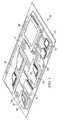
- FIG. 1illustrates a PCB with different types of packages mounted to its surface
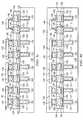
- FIGS. 2 a - 2 cillustrate further detail of the representative semiconductor packages mounted to the PCB
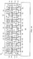
- FIGS. 3 a - 3 hillustrate a method of forming an interconnect structure with TSV for 3-D devices using an encapsulant for structural support
- FIGS. 4 a - 4 dillustrate a method of forming an interconnect structure with TSV and backside RDL for 3-D devices using an encapsulant for structural support.
- Front-end manufacturinginvolves the formation of a plurality of die on the surface of a semiconductor wafer.
- Each die on the wafercontains active and passive electrical components, which are electrically connected to form functional electrical circuits.
- Active electrical componentssuch as transistors and diodes, have the ability to control the flow of electrical current.
- Passive electrical componentssuch as capacitors, inductors, resistors, and transformers, create a relationship between voltage and current necessary to perform electrical circuit functions.
- Passive and active componentsare formed over the surface of the semiconductor wafer by a series of process steps including doping, deposition, photolithography, etching, and planarization.
- Dopingintroduces impurities into the semiconductor material by techniques such as ion implantation or thermal diffusion.
- the doping processmodifies the electrical conductivity of semiconductor material in active devices, transforming the semiconductor material into an insulator, conductor, or dynamically changing the semiconductor material conductivity in response to an electric field or base current.
- Transistorscontain regions of varying types and degrees of doping arranged as necessary to enable the transistor to promote or restrict the flow of electrical current upon the application of the electric field or base current.
- Active and passive componentsare formed by layers of materials with different electrical properties.
- the layerscan be formed by a variety of deposition techniques determined in part by the type of material being deposited. For example, thin film deposition may involve chemical vapor deposition (CVD), physical vapor deposition (PVD), electrolytic plating, and electroless plating processes.
- CVDchemical vapor deposition
- PVDphysical vapor deposition
- electrolytic platingelectroless plating processes.
- Each layeris generally patterned to form portions of active components, passive components, or electrical connections between components.
- the layerscan be patterned using photolithography, which involves the deposition of light sensitive material, e.g., photoresist, over the layer to be patterned.
- a patternis transferred from a photomask to the photoresist using light.
- the portion of the photoresist pattern subjected to lightis removed using a solvent, exposing portions of the underlying layer to be patterned.
- the remainder of the photoresistis removed, leaving behind a patterned layer.
- some types of materialsare patterned by directly depositing the material into the areas or voids formed by a previous deposition/etch process using techniques such as electroless and electrolytic plating.
- Planarizationcan be used to remove material from the surface of the wafer and produce a uniformly flat surface. Planarization involves polishing the surface of the wafer with a polishing pad. An abrasive material and corrosive chemical are added to the surface of the wafer during polishing. The combined mechanical action of the abrasive and corrosive action of the chemical removes any irregular topography, resulting in a uniformly flat surface.
- Back-end manufacturingrefers to cutting or singulating the finished wafer into the individual die and then packaging the die for structural support and environmental isolation.
- the waferis scored and broken along non-functional regions of the wafer called saw streets or scribes.
- the waferis singulated using a laser cutting tool or saw blade.
- the individual dieare mounted to a package substrate that includes pins or contact pads for interconnection with other system components.
- Contact pads formed over the semiconductor dieare then connected to contact pads within the package.
- the electrical connectionscan be made with solder bumps, stud bumps, conductive paste, or wirebonds.
- An encapsulant or other molding materialis deposited over the package to provide physical support and electrical isolation.
- the finished packageis then inserted into an electrical system and the functionality of the semiconductor device is made available to the other system components.
- FIG. 1illustrates electronic device 50 having a chip carrier substrate or PCB 52 with a plurality of semiconductor packages mounted on its surface.
- Electronic device 50may have one type of semiconductor package, or multiple types of semiconductor packages, depending on the application. The different types of semiconductor packages are shown in FIG. 1 for purposes of illustration.
- Electronic device 50may be a stand-alone system that uses the semiconductor packages to perform one or more electrical functions. Alternatively, electronic device 50 may be a subcomponent of a larger system. For example, electronic device 50 may be a graphics card, network interface card, or other signal processing card that can be inserted into a computer.
- the semiconductor packagecan include microprocessors, memories, application specific integrated circuits (ASICs), logic circuits, analog circuits, RF circuits, discrete devices, or other semiconductor die or electrical components.
- PCB 52provides a general substrate for structural support and electrical interconnect of the semiconductor packages mounted on the PCB.
- Conductive signal traces 54are formed over a surface or within layers of PCB 52 using evaporation, electrolytic plating, electroless plating, screen printing, or other suitable metal deposition process. Signal traces 54 provide for electrical communication between each of the semiconductor packages, mounted components, and other external system components. Traces 54 also provide power and ground connections to each of the semiconductor packages.
- a semiconductor devicehas two packaging levels.
- First level packagingis a technique for mechanically and electrically attaching the semiconductor die to an intermediate carrier.
- Second level packaginginvolves mechanically and electrically attaching the intermediate carrier to the PCB.
- a semiconductor devicemay only have the first level packaging where the die is mechanically and electrically mounted directly to the PCB.
- first level packagingincluding wire bond package 56 and flip chip 58
- second level packagingincluding ball grid array (BGA) 60 , bump chip carrier (BCC) 62 , dual in-line package (DIP) 64 , land grid array (LGA) 66 , multi-chip module (MCM) 68 , quad flat non-leaded package (QFN) 70 , and quad flat package 72 .
- BGAball grid array
- BCCbump chip carrier
- DIPdual in-line package
- LGAland grid array
- MCMmulti-chip module
- QFNquad flat non-leaded package
- quad flat package 72quad flat package
- electronic device 50includes a single attached semiconductor package, while other embodiments call for multiple interconnected packages.
- manufacturerscan incorporate pre-made components into electronic devices and systems. Because the semiconductor packages include sophisticated functionality, electronic devices can be manufactured using cheaper components and a streamlined manufacturing process. The resulting devices are less likely to fail and less expensive to manufacture resulting in a lower cost for consumers.
- FIGS. 2 a - 2 cshow exemplary semiconductor packages.
- FIG. 2 aillustrates further detail of DIP 64 mounted on PCB 52 .
- Semiconductor die 74includes an active region containing analog or digital circuits implemented as active devices, passive devices, conductive layers, and dielectric layers formed within the die and are electrically interconnected according to the electrical design of the die.
- the circuitmay include one or more transistors, diodes, inductors, capacitors, resistors, and other circuit elements formed within the active region of semiconductor die 74 .
- Contact pads 76are one or more layers of conductive material, such as aluminum (Al), copper (Cu), tin (Sn), nickel (Ni), gold (Au), or silver (Ag), and are electrically connected to the circuit elements formed within semiconductor die 74 .
- semiconductor die 74is mounted to an intermediate carrier 78 using a gold-silicon eutectic layer or adhesive material such as thermal epoxy.
- the package bodyincludes an insulative packaging material such as polymer or ceramic.
- Conductor leads 80 and wire bonds 82provide electrical interconnect between semiconductor die 74 and PCB 52 .
- Encapsulant 84is deposited over the package for environmental protection by preventing moisture and particles from entering the package and contaminating die 74 or wire bonds 82 .
- FIG. 2 billustrates further detail of BCC 62 mounted on PCB 52 .
- Semiconductor die 88is mounted over carrier 90 using an underfill or epoxy-resin adhesive material 92 .
- Wire bonds 94provide first level packing interconnect between contact pads 96 and 98 .
- Molding compound or encapsulant 100is deposited over semiconductor die 88 and wire bonds 94 to provide physical support and electrical isolation for the device.
- Contact pads 102are formed over a surface of PCB 52 using a suitable metal deposition such electrolytic plating or electroless plating to prevent oxidation.
- Contact pads 102are electrically connected to one or more conductive signal traces 54 in PCB 52 .
- Bumps 104are formed between contact pads 98 of BCC 62 and contact pads 102 of PCB 52 .
- semiconductor die 58is mounted face down to intermediate carrier 106 with a flip chip style first level packaging.
- Active region 108 of semiconductor die 58contains analog or digital circuits implemented as active devices, passive devices, conductive layers, and dielectric layers formed according to the electrical design of the die.
- the circuitmay include one or more transistors, diodes, inductors, capacitors, resistors, and other circuit elements within active region 108 .
- Semiconductor die 58is electrically and mechanically connected to carrier 106 through bumps 110 .
- BGA 60is electrically and mechanically connected to PCB 52 with a BGA style second level packaging using bumps 112 .
- Semiconductor die 58is electrically connected to conductive signal traces 54 in PCB 52 through bumps 110 , signal lines 114 , and bumps 112 .
- a molding compound or encapsulant 116is deposited over semiconductor die 58 and carrier 106 to provide physical support and electrical isolation for the device.
- the flip chip semiconductor deviceprovides a short electrical conduction path from the active devices on semiconductor die 58 to conduction tracks on PCB 52 in order to reduce signal propagation distance, lower capacitance, and improve overall circuit performance.
- the semiconductor die 58can be mechanically and electrically connected directly to PCB 52 using flip chip style first level packaging without intermediate carrier 106 .
- FIGS. 3 a - 3 hillustrate a process of forming an interconnect structure with a conductive via for 3-D devices using an encapsulant for structural support.
- a semiconductor wafer 118contains a substrate made with a base material such as silicon, polymer, polymer composite, metal, ceramic, glass, glass epoxy, beryllium oxide, or other suitable low-cost, rigid material for structural support.
- the substratecan be a semiconductor base material such as germanium, gallium arsenide, indium phosphide, or silicon carbide.
- a plurality of semiconductor diecan be formed on the substrate using semiconductor manufacturing processes such as described above.
- Each semiconductor dieincludes an active region 120 containing analog or digital circuits implemented as active devices, passive devices, conductive layers, and dielectric layers formed within the die and electrically interconnected according to the electrical design and function of the die.
- the circuitmay include one or more transistors, diodes, and other circuit elements formed within active surface 120 to implement baseband analog circuits or digital circuits, such as digital signal processor (DSP), ASIC, memory, or other signal processing circuit.
- DSPdigital signal processor
- the semiconductor diemay also contain integrated passive devices (IPD), such as inductors, capacitors, and resistors, for radio frequency (RF) signal processing.
- IPDintegrated passive devices
- the IPDs contained within semiconductor wafer 118provide the electrical characteristics needed for high frequency applications, such as resonators, high-pass filters, low-pass filters, band-pass filters, symmetric Hi-Q resonant transformers, matching networks, and tuning capacitors.
- the IPDscan be used as front-end wireless RF components, which can be positioned between the antenna and transceiver.
- the inductorcan be a hi-Q balun, transformer, or coil, operating up to 100 Gigahertz. In some applications, multiple baluns are formed on a same substrate, allowing multi-band operation.
- balunsare used in a quad-band for mobile phones or other global system for mobile (GSM) communications, each balun dedicated for a frequency band of operation of the quad-band device.
- GSMglobal system for mobile
- a typical RF systemrequires multiple IPDs and other high frequency circuits in one or more semiconductor packages to perform the necessary electrical functions.
- a plurality of viasis formed in semiconductor wafer 118 using laser drilling or etching process, such as deep reactive ion etching (DRIE).
- An insulating layer 121is formed to line the sidewalls and bottom of the vias.
- the insulating layer 121can be one or more layers of silicon dioxide (SiO2), silicon nitride (Si3N4), silicon oxynitride (SiON), tantalum pentoxide (Ta2O5), aluminum oxide (Al203), polyimide, benzocyclobutene (BCB), polybenzoxazoles (PBO), or other suitable dielectric material.
- the insulating layer 121is formed using PVD, CVD, or thermal oxidation.
- An electrically conductive material 122is deposited in the vias over insulating layer 121 using PVD, CVD, sputtering, electrolytic plating, electroless plating process, or other suitable metal deposition process.
- Conductive material 122can be one or more layers of Al, Cu, Sn, Ni, Au, Ag, W, poly-silicon, or other suitable electrically conductive material.
- Conductive material 122 in the viasfunctions as conductive TSV.
- an electrically conductive layer 124is formed over TSVs 122 and semiconductor wafer 118 using PVD, CVD, sputtering, electrolytic plating, electroless plating process, or other suitable metal deposition process.
- Conductive layer 124can be one or more layers of Al, Cu, Sn, Ni, Au, Ag, or other suitable electrically conductive material. The individual portions of conductive layer 124 can be electrically common or electrically isolated depending on the function of the semiconductor device.
- An insulating or passivation layer 126is formed on conductive layer 124 and active surface 120 of semiconductor wafer 118 .
- the insulating layer 126can be one or more layers of SiO2, Si3N4, SiON, Ta2O5, Al2O3, or other material having similar insulating properties.
- the insulating layer 126is formed using PVD, CVD, printing, spin coating, spray coating, sintering, or thermal oxidation. A portion of insulating layer 126 is removed by an etching process to expose conductive layer 124 .
- An electrically conductive layer 128is formed over conductive layer 124 and insulating layer 126 using PVD, CVD, sputtering, electrolytic plating, electroless plating process, or other suitable metal deposition process.
- Conductive layer 128can be one or more layers of Al, Cu, Sn, Ni, Au, Ag, or other suitable electrically conductive material. The individual portions of conductive layer 128 can be electrically common or electrically isolated depending on the function of the semiconductor device.
- An insulating or passivation layer 130is formed on conductive layer 128 and insulating layer 126 .
- the insulating layer 130can be one or more layers of SiO2, Si3N4, SiON, Ta2O5, Al2O3, or other material having similar insulating properties.
- the insulating layer 130is formed using PVD, CVD, printing, spin coating, spray coating, sintering, or thermal oxidation. A portion of insulating layer 130 is removed by plasma or chemical etching process to expose conductive layer 128 .
- Conductive pillars or posts 132are formed over conductive layer 128 .
- Conductive pillars 132can be Cu, Al, W, Au, solder, or other suitable electrically conductive material. In one embodiment, the conductive pillars 132 can be Cu and formed by a plating process.
- a thick layer of photoresistis deposited over insulating layer 130 and conductive layer 128 .
- the photoresistcan be a liquid or a dry film with a thickness of 15 to 130 ⁇ m. Two layers of photoresist may be applied to achieve the desired thickness.
- conductive pillarshave a height of 2-120 ⁇ m. The photoresist is patterned using photolithography.
- Cuis deposited in the patterned areas of the photoresist using electrolytic plating.
- the photoresistis stripped away leaving behind individual conductive pillars 132 .
- solder balls or stud bumpscan be formed over conductive layer 128 .
- An insulating or passivation layer 134is formed around conductive pillars 132 .
- the insulating layer 134can be one or more layers of SiO2, Si3N4, SiON, Ta2O5, Al2O3, or other material having similar insulating properties.
- the insulating layer 134is formed using PVD, CVD, printing, spin coating, spray coating, sintering, or thermal oxidation. A portion of insulating layer 134 is removed by an etching process to expose conductive pillar 132 .
- an electrically conductive layer 136is formed over conductive pillars 132 using PVD, CVD, sputtering, electrolytic plating, electroless plating process, or other suitable metal deposition process.
- Conductive layer 136can be one or more layers of Al, Cu, Sn, Ni, Au, Ag, or other suitable electrically conductive material.
- Conductive layer 136is an under bump metallization (UBM) in electrical contact with conductive pillar 132 .
- UBM 136can be a multi-metal stack with adhesion layer, barrier layer, and seed or wetting layer.
- the adhesion layeris formed over conductive pillar 132 and can be Ti, titanium nitride (TiN), titanium tungsten (TiW), Al, or chromium (Cr).
- the barrier layeris formed over the adhesion layer and can be made of Ni, nickel vanadium (NiV), platinum (Pt), palladium (Pd), TiW, or chromium copper (CrCu).
- the barrier layerinhibits the diffusion of Cu into the active area of the die.
- the seed layercan be Cu, Ni, NiV, Au, or Al.
- the seed layeris formed over the barrier layer and acts as an intermediate conductive layer between conductive pillar 132 and subsequent bumps or other interconnect structure.
- UBM 136provides a low resistive interconnect to conductive pillar 132 , as well as a barrier to solder diffusion and seed layer for solder wettability.
- An electrically conductive materialis deposited over UBM 136 using an evaporation, electrolytic plating, electroless plating, ball drop, or screen printing process.
- the conductive materialcan be Al, Sn, Ni, Au, Ag, Pb, Bi, Cu, solder, and combinations thereof, with an optional flux material.
- the conductive materialcan be eutectic Sn/Pb, high-lead solder, or lead-free solder.
- the conductive materialis bonded to UBM 136 using a suitable attachment or bonding process. In one embodiment, the conductive material is reflowed by heating the material above its melting point to form spherical balls or bumps 138 .
- bumps 138are reflowed a second time to improve electrical contact to UBM 136 .
- the bumpscan also be compression bonded to UBM 136 .
- Bumps 138represent one type of interconnect structure that can be formed over UBM 136 .
- the interconnect structurecan also use bond wires, conductive paste, stud bump, micro bump, or other electrical interconnect.
- Semiconductor die 140each have contact pads 142 metallurgically and electrically connected to bumps 138 .
- Each semiconductor die 140includes a substrate with an active region containing analog or digital circuits implemented as active devices, passive devices, conductive layers, and dielectric layers formed within the die and electrically interconnected according to the electrical design and function of the die.
- the semiconductor diemay also contain IPD for RF signal processing.
- a passive device or component 144is structurally and electrically connected to UBM 136 using bonds 146 .
- Semiconductor die 140 and passive device 144in combination with the IPD formed in active region 120 , provide a 3-D semiconductor structure.
- FIG. 3 dshows an encapsulant or molding compound 150 deposited over the structure described in FIG. 3 c using a paste printing, compressive molding, transfer molding, liquid encapsulant molding, or other suitable applicator.
- Encapsulant 150can be epoxy resin, epoxy acrylate, polymer, or polymer composite material.
- Encapsulant 150is non-conductive and environmentally protects the semiconductor device from external elements and contaminants.
- semiconductor wafer 118is inverted and back surface 152 is reduced in thickness by mechanical grinding, CMP, wet etching, dry etching, plasma etching, or another thinning process. Since semiconductor wafer 118 is covered with encapsulant 150 , the structure is sufficiently robust to reduce substrate thickness to less than 300 ⁇ m. In one embodiment, the thickness of the substrate is reduced to 10-50 ⁇ m. A temporary carrier or tape is not needed because encapsulant 150 provides the support to maintain the structural integrity of the device, even with the reduced substrate thickness.
- an insulating or passivation layer 154is formed over back surface 152 and TSVs 122 .
- the insulating layer 154can be one or more layers of SiO2, Si3N4, SiON, Ta2O5, Al2O3, or other material having similar insulating properties.
- the insulating layer 154is formed using PVD, CVD, printing, spin coating, spray coating, sintering, or thermal oxidation. A portion of insulating layer 154 is removed by an etching process to expose TSVs 122 .
- An electrically conductive layer 156is formed over TSVs 122 and insulating layer 154 using PVD, CVD, sputtering, electrolytic plating, electroless plating process, or other suitable metal deposition process.
- Conductive layer 156can be one or more layers of Al, Cu, Sn, Ni, Au, Ag, or other suitable electrically conductive material.
- Conductive layer 156is a UBM in electrical contact with TSVs 122 .
- an electrically conductive materialis deposited over UBM 156 using an evaporation, electrolytic plating, electroless plating, ball drop, or screen printing process.
- the conductive materialcan be Al, Sn, Ni, Au, Ag, Pb, Bi, Cu, solder, and combinations thereof, with an optional flux material.
- the conductive materialcan be eutectic Sn/Pb, high-lead solder, or lead-free solder.
- the conductive materialis bonded to UBM 156 using a suitable attachment or bonding process. In one embodiment, the conductive material is reflowed by heating the material above its melting point to form spherical balls or bumps 158 .
- bumps 158are reflowed a second time to improve electrical contact to UBM 156 .
- the bumpscan also be compression bonded to UBM 156 .
- Bumps 158represent one type of interconnect structure that can be formed over UBM 156 .
- the interconnect structurecan also use bond wires, conductive paste, stud bump, micro bump, or other electrical interconnect.
- semiconductor wafer 118is inverted again and singulated into semiconductor devices 160 , which are metallurgically and electrically connected to contact pads 166 on PCB 168 using bumps 158 .
- Semiconductor die 140 and passive device 144as well as passive and active devices in active region 120 , electrically connect to PCB 168 through bumps 138 and 158 , UBMs 136 and 156 , TSV 122 , conductive pillars 132 , bonds 146 , and conductive layers 124 and 128 .
- the encapsulation processmakes the substrate or wafer structurally robust during formation of additional interconnect structures.
- the encapsulantpermits backside grinding to substantially reduce its thickness.
- the electrical connection to PCB 168is made on the backside of the wafer with TSVs 122 thus reducing the silicon area and package size and increasing device performance.
- the encapsulanteliminates the need for bonding & de-bonding to a temporary carrier, lowers manufacturing cost, reduces breakage and slip, simplifies handling, and enables higher processing temperatures.
- the electrical connection to the PCB on the backside of the substratereduces silicon area and corresponding package size and thickness.
- FIGS. 3 a - 3 dAnother embodiment of forming an interconnect structure for 3-D devices using the process flow of FIGS. 3 a - 3 d .
- TSVs 122 , conductive layers 124 and 128 , UBM 136 , conductive pillars 132 , bumps 138 , semiconductor die 140 , passive device 144 , bonds 146 , and insulating layers 126 , 130 , and 134have been formed on semiconductor wafer 118 .
- Encapsulant 150is deposited over the structure 122 - 146 for structural support during formation of additional interconnect structures.
- semiconductor wafer 118is inverted and back surface 152 is reduced in thickness by mechanical grinding, CMP, wet etching, dry etching, plasma etching, or another thinning process. Since semiconductor wafer 118 is covered with encapsulant 150 , the structure is sufficiently robust to reduce substrate thickness to less than 300 ⁇ m. In one embodiment, the thickness of the substrate is reduced to 10-50 ⁇ m. A temporary carrier or tape is not needed because encapsulant 150 provides the support to maintain the structural integrity of the device, even with the reduced substrate thickness.
- An insulating or passivation layer 170is formed over back surface 152 and TSVs 122 .
- the insulating layer 170can be one or more layers of SiO2, Si3N4, SiON, Ta2O5, Al2O3, or other material having similar insulating properties.
- the insulating layer 170is formed using PVD, CVD, printing, spin coating, spray coating, sintering, or thermal oxidation. A portion of insulating layer 170 is removed by an etching process to expose TSVs 122 .
- An electrically conductive layer 172is formed over TSVs 122 and insulating layer 170 using PVD, CVD, sputtering, electrolytic plating, electroless plating process, or other suitable metal deposition process.
- Conductive layer 172can be one or more layers of Al, Cu, Sn, Ni, Au, Ag, or other suitable electrically conductive material.
- Conductive layer 172is a redistribution layer (RDL) in electrical contact with TSVs 122 .
- RDL 172extends electrical connectivity of TSVs 122 .
- an insulating or passivation layer 174is formed over insulating layer 170 and RDLs 172 .
- the insulating layer 174can be one or more layers of SiO2, Si3N4, SiON, Ta2O5, Al2O3, or other material having similar insulating properties.
- the insulating layer 174is formed using PVD, CVD, printing, spin coating, spray coating, sintering, or thermal oxidation. A portion of insulating layer 174 is removed by an etching process to expose RDLs 172 .
- An electrically conductive layer 176is formed over RDLs 172 and insulating layer 174 using PVD, CVD, sputtering, electrolytic plating, electroless plating process, or other suitable metal deposition process.
- Conductive layer 176can be one or more layers of Al, Cu, Sn, Ni, Au, Ag, or other suitable electrically conductive material.
- Conductive layer 176is a UBM in electrical contact with RDLs 172 .
- an electrically conductive materialis deposited over UBM 176 using an evaporation, electrolytic plating, electroless plating, ball drop, or screen printing process.
- the conductive materialcan be Al, Sn, Ni, Au, Ag, Pb, Bi, Cu, solder, and combinations thereof, with an optional flux material.
- the conductive materialcan be eutectic Sn/Pb, high-lead solder, or lead-free solder.
- the conductive materialis bonded to UBM 176 using a suitable attachment or bonding process. In one embodiment, the conductive material is reflowed by heating the material above its melting point to form spherical balls or bumps 178 .
- bumps 178are reflowed a second time to improve electrical contact to UBM 176 .
- the bumpscan also be compression bonded to UBM 176 .
- Bumps 178represent one type of interconnect structure that can be formed over UBM 176 .
- the interconnect structurecan also use bond wires, conductive paste, stud bump, micro bump, or other electrical interconnect.
- semiconductor wafer 118is inverted again and singulated into semiconductor devices 180 , which are metallurgically and electrically connected to contact pads 186 on PCB 188 using bumps 178 .
- Semiconductor die 140 and passive device 144as well as passive and active devices in active region 120 , electrically connect to PCB 188 through bumps 138 and 158 , RDL 172 , TSV 122 , UBMs 136 and 156 , conductive pillars 132 , bonds 146 , and conductive layers 124 and 128 .
- the encapsulation processmakes the substrate or wafer structurally robust during formation of additional interconnect structures.
- the encapsulantpermits backside grinding to substantially reduce its thickness.
- the electrical connection to PCB 188is made on the backside of the wafer with TSVs 122 thus reducing the silicon area and package size and increasing device performance.
- the encapsulanteliminates the need for bonding & de-bonding to a temporary carrier, lowers manufacturing cost, reduces breakage and slip, simplifies handling, and enables higher processing temperatures.
- the electrical connection to the PCB on the backside of the substratereduces silicon area and corresponding package size and thickness.
Landscapes
- Engineering & Computer Science (AREA)
- Microelectronics & Electronic Packaging (AREA)
- Computer Hardware Design (AREA)
- Power Engineering (AREA)
- Physics & Mathematics (AREA)
- Condensed Matter Physics & Semiconductors (AREA)
- General Physics & Mathematics (AREA)
- Manufacturing & Machinery (AREA)
- Ceramic Engineering (AREA)
- Internal Circuitry In Semiconductor Integrated Circuit Devices (AREA)
- Structures Or Materials For Encapsulating Or Coating Semiconductor Devices Or Solid State Devices (AREA)
Abstract
Description
Claims (27)
Priority Applications (5)
| Application Number | Priority Date | Filing Date | Title |
|---|---|---|---|
| US12/480,317US8067308B2 (en) | 2009-06-08 | 2009-06-08 | Semiconductor device and method of forming an interconnect structure with TSV using encapsulant for structural support |
| SG2012050738ASG183014A1 (en) | 2009-06-08 | 2010-04-13 | Semiconductor device having an interconnect structure with tsv using encapsulant for structural support |
| TW099114343ATWI567866B (en) | 2009-06-08 | 2010-05-05 | Semiconductor device and method of forming an interconnect structure with tsv using encapsulant for structural support |
| US13/245,099US8659162B2 (en) | 2009-06-08 | 2011-09-26 | Semiconductor device having an interconnect structure with TSV using encapsulant for structural support |
| US14/143,891US9054083B2 (en) | 2009-06-08 | 2013-12-30 | Semiconductor device and method of making TSV interconnect structures using encapsulant for structural support |
Applications Claiming Priority (1)
| Application Number | Priority Date | Filing Date | Title |
|---|---|---|---|
| US12/480,317US8067308B2 (en) | 2009-06-08 | 2009-06-08 | Semiconductor device and method of forming an interconnect structure with TSV using encapsulant for structural support |
Related Child Applications (1)
| Application Number | Title | Priority Date | Filing Date |
|---|---|---|---|
| US13/245,099DivisionUS8659162B2 (en) | 2009-06-08 | 2011-09-26 | Semiconductor device having an interconnect structure with TSV using encapsulant for structural support |
Publications (2)
| Publication Number | Publication Date |
|---|---|
| US20100308443A1 US20100308443A1 (en) | 2010-12-09 |
| US8067308B2true US8067308B2 (en) | 2011-11-29 |
Family
ID=43300147
Family Applications (3)
| Application Number | Title | Priority Date | Filing Date |
|---|---|---|---|
| US12/480,317ActiveUS8067308B2 (en) | 2009-06-08 | 2009-06-08 | Semiconductor device and method of forming an interconnect structure with TSV using encapsulant for structural support |
| US13/245,099Active2029-11-22US8659162B2 (en) | 2009-06-08 | 2011-09-26 | Semiconductor device having an interconnect structure with TSV using encapsulant for structural support |
| US14/143,891ActiveUS9054083B2 (en) | 2009-06-08 | 2013-12-30 | Semiconductor device and method of making TSV interconnect structures using encapsulant for structural support |
Family Applications After (2)
| Application Number | Title | Priority Date | Filing Date |
|---|---|---|---|
| US13/245,099Active2029-11-22US8659162B2 (en) | 2009-06-08 | 2011-09-26 | Semiconductor device having an interconnect structure with TSV using encapsulant for structural support |
| US14/143,891ActiveUS9054083B2 (en) | 2009-06-08 | 2013-12-30 | Semiconductor device and method of making TSV interconnect structures using encapsulant for structural support |
Country Status (3)
| Country | Link |
|---|---|
| US (3) | US8067308B2 (en) |
| SG (1) | SG183014A1 (en) |
| TW (1) | TWI567866B (en) |
Cited By (12)
| Publication number | Priority date | Publication date | Assignee | Title |
|---|---|---|---|---|
| US20110195545A1 (en)* | 2010-02-11 | 2011-08-11 | Advanced Semiconductor Engineering, Inc. | Package process |
| US20120013004A1 (en)* | 2009-06-08 | 2012-01-19 | Stats Chippac, Ltd. | Semiconductor Device Having an Interconnect Structure with TSV Using Encapsulant for Structural Support |
| US20120187578A1 (en)* | 2009-08-06 | 2012-07-26 | Ming Li | Packaged semiconductor device for high performance memory and logic |
| US20120190173A1 (en)* | 2011-01-20 | 2012-07-26 | Jia-Jin Tu | Method for packaging wafer |
| US20140070424A1 (en)* | 2012-09-10 | 2014-03-13 | Siliconware Precision Industries Co., Ltd. | Semiconductor package, method of fabricating the semiconductor package, and interposer structure of the semiconductor package |
| US20150262846A1 (en)* | 2014-03-13 | 2015-09-17 | Taiwan Semiconductor Manufacturing Co., Ltd | Package structure and manufacturing method |
| US9508671B2 (en) | 2015-04-20 | 2016-11-29 | Advanced Semiconductor Engineering, Inc. | Semiconductor device and semiconductor package |
| US9831148B2 (en)* | 2016-03-11 | 2017-11-28 | Taiwan Semiconductor Manufacturing Company, Ltd. | Integrated fan-out package including voltage regulators and methods forming same |
| US10163851B2 (en) | 2015-11-30 | 2018-12-25 | Taiwan Semiconductor Manufacturing Company, Ltd. | Tri-layer CoWoS structure |
| US10553487B2 (en) | 2014-06-26 | 2020-02-04 | STATS ChipPAC Pte. Ltd. | Semiconductor device and method of forming conductive vias by direct via reveal with organic passivation |
| US20220272842A1 (en)* | 2020-12-15 | 2022-08-25 | Tdk Corporation | Electric circuit module and manufacturing method thereof |
| US12369258B2 (en) | 2020-12-15 | 2025-07-22 | Tdk Corporation | Electronic circuit module |
Families Citing this family (61)
| Publication number | Priority date | Publication date | Assignee | Title |
|---|---|---|---|---|
| TWI579995B (en)* | 2009-08-19 | 2017-04-21 | Xintex Inc | Chip package and method of manufacturing same |
| US8242604B2 (en)* | 2009-10-28 | 2012-08-14 | International Business Machines Corporation | Coaxial through-silicon via |
| US8476775B2 (en)* | 2009-12-17 | 2013-07-02 | Stats Chippac Ltd. | Integrated circuit packaging system with embedded interconnect and method of manufacture thereof |
| KR101095373B1 (en)* | 2010-04-22 | 2011-12-16 | 재단법인 서울테크노파크 | Semiconductor chip comprising bump having barrier layer and method for manufacturing same |
| US9048233B2 (en) | 2010-05-26 | 2015-06-02 | Taiwan Semiconductor Manufacturing Company, Ltd. | Package systems having interposers |
| US8426961B2 (en)* | 2010-06-25 | 2013-04-23 | Taiwan Semiconductor Manufacturing Company, Ltd. | Embedded 3D interposer structure |
| US8232193B2 (en) | 2010-07-08 | 2012-07-31 | Taiwan Semiconductor Manufacturing Company, Ltd. | Method of forming Cu pillar capped by barrier layer |
| US9224647B2 (en) | 2010-09-24 | 2015-12-29 | Stats Chippac, Ltd. | Semiconductor device and method of forming TSV interposer with semiconductor die and build-up interconnect structure on opposing surfaces of the interposer |
| US8993377B2 (en) | 2010-09-29 | 2015-03-31 | Stats Chippac, Ltd. | Semiconductor device and method of bonding different size semiconductor die at the wafer level |
| US9704766B2 (en)* | 2011-04-28 | 2017-07-11 | Taiwan Semiconductor Manufacturing Company, Ltd. | Interposers of 3-dimensional integrated circuit package systems and methods of designing the same |
| US8803269B2 (en) | 2011-05-05 | 2014-08-12 | Cisco Technology, Inc. | Wafer scale packaging platform for transceivers |
| US20120286416A1 (en)* | 2011-05-11 | 2012-11-15 | Tessera Research Llc | Semiconductor chip package assembly and method for making same |
| US8409927B1 (en)* | 2011-09-23 | 2013-04-02 | GlobalFoundries, Inc. | Methods for fabricating integrated circuit systems including high reliability die under-fill |
| US8872312B2 (en)* | 2011-09-30 | 2014-10-28 | Taiwan Semiconductor Manufacturing Company, Ltd. | EMI package and method for making same |
| KR101932665B1 (en)* | 2011-10-10 | 2018-12-27 | 삼성전자 주식회사 | Semiconductor package |
| CN103050436B (en)* | 2011-10-17 | 2017-10-10 | 新科金朋有限公司 | Form the semiconductor devices and method of the conductive pole with extension substrate |
| US9824923B2 (en)* | 2011-10-17 | 2017-11-21 | STATS ChipPAC Pte. Ltd. | Semiconductor device and method of forming conductive pillar having an expanded base |
| US20130113084A1 (en)* | 2011-11-04 | 2013-05-09 | Roden R. Topacio | Semiconductor substrate with molded support layer |
| US9646942B2 (en)* | 2012-02-23 | 2017-05-09 | Taiwan Semiconductor Manufacturing Company, Ltd. | Mechanisms for controlling bump height variation |
| US10049964B2 (en) | 2012-03-23 | 2018-08-14 | STATS ChipPAC Pte. Ltd. | Semiconductor device and method of forming a fan-out PoP device with PWB vertical interconnect units |
| US9837303B2 (en) | 2012-03-23 | 2017-12-05 | STATS ChipPAC Pte. Ltd. | Semiconductor method and device of forming a fan-out device with PWB vertical interconnect units |
| US9842798B2 (en) | 2012-03-23 | 2017-12-12 | STATS ChipPAC Pte. Ltd. | Semiconductor device and method of forming a PoP device with embedded vertical interconnect units |
| US8810024B2 (en) | 2012-03-23 | 2014-08-19 | Stats Chippac Ltd. | Semiconductor method and device of forming a fan-out PoP device with PWB vertical interconnect units |
| US20130249095A1 (en)* | 2012-03-26 | 2013-09-26 | Skyworks Solutions, Inc. | Gallium arsenide devices with copper backside for direct die solder attach |
| EP2648214B1 (en) | 2012-04-05 | 2019-06-12 | ams AG | Methods of producing a semiconductor device with a through-substrate via |
| CN103378057B (en)* | 2012-04-20 | 2016-06-29 | 南亚科技股份有限公司 | Semiconductor chip and method of forming same |
| CN103378059B (en)* | 2012-04-27 | 2016-04-27 | 南亚科技股份有限公司 | Through-silicon vias and methods of forming them |
| US9040346B2 (en) | 2012-05-03 | 2015-05-26 | Infineon Technologies Ag | Semiconductor package and methods of formation thereof |
| TWI467733B (en)* | 2012-05-16 | 2015-01-01 | 矽品精密工業股份有限公司 | Semiconductor package and method of forming same |
| US20130313710A1 (en)* | 2012-05-22 | 2013-11-28 | Micron Technology, Inc. | Semiconductor Constructions and Methods of Forming Semiconductor Constructions |
| TWI484610B (en) | 2012-07-09 | 2015-05-11 | 矽品精密工業股份有限公司 | Method of forming semiconductor structure and conductive bump |
| TWI544599B (en)* | 2012-10-30 | 2016-08-01 | 矽品精密工業股份有限公司 | Fabrication method of package structure |
| US9799592B2 (en)* | 2013-11-19 | 2017-10-24 | Amkor Technology, Inc. | Semicondutor device with through-silicon via-less deep wells |
| US9123789B2 (en)* | 2013-01-23 | 2015-09-01 | United Microelectronics Corp. | Chip with through silicon via electrode and method of forming the same |
| US9351436B2 (en)* | 2013-03-08 | 2016-05-24 | Cochlear Limited | Stud bump bonding in implantable medical devices |
| US9130022B2 (en)* | 2013-03-15 | 2015-09-08 | Taiwan Semiconductor Manufacturing Co., Ltd. | Method of back-end-of-line (BEOL) fabrication, and devices formed by the method |
| US9685414B2 (en)* | 2013-06-26 | 2017-06-20 | Intel Corporation | Package assembly for embedded die and associated techniques and configurations |
| US20150041183A1 (en)* | 2013-08-06 | 2015-02-12 | Kinsus Interconnect Technology Corp. | Chip board package structure |
| US9076724B1 (en)* | 2013-09-26 | 2015-07-07 | Stats Chippac Ltd. | Integrated circuit system with debonding adhesive and method of manufacture thereof |
| US9524942B2 (en)* | 2013-12-18 | 2016-12-20 | Taiwan Semiconductor Manufacturing Company, Ltd. | Chip-on-substrate packaging on carrier |
| US9553059B2 (en)* | 2013-12-20 | 2017-01-24 | Taiwan Semiconductor Manufacturing Company, Ltd. | Backside redistribution layer (RDL) structure |
| CN105271104B (en)* | 2014-06-06 | 2018-09-14 | 日月光半导体制造股份有限公司 | Method for manufacturing semiconductor packaging structure |
| US10115701B2 (en) | 2014-06-26 | 2018-10-30 | STATS ChipPAC Pte. Ltd. | Semiconductor device and method of forming conductive vias by backside via reveal with CMP |
| US9754928B2 (en)* | 2014-07-17 | 2017-09-05 | Taiwan Semiconductor Manufacturing Company, Ltd. | SMD, IPD, and/or wire mount in a package |
| US9613910B2 (en) | 2014-07-17 | 2017-04-04 | Taiwan Semiconductor Manufacturing Company, Ltd. | Anti-fuse on and/or in package |
| CN105731358B (en)* | 2014-12-08 | 2018-08-17 | 中芯国际集成电路制造(上海)有限公司 | A kind of MEMS device and preparation method thereof, electronic device |
| US9443799B2 (en)* | 2014-12-16 | 2016-09-13 | International Business Machines Corporation | Interposer with lattice construction and embedded conductive metal structures |
| US9786623B2 (en) | 2015-03-17 | 2017-10-10 | STATS ChipPAC Pte. Ltd. | Semiconductor device and method of forming PoP semiconductor device with RDL over top package |
| US20170098589A1 (en)* | 2015-10-05 | 2017-04-06 | Mediatek Inc. | Fan-out wafer level package structure |
| US20170148955A1 (en)* | 2015-11-22 | 2017-05-25 | Cyntec Co., Ltd. | Method of wafer level packaging of a module |
| CN109075151B (en) | 2016-04-26 | 2023-06-27 | 亚德诺半导体国际无限责任公司 | Lead frame for mechanical mating, and electrical and thermal conduction of component package circuits |
| US9842829B2 (en)* | 2016-04-29 | 2017-12-12 | Taiwan Semiconductor Manufacturing Co., Ltd. | Chip package structure and method for forming the same |
| US20180090471A1 (en)* | 2016-09-28 | 2018-03-29 | Intel Corporation | Package on Package Structure Having Package To Package Interconnect Composed of Packed Wires Having A Polygon Cross Section |
| CN109390373B (en)* | 2017-08-08 | 2020-09-29 | 上海视欧光电科技有限公司 | Packaging structure and packaging method thereof |
| TWI643307B (en)* | 2018-01-30 | 2018-12-01 | 矽品精密工業股份有限公司 | Electronic package and method for fabricating the same |
| US10497635B2 (en) | 2018-03-27 | 2019-12-03 | Linear Technology Holding Llc | Stacked circuit package with molded base having laser drilled openings for upper package |
| KR102530754B1 (en)* | 2018-08-24 | 2023-05-10 | 삼성전자주식회사 | Method for manufacturing semiconductor package having redistribution layer |
| JP7154913B2 (en) | 2018-09-25 | 2022-10-18 | 株式会社東芝 | Semiconductor device and its manufacturing method |
| US11410977B2 (en) | 2018-11-13 | 2022-08-09 | Analog Devices International Unlimited Company | Electronic module for high power applications |
| US11300727B2 (en)* | 2019-07-31 | 2022-04-12 | Advanced Semiconductor Engineering, Inc. | Optical communication package structure and method for manufacturing the same |
| US11844178B2 (en) | 2020-06-02 | 2023-12-12 | Analog Devices International Unlimited Company | Electronic component |
Citations (4)
| Publication number | Priority date | Publication date | Assignee | Title |
|---|---|---|---|---|
| US6002169A (en)* | 1998-06-15 | 1999-12-14 | Lsi Logic Corporation | Thermally enhanced tape ball grid array package |
| US20100140736A1 (en)* | 2008-12-10 | 2010-06-10 | Stats Chippac, Ltd. | Semiconductor Device and Method of Embedding Integrated Passive Devices into the Package Electrically Interconnected Using Conductive Pillars |
| US20100140751A1 (en)* | 2008-12-10 | 2010-06-10 | Stats Chippac, Ltd. | Semiconductor Device and Method of Forming a Conductive Via-in-Via Structure |
| US20100140815A1 (en)* | 2008-12-10 | 2010-06-10 | Stats Chippac, Ltd. | Semiconductor device and method of forming an interconnect structure for 3-d devices using encapsulant for structural support |
Family Cites Families (6)
| Publication number | Priority date | Publication date | Assignee | Title |
|---|---|---|---|---|
| US7060601B2 (en)* | 2003-12-17 | 2006-06-13 | Tru-Si Technologies, Inc. | Packaging substrates for integrated circuits and soldering methods |
| US7553752B2 (en)* | 2007-06-20 | 2009-06-30 | Stats Chippac, Ltd. | Method of making a wafer level integration package |
| US8722457B2 (en) | 2007-12-27 | 2014-05-13 | Stats Chippac, Ltd. | System and apparatus for wafer level integration of components |
| US7880293B2 (en) | 2008-03-25 | 2011-02-01 | Stats Chippac, Ltd. | Wafer integrated with permanent carrier and method therefor |
| US7993941B2 (en)* | 2008-12-05 | 2011-08-09 | Stats Chippac, Ltd. | Semiconductor package and method of forming Z-direction conductive posts embedded in structurally protective encapsulant |
| US8067308B2 (en)* | 2009-06-08 | 2011-11-29 | Stats Chippac, Ltd. | Semiconductor device and method of forming an interconnect structure with TSV using encapsulant for structural support |
- 2009
- 2009-06-08USUS12/480,317patent/US8067308B2/enactiveActive
- 2010
- 2010-04-13SGSG2012050738Apatent/SG183014A1/enunknown
- 2010-05-05TWTW099114343Apatent/TWI567866B/enactive
- 2011
- 2011-09-26USUS13/245,099patent/US8659162B2/enactiveActive
- 2013
- 2013-12-30USUS14/143,891patent/US9054083B2/enactiveActive
Patent Citations (5)
| Publication number | Priority date | Publication date | Assignee | Title |
|---|---|---|---|---|
| US6002169A (en)* | 1998-06-15 | 1999-12-14 | Lsi Logic Corporation | Thermally enhanced tape ball grid array package |
| US20100140736A1 (en)* | 2008-12-10 | 2010-06-10 | Stats Chippac, Ltd. | Semiconductor Device and Method of Embedding Integrated Passive Devices into the Package Electrically Interconnected Using Conductive Pillars |
| US20100140751A1 (en)* | 2008-12-10 | 2010-06-10 | Stats Chippac, Ltd. | Semiconductor Device and Method of Forming a Conductive Via-in-Via Structure |
| US20100140815A1 (en)* | 2008-12-10 | 2010-06-10 | Stats Chippac, Ltd. | Semiconductor device and method of forming an interconnect structure for 3-d devices using encapsulant for structural support |
| US7741148B1 (en)* | 2008-12-10 | 2010-06-22 | Stats Chippac, Ltd. | Semiconductor device and method of forming an interconnect structure for 3-D devices using encapsulant for structural support |
Cited By (28)
| Publication number | Priority date | Publication date | Assignee | Title |
|---|---|---|---|---|
| US20120013004A1 (en)* | 2009-06-08 | 2012-01-19 | Stats Chippac, Ltd. | Semiconductor Device Having an Interconnect Structure with TSV Using Encapsulant for Structural Support |
| US8659162B2 (en)* | 2009-06-08 | 2014-02-25 | Stats Chippac, Ltd. | Semiconductor device having an interconnect structure with TSV using encapsulant for structural support |
| US20140110861A1 (en)* | 2009-06-08 | 2014-04-24 | Stats Chippac, Ltd. | Semiconductor Device Having an Interconnect Structure with TSV Using Encapsulant for Structural Support |
| US9054083B2 (en)* | 2009-06-08 | 2015-06-09 | Stats Chippac, Ltd. | Semiconductor device and method of making TSV interconnect structures using encapsulant for structural support |
| US9466561B2 (en)* | 2009-08-06 | 2016-10-11 | Rambus Inc. | Packaged semiconductor device for high performance memory and logic |
| US20120187578A1 (en)* | 2009-08-06 | 2012-07-26 | Ming Li | Packaged semiconductor device for high performance memory and logic |
| US8338235B2 (en)* | 2010-02-11 | 2012-12-25 | Advanced Semiconductor Engineering, Inc. | Package process of stacked type semiconductor device package structure |
| US20110195545A1 (en)* | 2010-02-11 | 2011-08-11 | Advanced Semiconductor Engineering, Inc. | Package process |
| US20120190173A1 (en)* | 2011-01-20 | 2012-07-26 | Jia-Jin Tu | Method for packaging wafer |
| US9548220B2 (en) | 2012-09-10 | 2017-01-17 | Siliconware Precision Industries Co., Ltd. | Method of fabricating semiconductor package having an interposer structure |
| TWI503928B (en)* | 2012-09-10 | 2015-10-11 | 矽品精密工業股份有限公司 | Method of manufacturing semiconductor package, semiconductor package and its interposers |
| US9257381B2 (en)* | 2012-09-10 | 2016-02-09 | Siliconware Precision Industries Co., Ltd. | Semiconductor package, and interposer structure of the semiconductor package |
| US20140070424A1 (en)* | 2012-09-10 | 2014-03-13 | Siliconware Precision Industries Co., Ltd. | Semiconductor package, method of fabricating the semiconductor package, and interposer structure of the semiconductor package |
| US20150262846A1 (en)* | 2014-03-13 | 2015-09-17 | Taiwan Semiconductor Manufacturing Co., Ltd | Package structure and manufacturing method |
| US9779969B2 (en)* | 2014-03-13 | 2017-10-03 | Taiwan Semiconductor Manufacturing Co., Ltd. | Package structure and manufacturing method |
| US10553487B2 (en) | 2014-06-26 | 2020-02-04 | STATS ChipPAC Pte. Ltd. | Semiconductor device and method of forming conductive vias by direct via reveal with organic passivation |
| US9508671B2 (en) | 2015-04-20 | 2016-11-29 | Advanced Semiconductor Engineering, Inc. | Semiconductor device and semiconductor package |
| US9768139B2 (en) | 2015-04-20 | 2017-09-19 | Advanced Semiconductor Engineering, Inc. | Semiconductor device and semiconductor package |
| US10163851B2 (en) | 2015-11-30 | 2018-12-25 | Taiwan Semiconductor Manufacturing Company, Ltd. | Tri-layer CoWoS structure |
| US10748870B2 (en) | 2015-11-30 | 2020-08-18 | Taiwan Semiconductor Manufacturing Company, Ltd. | Tri-layer COWOS structure |
| US11244924B2 (en) | 2015-11-30 | 2022-02-08 | Taiwan Semiconductor Manufacturing Company, Ltd. | Tri-layer CoWoS structure |
| US10163852B2 (en) | 2016-03-11 | 2018-12-25 | Taiwan Semiconductor Manufacturing Company, Ltd. | Integrated fan-out package including voltage regulators and methods forming same |
| US10497668B2 (en) | 2016-03-11 | 2019-12-03 | Taiwan Semiconductor Manufacturing Company, Ltd. | Integrated fan-out package including voltage regulators and methods forming same |
| US9831148B2 (en)* | 2016-03-11 | 2017-11-28 | Taiwan Semiconductor Manufacturing Company, Ltd. | Integrated fan-out package including voltage regulators and methods forming same |
| US11063016B2 (en) | 2016-03-11 | 2021-07-13 | Taiwan Semiconductor Manufacturing Company, Ltd. | Integrated fan-out package including voltage regulators and methods forming same |
| US20220272842A1 (en)* | 2020-12-15 | 2022-08-25 | Tdk Corporation | Electric circuit module and manufacturing method thereof |
| US11979988B2 (en)* | 2020-12-15 | 2024-05-07 | Tdk Corporation | Electric circuit module and manufacturing method thereof |
| US12369258B2 (en) | 2020-12-15 | 2025-07-22 | Tdk Corporation | Electronic circuit module |
Also Published As
| Publication number | Publication date |
|---|---|
| TW201101428A (en) | 2011-01-01 |
| US9054083B2 (en) | 2015-06-09 |
| SG183014A1 (en) | 2012-08-30 |
| US20120013004A1 (en) | 2012-01-19 |
| TWI567866B (en) | 2017-01-21 |
| US20140110861A1 (en) | 2014-04-24 |
| US20100308443A1 (en) | 2010-12-09 |
| US8659162B2 (en) | 2014-02-25 |
Similar Documents
| Publication | Publication Date | Title |
|---|---|---|
| US9054083B2 (en) | Semiconductor device and method of making TSV interconnect structures using encapsulant for structural support | |
| US7741148B1 (en) | Semiconductor device and method of forming an interconnect structure for 3-D devices using encapsulant for structural support | |
| US10083916B2 (en) | Semiconductor device and method of forming stress relief layer between die and interconnect structure | |
| US9263361B2 (en) | Semiconductor device having a vertical interconnect structure using stud bumps | |
| US8072059B2 (en) | Semiconductor device and method of forming UBM fixed relative to interconnect structure for alignment of semiconductor die | |
| US8790962B2 (en) | Semiconductor device and method of forming a shielding layer over a semiconductor die after forming a build-up interconnect structure | |
| US9343396B2 (en) | Semiconductor device and method of forming IPD in fan-out wafer level chip scale package | |
| US9524955B2 (en) | Semiconductor device and method of forming no-flow underfill material around vertical interconnect structure | |
| US8445990B2 (en) | Semiconductor device and method of forming an inductor within interconnect layer vertically separated from semiconductor die | |
| US11127666B2 (en) | Semiconductor device and method of forming openings through insulating layer over encapsulant for enhanced adhesion of interconnect structure | |
| SG185340A1 (en) | Semiconductor device and method of formingvertical interconnect structure using stud bumps |
Legal Events
| Date | Code | Title | Description |
|---|---|---|---|
| AS | Assignment | Owner name:STATS CHIPPAC, LTD., SINGAPORE Free format text:ASSIGNMENT OF ASSIGNORS INTEREST;ASSIGNORS:SUTHIWONGSUNTHORN, NATHAPONG;MARIMUTHU, PANDI C.;KU, JAE HUN;AND OTHERS;SIGNING DATES FROM 20090525 TO 20090527;REEL/FRAME:022794/0983 | |
| STCF | Information on status: patent grant | Free format text:PATENTED CASE | |
| FPAY | Fee payment | Year of fee payment:4 | |
| AS | Assignment | Owner name:CITICORP INTERNATIONAL LIMITED, AS COMMON SECURITY AGENT, HONG KONG Free format text:SECURITY INTEREST;ASSIGNORS:STATS CHIPPAC, INC.;STATS CHIPPAC LTD.;REEL/FRAME:036288/0748 Effective date:20150806 Owner name:CITICORP INTERNATIONAL LIMITED, AS COMMON SECURITY Free format text:SECURITY INTEREST;ASSIGNORS:STATS CHIPPAC, INC.;STATS CHIPPAC LTD.;REEL/FRAME:036288/0748 Effective date:20150806 | |
| AS | Assignment | Owner name:STATS CHIPPAC PTE. LTE., SINGAPORE Free format text:CHANGE OF NAME;ASSIGNOR:STATS CHIPPAC LTD.;REEL/FRAME:038378/0272 Effective date:20160329 | |
| MAFP | Maintenance fee payment | Free format text:PAYMENT OF MAINTENANCE FEE, 8TH YEAR, LARGE ENTITY (ORIGINAL EVENT CODE: M1552); ENTITY STATUS OF PATENT OWNER: LARGE ENTITY Year of fee payment:8 | |
| AS | Assignment | Owner name:STATS CHIPPAC PTE. LTD. FORMERLY KNOWN AS STATS CHIPPAC LTD., SINGAPORE Free format text:RELEASE BY SECURED PARTY;ASSIGNOR:CITICORP INTERNATIONAL LIMITED, AS COMMON SECURITY AGENT;REEL/FRAME:052879/0852 Effective date:20190503 Owner name:STATS CHIPPAC, INC., CALIFORNIA Free format text:RELEASE BY SECURED PARTY;ASSIGNOR:CITICORP INTERNATIONAL LIMITED, AS COMMON SECURITY AGENT;REEL/FRAME:052879/0852 Effective date:20190503 | |
| MAFP | Maintenance fee payment | Free format text:PAYMENT OF MAINTENANCE FEE, 12TH YEAR, LARGE ENTITY (ORIGINAL EVENT CODE: M1553); ENTITY STATUS OF PATENT OWNER: LARGE ENTITY Year of fee payment:12 | |
| AS | Assignment | Owner name:STATS CHIPPAC PTE. LTD., SINGAPORE Free format text:CORRECTIVE ASSIGNMENT TO CORRECT THE THE ASSIGNEE'S NAME PREVIOUSLY RECORDED AT REEL: 038378 FRAME: 0272. ASSIGNOR(S) HEREBY CONFIRMS THE ASSIGNMENT;ASSIGNOR:STATS CHIPPAC LTD.;REEL/FRAME:065236/0730 Effective date:20160329 |