US8065583B2 - Data storage with an outer block code and a stream-based inner code - Google Patents
Data storage with an outer block code and a stream-based inner codeDownload PDFInfo
- Publication number
- US8065583B2 US8065583B2US11/774,377US77437707AUS8065583B2US 8065583 B2US8065583 B2US 8065583B2US 77437707 AUS77437707 AUS 77437707AUS 8065583 B2US8065583 B2US 8065583B2
- Authority
- US
- United States
- Prior art keywords
- data
- page
- stream
- block
- code
- Prior art date
- Legal status (The legal status is an assumption and is not a legal conclusion. Google has not performed a legal analysis and makes no representation as to the accuracy of the status listed.)
- Active, expires
Links
Images


Classifications
- G—PHYSICS
- G06—COMPUTING OR CALCULATING; COUNTING
- G06F—ELECTRIC DIGITAL DATA PROCESSING
- G06F11/00—Error detection; Error correction; Monitoring
- G06F11/07—Responding to the occurrence of a fault, e.g. fault tolerance
- G06F11/08—Error detection or correction by redundancy in data representation, e.g. by using checking codes
- G06F11/10—Adding special bits or symbols to the coded information, e.g. parity check, casting out 9's or 11's
- G06F11/1008—Adding special bits or symbols to the coded information, e.g. parity check, casting out 9's or 11's in individual solid state devices
- G06F11/1068—Adding special bits or symbols to the coded information, e.g. parity check, casting out 9's or 11's in individual solid state devices in sector programmable memories, e.g. flash disk
- G—PHYSICS
- G11—INFORMATION STORAGE
- G11C—STATIC STORES
- G11C7/00—Arrangements for writing information into, or reading information out from, a digital store
- G11C7/10—Input/output [I/O] data interface arrangements, e.g. I/O data control circuits, I/O data buffers
- G11C7/1006—Data managing, e.g. manipulating data before writing or reading out, data bus switches or control circuits therefor
- H—ELECTRICITY
- H03—ELECTRONIC CIRCUITRY
- H03M—CODING; DECODING; CODE CONVERSION IN GENERAL
- H03M13/00—Coding, decoding or code conversion, for error detection or error correction; Coding theory basic assumptions; Coding bounds; Error probability evaluation methods; Channel models; Simulation or testing of codes
- H03M13/29—Coding, decoding or code conversion, for error detection or error correction; Coding theory basic assumptions; Coding bounds; Error probability evaluation methods; Channel models; Simulation or testing of codes combining two or more codes or code structures, e.g. product codes, generalised product codes, concatenated codes, inner and outer codes
- H03M13/2906—Coding, decoding or code conversion, for error detection or error correction; Coding theory basic assumptions; Coding bounds; Error probability evaluation methods; Channel models; Simulation or testing of codes combining two or more codes or code structures, e.g. product codes, generalised product codes, concatenated codes, inner and outer codes using block codes
- H—ELECTRICITY
- H03—ELECTRONIC CIRCUITRY
- H03M—CODING; DECODING; CODE CONVERSION IN GENERAL
- H03M13/00—Coding, decoding or code conversion, for error detection or error correction; Coding theory basic assumptions; Coding bounds; Error probability evaluation methods; Channel models; Simulation or testing of codes
- H03M13/29—Coding, decoding or code conversion, for error detection or error correction; Coding theory basic assumptions; Coding bounds; Error probability evaluation methods; Channel models; Simulation or testing of codes combining two or more codes or code structures, e.g. product codes, generalised product codes, concatenated codes, inner and outer codes
- H03M13/2933—Coding, decoding or code conversion, for error detection or error correction; Coding theory basic assumptions; Coding bounds; Error probability evaluation methods; Channel models; Simulation or testing of codes combining two or more codes or code structures, e.g. product codes, generalised product codes, concatenated codes, inner and outer codes using a block and a convolutional code
Definitions
- Embodiments of the inventiongenerally relate to integrated circuits.
- embodiments of the inventionrelate to memory circuits.
- Flash memoryis a form of erasable and reprogrammable non-volatile memory.
- memory cellsare arranged in “blocks” for erasure. After a block has been erased, it is ready for programming if desired.
- NOR flash memoryis a type of flash memory that offers access to individual bytes for retrieval of data, but has relatively low density.
- NAND flash memoryis a type of flash memory that offers relatively high density. The high density is achieved in part by forming columns of cells connected in series.
- datais programmed and accessed in relatively large groups of bytes, such as a page of data. For example, a page can correspond to a row or to a portion of a row in an array.
- a memory array of cells for storing datais typically arranged in a 2-dimensional array of rows and columns. These arrays can vary greatly in size.
- the cells of the arrayare capable of holding 2 or more levels, that is, multiple levels or two or more bits of data per cell, the array effectively holds data in 3 dimensions.
- sources and drains of flash cellsare arranged in series (source to drain) and referred to as columns.
- rowsare “word lines” that control the gates of cells. Data is typically accessed a row at a time, with one bit from each column.
- the word line for the row to be readis set to a particular voltage for reading the stored state(s) of the cells. Different voltage levels can be used for multiple-level cells.
- the other row lines for the other cells of the columnsare set to turn “on” the cells to permit the reading of the stored state(s) of the cells of the row through the corresponding cells in the columns.
- the number of bytes per rowcan vary in a very wide range as can the number of bytes in a “page.”
- Some manufacturersdefine a page by a certain amount of data, so that, for example, two pages of data can correspond to one word line (row).
- a “page” of datacorresponds to the amount of data that is written to or read from the NAND flash memory array during a write cycle or read cycle.
- 2,112 bytesare retrieved by activation of a word line.
- 2,048are data bytes and 64 are spare bytes, which are typically used for error correction codes (ECC), wear-leveling information, logical address mapping, or other overhead data. Error correction codes increase the robustness of the stored data.
- ECCerror correction codes
- error correction codessuch as cyclic redundancy check (CRC) checksums, Reed-Solomon error correction, or the like.
- CRCcyclic redundancy check
- Reed-Solomon error correctionor the like.
- Flash memoryhas many uses. Examples include flash memory hard drives (replacements for hard drives), USB flash drives or thumb drives, mobile phones, digital cameras, digital media players, games, memory cards, navigation devices, personal digital assistants, computers, or the like.
- the error correction codescan correct many errors in the data in the data bytes. However, beyond these limits, data with errors cannot typically be corrected. For example, if a word line fails, then there can be problems reading data for the entire row. This typically results in too many errors for the error correction codes to correct. Depending on the criticality of the data, the effects of uncorrectable errors in data can range from inconvenient to catastrophic.
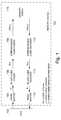
- FIG. 1is a schematic including a memory device, wherein the memory device stores data with an outer block code and a stream-based inner code.
- FIG. 2illustrates an example of a convolutional coder for the stream-based inner coding.
- FIG. 3is a schematic illustrating a memory device, wherein the memory device stores data with a stream-based code such that it effectively has a better (lower) bit error rate (BER) than if the stream-based code were not used.
- BERbit error rate
- FIG. 4is a schematic illustrating one embodiment of a memory device wherein data can be loaded in arbitrary order.
- FIG. 5is a schematic illustrating one embodiment of a memory device with relatively few components.
- FIG. 1is a schematic including a memory device 100 , wherein the memory device 100 stores data using an outer block code concatenated with a stream-based inner error correction code to generate a concatenated code.
- the stream-based inner error correction codeprocesses the data in streams or channels. Accordingly, the coding of the concatenated data is dependent on prior data received by the stream-based code coder.
- the stream-based codeis a convolutional code.
- the memory device 100is illustrated in communication with a CPU 102 , which represents another device using the memory device 100 .
- the CPU 102can correspond to a microprocessor, a controller, signal processor, or the like.
- the illustrated memory device 100includes a write buffer 104 , a block code coder 106 , a stream-based code coder 108 , a memory array 110 , a stream-based code decoder 112 , a block code decoder 114 , and a read buffer 116 .
- FIG. 3illustrates an alternative configuration with fewer functional blocks.
- the block code coder 106 and the stream-based code coder 108are each forward error correction (FEC) coders.
- FECforward error correction
- the memory array 110corresponds to a NAND flash memory array.
- the NAND flash memory arraycan be of single level, multi-level, or can even correspond to multiple arrays. While particular embodiments will be described in the context of NAND flash memory, the principles and advantages described herein are applicable to other types of memories.
- a very wide range of non-volatile solid state memory typescan be used for the memory array 110 .
- the memory array 110can correspond to other forms of flash (e.g., NOR type), electrically erasable programmable read only memory (EEPROM), magnetoresistive random access memory (MRAM), programmable conductor memory, ferroelectric memory, and the like.
- the block code coder 106generates the outer block code.
- the stream-based code coder 108generates the inner stream-based code, e.g., convolutional code.
- the stream-based code decoder 112decodes the inner stream-based code
- the block code decoder 114decodes the outer block code.
- the concatenation of the outer block code and the inner stream-based codeimproves the integrity of the stored data and increases the likelihood of recovering correctable data.
- the use of the inner stream-based codecan lower the bit error rate (BER) associated with the memory device 100 .
- the reduction in the BERis observed by the device using the memory device 100 , such as a host or the CPU 102 .
- the CPU 102 or controllerprovides data to the write buffer 104 for storage to the memory array 110 .
- a page of datais written to the memory array 110 at a time.
- This page of datacan vary in size. Typical page sizes include, but are not limited to, 512 bytes, 1024 bytes, 2048 bytes, and the like.
- a variable Nrepresents the number of bytes for a page.
- This N number of bytesis encoded by the block code coder 106 .
- block codesinclude, but are not limited to, a Hamming code, a Reed-Solomon error correction code, a Bose, Chaudhuri, Hocquenghem (BCH) code, or the like. Within limits, these block error correction codes can detect and correct many errors in the data.
- the error correction codes from the block codesoccupy additional bytes represented in FIG. 1 as variable y number of block code bytes. In a conventional NAND flash memory array, the block codes are typically stored in a spare bytes area for the corresponding page. For the purposes of illustration, these possible extra bytes are included in the variable y.
- N+y bytesare stored for the page for data and for error correction data.
- the type of block code used and the number of error correction bytes yare typically specified for a particular device by an applicable industry standard, such as by a JEDEC standard.
- the N bytes of the N+y bytesremain the same data, and the y block code bytes for error correction are appended to the data.
- the N bytescan be considered the original data for the block code coder 106
- the N+y bytescan be considered the original data for the stream-based coder 108 .
- the stream-based code coder 108performs a stream-based coding process on the N+y bytes of data.
- the stream-based codingincreases the amount of data stored by a factor z such that z(N+y) bytes are stored in the memory array 110 for the concatenated page of data.
- the resulting z(N+y) bytesare typically unique from the original N or N+y bytes of data, i.e., the N or N+y bytes of data are not recognizable without decoding. This can render decoding relatively difficult as compared to decoding of block codes.
- techniquessuch as the Viterbi algorithm can be used to decode convolutional codes in a relatively efficient manner.
- This factor zcan vary.
- the code rate (m/n) and the constraint length k for a convolutional codecan affect the size of the factor z.
- the factor zcan vary in a very broad range, but will be greater than 1.
- the stream-based codeis a convolutional code
- the factor zis 2.
- a simple convolutional coding examplewill be described later in connection with FIG. 2 , with a factor z of 2.
- the stream-based code decoder 112decodes, e.g., deconvolves, the stream-based coded z(N+y) bytes to N+y block-coded bytes. Within limits of the code, the decoding process detects and corrects errors.
- the stream-based code decoder 112is a Viterbi decoder (for decoding of convolutional codes).
- this extra stream-based codingreduces the number of errors, if any, in the resulting block-coded N+y bytes and improves the probability that the block-coded N+y bytes will be correctable.
- the block code decoder 114decodes the z(N+y) bytes of block-coded data and generates N bytes of corrected data (unless the errors are uncorrectable).
- the N bytes of corrected dataare placed in the read buffer 116 for access by the CPU 102 .
- FIG. 2illustrates an example of a convolutional coder 202 for the inner stream-based coding. While illustrated in the context of convolutional codes, the principles and advantages are applicable to other types of codes.
- Stream-based codingcan be performed by hardware or by software (or firmware as applicable), or by a combination of both. In one embodiment, stream-based coding is performed by dedicated hardware integrated with the memory device 100 or by a controller outside of the memory device 100 .
- the particular convolutional coder 202 illustrated in FIG. 2is a simple example of convolutional coding and is not intended to be limiting. An implementation of convolutional coding can vary widely with respect to many parameters, such as, but not limited to, constraint lengths, generator polynomials, and the like.
- Data 204indicates the N+y bytes of data from the block code coder 106 that would normally be stored in a conventional memory device.
- Data 206indicates the convolutional coded z(N+y) bytes of data generated by convolution coding of data 204 .
- data 204is convolved using a register 208 and an exclusive-OR (XOR) gate 210 .
- XORexclusive-OR
- the register 208can be initialized to zero for the first data bit (first memory cell of the string), or can be initialized to one.
- FIG. 3is a schematic illustrating a memory device 302 , wherein the memory device 302 stores data with a stream-based code such that it effectively has a better (lower) bit error rate (BER) than if the stream-based code were not used.
- the groupings of the components illustrated in FIG. 3vary from the grouping in FIG. 1 . The groupings can vary depending on the specifications for the memory devices 100 , 302 , depending on whether the memory devices 100 , 302 are provided at the die level or packaged, and the like.
- the memory device 302is operatively coupled to a controller 304 , which is in communication with a host 306 .
- the host 306 and the controller 304can be of a legacy specification.
- the controller 304can be part of the host 306 or can be part of the memory device 302 .
- some memory card formatsspecify the controller 304 to be onboard the memory device 302
- other formatsspecify the controller 304 to be part of the host 306 .
- the memory device 302includes the stream-based code coder 108 , the memory array 110 , and the stream-based code decoder 112 . These components were described earlier in connection with FIG. 1 .
- the controller 304includes the write buffer 104 , the block code coder 106 , the block code decoder 114 , and the read buffer 116 . These components were also described earlier in connection with FIG. 1 .
- One of ordinary skill in the artwill appreciate that other components, such as buffers, cache registers, address data, multiplexing/demultiplexing components, serializing/deserializing components, and control components can also be present as applicable. Further details of possible configurations for the memory device 302 will be described later in connection with FIGS. 4 and 5 .
- the difference in density between a relatively new memory array and a relatively old memory arraycan be fairly dramatic.
- the geometry feature size of a relatively new memory arrayis about 1 ⁇ 3 of that of a relatively old memory array. This increases the chip density by a factor of about 10.
- the individual memory cellsshrink, they also typically become individually less reliable and more susceptible to noise. This can render relatively new memory devices with small geometry unusable with the legacy specifications.
- the relatively small geometry deviceswould typically fail the bit error rate (BER) specification.
- BERbit error rate
- One embodimenttransparently applies the inner stream-based code to the block-coded data such that a host is unaware that a stream-based code is being used.
- Thisadvantageously permits a relatively new and low-cost memory device to meet the bit error rate (BER) requirements while outwardly using only the block coded data specified for a legacy device. For example, even if half of the memory capacity were to be used, a small-geometry memory device of about 10 times the density would still be about 5 times more dense and thus cheaper than a larger-geometry device. This can further permit a manufacturer to build products for a wider range of product lines from relatively fewer production lines.
- BERbit error rate
- FIG. 4is a schematic illustrating one embodiment of the memory device 302 wherein data can be loaded in arbitrary order.
- the memory device 302includes a first page latch 402 and a second page latch 404 .
- the second page latch 404stores a page of data received from an interface.
- the second page latch 404accumulates this data so that the stream-based code coder 108 can process the forward error correction coded data of the stream-based coding operation.
- the correction coding of datadepends on earlier values of data.
- the stream-based code coder 108initiates the coding process after the page of data has been loaded into the second page latch 404 .
- An indicationsuch as a “program page” signal can be used to indicate the readiness of the data.
- the program page signalfrom the host 306 or controller 304 ( FIG. 3 ) initiates the storage into the array. It will be understood that for flash memory devices, the applicable portion of the array may need to be erased prior to programming.
- the program page signalis used to initiate the additional error correction by the stream-based code coder 108 , and when the coding is complete, the stream-based code coder 108 initiates the programming of data from the first page latch 402 to the memory array 110 .
- the second page latch 404typically stores N+y data bytes.
- the memory device 302can receive the data bytes for the page without a specific order.
- the stream-based code coder 108encodes the N+y data bytes to the z(N+y) bytes with stream-based coding, such as convolutional coding. These z(N+y) bytes are stored in the first page latch 402 for writing to the memory array 110 .
- FIG. 5is a schematic illustrating one embodiment of the memory device 302 with relatively fewer components.
- the data from the interfaceis not stored in a page latch prior to encoding.
- a smaller latch or registersmall than a page is used instead. This can reduce cost.
- the computation of some codes, such as convolutional codesis dependent on prior values of data. Accordingly, without the second page latch 404 , the data from an interface may need to be provided in such an order that the stream-based code coder 108 can process the inner error correction code.
- One embodimentis an apparatus, wherein the apparatus includes: one or more memory arrays for storage of data; a stream-based coder configured to generate a page of forward error correction coded data of a page of original data intended for storage in the one or more memory arrays such that the coded page of data is larger than the page of original data and such that the original data is not recognizable in the coded data without decoding the coded data; a page latch operatively coupled to the stream-based coder, wherein the page latch is at least large enough to hold the page of coded data for writing to the one or more memory arrays; and a stream-based decoder configured to decode coded data retrieved from the one or more memory arrays to generate decoded data.
- One embodimentis a method for storing data in a device having one or more memory arrays, wherein the method includes: receiving block-coded data for storage in the one or more memory arrays; concatenating the block-coded data with a forward error correction code to generate a concatenated code that is larger in size than the original block-coded data; and storing the concatenated code in the one or more memory arrays.
- One embodimentis a method of retrieving a first data stored in a memory device, wherein the method includes: receiving a request for the first data; retrieving a concatenated data from one or more memory arrays, wherein the concatenated data corresponds to the first data and a first block code of the first data concatenated with a second forward error correction code; and decoding the concatenated data to generate the first data and block codes.
Landscapes
- Engineering & Computer Science (AREA)
- Theoretical Computer Science (AREA)
- Quality & Reliability (AREA)
- Physics & Mathematics (AREA)
- General Engineering & Computer Science (AREA)
- General Physics & Mathematics (AREA)
- Techniques For Improving Reliability Of Storages (AREA)
- Detection And Correction Of Errors (AREA)
- Error Detection And Correction (AREA)
Abstract
Description
Claims (10)
Priority Applications (5)
| Application Number | Priority Date | Filing Date | Title |
|---|---|---|---|
| US11/774,377US8065583B2 (en) | 2007-07-06 | 2007-07-06 | Data storage with an outer block code and a stream-based inner code |
| PCT/US2008/068240WO2009009303A2 (en) | 2007-07-06 | 2008-06-25 | Data storage with an outer block code and a stream-based inner code |
| TW097125483ATW200919481A (en) | 2007-07-06 | 2008-07-04 | Data storage with an outer block code and a stream-based inner code |
| US13/281,007US8239725B2 (en) | 2007-07-06 | 2011-10-25 | Data storage with an outer block code and a stream-based inner code |
| US14/263,825US9063875B2 (en) | 2007-07-06 | 2014-04-28 | Error recovery storage along a memory string |
Applications Claiming Priority (1)
| Application Number | Priority Date | Filing Date | Title |
|---|---|---|---|
| US11/774,377US8065583B2 (en) | 2007-07-06 | 2007-07-06 | Data storage with an outer block code and a stream-based inner code |
Related Child Applications (1)
| Application Number | Title | Priority Date | Filing Date |
|---|---|---|---|
| US13/281,007ContinuationUS8239725B2 (en) | 2007-07-06 | 2011-10-25 | Data storage with an outer block code and a stream-based inner code |
Publications (2)
| Publication Number | Publication Date |
|---|---|
| US20090013234A1 US20090013234A1 (en) | 2009-01-08 |
| US8065583B2true US8065583B2 (en) | 2011-11-22 |
Family
ID=40222374
Family Applications (2)
| Application Number | Title | Priority Date | Filing Date |
|---|---|---|---|
| US11/774,377Active2030-09-20US8065583B2 (en) | 2007-07-06 | 2007-07-06 | Data storage with an outer block code and a stream-based inner code |
| US13/281,007ActiveUS8239725B2 (en) | 2007-07-06 | 2011-10-25 | Data storage with an outer block code and a stream-based inner code |
Family Applications After (1)
| Application Number | Title | Priority Date | Filing Date |
|---|---|---|---|
| US13/281,007ActiveUS8239725B2 (en) | 2007-07-06 | 2011-10-25 | Data storage with an outer block code and a stream-based inner code |
Country Status (3)
| Country | Link |
|---|---|
| US (2) | US8065583B2 (en) |
| TW (1) | TW200919481A (en) |
| WO (1) | WO2009009303A2 (en) |
Cited By (74)
| Publication number | Priority date | Publication date | Assignee | Title |
|---|---|---|---|---|
| US20090043951A1 (en)* | 2007-08-06 | 2009-02-12 | Anobit Technologies Ltd. | Programming schemes for multi-level analog memory cells |
| US20090129169A1 (en)* | 2007-11-21 | 2009-05-21 | Micron Technology, Inc. | Method and apparatus for reading data from flash memory |
| US20090144600A1 (en)* | 2007-11-30 | 2009-06-04 | Anobit Technologies Ltd | Efficient re-read operations from memory devices |
| US20100220509A1 (en)* | 2009-03-01 | 2010-09-02 | Anobit Technologies Ltd | Selective Activation of Programming Schemes in Analog Memory Cell Arrays |
| US20100251076A1 (en)* | 2009-03-27 | 2010-09-30 | Chao-Yi Wu | Storage controller having soft decoder included therein, related storage control method thereof and system using the same |
| US8208304B2 (en) | 2008-11-16 | 2012-06-26 | Anobit Technologies Ltd. | Storage at M bits/cell density in N bits/cell analog memory cell devices, M>N |
| US8209588B2 (en) | 2007-12-12 | 2012-06-26 | Anobit Technologies Ltd. | Efficient interference cancellation in analog memory cell arrays |
| US8230300B2 (en) | 2008-03-07 | 2012-07-24 | Apple Inc. | Efficient readout from analog memory cells using data compression |
| US8234545B2 (en) | 2007-05-12 | 2012-07-31 | Apple Inc. | Data storage with incremental redundancy |
| US8239734B1 (en)* | 2008-10-15 | 2012-08-07 | Apple Inc. | Efficient data storage in storage device arrays |
| US8238157B1 (en) | 2009-04-12 | 2012-08-07 | Apple Inc. | Selective re-programming of analog memory cells |
| US8239735B2 (en) | 2006-05-12 | 2012-08-07 | Apple Inc. | Memory Device with adaptive capacity |
| US8248831B2 (en) | 2008-12-31 | 2012-08-21 | Apple Inc. | Rejuvenation of analog memory cells |
| US8259506B1 (en) | 2009-03-25 | 2012-09-04 | Apple Inc. | Database of memory read thresholds |
| US8261159B1 (en) | 2008-10-30 | 2012-09-04 | Apple, Inc. | Data scrambling schemes for memory devices |
| US8270246B2 (en) | 2007-11-13 | 2012-09-18 | Apple Inc. | Optimized selection of memory chips in multi-chips memory devices |
| US8300478B2 (en) | 2007-09-19 | 2012-10-30 | Apple Inc. | Reducing distortion using joint storage |
| US8369141B2 (en) | 2007-03-12 | 2013-02-05 | Apple Inc. | Adaptive estimation of memory cell read thresholds |
| US8386895B2 (en) | 2010-05-19 | 2013-02-26 | Micron Technology, Inc. | Enhanced multilevel memory |
| US8397131B1 (en) | 2008-12-31 | 2013-03-12 | Apple Inc. | Efficient readout schemes for analog memory cell devices |
| US8400858B2 (en) | 2008-03-18 | 2013-03-19 | Apple Inc. | Memory device with reduced sense time readout |
| US8429493B2 (en) | 2007-05-12 | 2013-04-23 | Apple Inc. | Memory device with internal signap processing unit |
| US8437185B2 (en) | 2007-09-19 | 2013-05-07 | Apple Inc. | Programming orders for reducing distortion based on neighboring rows |
| US8456905B2 (en) | 2007-12-16 | 2013-06-04 | Apple Inc. | Efficient data storage in multi-plane memory devices |
| US8479080B1 (en) | 2009-07-12 | 2013-07-02 | Apple Inc. | Adaptive over-provisioning in memory systems |
| US8482978B1 (en) | 2008-09-14 | 2013-07-09 | Apple Inc. | Estimation of memory cell read thresholds by sampling inside programming level distribution intervals |
| US8495465B1 (en) | 2009-10-15 | 2013-07-23 | Apple Inc. | Error correction coding over multiple memory pages |
| US8493783B2 (en) | 2008-03-18 | 2013-07-23 | Apple Inc. | Memory device readout using multiple sense times |
| US8493781B1 (en) | 2010-08-12 | 2013-07-23 | Apple Inc. | Interference mitigation using individual word line erasure operations |
| US8498151B1 (en) | 2008-08-05 | 2013-07-30 | Apple Inc. | Data storage in analog memory cells using modified pass voltages |
| US8527819B2 (en) | 2007-10-19 | 2013-09-03 | Apple Inc. | Data storage in analog memory cell arrays having erase failures |
| US8572311B1 (en) | 2010-01-11 | 2013-10-29 | Apple Inc. | Redundant data storage in multi-die memory systems |
| US8570804B2 (en) | 2006-05-12 | 2013-10-29 | Apple Inc. | Distortion estimation and cancellation in memory devices |
| US8572423B1 (en) | 2010-06-22 | 2013-10-29 | Apple Inc. | Reducing peak current in memory systems |
| US8595573B2 (en) | 2006-12-03 | 2013-11-26 | Apple Inc. | Automatic defect management in memory devices |
| US8595591B1 (en) | 2010-07-11 | 2013-11-26 | Apple Inc. | Interference-aware assignment of programming levels in analog memory cells |
| US8645794B1 (en) | 2010-07-31 | 2014-02-04 | Apple Inc. | Data storage in analog memory cells using a non-integer number of bits per cell |
| US8677054B1 (en) | 2009-12-16 | 2014-03-18 | Apple Inc. | Memory management schemes for non-volatile memory devices |
| US8694854B1 (en) | 2010-08-17 | 2014-04-08 | Apple Inc. | Read threshold setting based on soft readout statistics |
| US8694814B1 (en) | 2010-01-10 | 2014-04-08 | Apple Inc. | Reuse of host hibernation storage space by memory controller |
| US8694853B1 (en) | 2010-05-04 | 2014-04-08 | Apple Inc. | Read commands for reading interfering memory cells |
| US8788910B1 (en) | 2012-05-22 | 2014-07-22 | Pmc-Sierra, Inc. | Systems and methods for low latency, high reliability error correction in a flash drive |
| US8793556B1 (en) | 2012-05-22 | 2014-07-29 | Pmc-Sierra, Inc. | Systems and methods for reclaiming flash blocks of a flash drive |
| US8832354B2 (en) | 2009-03-25 | 2014-09-09 | Apple Inc. | Use of host system resources by memory controller |
| US8856475B1 (en) | 2010-08-01 | 2014-10-07 | Apple Inc. | Efficient selection of memory blocks for compaction |
| US8924661B1 (en) | 2009-01-18 | 2014-12-30 | Apple Inc. | Memory system including a controller and processors associated with memory devices |
| US8949684B1 (en) | 2008-09-02 | 2015-02-03 | Apple Inc. | Segmented data storage |
| US8972824B1 (en) | 2012-05-22 | 2015-03-03 | Pmc-Sierra, Inc. | Systems and methods for transparently varying error correction code strength in a flash drive |
| US8996957B1 (en) | 2012-05-22 | 2015-03-31 | Pmc-Sierra, Inc. | Systems and methods for initializing regions of a flash drive having diverse error correction coding (ECC) schemes |
| US9009565B1 (en) | 2013-03-15 | 2015-04-14 | Pmc-Sierra, Inc. | Systems and methods for mapping for solid-state memory |
| US9021337B1 (en) | 2012-05-22 | 2015-04-28 | Pmc-Sierra, Inc. | Systems and methods for adaptively selecting among different error correction coding schemes in a flash drive |
| US9021181B1 (en) | 2010-09-27 | 2015-04-28 | Apple Inc. | Memory management for unifying memory cell conditions by using maximum time intervals |
| US9021336B1 (en) | 2012-05-22 | 2015-04-28 | Pmc-Sierra, Inc. | Systems and methods for redundantly storing error correction codes in a flash drive with secondary parity information spread out across each page of a group of pages |
| US9021333B1 (en) | 2012-05-22 | 2015-04-28 | Pmc-Sierra, Inc. | Systems and methods for recovering data from failed portions of a flash drive |
| US9026867B1 (en) | 2013-03-15 | 2015-05-05 | Pmc-Sierra, Inc. | Systems and methods for adapting to changing characteristics of multi-level cells in solid-state memory |
| US9047214B1 (en) | 2012-05-22 | 2015-06-02 | Pmc-Sierra, Inc. | System and method for tolerating a failed page in a flash device |
| US9053012B1 (en) | 2013-03-15 | 2015-06-09 | Pmc-Sierra, Inc. | Systems and methods for storing data for solid-state memory |
| US9053047B2 (en) | 2012-08-27 | 2015-06-09 | Apple Inc. | Parameter estimation using partial ECC decoding |
| US9065483B2 (en) | 2013-01-21 | 2015-06-23 | Micron Technology, Inc. | Determining soft data using a classification code |
| US9081701B1 (en) | 2013-03-15 | 2015-07-14 | Pmc-Sierra, Inc. | Systems and methods for decoding data for solid-state memory |
| US9104580B1 (en) | 2010-07-27 | 2015-08-11 | Apple Inc. | Cache memory for hybrid disk drives |
| US9116822B2 (en) | 2012-12-07 | 2015-08-25 | Micron Technology, Inc. | Stopping criteria for layered iterative error correction |
| US9171624B2 (en) | 2013-12-20 | 2015-10-27 | Apple Inc. | Management of data storage in analog memory cells using a non-integer number of bits per cell |
| US9176812B1 (en) | 2012-05-22 | 2015-11-03 | Pmc-Sierra, Inc. | Systems and methods for storing data in page stripes of a flash drive |
| US9183085B1 (en) | 2012-05-22 | 2015-11-10 | Pmc-Sierra, Inc. | Systems and methods for adaptively selecting from among a plurality of error correction coding schemes in a flash drive for robustness and low latency |
| US9208018B1 (en) | 2013-03-15 | 2015-12-08 | Pmc-Sierra, Inc. | Systems and methods for reclaiming memory for solid-state memory |
| US9229848B2 (en) | 2013-01-21 | 2016-01-05 | Micron Technology, Inc. | Determining soft data for fractional digit memory cells |
| US9577673B2 (en) | 2012-11-08 | 2017-02-21 | Micron Technology, Inc. | Error correction methods and apparatuses using first and second decoders |
| US9740559B2 (en) | 2015-10-28 | 2017-08-22 | Avago Technologies General Ip (Singapore) Pte. Ltd. | Systems and methods for compaction based flash memory data recovery |
| US10108489B2 (en) | 2015-10-28 | 2018-10-23 | Avago Technologies General Ip (Singapore) Pte. Ltd. | Systems and methods for efficient soft data based flash memory data recovery |
| US10204006B2 (en) | 2015-10-28 | 2019-02-12 | Avago Technologies International Sales Pte. Limited | Systems and methods for side data based soft data flash memory access |
| US10291261B2 (en) | 2016-04-25 | 2019-05-14 | SK Hynix Inc. | Early selection decoding and automatic tuning |
| US11556416B2 (en) | 2021-05-05 | 2023-01-17 | Apple Inc. | Controlling memory readout reliability and throughput by adjusting distance between read thresholds |
| US11847342B2 (en) | 2021-07-28 | 2023-12-19 | Apple Inc. | Efficient transfer of hard data and confidence levels in reading a nonvolatile memory |
Families Citing this family (21)
| Publication number | Priority date | Publication date | Assignee | Title |
|---|---|---|---|---|
| US8051358B2 (en) | 2007-07-06 | 2011-11-01 | Micron Technology, Inc. | Error recovery storage along a nand-flash string |
| US8327245B2 (en) | 2007-11-21 | 2012-12-04 | Micron Technology, Inc. | Memory controller supporting rate-compatible punctured codes |
| US8046542B2 (en)* | 2007-11-21 | 2011-10-25 | Micron Technology, Inc. | Fault-tolerant non-volatile integrated circuit memory |
| US8230158B2 (en) | 2008-08-12 | 2012-07-24 | Micron Technology, Inc. | Memory devices and methods of storing data on a memory device |
| US8751860B2 (en)* | 2009-06-03 | 2014-06-10 | Micron Technology, Inc. | Object oriented memory in solid state devices |
| EP2299362A3 (en)* | 2009-08-18 | 2011-05-04 | ViaSat, Inc. | Forward error correction for memories |
| US8271697B2 (en) | 2009-09-29 | 2012-09-18 | Micron Technology, Inc. | State change in systems having devices coupled in a chained configuration |
| KR101678053B1 (en) | 2010-04-02 | 2016-11-22 | 삼성전자 주식회사 | Semiconductor device and decoding method thereof |
| US8429391B2 (en) | 2010-04-16 | 2013-04-23 | Micron Technology, Inc. | Boot partitions in memory devices and systems |
| US8451664B2 (en) | 2010-05-12 | 2013-05-28 | Micron Technology, Inc. | Determining and using soft data in memory devices and systems |
| US8572457B2 (en) | 2010-05-28 | 2013-10-29 | Seagate Technology Llc | Outer code protection for solid state memory devices |
| KR101944793B1 (en)* | 2012-09-04 | 2019-02-08 | 삼성전자주식회사 | Flash memory system including flash memory and detecting method of abnormal wordline thereof |
| CN103064640B (en)* | 2012-12-31 | 2015-11-18 | 苏州国芯科技有限公司 | Fast reading and writing method applied to nandflash storage device |
| CN104599717B (en)* | 2012-12-31 | 2017-11-24 | 苏州国芯科技有限公司 | NAND Flash memory data storage method with error correction |
| CN104598169B (en)* | 2012-12-31 | 2018-02-09 | 苏州国芯科技有限公司 | High reliability data read method for flash memory |
| US9559725B1 (en) | 2013-10-23 | 2017-01-31 | Seagate Technology Llc | Multi-strength reed-solomon outer code protection |
| US9396062B1 (en) | 2014-04-04 | 2016-07-19 | Seagate Technology Llc | Group based codes for multi-dimensional recording (MDR) |
| US9912355B2 (en)* | 2015-09-25 | 2018-03-06 | Intel Corporation | Distributed concatenated error correction |
| US10614903B2 (en) | 2016-07-18 | 2020-04-07 | International Business Machines Corporation | Testing non-volatile memories |
| US10388351B2 (en) | 2017-08-30 | 2019-08-20 | Micron Technology, Inc. | Wear leveling for random access and ferroelectric memory |
| US11507614B1 (en) | 2018-02-13 | 2022-11-22 | Snap Inc. | Icon based tagging |
Citations (29)
| Publication number | Priority date | Publication date | Assignee | Title |
|---|---|---|---|---|
| US5942004A (en) | 1994-10-31 | 1999-08-24 | Stmicroelectronics, S.R.L. | Device and a method for storing data and corresponding error-correction information |
| US5956743A (en) | 1997-08-25 | 1999-09-21 | Bit Microsystems, Inc. | Transparent management at host interface of flash-memory overhead-bytes using flash-specific DMA having programmable processor-interrupt of high-level operations |
| US6023781A (en) | 1996-09-18 | 2000-02-08 | Nippon Steel Corporation | Multilevel semiconductor memory, write/read method thereto/therefrom and storage medium storing write/read program |
| JP2000149592A (en) | 1998-11-11 | 2000-05-30 | Nec Ic Microcomput Syst Ltd | Memory cell for defect relief and storage device utilizing the same |
| US6279133B1 (en) | 1997-12-31 | 2001-08-21 | Kawasaki Steel Corporation | Method and apparatus for significantly improving the reliability of multilevel memory architecture |
| US20020120820A1 (en)* | 2001-02-28 | 2002-08-29 | Fujitsu Limited | Memory device for controlling nonvolatile and volatile memories |
| US6591394B2 (en) | 2000-12-22 | 2003-07-08 | Matrix Semiconductor, Inc. | Three-dimensional memory array and method for storing data bits and ECC bits therein |
| US6732322B1 (en) | 1998-01-21 | 2004-05-04 | Sony Corporation | Encoding method and memory device |
| US6731538B2 (en) | 2000-03-10 | 2004-05-04 | Kabushiki Kaisha Toshiba | Semiconductor memory device including page latch circuit |
| US6839870B2 (en) | 2003-03-21 | 2005-01-04 | Terayon Communications Systems, Inc. | Error-correcting code interleaver |
| US6871303B2 (en) | 1998-12-04 | 2005-03-22 | Qualcomm Incorporated | Random-access multi-directional CDMA2000 turbo code interleaver |
| US6895543B2 (en) | 1996-09-18 | 2005-05-17 | Nippon Steel Corporation | Multilevel semiconductor memory, write/read method thereto/therefrom and storage medium storing write/read program |
| US20050114587A1 (en) | 2003-11-22 | 2005-05-26 | Super Talent Electronics Inc. | ExpressCard with On-Card Flash Memory with Shared Flash-Control Bus but Separate Ready Lines |
| WO2006070668A1 (en) | 2004-12-28 | 2006-07-06 | International Business Machines Corporation | Information recording device, data-flow controller for the device, and control method for the data-flow |
| US20060221752A1 (en) | 2005-03-31 | 2006-10-05 | Fasoli Luca G | Integrated circuit memory array configuration including decoding compatibility with partial implementation of multiple memory layers |
| US7184356B2 (en) | 2003-07-31 | 2007-02-27 | Kabushiki Kaisha Toshiba | Semiconductor memory device |
| US20070171714A1 (en) | 2006-01-20 | 2007-07-26 | Marvell International Ltd. | Flash memory with coding and signal processing |
| US20070171730A1 (en) | 2006-01-20 | 2007-07-26 | Marvell International Ltd. | Method and system for error correction in flash memory |
| KR100766042B1 (en) | 2006-12-06 | 2007-10-12 | 삼성전자주식회사 | Multilevel Cell Memory Device Using Concatenated Coding |
| US20070266296A1 (en)* | 2006-05-15 | 2007-11-15 | Conley Kevin M | Nonvolatile Memory with Convolutional Coding |
| US20080163023A1 (en) | 2007-01-03 | 2008-07-03 | Si-Hoon Hong | ECC controller for use in flash memory device and memory system including the same |
| US20080168319A1 (en)* | 2007-01-08 | 2008-07-10 | Samsung Electronics Co., Ltd. | Flash memory Device Error Correction Code Controllers and Related Methods and Memory Systems |
| US20090013233A1 (en) | 2007-07-06 | 2009-01-08 | Micron Technology, Inc. | Error recovery storage along a nand-flash string |
| US7478314B1 (en)* | 2004-08-04 | 2009-01-13 | Marvell International Ltd. | Methods, algorithms, software, circuits, receivers and system for decoding convolutional code |
| US20090100307A1 (en)* | 2004-08-30 | 2009-04-16 | Silicon Storage Technology, Inc. | Systems and methods for providing nonvolatile memory management in wireless phones |
| US7643342B2 (en) | 2006-03-06 | 2010-01-05 | Ramot At Tel-Aviv University Ltd. | Multi-bit-per-cell flash memory device with non-bijective mapping |
| US20100023800A1 (en)* | 2005-09-26 | 2010-01-28 | Eliyahou Harari | NAND Flash Memory Controller Exporting a NAND Interface |
| US20100115376A1 (en)* | 2006-12-03 | 2010-05-06 | Anobit Technologies Ltd. | Automatic defect management in memory devices |
| US7904780B2 (en) | 2006-11-03 | 2011-03-08 | Sandisk Corporation | Methods of modulating error correction coding |
Family Cites Families (11)
| Publication number | Priority date | Publication date | Assignee | Title |
|---|---|---|---|---|
| US4058851A (en) | 1976-10-18 | 1977-11-15 | Sperry Rand Corporation | Conditional bypass of error correction for dual memory access time selection |
| US6628723B1 (en) | 1999-10-15 | 2003-09-30 | Cisco Technology | Coding rate reduction for turbo codes |
| US6683817B2 (en) | 2002-02-21 | 2004-01-27 | Qualcomm, Incorporated | Direct memory swapping between NAND flash and SRAM with error correction coding |
| US7293217B2 (en) | 2002-12-16 | 2007-11-06 | Interdigital Technology Corporation | Detection, avoidance and/or correction of problematic puncturing patterns in parity bit streams used when implementing turbo codes |
| US7467264B2 (en) | 2003-06-27 | 2008-12-16 | Hewlett-Packard Development Company, L.P. | Methods and apparatuses for determining the state of a memory element |
| US7389465B2 (en) | 2004-01-30 | 2008-06-17 | Micron Technology, Inc. | Error detection and correction scheme for a memory device |
| US7061804B2 (en) | 2004-11-18 | 2006-06-13 | Qualcomm Incorporated | Robust and high-speed memory access with adaptive interface timing |
| US7644338B2 (en) | 2005-09-13 | 2010-01-05 | Samsung Electronics Co., Ltd. | Method of detecting and correcting a prescribed set of error events based on error detecting code |
| US7469368B2 (en) | 2005-11-29 | 2008-12-23 | Broadcom Corporation | Method and system for a non-volatile memory with multiple bits error correction and detection for improving production yield |
| US7840875B2 (en) | 2006-05-15 | 2010-11-23 | Sandisk Corporation | Convolutional coding methods for nonvolatile memory |
| US8046660B2 (en) | 2006-08-07 | 2011-10-25 | Marvell World Trade Ltd. | System and method for correcting errors in non-volatile memory using product codes |
- 2007
- 2007-07-06USUS11/774,377patent/US8065583B2/enactiveActive
- 2008
- 2008-06-25WOPCT/US2008/068240patent/WO2009009303A2/enactiveApplication Filing
- 2008-07-04TWTW097125483Apatent/TW200919481A/enunknown
- 2011
- 2011-10-25USUS13/281,007patent/US8239725B2/enactiveActive
Patent Citations (34)
| Publication number | Priority date | Publication date | Assignee | Title |
|---|---|---|---|---|
| US5942004A (en) | 1994-10-31 | 1999-08-24 | Stmicroelectronics, S.R.L. | Device and a method for storing data and corresponding error-correction information |
| US6023781A (en) | 1996-09-18 | 2000-02-08 | Nippon Steel Corporation | Multilevel semiconductor memory, write/read method thereto/therefrom and storage medium storing write/read program |
| US6895543B2 (en) | 1996-09-18 | 2005-05-17 | Nippon Steel Corporation | Multilevel semiconductor memory, write/read method thereto/therefrom and storage medium storing write/read program |
| US5956743A (en) | 1997-08-25 | 1999-09-21 | Bit Microsystems, Inc. | Transparent management at host interface of flash-memory overhead-bytes using flash-specific DMA having programmable processor-interrupt of high-level operations |
| US6279133B1 (en) | 1997-12-31 | 2001-08-21 | Kawasaki Steel Corporation | Method and apparatus for significantly improving the reliability of multilevel memory architecture |
| US6732322B1 (en) | 1998-01-21 | 2004-05-04 | Sony Corporation | Encoding method and memory device |
| JP2000149592A (en) | 1998-11-11 | 2000-05-30 | Nec Ic Microcomput Syst Ltd | Memory cell for defect relief and storage device utilizing the same |
| US6871303B2 (en) | 1998-12-04 | 2005-03-22 | Qualcomm Incorporated | Random-access multi-directional CDMA2000 turbo code interleaver |
| US6731538B2 (en) | 2000-03-10 | 2004-05-04 | Kabushiki Kaisha Toshiba | Semiconductor memory device including page latch circuit |
| US6591394B2 (en) | 2000-12-22 | 2003-07-08 | Matrix Semiconductor, Inc. | Three-dimensional memory array and method for storing data bits and ECC bits therein |
| US20020120820A1 (en)* | 2001-02-28 | 2002-08-29 | Fujitsu Limited | Memory device for controlling nonvolatile and volatile memories |
| US6839870B2 (en) | 2003-03-21 | 2005-01-04 | Terayon Communications Systems, Inc. | Error-correcting code interleaver |
| US7184356B2 (en) | 2003-07-31 | 2007-02-27 | Kabushiki Kaisha Toshiba | Semiconductor memory device |
| US20050114587A1 (en) | 2003-11-22 | 2005-05-26 | Super Talent Electronics Inc. | ExpressCard with On-Card Flash Memory with Shared Flash-Control Bus but Separate Ready Lines |
| US7478314B1 (en)* | 2004-08-04 | 2009-01-13 | Marvell International Ltd. | Methods, algorithms, software, circuits, receivers and system for decoding convolutional code |
| US20090100307A1 (en)* | 2004-08-30 | 2009-04-16 | Silicon Storage Technology, Inc. | Systems and methods for providing nonvolatile memory management in wireless phones |
| WO2006070668A1 (en) | 2004-12-28 | 2006-07-06 | International Business Machines Corporation | Information recording device, data-flow controller for the device, and control method for the data-flow |
| US20080320361A1 (en) | 2004-12-28 | 2008-12-25 | Junichi Fukuda | Information Recording Device, Data-Flow Controller and Data Flow Controlling Method |
| US20060221752A1 (en) | 2005-03-31 | 2006-10-05 | Fasoli Luca G | Integrated circuit memory array configuration including decoding compatibility with partial implementation of multiple memory layers |
| US20100023800A1 (en)* | 2005-09-26 | 2010-01-28 | Eliyahou Harari | NAND Flash Memory Controller Exporting a NAND Interface |
| US20070171714A1 (en) | 2006-01-20 | 2007-07-26 | Marvell International Ltd. | Flash memory with coding and signal processing |
| US20070171730A1 (en) | 2006-01-20 | 2007-07-26 | Marvell International Ltd. | Method and system for error correction in flash memory |
| US20110060969A1 (en) | 2006-01-20 | 2011-03-10 | Marvell International Ltd. | Method and system for error correction in flash memory |
| US7844879B2 (en) | 2006-01-20 | 2010-11-30 | Marvell World Trade Ltd. | Method and system for error correction in flash memory |
| US7643342B2 (en) | 2006-03-06 | 2010-01-05 | Ramot At Tel-Aviv University Ltd. | Multi-bit-per-cell flash memory device with non-bijective mapping |
| US20070266296A1 (en)* | 2006-05-15 | 2007-11-15 | Conley Kevin M | Nonvolatile Memory with Convolutional Coding |
| US7904780B2 (en) | 2006-11-03 | 2011-03-08 | Sandisk Corporation | Methods of modulating error correction coding |
| US20100115376A1 (en)* | 2006-12-03 | 2010-05-06 | Anobit Technologies Ltd. | Automatic defect management in memory devices |
| KR100766042B1 (en) | 2006-12-06 | 2007-10-12 | 삼성전자주식회사 | Multilevel Cell Memory Device Using Concatenated Coding |
| US20080137414A1 (en) | 2006-12-06 | 2008-06-12 | Samsung Electronics Co., Ltd. | Multi-level cell memory device and method thereof |
| US7962831B2 (en)* | 2006-12-06 | 2011-06-14 | Samsung Electronics Co., Ltd. | Multi-level cell memory device and method thereof |
| US20080163023A1 (en) | 2007-01-03 | 2008-07-03 | Si-Hoon Hong | ECC controller for use in flash memory device and memory system including the same |
| US20080168319A1 (en)* | 2007-01-08 | 2008-07-10 | Samsung Electronics Co., Ltd. | Flash memory Device Error Correction Code Controllers and Related Methods and Memory Systems |
| US20090013233A1 (en) | 2007-07-06 | 2009-01-08 | Micron Technology, Inc. | Error recovery storage along a nand-flash string |
Non-Patent Citations (8)
| Title |
|---|
| International search report mailed Dec. 29, 2008 in PCT Application No. PCT/US2008/068240. |
| International search report mailed Jan. 20, 2009 in PCT Application No. PCT/US2008/068236. |
| Korean Intellectual Property Office; "Notification of Transmittal of the International Search Report and the Written Opinion of the International Searching Authority, or the Declaration", "Written Opinion of the International Searching Authority", and "International search report" of related International Application PCT/US2008/081743, filed Oct. 28, 2008; Dated Feb. 19, 2009; Daejeon, Republic of Korea. |
| Korean Intellectual Property Office; "Notification of Transmittal of the International Search Report and the Written Opinion of the International Searching Authority, or the Declaration", "Written Opinion of the International Searching Authority", and "International Search Report" of related PCT application PCT/US/2008/081475, filed Oct. 28, 2008; mailed Feb. 18, 2009; Daejeon, Republic of Korea. |
| The International Bureau of WIPO; International Preliminary Report on Patentability of related PCT Application No. PCT/US2008/068236, filed Jun. 25, 2008; mailing date Jan. 21, 2010; Geneva, Switzerland. |
| The International Bureau of WIPO; International Preliminary Report on Patentability of related PCT Application No. PCT/US2008/068240, filed Jun. 25, 2008; mailing date Jan. 21, 2010; Geneva, Switzerland. |
| USPTO; Office Action dated Dec. 9, 2010, from related application U.S. Appl. No. 11/944,023, filed Nov. 21, 2007. |
| USPTO; Office Action dated Sep. 9, 2010, from related application U.S. Appl. No. 11/944,023, filed Nov. 21, 2007. |
Cited By (99)
| Publication number | Priority date | Publication date | Assignee | Title |
|---|---|---|---|---|
| US8599611B2 (en) | 2006-05-12 | 2013-12-03 | Apple Inc. | Distortion estimation and cancellation in memory devices |
| US8239735B2 (en) | 2006-05-12 | 2012-08-07 | Apple Inc. | Memory Device with adaptive capacity |
| US8570804B2 (en) | 2006-05-12 | 2013-10-29 | Apple Inc. | Distortion estimation and cancellation in memory devices |
| US8595573B2 (en) | 2006-12-03 | 2013-11-26 | Apple Inc. | Automatic defect management in memory devices |
| US8369141B2 (en) | 2007-03-12 | 2013-02-05 | Apple Inc. | Adaptive estimation of memory cell read thresholds |
| US8429493B2 (en) | 2007-05-12 | 2013-04-23 | Apple Inc. | Memory device with internal signap processing unit |
| US8234545B2 (en) | 2007-05-12 | 2012-07-31 | Apple Inc. | Data storage with incremental redundancy |
| US20090043951A1 (en)* | 2007-08-06 | 2009-02-12 | Anobit Technologies Ltd. | Programming schemes for multi-level analog memory cells |
| US8259497B2 (en) | 2007-08-06 | 2012-09-04 | Apple Inc. | Programming schemes for multi-level analog memory cells |
| US8300478B2 (en) | 2007-09-19 | 2012-10-30 | Apple Inc. | Reducing distortion using joint storage |
| US8437185B2 (en) | 2007-09-19 | 2013-05-07 | Apple Inc. | Programming orders for reducing distortion based on neighboring rows |
| US8527819B2 (en) | 2007-10-19 | 2013-09-03 | Apple Inc. | Data storage in analog memory cell arrays having erase failures |
| US8270246B2 (en) | 2007-11-13 | 2012-09-18 | Apple Inc. | Optimized selection of memory chips in multi-chips memory devices |
| US9197251B2 (en) | 2007-11-21 | 2015-11-24 | Micron Technology, Inc. | Method and apparatus for reading data from non-volatile memory |
| US8499229B2 (en)* | 2007-11-21 | 2013-07-30 | Micro Technology, Inc. | Method and apparatus for reading data from flash memory |
| US8719680B2 (en) | 2007-11-21 | 2014-05-06 | Micron Technology, Inc. | Method and apparatus for reading data from non-volatile memory |
| US20090129169A1 (en)* | 2007-11-21 | 2009-05-21 | Micron Technology, Inc. | Method and apparatus for reading data from flash memory |
| US20090144600A1 (en)* | 2007-11-30 | 2009-06-04 | Anobit Technologies Ltd | Efficient re-read operations from memory devices |
| US8225181B2 (en) | 2007-11-30 | 2012-07-17 | Apple Inc. | Efficient re-read operations from memory devices |
| US8209588B2 (en) | 2007-12-12 | 2012-06-26 | Anobit Technologies Ltd. | Efficient interference cancellation in analog memory cell arrays |
| US8456905B2 (en) | 2007-12-16 | 2013-06-04 | Apple Inc. | Efficient data storage in multi-plane memory devices |
| US8230300B2 (en) | 2008-03-07 | 2012-07-24 | Apple Inc. | Efficient readout from analog memory cells using data compression |
| US8493783B2 (en) | 2008-03-18 | 2013-07-23 | Apple Inc. | Memory device readout using multiple sense times |
| US8400858B2 (en) | 2008-03-18 | 2013-03-19 | Apple Inc. | Memory device with reduced sense time readout |
| US8498151B1 (en) | 2008-08-05 | 2013-07-30 | Apple Inc. | Data storage in analog memory cells using modified pass voltages |
| US8949684B1 (en) | 2008-09-02 | 2015-02-03 | Apple Inc. | Segmented data storage |
| US8482978B1 (en) | 2008-09-14 | 2013-07-09 | Apple Inc. | Estimation of memory cell read thresholds by sampling inside programming level distribution intervals |
| US8239734B1 (en)* | 2008-10-15 | 2012-08-07 | Apple Inc. | Efficient data storage in storage device arrays |
| US8261159B1 (en) | 2008-10-30 | 2012-09-04 | Apple, Inc. | Data scrambling schemes for memory devices |
| US8713330B1 (en) | 2008-10-30 | 2014-04-29 | Apple Inc. | Data scrambling in memory devices |
| US8208304B2 (en) | 2008-11-16 | 2012-06-26 | Anobit Technologies Ltd. | Storage at M bits/cell density in N bits/cell analog memory cell devices, M>N |
| US8547742B2 (en) | 2008-11-16 | 2013-10-01 | Apple Inc. | Storage at M bits/cell density in N bits/cell analog memory cell devices, M>N |
| US8374014B2 (en) | 2008-12-31 | 2013-02-12 | Apple Inc. | Rejuvenation of analog memory cells |
| US8397131B1 (en) | 2008-12-31 | 2013-03-12 | Apple Inc. | Efficient readout schemes for analog memory cell devices |
| US8248831B2 (en) | 2008-12-31 | 2012-08-21 | Apple Inc. | Rejuvenation of analog memory cells |
| US8924661B1 (en) | 2009-01-18 | 2014-12-30 | Apple Inc. | Memory system including a controller and processors associated with memory devices |
| US20100220509A1 (en)* | 2009-03-01 | 2010-09-02 | Anobit Technologies Ltd | Selective Activation of Programming Schemes in Analog Memory Cell Arrays |
| US8228701B2 (en) | 2009-03-01 | 2012-07-24 | Apple Inc. | Selective activation of programming schemes in analog memory cell arrays |
| US8259506B1 (en) | 2009-03-25 | 2012-09-04 | Apple Inc. | Database of memory read thresholds |
| US8832354B2 (en) | 2009-03-25 | 2014-09-09 | Apple Inc. | Use of host system resources by memory controller |
| US8418021B2 (en) | 2009-03-27 | 2013-04-09 | Mediatek Inc. | Storage controller with encoding/decoding circuit programmable to support different ECC requirements and related method thereof |
| US20100251076A1 (en)* | 2009-03-27 | 2010-09-30 | Chao-Yi Wu | Storage controller having soft decoder included therein, related storage control method thereof and system using the same |
| US8787080B2 (en) | 2009-04-12 | 2014-07-22 | Apple Inc. | Selective re-programming of analog memory cells |
| US8238157B1 (en) | 2009-04-12 | 2012-08-07 | Apple Inc. | Selective re-programming of analog memory cells |
| US8479080B1 (en) | 2009-07-12 | 2013-07-02 | Apple Inc. | Adaptive over-provisioning in memory systems |
| US8495465B1 (en) | 2009-10-15 | 2013-07-23 | Apple Inc. | Error correction coding over multiple memory pages |
| US8677054B1 (en) | 2009-12-16 | 2014-03-18 | Apple Inc. | Memory management schemes for non-volatile memory devices |
| US8694814B1 (en) | 2010-01-10 | 2014-04-08 | Apple Inc. | Reuse of host hibernation storage space by memory controller |
| US8572311B1 (en) | 2010-01-11 | 2013-10-29 | Apple Inc. | Redundant data storage in multi-die memory systems |
| US8677203B1 (en) | 2010-01-11 | 2014-03-18 | Apple Inc. | Redundant data storage schemes for multi-die memory systems |
| US8694853B1 (en) | 2010-05-04 | 2014-04-08 | Apple Inc. | Read commands for reading interfering memory cells |
| US8386895B2 (en) | 2010-05-19 | 2013-02-26 | Micron Technology, Inc. | Enhanced multilevel memory |
| US8700978B2 (en) | 2010-05-19 | 2014-04-15 | Micron Technology, Inc. | Enhanced multilevel memory |
| US8572423B1 (en) | 2010-06-22 | 2013-10-29 | Apple Inc. | Reducing peak current in memory systems |
| US8595591B1 (en) | 2010-07-11 | 2013-11-26 | Apple Inc. | Interference-aware assignment of programming levels in analog memory cells |
| US9104580B1 (en) | 2010-07-27 | 2015-08-11 | Apple Inc. | Cache memory for hybrid disk drives |
| US8767459B1 (en) | 2010-07-31 | 2014-07-01 | Apple Inc. | Data storage in analog memory cells across word lines using a non-integer number of bits per cell |
| US8645794B1 (en) | 2010-07-31 | 2014-02-04 | Apple Inc. | Data storage in analog memory cells using a non-integer number of bits per cell |
| US8856475B1 (en) | 2010-08-01 | 2014-10-07 | Apple Inc. | Efficient selection of memory blocks for compaction |
| US8493781B1 (en) | 2010-08-12 | 2013-07-23 | Apple Inc. | Interference mitigation using individual word line erasure operations |
| US8694854B1 (en) | 2010-08-17 | 2014-04-08 | Apple Inc. | Read threshold setting based on soft readout statistics |
| US9021181B1 (en) | 2010-09-27 | 2015-04-28 | Apple Inc. | Memory management for unifying memory cell conditions by using maximum time intervals |
| US8788910B1 (en) | 2012-05-22 | 2014-07-22 | Pmc-Sierra, Inc. | Systems and methods for low latency, high reliability error correction in a flash drive |
| US8793556B1 (en) | 2012-05-22 | 2014-07-29 | Pmc-Sierra, Inc. | Systems and methods for reclaiming flash blocks of a flash drive |
| US9021337B1 (en) | 2012-05-22 | 2015-04-28 | Pmc-Sierra, Inc. | Systems and methods for adaptively selecting among different error correction coding schemes in a flash drive |
| US8972824B1 (en) | 2012-05-22 | 2015-03-03 | Pmc-Sierra, Inc. | Systems and methods for transparently varying error correction code strength in a flash drive |
| US9021336B1 (en) | 2012-05-22 | 2015-04-28 | Pmc-Sierra, Inc. | Systems and methods for redundantly storing error correction codes in a flash drive with secondary parity information spread out across each page of a group of pages |
| US9021333B1 (en) | 2012-05-22 | 2015-04-28 | Pmc-Sierra, Inc. | Systems and methods for recovering data from failed portions of a flash drive |
| US9183085B1 (en) | 2012-05-22 | 2015-11-10 | Pmc-Sierra, Inc. | Systems and methods for adaptively selecting from among a plurality of error correction coding schemes in a flash drive for robustness and low latency |
| US9047214B1 (en) | 2012-05-22 | 2015-06-02 | Pmc-Sierra, Inc. | System and method for tolerating a failed page in a flash device |
| US9176812B1 (en) | 2012-05-22 | 2015-11-03 | Pmc-Sierra, Inc. | Systems and methods for storing data in page stripes of a flash drive |
| US8996957B1 (en) | 2012-05-22 | 2015-03-31 | Pmc-Sierra, Inc. | Systems and methods for initializing regions of a flash drive having diverse error correction coding (ECC) schemes |
| US9053047B2 (en) | 2012-08-27 | 2015-06-09 | Apple Inc. | Parameter estimation using partial ECC decoding |
| US10135465B2 (en) | 2012-11-08 | 2018-11-20 | Micron Technology, Inc. | Error correction methods and apparatuses using first and second decoders |
| US9577673B2 (en) | 2012-11-08 | 2017-02-21 | Micron Technology, Inc. | Error correction methods and apparatuses using first and second decoders |
| US10193577B2 (en) | 2012-12-07 | 2019-01-29 | Micron Technology, Inc. | Stopping criteria for layered iterative error correction |
| US9116822B2 (en) | 2012-12-07 | 2015-08-25 | Micron Technology, Inc. | Stopping criteria for layered iterative error correction |
| US11405058B2 (en) | 2012-12-07 | 2022-08-02 | Micron Technology, Inc. | Stopping criteria for layered iterative error correction |
| US10998923B2 (en) | 2012-12-07 | 2021-05-04 | Micron Technology, Inc. | Stopping criteria for layered iterative error correction |
| US9875792B2 (en) | 2013-01-21 | 2018-01-23 | Micron Technology, Inc. | Determining soft data for fractional digit memory cells |
| US9229848B2 (en) | 2013-01-21 | 2016-01-05 | Micron Technology, Inc. | Determining soft data for fractional digit memory cells |
| US9391645B2 (en) | 2013-01-21 | 2016-07-12 | Micron Technology, Inc. | Determining soft data using a classification code |
| US10573377B2 (en) | 2013-01-21 | 2020-02-25 | Micron Technology, Inc. | Determining soft data for fractional digit memory cells |
| US11170847B2 (en) | 2013-01-21 | 2021-11-09 | Micron Technology, Inc. | Determining soft data for fractional digit memory cells |
| US9065483B2 (en) | 2013-01-21 | 2015-06-23 | Micron Technology, Inc. | Determining soft data using a classification code |
| US9053012B1 (en) | 2013-03-15 | 2015-06-09 | Pmc-Sierra, Inc. | Systems and methods for storing data for solid-state memory |
| US9026867B1 (en) | 2013-03-15 | 2015-05-05 | Pmc-Sierra, Inc. | Systems and methods for adapting to changing characteristics of multi-level cells in solid-state memory |
| US9009565B1 (en) | 2013-03-15 | 2015-04-14 | Pmc-Sierra, Inc. | Systems and methods for mapping for solid-state memory |
| US9081701B1 (en) | 2013-03-15 | 2015-07-14 | Pmc-Sierra, Inc. | Systems and methods for decoding data for solid-state memory |
| US9208018B1 (en) | 2013-03-15 | 2015-12-08 | Pmc-Sierra, Inc. | Systems and methods for reclaiming memory for solid-state memory |
| US9171624B2 (en) | 2013-12-20 | 2015-10-27 | Apple Inc. | Management of data storage in analog memory cells using a non-integer number of bits per cell |
| US9799397B2 (en) | 2013-12-20 | 2017-10-24 | Apple Inc. | Management of data storage in memory cells using a non-integer number of bits per cell |
| US9613686B2 (en) | 2013-12-20 | 2017-04-04 | Apple Inc. | Management of data storage in memory cells using a non-integer number of bits per cell |
| US10108489B2 (en) | 2015-10-28 | 2018-10-23 | Avago Technologies General Ip (Singapore) Pte. Ltd. | Systems and methods for efficient soft data based flash memory data recovery |
| US10204006B2 (en) | 2015-10-28 | 2019-02-12 | Avago Technologies International Sales Pte. Limited | Systems and methods for side data based soft data flash memory access |
| US9740559B2 (en) | 2015-10-28 | 2017-08-22 | Avago Technologies General Ip (Singapore) Pte. Ltd. | Systems and methods for compaction based flash memory data recovery |
| US10291261B2 (en) | 2016-04-25 | 2019-05-14 | SK Hynix Inc. | Early selection decoding and automatic tuning |
| US11556416B2 (en) | 2021-05-05 | 2023-01-17 | Apple Inc. | Controlling memory readout reliability and throughput by adjusting distance between read thresholds |
| US11847342B2 (en) | 2021-07-28 | 2023-12-19 | Apple Inc. | Efficient transfer of hard data and confidence levels in reading a nonvolatile memory |
Also Published As
| Publication number | Publication date |
|---|---|
| US20120042225A1 (en) | 2012-02-16 |
| WO2009009303A3 (en) | 2009-02-19 |
| US8239725B2 (en) | 2012-08-07 |
| TW200919481A (en) | 2009-05-01 |
| US20090013234A1 (en) | 2009-01-08 |
| WO2009009303A2 (en) | 2009-01-15 |
Similar Documents
| Publication | Publication Date | Title |
|---|---|---|
| US8065583B2 (en) | Data storage with an outer block code and a stream-based inner code | |
| US9063875B2 (en) | Error recovery storage along a memory string | |
| KR101576102B1 (en) | Method for reading data from block of flash memory and associated memory device | |
| US8635510B2 (en) | Non-systematic coded error correction | |
| US10536172B2 (en) | ECC and raid-type decoding | |
| KR101588605B1 (en) | Memory controller supporting rate compatible punctured codes | |
| KR100845529B1 (en) | IC controller of flash memory device and memory system including it | |
| US7865809B1 (en) | Data error detection and correction in non-volatile memory devices | |
| KR102108386B1 (en) | Storage device and data encoding and decoding methods thereof | |
| CN101308706B (en) | Data writing method and error correction encoding/decoding method suitable for flash memory | |
| US11204834B1 (en) | Implementation of keeping data integrity in multiple dimensions | |
| US12174699B2 (en) | Selective decoding for super chip-kill recovery and method of operating such memory system | |
| CN119537085A (en) | Control method of memory device and related flash memory controller and memory device | |
| JP2007179480A (en) | Memory controller and flash memory system |
Legal Events
| Date | Code | Title | Description |
|---|---|---|---|
| AS | Assignment | Owner name:MICRON TECHNOLOGY, INC., IDAHO Free format text:ASSIGNMENT OF ASSIGNORS INTEREST;ASSIGNOR:RADKE, WILLIAM H.;REEL/FRAME:019525/0208 Effective date:20070628 | |
| FEPP | Fee payment procedure | Free format text:PAYOR NUMBER ASSIGNED (ORIGINAL EVENT CODE: ASPN); ENTITY STATUS OF PATENT OWNER: LARGE ENTITY | |
| FEPP | Fee payment procedure | Free format text:PAYOR NUMBER ASSIGNED (ORIGINAL EVENT CODE: ASPN); ENTITY STATUS OF PATENT OWNER: LARGE ENTITY Free format text:PAYER NUMBER DE-ASSIGNED (ORIGINAL EVENT CODE: RMPN); ENTITY STATUS OF PATENT OWNER: LARGE ENTITY | |
| STCF | Information on status: patent grant | Free format text:PATENTED CASE | |
| CC | Certificate of correction | ||
| FPAY | Fee payment | Year of fee payment:4 | |
| AS | Assignment | Owner name:U.S. BANK NATIONAL ASSOCIATION, AS COLLATERAL AGENT, CALIFORNIA Free format text:SECURITY INTEREST;ASSIGNOR:MICRON TECHNOLOGY, INC.;REEL/FRAME:038669/0001 Effective date:20160426 Owner name:U.S. BANK NATIONAL ASSOCIATION, AS COLLATERAL AGEN Free format text:SECURITY INTEREST;ASSIGNOR:MICRON TECHNOLOGY, INC.;REEL/FRAME:038669/0001 Effective date:20160426 | |
| AS | Assignment | Owner name:MORGAN STANLEY SENIOR FUNDING, INC., AS COLLATERAL AGENT, MARYLAND Free format text:PATENT SECURITY AGREEMENT;ASSIGNOR:MICRON TECHNOLOGY, INC.;REEL/FRAME:038954/0001 Effective date:20160426 Owner name:MORGAN STANLEY SENIOR FUNDING, INC., AS COLLATERAL Free format text:PATENT SECURITY AGREEMENT;ASSIGNOR:MICRON TECHNOLOGY, INC.;REEL/FRAME:038954/0001 Effective date:20160426 | |
| AS | Assignment | Owner name:U.S. BANK NATIONAL ASSOCIATION, AS COLLATERAL AGENT, CALIFORNIA Free format text:CORRECTIVE ASSIGNMENT TO CORRECT THE REPLACE ERRONEOUSLY FILED PATENT #7358718 WITH THE CORRECT PATENT #7358178 PREVIOUSLY RECORDED ON REEL 038669 FRAME 0001. ASSIGNOR(S) HEREBY CONFIRMS THE SECURITY INTEREST;ASSIGNOR:MICRON TECHNOLOGY, INC.;REEL/FRAME:043079/0001 Effective date:20160426 Owner name:U.S. BANK NATIONAL ASSOCIATION, AS COLLATERAL AGEN Free format text:CORRECTIVE ASSIGNMENT TO CORRECT THE REPLACE ERRONEOUSLY FILED PATENT #7358718 WITH THE CORRECT PATENT #7358178 PREVIOUSLY RECORDED ON REEL 038669 FRAME 0001. ASSIGNOR(S) HEREBY CONFIRMS THE SECURITY INTEREST;ASSIGNOR:MICRON TECHNOLOGY, INC.;REEL/FRAME:043079/0001 Effective date:20160426 | |
| AS | Assignment | Owner name:JPMORGAN CHASE BANK, N.A., AS COLLATERAL AGENT, ILLINOIS Free format text:SECURITY INTEREST;ASSIGNORS:MICRON TECHNOLOGY, INC.;MICRON SEMICONDUCTOR PRODUCTS, INC.;REEL/FRAME:047540/0001 Effective date:20180703 Owner name:JPMORGAN CHASE BANK, N.A., AS COLLATERAL AGENT, IL Free format text:SECURITY INTEREST;ASSIGNORS:MICRON TECHNOLOGY, INC.;MICRON SEMICONDUCTOR PRODUCTS, INC.;REEL/FRAME:047540/0001 Effective date:20180703 | |
| AS | Assignment | Owner name:MICRON TECHNOLOGY, INC., IDAHO Free format text:RELEASE BY SECURED PARTY;ASSIGNOR:U.S. BANK NATIONAL ASSOCIATION, AS COLLATERAL AGENT;REEL/FRAME:047243/0001 Effective date:20180629 | |
| MAFP | Maintenance fee payment | Free format text:PAYMENT OF MAINTENANCE FEE, 8TH YEAR, LARGE ENTITY (ORIGINAL EVENT CODE: M1552); ENTITY STATUS OF PATENT OWNER: LARGE ENTITY Year of fee payment:8 | |
| AS | Assignment | Owner name:MICRON TECHNOLOGY, INC., IDAHO Free format text:RELEASE BY SECURED PARTY;ASSIGNOR:MORGAN STANLEY SENIOR FUNDING, INC., AS COLLATERAL AGENT;REEL/FRAME:050937/0001 Effective date:20190731 | |
| AS | Assignment | Owner name:MICRON TECHNOLOGY, INC., IDAHO Free format text:RELEASE BY SECURED PARTY;ASSIGNOR:JPMORGAN CHASE BANK, N.A., AS COLLATERAL AGENT;REEL/FRAME:051028/0001 Effective date:20190731 Owner name:MICRON SEMICONDUCTOR PRODUCTS, INC., IDAHO Free format text:RELEASE BY SECURED PARTY;ASSIGNOR:JPMORGAN CHASE BANK, N.A., AS COLLATERAL AGENT;REEL/FRAME:051028/0001 Effective date:20190731 | |
| MAFP | Maintenance fee payment | Free format text:PAYMENT OF MAINTENANCE FEE, 12TH YEAR, LARGE ENTITY (ORIGINAL EVENT CODE: M1553); ENTITY STATUS OF PATENT OWNER: LARGE ENTITY Year of fee payment:12 |