US8064743B2 - Discrete light guide-based planar illumination area - Google Patents
Discrete light guide-based planar illumination areaDownload PDFInfo
- Publication number
- US8064743B2 US8064743B2US12/888,932US88893210AUS8064743B2US 8064743 B2US8064743 B2US 8064743B2US 88893210 AUS88893210 AUS 88893210AUS 8064743 B2US8064743 B2US 8064743B2
- Authority
- US
- United States
- Prior art keywords
- light
- guide element
- coupling region
- sidewall
- planar illumination
- Prior art date
- Legal status (The legal status is an assumption and is not a legal conclusion. Google has not performed a legal analysis and makes no representation as to the accuracy of the status listed.)
- Active
Links
- 238000005286illuminationMethods0.000titleclaimsabstractdescription121
- 238000010168coupling processMethods0.000claimsabstractdescription185
- 238000005859coupling reactionMethods0.000claimsabstractdescription185
- 239000000463materialSubstances0.000claimsdescription39
- 239000002245particleSubstances0.000claimsdescription23
- 230000003287optical effectEffects0.000claimsdescription16
- 238000000149argon plasma sinteringMethods0.000claimsdescription11
- 238000005538encapsulationMethods0.000claimsdescription6
- 230000000717retained effectEffects0.000claimsdescription4
- 239000011248coating agentSubstances0.000claimsdescription2
- 238000000576coating methodMethods0.000claimsdescription2
- 238000000034methodMethods0.000description19
- 230000007704transitionEffects0.000description15
- 230000008859changeEffects0.000description8
- 238000009826distributionMethods0.000description7
- 239000000945fillerSubstances0.000description4
- 230000008901benefitEffects0.000description3
- 230000014509gene expressionEffects0.000description3
- 239000010410layerSubstances0.000description3
- 229920003229poly(methyl methacrylate)Polymers0.000description3
- 239000004926polymethyl methacrylateSubstances0.000description3
- 230000001902propagating effectEffects0.000description3
- GWEVSGVZZGPLCZ-UHFFFAOYSA-NTitan oxideChemical compoundO=[Ti]=OGWEVSGVZZGPLCZ-UHFFFAOYSA-N0.000description2
- TZCXTZWJZNENPQ-UHFFFAOYSA-Lbarium sulfateChemical compound[Ba+2].[O-]S([O-])(=O)=OTZCXTZWJZNENPQ-UHFFFAOYSA-L0.000description2
- 239000011324beadSubstances0.000description2
- 238000005452bendingMethods0.000description2
- 230000005540biological transmissionEffects0.000description2
- 238000005253claddingMethods0.000description2
- 230000000295complement effectEffects0.000description2
- 239000012792core layerSubstances0.000description2
- 230000007423decreaseEffects0.000description2
- -1e.g.Substances0.000description2
- 230000000694effectsEffects0.000description2
- 230000017525heat dissipationEffects0.000description2
- 230000014759maintenance of locationEffects0.000description2
- 238000004519manufacturing processMethods0.000description2
- 238000002156mixingMethods0.000description2
- 239000004417polycarbonateSubstances0.000description2
- 229920000515polycarbonatePolymers0.000description2
- 239000007787solidSubstances0.000description2
- 229920001169thermoplasticPolymers0.000description2
- 239000004416thermosoftening plasticSubstances0.000description2
- 238000009827uniform distributionMethods0.000description2
- 238000009941weavingMethods0.000description2
- 229920006060Grivory®Polymers0.000description1
- 239000004677NylonSubstances0.000description1
- 239000002033PVDF binderSubstances0.000description1
- OAICVXFJPJFONN-UHFFFAOYSA-NPhosphorusChemical compound[P]OAICVXFJPJFONN-UHFFFAOYSA-N0.000description1
- VYPSYNLAJGMNEJ-UHFFFAOYSA-NSilicium dioxideChemical compoundO=[Si]=OVYPSYNLAJGMNEJ-UHFFFAOYSA-N0.000description1
- 239000011358absorbing materialSubstances0.000description1
- 239000000853adhesiveSubstances0.000description1
- 230000001070adhesive effectEffects0.000description1
- 125000001931aliphatic groupChemical group0.000description1
- 125000003118aryl groupChemical group0.000description1
- 238000000429assemblyMethods0.000description1
- 238000004364calculation methodMethods0.000description1
- 239000000919ceramicSubstances0.000description1
- 239000002131composite materialSubstances0.000description1
- 230000008878couplingEffects0.000description1
- 238000005520cutting processMethods0.000description1
- 230000003247decreasing effectEffects0.000description1
- 238000009792diffusion processMethods0.000description1
- 238000005516engineering processMethods0.000description1
- 230000002708enhancing effectEffects0.000description1
- 238000001125extrusionMethods0.000description1
- 229920002313fluoropolymerPolymers0.000description1
- 239000011888foilSubstances0.000description1
- 239000000499gelSubstances0.000description1
- 239000011521glassSubstances0.000description1
- 239000003292glueSubstances0.000description1
- 238000001746injection mouldingMethods0.000description1
- 229910010272inorganic materialInorganic materials0.000description1
- 239000011147inorganic materialSubstances0.000description1
- 230000010354integrationEffects0.000description1
- 238000005304joiningMethods0.000description1
- 239000002502liposomeSubstances0.000description1
- 239000007788liquidSubstances0.000description1
- 239000004973liquid crystal related substanceSubstances0.000description1
- 238000002844meltingMethods0.000description1
- 230000008018meltingEffects0.000description1
- 230000004048modificationEffects0.000description1
- 238000012986modificationMethods0.000description1
- 238000009828non-uniform distributionMethods0.000description1
- 229920001778nylonPolymers0.000description1
- 230000002093peripheral effectEffects0.000description1
- 238000005498polishingMethods0.000description1
- 229920000642polymerPolymers0.000description1
- 229920001296polysiloxanePolymers0.000description1
- 229920002981polyvinylidene fluoridePolymers0.000description1
- 230000008569processEffects0.000description1
- 230000000644propagated effectEffects0.000description1
- 230000005855radiationEffects0.000description1
- 238000005476solderingMethods0.000description1
- 230000007480spreadingEffects0.000description1
- 238000003892spreadingMethods0.000description1
Images


Classifications
- G—PHYSICS
- G02—OPTICS
- G02B—OPTICAL ELEMENTS, SYSTEMS OR APPARATUS
- G02B6/00—Light guides; Structural details of arrangements comprising light guides and other optical elements, e.g. couplings
- G02B6/0001—Light guides; Structural details of arrangements comprising light guides and other optical elements, e.g. couplings specially adapted for lighting devices or systems
- G02B6/0011—Light guides; Structural details of arrangements comprising light guides and other optical elements, e.g. couplings specially adapted for lighting devices or systems the light guides being planar or of plate-like form
- G02B6/0065—Manufacturing aspects; Material aspects
- G—PHYSICS
- G02—OPTICS
- G02B—OPTICAL ELEMENTS, SYSTEMS OR APPARATUS
- G02B6/00—Light guides; Structural details of arrangements comprising light guides and other optical elements, e.g. couplings
- G02B6/0001—Light guides; Structural details of arrangements comprising light guides and other optical elements, e.g. couplings specially adapted for lighting devices or systems
- G02B6/0011—Light guides; Structural details of arrangements comprising light guides and other optical elements, e.g. couplings specially adapted for lighting devices or systems the light guides being planar or of plate-like form
- G02B6/0075—Arrangements of multiple light guides
- G02B6/0078—Side-by-side arrangements, e.g. for large area displays
- G02B6/008—Side-by-side arrangements, e.g. for large area displays of the partially overlapping type
- G—PHYSICS
- G02—OPTICS
- G02B—OPTICAL ELEMENTS, SYSTEMS OR APPARATUS
- G02B6/00—Light guides; Structural details of arrangements comprising light guides and other optical elements, e.g. couplings
- G02B6/0001—Light guides; Structural details of arrangements comprising light guides and other optical elements, e.g. couplings specially adapted for lighting devices or systems
- G02B6/0011—Light guides; Structural details of arrangements comprising light guides and other optical elements, e.g. couplings specially adapted for lighting devices or systems the light guides being planar or of plate-like form
- G02B6/0066—Light guides; Structural details of arrangements comprising light guides and other optical elements, e.g. couplings specially adapted for lighting devices or systems the light guides being planar or of plate-like form characterised by the light source being coupled to the light guide
- G02B6/0068—Arrangements of plural sources, e.g. multi-colour light sources
- G—PHYSICS
- G02—OPTICS
- G02B—OPTICAL ELEMENTS, SYSTEMS OR APPARATUS
- G02B6/00—Light guides; Structural details of arrangements comprising light guides and other optical elements, e.g. couplings
- G02B6/0001—Light guides; Structural details of arrangements comprising light guides and other optical elements, e.g. couplings specially adapted for lighting devices or systems
- G02B6/0011—Light guides; Structural details of arrangements comprising light guides and other optical elements, e.g. couplings specially adapted for lighting devices or systems the light guides being planar or of plate-like form
- G02B6/0066—Light guides; Structural details of arrangements comprising light guides and other optical elements, e.g. couplings specially adapted for lighting devices or systems the light guides being planar or of plate-like form characterised by the light source being coupled to the light guide
- G02B6/0073—Light emitting diode [LED]
- G—PHYSICS
- G02—OPTICS
- G02B—OPTICAL ELEMENTS, SYSTEMS OR APPARATUS
- G02B6/00—Light guides; Structural details of arrangements comprising light guides and other optical elements, e.g. couplings
- G02B6/0001—Light guides; Structural details of arrangements comprising light guides and other optical elements, e.g. couplings specially adapted for lighting devices or systems
- G02B6/0011—Light guides; Structural details of arrangements comprising light guides and other optical elements, e.g. couplings specially adapted for lighting devices or systems the light guides being planar or of plate-like form
- G02B6/0081—Mechanical or electrical aspects of the light guide and light source in the lighting device peculiar to the adaptation to planar light guides, e.g. concerning packaging
- G02B6/0086—Positioning aspects
- G02B6/0088—Positioning aspects of the light guide or other optical sheets in the package
Definitions
- the inventionrelates to systems and methods for planar illumination using discrete waveguide-based lighting elements.
- an edge-illuminated structure 100may use a side-emitting point light source 102 that transmits light 104 to an edge 106 of a light guide 108 .
- the light guide 108distributes the transmitted light 104 to a top surface 110 .
- the light source 102is separate from the light guide 108 .
- the number of light sources that may illuminate the structureis limited, however, by the lengths of the light-guide edges and the dimensions of the light sources. As the surface area of the guide increases, more light sources than can physically fit on the light-guide edges may be required to maintain a constant illumination on the surface of the guide, ultimately setting an upper bound on the surface area. Moreover, an edge-illuminated light guide requires side-emitting, pre-packaged light sources, thereby limiting the number and types of light sources that may be utilized. Further, the structure required to couple light from a side-emitting light source into an edge of the light guide may impede miniaturization of the planar illumination system.
- a planar illumination surface constructed from a plurality of light guidesmay exhibit non-uniform light intensity at the borders between adjacent light guides, or “stitches.”
- the edges of the light guidesmay be non-uniform, allowing non-light-emitting gaps to form between the light guides.
- the direction of propagation of the light in two adjacent light guidesmay be different, creating a non-uniform pattern of light emission at the border.
- tiles that overlap one anothermay allow stray light to escape in the overlapping area.
- Embodiments of the present inventionprevent a non-uniform distribution of light from occurring at the borders between light-emitting elements.
- the sidewalls of the light-guide elementsmay be polished, curved, or set at a 90-degree angle to either reflect or refract light as desired.
- An index-matching materialmay be deposited between adjacent light-guide elements and/or on the light-emitting surfaces of light-guide elements.
- a light-absorbing surfacemay be placed in the region where two light-guide elements overlap, and the light-guide elements may emit a changing distribution of light in the overlapping region.
- each light-guide elementis an integrated monolithic light guide that includes spatially distinct in-coupling, concentration, propagation, and out-coupling regions.
- the in-coupling regioncollects the light emitted from the LED light source and the out-coupling region emits light to create the planar illumination.
- a light sourcemay be adjacent to the in-coupling region of the element, but need not be positioned at its edges.
- the in-coupling region of one light-guide elementmay be at least partially covered by the light-emitting region of an adjacent element. In this manner, continuous illuminating surfaces of any desired size can be constructed by tiling the requisite number of light-guide elements, since unlit areas of one element will be occluded by overlying lit areas of an adjacent element.
- a planar illumination areaincludes a first light-guide element including a first out-coupling region and a second light-guide element including a second out-coupling region. At least a portion of the second out-coupling region overlaps at least a portion of the first out-coupling to define an overlapping region having an area. The overlapping region emits a substantially uniform light output power over the area.
- the light output power of the overlapping regionmay differ from the light output power of the first and second out-coupling regions by no more than 10%.
- the change in light output power between the overlapping region and the first and second out-coupling regionsmay be gradual.
- the first out-coupling regionmay include light-scattering elements therein and the first and second out-coupling regions may overlap only partially.
- a density of the light-scattering elements outside the overlapping regionmay be greater than a density of the light-scattering elements inside the overlapping region.
- the density of the light-scattering elements inside the overlapping regionmay decrease along one direction.
- the second out-coupling regionmay be transparent in the overlapping region. Light emitted from the first out-coupling region may pass through the second out-coupling region in the overlapping region.
- the first and second out-coupling regionsmay overlap only partially, and the planar illumination area may further include a third light-guide element including a third out-coupling region. A portion of the third out-coupling region may overlap a second portion of the second out-coupling region to define a second overlapping region having a second area.
- the second overlapping regionmay emit a substantially uniform light output power over the second area.
- the first light-guide elementmay include a non-vertical sidewall and the second light-guide element may include a second, complementary non-vertical sidewall within the overlapping region.
- a top surface of the planar illumination areamay be substantially flat. Additional light-guide elements may form, with the first and second light-guide elements, an array extending in first and second directions, and the light-guide elements may overlap in the first direction and may not overlap in the second direction, or may overlap in both the first and second directions.
- the overlapping regionmay include a light-absorbing material.
- a method of forming a planar illumination areaincludes providing a first light-guide element including a first out-coupling region. At least a portion of the first light-guide element is overlapped with a second light-guide element including a second out-coupling region, thereby forming an overlapping region including at least a portion of the first out-coupling region and the second out-coupling region.
- the overlapping regionemits a substantially uniform light output power.
- a planar illumination areaincludes first and second light-guide elements including first and second sidewalls, respectively.
- An index-matching materialcovers the first and second sidewalls. The index of refraction of the index-matching material is approximately equal to an index of refraction of at least one of the first light-guide element or the second light-guide element.
- the second sidewallmay be adjacent to the first sidewall and the index-matching materials may be located between the first and second sidewalls.
- the first and second light-guide elementsmay overlap and the index-matching material may cover the first and second light-guide elements to create a smooth surface thereover.
- a planar illumination areaincludes first and second light-guide elements including first and second polished sidewalls, respectively.
- the second polished sidewallis adjacent to the first polished sidewall.
- the second light-guide elementreceives light from the first light-guide element through the first polished sidewall and the second polished sidewall.
- An index-matching materialmay be located between the first and second sidewalls, and an index of refraction of the index-matching material may be approximately equal to an index of refraction of at least one of the first light-guide element or the second light-guide element.
- FIG. 1is a schematic elevation of a prior-art structure with a side-emitting point light source in accordance with an embodiment of the invention
- FIG. 2is a schematic elevation of a structure with a Lambertian light source in accordance with an embodiment of the invention
- FIGS. 3 and 4depict perspective and elevational views, respectively, of an illustrative embodiment of a planar illumination unit
- FIG. 5depicts graphs of exemplary properties of planar illumination systems
- FIG. 6schematically depicts a concentration region and its behavior in accordance with an embodiment of the invention
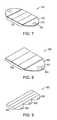
- FIGS. 7-11are perspective view of a two-source, one-source, asymmetric, two-source folded, and single-source folded light-guide elements, respectively, in accordance with embodiments of the invention.
- FIGS. 12-14depict various views of segment-assembly planar illumination areas in accordance with an embodiment of the invention.
- FIG. 15is a perspective view of a stripe planar-illumination unit in accordance with embodiments of the invention.
- FIGS. 16A and 16Bdepict perspective and plan views, respectively, of a planar illumination area assembled from the illumination unit shown in FIG. 15 ;
- FIGS. 17A and 17Bdepict perspective and plan views, respectively, of a planar illumination area assembled from asymmetric stripe elements in accordance with an embodiment of the invention
- FIG. 18is a plan view of a planar illumination area formed from folded two-source light-guide elements in accordance with an embodiment of the invention.
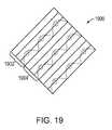
- FIG. 19is a perspective view of a planar illumination area formed from folded asymmetric light-guide elements in accordance with an embodiment of the invention.
- FIGS. 20-22depict cross-sections of non-uniform light emitted by a planar illumination area in accordance with embodiments of the invention.
- FIGS. 23 and 24are elevational views of light-guide element sidewall structures in accordance with embodiments of the invention.
- FIG. 25is a plan view of a planar illumination area with a transparent diffusive sheet in accordance with embodiments of the invention.
- FIG. 26is a perspective view of a back-light unit (BLU) application with tiled elements in accordance with an embodiment of the invention.
- BLUback-light unit
- FIG. 27is a perspective view of a planar illumination area covered by a light-absorbing surface in accordance with an embodiment of the invention.
- FIG. 28depicts a cross-section of a planar illumination area with a light-absorbing surface placed in the regions where light-guide elements overlap in accordance with an embodiment of the invention
- FIG. 29depicts a cross-section of two light-guide elements with transition regions in accordance with an embodiment of the invention.
- FIG. 30graphically depicts the power output of each element shown in FIG. 29 .
- FIGS. 31-36depict different methods and systems for overlapping light-guide elements to form planar illumination areas with transition regions, and the light-guide elements used therein, in accordance with embodiments of the invention
- FIGS. 37 and 38depict cross-sections of planar illumination areas made with light-guide elements having non-vertical sidewalls in their overlapping regions in accordance with embodiments of the invention
- FIG. 39Ais an elevation of one embodiment of a planar illumination area including a transparent filling material in accordance with an embodiment of the invention.
- FIG. 39Bis a perspective view of another embodiment of a planar illumination area including a transparent filling material in accordance with an embodiment of the invention.
- FIG. 40depicts an LED sub-assembly in accordance with an embodiment of the invention.
- FIGS. 41-43depict a carrier platform and bare-die LEDs, a printed circuit board, and an interface plate in accordance with embodiments of the invention
- FIG. 44depicts a bottom view of the LED sub-assembly
- FIG. 45is a perspective view of a planar illumination unit in accordance with embodiments of the invention.
- Described hereinare various embodiments of methods and systems for assembling a planar illumination area based on one or more discrete planar illumination units, various embodiments of different types of light-guide elements and LED sub-assemblies, and various embodiments of methods and systems for eliminating non-uniform “stitching” effects between planar illumination unit tiles.
- FIG. 2generically illustrates a monolithic structure 200 with an integrated upward-emitting light source 202 embedded fully within a light guide 208 .
- the light source 202may have a Lambertian light distribution, and light 204 is substantially retained within the light guide 208 for emission through a surface 210 thereof.
- the present inventionutilizes modular light-guide elements in which the light source is at least partially (and typically fully) embedded, facilitating the light retention and emission behavior shown in FIG. 2 .
- the elementsare tilable to facilitate uniformly illuminating surfaces of arbitrary size.
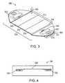
- a representative planar, tilable illumination unit 300is illustrated in perspective in FIG. 3 and sectionally in FIG. 4 .
- the illustrated planar illumination unit 300includes a pair of opposed LED sub-assembly modules 302 and a light-guide element 304 .
- the light-guide element 304may include various regions—e.g., an in-coupling region 306 , a concentration region 308 , a propagation region 310 , and an out-coupling region 312 —that optimize capture, retention, and emission of light.
- Each LED sub-assembly module 302desirably includes an LED light source at least partially packaged within the in-coupling region 306 of the light guide 304 , as further described below.
- Lightmay be emitted upward from the LED sources, which may be Lambertian sources, into the in-coupling region 306 of the light guide 304 , in which case the light propagates in lateral directions (i.e., is confined within the thickness of the light guide 304 ).
- the in-coupling and concentration regions 306 , 308 of the light-guide element 304in effect gather the light from the light source and direct it, with minimal losses, toward the propagation region 310 .
- the concentration region 308orients toward the out-coupling region 312 a substantial fraction of multidirectional light received in the in-coupling region 306 .
- the lightis emitted from the light guide, resulting in planar illumination with desired properties that depend on a particular application.
- substantially uniform illumination over the entire area of the out-coupling regionmay be preferred for back-lighting applications.
- substantially uniformis meant no more than 10% variation in output intensity.
- planar illumination systemsExemplary properties exhibited by planar illumination systems according to embodiments of the present invention are shown in FIG. 5 .
- the planar illumination system whose behavior is illustrated in FIG. 5includes, as discrete light sources, two RGB midsize LED chips, and the thickness of the system is approximately 5 mm. These planar illumination systems exhibit a brightness of approximately 2060 candelas per square meter (nits) with a brightness non-uniformity of only approximately ⁇ 6%.
- the color uniformity ( ⁇ x, ⁇ y)may be approximately ( ⁇ 0.008, ⁇ 0.006).
- the depicted cylindrical shape of the in-coupling region 306is for illustrative purposes only, and other shapes may be used.
- the in-coupling region 306may include two regions having annular or cylindrical profiles.
- One or more light sourcesfor example, white, single color, red-green-blue (RGB), or infrared (IR) light sources, as well as either bare-die or packaged LEDs, may be mounted at the back of the in-coupling region 306 . These light sources emit light that is coupled into the light guide through the in-coupling region 306 , which alters the direction of the light emitted by the LEDs to couple the light into the light-guide element 304 .
- the lightmay be emitted in all directions along the periphery of the in-coupling region 306 .
- In-couplingis described in U.S. application Ser. No. 12/155,090, titled “Method and Device for Providing Circumferential Illumination,” filed on Apr. 29, 2008, which is hereby incorporated by reference in its entirety.
- the in-coupling region 306may take the form of an optical funnel. The funnel receives light from one or more light-emitting elements and transmits the light into the propagation region 310 .
- the funnelmay take the form of a surface-emitting waveguide or a surface-emitting optical cavity that receives the light generated by one or more LEDs through an entry surface, distributes it within an internal volume, and emits it through an exit surface.
- the in-coupling region 306 and/or concentration region 308may include one or more reflectors (e.g., edge reflectors).
- the out-coupling region 312may be located on only one side of the in-coupling region 306 , the light that is emitted from the in-coupling region 306 on a side 316 opposite the out-coupling region 312 may be redirected toward the out-coupling region 312 .
- This redirectionmay occur in the concentration region 308 , where a concentrator may direct the light toward the out-coupling region 312 , as described in greater detail below.
- there is a concentrator for each LEDsuch as, for example, two LEDs and two concentrators.
- FIG. 3one embodiment of a parabola-shaped concentration region 308 is shown, but other shapes may be used.
- the center of the parabola formed by the concentration region 308may be the center of the in-coupling region 306 .
- the propagation region 310allows the light transmitted from the in-coupling region 306 and concentration region 308 to propagate freely toward the out-coupling region 312 .
- the lightis turned in an upward direction (as indicated at 318 ) from the planar illumination unit 300 to the outside world. This light may then illuminate a planar segment of a larger illumination surface formed by multiple tiled illumination units 300 such as, for example, a surface in an LCD backlight application.
- the out-coupling region 312is depicted as square-shaped in FIG. 3 , but, for illustrative purposes, is shown as three rectangular sub-regions 320 , 322 , 324 .
- These sub-regions 320 , 322 , 324are not separate regions, but instead show, in one embodiment, a representative distribution of dispersed particles within the out-coupling region 312 .
- These particlesfacilitate emission of the light by serving as scatterers, typically scattering optical radiation in more than one direction. When light is scattered by a particle such that the impinging angle is below the critical angle, no total internal reflection occurs and the scattered light is emitted through the surface of out-coupling region 312 along the direction 318 .
- the light-scattering particlesmay be beads, e.g., glass beads, or other ceramic particles, rubber particles, silica particles, particles including or consisting essentially of inorganic materials such as BaSO 4 or TiO 2 , particles including or consisting essentially of a phosphor material (as further described below), and the like.
- the light-scattering particlesare substantially or even completely non-phosphorescent. Such non-phosphorescent particles merely scatter light without converting the wavelength of any of the light striking the particles.
- the term “light-scattering particles”may also refer to non-solid objects embedded in the waveguide material from which core structure are made, provided that such objects are capable of scattering the light.
- suitable non-solid objectsinclude, without limitation, closed voids within the core structures, e.g., air bubbles, and/or droplets of liquid embedded within the core structures.
- the light-scattering particlesmay also be organic or biological particles, such as, but not limited to, liposomes.
- optical elementssuch as microlenses are utilized in conjunction with, or even instead of, light-scattering particles.
- the particlesare concentrated toward the center sub-region 322 of the out-coupling region 312 —i.e., the particle concentration in the center sub-region 322 exceeds the concentration in the peripheral sub-regions 320 , 324 , but typically the particle-concentration transition among sub-regions is gradual rather than abrupt.
- the same scattering materialmay be used for each region 306 , 308 , 310 , 312 but at different concentrations appropriate to the functions of the different regions.
- the out-coupling region 312typically contains the greatest concentration of particles.
- the concentration region 308may contain particles graded in concentration to direct light to the propagation region 310 , which typically contains no particles.
- the concentration region 308transfers the light that is coupled into the light-guide element 304 so that it propagates toward the propagation region 310 .
- the concentration region 308may enable the light from the in-coupling region 306 to the out-coupling region 312 to achieve the required distribution of light intensity.
- the in-coupling 306 , concentration 308 , and propagation 310 regionsmay be designed to evenly distribute light at the entrance 314 to the out-coupling region 312 .
- a standard structure for emitting light from the out-coupling region 312may enforce a uniform distribution of intensity at the entrance 314 to the out-coupling region 312 .
- FIG. 6illustrates an exemplary portion of a light-guide element 600 including a concentration region 602 , an in-coupling region 604 , and a propagation region 606 that increases the amount and uniformity of light intensity at the interface 610 to the out-coupling region by advancing the light toward the out-coupling region in a uniform manner.
- a side 608 of the light-guide element in the concentration region 602has a parabolic shape and/or a reflective coating.
- the center of the parabola formed by the concentration region 602may be the center of the in-coupling region 604 .
- Light that enters the light-guide element 600 at the in-coupling region 604may spread in all directions in the light-guide element 600 .
- the angular spreadis largely confined to the concentration region 602 and directed toward the propagation region 606 due to total internal reflection at the sidewall 608 .
- the critical anglemay be, for example, 41.8 degrees, such that any injected light propagating toward the sidewall 608 at or below this angle will ultimately reach the entrance 610 of the propagation region 606 , via a single or multiple reflections from the sidewall.
- the light intensitywill be a superposition of the light directly propagating to the propagation region 606 from the in-coupling region 604 and the light reflected from the sidewall 608 .
- the light intensity at the entrance 610 of the propagation region 606is substantially uniform. In this way, the light may propagate through the propagation region 606 and reach the entrance to the out-coupling region with a uniform intensity distribution.
- the light-guide element 304may be made using a waveguide material having a refractive index greater than one.
- materials suitable for the light-guide elementinclude 304 , without limitation, TPU (aliphatic), which has a refractive index of about 1.50; TPU (aromatic), which has a refractive index of from about 1.58 to about 1.60; amorphous nylon such as the GRILAMID material supplied by EMS Grivory (e.g., GRILAMID TR90), which has a refractive index of about 1.54; the TPX (PMP) material supplied by Mitsui, which has a refractive index of about 1.46; PVDF, which has a refractive index of about 1.34; other thermoplastic fluorocarbon polymers; the STYROLUX (UV stabilized) material marketed by BASF, which has a refractive index of about 1.58; polymethyl methacrylate (PMMA) with a refractive index of about
- TPUaliphatic
- TPU
- the light-guide element 304may consist of a single (core) layer or have a sandwich structure in which a core layer lies between opposed cladding layers.
- the thickness of the cladding layersis typically from about 10 ⁇ m to about 100 ⁇ m.
- the thickness of the core layermay vary from approximately 400 ⁇ m to approximately 1300 ⁇ m.
- the material from which the light-guide elements 304 are formedis transparent, is at least somewhat flexible, possesses at least some elongation capability, and/or is capable of being produced in a thermoplastic process.
- Very flexible materialssuch as silicone may be suitable, as well as less flexible materials such as PMMA or polycarbonate.
- the degree to which the chosen material is capable of bendingmay depend on the mode of assembling sets of elements into a surface. For example, some assembly procedures may require little or no bending. In other embodiments, the material is not inherently flexible; even a relatively stiff material, if thin enough, may exhibit sufficient mechanical flexibility to accommodate assembly as described herein.
- the waveguide elementsmay be manufactured by any suitable technique including, without limitation, co-extrusion, die cutting, co-injection molding, or melting together side-by-side in order to introduce bends that will facilitate assembly.
- Each region 306 , 308 , 310 , 312 of the light-guide element 304may include phosphorescent materials that change the wavelength of the light striking them to another wavelength, thereby, for example, altering the color of the light. In this manner, white light may be produced by altering the wavelength of some of the light emitted from the light sources.
- portions of the lightmay be absorbed by the phosphorescent material, which then emits light of a different wavelength. Light with different wavelengths may be collectively emitted by the out-coupling region, forming white light.
- FIG. 7illustrates one embodiment of a two-source light-guide element 700 in accordance with the present invention.
- the two-source light-guide element 700has an in-coupling region 702 , a concentration region 704 , a propagation region 706 , and an out-coupling region 708 .
- the out-coupling region 708may be square-shaped, as shown, thereby allowing a first light-guide element 700 to be tiled next to a second, similar light-guide element 700 rotated by 90 degrees.
- the out-coupling region 708 of the first light-guide element 700may be positioned above the in-coupling region 702 , concentration region 704 , and propagation region 706 of the second light-guide element 700 , thereby hiding those regions of the second light-guide element; the result of tiling in this fashion is to produce a uniform illumination surface without dark regions.
- the out-coupling region 708is rectangular.
- FIG. 8illustrates, in another embodiment, a single-source light-guide element 800 that has only a single in-coupling region 802 for receiving light from a single source.
- the single-source light-guide element 800also includes a concentration region 804 , a propagation region 806 , and an out-coupling region 808 .
- Lightpropagates from the in-coupling region 802 to the out-coupling region 808 in a single direction.
- assembly of a planar illumination area using single-source light-guide elements 800does not require them to be bent (since they may be tiled in a manner that allows the out-coupling region 808 to occlude the concentration region 806 of an adjacent element).
- the number of discrete light-guide element 800 needed for assembly of the tiled planar illumination areaincreases with the square of the increase in the surface diagonal of the illumination surface.
- the out-coupling region 808is, in various embodiments, rectangular or square-shaped.
- Light-guide elements in accordance with the inventionmay have multiple light sources arranged in a single side of the element, as illustrated in FIG. 9 .
- the depicted asymmetric light-guide element 900has the form of a stripe with a single out-coupling region 902 and a plurality of adjacent in-coupling 904 , propagation 906 , and concentration regions 908 .
- the in-coupling regionsare disposed on only one side of the out-coupling region 902 , and light therefore reaches the out-coupling region 902 from only one side rather than from two.
- the asymmetric light-guide element 900may be used to assemble a planar illumination area of any size.
- the out-coupling region 902is typically rectangular, as illustrated, but may be square or any other shape.
- FIG. 10shows, in one embodiment, a folded two-source two-direction light-guide element 1000 .
- the folded element 1000has the configuration of two-source light-guide element 700 , but is folded over on itself such that the two light sources, in-coupling region 1002 , concentration region 1004 , and propagation region 1006 are hidden under the light-guide element's out-coupling region 1008 .
- the folded two-source light-guide element 1000may have a square-shaped out-coupling region 1008 ; the symmetry of the square shape is desirable in allowing the folded two-source light-guide elements 1000 to be tiled side-by-side.
- each folded two-source light-guide element 1000is rotated 90 degrees with respect to a neighboring element 1000 so that each folded side of one element 1000 abuts an unfolded side of a neighboring element 1000 .
- the number of square two-source light-guide elements 1000 needed for a planar illumination area assemblyincreases with the square of the increase in the area diagonal.
- FIG. 11shows a folded single-source, two-direction light-guide element 1100 .
- This light-guide elementis similar to the folded two-source light-guide element 1000 , except that only one light source is present, and the in-coupling regions 1102 overlap.
- Lightpropagates from the light source to the out-coupling region 1104 from opposite directions, i.e., through the in-coupling regions 1102 .
- the number of square one-source light-guide elements 1100 needed for the planar illumination area assemblyincreases with the square of the increase in the area diagonal.
- the two-source light-guide element 700 , single-source light-guide element 800 , asymmetric light-guide element 900 , folded two-source light-guide element 1000 , and/or folded one-source light-guide element 1100may be modified to change their properties in accordance with functional requirements.
- the manner in which the in-coupling, concentration, and propagation regions mate with the out-coupling regionmay be modified.
- light from a single sourceis coupled to an out-coupling region from two or more directions, thereby enabling more efficient and uniform out-coupling of the light.
- Other modificationsmay be made as well, such as changing the shape of the out-coupling region to be either square or rectangular.
- a square shapeimparts rotational symmetry, which may simplify assembly of the planar illumination, while a rectangular shape facilitates assembly of a rectangular planar illumination of any desired size.
- the flexibility of a light-guide elementmay be adjusted to comply with a particular tiling or folding technique, which may require that a light-guide element be bent to hide a non-illuminated area of an adjacent light-guide element.
- a light-guide elementmay also have more than one light source.
- the size of the light-guide elementmay be adjusted to change the total number of light-guide elements required to assemble a planar illumination area; for example, a single planar configuration may utilize elements having different sizes or configurations.
- an area of a light-guide element that does not emit lightmay be occluded by (i.e., hidden behind) an area of another light-guide element that does emit light; in particular, in-coupling, concentration, and/or propagation regions may be hidden under an out-coupling region.
- the out-coupling regionmay be coupled to an in-coupling region on a different light-guide element. Accordingly, a large, uniformly illuminated surface may be built even though some areas of the light-guide element used to create the surface do not emit light.
- the surfacemay be configured in a variety of shapes, including curved shapes or spheres.
- the planar illumination areamay be used to provide substantially uniform illumination in a variety of applications.
- the planar illumination areais used as a luminaire for lighting applications.
- the planar illumination areais used as a backlight unit for a display device, e.g., a liquid crystal display (LCD).
- the LCDincludes a plurality of pixels and is placed in front of the light-guide elements.
- Each planar illumination unitmay represent an independent unit that produces and/or transfers light.
- a planar illumination areamay be assembled from planar illumination units according to any of various suitable assembly techniques, such as segment assembly, stripe assembly, tile assembly, or folded architecture assembly, each described in more detail below.
- Segment assemblyis a technique wherein, for the light-guide elements described above, each light-guide element is simply placed face-up on a surface.
- the out-coupling regions of some light-guide elementsare arranged to cover the in-coupling regions of other light-guide elements previously put in place.
- the out-coupling regions of previously placed light-guide elementsare lifted so that the in-coupling regions of new light-guide elements can be slipped underneath. This lifting step may require that at least some of the light-guide elements exhibit sufficient flexibility to facilitate lifting.
- each light-guide elementhas a rectangular out-coupling region that hides zero, one, or two light sources.
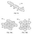
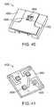
- FIG. 12illustrates an example of the segment assembly technique wherein a planar illumination area 1200 is constructed from nine discrete light-guide elements 1202 , which correspond to element 700 (but may be, in various embodiments, any of the light-guide elements described above).
- the structure 1200emits light only from the square or rectangular out-coupling regions 1204 of the light-guide elements 1202 .
- the in-coupling, concentration, and propagation regions 1206 , 1208 , and 1210 of the light-guide elements 1202do not emit light.
- FIG. 13illustrates a portion 1300 of the planar illumination area 1200 in greater detail.
- An in-coupling region 1206 of first light-guide element 1202is hidden under a light-emitting out-coupling region 1204 ′ of a second light-guide element 1202 ′.
- the out-coupling region 1204 ′′ of an adjacent elementreceives light from another in-coupling region 1206 ′ of element 1202 ′.
- FIG. 14illustrates another segment assembly technique for constructing a large planar illumination area from discrete light-guide elements 1402 .
- nine light-guide element 1402are assembled in the manner shown into a three-by-three grid 1405 such that the non-light-emitting portions of each light-guide element 1402 are hidden behind light-emitting portions of an adjacent light-guide element 1402 .
- the integration principle illustrated in FIG. 14may be applied to planar illumination areas of arbitrary size, shape, and grid number.
- the symmetric stripe element 500represents a daisy-chaining of light-guide elements 1502 such that each light-guide element 1502 shares a light source with a neighboring light-guide element 1502 .
- in-coupling regions 1504 of neighboring light-guide elements 1504overlap, and a stripe of N light-guide elements requires only N+1 light sources.
- Each out-coupling region 1506receives light from two directions propagated from in-coupling regions 1504 .
- the out-coupling region 1506may be square or rectangular.
- the light-guide elements 1502may need to be bent to assemble a planar illumination area with stripes 1500 .
- the number of discrete light-guide elements needed for the planar illumination area assemblymay increase linearly with an increase in the area diagonal.
- a planar illumination area 1600may be assembled from stripes 1500 by arranging a first set of stripes 1500 adjacently, and then weaving a second set of adjacent stripes perpendicularly through the first set of stripes.
- the over-and-under weavingis carried out so as to place an out-coupling region 1506 over each in-coupling region 1504 and its associated concentration and propagation regions.
- This proceduregenerally requires that the light-guide elements 1502 exhibit some flexibility to permit interweaving to take place.
- FIGS. 17A and 17Bshow an exemplary planar illumination area 1700 assembled using asymmetric light-guide elements 1702 , which correspond to the elements 900 shown in FIG. 9 .
- a first asymmetric light-guide element 1702is placed at the end edge of the illumination area.
- a second asymmetric light-guide element 1704is placed next to the first asymmetric light-guide element 1702 such that the out-coupling region 1706 of the second asymmetric light-guide element 1704 covers the in-coupling regions 1708 of the asymmetric light-guide element 1702 .
- Other asymmetric light-guide elementsare added in the same fashion. This assembly technique does not require element flexibility because each tile may be pre-formed to a desired form factor, and thus the asymmetric light-guide elements 1702 need not be bent.
- single-source light-guide elements(corresponding to the elements 800 shown in FIG. 8 ) are placed adjacent to each other to form a group of elements similar to an asymmetric light-guide element 1702 , and then this group of elements is used to form a structure corresponding to the planar illumination area 1700 .
- FIG. 18shows how a planar illumination area 1800 may be formed from folded two-source light-guide elements 1802 (corresponding to the elements 1000 shown in FIG. 10 ), which are simply tiled adjacently.
- the planar illumination area 1800may also formed from folded one-source light-guide elements (corresponding to the elements 1100 shown in FIG. 11 ).
- the folded light-guide elements 1802do not require hiding one light-guide element behind another adjacent light-guide element because the out-coupling region of each folded light-guide element hides the in-coupling region of that light-guide element.
- FIG. 19shows a planar illumination area 1900 assembled using a multiple-light-source light-guide element 1902 (similar to the multiple-light-source element 900 shown in FIG. 9 ) that has its in-coupling, concentration, and propagation regions folded underneath its out-coupling region. Because the out-coupling region of one folded multiple-light-source light-guide element 1902 need not be used to hide the in-coupling, concentration, and propagation regions of an adjacent folded multiple-light-source light-guide element 1904 , the element 1902 can simply be tiled adjacently; it is not necessary to bend the elements 1902 to achieve planar assembly.
- a planar illumination area assembled from a plurality of light-guide elements as discussed abovemay emit non-uniform light at the boundary regions, or “stitches,” between tiles.
- the non-uniform lightmay be due to the configuration of the light-guide elements, stray light in the system, and/or roughness or roundness in a sidewall of a light-guide element owing to, for example, the light-guide elements themselves or their method of assembly.
- the structure of a planar illumination area that places each light-guide element perpendicular to an adjacent light-guide elementmay create a problem of uniformity in the borders of the light-guide elements due to the positioning of the axis of the progress of the light between the adjacent tiles.
- the direction of the light emission from the tile in the out-coupling regionmay be similar to the direction of the progress of the light in the light-guide.
- FIG. 20illustrates a cross-section of a planar illumination area 2000 in which one light-guide element 2002 is laid on the surface of an adjacent light-guide element 2004 .
- This configurationmay allow stray light 2010 to pass from an in-coupling region 2008 of the first light-guide element, between the two light-guide elements 2002 , 2004 , and then to emerge on the outside 2010 of the planar illumination area 2000 .
- light 2102 emitted from a lower light-guide element 2104 close to the edge of an upper light-guide element 2106may meet and be reflected from a sidewall 2108 of the upper light-guide element 2106 .
- the original trajectory 2110 of the light 2102may thus be changed to the reflected path 2112 .
- the sidewall 2108 of the upper light-guide element 2106may create a non-uniform light pattern near it because it reflects emitted light 2102 away from it.
- Non-uniform lightmay also arise due to roughness and/or roundness of the sidewall of a light-guide element.
- FIG. 22illustrates a structure 2200 in which two adjacent light-guide elements 2202 , 2204 are separated by a distance d because of, for example, imperfections in the sidewalls 2206 of the light-guide elements 2202 , 2204 .
- the gap 2208 between the light-guide elements 2202 , 2204may also create a gap in the distribution of emitted light 2210 .
- the amount of non-uniform light emitted at the borders of the light-guide elementsmay be reduced.
- a structuremay be added to a planar illumination area that creates blurring and conceals the visibility of the borders between the light-guide elements.
- the walls of a light-guide elementare modified to reduce the light emitted therefrom, and thereby reduce the non-uniform light emitted at the borders between light-guide elements.
- the walls of the light-guide elementmay be covered in a material that absorbs or reflects light, but does not prevent the emission of intensified light from the end area. This diffuses at least part of the light hitting the sidewall of the light-guide element in many directions, and the light is emitted from the upper or lower surface of the light-guide.
- the wall of the light-guide elementis polished to a tolerance of approximately 20 nm root-mean-square or 150 nm peak-to-peak so that the light incident on the sidewall of the light-guide element may be reflected or refracted instead of diffused. In another embodiment, the wall of the light-guide element is polished to a tolerance less than approximately 600 nm peak-to-peak. If the light is refracted, it may pass through the propagating light-guide element and enter a neighboring light-guide element, where it may be emitted or again refracted. If the light is reflected, it may continue to propagate in the original light-guide element.
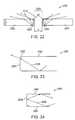
- FIG. 23shows a portion of a light-guide element 2300 wherein the junction 2302 , where the sidewall 2304 of the light-guide element meets a surface 2306 of the light-guide element 2300 , is curved.
- the curved area 2304changes the angle of incidence of the light 2308 striking it, thereby permitting the light 2308 to be refracted out of the light-guide element 2300 .
- lightmay also be emitted from a polished sidewall of a light-guide element if the light striking a portion of the sidewall strikes with an appropriate angle in relation to the critical incident angle.
- the sidewall 2402 of the light-guide element 2400creates a right angle with respect to the upper and lower surfaces 2404 , 2406 of the light-guide element 2400 .
- the angle of the sidewall 2402 of the light-guide element 2400alone or in combination with the polishing of the sidewall 2402 , causes light 2408 reaching the sidewall 2402 to be reflected, rather than being emitted from the light-guide element 2400 .
- a diffusive sheetmay be used to reduce non-uniform light emitted from the borders of a light-guide element. Light is thereby emitted at a wide angle from the surface of a light-guide element near the border and in a transverse direction compared to the direction of the border line. Coupling two light-guide elements that emit in this manner blurs the visibility of the border line with the help of a transparent diffusive sheet having a small diffusion value, such as, for example, 10-20% diffusive direction transmission and 80-70% reserve direction transmission.
- a planar illumination area 2500may be covered by a transparent diffusive sheet.
- each light-guide element 2502is sized 82 mm by 63 mm, and is separated from a neighboring light-guide element by 6 mm.
- the distance of the highest diffuser from the illuminated surfaceis 4.5 mm.
- the non-uniformity of the stitch at the center of the black rectangle of FIG. 26may be simulated using the calculation:
- Non - Uniformity ⁇ [ % ]⁇ Max - Min Max + Min , which, when applied to the planar illumination area 2500 , indicates that the non-uniformity in light emission without using a diffuser is ⁇ 22%, while the non-uniformity with a diffuser in place is ⁇ 7%.
- Emission of light at a wide anglemay enable blurring of the border lines between light-guide elements joined together along one axis and laid over one another along a perpendicular axis.
- Lightmay be emitted a wide angle in a direction perpendicular to the border line between light-guide elements, and at a narrow angle in a direction parallel to the border line, and a diffuser sheet may be placed over the light-guide elements.
- This structureincreases the brightness of the illuminating surface, which may be useful for, for example, backlight unit (BLU) applications in which a brightness enhancement film (“BEF”) sheet is used to reduce the angle of the emitted light and obtain greater brightness.
- BLUbacklight unit
- BEFbrightness enhancement film
- a BLU 2200includes light-guide elements 2602 tiled next to one another in the direction of the horizontal axis 2604 and laid on top of one another in the direction of the vertical axis 2606 .
- the propagation direction of light in a light-guide element 2602is continuous with respect to another aligned light-guide element, and mixing in the propagation direction of the light is thereby reduced.
- the mixing of the light directionsmay be balanced by a suitable arrangement of optical prism sheets 2702 , such as BEF sheets, that are placed above a planar illumination area 2704 to form a composite structure 2700 .
- the direction of the optical prism sheets 2702is generally aligned in the propagation direction of the light in the light-guide elements 2706 , and each optical prism sheet 2702 overlies the out-coupling region 2708 of a light-guide element 2706 , separated by a gap 2710 .
- a light-absorbing surface 2802may be placed in the region 2804 where two light-guide elements 2806 , 2808 overlap to reduce the amount of light escaping between them, as explained with reference to FIG. 20 .
- the light-absorbing surface 2802may be a prism optical foil, such as a BEF sheet, that reduces the exit angles of this light, or, alternatively, bends the light back into the light-guide elements 2806 , 2808 by allowing it to be coupled and spread inside. The light may thus be recycled so that it joins the light spreading in the light-guide elements 2806 , 2808 .
- the stray lightis at an obtuse angle relative to the perpendicular direction of the light-guide elements 2806 , 2808 , more of the light may be recovered by the light-absorbing element 2802 .
- Adjacent light-guide elementsmay be overlapped to reduce a sharp contrast between the illumination of the light-guide elements.
- FIG. 29shows a structure 2900 in which a first light-guide element 2902 is laid on top of an adjacent light-guide element 2904 .
- the area of light emission of the upper light-guide element 2902covers not only the in-coupling, concentration, and propagation regions of the lower light-guide element 2904 , but also a portion of its out-coupling region. This configuration allows the creation of a transition or overlap region 2906 between the light-guide elements 2902 , 2904 .
- an edge 2908 of the upper light-guide element 2902forms a non-straight line.
- Lightis transmitted from the out-coupling area of the lower light-guide element 2904 through the upper light-guide element 2902 to create a gradual change in the strength of the light across the transition area 2906 between the light-guide elements 2902 , 2904 .
- This gradual changemay be created by gradually decreasing the density of light-scattering elements (e.g., particles as described above) 2910 within each of the light-guide elements 2902 , 2904 in the transition region 2906 .
- FIG. 30illustrates how the output power of each of the light-guide elements 2902 , 2904 gradually decreases within the transition zone 2906 .
- the sum 3000 of the output power of both light-guide elements 2902 , 2904should be approximately constant (i.e., uniform) across the area of the transition zone 2906 .
- the output power between the transition region 2906 and the non-overlapping out-coupling regions of the light-guide elements 2902 , 2904is substantially uniform, i.e., differs by no more than 10%.
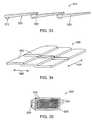
- FIG. 31Another planar illumination area 3100 made from overlapping light-guide elements 3102 is shown in FIG. 31 .
- the light-guide elements 3102are tiled in a graded manner in one direction 3104 and placed tightly together in the other direction 3106 .
- FIGS. 32A and 32Bshow a top and bottom views 3200 , 3202 , respectively, of a light-guide element 3204 that may be used in the structure 3100
- FIG. 33shows a side view 3300 .
- Transition regions 3206exist on both sides of an out-coupling region 3208 .
- Each light-guide element 3204also features a bottom reflector 3210 , a light source 3212 , and a transparent region 3214 . In this configuration, where the out-coupling region of an element underlies the out-coupling region of another element, it is transparent so as not to augment the light emitted from the overlying out-coupling region.
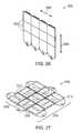
- a planar illumination area 3400may be constructed by overlapping a series of light-guide elements 3402 in two directions 3404 , 3406 .
- a transition region 3502surrounds the out-coupling region 3504 on all four sides thereof, as shown by the top view 3500 and bottom view 3600 of a light-guide element 3508 , allowing four other tiles to overlap, or be overlapped by, all four sides of the transition region 3502 .
- An out-coupling region 3504 , light source 3506 , bottom reflector 3602 , and transparent region 3604are also shown.
- the transition region 3502may be transparent on two or four sides, for example, depending on the characteristics of the transition regions of adjacent tiles; the objective, once again, is to retain a constant light output across the overlapping regions.
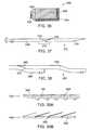
- a sidewall of a first light-guide elementmay be formed such that overlapping the first light-guide element with a second does not cause a lack of uniformity in the height of the formed planar illumination area.
- a first sidewall 3702 of a first light-guide element 3704may be non-vertical
- a second sidewall 3706 of an adjacent, second light-guide element 3708may be non-vertical and complementary to the first sidewall 3706 .
- the two light-guide elements 3704 , 3708overlap in a region 3710 that includes the non-vertical sidewalls 3702 , 3706 without a variation in the height h of the planar illumination area 3700 .
- a sidewall 3802 of a first light-guide element 3804may be curved to fit into the curvature 3806 of an adjacent, second light-guide element 3808 .
- FIGS. 39A-Billustrate, in alternative embodiments, side views of two planar illumination areas 3900 , 3902 that include a transparent filling material 3904 .
- the planar illumination area 3900uses the transparent filling material 3904 to reduce irregularities in the height of the area 3900 produced by overlapping light-guide elements 3906 .
- the refractive index of the transparent filling material 3904preferably matches the refractive index of the light-guide elements 3906 .
- use of the transparent filling material 3904creates a flat and smooth illumination surface 3908 .
- the planar illumination area 3902includes transparent filling material 3904 in the space between the light-guide elements 3906 , and this transparent filling material 3904 preferably has a refractive index that matches the refractive index of the light-guide elements 3906 .
- Utilization of a tile structure with a polished wall, as described above, in connection with the planar illumination area 3902may help create continuity between each light-guide element and its neighbor, allowing the light to spread between neighboring tiles.
- the merging of the light between the neighboring tilesdesirably creates continuous and monotonic change in the intensity of the light between the two sides of the stitch line without the need for an overlapping structure as described above.
- an LED sub-assemblyis attached to a light-guide element.
- the LED sub-assemblyfunctions as a platform for at least one light source and provides electrical and mechanical connectivity to the light-guide element.
- FIG. 40illustrates an exemplary embodiment of an LED sub-assembly 4000 , including a carrier platform 4002 , LED bare-die chips 4004 , a printed circuit board (“PCB”) 4006 , and an interface plate 4008 . These components are shown in greater detail in FIGS. 41-44 .
- the LED bare-die chips 4004may be replaced with packaged LED, RGB, or white light sources.
- the light sourcesmay be either side-emitting or top-emitting (i.e., Lambertian) sources.
- FIG. 41illustrates a structure 4100 including a carrier platform 4002 suitable for supporting one or more light sources.
- the light sourcesmay be, for example, bare-die LED chips 4004 .
- the carrier platform 4002may be any platform used for the assembly of LEDs, and, in one embodiment, exhibits good thermal conductivity.
- the carrier platform 4002may mechanically support the LED bare-die chips 4004 , enable heat dissipation from the LED bare-die chips 4004 by thermal conduction, and provide electrical connectivity to the LED bare-die chips 4004 .
- FIGS. 42A and 42Billustrate, in one embodiment, top and bottom views, respectively, of the printed circuit board 4006 .
- the carrier platform 4002 with the LED bare-die chips 4004may be mounted on the printed circuit board 4006 via a connector.
- the printed circuit board 4006includes a contour electrical interface to supply electrical current to the light sources.
- the printed circuit board 4006also mechanically supports the carrier platform 4002 and is in thermal contact therewith, thus enhancing heat dissipation from the light sources.
- FIG. 43illustrates one embodiment of the interface plate 4008 , which provides mechanical connectivity and support to an illumination source.
- the interface platemechanically connects the entire LED sub-assembly 4000 to a light-guide element. Further, it may enable mechanical connection of a planar illumination source to the required application structure. It may also assist thermal dissipation by providing thermal connectivity between the planar illumination source and the application structure.
- FIG. 44illustrates a bottom view of the LED sub-assembly 4000 , in which an electrical interface 4402 , mechanical interface 4404 , and heat conduction interface 4406 are visible.
- FIG. 45shows the LED sub-assembly 4000 assembled together with a light-guide element 4502 to form a planar illumination source 4500 .
- the LED bare-die chip 4004mounted on the carrier platform 4002 , may be placed in a suitable socket formed by the joining of the LED sub-assembly 4000 and the in-coupling region 4504 of the light-guide element 4502 .
- the light emitted from a LED bare-die chip 4004is coupled to the in-coupling region 4504 of the light-guide element 4502 .
- the LED bare-die chip 4004is placed in the LED sub-assembly 4000 , which is then attached to the light-guide element 4502 following other assembly steps that require high temperatures (e.g., higher than approximately 85° C.) that may damage the polymers in the light-guide element. Any gaps between the in-coupling region 4504 of the light-guide element 4502 and the carrier platform 4002 may be filled with a suitable filler material.
- the filler materialcan tolerate the operating temperatures of the LED (e.g., lower than approximately 150° C., or even lower than approximately 70° C.), but may not be capable of tolerating the higher temperatures required for assembly (e.g., soldering, at approximately 250° C.) of the LED sub-assembly 4000 .
- the filler materialgenerally fills the LED socket and covers the surface of the LED die and any wire bonds connected thereto.
- suitable filler materialsinclude UV-curable adhesives such as LIGHT WELD 9620, available from Dymax Corporation of Torrington, Conn., and encapsulation gels such as LS-3249 and LS-3252, available from NuSil Technology LLC of Wareham, Mass.
- the LED bare-die chip 4004may be coupled directly into the light-guide element 4502 using an intermediary material with suitable optical and mechanical characteristics.
- This intermediary materialmay be all or a portion of an encapsulation structure disposed over the LED bare-die chip 4004 .
- the form of the encapsulationis dictated by the shape and refractive-index requirements of the optical interface with the light-guide element 4502 . If an encapsulation element is used, the space between the walls of the socket in the light-guide element 4502 and the external surface of the encapsulation structure may be filled with optical glue with suitable optical and mechanical characteristics.
Landscapes
- Physics & Mathematics (AREA)
- General Physics & Mathematics (AREA)
- Optics & Photonics (AREA)
- Engineering & Computer Science (AREA)
- Manufacturing & Machinery (AREA)
- Planar Illumination Modules (AREA)
Abstract
Description
which, when applied to the
Claims (21)
Priority Applications (1)
| Application Number | Priority Date | Filing Date | Title |
|---|---|---|---|
| US12/888,932US8064743B2 (en) | 2007-12-19 | 2010-09-23 | Discrete light guide-based planar illumination area |
Applications Claiming Priority (7)
| Application Number | Priority Date | Filing Date | Title |
|---|---|---|---|
| US611007P | 2007-12-19 | 2007-12-19 | |
| US6438408P | 2008-03-03 | 2008-03-03 | |
| US12709508P | 2008-05-09 | 2008-05-09 | |
| US5993208P | 2008-06-09 | 2008-06-09 | |
| US12/324,555US7907804B2 (en) | 2007-12-19 | 2008-11-26 | Elimination of stitch artifacts in a planar illumination area |
| US12/771,411US7826698B1 (en) | 2007-12-19 | 2010-04-30 | Elimination of stitch artifacts in a planar illumination area |
| US12/888,932US8064743B2 (en) | 2007-12-19 | 2010-09-23 | Discrete light guide-based planar illumination area |
Related Parent Applications (1)
| Application Number | Title | Priority Date | Filing Date |
|---|---|---|---|
| US12/771,411ContinuationUS7826698B1 (en) | 2007-12-19 | 2010-04-30 | Elimination of stitch artifacts in a planar illumination area |
Publications (2)
| Publication Number | Publication Date |
|---|---|
| US20110013415A1 US20110013415A1 (en) | 2011-01-20 |
| US8064743B2true US8064743B2 (en) | 2011-11-22 |
Family
ID=40788386
Family Applications (5)
| Application Number | Title | Priority Date | Filing Date |
|---|---|---|---|
| US12/324,555ActiveUS7907804B2 (en) | 2007-12-19 | 2008-11-26 | Elimination of stitch artifacts in a planar illumination area |
| US12/324,544Active2031-11-03US8550684B2 (en) | 2007-12-19 | 2008-11-26 | Waveguide-based packaging structures and methods for discrete lighting elements |
| US12/324,540Expired - Fee RelatedUS8172447B2 (en) | 2007-12-19 | 2008-11-26 | Discrete lighting elements and planar assembly thereof |
| US12/771,411ActiveUS7826698B1 (en) | 2007-12-19 | 2010-04-30 | Elimination of stitch artifacts in a planar illumination area |
| US12/888,932ActiveUS8064743B2 (en) | 2007-12-19 | 2010-09-23 | Discrete light guide-based planar illumination area |
Family Applications Before (4)
| Application Number | Title | Priority Date | Filing Date |
|---|---|---|---|
| US12/324,555ActiveUS7907804B2 (en) | 2007-12-19 | 2008-11-26 | Elimination of stitch artifacts in a planar illumination area |
| US12/324,544Active2031-11-03US8550684B2 (en) | 2007-12-19 | 2008-11-26 | Waveguide-based packaging structures and methods for discrete lighting elements |
| US12/324,540Expired - Fee RelatedUS8172447B2 (en) | 2007-12-19 | 2008-11-26 | Discrete lighting elements and planar assembly thereof |
| US12/771,411ActiveUS7826698B1 (en) | 2007-12-19 | 2010-04-30 | Elimination of stitch artifacts in a planar illumination area |
Country Status (2)
| Country | Link |
|---|---|
| US (5) | US7907804B2 (en) |
| JP (1) | JP2011508373A (en) |
Cited By (34)
| Publication number | Priority date | Publication date | Assignee | Title |
|---|---|---|---|---|
| US20090141476A1 (en)* | 2005-06-07 | 2009-06-04 | Noam Meir | Illumination Apparatus and Methods of Forming the Same |
| US20100296270A1 (en)* | 2008-01-25 | 2010-11-25 | Showa Denko K.K. | Display device and light emitting device |
| US20110080532A1 (en)* | 2009-10-02 | 2011-04-07 | Hitachi Consumer Electronics Co., Ltd. | Backlight unit and video display apparatus applying the same therein |
| US8172447B2 (en) | 2007-12-19 | 2012-05-08 | Oree, Inc. | Discrete lighting elements and planar assembly thereof |
| US8182128B2 (en) | 2007-12-19 | 2012-05-22 | Oree, Inc. | Planar white illumination apparatus |
| US20120155113A1 (en)* | 2005-06-07 | 2012-06-21 | Eran Fine | Illumination apparatus |
| US8231237B2 (en) | 2008-03-05 | 2012-07-31 | Oree, Inc. | Sub-assembly and methods for forming the same |
| US8272758B2 (en) | 2005-06-07 | 2012-09-25 | Oree, Inc. | Illumination apparatus and methods of forming the same |
| US8301002B2 (en) | 2008-07-10 | 2012-10-30 | Oree, Inc. | Slim waveguide coupling apparatus and method |
| US20130182455A1 (en)* | 2012-01-18 | 2013-07-18 | Electronics And Telecommunications Research Institute | Display device |
| US8591072B2 (en) | 2011-11-16 | 2013-11-26 | Oree, Inc. | Illumination apparatus confining light by total internal reflection and methods of forming the same |
| US8629475B2 (en) | 2012-01-24 | 2014-01-14 | Cooledge Lighting Inc. | Light-emitting dies incorporating wavelength-conversion materials and related methods |
| US8896010B2 (en) | 2012-01-24 | 2014-11-25 | Cooledge Lighting Inc. | Wafer-level flip chip device packages and related methods |
| US20140355302A1 (en)* | 2013-03-15 | 2014-12-04 | Cree, Inc. | Outdoor and/or Enclosed Structure LED Luminaire for General Illumination Applications, Such as Parking Lots and Structures |
| US8907362B2 (en) | 2012-01-24 | 2014-12-09 | Cooledge Lighting Inc. | Light-emitting dies incorporating wavelength-conversion materials and related methods |
| US9164218B2 (en) | 2008-07-10 | 2015-10-20 | Oree, Inc. | Slim waveguide coupling apparatus and method |
| US9291320B2 (en) | 2013-01-30 | 2016-03-22 | Cree, Inc. | Consolidated troffer |
| US9343443B2 (en) | 2014-02-05 | 2016-05-17 | Cooledge Lighting, Inc. | Light-emitting dies incorporating wavelength-conversion materials and related methods |
| US9366396B2 (en) | 2013-01-30 | 2016-06-14 | Cree, Inc. | Optical waveguide and lamp including same |
| US9366799B2 (en) | 2013-03-15 | 2016-06-14 | Cree, Inc. | Optical waveguide bodies and luminaires utilizing same |
| US9389367B2 (en) | 2013-01-30 | 2016-07-12 | Cree, Inc. | Optical waveguide and luminaire incorporating same |
| US9442243B2 (en) | 2013-01-30 | 2016-09-13 | Cree, Inc. | Waveguide bodies including redirection features and methods of producing same |
| US9625638B2 (en) | 2013-03-15 | 2017-04-18 | Cree, Inc. | Optical waveguide body |
| US9690029B2 (en) | 2013-01-30 | 2017-06-27 | Cree, Inc. | Optical waveguides and luminaires incorporating same |
| US9798072B2 (en) | 2013-03-15 | 2017-10-24 | Cree, Inc. | Optical element and method of forming an optical element |
| US9857519B2 (en) | 2012-07-03 | 2018-01-02 | Oree Advanced Illumination Solutions Ltd. | Planar remote phosphor illumination apparatus |
| US9869432B2 (en) | 2013-01-30 | 2018-01-16 | Cree, Inc. | Luminaires using waveguide bodies and optical elements |
| US9920901B2 (en) | 2013-03-15 | 2018-03-20 | Cree, Inc. | LED lensing arrangement |
| US10209429B2 (en) | 2013-03-15 | 2019-02-19 | Cree, Inc. | Luminaire with selectable luminous intensity pattern |
| US10416377B2 (en) | 2016-05-06 | 2019-09-17 | Cree, Inc. | Luminaire with controllable light emission |
| US10436970B2 (en) | 2013-03-15 | 2019-10-08 | Ideal Industries Lighting Llc | Shaped optical waveguide bodies |
| US10502899B2 (en)* | 2013-03-15 | 2019-12-10 | Ideal Industries Lighting Llc | Outdoor and/or enclosed structure LED luminaire |
| US11112083B2 (en) | 2013-03-15 | 2021-09-07 | Ideal Industries Lighting Llc | Optic member for an LED light fixture |
| US11719882B2 (en) | 2016-05-06 | 2023-08-08 | Ideal Industries Lighting Llc | Waveguide-based light sources with dynamic beam shaping |
Families Citing this family (47)
| Publication number | Priority date | Publication date | Assignee | Title |
|---|---|---|---|---|
| WO2004053531A2 (en)* | 2002-12-09 | 2004-06-24 | Oree, Advanced Illumination Solutions Inc. | Flexible optical device |
| KR101548025B1 (en)* | 2007-07-27 | 2015-08-27 | 아사히 가라스 가부시키가이샤 | Translucent substrate, method for manufacturing the translucent substrate, organic led element and method for manufacturing the organic led element |
| US8462292B2 (en)* | 2008-07-31 | 2013-06-11 | Rambus Delaware Llc | Optically transmissive substrates and light emitting assemblies and methods of making same, and methods of displaying images using the optically transmissive substrates and light emitting assemblies |
| US8223296B2 (en)* | 2008-08-25 | 2012-07-17 | Lg Display Co. Ltd. | Backlight unit and liquid crystal display device having the same |
| CN102245959A (en)* | 2008-12-09 | 2011-11-16 | 夏普株式会社 | Light source unit, illuminating device, display device and television receiver |
| US20100208469A1 (en)* | 2009-02-10 | 2010-08-19 | Yosi Shani | Illumination surfaces with reduced linear artifacts |
| JP5143770B2 (en)* | 2009-03-02 | 2013-02-13 | 株式会社ジャパンディスプレイイースト | Liquid crystal display |
| US8624527B1 (en) | 2009-03-27 | 2014-01-07 | Oree, Inc. | Independently controllable illumination device |
| US20100320904A1 (en)* | 2009-05-13 | 2010-12-23 | Oree Inc. | LED-Based Replacement Lamps for Incandescent Fixtures |
| EP2440839A1 (en)* | 2009-06-11 | 2012-04-18 | Koninklijke Philips Electronics N.V. | Illumination apparatus |
| WO2010150202A2 (en) | 2009-06-24 | 2010-12-29 | Oree, Advanced Illumination Solutions Inc. | Illumination apparatus with high conversion efficiency and methods of forming the same |
| JP2011040279A (en)* | 2009-08-11 | 2011-02-24 | Sony Corp | Planar lighting device |
| KR101047601B1 (en)* | 2009-08-26 | 2011-07-07 | 엘지이노텍 주식회사 | Backlight unit and display device using same |
| WO2011033428A2 (en)* | 2009-09-16 | 2011-03-24 | Koninklijke Philips Electronics N.V. | Optical element |
| JP2013508932A (en)* | 2009-10-27 | 2013-03-07 | コーニンクレッカ フィリップス エレクトロニクス エヌ ヴィ | Light guide for lighting systems and for scanning backlight systems |
| KR20110048173A (en)* | 2009-11-02 | 2011-05-11 | 삼성전자주식회사 | Backlight unit and display device having same |
| TW201120522A (en)* | 2009-12-02 | 2011-06-16 | Dynascan Technology Corp | Stack combinational backlight panel used in display and display having the same. |
| EP2336812A1 (en)* | 2009-12-17 | 2011-06-22 | The Swatch Group Research and Development Ltd. | Device for collimation, homogenisation and extraction of light for lighting a display device |
| WO2011115351A1 (en)* | 2010-03-15 | 2011-09-22 | Lg Electronics Inc. | Backlight unit and display apparatus including the same |
| GB2478986B (en)* | 2010-03-26 | 2015-07-01 | Iti Scotland Ltd | LED arrays |
| GB2478987A (en) | 2010-03-26 | 2011-09-28 | Iti Scotland Ltd | Encapsulation of an LED array forming a light concentrator for use with edge-lit light-guided back lights |
| JP5482588B2 (en)* | 2010-09-10 | 2014-05-07 | 富士通株式会社 | Mobile terminal device |
| CN102410498B (en)* | 2010-09-23 | 2013-04-24 | 展晶科技(深圳)有限公司 | Light-emitting diode (LED) backlight module and light guide plate thereof |
| TWI471504B (en)* | 2010-10-27 | 2015-02-01 | Young Lighting Technology Corp | Flat light source module |
| WO2012077534A1 (en)* | 2010-12-06 | 2012-06-14 | シャープ株式会社 | Lighting device and liquid crystal display device provided with same |
| US8646953B2 (en)* | 2011-01-11 | 2014-02-11 | Nittoh Kogaku K.K. | Light guiding body and light emitting device |
| JP6228110B2 (en) | 2011-04-28 | 2017-11-08 | エル イー エス エス・リミテッド | Waveguide device for illumination system |
| JP5751922B2 (en)* | 2011-05-09 | 2015-07-22 | キヤノン株式会社 | Light emitting device and display device |
| US8632236B2 (en)* | 2011-11-04 | 2014-01-21 | GE Lighting Solutions, LLC | LED lighting module and lighting device comprised thereof |
| US20150062963A1 (en)* | 2012-03-31 | 2015-03-05 | Noam Meir | Illumination system and method for backlighting |
| US10174906B2 (en) | 2012-06-18 | 2019-01-08 | Fresnel Technologies Inc. | LED luminaire tiling with a lens array containing a plurality of lenslets |
| US9773760B2 (en)* | 2013-01-30 | 2017-09-26 | Cree, Inc. | LED packages and luminaires incorporating same |
| JP2015046328A (en)* | 2013-08-28 | 2015-03-12 | 富士フイルム株式会社 | Light guide plate, backlight unit and liquid crystal display device including light guide plate, and optical sheet |
| WO2015056220A1 (en) | 2013-10-18 | 2015-04-23 | Tissot Yann | Holder and systems for waveguide-based illumination |
| KR20150110847A (en)* | 2014-03-20 | 2015-10-05 | 삼성디스플레이 주식회사 | Quantum dot filling tube and display device having the same |
| JP6628889B2 (en)* | 2016-02-09 | 2020-01-15 | ナノコンプ オイ リミテッド | Lightguide with multiple optical channels |
| WO2019052294A1 (en) | 2017-09-12 | 2019-03-21 | Nanoleaf Energy Technology Shenzhen Limited | Systems and methods for providing coupled lighting panels |
| CN109099343A (en)* | 2017-09-12 | 2018-12-28 | 绿诺能源科技(深圳)有限公司 | For providing the system and method for the illumination panel of connection |
| US20190192879A1 (en)* | 2017-12-22 | 2019-06-27 | Inikoa Medical, Inc. | Disinfecting Methods and Apparatus |
| US10788617B2 (en) | 2018-01-19 | 2020-09-29 | HeatchCo LLC | Outside light with diffusing light panel |
| US10683985B2 (en) | 2018-01-19 | 2020-06-16 | Heathco Llc | Security light with diffusing light panel |
| EP3750001A1 (en)* | 2018-03-07 | 2020-12-16 | Nokia Technologies Oy | An apparatus for use in a near eye display |
| EP3546077A1 (en)* | 2018-03-27 | 2019-10-02 | Koninklijke Philips N.V. | System for planar uv-c based biofouling prevention |
| US11079096B2 (en) | 2018-05-31 | 2021-08-03 | Nichia Corporation | Lighting fixture and lighting apparatus |
| CN208901150U (en)* | 2018-10-29 | 2019-05-24 | 广州启上设计有限公司 | A kind of side entering type optical lens light source and desk lamp |
| KR102732895B1 (en)* | 2018-11-26 | 2024-11-25 | 삼성전자주식회사 | Biometric sensor module and electronic device including the same |
| JP7464264B2 (en) | 2020-04-08 | 2024-04-09 | 株式会社オオサカネーム | Strip-shaped substrate and strip-shaped LED light-emitting device |
Citations (282)
| Publication number | Priority date | Publication date | Assignee | Title |
|---|---|---|---|---|
| GB512062A (en) | 1938-01-28 | 1939-08-29 | Ernst Hirsch | Improvements in reflectors |
| US3261356A (en) | 1963-10-21 | 1966-07-19 | American Cystoscope Makers Inc | Suction and illumination device |
| US3626471A (en) | 1969-10-13 | 1971-12-07 | Robert E Florin | Illuminated suction brain retractor |
| US3871747A (en) | 1972-10-03 | 1975-03-18 | Us Navy | Optical waveguide display panel |
| US3995934A (en) | 1973-10-19 | 1976-12-07 | Nath Guenther | Flexible light guide |
| US4551129A (en) | 1983-04-08 | 1985-11-05 | Coleman D Jackson | Technique and apparatus for intraocular and microsurgery including lighter-irrigator hypodermic tube |
| US4669467A (en) | 1985-03-22 | 1987-06-02 | Massachusetts Institute Of Technology | Mode mixer for a laser catheter |
| US4714983A (en) | 1985-06-10 | 1987-12-22 | Motorola, Inc. | Uniform emission backlight |
| US4762381A (en) | 1986-01-29 | 1988-08-09 | Sumitomo Electric Industries, Ltd. | Optical element integrated optical waveguide and production of the same |
| US4783140A (en) | 1985-03-30 | 1988-11-08 | Sumitomo Electric Industries, Ltd. | Elastomeric optical waveguide with core and cladding imparted with elasticity by irradiation of a radioactive ray |
| US4829192A (en) | 1986-03-27 | 1989-05-09 | Kabushiki Kaisha Tokai Rika Denki Seisakusho | Photo-coupler with delay function using a fluorescent substance as the delay means |
| US4853593A (en) | 1986-09-30 | 1989-08-01 | Siemens Aktiengesellschaft | Light emitting diode (LED) display |
| US4872837A (en) | 1987-02-06 | 1989-10-10 | Robert Issalene | Surgical or dental instrument and cannulae for aspirating, cleaning, drying and illuminating |
| US4878072A (en) | 1987-09-11 | 1989-10-31 | Oce-Nederland B.V. | LED age correction means |
| US4906062A (en) | 1988-10-26 | 1990-03-06 | The General Electric Company, P.L.C. | Integrated optical waveguide bend |
| US5048913A (en) | 1989-12-26 | 1991-09-17 | United Technologies Corporation | Optical waveguide embedded transverse spatial mode discrimination filter |
| US5061032A (en) | 1989-12-26 | 1991-10-29 | United Technologies Corporation | Optical waveguide embedded light redirecting and focusing bragg grating arrangement |
| US5139420A (en) | 1990-09-04 | 1992-08-18 | Walker William S | Dental mirror system |
| US5152686A (en) | 1991-04-25 | 1992-10-06 | Calvin Duggan | Dental appliance |
| US5165187A (en) | 1987-01-30 | 1992-11-24 | Fiber Sense & Signals Inc. | Edge illuminated sign panel |
| US5211467A (en) | 1992-01-07 | 1993-05-18 | Rockwell International Corporation | Fluorescent lighting system |
| JPH05127158A (en) | 1991-07-25 | 1993-05-25 | Yoshimichi Hirashiro | Plane illuminating device |
| US5281134A (en) | 1991-11-19 | 1994-01-25 | Schultz Allen J | Fiber optic illumination system for dental instruments |
| US5425730A (en) | 1994-02-16 | 1995-06-20 | Luloh; K. P. | Illumination cannula system for vitreous surgery |
| US5535105A (en) | 1992-08-05 | 1996-07-09 | Koenen; H. Peter | Work glove and illuminator assembly |
| US5559358A (en) | 1993-05-25 | 1996-09-24 | Honeywell Inc. | Opto-electro-mechanical device or filter, process for making, and sensors made therefrom |
| US5569254A (en) | 1995-04-12 | 1996-10-29 | Midas Rex Pneumatic Tools, Inc. | Surgical resection tool having an irrigation, lighting, suction and vision attachment |
| US5580154A (en) | 1994-08-24 | 1996-12-03 | Coulter; James D. | Glow-in-the-dark glove apparatus |
| US5675678A (en) | 1995-10-10 | 1997-10-07 | Ceram Optec Industries Inc. | Flexible system for linearly distributed illumination |
| US5718666A (en) | 1996-02-29 | 1998-02-17 | Bioenterics Corporation | Transilluminating bougie |
| JPH10247412A (en) | 1997-03-03 | 1998-09-14 | Omron Corp | Surface light source device |
| US5813752A (en) | 1997-05-27 | 1998-09-29 | Philips Electronics North America Corporation | UV/blue LED-phosphor device with short wave pass, long wave pass band pass and peroit filters |
| US5813753A (en) | 1997-05-27 | 1998-09-29 | Philips Electronics North America Corporation | UV/blue led-phosphor device with efficient conversion of UV/blues light to visible light |
| US5847507A (en) | 1997-07-14 | 1998-12-08 | Hewlett-Packard Company | Fluorescent dye added to epoxy of light emitting diode lens |
| EP0911658A1 (en) | 1997-10-22 | 1999-04-28 | DaimlerChrysler AG | Arrangement and fabrication method of wavegiude structures with optical components |
| US5899552A (en) | 1993-11-11 | 1999-05-04 | Enplas Corporation | Surface light source device |
| US5947588A (en) | 1997-10-06 | 1999-09-07 | Grand General Accessories Manufacturing Inc. | Light fixture with an LED light bulb having a conventional connection post |
| US5959316A (en) | 1998-09-01 | 1999-09-28 | Hewlett-Packard Company | Multiple encapsulation of phosphor-LED devices |
| US5969869A (en) | 1996-10-25 | 1999-10-19 | Asahi Kogaku Kogyo Kabushiki Kaisha | Prism |
| US6016038A (en) | 1997-08-26 | 2000-01-18 | Color Kinetics, Inc. | Multicolored LED lighting method and apparatus |
| GB2339318A (en) | 1998-07-06 | 2000-01-19 | Lite On Electronics Inc | Lateral type backlight using light emitting diodes |
| US6031511A (en) | 1997-06-10 | 2000-02-29 | Deluca; Michael J. | Multiple wave guide phosphorous display |
| GB2343361A (en) | 1998-11-05 | 2000-05-10 | Paul Spooner | A glove with illuminating light |
| US6079838A (en) | 1995-06-27 | 2000-06-27 | Lumitex, Inc. | Light emitting panel assemblies |
| US6097871A (en) | 1994-08-26 | 2000-08-01 | De Dobbelaere; Peter Martin Cyriel | Method of making an optical waveguide to fibre connector using a free-standing, flexible waveguide sheet |
| US6155699A (en) | 1999-03-15 | 2000-12-05 | Agilent Technologies, Inc. | Efficient phosphor-conversion led structure |
| US6226440B1 (en) | 1996-09-16 | 2001-05-01 | Whelen Engineering Company, Inc. | Optical coupler and illumination system employing the same |
| DE19952430A1 (en) | 1999-10-22 | 2001-05-31 | Hans Stern | Illuminated glove for cyclists, comprises rows of light emitting diodes on fingers to allow signaling in dark and improve safety |
| US6275512B1 (en) | 1998-11-25 | 2001-08-14 | Imra America, Inc. | Mode-locked multimode fiber laser pulse source |
| US6278106B1 (en) | 1997-07-28 | 2001-08-21 | Shinzo Muto | Optical sensor and sensing method |
| CN1321344A (en) | 1999-08-20 | 2001-11-07 | 株式会社东金 | Dielectric resonator and dielectric filter |
| US6322225B1 (en) | 1993-12-17 | 2001-11-27 | Enplas Corporation | Light scattering guiding light source device and liquid crystal display |
| US20010046142A1 (en) | 2000-05-04 | 2001-11-29 | Helmar Van Santen | Illumination unit for a device having a multi-color reflective liquid crystal display |
| US6329444B1 (en) | 1998-10-14 | 2001-12-11 | Apex Medical Technologies, Inc. | Dip-molded medical devices from cis-1,4-polyisoprene |
| US20010053072A1 (en) | 1999-12-24 | 2001-12-20 | Takahiro Takemoto | Planar light source apparatus having simplified configuration and providing uniform and high brightness and liquid crystal display unit including the same |
| US6351069B1 (en) | 1999-02-18 | 2002-02-26 | Lumileds Lighting, U.S., Llc | Red-deficiency-compensating phosphor LED |
| US6350041B1 (en) | 1999-12-03 | 2002-02-26 | Cree Lighting Company | High output radial dispersing lamp using a solid state light source |
| US6356691B2 (en) | 1998-12-01 | 2002-03-12 | Iljin Corp. | Optical waveguide display having embedded light source |
| US6408123B1 (en) | 1999-11-11 | 2002-06-18 | Canon Kabushiki Kaisha | Near-field optical probe having surface plasmon polariton waveguide and method of preparing the same as well as microscope, recording/regeneration apparatus and micro-fabrication apparatus using the same |
| US6417616B2 (en) | 1998-11-20 | 2002-07-09 | Micron Technology, Inc. | Field emission display devices with reflectors, and methods of forming field emission display devices with reflectors |
| US20020118907A1 (en) | 2001-02-28 | 2002-08-29 | Akio Sugama | Optical wiring substrate, method of manufacturing optical wiring substrate and multilayer optical wiring |
| US20020122629A1 (en) | 1999-05-12 | 2002-09-05 | Victor Grubsky | Wavelength-selective optical fiber components using cladding-mode assisted coupling |
| US6473554B1 (en) | 1996-12-12 | 2002-10-29 | Teledyne Lighting And Display Products, Inc. | Lighting apparatus having low profile |
| US6488704B1 (en) | 2001-05-07 | 2002-12-03 | Biomed Solutions, Llc | Implantable particle measuring apparatus |
| US6491443B1 (en) | 1999-11-08 | 2002-12-10 | Yazaki Corporation | Sleeve for optical connector and receptacle |
| US6501102B2 (en) | 1999-09-27 | 2002-12-31 | Lumileds Lighting, U.S., Llc | Light emitting diode (LED) device that produces white light by performing phosphor conversion on all of the primary radiation emitted by the light emitting structure of the LED device |
| US6501100B1 (en) | 2000-05-15 | 2002-12-31 | General Electric Company | White light emitting phosphor blend for LED devices |
| US6504301B1 (en) | 1999-09-03 | 2003-01-07 | Lumileds Lighting, U.S., Llc | Non-incandescent lightbulb package using light emitting diodes |
| US6522065B1 (en) | 2000-03-27 | 2003-02-18 | General Electric Company | Single phosphor for creating white light with high luminosity and high CRI in a UV led device |
| US6527419B1 (en) | 2001-10-12 | 2003-03-04 | Robert D. Galli | LED spotlight illumination system |
| US6528755B2 (en) | 2000-04-11 | 2003-03-04 | Branson Ultrasonics Corporation | Light guide for laser welding |
| US6530670B2 (en) | 2000-11-06 | 2003-03-11 | Sharp Kabushiki Kaisha | Planar illumination device |
| US6551346B2 (en) | 2000-05-17 | 2003-04-22 | Kent Crossley | Method and apparatus to prevent infections |
| US6554462B2 (en) | 1997-12-09 | 2003-04-29 | Federal-Mogul World Wide, Inc. | Optical waveguide structures |
| US6599000B2 (en) | 2001-10-15 | 2003-07-29 | Steven T. Nolan | Interior lamp for producing white light using bright white LEDs |
| US6608332B2 (en) | 1996-07-29 | 2003-08-19 | Nichia Kagaku Kogyo Kabushiki Kaisha | Light emitting device and display |
| US20030156425A1 (en) | 1996-06-13 | 2003-08-21 | Turnbull Robert R. | Light emitting assembly |
| US6614179B1 (en) | 1996-07-29 | 2003-09-02 | Nichia Kagaku Kogyo Kabushiki Kaisha | Light emitting device with blue light LED and phosphor components |
| US6621211B1 (en) | 2000-05-15 | 2003-09-16 | General Electric Company | White light emitting phosphor blends for LED devices |
| US6635987B1 (en) | 2000-09-26 | 2003-10-21 | General Electric Company | High power white LED lamp structure using unique phosphor application for LED lighting products |
| US6635363B1 (en) | 2000-08-21 | 2003-10-21 | General Electric Company | Phosphor coating with self-adjusting distance from LED chip |
| US20030198455A1 (en) | 2002-04-17 | 2003-10-23 | Fuji Photo Film Co., Ltd. | Light guide film, and light guide |
| US6637924B2 (en) | 2000-11-15 | 2003-10-28 | Teledyne Lighting And Display Products, Inc. | Strip lighting apparatus and method |
| CN2593229Y (en) | 2002-12-17 | 2003-12-17 | 统宝光电股份有限公司 | Light source module of liquid crystal display |
| US6671235B1 (en) | 2000-03-27 | 2003-12-30 | Ultratech Stepper, Inc. | Method of and apparatus for defining disk tracks in magnetic recording media |
| EP1376708A2 (en) | 2002-06-24 | 2004-01-02 | Lumileds Lighting US, LLC | Side emitting LED and lens |
| US6680004B2 (en) | 2000-06-27 | 2004-01-20 | Sumitomo Chemical Company Limited | Method of producing aluminate fluorescent substance, a fluorescent substance and a diode containing a fluorescent substance |
| US20040012556A1 (en) | 2002-07-17 | 2004-01-22 | Sea-Weng Yong | Method and related device for controlling illumination of a backlight of a liquid crystal display |
| US6687010B1 (en) | 1999-09-09 | 2004-02-03 | Olympus Corporation | Rapid depth scanning optical imaging device |
| US6694069B2 (en) | 2000-10-30 | 2004-02-17 | Kyocera Corporation | Optical integrated circuit substrate and optical module |
| WO2004017109A1 (en) | 2002-08-14 | 2004-02-26 | Fibertile Innovations Inc. | Illumination structure comprising an embedded optical waveguide |
| US6709132B2 (en) | 2001-08-13 | 2004-03-23 | Atex Co., Ltd. | LED bulb |
| US6714711B1 (en) | 1999-06-16 | 2004-03-30 | Optech Ventures, Llc | Optical waveguide illuminator |
| WO2004034362A2 (en) | 2002-10-10 | 2004-04-22 | Inanov | Display screen addressing system |
| US6754408B2 (en) | 2000-10-23 | 2004-06-22 | Sony Corporation | Optical switch and display unit |
| WO2004053531A2 (en) | 2002-12-09 | 2004-06-24 | Oree, Advanced Illumination Solutions Inc. | Flexible optical device |
| US6765237B1 (en) | 2003-01-15 | 2004-07-20 | Gelcore, Llc | White light emitting device based on UV LED and phosphor blend |
| JP2004241282A (en) | 2003-02-06 | 2004-08-26 | Nichia Chem Ind Ltd | Surface emitting device and method of manufacturing surface emitting device |
| US6796698B2 (en) | 2002-04-01 | 2004-09-28 | Gelcore, Llc | Light emitting diode-based signal light |
| US20040196648A1 (en) | 2001-05-22 | 2004-10-07 | Franklin James Bruce | Side scattering polymer light guide and method of manufacture |
| US6817735B2 (en) | 2001-05-24 | 2004-11-16 | Matsushita Electric Industrial Co., Ltd. | Illumination light source |
| WO2004100275A1 (en) | 2003-05-01 | 2004-11-18 | Cree, Inc. | White light emitting lamp |
| US20040246697A1 (en) | 2001-10-04 | 2004-12-09 | Tomoyoshi Yamashita | Area light source and lightguide used therefor |
| US20040257352A1 (en) | 2003-06-18 | 2004-12-23 | Nuelight Corporation | Method and apparatus for controlling |
| US6847170B2 (en) | 1999-12-14 | 2005-01-25 | Exfo Photonic Solutions Inc. | Smart light source with integrated operational parameters data storage capability |
| US20050041424A1 (en) | 1999-11-18 | 2005-02-24 | Color Kinetics, Inc. | Systems and methods for converting illumination |
| US6871982B2 (en) | 2003-01-24 | 2005-03-29 | Digital Optics International Corporation | High-density illumination system |
| JP2005085718A (en) | 2003-09-11 | 2005-03-31 | Toyoda Gosei Co Ltd | Planar light emitting device |
| EP1521503A1 (en) | 2003-09-30 | 2005-04-06 | Oxley Developments Company Limited | Method and drive circuit for controlling leds |
| US6890234B2 (en) | 2000-08-07 | 2005-05-10 | General Electric Company | LED cross-linkable phosphor coating |
| US20050100288A1 (en) | 2003-11-10 | 2005-05-12 | Sunplus Technology Co., Ltd. | Light guide module having embedded LED |
| US20050116667A1 (en) | 2001-09-17 | 2005-06-02 | Color Kinetics, Incorporated | Tile lighting methods and systems |
| US6908205B2 (en) | 2001-01-20 | 2005-06-21 | Koninklijke Philips Electronics N.V. | Lighting device with linear light sources |
| US6917057B2 (en) | 2002-12-31 | 2005-07-12 | Gelcore Llc | Layered phosphor coatings for LED devices |
| US6941069B2 (en) | 2003-01-17 | 2005-09-06 | Pentax Corporation | Light-projecting device |
| US6943380B2 (en) | 2000-12-28 | 2005-09-13 | Toyoda Gosei Co., Ltd. | Light emitting device having phosphor of alkaline earth metal silicate |
| US6948829B2 (en) | 2004-01-28 | 2005-09-27 | Dialight Corporation | Light emitting diode (LED) light bulbs |
| WO2005096258A1 (en) | 2004-03-30 | 2005-10-13 | Koninklijke Philips Electronics N.V. | Method of calibrating an illumination system and an illumination system |
| WO2005101070A1 (en) | 2004-04-15 | 2005-10-27 | Design Led Products Limited | Laterally light emitting light guide device |
| US20050243243A1 (en) | 2004-04-23 | 2005-11-03 | Nobuyuki Koganezawa | Liquid crystal display device, display device and backlight device |
| US6965709B1 (en) | 2003-05-14 | 2005-11-15 | Sandia Corporation | Fluorescent optical position sensor |
| US20050258432A1 (en) | 2004-05-12 | 2005-11-24 | Samsung Electro-Mechanics Co., Ltd. | Method for increasing optical output of semiconductor led using pulsation current and a driving unit of the semiconductor led using the method |
| US20050265403A1 (en) | 2004-01-22 | 2005-12-01 | Anderson Michael H | Tunable laser having liquid crystal waveguide |
| US6982522B2 (en) | 2002-10-07 | 2006-01-03 | Sharp Kabushiki Kaisha | LED device including phosphor layers on the reflecting surface |
| US20060001036A1 (en) | 2004-07-02 | 2006-01-05 | Gelcore, Llc | LED-based edge lit illumination system |
| US20060002146A1 (en) | 2004-07-01 | 2006-01-05 | Nec Lcd Technologies, Ltd. | Backlight unit and liquid crystal display device using the same |
| US20060001037A1 (en) | 2004-06-30 | 2006-01-05 | Schardt Craig R | Phosphor based illumination system having a plurality of light guides and a display using same |
| US20060008205A1 (en) | 2004-06-21 | 2006-01-12 | Noam Meir | High efficacy waveguide coupler |
| US20060012286A1 (en) | 2004-07-15 | 2006-01-19 | Cull Brian D | Display with bright backlight |
| US7006306B2 (en) | 2003-07-29 | 2006-02-28 | Light Prescriptions Innovators, Llc | Circumferentially emitting luminaires and lens-elements formed by transverse-axis profile-sweeps |
| US7005086B2 (en) | 2002-11-08 | 2006-02-28 | Seiwa Electric Mfg. Co., Ltd. | Fluorescent substance, light-emitting diode and method for producing fluorescent substance |
| US7038246B2 (en) | 2002-07-25 | 2006-05-02 | Toyoda Gosei Co., Ltd. | Light emitting apparatus |
| US20060092346A1 (en) | 2004-10-30 | 2006-05-04 | Moon Jeong M | Light emitting diode backlight unit and liquid crystal display device using the same |
| US20060098434A1 (en) | 2004-11-10 | 2006-05-11 | Coretronic Corporation | Direct type backlight module |
| US7045826B2 (en) | 2003-03-28 | 2006-05-16 | Korea Research Institute Of Chemical Technology | Strontium silicate-based phosphor, fabrication method thereof, and LED using the phosphor |
| US7052152B2 (en) | 2003-10-03 | 2006-05-30 | Philips Lumileds Lighting Company, Llc | LCD backlight using two-dimensional array LEDs |
| US20060131924A1 (en) | 2004-11-19 | 2006-06-22 | Cts Fahrzeug-Dachsysteme Gmbh | Adjustable vehicle roof having a fabric cover |
| US7066623B2 (en) | 2003-12-19 | 2006-06-27 | Soo Ghee Lee | Method and apparatus for producing untainted white light using off-white light emitting diodes |
| US20060164840A1 (en) | 2005-01-24 | 2006-07-27 | Samsung Electronics Co., Ltd. | Reflective plate and liquid crystal display apparatus having the same |
| US20060170332A1 (en) | 2003-03-13 | 2006-08-03 | Hiroto Tamaki | Light emitting film, luminescent device, method for manufacturing light emitting film and method for manufacturing luminescent device |
| US7086767B2 (en) | 2004-05-12 | 2006-08-08 | Osram Sylvania Inc. | Thermally efficient LED bulb |
| US20060193133A1 (en) | 2005-02-25 | 2006-08-31 | Erco Leuchten Gmbh | Lamp |
| US20060203502A1 (en) | 2005-03-10 | 2006-09-14 | Stevens Peter M | Total internal reflection license plate frame |
| US20060208670A1 (en) | 2005-03-21 | 2006-09-21 | Ke-Chin Chang | Light module with control of luminance and method for managing the luminance |
| US20060221610A1 (en) | 2005-04-01 | 2006-10-05 | Chew Tong F | Light-emitting apparatus having a plurality of overlapping panels forming recesses from which light is emitted |
| US20060227085A1 (en) | 2003-04-25 | 2006-10-12 | Boldt Norton K Jr | Led illumination source/display with individual led brightness monitoring capability and calibration method |
| US7123796B2 (en) | 2003-12-08 | 2006-10-17 | University Of Cincinnati | Light emissive display based on lightwave coupling |
| US20060262250A1 (en) | 2005-05-18 | 2006-11-23 | Hobbs Douglas S | Microstructured optical device for polarization and wavelength filtering |
| US20060268537A1 (en) | 2005-05-31 | 2006-11-30 | Makoto Kurihara | Phosphor film, lighting device using the same, and display device |
| US7144131B2 (en) | 2004-09-29 | 2006-12-05 | Advanced Optical Technologies, Llc | Optical system using LED coupled with phosphor-doped reflective materials |
| US20060273337A1 (en) | 2005-06-01 | 2006-12-07 | Samsung Electro-Mechanics Co., Ltd | Side-emitting LED package and method of manufacturing the same |
| WO2006131924A2 (en) | 2005-06-07 | 2006-12-14 | Oree, Advanced Illumination Solutions Inc. | Illumination apparatus |
| US7153008B2 (en) | 2004-08-18 | 2006-12-26 | Grote Industries, Inc. | Conversion cradle incandescent lamp to LED lamp |
| US20060290253A1 (en) | 2005-06-23 | 2006-12-28 | Fusion Optix, Inc. | Enhanced Diffusing Plates, Films and Backlights |
| US20070019439A1 (en) | 2005-07-21 | 2007-01-25 | Chuan-Pei Yu | Back light unit and method of adjusting spectral distribution thereof |
| US20070031097A1 (en) | 2003-12-08 | 2007-02-08 | University Of Cincinnati | Light Emissive Signage Devices Based on Lightwave Coupling |
| US7178941B2 (en) | 2003-05-05 | 2007-02-20 | Color Kinetics Incorporated | Lighting methods and systems |
| US20070053208A1 (en) | 2003-05-09 | 2007-03-08 | Koninklijke Philips Electronics, N.V. | Uv light source coated with nano-particles of phosphor |
| US20070057626A1 (en) | 2005-09-15 | 2007-03-15 | Matoko Kurihara | Illumination device and display device provided with the same |
| US7193248B2 (en) | 2001-01-16 | 2007-03-20 | Visteon Global Technologies, Inc. | LED backlighting system |
| US7204607B2 (en) | 2003-09-16 | 2007-04-17 | Matsushita Electric Industrial Co., Ltd. | LED lamp |
| US20070086211A1 (en) | 2005-10-18 | 2007-04-19 | Goldeneye, Inc. | Side emitting illumination systems incorporating light emitting diodes |
| WO2007044472A2 (en) | 2005-10-07 | 2007-04-19 | Osram Sylvania Inc. | Led with light transmissive heat sink |
| EP1776722A2 (en) | 2004-08-06 | 2007-04-25 | Philips Intellectual Property & Standards GmbH | High performance led lamp system |
| US7215086B2 (en) | 2004-04-23 | 2007-05-08 | Lighting Science Group Corporation | Electronic light generating element light bulb |
| US20070103914A1 (en) | 2005-11-08 | 2007-05-10 | United Technologies Corporation | LED replacement bulb |
| US7218824B2 (en) | 2002-09-18 | 2007-05-15 | University Of Technology Sydney | Light emitting device |
| WO2007055509A1 (en) | 2005-11-08 | 2007-05-18 | Lg Innotek Co., Ltd | Backlight assembly and liquid crystal display device having the same |
| US7221110B2 (en) | 2004-12-17 | 2007-05-22 | Bruce Industries, Inc. | Lighting control system and method |
| US7230222B2 (en) | 2005-08-15 | 2007-06-12 | Avago Technologies Ecbu Ip (Singapore) Pte. Ltd. | Calibrated LED light module |
| US20070133210A1 (en) | 2005-12-13 | 2007-06-14 | Watson David A | Illuminating device and assembly for illuminating enclosed spaces using the same |
| US20070138966A1 (en) | 2005-11-14 | 2007-06-21 | Trumpf Kreuzer Medizin Systeme Gmbh + Co. Kg | Lamp power tabulation |
| WO2007071397A1 (en) | 2005-12-21 | 2007-06-28 | Perkinelmer Elcos Gmbh | Illumination device, illumination control apparatus, illumination system |
| US7251389B2 (en) | 2005-09-26 | 2007-07-31 | Intel Corporation | Embedded on-die laser source and optical interconnect |
| WO2007086657A1 (en) | 2006-01-24 | 2007-08-02 | Lg Innotek Co., Ltd | Backlight unit and lcd having the same |
| US20070188425A1 (en) | 2006-02-10 | 2007-08-16 | Honeywell International, Inc. | Systems and methods for controlling light sources |
| US20070187710A1 (en) | 2003-09-08 | 2007-08-16 | Schefenacker Vision Systmes Usa Inc. | Led light source |
| US7259403B2 (en) | 2001-08-09 | 2007-08-21 | Matsushita Electric Industrial Co., Ltd. | Card-type LED illumination source |
| US7267787B2 (en) | 2004-08-04 | 2007-09-11 | Intematix Corporation | Phosphor systems for a white light emitting diode (LED) |
| US7279832B2 (en) | 2003-04-01 | 2007-10-09 | Innovalight, Inc. | Phosphor materials and illumination devices made therefrom |
| US7288797B2 (en) | 2004-01-20 | 2007-10-30 | Nichia Corporation | Semiconductor light emitting element |
| US7293906B2 (en) | 2005-05-23 | 2007-11-13 | Avago Technologies Ecbu Ip (Singapore) Pte Ltd | Light source adapted for LCD back-lit displays |
| US20070274094A1 (en) | 2006-05-24 | 2007-11-29 | Schultz John C | Backlight wedge with side mounted light source |
| US20070284600A1 (en) | 2006-06-09 | 2007-12-13 | Philips Lumileds Lighting Company, Llc | Low Profile Side Emitting LED |
| US20070297179A1 (en) | 2006-06-27 | 2007-12-27 | Cree, Inc. | Efficient emitting LED package and method for efficiently emitting light |
| EP1876385A2 (en) | 2003-07-02 | 2008-01-09 | S.C.Johnson & Son, Inc | Lamp and bulb for illumination and ambiance lighting |
| US20080007541A1 (en) | 2006-07-06 | 2008-01-10 | O-Pen A/S | Optical touchpad system and waveguide for use therein |
| WO2008013097A1 (en) | 2006-07-25 | 2008-01-31 | Showa Denko K.K. | Light emitting apparatus, display apparatus and method for manufacturing light emitting apparatus |
| US20080029720A1 (en) | 2006-08-03 | 2008-02-07 | Intematix Corporation | LED lighting arrangement including light emitting phosphor |
| US7331700B2 (en) | 2003-11-14 | 2008-02-19 | A L Lightech, Inc. | High intensity utility light |
| US20080049445A1 (en) | 2006-08-25 | 2008-02-28 | Philips Lumileds Lighting Company, Llc | Backlight Using High-Powered Corner LED |
| US20080055931A1 (en) | 2004-09-27 | 2008-03-06 | Barco N.V. | Method and Systems for Illuminating |
| US20080061683A1 (en) | 2004-09-27 | 2008-03-13 | Koninklijke Philips Electronics, N.V. | Illumination System |
| US7345317B2 (en) | 1996-06-26 | 2008-03-18 | Osram Gmbh | Light-radiating semiconductor component with a luminescene conversion element |
| EP1901587A2 (en) | 2006-09-13 | 2008-03-19 | Honeywell International, Inc. | LED brightness compensation system and method |
| US7347586B2 (en) | 2005-05-09 | 2008-03-25 | Gamasonic Ltd. | LED light bulb |
| WO2008035282A1 (en) | 2006-09-22 | 2008-03-27 | Koninklijke Philips Electronics N.V. | Illumination system |
| US7350936B2 (en) | 1999-11-18 | 2008-04-01 | Philips Solid-State Lighting Solutions, Inc. | Conventionally-shaped light bulbs employing white LEDs |
| WO2008045311A2 (en) | 2006-10-06 | 2008-04-17 | Qualcomm Mems Technologies, Inc. | Illumination device with built-in light coupler |
| US20080094348A1 (en) | 2006-09-29 | 2008-04-24 | Innocom Technology (Shenzhen) Co., Ltd. | Liquid crystal display device with light sensor on light guide plate thereof |
| US7367692B2 (en) | 2004-04-30 | 2008-05-06 | Lighting Science Group Corporation | Light bulb having surfaces for reflecting light produced by electronic light generating sources |
| WO2008053063A1 (en) | 2006-11-02 | 2008-05-08 | Nokia Corporation | Method for coupling light into a thin planar waveguide |
| WO2008059445A2 (en) | 2006-11-14 | 2008-05-22 | Koninklijke Philips Electronics, N.V. | External microcontroller for led lighting fixture, led lighting fixture with internal controller, and led lighting system |
| US20080122365A1 (en) | 2006-11-24 | 2008-05-29 | Hella Kgaa | Method of Supplying Pulsed Power to Light Bulbs in Motor Vehicles |
| US7382091B2 (en) | 2005-07-27 | 2008-06-03 | Lung-Chien Chen | White light emitting diode using phosphor excitation |
| US7391060B2 (en) | 2004-04-27 | 2008-06-24 | Matsushita Electric Industrial Co., Ltd. | Phosphor composition and method for producing the same, and light-emitting device using the same |
| US20080151576A1 (en) | 2001-05-16 | 2008-06-26 | Benzion Inditsky | Ultra-Thin Backlight |
| US20080158907A1 (en) | 2006-12-27 | 2008-07-03 | Fitipower Integrated Technology, Inc | Backlight module having light guide plate with fluorescent layer thereon |
| US7396142B2 (en) | 2005-03-25 | 2008-07-08 | Five Star Import Group, L.L.C. | LED light bulb |
| US20080186736A1 (en) | 2006-11-14 | 2008-08-07 | Kari Rinko | Lightguide arrangement and related applications |
| WO2008093267A1 (en) | 2007-01-30 | 2008-08-07 | Philips Intellectual Property & Standards Gmbh | Light emitting floor surface |
| US20080192458A1 (en) | 2007-02-12 | 2008-08-14 | Intematix Corporation | Light emitting diode lighting system |
| US20080205080A1 (en) | 2007-02-23 | 2008-08-28 | Luminus Devices, Inc. | Tiled illumination assembly and related methods |
| US20080212315A1 (en) | 2005-09-19 | 2008-09-04 | Koninklijke Philips Electronics, N.V. | Illumination System for Illumination Display Devices, and Display Device Provided with Such an Illumination System |
| US20080218993A1 (en) | 2007-03-05 | 2008-09-11 | Intematix Corporation | LED signal lamp |
| US7425798B2 (en) | 2003-01-23 | 2008-09-16 | Lumination Llc | Intelligent light degradation sensing LED traffic signal |
| US20080239749A1 (en) | 2007-03-30 | 2008-10-02 | Honeywell International, Inc. | Luminaire having a two-way waveguide |
| US7433565B2 (en) | 2002-09-06 | 2008-10-07 | Poly Optics Australia Pty | Side-scattering light guides |
| US20080252571A1 (en) | 2005-09-29 | 2008-10-16 | Koninklijke Philips Electronics, N.V. | Method of Compensating an Aging Process of an Illumination Device |
| US20080251690A1 (en) | 2007-04-16 | 2008-10-16 | Schott Ag | LED luminaire with stabilized luminous flux and stabilized light color |
| EP1988752A1 (en) | 2006-02-23 | 2008-11-05 | Matsushita Electric Works, Ltd. | Led illumination device |
| US20080297644A1 (en) | 2004-06-30 | 2008-12-04 | Nadir Farchtchian | Light-Emitting Diode Arrangement, Optical Recording Device and Method for the Pulsed Operation of at Least One Light-Emitting Diode |
| WO2008146290A2 (en) | 2007-05-29 | 2008-12-04 | Oree, Advanced Illumination Solutions Inc. | Method and device for providing circumferential illumination |
| WO2008148927A1 (en) | 2007-06-04 | 2008-12-11 | Nokia Corporation | A diffractive beam expander and a virtual display based on a diffractive beam expander |
| US20080305439A1 (en) | 2007-06-07 | 2008-12-11 | Nitto Denko Corporation | Manufacturing method of optical waveguide |
| US20080316605A1 (en) | 2005-05-06 | 2008-12-25 | Cambridge Consultants Limited | Spectacles With Embedded Segmented Display Comprising Light Guide End |
| US20090002668A1 (en) | 2007-06-26 | 2009-01-01 | Carl Zeiss Smt Ag | Method and Device for Controlling a Plurality of Actuators and an Illumination Device for Lithography |
| US20090016060A1 (en) | 2005-04-18 | 2009-01-15 | Rohm Co., Ltd. | Lighting apparatus and display apparatus therewith |
| US7479733B2 (en) | 2005-03-24 | 2009-01-20 | Lighthouse Technology Co., Ltd. | Light-emitting diode package structure, cold cathode flourescent lamp and photoluminescent material thereof |
| EP2018089A2 (en) | 2007-07-19 | 2009-01-21 | Aussmak Optoelectronic Corp. | Light emitting device and its calibrating and control methods |
| US7481562B2 (en) | 2004-11-18 | 2009-01-27 | Avago Technologies Ecbu Ip (Singapore) Pte. Ltd. | Device and method for providing illuminating light using quantum dots |
| US20090027588A1 (en) | 2007-07-29 | 2009-01-29 | Medendorp Jr Nicholas W | Led backlight system for lcd displays |
| US20090046453A1 (en) | 2005-05-11 | 2009-02-19 | Regine Kramer | Spotlight for shooting films and videos |
| US20090046978A1 (en) | 2007-06-06 | 2009-02-19 | Hiroki Yasuda | Mirror-Embedded Optical Waveguide and Fabrication Method of Same |
| US20090051268A1 (en) | 2007-08-21 | 2009-02-26 | Samsung Sdi Co., Ltd. | White phosphor, light emission device including the same, and display device |
| US20090052205A1 (en) | 2007-08-23 | 2009-02-26 | Ching-Chung Chen | Light source module of scanning device |
| US20090059553A1 (en) | 2007-05-08 | 2009-03-05 | Tai-Yen Lin | Light guiding structure and manufacturing of the same |
| US20090067194A1 (en) | 2007-09-11 | 2009-03-12 | World Properties, Inc. | Light guide with imprinted phosphor |
| US7513669B2 (en) | 2005-08-01 | 2009-04-07 | Avago Technologies General Ip (Singapore) Pte. Ltd. | Light source for LCD back-lit displays |
| GB2448564B (en) | 2007-11-26 | 2009-04-29 | Iti Scotland Ltd | Light guides |
| US7540628B2 (en) | 2006-04-24 | 2009-06-02 | Novicomm, Inc. | Illuminated panels and methods therefor |
| US20090141476A1 (en) | 2005-06-07 | 2009-06-04 | Noam Meir | Illumination Apparatus and Methods of Forming the Same |
| US20090151575A1 (en) | 2007-12-14 | 2009-06-18 | Benjamin Cardozo Eisendrath | Elevated rotisserie for grill assembly |
| US20090161340A1 (en) | 2007-12-19 | 2009-06-25 | Fu Zhun Precision Industry (Shen Zhen) Co., Ltd. | White light illuminator and reading lamp using the same |
| US20090161383A1 (en) | 2007-12-19 | 2009-06-25 | Noam Meir | Waveguide sheet containing in-coupling, propagation, and out-coupling regions |
| US20090161361A1 (en) | 2007-12-19 | 2009-06-25 | Noam Meir | Discrete lighting elements and planar assembly thereof |
| US20090168395A1 (en) | 2007-12-26 | 2009-07-02 | Lumination Llc | Directional linear light source |
| US20090201955A1 (en) | 2008-02-07 | 2009-08-13 | Carl Zeiss Laser Optics Gmbh | Illumination apparatus and method for controlling energy of a laser source |
| US20090212718A1 (en) | 2008-02-26 | 2009-08-27 | Panasonic Electric Works Co., Ltd. | Illumination control system |
| US20090225566A1 (en) | 2008-03-05 | 2009-09-10 | Micha Zimmermann | Illumination apparatus and methods of forming the same |
| US20090236620A1 (en) | 2008-03-14 | 2009-09-24 | Dong Wook Park | Light emitting apparatus and display apparatus having the same |
| US7597470B2 (en) | 2006-08-09 | 2009-10-06 | Seiko Instruments Inc. | Illuminating device, and display device and portable electronic device having the same |
| US20090250714A1 (en) | 2008-04-03 | 2009-10-08 | Samsung Electro-Mechanics Co., Ltd. | White light emitting diode and lighting apparatus using the same |
| US7607815B2 (en) | 2006-11-27 | 2009-10-27 | Avago Technologies Ecbu Ip (Singapore) Pte. Ltd. | Low profile and high efficiency lighting device for backlighting applications |
| WO2009130637A1 (en) | 2008-04-23 | 2009-10-29 | Koninklijke Philips Electronics N.V. | Direction-dependent control of light guide |
| US20090273918A1 (en) | 2008-05-02 | 2009-11-05 | Light Prescriptions Innovators, Llc | Remote-phosphor led downlight |
| US20090284177A1 (en) | 2005-12-01 | 2009-11-19 | Martin Professional A/S | Method and apparatus for controlling a variable-colour light source |
| US20090303412A1 (en) | 2006-09-06 | 2009-12-10 | Yasunori Ake | Illuminating device, backlight device, liquid crystal display device, method for controlling illuminating device and method for controlling liquid crystal display device |
| US20090310338A1 (en) | 2005-07-20 | 2009-12-17 | Cree, Inc. | Independent control of light emitting diodes |
| US7635203B2 (en) | 2003-05-05 | 2009-12-22 | Lumination Llc | Method and apparatus for LED panel lamp systems |
| US7638754B2 (en) | 2005-10-07 | 2009-12-29 | Sharp Kabushiki Kaisha | Backlight device, display apparatus including backlight device, method for driving backlight device, and method for adjusting backlight device |
| US20090322251A1 (en) | 2006-06-27 | 2009-12-31 | Koninklijke Philips Electronics N.V. | Large area lighting |
| US20100002414A1 (en) | 2005-06-07 | 2010-01-07 | Noam Meir | Illumination Apparatus and Methods of Forming the Same |
| US20100008628A1 (en) | 2008-07-10 | 2010-01-14 | Yosi Shani | Slim waveguide coupling apparatus and method |
| US20100033420A1 (en) | 2008-08-06 | 2010-02-11 | Kun-Huang Jheng | Lighting system having control architecture |
| US20100046219A1 (en) | 2007-04-12 | 2010-02-25 | Koninklijke Philips Electronics N.V. | Light guide and light-output device |
| US20100045189A1 (en) | 2008-08-19 | 2010-02-25 | Plextronics, Inc. | Organic light emitting diode lighting systems |
| US20100060157A1 (en) | 2008-09-10 | 2010-03-11 | Wei Shi | Phosphor layer arrangement for use with light emitting diodes |
| US20100079841A1 (en) | 2008-09-26 | 2010-04-01 | Nokia Corporation | Device and a method for polarized illumination of a micro-display |
| US20100098377A1 (en) | 2008-10-16 | 2010-04-22 | Noam Meir | Light confinement using diffusers |
| US7719022B2 (en) | 2008-05-06 | 2010-05-18 | Palo Alto Research Center Incorporated | Phosphor illumination optics for LED light sources |
| US7717589B2 (en) | 2003-11-25 | 2010-05-18 | Panasonic Electric Works Co., Ltd. | Light emitting device using light emitting diode chip |
| US7722211B2 (en) | 2004-08-06 | 2010-05-25 | Koninklijke Philips Electronics N.V. | Light engine |
| US7738054B2 (en) | 2007-02-21 | 2010-06-15 | Fujifilm Corporation | Liquid crystal display device |
| US7736044B2 (en) | 2006-05-26 | 2010-06-15 | Avago Technologies General Ip (Singapore) Pte. Ltd. | Indirect lighting device for light guide illumination |
| US20100195306A1 (en) | 2009-02-03 | 2010-08-05 | Rene Helbing | Light emitting diode lamp with phosphor coated reflector |
| US20100201611A1 (en) | 2008-12-23 | 2010-08-12 | Illumitex, Inc. | Led displays |
| US20100208470A1 (en) | 2009-02-10 | 2010-08-19 | Yosi Shani | Overlapping illumination surfaces with reduced linear artifacts |
| US20100220484A1 (en) | 2008-07-10 | 2010-09-02 | Oree Inc. | Slim waveguide coupling apparatus and method |
| US7845839B2 (en) | 2007-11-13 | 2010-12-07 | Intematix Corporation | Light emitting display |
| US20100315817A1 (en) | 2009-05-13 | 2010-12-16 | Oree Inc. | Low-profile illumination device |
| US7891852B2 (en) | 2005-10-17 | 2011-02-22 | Koninklijke Philips Electronics Nv | Illumination system using phosphor remote from light source |
Family Cites Families (27)
| Publication number | Priority date | Publication date | Assignee | Title |
|---|---|---|---|---|
| US640813A (en)* | 1899-03-13 | 1900-01-09 | Ernst B Schneider | Stapling-machine. |
| US4255640A (en)* | 1979-10-19 | 1981-03-10 | Litton Systems, Inc. | Door mounted oven controls |
| DE3730591C1 (en)* | 1987-09-11 | 1988-07-07 | Inotec Gmbh Ges Fuer Innovativ | Illuminated display unit, in particular house number, traffic sign, advertising medium |
| US5178666A (en)* | 1991-12-03 | 1993-01-12 | Inco Limited | Low temperature thermal upgrading of lateritic ores |
| US5816676A (en) | 1992-08-05 | 1998-10-06 | Koenen Myers; Howard P. | Work glove and illuminator assembly |
| US5626800A (en) | 1995-02-03 | 1997-05-06 | Minnesota Mining And Manufacturing Company | Prevention of groove tip deformation in brightness enhancement film |
| US6623871B2 (en)* | 1995-06-07 | 2003-09-23 | Lumitech Sa | Process for manufacturing reproduction with a luminescence effect and reproduction manufactured by the implementation of the process |
| FI107085B (en) | 1999-05-28 | 2001-05-31 | Ics Intelligent Control System | Lighting panel |
| EP1081436B1 (en)* | 1999-08-21 | 2013-05-29 | LG Electronics Inc. | Door to microwave oven |
| US6345903B1 (en)* | 2000-09-01 | 2002-02-12 | Citizen Electronics Co., Ltd. | Surface-mount type emitting diode and method of manufacturing same |
| GB2379317A (en)* | 2001-08-30 | 2003-03-05 | Cambridge Display Tech Ltd | Optoelectronic display operating by photoluminescence quenching |
| US6984811B2 (en)* | 2002-03-11 | 2006-01-10 | Lg Electronics, Inc. | Door for microwave oven having integrally formed control unit |
| CN1689059A (en)* | 2002-10-04 | 2005-10-26 | 皇家飞利浦电子股份有限公司 | Multi-panel display device |
| US7465961B2 (en) | 2003-03-25 | 2008-12-16 | Sharp Kabushiki Kaisha | Electronic equipment, backlight structure and keypad for electronic equipment |
| DE10314525A1 (en) | 2003-03-31 | 2004-11-04 | Osram Opto Semiconductors Gmbh | Method of manufacturing a lighting device and lighting device |
| CN1321344C (en) | 2003-10-14 | 2007-06-13 | 统宝光电股份有限公司 | LCD device |
| US8033706B1 (en) | 2004-09-09 | 2011-10-11 | Fusion Optix, Inc. | Lightguide comprising a low refractive index region |
| JP2006148036A (en) | 2004-10-19 | 2006-06-08 | Omron Corp | Light emitting light source and light emitting light source array |
| US7168842B2 (en)* | 2004-12-01 | 2007-01-30 | Au Optronics Corporation | Light emitting diode backlight package |
| US7311431B2 (en)* | 2005-04-01 | 2007-12-25 | Avago Technologies Ecbu Ip Pte Ltd | Light-emitting apparatus having a plurality of adjacent, overlapping light-guide plates |
| JP4791462B2 (en)* | 2005-05-30 | 2011-10-12 | 京セラ株式会社 | Liquid crystal display |
| JP5127158B2 (en) | 2006-04-06 | 2013-01-23 | 三井・デュポンポリケミカル株式会社 | Methylpentene polymer resin composition for release layer of release paper, film or sheet thereof, and laminate containing the resin composition layer |
| DE102006029203B9 (en) | 2006-06-26 | 2023-06-22 | OSRAM Opto Semiconductors Gesellschaft mit beschränkter Haftung | Light Emitting Device |
| US7736042B2 (en) | 2006-07-20 | 2010-06-15 | Ls Tech Co., Ltd. | Back light unit |
| JP4926762B2 (en)* | 2006-08-03 | 2012-05-09 | シチズン電子株式会社 | Luminescent sheet module |
| DE102007041439A1 (en)* | 2007-08-28 | 2009-03-05 | Carl Zeiss Surgical Gmbh | Secondary light source |
| US7791683B2 (en)* | 2007-11-19 | 2010-09-07 | Honeywell International Inc. | Backlight systems for liquid crystal displays |
- 2008
- 2008-11-26USUS12/324,555patent/US7907804B2/enactiveActive
- 2008-11-26USUS12/324,544patent/US8550684B2/enactiveActive
- 2008-11-26USUS12/324,540patent/US8172447B2/ennot_activeExpired - Fee Related
- 2008-11-27JPJP2010539043Apatent/JP2011508373A/ennot_activeWithdrawn
- 2010
- 2010-04-30USUS12/771,411patent/US7826698B1/enactiveActive
- 2010-09-23USUS12/888,932patent/US8064743B2/enactiveActive
Patent Citations (309)
| Publication number | Priority date | Publication date | Assignee | Title |
|---|---|---|---|---|
| GB512062A (en) | 1938-01-28 | 1939-08-29 | Ernst Hirsch | Improvements in reflectors |
| US3261356A (en) | 1963-10-21 | 1966-07-19 | American Cystoscope Makers Inc | Suction and illumination device |
| US3626471A (en) | 1969-10-13 | 1971-12-07 | Robert E Florin | Illuminated suction brain retractor |
| US3871747A (en) | 1972-10-03 | 1975-03-18 | Us Navy | Optical waveguide display panel |
| US3995934A (en) | 1973-10-19 | 1976-12-07 | Nath Guenther | Flexible light guide |
| US4551129A (en) | 1983-04-08 | 1985-11-05 | Coleman D Jackson | Technique and apparatus for intraocular and microsurgery including lighter-irrigator hypodermic tube |
| US4669467A (en) | 1985-03-22 | 1987-06-02 | Massachusetts Institute Of Technology | Mode mixer for a laser catheter |
| US4783140A (en) | 1985-03-30 | 1988-11-08 | Sumitomo Electric Industries, Ltd. | Elastomeric optical waveguide with core and cladding imparted with elasticity by irradiation of a radioactive ray |
| US4714983A (en) | 1985-06-10 | 1987-12-22 | Motorola, Inc. | Uniform emission backlight |
| US4762381A (en) | 1986-01-29 | 1988-08-09 | Sumitomo Electric Industries, Ltd. | Optical element integrated optical waveguide and production of the same |
| US4829192A (en) | 1986-03-27 | 1989-05-09 | Kabushiki Kaisha Tokai Rika Denki Seisakusho | Photo-coupler with delay function using a fluorescent substance as the delay means |
| US4853593A (en) | 1986-09-30 | 1989-08-01 | Siemens Aktiengesellschaft | Light emitting diode (LED) display |
| US5165187A (en) | 1987-01-30 | 1992-11-24 | Fiber Sense & Signals Inc. | Edge illuminated sign panel |
| US4872837A (en) | 1987-02-06 | 1989-10-10 | Robert Issalene | Surgical or dental instrument and cannulae for aspirating, cleaning, drying and illuminating |
| US4878072A (en) | 1987-09-11 | 1989-10-31 | Oce-Nederland B.V. | LED age correction means |
| US4906062A (en) | 1988-10-26 | 1990-03-06 | The General Electric Company, P.L.C. | Integrated optical waveguide bend |
| US5048913A (en) | 1989-12-26 | 1991-09-17 | United Technologies Corporation | Optical waveguide embedded transverse spatial mode discrimination filter |
| US5061032A (en) | 1989-12-26 | 1991-10-29 | United Technologies Corporation | Optical waveguide embedded light redirecting and focusing bragg grating arrangement |
| US5139420A (en) | 1990-09-04 | 1992-08-18 | Walker William S | Dental mirror system |
| US5152686A (en) | 1991-04-25 | 1992-10-06 | Calvin Duggan | Dental appliance |
| JPH05127158A (en) | 1991-07-25 | 1993-05-25 | Yoshimichi Hirashiro | Plane illuminating device |
| US5281134A (en) | 1991-11-19 | 1994-01-25 | Schultz Allen J | Fiber optic illumination system for dental instruments |
| US5211467A (en) | 1992-01-07 | 1993-05-18 | Rockwell International Corporation | Fluorescent lighting system |
| US5535105A (en) | 1992-08-05 | 1996-07-09 | Koenen; H. Peter | Work glove and illuminator assembly |
| US5559358A (en) | 1993-05-25 | 1996-09-24 | Honeywell Inc. | Opto-electro-mechanical device or filter, process for making, and sensors made therefrom |
| US5899552A (en) | 1993-11-11 | 1999-05-04 | Enplas Corporation | Surface light source device |
| US6322225B1 (en) | 1993-12-17 | 2001-11-27 | Enplas Corporation | Light scattering guiding light source device and liquid crystal display |
| US5425730A (en) | 1994-02-16 | 1995-06-20 | Luloh; K. P. | Illumination cannula system for vitreous surgery |
| US5580154A (en) | 1994-08-24 | 1996-12-03 | Coulter; James D. | Glow-in-the-dark glove apparatus |
| US6549709B1 (en) | 1994-08-26 | 2003-04-15 | Jds Uniphase Inc. | Method of making a polymeric optical waveguide device provided with fibre ends, and free-standing, flexible waveguide sheets used therein |
| US6097871A (en) | 1994-08-26 | 2000-08-01 | De Dobbelaere; Peter Martin Cyriel | Method of making an optical waveguide to fibre connector using a free-standing, flexible waveguide sheet |
| US5569254A (en) | 1995-04-12 | 1996-10-29 | Midas Rex Pneumatic Tools, Inc. | Surgical resection tool having an irrigation, lighting, suction and vision attachment |
| US6079838A (en) | 1995-06-27 | 2000-06-27 | Lumitex, Inc. | Light emitting panel assemblies |
| US5675678A (en) | 1995-10-10 | 1997-10-07 | Ceram Optec Industries Inc. | Flexible system for linearly distributed illumination |
| US5718666A (en) | 1996-02-29 | 1998-02-17 | Bioenterics Corporation | Transilluminating bougie |
| US20030156425A1 (en) | 1996-06-13 | 2003-08-21 | Turnbull Robert R. | Light emitting assembly |
| US7345317B2 (en) | 1996-06-26 | 2008-03-18 | Osram Gmbh | Light-radiating semiconductor component with a luminescene conversion element |
| US6614179B1 (en) | 1996-07-29 | 2003-09-02 | Nichia Kagaku Kogyo Kabushiki Kaisha | Light emitting device with blue light LED and phosphor components |
| US6608332B2 (en) | 1996-07-29 | 2003-08-19 | Nichia Kagaku Kogyo Kabushiki Kaisha | Light emitting device and display |
| US7026756B2 (en) | 1996-07-29 | 2006-04-11 | Nichia Kagaku Kogyo Kabushiki Kaisha | Light emitting device with blue light LED and phosphor components |
| US20090315015A1 (en) | 1996-07-29 | 2009-12-24 | Yoshinori Shimizu | Light emitting device and display |
| US7071616B2 (en) | 1996-07-29 | 2006-07-04 | Nichia Kagaku Kogyo Kabushiki Kaisha | Light emitting device with blue light led and phosphor components |
| US6226440B1 (en) | 1996-09-16 | 2001-05-01 | Whelen Engineering Company, Inc. | Optical coupler and illumination system employing the same |
| US5969869A (en) | 1996-10-25 | 1999-10-19 | Asahi Kogaku Kogyo Kabushiki Kaisha | Prism |
| US6473554B1 (en) | 1996-12-12 | 2002-10-29 | Teledyne Lighting And Display Products, Inc. | Lighting apparatus having low profile |
| JPH10247412A (en) | 1997-03-03 | 1998-09-14 | Omron Corp | Surface light source device |
| US5813753A (en) | 1997-05-27 | 1998-09-29 | Philips Electronics North America Corporation | UV/blue led-phosphor device with efficient conversion of UV/blues light to visible light |
| US5813752A (en) | 1997-05-27 | 1998-09-29 | Philips Electronics North America Corporation | UV/blue LED-phosphor device with short wave pass, long wave pass band pass and peroit filters |
| US6031511A (en) | 1997-06-10 | 2000-02-29 | Deluca; Michael J. | Multiple wave guide phosphorous display |
| US5847507A (en) | 1997-07-14 | 1998-12-08 | Hewlett-Packard Company | Fluorescent dye added to epoxy of light emitting diode lens |
| US6278106B1 (en) | 1997-07-28 | 2001-08-21 | Shinzo Muto | Optical sensor and sensing method |
| US6016038A (en) | 1997-08-26 | 2000-01-18 | Color Kinetics, Inc. | Multicolored LED lighting method and apparatus |
| US5947588A (en) | 1997-10-06 | 1999-09-07 | Grand General Accessories Manufacturing Inc. | Light fixture with an LED light bulb having a conventional connection post |
| EP0911658A1 (en) | 1997-10-22 | 1999-04-28 | DaimlerChrysler AG | Arrangement and fabrication method of wavegiude structures with optical components |
| US6554462B2 (en) | 1997-12-09 | 2003-04-29 | Federal-Mogul World Wide, Inc. | Optical waveguide structures |
| GB2339318A (en) | 1998-07-06 | 2000-01-19 | Lite On Electronics Inc | Lateral type backlight using light emitting diodes |
| US5959316A (en) | 1998-09-01 | 1999-09-28 | Hewlett-Packard Company | Multiple encapsulation of phosphor-LED devices |
| US6329444B1 (en) | 1998-10-14 | 2001-12-11 | Apex Medical Technologies, Inc. | Dip-molded medical devices from cis-1,4-polyisoprene |
| GB2343361A (en) | 1998-11-05 | 2000-05-10 | Paul Spooner | A glove with illuminating light |
| US6417616B2 (en) | 1998-11-20 | 2002-07-09 | Micron Technology, Inc. | Field emission display devices with reflectors, and methods of forming field emission display devices with reflectors |
| US6275512B1 (en) | 1998-11-25 | 2001-08-14 | Imra America, Inc. | Mode-locked multimode fiber laser pulse source |
| US6356691B2 (en) | 1998-12-01 | 2002-03-12 | Iljin Corp. | Optical waveguide display having embedded light source |
| US6351069B1 (en) | 1999-02-18 | 2002-02-26 | Lumileds Lighting, U.S., Llc | Red-deficiency-compensating phosphor LED |
| US6155699A (en) | 1999-03-15 | 2000-12-05 | Agilent Technologies, Inc. | Efficient phosphor-conversion led structure |
| US20020122629A1 (en) | 1999-05-12 | 2002-09-05 | Victor Grubsky | Wavelength-selective optical fiber components using cladding-mode assisted coupling |
| US6850665B2 (en) | 1999-05-12 | 2005-02-01 | Sabeus Photonics | Wavelength-selective optical fiber components using cladding-mode assisted coupling |
| US6714711B1 (en) | 1999-06-16 | 2004-03-30 | Optech Ventures, Llc | Optical waveguide illuminator |
| CN1321344A (en) | 1999-08-20 | 2001-11-07 | 株式会社东金 | Dielectric resonator and dielectric filter |
| US6504301B1 (en) | 1999-09-03 | 2003-01-07 | Lumileds Lighting, U.S., Llc | Non-incandescent lightbulb package using light emitting diodes |
| US6687010B1 (en) | 1999-09-09 | 2004-02-03 | Olympus Corporation | Rapid depth scanning optical imaging device |
| US6501102B2 (en) | 1999-09-27 | 2002-12-31 | Lumileds Lighting, U.S., Llc | Light emitting diode (LED) device that produces white light by performing phosphor conversion on all of the primary radiation emitted by the light emitting structure of the LED device |
| DE19952430A1 (en) | 1999-10-22 | 2001-05-31 | Hans Stern | Illuminated glove for cyclists, comprises rows of light emitting diodes on fingers to allow signaling in dark and improve safety |
| US6491443B1 (en) | 1999-11-08 | 2002-12-10 | Yazaki Corporation | Sleeve for optical connector and receptacle |
| US6408123B1 (en) | 1999-11-11 | 2002-06-18 | Canon Kabushiki Kaisha | Near-field optical probe having surface plasmon polariton waveguide and method of preparing the same as well as microscope, recording/regeneration apparatus and micro-fabrication apparatus using the same |
| US20050041424A1 (en) | 1999-11-18 | 2005-02-24 | Color Kinetics, Inc. | Systems and methods for converting illumination |
| US7350936B2 (en) | 1999-11-18 | 2008-04-01 | Philips Solid-State Lighting Solutions, Inc. | Conventionally-shaped light bulbs employing white LEDs |
| US6350041B1 (en) | 1999-12-03 | 2002-02-26 | Cree Lighting Company | High output radial dispersing lamp using a solid state light source |
| US6847170B2 (en) | 1999-12-14 | 2005-01-25 | Exfo Photonic Solutions Inc. | Smart light source with integrated operational parameters data storage capability |
| US20010053072A1 (en) | 1999-12-24 | 2001-12-20 | Takahiro Takemoto | Planar light source apparatus having simplified configuration and providing uniform and high brightness and liquid crystal display unit including the same |
| US6671235B1 (en) | 2000-03-27 | 2003-12-30 | Ultratech Stepper, Inc. | Method of and apparatus for defining disk tracks in magnetic recording media |
| US6522065B1 (en) | 2000-03-27 | 2003-02-18 | General Electric Company | Single phosphor for creating white light with high luminosity and high CRI in a UV led device |
| US6853131B2 (en) | 2000-03-27 | 2005-02-08 | General Electric Company | Single phosphor for creating white light with high luminosity and high CRI in a UV LED device |
| US6528755B2 (en) | 2000-04-11 | 2003-03-04 | Branson Ultrasonics Corporation | Light guide for laser welding |
| US20010046142A1 (en) | 2000-05-04 | 2001-11-29 | Helmar Van Santen | Illumination unit for a device having a multi-color reflective liquid crystal display |
| US6621211B1 (en) | 2000-05-15 | 2003-09-16 | General Electric Company | White light emitting phosphor blends for LED devices |
| US6939481B2 (en) | 2000-05-15 | 2005-09-06 | General Electric Company | White light emitting phosphor blends for LED devices |
| US6501100B1 (en) | 2000-05-15 | 2002-12-31 | General Electric Company | White light emitting phosphor blend for LED devices |
| US7015510B2 (en) | 2000-05-15 | 2006-03-21 | General Electric Company | White light emitting phosphor blend for LED devices |
| US6551346B2 (en) | 2000-05-17 | 2003-04-22 | Kent Crossley | Method and apparatus to prevent infections |
| US6680004B2 (en) | 2000-06-27 | 2004-01-20 | Sumitomo Chemical Company Limited | Method of producing aluminate fluorescent substance, a fluorescent substance and a diode containing a fluorescent substance |
| US6890234B2 (en) | 2000-08-07 | 2005-05-10 | General Electric Company | LED cross-linkable phosphor coating |
| US6635363B1 (en) | 2000-08-21 | 2003-10-21 | General Electric Company | Phosphor coating with self-adjusting distance from LED chip |
| US6635987B1 (en) | 2000-09-26 | 2003-10-21 | General Electric Company | High power white LED lamp structure using unique phosphor application for LED lighting products |
| US6754408B2 (en) | 2000-10-23 | 2004-06-22 | Sony Corporation | Optical switch and display unit |
| US6694069B2 (en) | 2000-10-30 | 2004-02-17 | Kyocera Corporation | Optical integrated circuit substrate and optical module |
| US6530670B2 (en) | 2000-11-06 | 2003-03-11 | Sharp Kabushiki Kaisha | Planar illumination device |
| US6637924B2 (en) | 2000-11-15 | 2003-10-28 | Teledyne Lighting And Display Products, Inc. | Strip lighting apparatus and method |
| US6943380B2 (en) | 2000-12-28 | 2005-09-13 | Toyoda Gosei Co., Ltd. | Light emitting device having phosphor of alkaline earth metal silicate |
| US7193248B2 (en) | 2001-01-16 | 2007-03-20 | Visteon Global Technologies, Inc. | LED backlighting system |
| US6908205B2 (en) | 2001-01-20 | 2005-06-21 | Koninklijke Philips Electronics N.V. | Lighting device with linear light sources |
| US20020118907A1 (en) | 2001-02-28 | 2002-08-29 | Akio Sugama | Optical wiring substrate, method of manufacturing optical wiring substrate and multilayer optical wiring |
| US6488704B1 (en) | 2001-05-07 | 2002-12-03 | Biomed Solutions, Llc | Implantable particle measuring apparatus |
| US20080151576A1 (en) | 2001-05-16 | 2008-06-26 | Benzion Inditsky | Ultra-Thin Backlight |
| US20040196648A1 (en) | 2001-05-22 | 2004-10-07 | Franklin James Bruce | Side scattering polymer light guide and method of manufacture |
| US6817735B2 (en) | 2001-05-24 | 2004-11-16 | Matsushita Electric Industrial Co., Ltd. | Illumination light source |
| US7008078B2 (en) | 2001-05-24 | 2006-03-07 | Matsushita Electric Industrial Co., Ltd. | Light source having blue, blue-green, orange and red LED's |
| US7375381B2 (en) | 2001-08-09 | 2008-05-20 | Matsushita Electric Industrial Co., Ltd. | LED illumination apparatus and card-type LED illumination source |
| US7259403B2 (en) | 2001-08-09 | 2007-08-21 | Matsushita Electric Industrial Co., Ltd. | Card-type LED illumination source |
| US6709132B2 (en) | 2001-08-13 | 2004-03-23 | Atex Co., Ltd. | LED bulb |
| US20050116667A1 (en) | 2001-09-17 | 2005-06-02 | Color Kinetics, Incorporated | Tile lighting methods and systems |
| US20040246697A1 (en) | 2001-10-04 | 2004-12-09 | Tomoyoshi Yamashita | Area light source and lightguide used therefor |
| US6527419B1 (en) | 2001-10-12 | 2003-03-04 | Robert D. Galli | LED spotlight illumination system |
| US6599000B2 (en) | 2001-10-15 | 2003-07-29 | Steven T. Nolan | Interior lamp for producing white light using bright white LEDs |
| US6796698B2 (en) | 2002-04-01 | 2004-09-28 | Gelcore, Llc | Light emitting diode-based signal light |
| US20030198455A1 (en) | 2002-04-17 | 2003-10-23 | Fuji Photo Film Co., Ltd. | Light guide film, and light guide |
| EP1376708A2 (en) | 2002-06-24 | 2004-01-02 | Lumileds Lighting US, LLC | Side emitting LED and lens |
| US20040012556A1 (en) | 2002-07-17 | 2004-01-22 | Sea-Weng Yong | Method and related device for controlling illumination of a backlight of a liquid crystal display |
| US7038246B2 (en) | 2002-07-25 | 2006-05-02 | Toyoda Gosei Co., Ltd. | Light emitting apparatus |
| WO2004017109A1 (en) | 2002-08-14 | 2004-02-26 | Fibertile Innovations Inc. | Illumination structure comprising an embedded optical waveguide |
| US7433565B2 (en) | 2002-09-06 | 2008-10-07 | Poly Optics Australia Pty | Side-scattering light guides |
| US7218824B2 (en) | 2002-09-18 | 2007-05-15 | University Of Technology Sydney | Light emitting device |
| US6982522B2 (en) | 2002-10-07 | 2006-01-03 | Sharp Kabushiki Kaisha | LED device including phosphor layers on the reflecting surface |
| WO2004034362A2 (en) | 2002-10-10 | 2004-04-22 | Inanov | Display screen addressing system |
| US7005086B2 (en) | 2002-11-08 | 2006-02-28 | Seiwa Electric Mfg. Co., Ltd. | Fluorescent substance, light-emitting diode and method for producing fluorescent substance |
| US7639916B2 (en) | 2002-12-09 | 2009-12-29 | Orec, Advanced Illumination Solutions Inc. | Flexible optical device |
| WO2004053531A2 (en) | 2002-12-09 | 2004-06-24 | Oree, Advanced Illumination Solutions Inc. | Flexible optical device |
| US20100014822A1 (en) | 2002-12-09 | 2010-01-21 | Oree Advanced Illumination Solutions Inc. | Flexible Optical Device |
| US20090116801A1 (en) | 2002-12-09 | 2009-05-07 | Oree, Advanced Illumination Solutions Inc. | Flexible optical device |
| US20070133935A1 (en) | 2002-12-09 | 2007-06-14 | Eran Fine | Flexible optical device |
| CN2593229Y (en) | 2002-12-17 | 2003-12-17 | 统宝光电股份有限公司 | Light source module of liquid crystal display |
| US6917057B2 (en) | 2002-12-31 | 2005-07-12 | Gelcore Llc | Layered phosphor coatings for LED devices |
| US6765237B1 (en) | 2003-01-15 | 2004-07-20 | Gelcore, Llc | White light emitting device based on UV LED and phosphor blend |
| US6941069B2 (en) | 2003-01-17 | 2005-09-06 | Pentax Corporation | Light-projecting device |
| US7425798B2 (en) | 2003-01-23 | 2008-09-16 | Lumination Llc | Intelligent light degradation sensing LED traffic signal |
| US6871982B2 (en) | 2003-01-24 | 2005-03-29 | Digital Optics International Corporation | High-density illumination system |
| JP2004241282A (en) | 2003-02-06 | 2004-08-26 | Nichia Chem Ind Ltd | Surface emitting device and method of manufacturing surface emitting device |
| US20060170332A1 (en) | 2003-03-13 | 2006-08-03 | Hiroto Tamaki | Light emitting film, luminescent device, method for manufacturing light emitting film and method for manufacturing luminescent device |
| US7045826B2 (en) | 2003-03-28 | 2006-05-16 | Korea Research Institute Of Chemical Technology | Strontium silicate-based phosphor, fabrication method thereof, and LED using the phosphor |
| US7279832B2 (en) | 2003-04-01 | 2007-10-09 | Innovalight, Inc. | Phosphor materials and illumination devices made therefrom |
| US20060227085A1 (en) | 2003-04-25 | 2006-10-12 | Boldt Norton K Jr | Led illumination source/display with individual led brightness monitoring capability and calibration method |
| WO2004100275A1 (en) | 2003-05-01 | 2004-11-18 | Cree, Inc. | White light emitting lamp |
| US7178941B2 (en) | 2003-05-05 | 2007-02-20 | Color Kinetics Incorporated | Lighting methods and systems |
| US7635203B2 (en) | 2003-05-05 | 2009-12-22 | Lumination Llc | Method and apparatus for LED panel lamp systems |
| US20070053208A1 (en) | 2003-05-09 | 2007-03-08 | Koninklijke Philips Electronics, N.V. | Uv light source coated with nano-particles of phosphor |
| US6965709B1 (en) | 2003-05-14 | 2005-11-15 | Sandia Corporation | Fluorescent optical position sensor |
| US20040257352A1 (en) | 2003-06-18 | 2004-12-23 | Nuelight Corporation | Method and apparatus for controlling |
| EP1876385A2 (en) | 2003-07-02 | 2008-01-09 | S.C.Johnson & Son, Inc | Lamp and bulb for illumination and ambiance lighting |
| US7006306B2 (en) | 2003-07-29 | 2006-02-28 | Light Prescriptions Innovators, Llc | Circumferentially emitting luminaires and lens-elements formed by transverse-axis profile-sweeps |
| US20070187710A1 (en) | 2003-09-08 | 2007-08-16 | Schefenacker Vision Systmes Usa Inc. | Led light source |
| JP2005085718A (en) | 2003-09-11 | 2005-03-31 | Toyoda Gosei Co Ltd | Planar light emitting device |
| US7204607B2 (en) | 2003-09-16 | 2007-04-17 | Matsushita Electric Industrial Co., Ltd. | LED lamp |
| EP1521503A1 (en) | 2003-09-30 | 2005-04-06 | Oxley Developments Company Limited | Method and drive circuit for controlling leds |
| US7052152B2 (en) | 2003-10-03 | 2006-05-30 | Philips Lumileds Lighting Company, Llc | LCD backlight using two-dimensional array LEDs |
| US20050100288A1 (en) | 2003-11-10 | 2005-05-12 | Sunplus Technology Co., Ltd. | Light guide module having embedded LED |
| US7331700B2 (en) | 2003-11-14 | 2008-02-19 | A L Lightech, Inc. | High intensity utility light |
| US7717589B2 (en) | 2003-11-25 | 2010-05-18 | Panasonic Electric Works Co., Ltd. | Light emitting device using light emitting diode chip |
| US7123796B2 (en) | 2003-12-08 | 2006-10-17 | University Of Cincinnati | Light emissive display based on lightwave coupling |
| US20070031097A1 (en) | 2003-12-08 | 2007-02-08 | University Of Cincinnati | Light Emissive Signage Devices Based on Lightwave Coupling |
| US7430355B2 (en) | 2003-12-08 | 2008-09-30 | University Of Cincinnati | Light emissive signage devices based on lightwave coupling |
| US7066623B2 (en) | 2003-12-19 | 2006-06-27 | Soo Ghee Lee | Method and apparatus for producing untainted white light using off-white light emitting diodes |
| US7288797B2 (en) | 2004-01-20 | 2007-10-30 | Nichia Corporation | Semiconductor light emitting element |
| US20050265403A1 (en) | 2004-01-22 | 2005-12-01 | Anderson Michael H | Tunable laser having liquid crystal waveguide |
| US6948829B2 (en) | 2004-01-28 | 2005-09-27 | Dialight Corporation | Light emitting diode (LED) light bulbs |
| WO2005096258A1 (en) | 2004-03-30 | 2005-10-13 | Koninklijke Philips Electronics N.V. | Method of calibrating an illumination system and an illumination system |
| US20080144333A1 (en) | 2004-04-15 | 2008-06-19 | James Gourlay | Laterally Light Emitting Light Guide Device |
| WO2005101070A1 (en) | 2004-04-15 | 2005-10-27 | Design Led Products Limited | Laterally light emitting light guide device |
| US20050243243A1 (en) | 2004-04-23 | 2005-11-03 | Nobuyuki Koganezawa | Liquid crystal display device, display device and backlight device |
| US7215086B2 (en) | 2004-04-23 | 2007-05-08 | Lighting Science Group Corporation | Electronic light generating element light bulb |
| US7391060B2 (en) | 2004-04-27 | 2008-06-24 | Matsushita Electric Industrial Co., Ltd. | Phosphor composition and method for producing the same, and light-emitting device using the same |
| US7367692B2 (en) | 2004-04-30 | 2008-05-06 | Lighting Science Group Corporation | Light bulb having surfaces for reflecting light produced by electronic light generating sources |
| US7086767B2 (en) | 2004-05-12 | 2006-08-08 | Osram Sylvania Inc. | Thermally efficient LED bulb |
| US20050258432A1 (en) | 2004-05-12 | 2005-11-24 | Samsung Electro-Mechanics Co., Ltd. | Method for increasing optical output of semiconductor led using pulsation current and a driving unit of the semiconductor led using the method |
| US20060008205A1 (en) | 2004-06-21 | 2006-01-12 | Noam Meir | High efficacy waveguide coupler |
| US20080297644A1 (en) | 2004-06-30 | 2008-12-04 | Nadir Farchtchian | Light-Emitting Diode Arrangement, Optical Recording Device and Method for the Pulsed Operation of at Least One Light-Emitting Diode |
| US20060001037A1 (en) | 2004-06-30 | 2006-01-05 | Schardt Craig R | Phosphor based illumination system having a plurality of light guides and a display using same |
| US20060002146A1 (en) | 2004-07-01 | 2006-01-05 | Nec Lcd Technologies, Ltd. | Backlight unit and liquid crystal display device using the same |
| US20060001036A1 (en) | 2004-07-02 | 2006-01-05 | Gelcore, Llc | LED-based edge lit illumination system |
| US20060012286A1 (en) | 2004-07-15 | 2006-01-19 | Cull Brian D | Display with bright backlight |
| US7267787B2 (en) | 2004-08-04 | 2007-09-11 | Intematix Corporation | Phosphor systems for a white light emitting diode (LED) |
| US7722211B2 (en) | 2004-08-06 | 2010-05-25 | Koninklijke Philips Electronics N.V. | Light engine |
| EP1776722A2 (en) | 2004-08-06 | 2007-04-25 | Philips Intellectual Property & Standards GmbH | High performance led lamp system |
| US7153008B2 (en) | 2004-08-18 | 2006-12-26 | Grote Industries, Inc. | Conversion cradle incandescent lamp to LED lamp |
| US20080055931A1 (en) | 2004-09-27 | 2008-03-06 | Barco N.V. | Method and Systems for Illuminating |
| US20080061683A1 (en) | 2004-09-27 | 2008-03-13 | Koninklijke Philips Electronics, N.V. | Illumination System |
| US7144131B2 (en) | 2004-09-29 | 2006-12-05 | Advanced Optical Technologies, Llc | Optical system using LED coupled with phosphor-doped reflective materials |
| US20060092346A1 (en) | 2004-10-30 | 2006-05-04 | Moon Jeong M | Light emitting diode backlight unit and liquid crystal display device using the same |
| US20060098434A1 (en) | 2004-11-10 | 2006-05-11 | Coretronic Corporation | Direct type backlight module |
| US7481562B2 (en) | 2004-11-18 | 2009-01-27 | Avago Technologies Ecbu Ip (Singapore) Pte. Ltd. | Device and method for providing illuminating light using quantum dots |
| US20060131924A1 (en) | 2004-11-19 | 2006-06-22 | Cts Fahrzeug-Dachsysteme Gmbh | Adjustable vehicle roof having a fabric cover |
| US7221110B2 (en) | 2004-12-17 | 2007-05-22 | Bruce Industries, Inc. | Lighting control system and method |
| US20060164840A1 (en) | 2005-01-24 | 2006-07-27 | Samsung Electronics Co., Ltd. | Reflective plate and liquid crystal display apparatus having the same |
| US20060193133A1 (en) | 2005-02-25 | 2006-08-31 | Erco Leuchten Gmbh | Lamp |
| US20060203502A1 (en) | 2005-03-10 | 2006-09-14 | Stevens Peter M | Total internal reflection license plate frame |
| US20060208670A1 (en) | 2005-03-21 | 2006-09-21 | Ke-Chin Chang | Light module with control of luminance and method for managing the luminance |
| US7479733B2 (en) | 2005-03-24 | 2009-01-20 | Lighthouse Technology Co., Ltd. | Light-emitting diode package structure, cold cathode flourescent lamp and photoluminescent material thereof |
| US7396142B2 (en) | 2005-03-25 | 2008-07-08 | Five Star Import Group, L.L.C. | LED light bulb |
| US20060221610A1 (en) | 2005-04-01 | 2006-10-05 | Chew Tong F | Light-emitting apparatus having a plurality of overlapping panels forming recesses from which light is emitted |
| US20090016060A1 (en) | 2005-04-18 | 2009-01-15 | Rohm Co., Ltd. | Lighting apparatus and display apparatus therewith |
| US20080316605A1 (en) | 2005-05-06 | 2008-12-25 | Cambridge Consultants Limited | Spectacles With Embedded Segmented Display Comprising Light Guide End |
| US7347586B2 (en) | 2005-05-09 | 2008-03-25 | Gamasonic Ltd. | LED light bulb |
| US20090046453A1 (en) | 2005-05-11 | 2009-02-19 | Regine Kramer | Spotlight for shooting films and videos |
| US20060262250A1 (en) | 2005-05-18 | 2006-11-23 | Hobbs Douglas S | Microstructured optical device for polarization and wavelength filtering |
| US7293906B2 (en) | 2005-05-23 | 2007-11-13 | Avago Technologies Ecbu Ip (Singapore) Pte Ltd | Light source adapted for LCD back-lit displays |
| US20060268537A1 (en) | 2005-05-31 | 2006-11-30 | Makoto Kurihara | Phosphor film, lighting device using the same, and display device |
| US20060273337A1 (en) | 2005-06-01 | 2006-12-07 | Samsung Electro-Mechanics Co., Ltd | Side-emitting LED package and method of manufacturing the same |
| WO2006131924A2 (en) | 2005-06-07 | 2006-12-14 | Oree, Advanced Illumination Solutions Inc. | Illumination apparatus |
| US20090141476A1 (en) | 2005-06-07 | 2009-06-04 | Noam Meir | Illumination Apparatus and Methods of Forming the Same |
| US20100002414A1 (en) | 2005-06-07 | 2010-01-07 | Noam Meir | Illumination Apparatus and Methods of Forming the Same |
| US20090129115A1 (en) | 2005-06-07 | 2009-05-21 | Oree, Advanced Illumination Solutions Inc. | Illumination apparatus |
| US20060290253A1 (en) | 2005-06-23 | 2006-12-28 | Fusion Optix, Inc. | Enhanced Diffusing Plates, Films and Backlights |
| US20090310338A1 (en) | 2005-07-20 | 2009-12-17 | Cree, Inc. | Independent control of light emitting diodes |
| US20070019439A1 (en) | 2005-07-21 | 2007-01-25 | Chuan-Pei Yu | Back light unit and method of adjusting spectral distribution thereof |
| US7382091B2 (en) | 2005-07-27 | 2008-06-03 | Lung-Chien Chen | White light emitting diode using phosphor excitation |
| US7513669B2 (en) | 2005-08-01 | 2009-04-07 | Avago Technologies General Ip (Singapore) Pte. Ltd. | Light source for LCD back-lit displays |
| US7230222B2 (en) | 2005-08-15 | 2007-06-12 | Avago Technologies Ecbu Ip (Singapore) Pte. Ltd. | Calibrated LED light module |
| US20070057626A1 (en) | 2005-09-15 | 2007-03-15 | Matoko Kurihara | Illumination device and display device provided with the same |
| US7661841B2 (en) | 2005-09-15 | 2010-02-16 | Seiko Instruments Inc. | Illumination device and display device provided with the same |
| US20080212315A1 (en) | 2005-09-19 | 2008-09-04 | Koninklijke Philips Electronics, N.V. | Illumination System for Illumination Display Devices, and Display Device Provided with Such an Illumination System |
| US7251389B2 (en) | 2005-09-26 | 2007-07-31 | Intel Corporation | Embedded on-die laser source and optical interconnect |
| US20080252571A1 (en) | 2005-09-29 | 2008-10-16 | Koninklijke Philips Electronics, N.V. | Method of Compensating an Aging Process of an Illumination Device |
| WO2007044472A2 (en) | 2005-10-07 | 2007-04-19 | Osram Sylvania Inc. | Led with light transmissive heat sink |
| US7638754B2 (en) | 2005-10-07 | 2009-12-29 | Sharp Kabushiki Kaisha | Backlight device, display apparatus including backlight device, method for driving backlight device, and method for adjusting backlight device |
| US7891852B2 (en) | 2005-10-17 | 2011-02-22 | Koninklijke Philips Electronics Nv | Illumination system using phosphor remote from light source |
| US20070086211A1 (en) | 2005-10-18 | 2007-04-19 | Goldeneye, Inc. | Side emitting illumination systems incorporating light emitting diodes |
| WO2007055509A1 (en) | 2005-11-08 | 2007-05-18 | Lg Innotek Co., Ltd | Backlight assembly and liquid crystal display device having the same |
| US20070103914A1 (en) | 2005-11-08 | 2007-05-10 | United Technologies Corporation | LED replacement bulb |
| US20070138966A1 (en) | 2005-11-14 | 2007-06-21 | Trumpf Kreuzer Medizin Systeme Gmbh + Co. Kg | Lamp power tabulation |
| US20090284177A1 (en) | 2005-12-01 | 2009-11-19 | Martin Professional A/S | Method and apparatus for controlling a variable-colour light source |
| US20070133210A1 (en) | 2005-12-13 | 2007-06-14 | Watson David A | Illuminating device and assembly for illuminating enclosed spaces using the same |
| WO2007071397A1 (en) | 2005-12-21 | 2007-06-28 | Perkinelmer Elcos Gmbh | Illumination device, illumination control apparatus, illumination system |
| WO2007086657A1 (en) | 2006-01-24 | 2007-08-02 | Lg Innotek Co., Ltd | Backlight unit and lcd having the same |
| US20070188425A1 (en) | 2006-02-10 | 2007-08-16 | Honeywell International, Inc. | Systems and methods for controlling light sources |
| EP1988752A1 (en) | 2006-02-23 | 2008-11-05 | Matsushita Electric Works, Ltd. | Led illumination device |
| US7540628B2 (en) | 2006-04-24 | 2009-06-02 | Novicomm, Inc. | Illuminated panels and methods therefor |
| US20070274094A1 (en) | 2006-05-24 | 2007-11-29 | Schultz John C | Backlight wedge with side mounted light source |
| US7736044B2 (en) | 2006-05-26 | 2010-06-15 | Avago Technologies General Ip (Singapore) Pte. Ltd. | Indirect lighting device for light guide illumination |
| US20070284600A1 (en) | 2006-06-09 | 2007-12-13 | Philips Lumileds Lighting Company, Llc | Low Profile Side Emitting LED |
| US20090322251A1 (en) | 2006-06-27 | 2009-12-31 | Koninklijke Philips Electronics N.V. | Large area lighting |
| US20070297179A1 (en) | 2006-06-27 | 2007-12-27 | Cree, Inc. | Efficient emitting LED package and method for efficiently emitting light |
| US20080007541A1 (en) | 2006-07-06 | 2008-01-10 | O-Pen A/S | Optical touchpad system and waveguide for use therein |
| WO2008013097A1 (en) | 2006-07-25 | 2008-01-31 | Showa Denko K.K. | Light emitting apparatus, display apparatus and method for manufacturing light emitting apparatus |
| US20080029720A1 (en) | 2006-08-03 | 2008-02-07 | Intematix Corporation | LED lighting arrangement including light emitting phosphor |
| US7597470B2 (en) | 2006-08-09 | 2009-10-06 | Seiko Instruments Inc. | Illuminating device, and display device and portable electronic device having the same |
| US20080049445A1 (en) | 2006-08-25 | 2008-02-28 | Philips Lumileds Lighting Company, Llc | Backlight Using High-Powered Corner LED |
| US20090303412A1 (en) | 2006-09-06 | 2009-12-10 | Yasunori Ake | Illuminating device, backlight device, liquid crystal display device, method for controlling illuminating device and method for controlling liquid crystal display device |
| EP1901587A2 (en) | 2006-09-13 | 2008-03-19 | Honeywell International, Inc. | LED brightness compensation system and method |
| WO2008035282A1 (en) | 2006-09-22 | 2008-03-27 | Koninklijke Philips Electronics N.V. | Illumination system |
| US20080094348A1 (en) | 2006-09-29 | 2008-04-24 | Innocom Technology (Shenzhen) Co., Ltd. | Liquid crystal display device with light sensor on light guide plate thereof |
| WO2008045311A2 (en) | 2006-10-06 | 2008-04-17 | Qualcomm Mems Technologies, Inc. | Illumination device with built-in light coupler |
| WO2008053063A1 (en) | 2006-11-02 | 2008-05-08 | Nokia Corporation | Method for coupling light into a thin planar waveguide |
| US20080186736A1 (en) | 2006-11-14 | 2008-08-07 | Kari Rinko | Lightguide arrangement and related applications |
| WO2008059445A2 (en) | 2006-11-14 | 2008-05-22 | Koninklijke Philips Electronics, N.V. | External microcontroller for led lighting fixture, led lighting fixture with internal controller, and led lighting system |
| US20080122365A1 (en) | 2006-11-24 | 2008-05-29 | Hella Kgaa | Method of Supplying Pulsed Power to Light Bulbs in Motor Vehicles |
| US7607815B2 (en) | 2006-11-27 | 2009-10-27 | Avago Technologies Ecbu Ip (Singapore) Pte. Ltd. | Low profile and high efficiency lighting device for backlighting applications |
| US20080158907A1 (en) | 2006-12-27 | 2008-07-03 | Fitipower Integrated Technology, Inc | Backlight module having light guide plate with fluorescent layer thereon |
| WO2008093267A1 (en) | 2007-01-30 | 2008-08-07 | Philips Intellectual Property & Standards Gmbh | Light emitting floor surface |
| US20080192458A1 (en) | 2007-02-12 | 2008-08-14 | Intematix Corporation | Light emitting diode lighting system |
| US7738054B2 (en) | 2007-02-21 | 2010-06-15 | Fujifilm Corporation | Liquid crystal display device |
| US20080205080A1 (en) | 2007-02-23 | 2008-08-28 | Luminus Devices, Inc. | Tiled illumination assembly and related methods |
| US20080218993A1 (en) | 2007-03-05 | 2008-09-11 | Intematix Corporation | LED signal lamp |
| US20080239749A1 (en) | 2007-03-30 | 2008-10-02 | Honeywell International, Inc. | Luminaire having a two-way waveguide |
| US20100046219A1 (en) | 2007-04-12 | 2010-02-25 | Koninklijke Philips Electronics N.V. | Light guide and light-output device |
| US20080251690A1 (en) | 2007-04-16 | 2008-10-16 | Schott Ag | LED luminaire with stabilized luminous flux and stabilized light color |
| US20090059553A1 (en) | 2007-05-08 | 2009-03-05 | Tai-Yen Lin | Light guiding structure and manufacturing of the same |
| US20090001397A1 (en) | 2007-05-29 | 2009-01-01 | Oree, Advanced Illumiation Solutions Inc. | Method and device for providing circumferential illumination |
| WO2008146290A2 (en) | 2007-05-29 | 2008-12-04 | Oree, Advanced Illumination Solutions Inc. | Method and device for providing circumferential illumination |
| WO2008148927A1 (en) | 2007-06-04 | 2008-12-11 | Nokia Corporation | A diffractive beam expander and a virtual display based on a diffractive beam expander |
| US20090046978A1 (en) | 2007-06-06 | 2009-02-19 | Hiroki Yasuda | Mirror-Embedded Optical Waveguide and Fabrication Method of Same |
| US20080305439A1 (en) | 2007-06-07 | 2008-12-11 | Nitto Denko Corporation | Manufacturing method of optical waveguide |
| US20090002668A1 (en) | 2007-06-26 | 2009-01-01 | Carl Zeiss Smt Ag | Method and Device for Controlling a Plurality of Actuators and an Illumination Device for Lithography |
| EP2018089A2 (en) | 2007-07-19 | 2009-01-21 | Aussmak Optoelectronic Corp. | Light emitting device and its calibrating and control methods |
| US20090027588A1 (en) | 2007-07-29 | 2009-01-29 | Medendorp Jr Nicholas W | Led backlight system for lcd displays |
| US20090051268A1 (en) | 2007-08-21 | 2009-02-26 | Samsung Sdi Co., Ltd. | White phosphor, light emission device including the same, and display device |
| US20090052205A1 (en) | 2007-08-23 | 2009-02-26 | Ching-Chung Chen | Light source module of scanning device |
| US20090067194A1 (en) | 2007-09-11 | 2009-03-12 | World Properties, Inc. | Light guide with imprinted phosphor |
| US7845839B2 (en) | 2007-11-13 | 2010-12-07 | Intematix Corporation | Light emitting display |
| GB2448564B (en) | 2007-11-26 | 2009-04-29 | Iti Scotland Ltd | Light guides |
| US20090151575A1 (en) | 2007-12-14 | 2009-06-18 | Benjamin Cardozo Eisendrath | Elevated rotisserie for grill assembly |
| US20090161361A1 (en) | 2007-12-19 | 2009-06-25 | Noam Meir | Discrete lighting elements and planar assembly thereof |
| US20090162015A1 (en) | 2007-12-19 | 2009-06-25 | Noam Meir | Stitches elimination structure and method to provide the same |
| US20090290380A1 (en) | 2007-12-19 | 2009-11-26 | Noam Meir | Waveguide-based packaging structures and methods for discrete lighting elements |
| US20090161383A1 (en) | 2007-12-19 | 2009-06-25 | Noam Meir | Waveguide sheet containing in-coupling, propagation, and out-coupling regions |
| US20090161341A1 (en) | 2007-12-19 | 2009-06-25 | Noam Meir | Planar White Illumination Apparatus |
| US20090161369A1 (en) | 2007-12-19 | 2009-06-25 | Keren Regev | Waveguide sheet and methods for manufacturing the same |
| US7826698B1 (en) | 2007-12-19 | 2010-11-02 | Oree, Inc. | Elimination of stitch artifacts in a planar illumination area |
| US20090161340A1 (en) | 2007-12-19 | 2009-06-25 | Fu Zhun Precision Industry (Shen Zhen) Co., Ltd. | White light illuminator and reading lamp using the same |
| US20090168395A1 (en) | 2007-12-26 | 2009-07-02 | Lumination Llc | Directional linear light source |
| US20090201955A1 (en) | 2008-02-07 | 2009-08-13 | Carl Zeiss Laser Optics Gmbh | Illumination apparatus and method for controlling energy of a laser source |
| US20090212718A1 (en) | 2008-02-26 | 2009-08-27 | Panasonic Electric Works Co., Ltd. | Illumination control system |
| US20090225565A1 (en) | 2008-03-05 | 2009-09-10 | Micha Zimmermann | Sub-assembly and methods for forming the same |
| US20090225566A1 (en) | 2008-03-05 | 2009-09-10 | Micha Zimmermann | Illumination apparatus and methods of forming the same |
| US20090236620A1 (en) | 2008-03-14 | 2009-09-24 | Dong Wook Park | Light emitting apparatus and display apparatus having the same |
| US20090250714A1 (en) | 2008-04-03 | 2009-10-08 | Samsung Electro-Mechanics Co., Ltd. | White light emitting diode and lighting apparatus using the same |
| WO2009130637A1 (en) | 2008-04-23 | 2009-10-29 | Koninklijke Philips Electronics N.V. | Direction-dependent control of light guide |
| US20090273918A1 (en) | 2008-05-02 | 2009-11-05 | Light Prescriptions Innovators, Llc | Remote-phosphor led downlight |
| US7719022B2 (en) | 2008-05-06 | 2010-05-18 | Palo Alto Research Center Incorporated | Phosphor illumination optics for LED light sources |
| US20100220484A1 (en) | 2008-07-10 | 2010-09-02 | Oree Inc. | Slim waveguide coupling apparatus and method |
| US20100008628A1 (en) | 2008-07-10 | 2010-01-14 | Yosi Shani | Slim waveguide coupling apparatus and method |
| US20100033420A1 (en) | 2008-08-06 | 2010-02-11 | Kun-Huang Jheng | Lighting system having control architecture |
| US20100045189A1 (en) | 2008-08-19 | 2010-02-25 | Plextronics, Inc. | Organic light emitting diode lighting systems |
| US20100060157A1 (en) | 2008-09-10 | 2010-03-11 | Wei Shi | Phosphor layer arrangement for use with light emitting diodes |
| US20100079841A1 (en) | 2008-09-26 | 2010-04-01 | Nokia Corporation | Device and a method for polarized illumination of a micro-display |
| US20100098377A1 (en) | 2008-10-16 | 2010-04-22 | Noam Meir | Light confinement using diffusers |
| US20100201611A1 (en) | 2008-12-23 | 2010-08-12 | Illumitex, Inc. | Led displays |
| US20100195306A1 (en) | 2009-02-03 | 2010-08-05 | Rene Helbing | Light emitting diode lamp with phosphor coated reflector |
| US20100208470A1 (en) | 2009-02-10 | 2010-08-19 | Yosi Shani | Overlapping illumination surfaces with reduced linear artifacts |
| US20100208469A1 (en) | 2009-02-10 | 2010-08-19 | Yosi Shani | Illumination surfaces with reduced linear artifacts |
| US20100315817A1 (en) | 2009-05-13 | 2010-12-16 | Oree Inc. | Low-profile illumination device |
| US20100320904A1 (en) | 2009-05-13 | 2010-12-23 | Oree Inc. | LED-Based Replacement Lamps for Incandescent Fixtures |
Non-Patent Citations (17)
| Title |
|---|
| "Solid -State Lighting Research and Development: Multi-year Program Plan," U.S. Department of Energy, 162 pages (Mar. 2010). |
| Allen et al., "A nearly ideal phosphor-converted white light-emitting diode," Applied Physics Letters, 92: 143309 (2008). |
| Application Brief AB27 "For LCD Backlighting, Luxeon DCC", Lumileds, 38 pages. |
| Beeson et al., "61.5: LED-Based Light-Recycling Light Sources for Projection Displays," SID Symp. Dig. of Tech. Papers, 37(1):1823-1826 (2006). |
| Fine, E., "Back Light Modular Unit (BLMu) for large LCD screens," SIL 2006. |
| International Search Report and Written Opinion for International Application No. PCT/IB2010/052844, dated Mar. 31, 2011 (11 pages). |
| International Search Report and Written Opinion for PCT/IL2008/01553, mailed Mar. 25, 2009. |
| International Search Report for PCT/IL2003/01042, mailed Jul. 29, 2004. |
| ISR and WO for PCT/IL2006/000667, dated Jun. 10, 2008, 7 pages. |
| ISR and WO for PCT/IL2008/000730, mailed Nov. 25, 2008. |
| ISR and WO for PCT/IL2008/01554, dated May 19, 2009. |
| ISR and WO for PCT/IL2009/000248, mailed Dec. 14, 2009 (25 pages). |
| Jones-Bey, "High-Output LEDS: Solid-state lighting seeks a role in pictures", http://www.LaserFocusWorld.com. |
| Office Action in Israel Patent Application No. 169122, dated Dec. 22, 2008 (translation). |
| Smith-Gillespie, R., "LCD Backlighting Options and Design Considerations", SID Display Applications Tutorial, May 22, 2008. |
| Tsao et al., "Solid-state lighting: an integrated human factors, technology and economic perspective," Proc. IEEE, pp. 1-18 (Aug. 2009). |
| Zwanenburg, M.J., "41.2: High-efficiency LEDs for LCD Backlights", SID 04 Digest, ISSN/0004-0966X/04/3502-1222. |
Cited By (68)
| Publication number | Priority date | Publication date | Assignee | Title |
|---|---|---|---|---|
| US8215815B2 (en)* | 2005-06-07 | 2012-07-10 | Oree, Inc. | Illumination apparatus and methods of forming the same |
| US20090141476A1 (en)* | 2005-06-07 | 2009-06-04 | Noam Meir | Illumination Apparatus and Methods of Forming the Same |
| US8579466B2 (en) | 2005-06-07 | 2013-11-12 | Oree, Inc. | Illumination apparatus and methods of forming the same |
| US8414174B2 (en)* | 2005-06-07 | 2013-04-09 | Oree, Inc. | Illumination apparatus |
| US8272758B2 (en) | 2005-06-07 | 2012-09-25 | Oree, Inc. | Illumination apparatus and methods of forming the same |
| US20120155113A1 (en)* | 2005-06-07 | 2012-06-21 | Eran Fine | Illumination apparatus |
| US8542964B2 (en)* | 2007-12-19 | 2013-09-24 | Oree, Inc. | Waveguide sheet containing in-coupling, propagation, and out-coupling regions |
| US8550684B2 (en) | 2007-12-19 | 2013-10-08 | Oree, Inc. | Waveguide-based packaging structures and methods for discrete lighting elements |
| US8238703B2 (en) | 2007-12-19 | 2012-08-07 | Oree Inc. | Waveguide sheet containing in-coupling, propagation, and out-coupling regions |
| US8182128B2 (en) | 2007-12-19 | 2012-05-22 | Oree, Inc. | Planar white illumination apparatus |
| US8172447B2 (en) | 2007-12-19 | 2012-05-08 | Oree, Inc. | Discrete lighting elements and planar assembly thereof |
| US8459856B2 (en) | 2007-12-19 | 2013-06-11 | Oree, Inc. | Planar white illumination apparatus |
| US20100296270A1 (en)* | 2008-01-25 | 2010-11-25 | Showa Denko K.K. | Display device and light emitting device |
| US8231237B2 (en) | 2008-03-05 | 2012-07-31 | Oree, Inc. | Sub-assembly and methods for forming the same |
| US8301002B2 (en) | 2008-07-10 | 2012-10-30 | Oree, Inc. | Slim waveguide coupling apparatus and method |
| US9164218B2 (en) | 2008-07-10 | 2015-10-20 | Oree, Inc. | Slim waveguide coupling apparatus and method |
| US8350986B2 (en)* | 2009-10-02 | 2013-01-08 | Hitachi Consumer Electronics Co., Ltd. | Backlight unit and video display apparatus applying the same therein |
| US20110080532A1 (en)* | 2009-10-02 | 2011-04-07 | Hitachi Consumer Electronics Co., Ltd. | Backlight unit and video display apparatus applying the same therein |
| US8591072B2 (en) | 2011-11-16 | 2013-11-26 | Oree, Inc. | Illumination apparatus confining light by total internal reflection and methods of forming the same |
| US8840276B2 (en) | 2011-11-16 | 2014-09-23 | Oree, Inc. | Illumination apparatus confining light by total internal reflection and methods of forming the same |
| US9039244B2 (en) | 2011-11-16 | 2015-05-26 | Oree, Inc. | Illumination apparatus confining light by total internal reflection and methods of forming the same |
| US20130182455A1 (en)* | 2012-01-18 | 2013-07-18 | Electronics And Telecommunications Research Institute | Display device |
| US8915640B2 (en)* | 2012-01-18 | 2014-12-23 | Electronics And Telecommunications Research Institute | Display device |
| US9236502B2 (en) | 2012-01-24 | 2016-01-12 | Cooledge Lighting, Inc. | Wafer-level flip chip device packages and related methods |
| US9190581B2 (en) | 2012-01-24 | 2015-11-17 | Cooledge Lighting Inc. | Light-emitting dies incorporating wavelength-conversion materials and related methods |
| US8884326B2 (en) | 2012-01-24 | 2014-11-11 | Cooledge Lighting Inc. | Polymeric binders incorporating light-detecting elements and related methods |
| US8896010B2 (en) | 2012-01-24 | 2014-11-25 | Cooledge Lighting Inc. | Wafer-level flip chip device packages and related methods |
| US9478715B2 (en) | 2012-01-24 | 2016-10-25 | Cooledge Lighting Inc. | Discrete phosphor chips for light-emitting devices and related methods |
| US8907362B2 (en) | 2012-01-24 | 2014-12-09 | Cooledge Lighting Inc. | Light-emitting dies incorporating wavelength-conversion materials and related methods |
| US8759125B2 (en) | 2012-01-24 | 2014-06-24 | Cooledge Lighting Inc. | Light-emitting dies incorporating wavelength-conversion materials and related methods |
| US8748929B2 (en) | 2012-01-24 | 2014-06-10 | Cooledge Lighting Inc. | Light-emitting dies incorporating wavelength-conversion materials and related methods |
| US8680558B1 (en) | 2012-01-24 | 2014-03-25 | Cooledge Lighting Inc. | Light-emitting dies incorporating wavelength-conversion materials and related methods |
| US9184351B2 (en) | 2012-01-24 | 2015-11-10 | Cooledge Lighting Inc. | Polymeric binders incorporating light-detecting elements |
| US9472732B2 (en) | 2012-01-24 | 2016-10-18 | Cooledge Lighting, Inc. | Light-emitting dies incorporating wavelength-conversion materials and related methods |
| US8629475B2 (en) | 2012-01-24 | 2014-01-14 | Cooledge Lighting Inc. | Light-emitting dies incorporating wavelength-conversion materials and related methods |
| US9276178B2 (en) | 2012-01-24 | 2016-03-01 | Cooledge Lighting, Inc. | Light-emitting dies incorporating wavelength-conversion materials and related methods |
| US8785960B1 (en) | 2012-01-24 | 2014-07-22 | Cooledge Lighting Inc. | Light-emitting dies incorporating wavelength-conversion materials and related methods |
| US9496472B2 (en) | 2012-01-24 | 2016-11-15 | Cooledge Lighting Inc. | Wafer-level flip chip device packages and related methods |
| US9857519B2 (en) | 2012-07-03 | 2018-01-02 | Oree Advanced Illumination Solutions Ltd. | Planar remote phosphor illumination apparatus |
| US9519095B2 (en) | 2013-01-30 | 2016-12-13 | Cree, Inc. | Optical waveguides |
| US9823408B2 (en) | 2013-01-30 | 2017-11-21 | Cree, Inc. | Optical waveguide and luminaire incorporating same |
| US9389367B2 (en) | 2013-01-30 | 2016-07-12 | Cree, Inc. | Optical waveguide and luminaire incorporating same |
| US9442243B2 (en) | 2013-01-30 | 2016-09-13 | Cree, Inc. | Waveguide bodies including redirection features and methods of producing same |
| US9366396B2 (en) | 2013-01-30 | 2016-06-14 | Cree, Inc. | Optical waveguide and lamp including same |
| US11644157B2 (en) | 2013-01-30 | 2023-05-09 | Ideal Industries Lighting Llc | Luminaires using waveguide bodies and optical elements |
| US10436969B2 (en) | 2013-01-30 | 2019-10-08 | Ideal Industries Lighting Llc | Optical waveguide and luminaire incorporating same |
| US9291320B2 (en) | 2013-01-30 | 2016-03-22 | Cree, Inc. | Consolidated troffer |
| US9581751B2 (en) | 2013-01-30 | 2017-02-28 | Cree, Inc. | Optical waveguide and lamp including same |
| US9869432B2 (en) | 2013-01-30 | 2018-01-16 | Cree, Inc. | Luminaires using waveguide bodies and optical elements |
| US9690029B2 (en) | 2013-01-30 | 2017-06-27 | Cree, Inc. | Optical waveguides and luminaires incorporating same |
| US9920901B2 (en) | 2013-03-15 | 2018-03-20 | Cree, Inc. | LED lensing arrangement |
| US11112083B2 (en) | 2013-03-15 | 2021-09-07 | Ideal Industries Lighting Llc | Optic member for an LED light fixture |
| US20140355302A1 (en)* | 2013-03-15 | 2014-12-04 | Cree, Inc. | Outdoor and/or Enclosed Structure LED Luminaire for General Illumination Applications, Such as Parking Lots and Structures |
| US9625638B2 (en) | 2013-03-15 | 2017-04-18 | Cree, Inc. | Optical waveguide body |
| US9366799B2 (en) | 2013-03-15 | 2016-06-14 | Cree, Inc. | Optical waveguide bodies and luminaires utilizing same |
| US10209429B2 (en) | 2013-03-15 | 2019-02-19 | Cree, Inc. | Luminaire with selectable luminous intensity pattern |
| US10379278B2 (en)* | 2013-03-15 | 2019-08-13 | Ideal Industries Lighting Llc | Outdoor and/or enclosed structure LED luminaire outdoor and/or enclosed structure LED luminaire having outward illumination |
| US9798072B2 (en) | 2013-03-15 | 2017-10-24 | Cree, Inc. | Optical element and method of forming an optical element |
| US10436970B2 (en) | 2013-03-15 | 2019-10-08 | Ideal Industries Lighting Llc | Shaped optical waveguide bodies |
| US10502899B2 (en)* | 2013-03-15 | 2019-12-10 | Ideal Industries Lighting Llc | Outdoor and/or enclosed structure LED luminaire |
| US9343443B2 (en) | 2014-02-05 | 2016-05-17 | Cooledge Lighting, Inc. | Light-emitting dies incorporating wavelength-conversion materials and related methods |
| US9343444B2 (en) | 2014-02-05 | 2016-05-17 | Cooledge Lighting, Inc. | Light-emitting dies incorporating wavelength-conversion materials and related methods |
| US10527785B2 (en) | 2016-05-06 | 2020-01-07 | Ideal Industries Lighting Llc | Waveguide-based light sources with dynamic beam shaping |
| US10890714B2 (en) | 2016-05-06 | 2021-01-12 | Ideal Industries Lighting Llc | Waveguide-based light sources with dynamic beam shaping |
| US10416377B2 (en) | 2016-05-06 | 2019-09-17 | Cree, Inc. | Luminaire with controllable light emission |
| US11372156B2 (en) | 2016-05-06 | 2022-06-28 | Ideal Industries Lighting Llc | Waveguide-based light sources with dynamic beam shaping |
| US11719882B2 (en) | 2016-05-06 | 2023-08-08 | Ideal Industries Lighting Llc | Waveguide-based light sources with dynamic beam shaping |
| US12353005B2 (en) | 2016-05-06 | 2025-07-08 | Cree Lighting Usa Llc | Waveguide-based light sources with dynamic beam shaping |
Also Published As
| Publication number | Publication date |
|---|---|
| JP2011508373A (en) | 2011-03-10 |
| US8172447B2 (en) | 2012-05-08 |
| US20090162015A1 (en) | 2009-06-25 |
| US7826698B1 (en) | 2010-11-02 |
| US20110013415A1 (en) | 2011-01-20 |
| US7907804B2 (en) | 2011-03-15 |
| US8550684B2 (en) | 2013-10-08 |
| US20090161361A1 (en) | 2009-06-25 |
| US20090290380A1 (en) | 2009-11-26 |
| US20100272392A1 (en) | 2010-10-28 |
Similar Documents
| Publication | Publication Date | Title |
|---|---|---|
| US8064743B2 (en) | Discrete light guide-based planar illumination area | |
| US11231547B2 (en) | Slim waveguide coupling apparatus and method | |
| US8301002B2 (en) | Slim waveguide coupling apparatus and method | |
| US7172324B2 (en) | Internally illuminated light panel with LED modules having light redirecting devices | |
| TWI446066B (en) | Surface light source device and liquid crystal display device | |
| WO2012011304A1 (en) | Light guiding body, light source unit, illumination device, and display device | |
| JP2006086075A (en) | Surface-emitting device, back surface-lighting system and liquid crystal display | |
| WO2009078007A2 (en) | Discrete lighting elements and planar assembly thereof | |
| TW201232070A (en) | Light emitting sheet | |
| JP6628889B2 (en) | Lightguide with multiple optical channels | |
| JP4135402B2 (en) | Surface light source | |
| CN100432747C (en) | Backlight module and light mixing device thereof | |
| KR20240043195A (en) | Light guide plate for backlight unit including internal micro-reflector and manufacturing method thereof | |
| WO2012005040A1 (en) | Illumination device and display device |
Legal Events
| Date | Code | Title | Description |
|---|---|---|---|
| AS | Assignment | Owner name:OREE, INC., ISRAEL Free format text:ASSIGNMENT OF ASSIGNORS INTEREST;ASSIGNORS:MEIR, NOAM;ZIMMERMANN, MICHA;SHANI, YOSI;REEL/FRAME:025070/0238 Effective date:20090106 | |
| FEPP | Fee payment procedure | Free format text:PAYER NUMBER DE-ASSIGNED (ORIGINAL EVENT CODE: RMPN); ENTITY STATUS OF PATENT OWNER: SMALL ENTITY Free format text:PAYOR NUMBER ASSIGNED (ORIGINAL EVENT CODE: ASPN); ENTITY STATUS OF PATENT OWNER: SMALL ENTITY | |
| AS | Assignment | Owner name:KREOS CAPITAL III LIMITED, CHANNEL ISLANDS Free format text:AMENDMENT TO AMENDED AND RESTATED U.S. INTELLECTUAL PROPERTY SECURITY AGREEMENT AT REELS AND FRAMES 23565/0454 AND 21633/0001;ASSIGNOR:OREE, ADVANCED ILLUMINATION SOLUTIONS INC.;REEL/FRAME:026074/0105 Effective date:20110131 | |
| STCF | Information on status: patent grant | Free format text:PATENTED CASE | |
| FPAY | Fee payment | Year of fee payment:4 | |
| AS | Assignment | Owner name:OREE ADVANCED ILLUMINATION SOLUTIONS INC., ISRAEL Free format text:CORRECTIVE ASSIGNMENT TO CORRECT THE ASSIGNEE NAME PREVIOUSLY RECORDED AT REEL: 025070 FRAME: 0238. ASSIGNOR(S) HEREBY CONFIRMS THE ASSIGNMENT;ASSIGNORS:MEIR, NOAM;SHANI, YOSI;ZIMMERMANN, MICHA;REEL/FRAME:040908/0594 Effective date:20090106 | |
| AS | Assignment | Owner name:JUGANU LTD., ISRAEL Free format text:ASSIGNMENT OF ASSIGNORS INTEREST;ASSIGNOR:OREE ADVANCED ILLUMINATION SOLUTIONS INC.;REEL/FRAME:040522/0724 Effective date:20161025 | |
| AS | Assignment | Owner name:OREE ADVANCED ILLUMINATION SOLUTIONS LTD., ISRAEL Free format text:ASSIGNMENT OF ASSIGNORS INTEREST;ASSIGNOR:JUGANU LTD.;REEL/FRAME:040531/0875 Effective date:20161028 | |
| MAFP | Maintenance fee payment | Free format text:PAYMENT OF MAINTENANCE FEE, 8TH YR, SMALL ENTITY (ORIGINAL EVENT CODE: M2552); ENTITY STATUS OF PATENT OWNER: SMALL ENTITY Year of fee payment:8 | |
| FEPP | Fee payment procedure | Free format text:MAINTENANCE FEE REMINDER MAILED (ORIGINAL EVENT CODE: REM.); ENTITY STATUS OF PATENT OWNER: SMALL ENTITY | |
| FEPP | Fee payment procedure | Free format text:11.5 YR SURCHARGE- LATE PMT W/IN 6 MO, SMALL ENTITY (ORIGINAL EVENT CODE: M2556); ENTITY STATUS OF PATENT OWNER: SMALL ENTITY | |
| MAFP | Maintenance fee payment | Free format text:PAYMENT OF MAINTENANCE FEE, 12TH YR, SMALL ENTITY (ORIGINAL EVENT CODE: M2553); ENTITY STATUS OF PATENT OWNER: SMALL ENTITY Year of fee payment:12 |