US8064124B2 - Silicon-rich silicon nitrides as etch stops in MEMS manufacture - Google Patents
Silicon-rich silicon nitrides as etch stops in MEMS manufactureDownload PDFInfo
- Publication number
- US8064124B2 US8064124B2US12/128,469US12846908AUS8064124B2US 8064124 B2US8064124 B2US 8064124B2US 12846908 AUS12846908 AUS 12846908AUS 8064124 B2US8064124 B2US 8064124B2
- Authority
- US
- United States
- Prior art keywords
- layer
- etch stop
- sacrificial
- silicon
- reflective layer
- Prior art date
- Legal status (The legal status is an assumption and is not a legal conclusion. Google has not performed a legal analysis and makes no representation as to the accuracy of the status listed.)
- Expired - Fee Related, expires
Links
- 229910052710siliconInorganic materials0.000titleclaimsabstractdescription40
- 239000010703siliconSubstances0.000titleclaimsabstractdescription40
- XUIMIQQOPSSXEZ-UHFFFAOYSA-NSiliconChemical compound[Si]XUIMIQQOPSSXEZ-UHFFFAOYSA-N0.000titleabstractdescription35
- 238000004519manufacturing processMethods0.000titleabstractdescription15
- -1silicon nitridesChemical class0.000titledescription5
- 229910052581Si3N4Inorganic materials0.000claimsabstractdescription56
- HQVNEWCFYHHQES-UHFFFAOYSA-Nsilicon nitrideChemical compoundN12[Si]34N5[Si]62N3[Si]51N64HQVNEWCFYHHQES-UHFFFAOYSA-N0.000claimsabstractdescription56
- 239000000463materialSubstances0.000claimsdescription56
- IGELFKKMDLGCJO-UHFFFAOYSA-Nxenon difluorideChemical compoundF[Xe]FIGELFKKMDLGCJO-UHFFFAOYSA-N0.000claimsdescription30
- 229910052751metalInorganic materials0.000claimsdescription27
- 239000002184metalSubstances0.000claimsdescription27
- ZOKXTWBITQBERF-UHFFFAOYSA-NMolybdenumChemical compound[Mo]ZOKXTWBITQBERF-UHFFFAOYSA-N0.000claimsdescription18
- 229910052750molybdenumInorganic materials0.000claimsdescription17
- 239000011733molybdenumSubstances0.000claimsdescription17
- IJGRMHOSHXDMSA-UHFFFAOYSA-NAtomic nitrogenChemical compoundN#NIJGRMHOSHXDMSA-UHFFFAOYSA-N0.000claimsdescription16
- 229910052782aluminiumInorganic materials0.000claimsdescription11
- XAGFODPZIPBFFR-UHFFFAOYSA-NaluminiumChemical compound[Al]XAGFODPZIPBFFR-UHFFFAOYSA-N0.000claimsdescription11
- 229910052757nitrogenInorganic materials0.000claimsdescription8
- 229910021417amorphous siliconInorganic materials0.000claimsdescription6
- 238000005530etchingMethods0.000abstractdescription40
- 230000004888barrier functionEffects0.000abstractdescription8
- 239000010410layerSubstances0.000description359
- 239000010408filmSubstances0.000description35
- 238000000034methodMethods0.000description29
- 230000003287optical effectEffects0.000description22
- 238000000151depositionMethods0.000description20
- 239000000758substrateSubstances0.000description16
- 235000012431wafersNutrition0.000description15
- 238000012360testing methodMethods0.000description14
- 230000008569processEffects0.000description11
- VYPSYNLAJGMNEJ-UHFFFAOYSA-NSilicium dioxideChemical compoundO=[Si]=OVYPSYNLAJGMNEJ-UHFFFAOYSA-N0.000description10
- 230000008021depositionEffects0.000description10
- 239000011521glassSubstances0.000description9
- BLRPTPMANUNPDV-UHFFFAOYSA-NSilaneChemical compound[SiH4]BLRPTPMANUNPDV-UHFFFAOYSA-N0.000description7
- 238000010586diagramMethods0.000description7
- 238000009792diffusion processMethods0.000description7
- 238000000059patterningMethods0.000description7
- KRHYYFGTRYWZRS-UHFFFAOYSA-NFluoraneChemical compoundFKRHYYFGTRYWZRS-UHFFFAOYSA-N0.000description6
- 238000006243chemical reactionMethods0.000description6
- 238000013461designMethods0.000description6
- 239000007789gasSubstances0.000description6
- 230000035945sensitivityEffects0.000description6
- 238000003491arrayMethods0.000description5
- 230000003750conditioning effectEffects0.000description5
- 239000000377silicon dioxideSubstances0.000description5
- 229910052681coesiteInorganic materials0.000description4
- 229910052906cristobaliteInorganic materials0.000description4
- QPJSUIGXIBEQAC-UHFFFAOYSA-Nn-(2,4-dichloro-5-propan-2-yloxyphenyl)acetamideChemical compoundCC(C)OC1=CC(NC(C)=O)=C(Cl)C=C1ClQPJSUIGXIBEQAC-UHFFFAOYSA-N0.000description4
- 238000000623plasma-assisted chemical vapour depositionMethods0.000description4
- 238000012545processingMethods0.000description4
- 229910052682stishoviteInorganic materials0.000description4
- 229910052905tridymiteInorganic materials0.000description4
- QTBSBXVTEAMEQO-UHFFFAOYSA-NAcetic acidChemical compoundCC(O)=OQTBSBXVTEAMEQO-UHFFFAOYSA-N0.000description3
- VYZAMTAEIAYCRO-UHFFFAOYSA-NChromiumChemical compound[Cr]VYZAMTAEIAYCRO-UHFFFAOYSA-N0.000description3
- RTAQQCXQSZGOHL-UHFFFAOYSA-NTitaniumChemical compound[Ti]RTAQQCXQSZGOHL-UHFFFAOYSA-N0.000description3
- 230000008901benefitEffects0.000description3
- 230000015572biosynthetic processEffects0.000description3
- 239000003990capacitorSubstances0.000description3
- 230000001413cellular effectEffects0.000description3
- 238000005229chemical vapour depositionMethods0.000description3
- 239000003086colorantSubstances0.000description3
- 230000000694effectsEffects0.000description3
- 229910052732germaniumInorganic materials0.000description3
- GNPVGFCGXDBREM-UHFFFAOYSA-Ngermanium atomChemical compound[Ge]GNPVGFCGXDBREM-UHFFFAOYSA-N0.000description3
- AMGQUBHHOARCQH-UHFFFAOYSA-Nindium;oxotinChemical compound[In].[Sn]=OAMGQUBHHOARCQH-UHFFFAOYSA-N0.000description3
- 230000033001locomotionEffects0.000description3
- 229910052719titaniumInorganic materials0.000description3
- 239000010936titaniumSubstances0.000description3
- WFKWXMTUELFFGS-UHFFFAOYSA-NtungstenChemical compound[W]WFKWXMTUELFFGS-UHFFFAOYSA-N0.000description3
- 229910052721tungstenInorganic materials0.000description3
- 239000010937tungstenSubstances0.000description3
- TUQVXFOSXOCQCM-UHFFFAOYSA-N9-(3-Methyl-5-pentyl-2-furyl)nonanoic acidChemical compoundCCCCCC1=CC(C)=C(CCCCCCCCC(O)=O)O1TUQVXFOSXOCQCM-UHFFFAOYSA-N0.000description2
- NBIIXXVUZAFLBC-UHFFFAOYSA-NPhosphoric acidChemical compoundOP(O)(O)=ONBIIXXVUZAFLBC-UHFFFAOYSA-N0.000description2
- 230000008859changeEffects0.000description2
- 230000000873masking effectEffects0.000description2
- 239000012528membraneSubstances0.000description2
- 150000002739metalsChemical class0.000description2
- 238000012986modificationMethods0.000description2
- 230000004048modificationEffects0.000description2
- 239000004033plasticSubstances0.000description2
- 229920003023plasticPolymers0.000description2
- 239000000376reactantSubstances0.000description2
- 239000004065semiconductorSubstances0.000description2
- 238000002791soakingMethods0.000description2
- 230000000007visual effectEffects0.000description2
- IRLPACMLTUPBCL-KQYNXXCUSA-N5'-adenylyl sulfateChemical compoundC1=NC=2C(N)=NC=NC=2N1[C@@H]1O[C@H](COP(O)(=O)OS(O)(=O)=O)[C@@H](O)[C@H]1OIRLPACMLTUPBCL-KQYNXXCUSA-N0.000description1
- DDFHBQSCUXNBSA-UHFFFAOYSA-N5-(5-carboxythiophen-2-yl)thiophene-2-carboxylic acidChemical compoundS1C(C(=O)O)=CC=C1C1=CC=C(C(O)=O)S1DDFHBQSCUXNBSA-UHFFFAOYSA-N0.000description1
- 229910000838Al alloyInorganic materials0.000description1
- 229910018125Al-SiInorganic materials0.000description1
- 229910018182Al—CuInorganic materials0.000description1
- 229910018520Al—SiInorganic materials0.000description1
- 229910018575Al—TiInorganic materials0.000description1
- 239000004593EpoxySubstances0.000description1
- YCKRFDGAMUMZLT-UHFFFAOYSA-NFluorine atomChemical compound[F]YCKRFDGAMUMZLT-UHFFFAOYSA-N0.000description1
- HBBGRARXTFLTSG-UHFFFAOYSA-NLithium ionChemical compound[Li+]HBBGRARXTFLTSG-UHFFFAOYSA-N0.000description1
- GRYLNZFGIOXLOG-UHFFFAOYSA-NNitric acidChemical compoundO[N+]([O-])=OGRYLNZFGIOXLOG-UHFFFAOYSA-N0.000description1
- 239000004642PolyimideSubstances0.000description1
- 229920006397acrylic thermoplasticPolymers0.000description1
- 238000007792additionMethods0.000description1
- PNEYBMLMFCGWSK-UHFFFAOYSA-Naluminium oxideInorganic materials[O-2].[O-2].[O-2].[Al+3].[Al+3]PNEYBMLMFCGWSK-UHFFFAOYSA-N0.000description1
- 229910000147aluminium phosphateInorganic materials0.000description1
- 238000009638autodisplayMethods0.000description1
- 230000009286beneficial effectEffects0.000description1
- 230000005540biological transmissionEffects0.000description1
- OJIJEKBXJYRIBZ-UHFFFAOYSA-Ncadmium nickelChemical compound[Ni].[Cd]OJIJEKBXJYRIBZ-UHFFFAOYSA-N0.000description1
- 239000000919ceramicSubstances0.000description1
- 229910052804chromiumInorganic materials0.000description1
- 239000011651chromiumSubstances0.000description1
- 239000002131composite materialSubstances0.000description1
- 239000004020conductorSubstances0.000description1
- 229910052593corundumInorganic materials0.000description1
- 239000002178crystalline materialSubstances0.000description1
- 239000003989dielectric materialSubstances0.000description1
- 238000004146energy storageMethods0.000description1
- 238000005516engineering processMethods0.000description1
- 125000003700epoxy groupChemical group0.000description1
- 230000001747exhibiting effectEffects0.000description1
- 238000011049fillingMethods0.000description1
- 239000011737fluorineSubstances0.000description1
- 229910052731fluorineInorganic materials0.000description1
- 238000001746injection mouldingMethods0.000description1
- 229910001416lithium ionInorganic materials0.000description1
- 239000011159matrix materialSubstances0.000description1
- 239000007769metal materialSubstances0.000description1
- 238000005459micromachiningMethods0.000description1
- 239000000203mixtureSubstances0.000description1
- 229910017604nitric acidInorganic materials0.000description1
- 238000005457optimizationMethods0.000description1
- 239000011368organic materialSubstances0.000description1
- 125000002524organometallic groupChemical group0.000description1
- 230000003647oxidationEffects0.000description1
- 238000007254oxidation reactionMethods0.000description1
- KYKLWYKWCAYAJY-UHFFFAOYSA-Noxotin;zincChemical compound[Zn].[Sn]=OKYKLWYKWCAYAJY-UHFFFAOYSA-N0.000description1
- 238000004806packaging method and processMethods0.000description1
- 239000003973paintSubstances0.000description1
- 238000000206photolithographyMethods0.000description1
- 229920003229poly(methyl methacrylate)Polymers0.000description1
- 229920000647polyepoxidePolymers0.000description1
- 229920001721polyimidePolymers0.000description1
- 230000002040relaxant effectEffects0.000description1
- 239000005060rubberSubstances0.000description1
- 238000000926separation methodMethods0.000description1
- 235000012239silicon dioxideNutrition0.000description1
- 239000002356single layerSubstances0.000description1
- 238000004528spin coatingMethods0.000description1
- 238000003860storageMethods0.000description1
- ISXSCDLOGDJUNJ-UHFFFAOYSA-Ntert-butyl prop-2-enoateChemical compoundCC(C)(C)OC(=O)C=CISXSCDLOGDJUNJ-UHFFFAOYSA-N0.000description1
- 239000010409thin filmSubstances0.000description1
- 238000007666vacuum formingMethods0.000description1
- 125000000391vinyl groupChemical group[H]C([*])=C([H])[H]0.000description1
- 229920002554vinyl polymerPolymers0.000description1
- 210000000707wristAnatomy0.000description1
- 229910001845yogo sapphireInorganic materials0.000description1
Images


Classifications
- B—PERFORMING OPERATIONS; TRANSPORTING
- B81—MICROSTRUCTURAL TECHNOLOGY
- B81C—PROCESSES OR APPARATUS SPECIALLY ADAPTED FOR THE MANUFACTURE OR TREATMENT OF MICROSTRUCTURAL DEVICES OR SYSTEMS
- B81C1/00—Manufacture or treatment of devices or systems in or on a substrate
- B81C1/00777—Preserve existing structures from alteration, e.g. temporary protection during manufacturing
- B81C1/00785—Avoid chemical alteration, e.g. contamination, oxidation or unwanted etching
- B81C1/00801—Avoid alteration of functional structures by etching, e.g. using a passivation layer or an etch stop layer
- G—PHYSICS
- G02—OPTICS
- G02B—OPTICAL ELEMENTS, SYSTEMS OR APPARATUS
- G02B26/00—Optical devices or arrangements for the control of light using movable or deformable optical elements
- G02B26/001—Optical devices or arrangements for the control of light using movable or deformable optical elements based on interference in an adjustable optical cavity
- B—PERFORMING OPERATIONS; TRANSPORTING
- B81—MICROSTRUCTURAL TECHNOLOGY
- B81B—MICROSTRUCTURAL DEVICES OR SYSTEMS, e.g. MICROMECHANICAL DEVICES
- B81B2201/00—Specific applications of microelectromechanical systems
- B81B2201/04—Optical MEMS
- B81B2201/047—Optical MEMS not provided for in B81B2201/042 - B81B2201/045
- B—PERFORMING OPERATIONS; TRANSPORTING
- B81—MICROSTRUCTURAL TECHNOLOGY
- B81C—PROCESSES OR APPARATUS SPECIALLY ADAPTED FOR THE MANUFACTURE OR TREATMENT OF MICROSTRUCTURAL DEVICES OR SYSTEMS
- B81C2201/00—Manufacture or treatment of microstructural devices or systems
- B81C2201/01—Manufacture or treatment of microstructural devices or systems in or on a substrate
- B81C2201/0101—Shaping material; Structuring the bulk substrate or layers on the substrate; Film patterning
- B81C2201/0128—Processes for removing material
- B81C2201/013—Etching
- B81C2201/0135—Controlling etch progression
- B81C2201/014—Controlling etch progression by depositing an etch stop layer, e.g. silicon nitride, silicon oxide, metal
- Y—GENERAL TAGGING OF NEW TECHNOLOGICAL DEVELOPMENTS; GENERAL TAGGING OF CROSS-SECTIONAL TECHNOLOGIES SPANNING OVER SEVERAL SECTIONS OF THE IPC; TECHNICAL SUBJECTS COVERED BY FORMER USPC CROSS-REFERENCE ART COLLECTIONS [XRACs] AND DIGESTS
- Y10—TECHNICAL SUBJECTS COVERED BY FORMER USPC
- Y10T—TECHNICAL SUBJECTS COVERED BY FORMER US CLASSIFICATION
- Y10T428/00—Stock material or miscellaneous articles
- Y10T428/31504—Composite [nonstructural laminate]
- Y10T428/31678—Of metal
Definitions
- Microelectromechanical systemsinclude micro mechanical elements, actuators, and electronics. Micromechanical elements may be created using deposition, etching, and or other micromachining processes that etch away parts of substrates and/or deposited material layers or that add layers to form electrical and electromechanical devices.
- One type of MEMS deviceis called an interferometric modulator.
- interferometric modulator or interferometric light modulatorrefers to a device that selectively absorbs and/or reflects light using the principles of optical interference.
- an interferometric modulatormay comprise a pair of conductive plates, one or both of which may be transparent and/or reflective in whole or part and capable of relative motion upon application of an appropriate electrical signal.
- one platemay comprise a stationary layer deposited on a substrate and the other plate may comprise a metallic membrane separated from the stationary layer by an air gap.
- the position of one plate in relation to anothercan change the optical interference of light incident on the interferometric modulator.
- Such deviceshave a wide range of applications, and it would be beneficial in the art to utilize and/or modify the characteristics of these types of devices so that their features can be exploited in improving existing products and creating new products that have not yet been developed.
- One embodiment disclosed hereinincludes an unreleased MEMS device, comprising a silicon nitride layer positioned between a sacrificial layer and an electrode layer, wherein the electrode layer is adapted to be movable upon removal of the sacrificial layer and the ratio of silicon to nitrogen in the silicon nitride layer is greater than 3:4.
- Another embodiment disclosed hereinincludes an unreleased interferometric modulator, comprising an etch stop layer positioned between a sacrificial layer and a metal mirror layer, wherein the metal mirror layer is adapted to be movable upon removal of the sacrificial layer and the etch stop layer is adapted to be substantially completely removed upon exposure to XeF 2 for less than about 10 minutes.
- an unreleased MEMS devicecomprising a silicon nitride layer positioned between a sacrificial layer and an electrode layer, wherein the electrode layer is adapted to be movable upon removal of the sacrificial layer, the silicon nitride layer is adapted to be substantially completely removed upon exposure to a first etchant that is adapted to substantially completely remove the sacrificial layer, and the silicon nitride layer is adapted to be substantially resistant to a second etchant that is adapted to substantially completely remove the electrode layer.
- Another embodiment disclosed hereinincludes an unreleased interferometric modulator, comprising means for reflecting light, means for supporting the reflecting means during interferometric modulator manufacture, and means for protecting the supporting means during etching of the reflecting means.
- Another embodiment disclosed hereinincludes a method of manufacturing a MEMS device, comprising forming a sacrificial layer, forming an electrode layer, wherein the electrode layer is adapted to be movable upon removal of the sacrificial layer, forming a silicon nitride layer between the sacrificial layer and the electrode layer, wherein the ratio of silicon to nitrogen in the silicon nitride layer is greater than about 3:4, patterning the electrode layer, and removing the sacrificial layer.
- Another embodiment disclosed hereinincludes a method of manufacturing a MEMS device, comprising forming a sacrificial layer, forming an electrode layer, wherein the electrode layer is adapted to be movable upon removal of the sacrificial layer, forming an etch stop layer between the sacrificial layer and the electrode layer, patterning the electrode layer, and removing the sacrificial layer and etch stop layer with a same etchant.
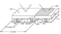
- FIG. 1is an isometric view depicting a portion of one embodiment of an interferometric modulator display in which a movable reflective layer of a first interferometric modulator is in a relaxed position and a movable reflective layer of a second interferometric modulator is in an actuated position.
- FIG. 2is a system block diagram illustrating one embodiment of an electronic device incorporating a 3 ⁇ 3 interferometric modulator display.
- FIG. 3is a diagram of movable mirror position versus applied voltage for one exemplary embodiment of an interferometric modulator of FIG. 1 .
- FIG. 4is an illustration of a set of row and column voltages that may be used to drive an interferometric modulator display.
- FIGS. 5A and 5Billustrate one exemplary timing diagram for row and column signals that may be used to write a frame of display data to the 3 ⁇ 3 interferometric modulator display of FIG. 2 .
- FIGS. 6A and 6Bare system block diagrams illustrating an embodiment of a visual display device comprising a plurality of interferometric modulators.
- FIG. 7Ais a cross section of the device of FIG. 1 .
- FIG. 7Bis a cross section of an alternative embodiment of an interferometric modulator.
- FIG. 7Cis a cross section of another alternative embodiment of an interferometric modulator.
- FIG. 7Dis a cross section of yet another alternative embodiment of an interferometric modulator.
- FIG. 7Eis a cross section of an additional alternative embodiment of an interferometric modulator.
- FIG. 8is a cross section of an embodiment of an unreleased interferometric modulator.
- FIGS. 9A-9Eare cross-sections illustrating the initial process steps in an embodiment of a method for making an array of interferometric modulators.
- FIGS. 10A-10Hare cross-sections illustrating the later process steps in the embodiment of a method for making an array of interferometric modulators.
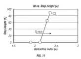
- FIG. 11is a graph depicting XeF 2 etch step height as a function of silicon-rich silicon nitride refractive index.
- the embodimentsmay be implemented in or associated with a variety of electronic devices such as, but not limited to, mobile telephones, wireless devices, personal data assistants (PDAs), hand-held or portable computers, GPS receivers/navigators, cameras, MP3 players, camcorders, game consoles, wrist watches, clocks, calculators, television monitors, flat panel displays, computer monitors, auto displays (e.g., odometer display, etc.), cockpit controls and/or displays, display of camera views (e.g., display of a rear view camera in a vehicle), electronic photographs, electronic billboards or signs, projectors, architectural structures, packaging, and aesthetic structures (e.g., display of images on a piece of jewelry).
- MEMS devices of similar structure to those described hereincan also be used in non-display applications such as in electronic switching devices.
- An embodimentprovides a method for making an interferometric modulator that involves the use of an etch stop between an upper electrode or reflective layer and a sacrificial layer.
- the etch stopcan be used to reduce undesirable over-etching of the sacrificial layer and the upper electrode or mirror layer.
- the etch stop layermay also serve as a barrier layer, buffer layer, and/or template layer.
- the etch stop layeris advantageously silicon-rich silicon nitride, which can be cleanly removed simultaneously with removal of the sacrificial layer.
- FIG. 1One interferometric modulator display embodiment comprising an interferometric MEMS display element is illustrated in FIG. 1 .
- the pixelsare in either a bright or dark state.
- the display elementIn the bright (“on” or “open”) state, the display element reflects a large portion of incident visible light to a user.
- the dark (“off” or “closed”) stateWhen in the dark (“off” or “closed”) state, the display element reflects little incident visible light to the user.
- the light reflectance properties of the “on” and “off” statesmay be reversed.
- MEMS pixelscan be configured to reflect predominantly at selected colors, allowing for a color display in addition to black and white.
- FIG. 1is an isometric view depicting two adjacent pixels in a series of pixels of a visual display, wherein each pixel comprises a MEMS interferometric modulator.
- an interferometric modulator displaycomprises a row/column array of these interferometric modulators.
- Each interferometric modulatorincludes a pair of reflective layers positioned at a variable and controllable distance from each other to form a resonant optical cavity with at least one variable dimension.
- one of the reflective layersmay be moved between two positions. In the first position, referred to herein as the relaxed position, the movable reflective layer is positioned at a relatively large distance from a fixed partially reflective layer.
- the movable reflective layerIn the second position, referred to herein as the actuated position, the movable reflective layer is positioned more closely adjacent to the partially reflective layer. Incident light that reflects from the two layers interferes constructively or destructively depending on the position of the movable reflective layer, producing either an overall reflective or non-reflective state for each pixel.
- the depicted portion of the pixel array in FIG. 1includes two adjacent interferometric modulators 12 a and 12 b .
- a movable reflective layer 14 ais illustrated in a relaxed position at a predetermined distance from an optical stack 16 a , which includes a partially reflective layer.
- the movable reflective layer 14 bis illustrated in an actuated position adjacent to the optical stack 16 b.
- optical stack 16typically comprise of several fused layers, which can include an electrode layer, such as indium tin oxide (ITO), a partially reflective layer, such as chromium, and a transparent dielectric.
- ITOindium tin oxide
- the optical stack 16is thus electrically conductive, partially transparent and partially reflective, and may be fabricated, for example, by depositing one or more of the above layers onto a transparent substrate 20 .
- the partially reflective layercan be formed from a variety of materials that are partially reflective such as various metals, semiconductors, and dielectrics.
- the partially reflective layercan be formed of one or more layers of materials, and each of the layers can be formed of a single material or a combination of materials.
- the layers of the optical stackare patterned into parallel strips, and may form row electrodes in a display device as described further below.
- the movable reflective layers 14 a , 14 bmay be formed as a series of parallel strips of a deposited metal layer or layers (orthogonal to the row electrodes of 16 a , 16 b ) deposited on top of posts 18 and an intervening sacrificial material deposited between the posts 18 . When the sacrificial material is etched away, the movable reflective layers 14 a , 14 b are separated from the optical stacks 16 a , 16 b by a defined gap 19 .
- a highly conductive and reflective materialsuch as aluminum may be used for the reflective layers 14 , and these strips may form column electrodes in a display device.
- the cavity 19remains between the movable reflective layer 14 a and optical stack 16 a , with the movable reflective layer 14 a in a mechanically relaxed state, as illustrated by the pixel 12 a in FIG. 1 .
- a potential differenceis applied to a selected row and column, the capacitor formed at the intersection of the row and column electrodes at the corresponding pixel becomes charged, and electrostatic forces pull the electrodes together.
- the movable reflective layer 14is deformed and is forced against the optical stack 16 .
- a dielectric layerwithin the optical stack 16 may prevent shorting and control the separation distance between layers 14 and 16 , as illustrated by pixel 12 b on the right in FIG. 1 .
- the behavioris the same regardless of the polarity of the applied potential difference. In this way, row/column actuation that can control the reflective vs. non-reflective pixel states is analogous in many ways to that used in conventional LCD and other display technologies.
- FIGS. 2 through 5Billustrate one exemplary process and system for using an array of interferometric modulators in a display application.
- FIG. 2is a system block diagram illustrating one embodiment of an electronic device that may incorporate aspects of the invention.
- the electronic deviceincludes a processor 21 which may be any general purpose single- or multi-chip microprocessor such as an ARM, Pentium®, Pentium II®, Pentium III®, Pentium IV®, Pentium® Pro, an 8051, a MIPS®, a Power PC®, an ALPHA®, or any special purpose microprocessor such as a digital signal processor, microcontroller, or a programmable gate array.
- the processor 21may be configured to execute one or more software modules.
- the processormay be configured to execute one or more software applications, including a web browser, a telephone application, an email program, or any other software application.
- the processor 21is also configured to communicate with an array driver 22 .
- the array driver 22includes a row driver circuit 24 and a column driver circuit 26 that provide signals to a display array or panel 30 .
- the cross section of the array illustrated in FIG. 1is shown by the lines 1 - 1 in FIG. 2 .
- the row/column actuation protocolmay take advantage of a hysteresis property of these devices illustrated in FIG. 3 . It may require, for example, a 10 volt potential difference to cause a movable layer to deform from the relaxed state to the actuated state. However, when the voltage is reduced from that value, the movable layer maintains its state as the voltage drops back below 10 volts.
- the movable layerdoes not relax completely until the voltage drops below 2 volts.
- There is thus a range of voltage, about 3 to 7 V in the example illustrated in FIG. 3where there exists a window of applied voltage within which the device is stable in either the relaxed or actuated state. This is referred to herein as the “hysteresis window” or “stability window.”
- hysteresis windowor “stability window.”
- the row/column actuation protocolcan be designed such that during row strobing, pixels in the strobed row that are to be actuated are exposed to a voltage difference of about 10 volts, and pixels that are to be relaxed are exposed to a voltage difference of close to zero volts. After the strobe, the pixels are exposed to a steady state voltage difference of about 5 volts such that they remain in whatever state the row strobe put them in. After being written, each pixel sees a potential difference within the “stability window” of 3-7 volts in this example. This feature makes the pixel design illustrated in FIG. 1 stable under the same applied voltage conditions in either an actuated or relaxed pre-existing state.
- each pixel of the interferometric modulatoris essentially a capacitor formed by the fixed and moving reflective layers, this stable state can be held at a voltage within the hysteresis window with almost no power dissipation. Essentially no current flows into the pixel if the applied potential is fixed.
- a display framemay be created by asserting the set of column electrodes in accordance with the desired set of actuated pixels in the first row.
- a row pulseis then applied to the row 1 electrode, actuating the pixels corresponding to the asserted column lines.
- the asserted set of column electrodesis then changed to correspond to the desired set of actuated pixels in the second row.
- a pulseis then applied to the row 2 electrode, actuating the appropriate pixels in row 2 in accordance with the asserted column electrodes.
- the row 1 pixelsare unaffected by the row 2 pulse, and remain in the state they were set to during the row 1 pulse. This may be repeated for the entire series of rows in a sequential fashion to produce the frame.
- the framesare refreshed and/or updated with new display data by continually repeating this process at some desired number of frames per second.
- protocols for driving row and column electrodes of pixel arrays to produce display framesare also well known and may be used in conjunction with the present invention.
- FIGS. 4 , 5 A, and 5 Billustrate one possible actuation protocol for creating a display frame on the 3 ⁇ 3 array of FIG. 2 .
- FIG. 4illustrates a possible set of column and row voltage levels that may be used for pixels exhibiting the hysteresis curves of FIG. 3 .
- actuating a pixelinvolves setting the appropriate column to ⁇ V bias , and the appropriate row to + ⁇ V, which may correspond to ⁇ 5 volts and +5 volts respectively Relaxing the pixel is accomplished by setting the appropriate column to +V bias , and the appropriate row to the same + ⁇ V, producing a zero volt potential difference across the pixel.
- the pixelsare stable in whatever state they were originally in, regardless of whether the column is at +V bias , or ⁇ V bias .
- voltages of opposite polarity than those described abovecan be used, e.g., actuating a pixel can involve setting the appropriate column to +V bias , and the appropriate row to ⁇ V.
- releasing the pixelis accomplished by setting the appropriate column to ⁇ V bias , and the appropriate row to the same ⁇ V, producing a zero volt potential difference across the pixel.
- FIG. 5Bis a timing diagram showing a series of row and column signals applied to the 3 ⁇ 3 array of FIG. 2 which will result in the display arrangement illustrated in FIG. 5A , where actuated pixels are non-reflective.
- the pixelsPrior to writing the frame illustrated in FIG. 5A , the pixels can be in any state, and in this example, all the rows are at 0 volts, and all the columns are at +5 volts. With these applied voltages, all pixels are stable in their existing actuated or relaxed states.
- pixels (1,1), (1,2), (2,2), (3,2) and (3,3)are actuated.
- columns 1 and 2are set to ⁇ 5 volts
- column 3is set to +5 volts. This does not change the state of any pixels, because all the pixels remain in the 3-7 volt stability window.
- Row 1is then strobed with a pulse that goes from 0, up to 5 volts, and back to zero. This actuates the (1,1) and (1,2) pixels and relaxes the (1,3) pixel. No other pixels in the array are affected.
- column 2is set to ⁇ 5 volts
- columns 1 and 3are set to +5 volts.
- Row 3is similarly set by setting columns 2 and 3 to ⁇ 5 volts, and column 1 to +5 volts.
- the row 3 strobesets the row 3 pixels as shown in FIG. 5A .
- the row potentialsare zero, and the column potentials can remain at either +5 or ⁇ 5 volts, and the display is then stable in the arrangement of FIG. 5A . It will be appreciated that the same procedure can be employed for arrays of dozens or hundreds of rows and columns.
- FIGS. 6A and 6Bare system block diagrams illustrating an embodiment of a display device 40 .
- the display device 40can be, for example, a cellular or mobile telephone.
- the same components of display device 40 or slight variations thereofare also illustrative of various types of display devices such as televisions and portable media players.
- the display device 40includes a housing 41 , a display 30 , an antenna 43 , a speaker 44 , an input device 48 , and a microphone 46 .
- the housing 41is generally formed from any of a variety of manufacturing processes as are well known to those of skill in the art, including injection molding, and vacuum forming.
- the housing 41may be made from any of a variety of materials, including but not limited to plastic, metal, glass, rubber, and ceramic, or a combination thereof.
- the housing 41includes removable portions (not shown) that may be interchanged with other removable portions of different color, or containing different logos, pictures, or symbols.
- the display 30 of the exemplary display device 40may be any of a variety of displays, including a bi-stable display, as described herein.
- the display 30includes a flat-panel display, such as plasma, EL, OLED, STN LCD, or TFT LCD as described above, or a non-flat-panel display, such as a CRT or other tube device, as is well known to those of skill in the art.
- the display 30includes an interferometric modulator display, as described herein.
- the components of one embodiment of exemplary display device 40are schematically illustrated in FIG. 6B .
- the illustrated exemplary display device 40includes a housing 41 and can include additional components at least partially enclosed therein.
- the exemplary display device 40includes a network interface 27 that includes an antenna 43 which is coupled to a transceiver 47 .
- the transceiver 47is connected to a processor 21 , which is connected to conditioning hardware 52 .
- the conditioning hardware 52may be configured to condition a signal (e.g., filter a signal).
- the conditioning hardware 52is connected to a speaker 45 and a microphone 46 .
- the processor 21is also connected to an input device 48 and a driver controller 29 .
- the driver controller 29is coupled to a frame buffer 28 , and to an array driver 22 , which in turn is coupled to a display array 30 .
- a power supply 50provides power to all components as required by the particular exemplary display device 40 design.
- the network interface 27includes the antenna 43 and the transceiver 47 so that the exemplary display device 40 can communicate with one ore more devices over a network. In one embodiment the network interface 27 may also have some processing capabilities to relieve requirements of the processor 21 .
- the antenna 43is any antenna known to those of skill in the art for transmitting and receiving signals. In one embodiment, the antenna transmits and receives RF signals according to the IEEE 802.11 standard, including IEEE 802.11(a), (b), or (g). In another embodiment, the antenna transmits and receives RF signals according to the BLUETOOTH standard. In the case of a cellular telephone, the antenna is designed to receive CDMA, GSM, AMPS or other known signals that are used to communicate within a wireless cell phone network.
- the transceiver 47pre-processes the signals received from the antenna 43 so that they may be received by and further manipulated by the processor 21 .
- the transceiver 47also processes signals received from the processor 21 so that they may be transmitted from the exemplary display device 40 via the antenna 43 .
- the transceiver 47can be replaced by a receiver.
- the network interface 27can be replaced by an image source, which can store or generate image data to be sent to the processor 21 .
- the image sourcecan be a digital video disc (DVD) or a hard-disc drive that contains image data, or a software module that generates image data.
- the processor 21generally controls the overall operation of the exemplary display device 40 .
- the processor 21receives data, such as compressed image data from the network interface 27 or an image source, and processes the data into raw image data or into a format that is readily processed into raw image data.
- the processor 21then sends the processed data to the driver controller 29 or to the frame buffer 28 for storage.
- Raw datatypically refers to the information that identifies the image characteristics at each location within an image. For example, such image characteristics can include color, saturation, and gray-scale level.
- the processor 21includes a microcontroller, CPU, or logic unit to control operation of the exemplary display device 40 .
- the conditioning hardware 52generally includes amplifiers and filters for transmitting signals to the speaker 45 , and for receiving signals from the microphone 46 .
- the conditioning hardware 52may be discrete components within the exemplary display device 40 , or may be incorporated within the processor 21 or other components.
- the driver controller 29takes the raw image data generated by the processor 21 either directly from the processor 21 or from the frame buffer 28 and reformats the raw image data appropriately for high speed transmission to the array driver 22 . Specifically, the driver controller 29 reformats the raw image data into a data flow having a raster-like format, such that it has a time order suitable for scanning across the display array 30 . Then the driver controller 29 sends the formatted information to the array driver 22 .
- a driver controller 29such as a LCD controller, is often associated with the system processor 21 as a stand-alone Integrated Circuit (IC), such controllers may be implemented in many ways. They may be embedded in the processor 21 as hardware, embedded in the processor 21 as software, or filly integrated in hardware with the array driver 22 .
- ICIntegrated Circuit
- the array driver 22receives the formatted information from the driver controller 29 and reformats the video data into a parallel set of waveforms that are applied many times per second to the hundreds and sometimes thousands of leads coming from the display's x-y matrix of pixels.
- the driver controller 29 , array driver 22 , and display array 30are appropriate for any of the types of displays described herein.
- the driver controller 29is a conventional display controller or a bi-stable display controller (e.g., an interferometric modulator controller).
- the array driver 22is a conventional driver or a bi-stable display driver (e.g., an interferometric modulator display).
- the driver controller 29is integrated with the array driver 22 .
- display array 30is a typical display array or a bi-stable display array (e.g., a display including an array of interferometric modulators).
- the input device 48allows a user to control the operation of the exemplary display device 40 .
- the input device 48includes a keypad, such as a QWERTY keyboard or a telephone keypad, a button, a switch, a touch-sensitive screen, a pressure- or heat-sensitive membrane.
- the microphone 46is an input device for the exemplary display device 40 . When the microphone 46 is used to input data to the device, voice commands may be provided by a user for controlling operations of the exemplary display device 40 .
- the power supply 50can include a variety of energy storage devices as are well known in the art.
- the power supply 50is a rechargeable battery, such as a nickel-cadmium battery or a lithium ion battery.
- the power supply 50is a renewable energy source, a capacitor, or a solar cell, including a plastic solar cell, and solar-cell paint.
- the power supply 50is configured to receive power from a wall outlet.
- control programmabilityresides, as described above, in a driver controller which can be located in several places in the electronic display system. In some cases control programmability resides in the array driver 22 . Those of skill in the art will recognize that the above-described optimization may be implemented in any number of hardware and/or software components and in various configurations.
- FIGS. 7A-7Eillustrate five different embodiments of the movable reflective layer 14 and its supporting structures.
- FIG. 7Ais a cross section of the embodiment of FIG. 1 , where a strip of metal material 14 is deposited on orthogonally extending supports 18 .
- FIG. 7Bthe moveable reflective layer 14 is attached to supports 18 at the corners only, on tethers 32 .
- FIG. 7Cthe moveable reflective layer 14 is suspended from a deformable layer 34 , which may comprise a flexible metal.
- the deformable layer 34connects, directly or indirectly, to the substrate 20 around the perimeter of the deformable layer 34 .
- the connectionsare herein referred to as supports or posts 18 .
- the embodiment illustrated in FIG. 7Dhas supports 18 including support post plugs 42 upon which the deformable layer 34 rests.
- the movable reflective layer 14remains suspended over the cavity, as in FIGS. 7A-7C , but the deformable layer 34 does not form the support posts by filling holes between the deformable layer 34 and the optical stack 16 . Rather, the support posts are formed of a planarization material, which is used to form support post plugs 42 .
- the embodiment illustrated in FIG. 7 Eis based on the embodiment shown in FIG. 7D , but may also be adapted to work with any of the embodiments illustrated in FIGS. 7A-7C as well as additional embodiments not shown. In the embodiment shown in FIG. 7E , an extra layer of metal or other conductive material has been used to form a bus structure 44 . This allows signal routing along the back of the interferometric modulators, eliminating a number of electrodes that may otherwise have had to be formed on the substrate 20
- the interferometric modulatorsfunction as direct-view devices, in which images are viewed from the front side of the transparent substrate 20 , the side opposite to that upon which the modulator is arranged.
- the reflective layer 14optically shields the portions of the interferometric modulator on the side of the reflective layer opposite the substrate 20 , including the deformable layer 34 . This allows the shielded areas to be configured and operated upon without negatively affecting the image quality.
- Such shieldingallows the bus structure 44 in FIG. 7E , which provides the ability to separate the optical properties of the modulator from the electromechanical properties of the modulator, such as addressing and the movements that result from that addressing.
- This separable modulator architectureallows the structural design and materials used for the electromechanical aspects and the optical aspects of the modulator to be selected and to function independently of each other. Moreover, the embodiments shown in FIGS. 7C-7E have additional benefits deriving from the decoupling of the optical properties of the reflective layer 14 from the mechanical properties of the modulator, which are carried out by the deformable layer 34 . This allows the structural design and materials used for the reflective layer 14 to be optimized with respect to the optical properties, and the structural design and materials used for the deformable layer 34 to be optimized with respect to desired mechanical properties.
- interferometric modulatorssuch as those depicted in FIGS. 7A-7E , may be manufactured by using a sacrificial layer to define the air gaps.
- the sacrificial layermay be removed by etching (herein referred to as “releasing” an interferometric modulator).
- Suitable materials for the sacrificial layerinclude, but are not limited to, molybdenum, germanium, tungsten, and amorphous silicon.
- FIG. 8is a cross-sectional view illustrating an embodiment of an unreleased interferometric modulator 100 comprising a sacrificial layer 102 , an upper reflective layer 14 over the sacrificial layer 102 , and an etch stop layer 104 between the sacrificial layer 102 and the upper reflective layer 14 .
- a similar structuremay be used for other MEMS devices where upper reflective layer 14 is generally an electrode layer that is preferably movable upon removal of the sacrificial layer 102 .
- the unreleased interferometric modulator 100corresponds to the released interferometric modulator depicted in FIG. 7D (i.e., the interferometric modulator of FIG.
- the etch stop layer 104may be used to protect the sacrificial layer 102 during patterning of the reflective layer 14 .
- the etchant used to pattern the reflective layer 14e.g., a PAN etchant
- the etchant used to pattern the reflective layer 14may also partially etch the underlying sacrificial layer 102 unless the etch stop layer 104 is included.
- a PAN etchantmay also partially etch the underlying sacrificial layer 102 unless the etch stop layer 104 is included.
- the thickness of the etch stop layer 104may be in the range of about 100 ⁇ to about 700 ⁇ . In some embodiments, the thickness of the etch stop layer 104 is in the range of about 300 ⁇ to about 700 ⁇ .
- Etch stop layers 104consisting of SiO 2 or titanium may be used, for example, as discussed more fully in co-pending U.S. application Ser. No. 11/090,773, filed Mar. 25, 2005, which is incorporated herein by reference in its entirety. However, SiO 2 is not completely removed by the XeF 2 used to remove the sacrificial layer 102 , leaving undesired residue on the reflective layer 14 . Use of titanium tends to distort the flatness of an aluminum reflective layer 14 .
- the etch stop layer 104comprises a silicon-rich silicon nitride.
- the silicon-rich silicon nitride etch stop layer 104may be removed during the release etch that removes the sacrificial layer.
- silicon-rich silicon nitriderefers to any silicon nitride material that has a ratio of silicon to nitrogen greater than the typical stoichiometric silicon nitride ratio of about 3:4.
- the silicon-rich silicon nitride etch stop layercan be formed by chemical vapor deposition (e.g., at low temperature by plasma enhanced chemical vapor deposition) or any other suitable means.
- the silicon-rich silicon nitridehas a silicon to nitrogen ratio of greater than about 1:1.
- silicon nitride filmsare provided that have a refractive index of greater than about 2.1. More preferably, silicon nitride films are provided that have a refractive index of greater than about 2.2.
- the upper reflective layer 14(or other movable electrode layer for MEMS devices other than interferometric modulators) may be aluminum.
- the upper reflective layer 14may be a material that comprises aluminum and thus may be an aluminum alloy such as, for example, Al—Si, Al—Cu, Al—Ti, or Al—Nd.
- the sacrificial layer 102comprises molybdenum in the illustrated embodiment.
- Other suitable sacrificial materialsinclude, but are not limited to, amorphous silicon (“a-Si”), germanium, and tungsten.
- the etch stop layer 104also acts as a diffusion barrier to prevent interdiffusion between the material in the sacrificial layer 102 and the upper reflective layer 14 .
- an etch stop layer 104 of silicon-rich silicon nitridewill prevent interdiffusion between the aluminum in the upper reflective layer 14 and the silicon in the sacrificial layer 102 .
- the materials used for the fabrication of the sacrificial layer 102 , the reflective layer 14 , and the etch stop layer 104are selected in combination with one another to bring about certain desired effects such as etch selectivity, resistance to diffusion (diffusion barrier), barrier to crystallographic influence, and crystallographic templating, as described in greater detail below.
- the upper reflective layer 14 and etch stop layer 104are spaced from a glass substrate 20 by posts 18 , which in the illustrated embodiment include support plugs 42 . In other embodiments, the upper reflective layer 14 may be supported by other structures, including side walls, such as for example is depicted in FIG. 7C .
- the unreleased interferometric modulator 100also includes a transparent electrode layer 106 over the glass substrate 20 .
- the electrode layer 106may comprise a transparent metal film such as indium tin oxide (ITO) or zinc tin oxide (ZTO).
- a lower reflective layer 108such as chrome or molybdenum
- a dielectric layer 110such as a SiO 2 or a composite layer comprising a layer of SiO 2 and a layer of Al 2 O 3
- the electrode layer 106 , lower reflective layer 108 , and dielectric layer 110may together be referred to as an optical stack 16 that partially transmits and partially reflects light.
- the etch stop layer 104may be included in other unreleased interferometric modulator configurations, e.g., any of the configurations resulting in the interferometric modulators illustrated in FIGS. 7A-7E .
- the presence of an etch stop layer between the upper reflective layer and the sacrificial layermay significantly improve one or more aspects of various processes for making interferometric modulators (including arrays thereof), and/or may improve one or more qualities of the resulting interferometric modulators themselves.
- the etch stop layer 104may comprise or serve as an etch stop as described below with reference to FIGS. 9A-10H in the context of making an array of interferometric modulators of the general type illustrated in FIG. 7D .
- etch stop layersmay be used to manufacture other MEMS devices, including interferometric modulators of the general types illustrated in FIGS. 7A-7E , as well as other types of spatial light modulators.
- the etch stop layermay be used between a layer used to define a cavity (e.g., sacrificial layer 102 c ) and a structure adjacent to the cavity (e.g., a movable electrode such as reflective layer 14 ) in any MEMS device.
- a cavitye.g., sacrificial layer 102 c
- a structure adjacent to the cavitye.g., a movable electrode such as reflective layer 14
- FIGS. 9A-10Hmay refer to particular steps, sequences, and materials, it is understood that such details are for the purpose of illustration, and that other steps, sequences and/or materials may be used.
- FIGS. 9A-9Eare cross-sectional views illustrating the initial steps in a process for manufacturing an array of unreleased interferometric modulators (release by removal of the sacrificial material to form interferometric modulators is discussed below with reference to FIGS. 10A-10H ).
- FIGS. 9A-10Hthe formation of an array of three interferometric modulators 200 (red subpixel), 202 (green subpixel), and 204 (blue subpixel) are illustrated.
- Each of the interferometric modulators 200 , 202 , and 204have a different distance between the lower reflective layer 108 and the upper reflective layer 14 as indicated in FIG. 10H , which shows final configurations.
- Color displaysmay be formed by using three (or more) modulator elements to form each pixel in the resulting image.
- the dimensions of each interferometric modulator cavitydetermine the nature of the interference and the resulting color.
- One method of forming color pixelsis to construct arrays of interferometric modulators, each having cavities of differing sizes, e.g., three different sizes corresponding to red, green and blue as shown in this embodiment.
- the interference properties of the cavitiesare directly affected by their dimensions.
- multiple sacrificial layer thicknessesmay be fabricated as described below so that the resulting pixels reflect light corresponding to each of the three primary colors. Other color combinations are also possible, as well as the use of black and white pixels.
- FIG. 9Aillustrates an optical stack 16 formed by depositing an indium tin oxide electrode layer 106 on a transparent substrate 20 and then depositing a first reflective layer 108 on the electrode layer 106 .
- the first reflective layer 108comprises chrome.
- Other reflective metalssuch as molybdenum and titanium may also be used to form the first reflective layer 108 .
- FIGS. 9A-10Halthough the electrode layer 106 and the first reflective layer 108 are indicated as a single layer 106 , 108 , it is understood that for an interferometric modulator embodiment, the first reflective layer 108 is formed on the electrode layer 106 as illustrated in FIG. 8 . In other MEMS devices, only a single electrode layer may be required.
- the viewing surface 120 of the transparent substrate 20is on the opposite side of the substrate 20 from the first reflective layer 108 and the electrode layer 106 .
- the electrode and first reflective layers 106 , 108are patterned and etched to form electrode columns, rows, or other useful shapes as required by the display design.
- the optical stack 16also includes an oxide dielectric layer 110 over the reflective layer 108 , typically formed after the electrode and first reflective layers 106 , 108 have been patterned and etched.
- FIG. 9Afurther illustrates a first subpixel sacrificial layer 102 a formed by depositing molybdenum over the optical stack 16 (and thus over the oxide dielectric layer 110 , first reflective layer 108 , and electrode layer 106 ).
- the molybdenumis etched to form the first pixel sacrificial layer 102 a , thereby exposing a portion 110 a of the oxide dielectric layer 110 that is the region where the resulting green and blue interferometric modulators 202 and 204 are formed ( FIG. 10H ).
- the thickness of the first sacrificial layer 102 a(along with the thicknesses of subsequently deposited layers as described below) influences the size of the corresponding cavity 206 in the resulting red interferometric modulator 200 ( FIG. 10H ).
- FIGS. 9B-9Cillustrate forming a second subpixel sacrificial layer 102 b by deposition, masking, and patterning over the exposed portion 110 a of the oxide dielectric layer 110 and the first subpixel sacrificial layer 102 a .
- the second subpixel sacrificial layer 102 bpreferably comprises the same sacrificial material as the first subpixel sacrificial layer 102 a (molybdenum in this embodiment).
- the second subpixel sacrificial layer 102 bis patterned and etched as illustrated in FIG. 9C to expose a portion 110 b f the oxide dielectric layer 110 in the region where the resulting blue interferometric modulator 204 will be formed ( FIG. 10H ).
- a third subpixel sacrificial layer 102 cis then deposited over the exposed portion 110 of the oxide dielectric layer 110 and the second subpixel sacrificial layer 102 b as illustrated in FIG. 9D .
- the third subpixel sacrificial layer 102 cneed not be patterned or etched in this embodiment, since its thickness will influence the sizes of all three cavities 206 , 208 , and 210 in the resulting interferometric modulators 200 , 202 , and 204 ( FIG. 10H ).
- the three deposited subpixel sacrificial layers 102 a , 102 b , and 102 cdo not necessarily have the same thickness.
- the thicknesses of the sacrificial layers 102 a , 102 b , and 102 ccumulatively define the air gap 206 of the red subpixel 200 ( FIG. 10H ).
- the thicknesses of the sacrificial layers 102 b and 102 ccumulatively define the air gap 208 of the green subpixel 202 ( FIG. 10H ).
- the thickness of the sacrificial layer 102 cdefines the air gap 210 of the blue subpixel 204 ( FIG. 10H ).
- FIG. 9Eillustrates forming an etch stop layer 104 by depositing silicon-rich silicon nitride as described above over the third subpixel sacrificial layer 102 c , followed by depositing a second reflective layer 14 (e.g., an aluminum-containing metal) over the etch stop layer 104 .
- the second reflective layer 14also serves as an electrode.
- the second reflective layer 14is preferably deposited immediately or very soon after the etch stop layer 104 is deposited.
- the second reflective layer 14is deposited over the etch stop layer 104 immediately after depositing the etch stop layer 104 , preferably in the same deposition chamber and without breaking a vacuum, resulting in reduced oxidation of the surface of the second reflective layer 14 .
- the thickness of the etch stop layer 104may be in the range of about 100 ⁇ to about 700 ⁇ , preferably in the range of about 100 ⁇ to about 300 ⁇ .
- the thickness of the etch step layeris preferably in the range of from about 300 ⁇ to about 700 ⁇ .
- FIGS. 10A-10Hare cross-sectional views illustrating various later steps following the process steps illustrated in FIGS. 9A-9E .
- the second reflective layer 14(comprising aluminum in this embodiment) has been patterned and etched using an appropriate etch chemistry for the removal of the metal.
- etch chemistriesare known to those skilled in the art.
- a PAN etchantaqueous phosphoric acid/acetic acid/nitric acid
- Remaining portions 14 a , 14 b , and 14 c of the second reflective layer 14are protected by a mask (not shown) and thus are not removed during etching.
- the etch stop layer 104protects the underlying third sacrificial layer 102 c from being etched. Etching of the second reflective layer 14 to form the portions 14 a , 14 b , and 14 c exposes portions 104 a of the etch stop layer 104 . Unexposed portions 104 b of the etch stop layer 104 underlie the remaining second reflective layer portions 14 a , 14 b , and 14 c . The exposed portions 104 a of the etch stop layer 104 may then optionally be removed ( FIG.
- etchingby further etching using a different etch chemistry (e.g., a hydrofluoric acid (HF) etchant or buffered oxide etchants (BOE) (i.e., blends of HF and ammonium fluoride)) that does not remove the third sacrificial layer 102 c so that the portions 104 b underlying the remaining metal reflective layer 14 a , 14 b , and 14 c remain. Removal of the exposed portions 104 a of the etch stop layer 104 ensures that no etch stop layer 104 material remains between sacrificial layers.
- a different etch chemistrye.g., a hydrofluoric acid (HF) etchant or buffered oxide etchants (BOE) (i.e., blends of HF and ammonium fluoride)
- FIG. 10Billustrates the formation of a fourth sacrificial layer 102 d over the patterned second reflective layer 14 a , 14 b , and 14 c and the third sacrificial layer 102 c .
- FIG. 10Cillustrates forming connector holes 122 a and post holes 122 b by patterning and etching the sacrificial layers 102 a , 102 b , 102 c , and 102 d .
- a planarization material 124is optionally applied to fill in the connector holes 122 a and post holes 122 b .
- planarization materialsinclude, but are not limited to, silicon dioxide, silicon nitride, organic materials (e.g., epoxies, acrylics, and vinyl-based chemistries), and silicon- or metal-containing organometallics.
- various polyimides, low-k materials, and spin-on glassesmay be used.
- FIG. 10Eillustrates forming a mechanical film (flex or deformable layer) 34 by depositing a flexible material such as a metal over the planarization material 124 and the fourth sacrificial layer 102 d , followed by patterning and etching the mechanical layer 34 to form columns or rows such that an array of unreleased interferometric modulators 130 is formed ( FIG. 10F ).
- the planarization material 124is not used, in which case the connector holes 122 a and post holes 122 b may be filled with the same material that is used to form the mechanical layer 34 .
- FIG. 10Gillustrates removing the sacrificial layers 102 a , 102 b , 102 c , and 102 d to form the cavities 206 , 208 , 210 , thereby exposing the portion 104 b of the etch stop layer 104 underlying the remaining portions 14 a , 14 b , and 14 c of the reflective layer 14 .
- the etch stop layer 104 a underlying the second reflective layers 14 a , 14 b , and 14 c that is exposed by the removal of the sacrificial layers 102 a , 102 b , 102 cmay be used to protect the second reflective layers 14 a , 14 b , and 14 c during the etching of the sacrificial layers 102 a , 102 b , 102 c , and 102 d .
- etchantsmay be used that etch the sacrificial layer material but not the etch stop layer material. For example, most wet etchants that etch molybdenum do not etch silicon nitrides.
- the planarization material 42is not removed by the etchant and thus remains to form posts 42 ( FIG. 10H ).
- the etch stop layer 104 b underlying the second reflective layer 14 a , 14 b , and 14 cmay then itself be removed by etching using an appropriate etch chemistry (e.g., SF 6 plasma etch) as illustrated in FIG. 10H , thereby exposing the mirror surface of the second reflective layer 14 a , 14 b , and 14 c.
- an appropriate etch chemistrye.g., SF 6 plasma etch
- gaseous or vaporous XeF 2is used as an etchant to remove both the molybdenum sacrificial layers 46 a , 46 b , 46 c , 46 d and the etch stop layer 104 b simultaneously.
- gaseous or vaporous XeF 2is used as an etchant to remove both the molybdenum sacrificial layers 46 a , 46 b , 46 c , 46 d and the etch stop layer 104 b simultaneously.
- silicon-rich silicon nitridemay be completely removed using a XeF 2 etch.
- XeF 2may serve as a source of fluorine-containing gases such as F 2 and HF, and thus F 2 or HF may be used in place of or in addition to XeF 2 as an etchant for the preferred sacrificial materials, including molybdenum, amorphous silicon, germanium, and tungsten.
- FIGS. 10H and 9Eillustrates that the size of the cavity 206 ( FIG. 10H ) corresponds to the combined thicknesses of the three sacrificial layers 102 a , 102 b , and 102 c and the etch stop layer 104 .
- the size of the cavity 208corresponds to the combined thickness of two sacrificial layers 102 b and 102 c and the etch stop layer 104
- the size of the cavity 210corresponds to the combined thicknesses of the sacrificial layer 102 c and the etch stop layer 104 .
- the dimensions of the cavities 206 , 208 , and 210vary according to the various combined thicknesses of the four layers 102 a , 102 b , 102 c , and 104 , resulting in an array of interferometric modulators 200 , 202 , and 204 capable of displaying three different colors such as red, green and blue.
- the materials used for the fabrication of the sacrificial layer(s) 102 , the reflective layer 14 , and the etch stop layer 104are preferably selected in combination with one another to bring about certain desired effects.
- the etch stop layer 104also serves as a diffusion barrier layer that slows diffusion of metal from the reflective layer 14 into the sacrificial material 102 . It has been found that such diffusion is often undesirable because it tends to blur the boundary between the reflective layer and the sacrificial layer, resulting in reduced etch selectivity during processing and reduced mirror quality in the resulting interferometric modulator.
- the etch stop layer/barrier layer 104preferably has a thickness in the range of about 300 ⁇ to about 700 ⁇ .
- the etch stop layer 104also serves as a buffer layer that substantially prevents a crystallographic orientation of the sacrificial material 102 from producing a corresponding crystallographic orientation in the reflective layer 14 . It has been found that some materials used to form the sacrificial layer display a crystallographic orientation after deposition and/or subsequent processing steps.
- molybdenumis a crystalline material having a crystallographic orientation (typically body centered cubic) on any particular surface that results from the crystalline lattice spacing of the molybdenum atoms.
- the depositing metalmay tend to follow the crystallographic orientation of the underlying molybdenum, producing a corresponding crystallographic orientation in the reflective layer 14 .
- the lattice spacing of the resulting deposited metal layeris often different than it would be in the absence of the underlying molybdenum, and in many cases the deposited metal layer is mechanically strained as a result.
- the as-deposited lattice spacing of the metal atomsmay relax to the natural lattice spacing for the metal, in some cases changing the dimensions of the reflective layer and producing undesirable warping.
- the etch stop layer/buffer layer 104is preferably amorphous or does not have the same lattice spacing as the underlying sacrificial layer 102 .
- silicon-rich silicon nitrideis typically amorphous.
- the metal atomsdeposit on the etch stop layer/buffer layer 104 rather than on the underlying sacrificial layer 102 , and the buffer layer substantially prevents a crystallographic orientation of the sacrificial layer 104 from producing a corresponding crystallographic orientation in the reflective layer 14 .
- the etch stop layer 104 balso serves as a template layer having a crystalline orientation that is substantially similar to a crystallographic orientation of the reflective layer 14 .
- a depositing metalmay tend to follow the crystallographic orientation of the underlying layer, producing a corresponding crystallographic orientation in the metal layer. This tendency may be used to advantage by selecting, for use as an etch stop layer 104 , a material that has a crystallographic orientation that would be desirable to impart to the reflective layer 14 .
- An etch stop layer 104 formed of such a materialthus serves as a crystallographic template that produces a substantially similar crystalline orientation in the subsequently deposited reflective layer 14 .
- the processing steps used to fabricate the interferometric modulators and arrays thereof described hereinare preferably selected in combination with the materials used for the fabrication of the sacrificial layer 102 , the reflective layer 14 , and the etch stop layer 104 to bring about certain desired effects.
- the etch stop layer 104protects the underlying third sacrificial layer 102 c from being etched.
- the etch stop layer 104 b(underlying the second electrode or mirror layers 14 a , 14 b , and 14 c ) that is exposed by the removal of the sacrificial layers 102 a , 102 b , 102 c protects the second mirror layers 14 a , 14 b , and 14 c during the etching of the sacrificial layers 102 a , 102 b , 102 c , 102 d .
- the etch stop layer 104may protect a sacrificial layer and/or a reflective layer from being etched during the removal of some other layer.
- the material being etchedis preferably removed at a rate that is at least about 10 times faster than the rate at which the etch stop layer is removed, preferably at least about 20 times faster.
- the aluminum in the second reflective layer 14is preferably removed by the etchant at a rate that is at least about 10 times faster than the rate at which the material in the etch stop layer 104 is removed by the etchant, and more preferably at least about 20 times faster.
- the material in the sacrificial layersis preferably removed at a rate that is at least about 10 times faster than the rate at which the material in the etch stop layer 104 is removed, and more preferably at least about 20 times faster.
- the portions 104 b of the etch stop layer 104 underlying the second electrode or reflective layer portions 14 a , 14 b , and 14 cmay be selectively removed by etching to expose the mirror surfaces of the second reflective layer portions 14 a , 14 b , and 14 c in a manner that minimizes damage to the mirror surfaces.
- the etchantpreferably removes the portions 104 b of the etch stop layer 104 at a rate that is at least about 10 times faster than a rate at which the etchant removes the second mirror reflective layer portions 14 a , 14 b , and 14 c , more preferably at least about 20 times faster.
- the above embodimentsare not intended to limit the present invention, and the methods described herein may be applied to any structure in which two materials having similar etching profiles are used in a proximate area and subjected to etching where selective etching is desired.
- the methods described hereinmay be applied to increase etch selectivity between combinations of an Al-containing material and a Mo-containing material. No structural limitation or restriction is imposed or intended. Further, no limitation or restriction is imposed or intended on the particular formation sequence.
- interferometric modulatorsmay use conventional semiconductor manufacturing techniques such as photolithography, deposition (e.g., “dry” methods such as chemical vapor deposition (CVD) and wet methods such as spin coating), masking, etching (e.g., dry methods such as plasma etch and wet methods), etc.
- depositione.g., “dry” methods such as chemical vapor deposition (CVD) and wet methods such as spin coating
- maskinge.g., dry methods such as plasma etch and wet methods
- etchinge.g., dry methods such as plasma etch and wet methods
- a thin film of standard silicon nitride (silicon to nitrogen ratio of 3:4) formed on a substratewas tested for sensitivity to various etchants including PAD, PAN and XeF 2 etchants.
- a test pattern maskwas applied to the standard silicon nitride films and the films were exposed to the etchants. After removing the pattern mask, any resulting step height was measured to determine sensitivity to the etchants.
- Exposure to the PAD etchantwas at room temperature for a 10 minute soak.
- the standard silicon nitride filmwas only very slightly etched by the PAD etchant.
- Exposure to XeF 2consisted of using two cycles of 120 s of gas fill time followed by 300 s of etching time.
- Test waferswere constructed using five different deposition conditions to form various silicon nitride films on glass or silicon wafers.
- the silicon nitride filmswere formed by Micralyne, Inc. of Edmonton Alberta using plasma enhanced chemical vapor deposition (PECVD) by reaction between SiH 4 and NH 3 . All silicon nitride films were formed at a pressure of 90° mTorr and a temperature of 350° C. RE power for generating the plasma was 20 W.
- the gas flow rates, deposition rates (DR), and measured refractive indices (RI) of the resulting filmsare indicated in Table 1.
- the sensitivities of these test films to etching by XeF 2 and PAN etchantswere determined by applying a test pattern mask and then exposing the films to the respective etchants. The pattern mask was then removed and any resulting step heights measured.
- the XeF 2 etch testconsisted of exposing the five films formed on glass wafers to two cycles of 120 s XeF 2 gas fill time followed by 300 s of etch time.
- the PAN etch testconsisted of soaking the five films formed on silicon wafers in PAN etchant for 10 minutes. The PAN etchant resulted in no observable etching of any of the silicon nitride films. In contrast, the silicon-rich silicon nitride films (e.g., those formed by reaction conditions 2-5) were sensitive to XeF 2 etching. Table 2 lists the observed step heights formed from XeF 2 etching of the test pattern.
- FIG. 11depicts a graph showing the observed step height as a function of refractive index. Also included in the graph is the standard silicon nitride tested in Example 1, with a refractive index of about 1.9. This data indicates that as the refractive index increases, the sensitivity to XeF 2 etching generally increases.
- the refractive index of standard silicon nitridei.e., a 3:4 ratio of silicon to nitrogen
- the refractive index of pure siliconis 3.7. Accordingly, increasing refractive indices above 2.1 indicate increasing amounts of silicon in the silicon nitride films (e.g., silicon-rich silicon nitride).
- silicon-rich silicon nitride filmsare sensitive to XeF 2 etching and can therefore be cleanly removed during XeF 2 release etching in interferometric modulators.
- Test waferswere constructed using four different deposition conditions to form various silicon nitride films on glass or silicon substrates.
- the silicon nitride filmswere formed using plasma enhanced chemical vapor deposition by reaction between SiH 4 and NH 3 . All silicon nitride films were formed at a pressure of 650 mTorr. RF power for generating the plasma was 25 W.
- the gas flow rates, temperature, deposition rates (DR), and measured refractive indices (RI) of the resulting filmsare indicated in Table 3.
- Condition 1corresponds to deposition conditions resulting in standard silicon nitride (i.e., a silicon to nitrogen ratio of 3:4).
- Condition 4corresponds to the standard conditions except for a lower reaction temperature. Increasing the ratio of the SiH 4 reactant to NH 3 resulted in an increase in refractive index, indicating an increase in the silicon content of the resulting film.
- the sensitivities of these test films to etching by XeF 2 and PAN etchantswere determined by applying a test pattern mask and then exposing the films to the respective etchants. The pattern mask was then removed and any resulting step heights measured.
- the XeF 2 etch testconsisted of exposing the four films to four cycles of 120 s XeF 2 gas fill time followed by 300 s of etch time.
- the PAN etch testconsisted of soaking the four films in PAN etchant for 10 minutes. The PAN etchant resulted in no observable etching of the silicon nitride films. On glass wafers, standard silicon nitride (e.g., wafer no.
- silicon nitride filmswere sensitive to XeF 2 etching on a silicon substrate, however, standard silicon nitride (e.g., wafer no. 1) was not completely removed. In contrast, the silicon-rich silicon nitride films on silicon substrates were completely removed upon XeF 2 etching.
Landscapes
- Physics & Mathematics (AREA)
- Engineering & Computer Science (AREA)
- Manufacturing & Machinery (AREA)
- Microelectronics & Electronic Packaging (AREA)
- Spectroscopy & Molecular Physics (AREA)
- General Physics & Mathematics (AREA)
- Optics & Photonics (AREA)
- Mechanical Light Control Or Optical Switches (AREA)
- Micromachines (AREA)
Abstract
Description
| TABLE 1 |
| Reaction conditions for silicon nitride test wafers. |
| Wafer | SiH4 | NH3 | N2 | DR | ||
| No. | (sccm) | (sccm) | SiH4/NH3 | (sccm) | (Å/min) | |
| 1 | 40 | 40 | 1 | 1960 | 118 | 2.12 |
| 2 | 80 | 40 | 2 | 1960 | 169 | 2.45 |
| 3 | 40 | 20 | 2 | 1960 | 151 | 2.35 |
| 4 | 60 | 40 | 1.5 | 1960 | 142 | 2.28 |
| 5 | 40 | 10 | 4 | 1960 | 213 | N/A |
| TABLE 2 |
| Step heights caused by XeF2etching. |
| Wafer No. | Step Height (Å) | ||
| 1 | 0 | ||
| 2 | 87 | ||
| 3 | 89 | ||
| 4 | 65 | ||
| 5 | 73 | ||
| TABLE 3 |
| Reaction conditions for silicon nitride test wafers. |
| Wafer | NH3 | SiH4 | T | DR | Film Thickness | |
| No. | (sccm) | (sccm) | (° C.) | RI | (Å/min) | (Å) |
| 1 | 35 | 40 | 350 | 2.07 | 93.1 | 931 |
| 2 | 20 | 40 | 350 | 2.32 | 78.7 | 787 |
| 3 | 10 | 40 | 350 | 3 | 59.2 | 592 |
| 4 | 35 | 40 | 250 | 2.03 | 95.9 | 959 |
Claims (3)
Priority Applications (1)
| Application Number | Priority Date | Filing Date | Title |
|---|---|---|---|
| US12/128,469US8064124B2 (en) | 2006-01-18 | 2008-05-28 | Silicon-rich silicon nitrides as etch stops in MEMS manufacture |
Applications Claiming Priority (2)
| Application Number | Priority Date | Filing Date | Title |
|---|---|---|---|
| US11/334,990US7382515B2 (en) | 2006-01-18 | 2006-01-18 | Silicon-rich silicon nitrides as etch stops in MEMS manufacture |
| US12/128,469US8064124B2 (en) | 2006-01-18 | 2008-05-28 | Silicon-rich silicon nitrides as etch stops in MEMS manufacture |
Related Parent Applications (1)
| Application Number | Title | Priority Date | Filing Date |
|---|---|---|---|
| US11/334,990DivisionUS7382515B2 (en) | 2006-01-18 | 2006-01-18 | Silicon-rich silicon nitrides as etch stops in MEMS manufacture |
Publications (2)
| Publication Number | Publication Date |
|---|---|
| US20080226929A1 US20080226929A1 (en) | 2008-09-18 |
| US8064124B2true US8064124B2 (en) | 2011-11-22 |
Family
ID=38279230
Family Applications (2)
| Application Number | Title | Priority Date | Filing Date |
|---|---|---|---|
| US11/334,990Expired - Fee RelatedUS7382515B2 (en) | 2006-01-18 | 2006-01-18 | Silicon-rich silicon nitrides as etch stops in MEMS manufacture |
| US12/128,469Expired - Fee RelatedUS8064124B2 (en) | 2006-01-18 | 2008-05-28 | Silicon-rich silicon nitrides as etch stops in MEMS manufacture |
Family Applications Before (1)
| Application Number | Title | Priority Date | Filing Date |
|---|---|---|---|
| US11/334,990Expired - Fee RelatedUS7382515B2 (en) | 2006-01-18 | 2006-01-18 | Silicon-rich silicon nitrides as etch stops in MEMS manufacture |
Country Status (3)
| Country | Link |
|---|---|
| US (2) | US7382515B2 (en) |
| TW (1) | TW200732244A (en) |
| WO (1) | WO2007084317A2 (en) |
Cited By (12)
| Publication number | Priority date | Publication date | Assignee | Title |
|---|---|---|---|---|
| US20110148837A1 (en)* | 2009-12-18 | 2011-06-23 | Qualcomm Mems Technologies, Inc. | Charge control techniques for selectively activating an array of devices |
| US20110149374A1 (en)* | 2009-12-18 | 2011-06-23 | Qualcomm Mems Technologies, Inc. | Two-terminal variable capacitance mems device |
| US8659816B2 (en) | 2011-04-25 | 2014-02-25 | Qualcomm Mems Technologies, Inc. | Mechanical layer and methods of making the same |
| US8830557B2 (en) | 2007-05-11 | 2014-09-09 | Qualcomm Mems Technologies, Inc. | Methods of fabricating MEMS with spacers between plates and devices formed by same |
| US8922974B2 (en) | 2009-05-28 | 2014-12-30 | Qualcomm Incorporated | MEMS varactors |
| US8928967B2 (en) | 1998-04-08 | 2015-01-06 | Qualcomm Mems Technologies, Inc. | Method and device for modulating light |
| US8971675B2 (en) | 2006-01-13 | 2015-03-03 | Qualcomm Mems Technologies, Inc. | Interconnect structure for MEMS device |
| US8970939B2 (en) | 2004-09-27 | 2015-03-03 | Qualcomm Mems Technologies, Inc. | Method and device for multistate interferometric light modulation |
| US8988760B2 (en) | 2008-07-17 | 2015-03-24 | Qualcomm Mems Technologies, Inc. | Encapsulated electromechanical devices |
| US9001412B2 (en) | 2004-09-27 | 2015-04-07 | Qualcomm Mems Technologies, Inc. | Electromechanical device with optical function separated from mechanical and electrical function |
| US9110289B2 (en) | 1998-04-08 | 2015-08-18 | Qualcomm Mems Technologies, Inc. | Device for modulating light with multiple electrodes |
| US10062736B2 (en)* | 2016-02-26 | 2018-08-28 | Japan Display Inc. | Display device having varying distances between reflecting layers |
Families Citing this family (42)
| Publication number | Priority date | Publication date | Assignee | Title |
|---|---|---|---|---|
| US6674562B1 (en)* | 1994-05-05 | 2004-01-06 | Iridigm Display Corporation | Interferometric modulation of radiation |
| JP4501899B2 (en)* | 2005-07-06 | 2010-07-14 | エプソンイメージングデバイス株式会社 | Liquid crystal display device and electronic device |
| CA2616268A1 (en) | 2005-07-22 | 2007-02-01 | Qualcomm Incorporated | Mems devices having support structures and methods of fabricating the same |
| US7382515B2 (en) | 2006-01-18 | 2008-06-03 | Qualcomm Mems Technologies, Inc. | Silicon-rich silicon nitrides as etch stops in MEMS manufacture |
| US7547568B2 (en) | 2006-02-22 | 2009-06-16 | Qualcomm Mems Technologies, Inc. | Electrical conditioning of MEMS device and insulating layer thereof |
| US7450295B2 (en)* | 2006-03-02 | 2008-11-11 | Qualcomm Mems Technologies, Inc. | Methods for producing MEMS with protective coatings using multi-component sacrificial layers |
| US7623287B2 (en) | 2006-04-19 | 2009-11-24 | Qualcomm Mems Technologies, Inc. | Non-planar surface structures and process for microelectromechanical systems |
| US7527996B2 (en) | 2006-04-19 | 2009-05-05 | Qualcomm Mems Technologies, Inc. | Non-planar surface structures and process for microelectromechanical systems |
| US7711239B2 (en) | 2006-04-19 | 2010-05-04 | Qualcomm Mems Technologies, Inc. | Microelectromechanical device and method utilizing nanoparticles |
| US7417784B2 (en) | 2006-04-19 | 2008-08-26 | Qualcomm Mems Technologies, Inc. | Microelectromechanical device and method utilizing a porous surface |
| US7369292B2 (en)* | 2006-05-03 | 2008-05-06 | Qualcomm Mems Technologies, Inc. | Electrode and interconnect materials for MEMS devices |
| US7405863B2 (en) | 2006-06-01 | 2008-07-29 | Qualcomm Mems Technologies, Inc. | Patterning of mechanical layer in MEMS to reduce stresses at supports |
| US7321457B2 (en) | 2006-06-01 | 2008-01-22 | Qualcomm Incorporated | Process and structure for fabrication of MEMS device having isolated edge posts |
| US7763546B2 (en) | 2006-08-02 | 2010-07-27 | Qualcomm Mems Technologies, Inc. | Methods for reducing surface charges during the manufacture of microelectromechanical systems devices |
| US7545552B2 (en) | 2006-10-19 | 2009-06-09 | Qualcomm Mems Technologies, Inc. | Sacrificial spacer process and resultant structure for MEMS support structure |
| US7706042B2 (en) | 2006-12-20 | 2010-04-27 | Qualcomm Mems Technologies, Inc. | MEMS device and interconnects for same |
| US7535621B2 (en) | 2006-12-27 | 2009-05-19 | Qualcomm Mems Technologies, Inc. | Aluminum fluoride films for microelectromechanical system applications |
| KR20090125087A (en)* | 2007-02-20 | 2009-12-03 | 퀄컴 엠이엠스 테크놀로지스, 인크. | Etching Apparatus and Etching Method of Microelectromechanical System MEMS |
| US7733552B2 (en) | 2007-03-21 | 2010-06-08 | Qualcomm Mems Technologies, Inc | MEMS cavity-coating layers and methods |
| US7625825B2 (en) | 2007-06-14 | 2009-12-01 | Qualcomm Mems Technologies, Inc. | Method of patterning mechanical layer for MEMS structures |
| US7569488B2 (en)* | 2007-06-22 | 2009-08-04 | Qualcomm Mems Technologies, Inc. | Methods of making a MEMS device by monitoring a process parameter |
| US8068268B2 (en) | 2007-07-03 | 2011-11-29 | Qualcomm Mems Technologies, Inc. | MEMS devices having improved uniformity and methods for making them |
| GB2453105B (en)* | 2007-09-19 | 2011-01-12 | Wolfson Microelectronics Plc | MEMS device and process |
| JP5259720B2 (en)* | 2007-09-28 | 2013-08-07 | クォルコム・メムズ・テクノロジーズ・インコーポレーテッド | Multi-component sacrificial structure |
| US7863079B2 (en) | 2008-02-05 | 2011-01-04 | Qualcomm Mems Technologies, Inc. | Methods of reducing CD loss in a microelectromechanical device |
| EP2285734A2 (en)* | 2008-05-12 | 2011-02-23 | Nxp B.V. | Mems devices and fabrication thereof |
| US7851239B2 (en) | 2008-06-05 | 2010-12-14 | Qualcomm Mems Technologies, Inc. | Low temperature amorphous silicon sacrificial layer for controlled adhesion in MEMS devices |
| DE102009012546A1 (en) | 2009-03-10 | 2010-09-23 | X-Fab Semiconductor Foundries Ag | Mono anti-reflection silicon nitride layer for use on switching circuits with e.g. photodiodes, by single-step plasma enhanced chemical vapor deposition method, is designed as protective layer against data degradation of elements |
| US7864403B2 (en) | 2009-03-27 | 2011-01-04 | Qualcomm Mems Technologies, Inc. | Post-release adjustment of interferometric modulator reflectivity |
| ES2342872B1 (en)* | 2009-05-20 | 2011-05-30 | Baolab Microsystems S.L. | CHIP THAT INCLUDES A MEMS PROVIDED IN AN INTEGRATED CIRCUIT AND CORRESPONDING MANUFACTURING PROCEDURE. |
| FI124072B (en)* | 2009-05-29 | 2014-03-14 | Valtion Teknillinen | Micromechanical Fabry-Perot Adjustable Interferometer, Intermediate, and Method of Manufacture |
| WO2010147839A2 (en) | 2009-06-18 | 2010-12-23 | Analog Devices, Inc. | Silicon-rich nitride etch stop layer for vapor hf etching in mems device fabrication |
| EP2558776B1 (en) | 2010-04-16 | 2022-09-14 | Azumo, Inc. | Front illumination device comprising a film-based lightguide |
| US9110200B2 (en) | 2010-04-16 | 2015-08-18 | Flex Lighting Ii, Llc | Illumination device comprising a film-based lightguide |
| US9678329B2 (en)* | 2011-12-22 | 2017-06-13 | Qualcomm Inc. | Angled facets for display devices |
| US9181086B1 (en) | 2012-10-01 | 2015-11-10 | The Research Foundation For The State University Of New York | Hinged MEMS diaphragm and method of manufacture therof |
| US8900975B2 (en)* | 2013-01-03 | 2014-12-02 | International Business Machines Corporation | Nanopore sensor device |
| US9969613B2 (en) | 2013-04-12 | 2018-05-15 | International Business Machines Corporation | Method for forming micro-electro-mechanical system (MEMS) beam structure |
| HK1190568A2 (en)* | 2013-05-21 | 2014-07-04 | Master Dynamic Limited | A method and apparatus for frabricating a coloured component for a watch |
| JP7170509B2 (en)* | 2018-11-12 | 2022-11-14 | キヤノン株式会社 | Semiconductor device and its manufacturing method, display device, photoelectric conversion device, electronic device, lighting device, and moving body |
| US11371843B2 (en) | 2020-07-02 | 2022-06-28 | Anello Photonics, Inc. | Integration of photonics optical gyroscopes with micro-electro-mechanical sensors |
| CN111847373B (en)* | 2020-07-31 | 2024-01-19 | 上海华虹宏力半导体制造有限公司 | Supporting hole structure of infrared MEMS and forming method |
Citations (335)
| Publication number | Priority date | Publication date | Assignee | Title |
|---|---|---|---|---|
| US3728030A (en) | 1970-06-22 | 1973-04-17 | Cary Instruments | Polarization interferometer |
| US3955880A (en) | 1973-07-20 | 1976-05-11 | Organisation Europeenne De Recherches Spatiales | Infrared radiation modulator |
| US4190488A (en) | 1978-08-21 | 1980-02-26 | International Business Machines Corporation | Etching method using noble gas halides |
| US4377324A (en) | 1980-08-04 | 1983-03-22 | Honeywell Inc. | Graded index Fabry-Perot optical filter device |
| EP0035299B1 (en) | 1980-03-04 | 1983-09-21 | Koninklijke Philips Electronics N.V. | Display device |
| US4482213A (en) | 1982-11-23 | 1984-11-13 | Texas Instruments Incorporated | Perimeter seal reinforcement holes for plastic LCDs |
| US4498953A (en) | 1983-07-27 | 1985-02-12 | At&T Bell Laboratories | Etching techniques |
| US4500171A (en) | 1982-06-02 | 1985-02-19 | Texas Instruments Incorporated | Process for plastic LCD fill hole sealing |
| US4519676A (en) | 1982-02-01 | 1985-05-28 | U.S. Philips Corporation | Passive display device |
| US4560435A (en) | 1984-10-01 | 1985-12-24 | International Business Machines Corporation | Composite back-etch/lift-off stencil for proximity effect minimization |
| US4566935A (en) | 1984-07-31 | 1986-01-28 | Texas Instruments Incorporated | Spatial light modulator and method |
| US4710732A (en) | 1984-07-31 | 1987-12-01 | Texas Instruments Incorporated | Spatial light modulator and method |
| US4786128A (en) | 1986-12-02 | 1988-11-22 | Quantum Diagnostics, Ltd. | Device for modulating and reflecting electromagnetic radiation employing electro-optic layer having a variable index of refraction |
| US4790635A (en) | 1986-04-25 | 1988-12-13 | The Secretary Of State For Defence In Her Brittanic Majesty's Government Of The United Kingdom Of Great Britain And Northern Ireland | Electro-optical device |
| US4880493A (en) | 1988-06-16 | 1989-11-14 | The United States Of America As Represented By The United States Department Of Energy | Electronic-carrier-controlled photochemical etching process in semiconductor device fabrication |
| US4900395A (en) | 1989-04-07 | 1990-02-13 | Fsi International, Inc. | HF gas etching of wafers in an acid processor |
| US4900136A (en) | 1987-08-11 | 1990-02-13 | North American Philips Corporation | Method of metallizing silica-containing gel and solid state light modulator incorporating the metallized gel |
| US4954789A (en) | 1989-09-28 | 1990-09-04 | Texas Instruments Incorporated | Spatial light modulator |
| US4956619A (en) | 1988-02-19 | 1990-09-11 | Texas Instruments Incorporated | Spatial light modulator |
| US4965562A (en) | 1987-05-13 | 1990-10-23 | U.S. Philips Corporation | Electroscopic display device |
| US5022745A (en) | 1989-09-07 | 1991-06-11 | Massachusetts Institute Of Technology | Electrostatically deformable single crystal dielectrically coated mirror |
| US5044736A (en) | 1990-11-06 | 1991-09-03 | Motorola, Inc. | Configurable optical filter or display |
| US5075796A (en) | 1990-05-31 | 1991-12-24 | Eastman Kodak Company | Optical article for multicolor imaging |
| US5083857A (en) | 1990-06-29 | 1992-01-28 | Texas Instruments Incorporated | Multi-level deformable mirror device |
| US5099353A (en) | 1990-06-29 | 1992-03-24 | Texas Instruments Incorporated | Architecture and process for integrating DMD with control circuit substrates |
| US5124834A (en) | 1989-11-16 | 1992-06-23 | General Electric Company | Transferrable, self-supporting pellicle for elastomer light valve displays and method for making the same |
| CH680534A5 (en) | 1991-09-16 | 1992-09-15 | Landis & Gyr Betriebs Ag | Fabry=perot sensor for optical parameter measurement - uses two opposing mirrors respectively attached to deflected measuring membrane and transparent plate |
| US5168406A (en) | 1991-07-31 | 1992-12-01 | Texas Instruments Incorporated | Color deformable mirror device and method for manufacture |
| US5172262A (en) | 1985-10-30 | 1992-12-15 | Texas Instruments Incorporated | Spatial light modulator and method |
| US5190637A (en) | 1992-04-24 | 1993-03-02 | Wisconsin Alumni Research Foundation | Formation of microstructures by multiple level deep X-ray lithography with sacrificial metal layers |
| US5192395A (en) | 1990-10-12 | 1993-03-09 | Texas Instruments Incorporated | Method of making a digital flexure beam accelerometer |
| US5212582A (en) | 1992-03-04 | 1993-05-18 | Texas Instruments Incorporated | Electrostatically controlled beam steering device and method |
| US5216537A (en) | 1990-06-29 | 1993-06-01 | Texas Instruments Incorporated | Architecture and process for integrating DMD with control circuit substrates |
| US5226099A (en) | 1991-04-26 | 1993-07-06 | Texas Instruments Incorporated | Digital micromirror shutter device |
| US5231532A (en) | 1992-02-05 | 1993-07-27 | Texas Instruments Incorporated | Switchable resonant filter for optical radiation |
| US5293272A (en) | 1992-08-24 | 1994-03-08 | Physical Optics Corporation | High finesse holographic fabry-perot etalon and method of fabricating |
| US5311360A (en) | 1992-04-28 | 1994-05-10 | The Board Of Trustees Of The Leland Stanford, Junior University | Method and apparatus for modulating a light beam |
| US5312512A (en) | 1992-10-23 | 1994-05-17 | Ncr Corporation | Global planarization using SOG and CMP |
| US5324683A (en) | 1993-06-02 | 1994-06-28 | Motorola, Inc. | Method of forming a semiconductor structure having an air region |
| US5345328A (en) | 1992-08-12 | 1994-09-06 | Sandia Corporation | Tandem resonator reflectance modulator |
| US5347377A (en) | 1992-06-17 | 1994-09-13 | Eastman Kodak Company | Planar waveguide liquid crystal variable retarder |
| US5358806A (en) | 1991-03-19 | 1994-10-25 | Hitachi, Ltd. | Phase shift mask, method of correcting the same and apparatus for carrying out the method |
| US5381232A (en) | 1992-05-19 | 1995-01-10 | Akzo Nobel N.V. | Fabry-perot with device mirrors including a dielectric coating outside the resonant cavity |
| US5381040A (en) | 1990-03-02 | 1995-01-10 | Motorola, Inc. | Small geometry contact |
| US5452138A (en) | 1991-07-31 | 1995-09-19 | Texas Instruments Incorporated | Deformable mirror device with integral color filter |
| US5454906A (en) | 1994-06-21 | 1995-10-03 | Texas Instruments Inc. | Method of providing sacrificial spacer for micro-mechanical devices |
| US5489952A (en) | 1993-07-14 | 1996-02-06 | Texas Instruments Incorporated | Method and device for multi-format television |
| US5500761A (en) | 1994-01-27 | 1996-03-19 | At&T Corp. | Micromechanical modulator |
| US5535047A (en) | 1995-04-18 | 1996-07-09 | Texas Instruments Incorporated | Active yoke hidden hinge digital micromirror device |
| US5552924A (en) | 1994-11-14 | 1996-09-03 | Texas Instruments Incorporated | Micromechanical device having an improved beam |
| US5559358A (en) | 1993-05-25 | 1996-09-24 | Honeywell Inc. | Opto-electro-mechanical device or filter, process for making, and sensors made therefrom |
| US5578976A (en) | 1995-06-22 | 1996-11-26 | Rockwell International Corporation | Micro electromechanical RF switch |
| US5583688A (en) | 1993-12-21 | 1996-12-10 | Texas Instruments Incorporated | Multi-level digital micromirror device |
| US5619366A (en) | 1992-06-08 | 1997-04-08 | Texas Instruments Incorporated | Controllable surface filter |
| US5619059A (en) | 1994-09-28 | 1997-04-08 | National Research Council Of Canada | Color deformable mirror device having optical thin film interference color coatings |
| US5629790A (en) | 1993-10-18 | 1997-05-13 | Neukermans; Armand P. | Micromachined torsional scanner |
| US5638946A (en) | 1996-01-11 | 1997-06-17 | Northeastern University | Micromechanical switch with insulated switch contact |
| US5646768A (en) | 1994-07-29 | 1997-07-08 | Texas Instruments Incorporated | Support posts for micro-mechanical devices |
| US5656554A (en) | 1994-07-29 | 1997-08-12 | International Business Machines Corporation | Semiconductor chip reclamation technique involving multiple planarization processes |
| US5683649A (en) | 1996-11-14 | 1997-11-04 | Eastman Kodak Company | Method for the fabrication of micro-electromechanical ceramic parts |
| US5690839A (en) | 1994-05-04 | 1997-11-25 | Daewoo Electronics Co., Ltd. | Method for forming an array of thin film actuated mirrors |
| US5699181A (en) | 1995-07-27 | 1997-12-16 | Samsung Electronics Co., Ltd. | Deformable mirror device and manufacturing method thereof |
| US5710656A (en) | 1996-07-30 | 1998-01-20 | Lucent Technologies Inc. | Micromechanical optical modulator having a reduced-mass composite membrane |
| US5719068A (en) | 1994-11-25 | 1998-02-17 | Semiconductor Energy Laboratory Co., Ltd. | Method for anisotropic etching conductive film |
| US5726480A (en) | 1995-01-27 | 1998-03-10 | The Regents Of The University Of California | Etchants for use in micromachining of CMOS Microaccelerometers and microelectromechanical devices and method of making the same |
| US5739945A (en) | 1995-09-29 | 1998-04-14 | Tayebati; Parviz | Electrically tunable optical filter utilizing a deformable multi-layer mirror |
| US5745281A (en) | 1995-12-29 | 1998-04-28 | Hewlett-Packard Company | Electrostatically-driven light modulator and display |
| US5771321A (en) | 1996-01-04 | 1998-06-23 | Massachusetts Institute Of Technology | Micromechanical optical switch and flat panel display |
| US5784212A (en) | 1994-11-02 | 1998-07-21 | Texas Instruments Incorporated | Method of making a support post for a micromechanical device |
| US5784189A (en) | 1991-03-06 | 1998-07-21 | Massachusetts Institute Of Technology | Spatial light modulator |
| US5801084A (en) | 1992-06-17 | 1998-09-01 | Harris Corporation | Bonded wafer processing |
| US5822110A (en) | 1994-09-02 | 1998-10-13 | Dabbaj Rad H | Reflective light valve modulator |
| US5825528A (en) | 1995-12-26 | 1998-10-20 | Lucent Technologies Inc. | Phase-mismatched fabry-perot cavity micromechanical modulator |
| US5835255A (en) | 1986-04-23 | 1998-11-10 | Etalon, Inc. | Visible spectrum modulator arrays |
| US5867302A (en) | 1997-08-07 | 1999-02-02 | Sandia Corporation | Bistable microelectromechanical actuator |
| US5914804A (en) | 1998-01-28 | 1999-06-22 | Lucent Technologies Inc | Double-cavity micromechanical optical modulator with plural multilayer mirrors |
| US5914803A (en) | 1997-07-01 | 1999-06-22 | Daewoo Electronics Co., Ltd. | Thin film actuated mirror array in an optical projection system and method for manufacturing the same |
| US5920421A (en) | 1997-12-10 | 1999-07-06 | Daewoo Electronics Co., Ltd. | Thin film actuated mirror array in an optical projection system and method for manufacturing the same |
| US5943158A (en) | 1998-05-05 | 1999-08-24 | Lucent Technologies Inc. | Micro-mechanical, anti-reflection, switched optical modulator array and fabrication method |
| US5943155A (en) | 1998-08-12 | 1999-08-24 | Lucent Techonolgies Inc. | Mars optical modulators |
| US5967163A (en) | 1996-01-30 | 1999-10-19 | Abbott Laboratories | Actuator and method |
| US5972193A (en) | 1997-10-10 | 1999-10-26 | Industrial Technology Research Institute | Method of manufacturing a planar coil using a transparency substrate |
| US5978127A (en) | 1997-09-09 | 1999-11-02 | Zilog, Inc. | Light phase grating device |
| US6008123A (en) | 1997-11-04 | 1999-12-28 | Lucent Technologies Inc. | Method for using a hardmask to form an opening in a semiconductor substrate |
| US6028690A (en) | 1997-11-26 | 2000-02-22 | Texas Instruments Incorporated | Reduced micromirror mirror gaps for improved contrast ratio |
| US6031653A (en) | 1997-08-28 | 2000-02-29 | California Institute Of Technology | Low-cost thin-metal-film interference filters |
| DE19938072A1 (en) | 1998-09-09 | 2000-03-16 | Siemens Ag | Self-aligned structure, especially for semiconductor, micro-optical or micromechanical devices, is produced using an existing substrate structure as mask for back face resist layer exposure |
| US6040937A (en) | 1994-05-05 | 2000-03-21 | Etalon, Inc. | Interferometric modulation |
| US6046659A (en) | 1998-05-15 | 2000-04-04 | Hughes Electronics Corporation | Design and fabrication of broadband surface-micromachined micro-electro-mechanical switches for microwave and millimeter-wave applications |
| DE19847455A1 (en) | 1998-10-15 | 2000-04-27 | Bosch Gmbh Robert | Silicon multi-layer etching, especially for micromechanical sensor production, comprises etching trenches down to buried separation layer, etching exposed separation layer and etching underlying silicon layer |
| US6097145A (en) | 1998-04-27 | 2000-08-01 | Copytele, Inc. | Aerogel-based phase transition flat panel display |
| US6104525A (en) | 1997-04-29 | 2000-08-15 | Daewoo Electronics Co., Ltd. | Array of thin film actuated mirrors and method for the manufacture thereof |
| US6137182A (en) | 1996-07-23 | 2000-10-24 | Advanced Micro Devices, Inc. | Method of reducing via and contact dimensions beyond photolithography equipment limits |
| US6162657A (en) | 1996-11-12 | 2000-12-19 | Fraunhofer-Gesellschaft Zur Forderung Der Angewandten Forschung E.V. | Method for manufacturing a micromechanical relay |
| US6165890A (en) | 1997-01-21 | 2000-12-26 | Georgia Tech Research Corporation | Fabrication of a semiconductor device with air gaps for ultra-low capacitance interconnections |
| US6170332B1 (en) | 1993-05-26 | 2001-01-09 | Cornell Research Foundation, Inc. | Micromechanical accelerometer for automotive applications |
| US6201633B1 (en) | 1999-06-07 | 2001-03-13 | Xerox Corporation | Micro-electromechanical based bistable color display sheets |
| US6204080B1 (en) | 1997-10-31 | 2001-03-20 | Daewoo Electronics Co., Ltd. | Method for manufacturing thin film actuated mirror array in an optical projection system |
| JP2001085519A (en) | 1999-08-31 | 2001-03-30 | Tobu Denshi Kk | Manufacture of wiring structuer of semiconductor element |
| US6215221B1 (en) | 1998-12-29 | 2001-04-10 | Honeywell International Inc. | Electrostatic/pneumatic actuators for active surfaces |
| US20010003487A1 (en) | 1996-11-05 | 2001-06-14 | Mark W. Miles | Visible spectrum modulator arrays |
| US6249039B1 (en) | 1998-09-10 | 2001-06-19 | Bourns, Inc. | Integrated inductive components and method of fabricating such components |
| US6248654B1 (en) | 1998-08-10 | 2001-06-19 | Samsung Electronics Co., Ltd. | Method for forming self-aligned contact |
| US20010010953A1 (en) | 1998-06-05 | 2001-08-02 | Lg Semicon Co., Ltd. | Thin film transistor and method of fabricating the same |
| US6282010B1 (en) | 1998-05-14 | 2001-08-28 | Texas Instruments Incorporated | Anti-reflective coatings for spatial light modulators |
| US6288824B1 (en) | 1998-11-03 | 2001-09-11 | Alex Kastalsky | Display device based on grating electromechanical shutter |
| US6295154B1 (en) | 1998-06-05 | 2001-09-25 | Texas Instruments Incorporated | Optical switching apparatus |
| US6297072B1 (en) | 1998-04-17 | 2001-10-02 | Interuniversitair Micro-Elktronica Centrum (Imec Vzw) | Method of fabrication of a microstructure having an internal cavity |
| US20010026951A1 (en) | 1998-07-10 | 2001-10-04 | Paolo Vergani | Method for manufacturing integrated structures including removing a sacrificial region |
| US20010028503A1 (en) | 2000-03-03 | 2001-10-11 | Flanders Dale C. | Integrated tunable fabry-perot filter and method of making same |
| US6319824B1 (en) | 1998-12-14 | 2001-11-20 | Samsung Electronics Co., Ltd. | Method of forming a contact hole in a semiconductor device |
| US20010044165A1 (en) | 2000-01-18 | 2001-11-22 | Lee Seung B. | Single crystal silicon micromirror and array |
| US6324192B1 (en) | 1995-09-29 | 2001-11-27 | Coretek, Inc. | Electrically tunable fabry-perot structure utilizing a deformable multi-layer mirror and method of making the same |
| US6327071B1 (en) | 1998-10-16 | 2001-12-04 | Fuji Photo Film Co., Ltd. | Drive methods of array-type light modulation element and flat-panel display |
| US20010055208A1 (en) | 2000-06-15 | 2001-12-27 | Koichi Kimura | Optical element, optical light source unit and optical display device equipped with the optical light source unit |
| US6337027B1 (en) | 1999-09-30 | 2002-01-08 | Rockwell Science Center, Llc | Microelectromechanical device manufacturing process |
| US20020003400A1 (en) | 1998-09-02 | 2002-01-10 | Micron Technology, Inc. | Structure and method for reduced emitter tip to gate spacing in field emission devices |
| US6342452B1 (en) | 1999-05-20 | 2002-01-29 | International Business Machines Corporation | Method of fabricating a Si3N4/polycide structure using a dielectric sacrificial layer as a mask |
| US20020014579A1 (en) | 1999-08-05 | 2002-02-07 | Microvision, Inc. | Frequency tunable resonant scanner |
| US20020021485A1 (en) | 2000-07-13 | 2002-02-21 | Nissim Pilossof | Blazed micro-mechanical light modulator and array thereof |
| US6351329B1 (en) | 1999-10-08 | 2002-02-26 | Lucent Technologies Inc. | Optical attenuator |
| US20020027636A1 (en) | 2000-09-04 | 2002-03-07 | Jun Yamada | Non-flat liquid crystal display element and method of producing the same |
| US6356378B1 (en) | 1995-06-19 | 2002-03-12 | Reflectivity, Inc. | Double substrate reflective spatial light modulator |
| US20020031155A1 (en) | 1998-06-26 | 2002-03-14 | Parviz Tayebati | Microelectromechanically tunable, confocal, vertical cavity surface emitting laser and fabry-perot filter |
| US6359673B1 (en) | 1999-06-21 | 2002-03-19 | Eastman Kodak Company | Sheet having a layer with different light modulating materials |
| US6377233B2 (en) | 1998-10-08 | 2002-04-23 | International Business Machines Corporation | Micromechanical display and fabrication method |
| US20020055253A1 (en) | 2000-11-09 | 2002-05-09 | Joachim Rudhard | Method for producing a micromechanical structure and a micromechanical structure |
| US20020054422A1 (en) | 2000-11-03 | 2002-05-09 | Carr Dustin W. | Packaged MEMs device and method for making the same |
| US6391675B1 (en) | 1998-11-25 | 2002-05-21 | Raytheon Company | Method and apparatus for switching high frequency signals |
| US6407851B1 (en) | 2000-08-01 | 2002-06-18 | Mohammed N. Islam | Micromechanical optical switch |
| US20020075555A1 (en) | 1994-05-05 | 2002-06-20 | Iridigm Display Corporation | Interferometric modulation of radiation |
| US20020086455A1 (en) | 2000-12-21 | 2002-07-04 | Martin Franosch | Method for the manufacture of micro-mechanical components |
| JP2002207182A (en) | 2001-01-10 | 2002-07-26 | Sony Corp | Optical multilayered structure and method for manufacturing the same, optical switching element, and image display device |
| US20020110948A1 (en) | 2001-02-14 | 2002-08-15 | Intpax, Inc. | Defined sacrifical region via ion implantation for micro-opto-electro-mechanical system (MOEMS) applications |
| US20020109899A1 (en) | 2001-01-18 | 2002-08-15 | Kouichi Ohtaka | Optical modulator, optical modulator manufacturing method, light information processing apparatus including optical modulator, image formation apparatus including optical modulator, and image projection and display appratus including optical modulator |
| JP2002243937A (en) | 2001-02-14 | 2002-08-28 | Seiko Epson Corp | Manufacturing means for interference filter, interference filter, manufacturing means for wavelength variable interference filter, wavelength variable interference filter, and wavelength selective filter |
| US20020117728A1 (en) | 2000-08-03 | 2002-08-29 | Brosnihhan Timothy J. | Bonded wafer optical MEMS process |
| US6448622B1 (en) | 1999-01-15 | 2002-09-10 | The Regents Of The University Of California | Polycrystalline silicon-germanium films for micro-electromechanical systems application |
| US6449084B1 (en) | 1999-05-10 | 2002-09-10 | Yanping Guo | Optical deflector |
| US20020131682A1 (en) | 2001-02-07 | 2002-09-19 | Transparent Optical, Inc., California Corporation | Microelectromechanical mirror and mirror array |
| JP2002277771A (en) | 2001-03-21 | 2002-09-25 | Ricoh Co Ltd | Light modulator |
| US20020135857A1 (en) | 2001-03-26 | 2002-09-26 | Fitzpatrick Glen Arthur | High frequency deformable mirror device |
| US20020141690A1 (en) | 2001-04-03 | 2002-10-03 | Sungho Jin | Mirror for use with a micro-electro-mechanical system (MEMS) optical device and a method of manufacture therefor |
| US20020146200A1 (en) | 2001-03-16 | 2002-10-10 | Kudrle Thomas David | Electrostatically actuated micro-electro-mechanical devices and method of manufacture |
| US6466354B1 (en) | 2000-09-19 | 2002-10-15 | Silicon Light Machines | Method and apparatus for interferometric modulation of light |
| US20020149850A1 (en) | 2001-04-17 | 2002-10-17 | E-Tek Dynamics, Inc. | Tunable optical filter |
| US20020155717A1 (en) | 2001-04-23 | 2002-10-24 | Sniegowski Jeffry J. | Method for making a microstructure by surface micromachining |
| US6473072B1 (en) | 1998-05-12 | 2002-10-29 | E Ink Corporation | Microencapsulated electrophoretic electrostatically-addressed media for drawing device applications |
| CN1378245A (en) | 2001-04-02 | 2002-11-06 | 华邦电子股份有限公司 | Method for forming funnel-shaped vias in semiconductors |
| US20020168136A1 (en) | 2001-05-08 | 2002-11-14 | Axsun Technologies, Inc. | Suspended high reflectivity coating on release structure and fabrication process therefor |
| JP2002328313A (en) | 2001-05-01 | 2002-11-15 | Sony Corp | Optical switching element, method for manufacturing the same, and image display device |
| JP2002341267A (en) | 2001-05-11 | 2002-11-27 | Sony Corp | Driving method for optical multi-layered structure, driving method for display device, and display device |
| US20020195681A1 (en) | 2001-04-17 | 2002-12-26 | Melendez Jose L. | Selection of materials and dimensions for a micro-electromechanical switch for use in the RF regime |
| US20030003682A1 (en) | 2001-06-07 | 2003-01-02 | Hans-Peter Moll | Method for manufacturing an isolation trench filled with a high-density plasma-chemical vapor deposition oxide |
| US20030003761A1 (en) | 2000-08-11 | 2003-01-02 | Yun-Kuei Yang | Method of forming opening in dielectric layer |
| JP2003001598A (en) | 2001-06-21 | 2003-01-08 | Sony Corp | ETCHING METHOD OF Si FILM |
| US20030006468A1 (en) | 2001-06-27 | 2003-01-09 | Qing Ma | Sacrificial layer technique to make gaps in mems applications |
| US20030015936A1 (en) | 2001-07-18 | 2003-01-23 | Korea Advanced Institute Of Science And Technology | Electrostatic actuator |
| US6513911B1 (en) | 1999-06-04 | 2003-02-04 | Canon Kabushiki Kaisha | Micro-electromechanical device, liquid discharge head, and method of manufacture therefor |
| US20030029831A1 (en) | 2000-10-16 | 2003-02-13 | Takeo Kawase | Etching process |
| US6522801B1 (en) | 2000-10-10 | 2003-02-18 | Agere Systems Inc. | Micro-electro-optical mechanical device having an implanted dopant included therein and a method of manufacture therefor |
| US20030036215A1 (en) | 2001-07-20 | 2003-02-20 | Reflectivity, Inc., A Delaware Corporation | MEMS device made of transition metal-dielectric oxide materials |
| US20030047533A1 (en) | 2001-06-15 | 2003-03-13 | Reflectivity, Inc., A California Corporation | Method for removing a sacrificial material with a compressed fluid |
| US20030053078A1 (en) | 2001-09-17 | 2003-03-20 | Mark Missey | Microelectromechanical tunable fabry-perot wavelength monitor with thermal actuators |
| US6537427B1 (en) | 1999-02-04 | 2003-03-25 | Micron Technology, Inc. | Deposition of smooth aluminum films |
| US20030071015A1 (en) | 2001-10-17 | 2003-04-17 | Applied Materials, Inc. | Etch process for etching microstructures |
| US20030091072A1 (en) | 1998-06-26 | 2003-05-15 | Peidong Wang | Tunable fabry-perot filter and tunable vertical cavity surface emitting laser |
| US6574033B1 (en) | 2002-02-27 | 2003-06-03 | Iridigm Display Corporation | Microelectromechanical systems device and method for fabricating same |
| US6577785B1 (en) | 2001-08-09 | 2003-06-10 | Sandia Corporation | Compound semiconductor optical waveguide switch |
| US20030112096A1 (en) | 2001-09-13 | 2003-06-19 | Potter Michael D. | Resonator and a method of making thereof |
| US20030111439A1 (en) | 2001-12-14 | 2003-06-19 | Fetter Linus Albert | Method of forming tapered electrodes for electronic devices |
| US20030119221A1 (en) | 2001-11-09 | 2003-06-26 | Coventor, Inc. | Trilayered beam MEMS device and related methods |
| US20030123126A1 (en) | 2001-12-28 | 2003-07-03 | Meyer Thomas J. | Split beam micromirror |
| US20030138213A1 (en) | 2002-01-22 | 2003-07-24 | Lucent Technologies | Optical systems comprising curved MEMs mirrors and methods for making same |
| US20030138986A1 (en) | 2001-09-13 | 2003-07-24 | Mike Bruner | Microelectronic mechanical system and methods |
| JP2003215475A (en) | 2002-01-22 | 2003-07-30 | Sony Corp | Optical switching element and its manufacturing method |
| US20030141561A1 (en) | 2000-02-10 | 2003-07-31 | Frank Fischer | Method for producing a micromechanical component, and a component produced according to said method |
| US6602791B2 (en) | 2001-04-27 | 2003-08-05 | Dalsa Semiconductor Inc. | Manufacture of integrated fluidic devices |
| TW546833B (en) | 2001-05-07 | 2003-08-11 | Applied Materials Inc | Methods of forming microstructure devices |
| US20030164350A1 (en) | 1999-09-01 | 2003-09-04 | Hanson Robert J. | Buffer layer in flat panel display |
| US6625047B2 (en) | 2000-12-31 | 2003-09-23 | Texas Instruments Incorporated | Micromechanical memory element |
| US6635919B1 (en) | 2000-08-17 | 2003-10-21 | Texas Instruments Incorporated | High Q-large tuning range micro-electro mechanical system (MEMS) varactor for broadband applications |
| US20030202265A1 (en) | 2002-04-30 | 2003-10-30 | Reboa Paul F. | Micro-mirror device including dielectrophoretic liquid |
| US20030201784A1 (en) | 2001-09-13 | 2003-10-30 | Potter Michael D. | Biohazard sensing system and methods thereof |
| US20030202264A1 (en) | 2002-04-30 | 2003-10-30 | Weber Timothy L. | Micro-mirror device |
| FR2824643B1 (en) | 2001-05-10 | 2003-10-31 | Jean Pierre Lazzari | LIGHT MODULATION DEVICE |
| US6642913B1 (en) | 1999-01-20 | 2003-11-04 | Fuji Photo Film Co., Ltd. | Light modulation element, exposure unit, and flat-panel display unit |
| US20030215974A1 (en) | 2002-05-14 | 2003-11-20 | Eishi Kawasaki | Enhancement of membrane characteristics in semiconductor device with membrane |
| US6653997B2 (en) | 2000-02-24 | 2003-11-25 | Koninklijke Philips Electronics N.V. | Display device comprising a light guide |
| JP2003340795A (en) | 2002-05-20 | 2003-12-02 | Sony Corp | Electrostatic drive type mems element and manufacturing method therefor, optical mems element, optical modulator, glv device and laser display |
| US20030231373A1 (en) | 2002-06-12 | 2003-12-18 | Eastman Kodak Compay | High-contrast display system with scanned conformal grating device |
| US6666979B2 (en) | 2001-10-29 | 2003-12-23 | Applied Materials, Inc. | Dry etch release of MEMS structures |
| US6674090B1 (en) | 1999-12-27 | 2004-01-06 | Xerox Corporation | Structure and method for planar lateral oxidation in active |
| US6674562B1 (en) | 1994-05-05 | 2004-01-06 | Iridigm Display Corporation | Interferometric modulation of radiation |
| US20040008396A1 (en) | 2002-01-09 | 2004-01-15 | The Regents Of The University Of California | Differentially-driven MEMS spatial light modulator |
| US6689211B1 (en) | 1999-04-09 | 2004-02-10 | Massachusetts Institute Of Technology | Etch stop layer system |
| EP1209738A3 (en) | 2000-11-27 | 2004-02-11 | Chartered Semiconductor Manufacturing, Inc. | Method for fabricating an air gap shallow trench isolation (STI) structure |
| US20040028849A1 (en) | 2002-04-18 | 2004-02-12 | Stark Brian H. | Low temperature method for forming a microcavity on a substrate and article having same |
| US20040035821A1 (en) | 1999-10-26 | 2004-02-26 | Doan Jonathan C. | Methods for forming and releasing microelectromechanical structures |
| US20040038513A1 (en) | 2000-08-31 | 2004-02-26 | Kohl Paul Albert | Fabrication of semiconductor devices with air gaps for ultra low capacitance interconnections and methods of making same |
| US6707594B2 (en) | 2000-09-20 | 2004-03-16 | General Nutronics, Inc. | Method and device for switching wavelength division multiplexed optical signals using two-dimensional micro-electromechanical mirrors |
| US6710908B2 (en) | 1994-05-05 | 2004-03-23 | Iridigm Display Corporation | Controlling micro-electro-mechanical cavities |
| US20040058532A1 (en) | 2002-09-20 | 2004-03-25 | Miles Mark W. | Controlling electromechanical behavior of structures within a microelectromechanical systems device |
| US20040056742A1 (en) | 2000-12-11 | 2004-03-25 | Dabbaj Rad H. | Electrostatic device |
| US6713235B1 (en) | 1999-03-30 | 2004-03-30 | Citizen Watch Co., Ltd. | Method for fabricating thin-film substrate and thin-film substrate fabricated by the method |
| JP2004106074A (en) | 2002-09-13 | 2004-04-08 | Sony Corp | Production method for hollow structure and production method for mems element |
| US6720267B1 (en) | 2003-03-19 | 2004-04-13 | United Microelectronics Corp. | Method for forming a cantilever beam model micro-electromechanical system |
| US20040070813A1 (en) | 2002-10-11 | 2004-04-15 | Aubuchon Christopher M. | Micromirror systems with electrodes configured for sequential mirror attraction |
| US20040080035A1 (en) | 2002-10-24 | 2004-04-29 | Commissariat A L'energie Atomique | Integrated electromechanical microstructure comprising pressure adjusting means in a sealed cavity and pressure adjustment process |
| US20040080807A1 (en) | 2002-10-24 | 2004-04-29 | Zhizhang Chen | Mems-actuated color light modulator and methods |
| US20040080832A1 (en) | 2002-06-28 | 2004-04-29 | Mandeep Singh | Solid state etalons with low thermally-induced optical path length change employing crystalline materials having significantly negative temperature coefficients of optical path length |
| JP2004133281A (en) | 2002-10-11 | 2004-04-30 | Seiko Epson Corp | Manufacturing method of micro electro mechanical device, projector |
| US20040100680A1 (en) | 2002-11-26 | 2004-05-27 | Reflectivity, Inc., California Corporation | Spatial light modulators with light absorbing areas |
| JP2004157527A (en) | 2002-10-16 | 2004-06-03 | Olympus Corp | Variable shape reflecting mirror and manufacturing method thereof |
| US6747800B1 (en) | 2002-12-27 | 2004-06-08 | Prime View International Co., Ltd. | Optical interference type panel and the manufacturing method thereof |
| US20040124495A1 (en) | 2002-12-26 | 2004-07-01 | Tian-An Chen | Bismaleimide (BMI) polymer as a sacrificial material for an integrated circuit air gap dielectric |
| US20040125281A1 (en) | 2002-12-25 | 2004-07-01 | Wen-Jian Lin | Optical interference type of color display |
| US20040124483A1 (en) | 2002-12-31 | 2004-07-01 | Aaron Partridge | Gap tuning for surface micromachined structures in an epitaxial reactor |
| US20040124073A1 (en) | 2002-05-07 | 2004-07-01 | Pillans Brandon W. | Micro-electro-mechanical switch, and methods of making and using it |
| US6760146B2 (en) | 2001-07-06 | 2004-07-06 | Sony Corporation | Light modulation element, GLV device, and laser display |
| US20040132243A1 (en) | 2002-10-29 | 2004-07-08 | Jsr Corporation | Method of forming cavity between multilayered wirings |
| US20040136045A1 (en) | 2003-01-15 | 2004-07-15 | Tran Alex T. | Mirror for an integrated device |
| US20040150869A1 (en) | 2002-02-19 | 2004-08-05 | Hiroto Kasai | Mems device and methods for manufacturing thereof, light modulation device, glv device and methods for manufacturing thereof, and laser display |
| US6778306B2 (en) | 2001-04-23 | 2004-08-17 | Memx, Inc. | Surface micromachined optical system with reinforced mirror microstructure |
| US6778728B2 (en) | 2001-08-10 | 2004-08-17 | Corning Intellisense Corporation | Micro-electro-mechanical mirror devices having a high linear mirror fill factor |
| US20040159629A1 (en) | 2003-02-19 | 2004-08-19 | Cabot Microelectronics Corporation | MEM device processing with multiple material sacrificial layers |
| US6782166B1 (en) | 2001-12-21 | 2004-08-24 | United States Of America As Represented By The Secretary Of The Air Force | Optically transparent electrically conductive charge sheet poling electrodes to maximize performance of electro-optic devices |
| DE10228946B4 (en) | 2002-06-28 | 2004-08-26 | Universität Bremen | Optical modulator, display, use of an optical modulator and method for producing an optical modulator |
| US6794119B2 (en) | 2002-02-12 | 2004-09-21 | Iridigm Display Corporation | Method for fabricating a structure for a microelectromechanical systems (MEMS) device |
| US20040191937A1 (en) | 2003-03-28 | 2004-09-30 | Patel Satyadev R. | Barrier layers for microelectromechanical systems |
| US20040191946A1 (en) | 2003-03-28 | 2004-09-30 | Satyadev R. Patel | Novel sacrificial layers for use in fabrications of microelectromechanical devices |
| US20040197526A1 (en) | 2003-04-04 | 2004-10-07 | Hrl Laboratories, Llc | Process for fabricating monolithic membrane substrate structures with well-controlled air gaps |
| US6803534B1 (en) | 2001-05-25 | 2004-10-12 | Raytheon Company | Membrane for micro-electro-mechanical switch, and methods of making and using it |
| US20040201908A1 (en) | 2002-10-16 | 2004-10-14 | Olympus Corporation | Variable-shape reflection mirror and method of manufacturing the same |
| US6806110B2 (en) | 2002-05-16 | 2004-10-19 | Agilent Technologies, Inc. | Monolithic multi-wavelength vertical-cavity surface emitting laser array and method of manufacture therefor |
| US20040207898A1 (en) | 2003-04-21 | 2004-10-21 | Wen-Jian Lin | Structure of an optical interference display cell |
| US20040207497A1 (en) | 2001-03-12 | 2004-10-21 | Tsung-Yuan Hsu | Torsion spring for electro-mechanical switches and a cantilever-type RF micro-electromechanical switch incorporating the torsion spring |
| US20040209195A1 (en) | 2003-04-21 | 2004-10-21 | Wen-Jian Lin | Method for fabricating an interference display unit |
| US6812482B2 (en) | 1999-04-21 | 2004-11-02 | Sandia Corporation | Method to fabricate layered material compositions |
| US20040217264A1 (en) | 2002-03-18 | 2004-11-04 | Wood Roland A. | Tunable sensor |
| US20040217919A1 (en) | 2003-04-30 | 2004-11-04 | Arthur Piehl | Self-packaged optical interference display device having anti-stiction bumps, integral micro-lens, and reflection-absorbing layers |
| US20040226909A1 (en) | 2003-04-23 | 2004-11-18 | Jiann-Tyng Tzeng | Reflective spatial light modulator mirror device manufacturing process and layout method |
| US20040233553A1 (en) | 2003-05-21 | 2004-11-25 | Matsushita Electric Industrial Co., Ltd. | Form variable mirror element and method for producing form variable mirror element and form variable mirror unit and optical pick-up |
| EP1484635A1 (en) | 2002-02-15 | 2004-12-08 | Bridgestone Corporation | Image display unit |
| US20040244191A1 (en) | 2001-10-25 | 2004-12-09 | Bruce Orr | Method of fabrication of micro-devices |
| US20050020089A1 (en) | 2002-03-22 | 2005-01-27 | Hongqin Shi | Etching method used in fabrications of microstructures |
| JP2005028504A (en) | 2003-07-11 | 2005-02-03 | Sony Corp | Micro electromechanical system (mems) element and method for manufacturing the same |
| US20050034822A1 (en) | 2003-04-22 | 2005-02-17 | Samsung Electronics Co., Ltd. | Method for fabricating cantilevered type film bulk acoustic resonator and film bulk acoustic resonator fabricated by the same |
| US6859301B1 (en) | 2000-08-01 | 2005-02-22 | Cheetah Omni, Llc | Micromechanical optical switch |
| US6861277B1 (en) | 2003-10-02 | 2005-03-01 | Hewlett-Packard Development Company, L.P. | Method of forming MEMS device |
| US20050046922A1 (en) | 2003-09-03 | 2005-03-03 | Wen-Jian Lin | Interferometric modulation pixels and manufacturing method thereof |
| US20050046919A1 (en) | 2003-08-29 | 2005-03-03 | Sharp Kabushiki Kaisha | Interferometric modulator and display unit |
| JP2002287047A5 (en) | 2001-03-23 | 2005-03-03 | ||
| US20050045276A1 (en) | 2001-05-22 | 2005-03-03 | Patel Satyadev R. | Method for making a micromechanical device by removing a sacrificial layer with multiple sequential etchants |
| US6870654B2 (en) | 2003-05-26 | 2005-03-22 | Prime View International Co., Ltd. | Structure of a structure release and a method for manufacturing the same |
| US6872319B2 (en) | 2002-09-30 | 2005-03-29 | Rockwell Scientific Licensing, Llc | Process for high yield fabrication of MEMS devices |
| US20050078348A1 (en) | 2003-09-30 | 2005-04-14 | Wen-Jian Lin | Structure of a micro electro mechanical system and the manufacturing method thereof |
| US6881535B2 (en) | 2001-07-03 | 2005-04-19 | Nec Lcd Technologies, Ltd. | Method for producing liquid crystal display apparatus |
| US20050098840A1 (en) | 2003-11-07 | 2005-05-12 | Matthias Fuertsch | Micromechanical structural element having a diaphragm and method for producing such a structural element |
| US20050118832A1 (en) | 2003-12-01 | 2005-06-02 | Korzenski Michael B. | Removal of MEMS sacrificial layers using supercritical fluid/chemical formulations |
| US20050124135A1 (en) | 2003-11-25 | 2005-06-09 | Farrokh Ayazi | Methods of forming oxide masks with submicron openings and microstructures formed thereby |
| US6906849B1 (en) | 2004-05-14 | 2005-06-14 | Fujitsu Limited | Micro-mirror element |
| US6905613B2 (en) | 2001-07-10 | 2005-06-14 | Honeywell International Inc. | Use of an organic dielectric as a sacrificial layer |
| US20050128565A1 (en) | 2003-12-11 | 2005-06-16 | Ulric Ljungblad | Method and apparatus for patterning a workpiece and methods of manufacturing the same |
| JP2005193336A (en) | 2004-01-08 | 2005-07-21 | Sony Corp | Mems element and its manufacturing method |
| US20050170670A1 (en) | 2003-11-17 | 2005-08-04 | King William P. | Patterning of sacrificial materials |
| US6940631B2 (en) | 2000-07-03 | 2005-09-06 | Sony Corporation | Optical multilayer structure, optical switching device, and image display |
| US20050195462A1 (en) | 2004-03-05 | 2005-09-08 | Prime View International Co., Ltd. | Interference display plate and manufacturing method thereof |
| US6952303B2 (en) | 2003-08-29 | 2005-10-04 | Prime View International Co., Ltd | Interferometric modulation pixels and manufacturing method thereof |
| US6953702B2 (en) | 2002-05-16 | 2005-10-11 | Agilent Technologies, Inc. | Fixed wavelength vertical cavity optical devices and method of manufacture therefor |
| US20050226281A1 (en) | 2002-03-08 | 2005-10-13 | Lorenzo Faraone | Tunable cavity resonator and method of fabricating same |
| US20050231793A1 (en) | 2004-03-19 | 2005-10-20 | Yukito Sato | Deflection mirror, a deflection mirror manufacturing method, an optical writing apparatus, and an image formation apparatus |
| US6958847B2 (en) | 2004-01-20 | 2005-10-25 | Prime View International Co., Ltd. | Structure of an optical interference display unit |
| US20050249966A1 (en) | 2004-05-04 | 2005-11-10 | Ming-Hau Tung | Method of manufacture for microelectromechanical devices |
| US20050250235A1 (en) | 2002-09-20 | 2005-11-10 | Miles Mark W | Controlling electromechanical behavior of structures within a microelectromechanical systems device |
| US20050266599A1 (en) | 2004-05-31 | 2005-12-01 | Naokatsu Ikegami | Method of manufacturing a micro-electrical-mechanical system |
| US6972891B2 (en) | 2003-07-24 | 2005-12-06 | Reflectivity, Inc | Micromirror having reduced space between hinge and mirror plate of the micromirror |
| US6980350B2 (en) | 2004-03-10 | 2005-12-27 | Prime View International Co., Ltd. | Optical interference reflective element and repairing and manufacturing methods thereof |
| US6982820B2 (en) | 2003-09-26 | 2006-01-03 | Prime View International Co., Ltd. | Color changeable pixel |
| US20060006138A1 (en) | 2003-08-26 | 2006-01-12 | Wen-Jian Lin | Interference display cell and fabrication method thereof |
| US6987432B2 (en) | 2003-04-16 | 2006-01-17 | Robert Bosch Gmbh | Temperature compensation for silicon MEMS resonator |
| US20060018348A1 (en) | 2003-04-30 | 2006-01-26 | Przybyla James R | Optical electronic device with partial reflector layer |
| US20060024620A1 (en) | 2004-07-30 | 2006-02-02 | Nikkel Eric L | Method for forming a planar mirror using a sacrificial oxide |
| US6995890B2 (en) | 2003-04-21 | 2006-02-07 | Prime View International Co., Ltd. | Interference display unit |
| US6999225B2 (en) | 2003-08-15 | 2006-02-14 | Prime View International Co, Ltd. | Optical interference display panel |
| US6999236B2 (en) | 2003-01-29 | 2006-02-14 | Prime View International Co., Ltd. | Optical-interference type reflective panel and method for making the same |
| US20060037933A1 (en) | 2004-08-23 | 2006-02-23 | Wei-Ya Wang | Mirror process using tungsten passivation layer for preventing metal-spiking induced mirror bridging and improving mirror curvature |
| US7008812B1 (en) | 2000-05-30 | 2006-03-07 | Ic Mechanics, Inc. | Manufacture of MEMS structures in sealed cavity using dry-release MEMS device encapsulation |
| US7012726B1 (en) | 2003-11-03 | 2006-03-14 | Idc, Llc | MEMS devices with unreleased thin film components |
| US7016099B2 (en) | 2001-07-06 | 2006-03-21 | Sony Corporation | MEMS element, GLV device, and laser display |
| US20060066511A1 (en) | 2004-09-27 | 2006-03-30 | Clarence Chui | Systems and methods using interferometric optical modulators and diffusers |
| US20060066932A1 (en) | 2004-09-27 | 2006-03-30 | Clarence Chui | Method of selective etching using etch stop layer |
| US7027202B1 (en) | 2003-02-28 | 2006-04-11 | Silicon Light Machines Corp | Silicon substrate as a light modulator sacrificial layer |
| US20060077502A1 (en) | 2004-09-27 | 2006-04-13 | Ming-Hau Tung | Methods of fabricating interferometric modulators by selectively removing a material |
| US20060077529A1 (en) | 2004-09-27 | 2006-04-13 | Clarence Chui | Method of fabricating a free-standing microstructure |
| US20060077518A1 (en) | 2004-09-27 | 2006-04-13 | Clarence Chui | Mirror and mirror layer for optical modulator and method |
| US20060077503A1 (en) | 2004-09-27 | 2006-04-13 | Lauren Palmateer | System and method of providing MEMS device with anti-stiction coating |
| US7042619B1 (en) | 2004-06-18 | 2006-05-09 | Miradia Inc. | Mirror structure with single crystal silicon cross-member |
| US7041224B2 (en) | 1999-10-26 | 2006-05-09 | Reflectivity, Inc. | Method for vapor phase etching of silicon |
| US7041571B2 (en) | 2004-03-01 | 2006-05-09 | International Business Machines Corporation | Air gap interconnect structure and method of manufacture |
| US7078293B2 (en) | 2003-05-26 | 2006-07-18 | Prime View International Co., Ltd. | Method for fabricating optical interference display cell |
| US20060177950A1 (en) | 2005-02-04 | 2006-08-10 | Wen-Jian Lin | Method of manufacturing optical interferance color display |
| US20060203325A1 (en) | 2004-12-07 | 2006-09-14 | Faase Kenneth J | Light Modulator Device |
| US7110158B2 (en) | 1999-10-05 | 2006-09-19 | Idc, Llc | Photonic MEMS and structures |
| US7119945B2 (en) | 2004-03-03 | 2006-10-10 | Idc, Llc | Altering temporal response of microelectromechanical elements |
| EP0788005B1 (en) | 1996-02-01 | 2006-10-11 | AT&T Corp. | Micromechanical optical modulator and method for making the same |
| US7123216B1 (en) | 1994-05-05 | 2006-10-17 | Idc, Llc | Photonic MEMS and structures |
| US20060234412A1 (en) | 2005-04-19 | 2006-10-19 | Hewlett-Packard Development Company, L.P. Intellectual Property Administration | MEMS release methods |
| US20060256420A1 (en) | 2003-06-24 | 2006-11-16 | Miles Mark W | Film stack for manufacturing micro-electromechanical systems (MEMS) devices |
| US7142346B2 (en) | 2003-12-09 | 2006-11-28 | Idc, Llc | System and method for addressing a MEMS display |
| US7161730B2 (en) | 2004-09-27 | 2007-01-09 | Idc, Llc | System and method for providing thermal compensation for an interferometric modulator display |
| US20070019280A1 (en) | 2005-07-22 | 2007-01-25 | Teruo Sasagawa | MEMS devices having overlying support structures and methods of fabricating the same |
| US7172915B2 (en) | 2003-01-29 | 2007-02-06 | Qualcomm Mems Technologies Co., Ltd. | Optical-interference type display panel and method for making the same |
| US20070041703A1 (en) | 2005-08-19 | 2007-02-22 | Chun-Ming Wang | Methods for forming layers within a MEMS device using liftoff processes to achieve a tapered edge |
| US7198973B2 (en) | 2003-04-21 | 2007-04-03 | Qualcomm Mems Technologies, Inc. | Method for fabricating an interference display unit |
| US7202101B2 (en) | 2003-01-23 | 2007-04-10 | Akustica, Inc. | Multi-metal layer MEMS structure and process for making the same |
| US20070093045A1 (en) | 2005-10-26 | 2007-04-26 | Semiconductor Energy Laboratory Co., Ltd. | Semiconductor device and manufacturing method thereof |
| US20070096300A1 (en) | 2005-10-28 | 2007-05-03 | Hsin-Fu Wang | Diffusion barrier layer for MEMS devices |
| US20070111533A1 (en) | 2003-12-01 | 2007-05-17 | Korzenski Michael B | Removal of mems sacrificial layers using supercritical fluid/chemical formulations |
| US7233029B2 (en) | 2003-01-17 | 2007-06-19 | Fujifilm Corporation | Optical functional film, method of forming the same, and spatial light modulator, spatial light modulator array, image forming device and flat panel display using the same |
| US20070155051A1 (en) | 2005-12-29 | 2007-07-05 | Chun-Ming Wang | Method of creating MEMS device cavities by a non-etching process |
| US7256107B2 (en) | 2004-05-04 | 2007-08-14 | The Regents Of The University Of California | Damascene process for use in fabricating semiconductor structures having micro/nano gaps |
| US7289259B2 (en) | 2004-09-27 | 2007-10-30 | Idc, Llc | Conductive bus structure for interferometric modulator array |
| US20070269748A1 (en) | 2003-04-15 | 2007-11-22 | Idc, Llc. | Method for manufacturing an array of interferometric modulators |
| EP1452481B1 (en) | 2003-02-07 | 2007-12-19 | Dalsa Semiconductor Inc. | Fabrication of advanced silicon-based MEMS devices |
| US7321457B2 (en) | 2006-06-01 | 2008-01-22 | Qualcomm Incorporated | Process and structure for fabrication of MEMS device having isolated edge posts |
| US7327510B2 (en) | 2004-09-27 | 2008-02-05 | Idc, Llc | Process for modifying offset voltage characteristics of an interferometric modulator |
| US20080100899A1 (en) | 2001-01-25 | 2008-05-01 | Fusao Shimokawa | Mirror Device, Mirror Array, Optical Switch, Mirror Device Manufacturing Method, and Mirror Substrate Manufacturing Method |
| US7382515B2 (en) | 2006-01-18 | 2008-06-03 | Qualcomm Mems Technologies, Inc. | Silicon-rich silicon nitrides as etch stops in MEMS manufacture |
| US20080144163A1 (en) | 2004-09-27 | 2008-06-19 | Idc, Llc | Device and method for modifying actuation voltage thresholds of a deformable membrane in an interferometric modulator |
| US7446926B2 (en) | 2004-09-27 | 2008-11-04 | Idc, Llc | System and method of providing a regenerating protective coating in a MEMS device |
| US7459402B2 (en) | 2003-02-12 | 2008-12-02 | Texas Instruments Incorporated | Protection layers in micromirror array devices |
| US20090022884A1 (en) | 2004-07-29 | 2009-01-22 | Idc,Llc | System and method for micro-electromechanical operation of an interferometric modulator |
| US7534640B2 (en) | 2005-07-22 | 2009-05-19 | Qualcomm Mems Technologies, Inc. | Support structure for MEMS device and methods therefor |
| US20100147790A1 (en) | 2005-07-22 | 2010-06-17 | Qualcomm Mems Technologies, Inc. | Support structure for mems device and methods therefor |
Family Cites Families (265)
| Publication number | Priority date | Publication date | Assignee | Title |
|---|---|---|---|---|
| US2534846A (en) | 1946-06-20 | 1950-12-19 | Emi Ltd | Color filter |
| DE1288651B (en) | 1963-06-28 | 1969-02-06 | Siemens Ag | Arrangement of electrical dipoles for wavelengths below 1 mm and method for producing such an arrangement |
| US3616312A (en) | 1966-04-15 | 1971-10-26 | Ionics | Hydrazine manufacture |
| FR1603131A (en) | 1968-07-05 | 1971-03-22 | ||
| US3813265A (en) | 1970-02-16 | 1974-05-28 | A Marks | Electro-optical dipolar material |
| US3653741A (en) | 1970-02-16 | 1972-04-04 | Alvin M Marks | Electro-optical dipolar material |
| US3725868A (en) | 1970-10-19 | 1973-04-03 | Burroughs Corp | Small reconfigurable processor for a variety of data processing applications |
| US4099854A (en) | 1976-10-12 | 1978-07-11 | The Unites States Of America As Represented By The Secretary Of The Navy | Optical notch filter utilizing electric dipole resonance absorption |
| US4196396A (en) | 1976-10-15 | 1980-04-01 | Bell Telephone Laboratories, Incorporated | Interferometer apparatus using electro-optic material with feedback |
| US4389096A (en) | 1977-12-27 | 1983-06-21 | Matsushita Electric Industrial Co., Ltd. | Image display apparatus of liquid crystal valve projection type |
| US4445050A (en) | 1981-12-15 | 1984-04-24 | Marks Alvin M | Device for conversion of light power to electric power |
| US4663083A (en) | 1978-05-26 | 1987-05-05 | Marks Alvin M | Electro-optical dipole suspension with reflective-absorptive-transmissive characteristics |
| US4228437A (en) | 1979-06-26 | 1980-10-14 | The United States Of America As Represented By The Secretary Of The Navy | Wideband polarization-transforming electromagnetic mirror |
| DE3012253A1 (en) | 1980-03-28 | 1981-10-15 | Hoechst Ag, 6000 Frankfurt | METHOD FOR VISIBLE MASKING OF CARGO IMAGES AND A DEVICE SUITABLE FOR THIS |
| US4441791A (en) | 1980-09-02 | 1984-04-10 | Texas Instruments Incorporated | Deformable mirror light modulator |
| FR2506026A1 (en) | 1981-05-18 | 1982-11-19 | Radant Etudes | METHOD AND DEVICE FOR ANALYZING A HYPERFREQUENCY ELECTROMAGNETIC WAVE RADIATION BEAM |
| NL8103377A (en) | 1981-07-16 | 1983-02-16 | Philips Nv | DISPLAY DEVICE. |
| US4571603A (en)* | 1981-11-03 | 1986-02-18 | Texas Instruments Incorporated | Deformable mirror electrostatic printer |
| US5633652A (en) | 1984-02-17 | 1997-05-27 | Canon Kabushiki Kaisha | Method for driving optical modulation device |
| DE3427986A1 (en) | 1984-07-28 | 1986-01-30 | Deutsche Thomson-Brandt Gmbh, 7730 Villingen-Schwenningen | CIRCUIT ARRANGEMENT FOR CONTROLLING LIQUID CRYSTAL DISPLAYS |
| US5061049A (en) | 1984-08-31 | 1991-10-29 | Texas Instruments Incorporated | Spatial light modulator and method |
| US5096279A (en)* | 1984-08-31 | 1992-03-17 | Texas Instruments Incorporated | Spatial light modulator and method |
| US4596992A (en) | 1984-08-31 | 1986-06-24 | Texas Instruments Incorporated | Linear spatial light modulator and printer |
| US4662746A (en) | 1985-10-30 | 1987-05-05 | Texas Instruments Incorporated | Spatial light modulator and method |
| US4615595A (en) | 1984-10-10 | 1986-10-07 | Texas Instruments Incorporated | Frame addressed spatial light modulator |
| US4617608A (en) | 1984-12-28 | 1986-10-14 | At&T Bell Laboratories | Variable gap device and method of manufacture |
| GB2186708B (en) | 1985-11-26 | 1990-07-11 | Sharp Kk | A variable interferometric device and a process for the production of the same |
| US4748366A (en) | 1986-09-02 | 1988-05-31 | Taylor George W | Novel uses of piezoelectric materials for creating optical effects |
| DE3716485C1 (en) | 1987-05-16 | 1988-11-24 | Heraeus Gmbh W C | Xenon short-arc discharge lamp |
| JPH0242761A (en) | 1988-04-20 | 1990-02-13 | Matsushita Electric Ind Co Ltd | Active matrix substrate manufacturing method |
| US4856863A (en) | 1988-06-22 | 1989-08-15 | Texas Instruments Incorporated | Optical fiber interconnection network including spatial light modulator |
| US5028939A (en) | 1988-08-23 | 1991-07-02 | Texas Instruments Incorporated | Spatial light modulator system |
| JP2700903B2 (en)* | 1988-09-30 | 1998-01-21 | シャープ株式会社 | Liquid crystal display |
| US4982184A (en)* | 1989-01-03 | 1991-01-01 | General Electric Company | Electrocrystallochromic display and element |
| US5214419A (en) | 1989-02-27 | 1993-05-25 | Texas Instruments Incorporated | Planarized true three dimensional display |
| US5192946A (en)* | 1989-02-27 | 1993-03-09 | Texas Instruments Incorporated | Digitized color video display system |
| US5162787A (en) | 1989-02-27 | 1992-11-10 | Texas Instruments Incorporated | Apparatus and method for digitized video system utilizing a moving display surface |
| US5272473A (en) | 1989-02-27 | 1993-12-21 | Texas Instruments Incorporated | Reduced-speckle display system |
| KR100202246B1 (en) | 1989-02-27 | 1999-06-15 | 윌리엄 비. 켐플러 | Apparatus and method for digitalized video system |
| US5214420A (en) | 1989-02-27 | 1993-05-25 | Texas Instruments Incorporated | Spatial light modulator projection system with random polarity light |
| US5446479A (en) | 1989-02-27 | 1995-08-29 | Texas Instruments Incorporated | Multi-dimensional array video processor system |
| US5170156A (en) | 1989-02-27 | 1992-12-08 | Texas Instruments Incorporated | Multi-frequency two dimensional display system |
| US5079544A (en)* | 1989-02-27 | 1992-01-07 | Texas Instruments Incorporated | Standard independent digitized video system |
| US5206629A (en) | 1989-02-27 | 1993-04-27 | Texas Instruments Incorporated | Spatial light modulator and memory for digitized video display |
| US5287096A (en)* | 1989-02-27 | 1994-02-15 | Texas Instruments Incorporated | Variable luminosity display system |
| US5381253A (en)* | 1991-11-14 | 1995-01-10 | Board Of Regents Of University Of Colorado | Chiral smectic liquid crystal optical modulators having variable retardation |
| US5037173A (en) | 1989-11-22 | 1991-08-06 | Texas Instruments Incorporated | Optical interconnection network |
| JP2910114B2 (en) | 1990-01-20 | 1999-06-23 | ソニー株式会社 | Electronics |
| US5500635A (en)* | 1990-02-20 | 1996-03-19 | Mott; Jonathan C. | Products incorporating piezoelectric material |
| CH682523A5 (en)* | 1990-04-20 | 1993-09-30 | Suisse Electronique Microtech | A modulation matrix addressed light. |
| US5018256A (en) | 1990-06-29 | 1991-05-28 | Texas Instruments Incorporated | Architecture and process for integrating DMD with control circuit substrates |
| US5142405A (en) | 1990-06-29 | 1992-08-25 | Texas Instruments Incorporated | Bistable dmd addressing circuit and method |
| DE69113150T2 (en)* | 1990-06-29 | 1996-04-04 | Texas Instruments Inc | Deformable mirror device with updated grid. |
| US5153771A (en) | 1990-07-18 | 1992-10-06 | Northrop Corporation | Coherent light modulation and detector |
| US5526688A (en) | 1990-10-12 | 1996-06-18 | Texas Instruments Incorporated | Digital flexure beam accelerometer and method |
| US5331454A (en) | 1990-11-13 | 1994-07-19 | Texas Instruments Incorporated | Low reset voltage process for DMD |
| US5602671A (en)* | 1990-11-13 | 1997-02-11 | Texas Instruments Incorporated | Low surface energy passivation layer for micromechanical devices |
| FR2669466B1 (en) | 1990-11-16 | 1997-11-07 | Michel Haond | METHOD FOR ENGRAVING INTEGRATED CIRCUIT LAYERS WITH FIXED DEPTH AND CORRESPONDING INTEGRATED CIRCUIT. |
| DE9016732U1 (en) | 1990-12-11 | 1992-04-09 | Robert Bosch Gmbh, 70469 Stuttgart | Electrical device, in particular switching and control devices for motor vehicles |
| US5136669A (en) | 1991-03-15 | 1992-08-04 | Sperry Marine Inc. | Variable ratio fiber optic coupler optical signal processing element |
| CA2063744C (en) | 1991-04-01 | 2002-10-08 | Paul M. Urbanus | Digital micromirror device architecture and timing for use in a pulse-width modulated display system |
| US5142414A (en) | 1991-04-22 | 1992-08-25 | Koehler Dale R | Electrically actuatable temporal tristimulus-color device |
| FR2679057B1 (en)* | 1991-07-11 | 1995-10-20 | Morin Francois | LIQUID CRYSTAL, ACTIVE MATRIX AND HIGH DEFINITION SCREEN STRUCTURE. |
| US5179274A (en)* | 1991-07-12 | 1993-01-12 | Texas Instruments Incorporated | Method for controlling operation of optical systems and devices |
| US5254980A (en) | 1991-09-06 | 1993-10-19 | Texas Instruments Incorporated | DMD display system controller |
| US5358601A (en) | 1991-09-24 | 1994-10-25 | Micron Technology, Inc. | Process for isotropically etching semiconductor devices |
| US5563398A (en) | 1991-10-31 | 1996-10-08 | Texas Instruments Incorporated | Spatial light modulator scanning system |
| CA2081753C (en) | 1991-11-22 | 2002-08-06 | Jeffrey B. Sampsell | Dmd scanner |
| CH681047A5 (en) | 1991-11-25 | 1992-12-31 | Landis & Gyr Betriebs Ag | Measuring parameter, esp. pressure difference, using Fabry-Perot detector - controlling optical length of detector according to output parameter to determine working point on graph |
| US5233385A (en) | 1991-12-18 | 1993-08-03 | Texas Instruments Incorporated | White light enhanced color field sequential projection |
| US5233456A (en) | 1991-12-20 | 1993-08-03 | Texas Instruments Incorporated | Resonant mirror and method of manufacture |
| US5228013A (en) | 1992-01-10 | 1993-07-13 | Bik Russell J | Clock-painting device and method for indicating the time-of-day with a non-traditional, now analog artistic panel of digital electronic visual displays |
| CA2087625C (en) | 1992-01-23 | 2006-12-12 | William E. Nelson | Non-systolic time delay and integration printing |
| US5296950A (en)* | 1992-01-31 | 1994-03-22 | Texas Instruments Incorporated | Optical signal free-space conversion board |
| DE69310974T2 (en) | 1992-03-25 | 1997-11-06 | Texas Instruments Inc | Built-in optical calibration system |
| US5312513A (en) | 1992-04-03 | 1994-05-17 | Texas Instruments Incorporated | Methods of forming multiple phase light modulators |
| JPH07508856A (en)* | 1992-04-08 | 1995-09-28 | ジョージア テック リサーチ コーポレイション | Process for lifting off thin film materials from growth substrates |
| JPH0651250A (en)* | 1992-05-20 | 1994-02-25 | Texas Instr Inc <Ti> | Monolithic space optical modulator and memory package |
| US5638084A (en) | 1992-05-22 | 1997-06-10 | Dielectric Systems International, Inc. | Lighting-independent color video display |
| US5818095A (en)* | 1992-08-11 | 1998-10-06 | Texas Instruments Incorporated | High-yield spatial light modulator with light blocking layer |
| US5327286A (en) | 1992-08-31 | 1994-07-05 | Texas Instruments Incorporated | Real time optical correlation system |
| US5325116A (en) | 1992-09-18 | 1994-06-28 | Texas Instruments Incorporated | Device for writing to and reading from optical storage media |
| US5296775A (en) | 1992-09-24 | 1994-03-22 | International Business Machines Corporation | Cooling microfan arrangements and process |
| US5659374A (en) | 1992-10-23 | 1997-08-19 | Texas Instruments Incorporated | Method of repairing defective pixels |
| DE69405420T2 (en) | 1993-01-11 | 1998-03-12 | Texas Instruments Inc | Pixel control circuit for spatial light modulator |
| US5461411A (en) | 1993-03-29 | 1995-10-24 | Texas Instruments Incorporated | Process and architecture for digital micromirror printer |
| JP3524122B2 (en) | 1993-05-25 | 2004-05-10 | キヤノン株式会社 | Display control device |
| DE4317274A1 (en) | 1993-05-25 | 1994-12-01 | Bosch Gmbh Robert | Process for the production of surface-micromechanical structures |
| US5673139A (en) | 1993-07-19 | 1997-09-30 | Medcom, Inc. | Microelectromechanical television scanning device and method for making the same |
| US5365283A (en) | 1993-07-19 | 1994-11-15 | Texas Instruments Incorporated | Color phase control for projection display using spatial light modulator |
| US5526172A (en) | 1993-07-27 | 1996-06-11 | Texas Instruments Incorporated | Microminiature, monolithic, variable electrical signal processor and apparatus including same |
| US5581272A (en) | 1993-08-25 | 1996-12-03 | Texas Instruments Incorporated | Signal generator for controlling a spatial light modulator |
| US5552925A (en) | 1993-09-07 | 1996-09-03 | John M. Baker | Electro-micro-mechanical shutters on transparent substrates |
| FR2710161B1 (en) | 1993-09-13 | 1995-11-24 | Suisse Electronique Microtech | Miniature array of light shutters. |
| US5457493A (en) | 1993-09-15 | 1995-10-10 | Texas Instruments Incorporated | Digital micro-mirror based image simulation system |
| US5497197A (en)* | 1993-11-04 | 1996-03-05 | Texas Instruments Incorporated | System and method for packaging data into video processor |
| US5526051A (en) | 1993-10-27 | 1996-06-11 | Texas Instruments Incorporated | Digital television system |
| US5459602A (en) | 1993-10-29 | 1995-10-17 | Texas Instruments | Micro-mechanical optical shutter |
| US5452024A (en) | 1993-11-01 | 1995-09-19 | Texas Instruments Incorporated | DMD display system |
| WO1995012774A1 (en) | 1993-11-05 | 1995-05-11 | Mitsubishi Jidosha Kogyo Kabushiki Kaisha | Speed change control method for an automatic transmission |
| US5517347A (en) | 1993-12-01 | 1996-05-14 | Texas Instruments Incorporated | Direct view deformable mirror device |
| CA2137059C (en) | 1993-12-03 | 2004-11-23 | Texas Instruments Incorporated | Dmd architecture to improve horizontal resolution |
| US5448314A (en) | 1994-01-07 | 1995-09-05 | Texas Instruments | Method and apparatus for sequential color imaging |
| US5444566A (en) | 1994-03-07 | 1995-08-22 | Texas Instruments Incorporated | Optimized electronic operation of digital micromirror devices |
| JPH07253594A (en)* | 1994-03-15 | 1995-10-03 | Fujitsu Ltd | Display device |
| US5526327A (en) | 1994-03-15 | 1996-06-11 | Cordova, Jr.; David J. | Spatial displacement time display |
| US5503952A (en) | 1994-03-22 | 1996-04-02 | Shinto Paint Co., Ltd. | Method for manufacture of color filter and liquid crystal display |
| US5665997A (en) | 1994-03-31 | 1997-09-09 | Texas Instruments Incorporated | Grated landing area to eliminate sticking of micro-mechanical devices |
| US7460291B2 (en) | 1994-05-05 | 2008-12-02 | Idc, Llc | Separable modulator |
| DE69522856T2 (en) | 1994-05-17 | 2002-05-02 | Sony Corp | Display device with position detection of a pointer |
| KR0135391B1 (en) | 1994-05-28 | 1998-04-22 | 김광호 | Self-aligned thin film transistor and manufacturing method for liquid crystal display |
| US5497172A (en)* | 1994-06-13 | 1996-03-05 | Texas Instruments Incorporated | Pulse width modulation for spatial light modulator with split reset addressing |
| US5673106A (en) | 1994-06-17 | 1997-09-30 | Texas Instruments Incorporated | Printing system with self-monitoring and adjustment |
| US5499062A (en)* | 1994-06-23 | 1996-03-12 | Texas Instruments Incorporated | Multiplexed memory timing with block reset and secondary memory |
| JPH0822024A (en) | 1994-07-05 | 1996-01-23 | Mitsubishi Electric Corp | Active matrix substrate and manufacturing method thereof |
| US5636052A (en) | 1994-07-29 | 1997-06-03 | Lucent Technologies Inc. | Direct view display based on a micromechanical modulation |
| US5703710A (en) | 1994-09-09 | 1997-12-30 | Deacon Research | Method for manipulating optical energy using poled structure |
| US6053617A (en) | 1994-09-23 | 2000-04-25 | Texas Instruments Incorporated | Manufacture method for micromechanical devices |
| US6560018B1 (en) | 1994-10-27 | 2003-05-06 | Massachusetts Institute Of Technology | Illumination system for transmissive light valve displays |
| US5474865A (en) | 1994-11-21 | 1995-12-12 | Sematech, Inc. | Globally planarized binary optical mask using buried absorbers |
| US5610624A (en)* | 1994-11-30 | 1997-03-11 | Texas Instruments Incorporated | Spatial light modulator with reduced possibility of an on state defect |
| US5567334A (en) | 1995-02-27 | 1996-10-22 | Texas Instruments Incorporated | Method for creating a digital micromirror device using an aluminum hard mask |
| US5610438A (en)* | 1995-03-08 | 1997-03-11 | Texas Instruments Incorporated | Micro-mechanical device with non-evaporable getter |
| US5636185A (en) | 1995-03-10 | 1997-06-03 | Boit Incorporated | Dynamically changing liquid crystal display timekeeping apparatus |
| US5784190A (en) | 1995-04-27 | 1998-07-21 | John M. Baker | Electro-micro-mechanical shutters on transparent substrates |
| US5641391A (en) | 1995-05-15 | 1997-06-24 | Hunter; Ian W. | Three dimensional microfabrication by localized electrodeposition and etching |
| US5710658A (en)* | 1995-06-12 | 1998-01-20 | Sandia Corporation | Achromatic phase-matching second harmonic generation for a tunable laser |
| US6969635B2 (en)* | 2000-12-07 | 2005-11-29 | Reflectivity, Inc. | Methods for depositing, releasing and packaging micro-electromechanical devices on wafer substrates |
| JP3489273B2 (en) | 1995-06-27 | 2004-01-19 | 株式会社デンソー | Manufacturing method of semiconductor dynamic quantity sensor |
| GB9522135D0 (en) | 1995-10-30 | 1996-01-03 | John Mcgavigan Holdings Limite | Display panels |
| WO1997017628A1 (en) | 1995-11-06 | 1997-05-15 | Etalon, Inc. | Interferometric modulation |
| US6582921B2 (en) | 1996-07-29 | 2003-06-24 | Nanosphere, Inc. | Nanoparticles having oligonucleotides attached thereto and uses thereof |
| US5793504A (en) | 1996-08-07 | 1998-08-11 | Northrop Grumman Corporation | Hybrid angular/spatial holographic multiplexer |
| US5838484A (en) | 1996-08-19 | 1998-11-17 | Lucent Technologies Inc. | Micromechanical optical modulator with linear operating characteristic |
| US5912758A (en) | 1996-09-11 | 1999-06-15 | Texas Instruments Incorporated | Bipolar reset for spatial light modulators |
| US5884083A (en)* | 1996-09-20 | 1999-03-16 | Royce; Robert | Computer system to compile non-incremental computer source code to execute within an incremental type computer system |
| US5771116A (en) | 1996-10-21 | 1998-06-23 | Texas Instruments Incorporated | Multiple bias level reset waveform for enhanced DMD control |
| JP3959763B2 (en) | 1996-11-19 | 2007-08-15 | Tdk株式会社 | Manufacturing method of micro mechanical element |
| JPH10267658A (en) | 1997-03-24 | 1998-10-09 | Nissan Motor Co Ltd | Vibration type angular velocity sensor |
| DE69806846T2 (en)* | 1997-05-08 | 2002-12-12 | Texas Instruments Inc., Dallas | Improvements for spatial light modulators |
| GB9709659D0 (en) | 1997-05-13 | 1997-07-02 | Surface Tech Sys Ltd | Method and apparatus for etching a workpiece |
| US6480177B2 (en) | 1997-06-04 | 2002-11-12 | Texas Instruments Incorporated | Blocked stepped address voltage for micromechanical devices |
| US5896796A (en) | 1997-06-06 | 1999-04-27 | Chih; Chen-Keng | Device for punching holes in a bicycle rim |
| US5808780A (en) | 1997-06-09 | 1998-09-15 | Texas Instruments Incorporated | Non-contacting micromechanical optical switch |
| US5822170A (en) | 1997-10-09 | 1998-10-13 | Honeywell Inc. | Hydrophobic coating for reducing humidity effect in electrostatic actuators |
| US6180428B1 (en)* | 1997-12-12 | 2001-01-30 | Xerox Corporation | Monolithic scanning light emitting devices using micromachining |
| KR100253378B1 (en) | 1997-12-15 | 2000-04-15 | 김영환 | Apparatus for displaying output data in asic(application specific ic) |
| JPH11211999A (en) | 1998-01-28 | 1999-08-06 | Teijin Ltd | Optical modulating element and display device |
| US6016693A (en)* | 1998-02-09 | 2000-01-25 | The Regents Of The University Of California | Microfabrication of cantilevers using sacrificial templates |
| JP3441358B2 (en) | 1998-02-26 | 2003-09-02 | 日本電信電話株式会社 | Manufacturing method of microstructure |
| US6610440B1 (en) | 1998-03-10 | 2003-08-26 | Bipolar Technologies, Inc | Microscopic batteries for MEMS systems |
| US6195196B1 (en)* | 1998-03-13 | 2001-02-27 | Fuji Photo Film Co., Ltd. | Array-type exposing device and flat type display incorporating light modulator and driving method thereof |
| KR100703140B1 (en) | 1998-04-08 | 2007-04-05 | 이리다임 디스플레이 코포레이션 | Interference modulator and its manufacturing method |
| US6160833A (en) | 1998-05-06 | 2000-12-12 | Xerox Corporation | Blue vertical cavity surface emitting laser |
| US6166422A (en) | 1998-05-13 | 2000-12-26 | Lsi Logic Corporation | Inductor with cobalt/nickel core for integrated circuit structure with high inductance and high Q-factor |
| US6323982B1 (en) | 1998-05-22 | 2001-11-27 | Texas Instruments Incorporated | Yield superstructure for digital micromirror device |
| US6147790A (en) | 1998-06-02 | 2000-11-14 | Texas Instruments Incorporated | Spring-ring micromechanical device |
| US6496122B2 (en) | 1998-06-26 | 2002-12-17 | Sharp Laboratories Of America, Inc. | Image display and remote control system capable of displaying two distinct images |
| JP4214565B2 (en) | 1998-07-22 | 2009-01-28 | 株式会社デンソー | Manufacturing method of semiconductor dynamic quantity sensor |
| US5976902A (en) | 1998-08-03 | 1999-11-02 | Industrial Technology Research Institute | Method of fabricating a fully self-aligned TFT-LCD |
| US6057903A (en) | 1998-08-18 | 2000-05-02 | International Business Machines Corporation | Liquid crystal display device employing a guard plane between a layer for measuring touch position and common electrode layer |
| US6113239A (en) | 1998-09-04 | 2000-09-05 | Sharp Laboratories Of America, Inc. | Projection display system for reflective light valves |
| JP4074714B2 (en)* | 1998-09-25 | 2008-04-09 | 富士フイルム株式会社 | Array type light modulation element and flat display driving method |
| US6115326A (en) | 1998-10-22 | 2000-09-05 | Integrated Medical Systems, Inc. | Ultrasonic micro-machined selectable transducer array |
| KR100281241B1 (en) | 1998-11-19 | 2001-06-01 | 하대규 | Plasma etching by changing the lattice plane of the top of Faraday box |
| US6194323B1 (en)* | 1998-12-16 | 2001-02-27 | Lucent Technologies Inc. | Deep sub-micron metal etch with in-situ hard mask etch |
| US6284560B1 (en) | 1998-12-18 | 2001-09-04 | Eastman Kodak Company | Method for producing co-planar surface structures |
| US6335831B2 (en)* | 1998-12-18 | 2002-01-01 | Eastman Kodak Company | Multilevel mechanical grating device |
| US6606175B1 (en) | 1999-03-16 | 2003-08-12 | Sharp Laboratories Of America, Inc. | Multi-segment light-emitting diode |
| JP2000267140A (en) | 1999-03-16 | 2000-09-29 | Fujitsu Ltd | Manufacturing method of liquid crystal display device |
| US6862029B1 (en) | 1999-07-27 | 2005-03-01 | Hewlett-Packard Development Company, L.P. | Color display system |
| US6674563B2 (en) | 2000-04-13 | 2004-01-06 | Lightconnect, Inc. | Method and apparatus for device linearization |
| WO2001014248A2 (en) | 1999-08-24 | 2001-03-01 | Knowles Electronics, Llc | Assembly process for delicate silicon structures |
| KR100333482B1 (en) | 1999-09-15 | 2002-04-25 | 오길록 | High speed semiconductor optical modulator and its fabrication method |
| US6503418B2 (en)* | 1999-11-04 | 2003-01-07 | Advanced Micro Devices, Inc. | Ta barrier slurry containing an organic additive |
| US6549338B1 (en) | 1999-11-12 | 2003-04-15 | Texas Instruments Incorporated | Bandpass filter to reduce thermal impact of dichroic light shift |
| US6552840B2 (en) | 1999-12-03 | 2003-04-22 | Texas Instruments Incorporated | Electrostatic efficiency of micromechanical devices |
| US6548908B2 (en) | 1999-12-27 | 2003-04-15 | Xerox Corporation | Structure and method for planar lateral oxidation in passive devices |
| US6545335B1 (en) | 1999-12-27 | 2003-04-08 | Xerox Corporation | Structure and method for electrical isolation of optoelectronic integrated circuits |
| JP2001249287A (en) | 1999-12-30 | 2001-09-14 | Texas Instr Inc <Ti> | Method for operating bistabl micro mirror array |
| US20010040675A1 (en) | 2000-01-28 | 2001-11-15 | True Randall J. | Method for forming a micromechanical device |
| US20020071169A1 (en) | 2000-02-01 | 2002-06-13 | Bowers John Edward | Micro-electro-mechanical-system (MEMS) mirror device |
| US6531945B1 (en)* | 2000-03-10 | 2003-03-11 | Micron Technology, Inc. | Integrated circuit inductor with a magnetic core |
| US6329297B1 (en) | 2000-04-21 | 2001-12-11 | Applied Materials, Inc. | Dilute remote plasma clean |
| US6452465B1 (en) | 2000-06-27 | 2002-09-17 | M-Squared Filters, Llc | High quality-factor tunable resonator |
| US6473274B1 (en) | 2000-06-28 | 2002-10-29 | Texas Instruments Incorporated | Symmetrical microactuator structure for use in mass data storage devices, or the like |
| US6736987B1 (en) | 2000-07-12 | 2004-05-18 | Techbank Corporation | Silicon etching apparatus using XeF2 |
| US6456420B1 (en) | 2000-07-27 | 2002-09-24 | Mcnc | Microelectromechanical elevating structures |
| US6853129B1 (en)* | 2000-07-28 | 2005-02-08 | Candescent Technologies Corporation | Protected substrate structure for a field emission display device |
| US6778155B2 (en) | 2000-07-31 | 2004-08-17 | Texas Instruments Incorporated | Display operation with inserted block clears |
| US6392233B1 (en) | 2000-08-10 | 2002-05-21 | Sarnoff Corporation | Optomechanical radiant energy detector |
| JP4392970B2 (en) | 2000-08-21 | 2010-01-06 | キヤノン株式会社 | Display element using interferometric modulation element |
| US6376787B1 (en) | 2000-08-24 | 2002-04-23 | Texas Instruments Incorporated | Microelectromechanical switch with fixed metal electrode/dielectric interface with a protective cap layer |
| US6643069B2 (en) | 2000-08-31 | 2003-11-04 | Texas Instruments Incorporated | SLM-base color projection display having multiple SLM's and multiple projection lenses |
| GB2371119A (en) | 2000-09-25 | 2002-07-17 | Marconi Caswell Ltd | Micro electro-mechanical systems |
| US7268081B2 (en) | 2000-11-02 | 2007-09-11 | California Institute Of Technology | Wafer-level transfer of membranes with gas-phase etching and wet etching methods |
| US6859218B1 (en)* | 2000-11-07 | 2005-02-22 | Hewlett-Packard Development Company, L.P. | Electronic display devices and methods |
| US6906847B2 (en) | 2000-12-07 | 2005-06-14 | Reflectivity, Inc | Spatial light modulators with light blocking/absorbing areas |
| US6775174B2 (en) | 2000-12-28 | 2004-08-10 | Texas Instruments Incorporated | Memory architecture for micromirror cell |
| CN101546575B (en) | 2001-01-30 | 2012-11-07 | 松下电器产业株式会社 | Information device having the deformable mirror |
| FR2820513B1 (en) | 2001-02-05 | 2004-05-21 | Centre Nat Rech Scient | OPTOELECTRONIC DEVICE WITH WAVELENGTH FILTERING BY CAVITY COUPLING |
| JP2002270575A (en) | 2001-03-13 | 2002-09-20 | Seiko Epson Corp | Etching method, semiconductor device and etching apparatus manufactured by this method |
| JP3888075B2 (en) | 2001-03-23 | 2007-02-28 | セイコーエプソン株式会社 | Optical switching element, optical switching device, and image display apparatus |
| US6630786B2 (en) | 2001-03-30 | 2003-10-07 | Candescent Technologies Corporation | Light-emitting device having light-reflective layer formed with, or/and adjacent to, material that enhances device performance |
| US6657832B2 (en) | 2001-04-26 | 2003-12-02 | Texas Instruments Incorporated | Mechanically assisted restoring force support for micromachined membranes |
| US6465355B1 (en) | 2001-04-27 | 2002-10-15 | Hewlett-Packard Company | Method of fabricating suspended microstructures |
| US7116287B2 (en) | 2001-05-09 | 2006-10-03 | Eastman Kodak Company | Drive for cholesteric liquid crystal displays |
| US6743570B2 (en) | 2001-05-25 | 2004-06-01 | Cornell Research Foundation, Inc. | Method of using heat-depolymerizable polycarbonate sacrificial layer to create nano-fluidic devices |
| KR100421217B1 (en) | 2001-05-30 | 2004-03-02 | 삼성전자주식회사 | Method for fabricating stiction-resistant micromachined structures |
| US6822628B2 (en) | 2001-06-28 | 2004-11-23 | Candescent Intellectual Property Services, Inc. | Methods and systems for compensating row-to-row brightness variations of a field emission display |
| JP4032216B2 (en)* | 2001-07-12 | 2008-01-16 | ソニー株式会社 | OPTICAL MULTILAYER STRUCTURE, ITS MANUFACTURING METHOD, OPTICAL SWITCHING DEVICE, AND IMAGE DISPLAY DEVICE |
| US6862022B2 (en) | 2001-07-20 | 2005-03-01 | Hewlett-Packard Development Company, L.P. | Method and system for automatically selecting a vertical refresh rate for a video display monitor |
| US6589625B1 (en) | 2001-08-01 | 2003-07-08 | Iridigm Display Corporation | Hermetic seal and method to create the same |
| US6600201B2 (en) | 2001-08-03 | 2003-07-29 | Hewlett-Packard Development Company, L.P. | Systems with high density packing of micromachines |
| US6632698B2 (en) | 2001-08-07 | 2003-10-14 | Hewlett-Packard Development Company, L.P. | Microelectromechanical device having a stiffened support beam, and methods of forming stiffened support beams in MEMS |
| US6590157B2 (en) | 2001-09-21 | 2003-07-08 | Eastman Kodak Company | Sealing structure for highly moisture-sensitive electronic device element and method for fabrication |
| US6866669B2 (en) | 2001-10-12 | 2005-03-15 | Cordis Corporation | Locking handle deployment mechanism for medical device and method |
| US6870581B2 (en) | 2001-10-30 | 2005-03-22 | Sharp Laboratories Of America, Inc. | Single panel color video projection display using reflective banded color falling-raster illumination |
| US6717496B2 (en) | 2001-11-13 | 2004-04-06 | The Board Of Trustees Of The University Of Illinois | Electromagnetic energy controlled low actuation voltage microelectromechanical switch |
| AU2002219261A1 (en) | 2001-12-18 | 2003-06-30 | Nokia Corporation | Electrically tunable interferometric filter |
| US6608268B1 (en) | 2002-02-05 | 2003-08-19 | Memtronics, A Division Of Cogent Solutions, Inc. | Proximity micro-electro-mechanical system |
| US6972882B2 (en) | 2002-04-30 | 2005-12-06 | Hewlett-Packard Development Company, L.P. | Micro-mirror device with light angle amplification |
| US20040212026A1 (en) | 2002-05-07 | 2004-10-28 | Hewlett-Packard Company | MEMS device having time-varying control |
| US6741377B2 (en) | 2002-07-02 | 2004-05-25 | Iridigm Display Corporation | Device having a light-absorbing mask and a method for fabricating same |
| US7071289B2 (en)* | 2002-07-11 | 2006-07-04 | The University Of Connecticut | Polymers comprising thieno [3,4-b]thiophene and methods of making and using the same |
| US20040058531A1 (en)* | 2002-08-08 | 2004-03-25 | United Microelectronics Corp. | Method for preventing metal extrusion in a semiconductor structure. |
| US6674033B1 (en)* | 2002-08-21 | 2004-01-06 | Ming-Shan Wang | Press button type safety switch |
| JP2004102022A (en) | 2002-09-11 | 2004-04-02 | Ricoh Co Ltd | Image forming device |
| TW544787B (en)* | 2002-09-18 | 2003-08-01 | Promos Technologies Inc | Method of forming self-aligned contact structure with locally etched gate conductive layer |
| KR100512960B1 (en) | 2002-09-26 | 2005-09-07 | 삼성전자주식회사 | Flexible MEMS transducer and its manufacturing method, and flexible MEMS wireless microphone |
| US6905621B2 (en) | 2002-10-10 | 2005-06-14 | Taiwan Semiconductor Manufacturing Co., Ltd. | Method for preventing the etch transfer of sidelobes in contact hole patterns |
| KR100454136B1 (en) | 2002-10-23 | 2004-10-26 | 삼성전자주식회사 | Non-volatile memory device to protect floating gate from charge loss and method for fabricating the same |
| US6666561B1 (en) | 2002-10-28 | 2003-12-23 | Hewlett-Packard Development Company, L.P. | Continuously variable analog micro-mirror device |
| US6682820B1 (en)* | 2002-10-31 | 2004-01-27 | Saint-Gobain Ceramics & Plastics, Inc. | Recession resistant coated ceramic part |
| US6741503B1 (en) | 2002-12-04 | 2004-05-25 | Texas Instruments Incorporated | SLM display data address mapping for four bank frame buffer |
| US6944008B2 (en) | 2002-12-18 | 2005-09-13 | Lucent Technologies Inc. | Charge dissipation in electrostatically driven devices |
| JP2004212656A (en) | 2002-12-27 | 2004-07-29 | Fuji Photo Film Co Ltd | Optical modulator array and plane display |
| TW594155B (en) | 2002-12-27 | 2004-06-21 | Prime View Int Corp Ltd | Optical interference type color display and optical interference modulator |
| US7205675B2 (en) | 2003-01-29 | 2007-04-17 | Hewlett-Packard Development Company, L.P. | Micro-fabricated device with thermoelectric device and method of making |
| US20040147056A1 (en) | 2003-01-29 | 2004-07-29 | Mckinnell James C. | Micro-fabricated device and method of making |
| US6903487B2 (en) | 2003-02-14 | 2005-06-07 | Hewlett-Packard Development Company, L.P. | Micro-mirror device with increased mirror tilt |
| TW200417806A (en) | 2003-03-05 | 2004-09-16 | Prime View Int Corp Ltd | A structure of a light-incidence electrode of an optical interference display plate |
| US6844953B2 (en) | 2003-03-12 | 2005-01-18 | Hewlett-Packard Development Company, L.P. | Micro-mirror device including dielectrophoretic liquid |
| TWI328805B (en) | 2003-03-13 | 2010-08-11 | Lg Electronics Inc | Write-once recording medium and defective area management method and apparatus for write-once recording medium |
| US6829132B2 (en)* | 2003-04-30 | 2004-12-07 | Hewlett-Packard Development Company, L.P. | Charge control of micro-electromechanical device |
| US7072093B2 (en) | 2003-04-30 | 2006-07-04 | Hewlett-Packard Development Company, L.P. | Optical interference pixel display with charge control |
| US6741384B1 (en) | 2003-04-30 | 2004-05-25 | Hewlett-Packard Development Company, L.P. | Control of MEMS and light modulator arrays |
| US7400489B2 (en) | 2003-04-30 | 2008-07-15 | Hewlett-Packard Development Company, L.P. | System and a method of driving a parallel-plate variable micro-electromechanical capacitor |
| US6853476B2 (en) | 2003-04-30 | 2005-02-08 | Hewlett-Packard Development Company, L.P. | Charge control circuit for a micro-electromechanical device |
| US7358966B2 (en) | 2003-04-30 | 2008-04-15 | Hewlett-Packard Development Company L.P. | Selective update of micro-electromechanical device |
| US6819469B1 (en) | 2003-05-05 | 2004-11-16 | Igor M. Koba | High-resolution spatial light modulator for 3-dimensional holographic display |
| US7218499B2 (en) | 2003-05-14 | 2007-05-15 | Hewlett-Packard Development Company, L.P. | Charge control circuit |
| US6917459B2 (en) | 2003-06-03 | 2005-07-12 | Hewlett-Packard Development Company, L.P. | MEMS device and method of forming MEMS device |
| US6811267B1 (en) | 2003-06-09 | 2004-11-02 | Hewlett-Packard Development Company, L.P. | Display system with nonvisible data projection |
| JP2005051007A (en) | 2003-07-28 | 2005-02-24 | Tokyo Electron Ltd | Manufacturing method of semiconductor chip |
| US7190380B2 (en) | 2003-09-26 | 2007-03-13 | Hewlett-Packard Development Company, L.P. | Generating and displaying spatially offset sub-frames |
| US7173314B2 (en)* | 2003-08-13 | 2007-02-06 | Hewlett-Packard Development Company, L.P. | Storage device having a probe and a storage cell with moveable parts |
| TWI251712B (en)* | 2003-08-15 | 2006-03-21 | Prime View Int Corp Ltd | Interference display plate |
| TW200506479A (en)* | 2003-08-15 | 2005-02-16 | Prime View Int Co Ltd | Color changeable pixel for an interference display |
| TW593127B (en)* | 2003-08-18 | 2004-06-21 | Prime View Int Co Ltd | Interference display plate and manufacturing method thereof |
| US20050057442A1 (en)* | 2003-08-28 | 2005-03-17 | Olan Way | Adjacent display of sequential sub-images |
| US20050068583A1 (en) | 2003-09-30 | 2005-03-31 | Gutkowski Lawrence J. | Organizing a digital image |
| TWI256941B (en) | 2004-02-18 | 2006-06-21 | Qualcomm Mems Technologies Inc | A micro electro mechanical system display cell and method for fabricating thereof |
| US7373026B2 (en) | 2004-09-27 | 2008-05-13 | Idc, Llc | MEMS device fabricated on a pre-patterned substrate |
| US7684104B2 (en) | 2004-09-27 | 2010-03-23 | Idc, Llc | MEMS using filler material and method |
- 2006
- 2006-01-18USUS11/334,990patent/US7382515B2/ennot_activeExpired - Fee Related
- 2007
- 2007-01-11WOPCT/US2007/000698patent/WO2007084317A2/enactiveApplication Filing
- 2007-01-18TWTW096101925Apatent/TW200732244A/enunknown
- 2008
- 2008-05-28USUS12/128,469patent/US8064124B2/ennot_activeExpired - Fee Related
Patent Citations (383)
| Publication number | Priority date | Publication date | Assignee | Title |
|---|---|---|---|---|
| US3728030A (en) | 1970-06-22 | 1973-04-17 | Cary Instruments | Polarization interferometer |
| US3955880A (en) | 1973-07-20 | 1976-05-11 | Organisation Europeenne De Recherches Spatiales | Infrared radiation modulator |
| US4190488A (en) | 1978-08-21 | 1980-02-26 | International Business Machines Corporation | Etching method using noble gas halides |
| EP0035299B1 (en) | 1980-03-04 | 1983-09-21 | Koninklijke Philips Electronics N.V. | Display device |
| US4377324A (en) | 1980-08-04 | 1983-03-22 | Honeywell Inc. | Graded index Fabry-Perot optical filter device |
| US4519676A (en) | 1982-02-01 | 1985-05-28 | U.S. Philips Corporation | Passive display device |
| US4500171A (en) | 1982-06-02 | 1985-02-19 | Texas Instruments Incorporated | Process for plastic LCD fill hole sealing |
| US4482213A (en) | 1982-11-23 | 1984-11-13 | Texas Instruments Incorporated | Perimeter seal reinforcement holes for plastic LCDs |
| US4498953A (en) | 1983-07-27 | 1985-02-12 | At&T Bell Laboratories | Etching techniques |
| US4566935A (en) | 1984-07-31 | 1986-01-28 | Texas Instruments Incorporated | Spatial light modulator and method |
| US4710732A (en) | 1984-07-31 | 1987-12-01 | Texas Instruments Incorporated | Spatial light modulator and method |
| US4560435A (en) | 1984-10-01 | 1985-12-24 | International Business Machines Corporation | Composite back-etch/lift-off stencil for proximity effect minimization |
| US5172262A (en) | 1985-10-30 | 1992-12-15 | Texas Instruments Incorporated | Spatial light modulator and method |
| US5835255A (en) | 1986-04-23 | 1998-11-10 | Etalon, Inc. | Visible spectrum modulator arrays |
| US4790635A (en) | 1986-04-25 | 1988-12-13 | The Secretary Of State For Defence In Her Brittanic Majesty's Government Of The United Kingdom Of Great Britain And Northern Ireland | Electro-optical device |
| US4786128A (en) | 1986-12-02 | 1988-11-22 | Quantum Diagnostics, Ltd. | Device for modulating and reflecting electromagnetic radiation employing electro-optic layer having a variable index of refraction |
| US4965562A (en) | 1987-05-13 | 1990-10-23 | U.S. Philips Corporation | Electroscopic display device |
| US4900136A (en) | 1987-08-11 | 1990-02-13 | North American Philips Corporation | Method of metallizing silica-containing gel and solid state light modulator incorporating the metallized gel |
| US4956619A (en) | 1988-02-19 | 1990-09-11 | Texas Instruments Incorporated | Spatial light modulator |
| US4880493A (en) | 1988-06-16 | 1989-11-14 | The United States Of America As Represented By The United States Department Of Energy | Electronic-carrier-controlled photochemical etching process in semiconductor device fabrication |
| US4900395A (en) | 1989-04-07 | 1990-02-13 | Fsi International, Inc. | HF gas etching of wafers in an acid processor |
| US5022745A (en) | 1989-09-07 | 1991-06-11 | Massachusetts Institute Of Technology | Electrostatically deformable single crystal dielectrically coated mirror |
| US4954789A (en) | 1989-09-28 | 1990-09-04 | Texas Instruments Incorporated | Spatial light modulator |
| US5124834A (en) | 1989-11-16 | 1992-06-23 | General Electric Company | Transferrable, self-supporting pellicle for elastomer light valve displays and method for making the same |
| US5381040A (en) | 1990-03-02 | 1995-01-10 | Motorola, Inc. | Small geometry contact |
| US5075796A (en) | 1990-05-31 | 1991-12-24 | Eastman Kodak Company | Optical article for multicolor imaging |
| US5083857A (en) | 1990-06-29 | 1992-01-28 | Texas Instruments Incorporated | Multi-level deformable mirror device |
| US5099353A (en) | 1990-06-29 | 1992-03-24 | Texas Instruments Incorporated | Architecture and process for integrating DMD with control circuit substrates |
| US5216537A (en) | 1990-06-29 | 1993-06-01 | Texas Instruments Incorporated | Architecture and process for integrating DMD with control circuit substrates |
| US5192395A (en) | 1990-10-12 | 1993-03-09 | Texas Instruments Incorporated | Method of making a digital flexure beam accelerometer |
| US5044736A (en) | 1990-11-06 | 1991-09-03 | Motorola, Inc. | Configurable optical filter or display |
| US5784189A (en) | 1991-03-06 | 1998-07-21 | Massachusetts Institute Of Technology | Spatial light modulator |
| US5959763A (en) | 1991-03-06 | 1999-09-28 | Massachusetts Institute Of Technology | Spatial light modulator |
| US5358806A (en) | 1991-03-19 | 1994-10-25 | Hitachi, Ltd. | Phase shift mask, method of correcting the same and apparatus for carrying out the method |
| US5226099A (en) | 1991-04-26 | 1993-07-06 | Texas Instruments Incorporated | Digital micromirror shutter device |
| US5168406A (en) | 1991-07-31 | 1992-12-01 | Texas Instruments Incorporated | Color deformable mirror device and method for manufacture |
| US5452138A (en) | 1991-07-31 | 1995-09-19 | Texas Instruments Incorporated | Deformable mirror device with integral color filter |
| CH680534A5 (en) | 1991-09-16 | 1992-09-15 | Landis & Gyr Betriebs Ag | Fabry=perot sensor for optical parameter measurement - uses two opposing mirrors respectively attached to deflected measuring membrane and transparent plate |
| US5231532A (en) | 1992-02-05 | 1993-07-27 | Texas Instruments Incorporated | Switchable resonant filter for optical radiation |
| US5212582A (en) | 1992-03-04 | 1993-05-18 | Texas Instruments Incorporated | Electrostatically controlled beam steering device and method |
| US5190637A (en) | 1992-04-24 | 1993-03-02 | Wisconsin Alumni Research Foundation | Formation of microstructures by multiple level deep X-ray lithography with sacrificial metal layers |
| US5311360A (en) | 1992-04-28 | 1994-05-10 | The Board Of Trustees Of The Leland Stanford, Junior University | Method and apparatus for modulating a light beam |
| US5381232A (en) | 1992-05-19 | 1995-01-10 | Akzo Nobel N.V. | Fabry-perot with device mirrors including a dielectric coating outside the resonant cavity |
| US5619365A (en) | 1992-06-08 | 1997-04-08 | Texas Instruments Incorporated | Elecronically tunable optical periodic surface filters with an alterable resonant frequency |
| US5619366A (en) | 1992-06-08 | 1997-04-08 | Texas Instruments Incorporated | Controllable surface filter |
| US5347377A (en) | 1992-06-17 | 1994-09-13 | Eastman Kodak Company | Planar waveguide liquid crystal variable retarder |
| US5801084A (en) | 1992-06-17 | 1998-09-01 | Harris Corporation | Bonded wafer processing |
| US5345328A (en) | 1992-08-12 | 1994-09-06 | Sandia Corporation | Tandem resonator reflectance modulator |
| US5293272A (en) | 1992-08-24 | 1994-03-08 | Physical Optics Corporation | High finesse holographic fabry-perot etalon and method of fabricating |
| US5312512A (en) | 1992-10-23 | 1994-05-17 | Ncr Corporation | Global planarization using SOG and CMP |
| US5986796A (en) | 1993-03-17 | 1999-11-16 | Etalon Inc. | Visible spectrum modulator arrays |
| US5559358A (en) | 1993-05-25 | 1996-09-24 | Honeywell Inc. | Opto-electro-mechanical device or filter, process for making, and sensors made therefrom |
| US6170332B1 (en) | 1993-05-26 | 2001-01-09 | Cornell Research Foundation, Inc. | Micromechanical accelerometer for automotive applications |
| US5324683A (en) | 1993-06-02 | 1994-06-28 | Motorola, Inc. | Method of forming a semiconductor structure having an air region |
| US5489952A (en) | 1993-07-14 | 1996-02-06 | Texas Instruments Incorporated | Method and device for multi-format television |
| US5608468A (en) | 1993-07-14 | 1997-03-04 | Texas Instruments Incorporated | Method and device for multi-format television |
| US5629790A (en) | 1993-10-18 | 1997-05-13 | Neukermans; Armand P. | Micromachined torsional scanner |
| US5583688A (en) | 1993-12-21 | 1996-12-10 | Texas Instruments Incorporated | Multi-level digital micromirror device |
| US5500761A (en) | 1994-01-27 | 1996-03-19 | At&T Corp. | Micromechanical modulator |
| US5690839A (en) | 1994-05-04 | 1997-11-25 | Daewoo Electronics Co., Ltd. | Method for forming an array of thin film actuated mirrors |
| US20040240032A1 (en) | 1994-05-05 | 2004-12-02 | Miles Mark W. | Interferometric modulation of radiation |
| US6710908B2 (en) | 1994-05-05 | 2004-03-23 | Iridigm Display Corporation | Controlling micro-electro-mechanical cavities |
| US6867896B2 (en) | 1994-05-05 | 2005-03-15 | Idc, Llc | Interferometric modulation of radiation |
| US6680792B2 (en) | 1994-05-05 | 2004-01-20 | Iridigm Display Corporation | Interferometric modulation of radiation |
| US6674562B1 (en) | 1994-05-05 | 2004-01-06 | Iridigm Display Corporation | Interferometric modulation of radiation |
| US6040937A (en) | 1994-05-05 | 2000-03-21 | Etalon, Inc. | Interferometric modulation |
| US7042643B2 (en) | 1994-05-05 | 2006-05-09 | Idc, Llc | Interferometric modulation of radiation |
| US7123216B1 (en) | 1994-05-05 | 2006-10-17 | Idc, Llc | Photonic MEMS and structures |
| US20080130089A1 (en) | 1994-05-05 | 2008-06-05 | Idc, Llc | METHOD OF FABRICATING MEMS DEVICES (SUCH AS IMod) COMPRISING USING A GAS PHASE ETCHANT TO REMOVE A LAYER |
| US20020075555A1 (en) | 1994-05-05 | 2002-06-20 | Iridigm Display Corporation | Interferometric modulation of radiation |
| US5454906A (en) | 1994-06-21 | 1995-10-03 | Texas Instruments Inc. | Method of providing sacrificial spacer for micro-mechanical devices |
| US5646768A (en) | 1994-07-29 | 1997-07-08 | Texas Instruments Incorporated | Support posts for micro-mechanical devices |
| US5656554A (en) | 1994-07-29 | 1997-08-12 | International Business Machines Corporation | Semiconductor chip reclamation technique involving multiple planarization processes |
| US5822110A (en) | 1994-09-02 | 1998-10-13 | Dabbaj Rad H | Reflective light valve modulator |
| US5822110C1 (en) | 1994-09-02 | 2001-06-26 | Dabbaj Rad Hassan | Reflective light valve modulator |
| US5619059A (en) | 1994-09-28 | 1997-04-08 | National Research Council Of Canada | Color deformable mirror device having optical thin film interference color coatings |
| US6447126B1 (en) | 1994-11-02 | 2002-09-10 | Texas Instruments Incorporated | Support post architecture for micromechanical devices |
| US5784212A (en) | 1994-11-02 | 1998-07-21 | Texas Instruments Incorporated | Method of making a support post for a micromechanical device |
| US5552924A (en) | 1994-11-14 | 1996-09-03 | Texas Instruments Incorporated | Micromechanical device having an improved beam |
| US5719068A (en) | 1994-11-25 | 1998-02-17 | Semiconductor Energy Laboratory Co., Ltd. | Method for anisotropic etching conductive film |
| US5726480A (en) | 1995-01-27 | 1998-03-10 | The Regents Of The University Of California | Etchants for use in micromachining of CMOS Microaccelerometers and microelectromechanical devices and method of making the same |
| US5535047A (en) | 1995-04-18 | 1996-07-09 | Texas Instruments Incorporated | Active yoke hidden hinge digital micromirror device |
| US20030072070A1 (en) | 1995-05-01 | 2003-04-17 | Etalon, Inc., A Ma Corporation | Visible spectrum modulator arrays |
| US6356378B1 (en) | 1995-06-19 | 2002-03-12 | Reflectivity, Inc. | Double substrate reflective spatial light modulator |
| US5578976A (en) | 1995-06-22 | 1996-11-26 | Rockwell International Corporation | Micro electromechanical RF switch |
| US5699181A (en) | 1995-07-27 | 1997-12-16 | Samsung Electronics Co., Ltd. | Deformable mirror device and manufacturing method thereof |
| US5739945A (en) | 1995-09-29 | 1998-04-14 | Tayebati; Parviz | Electrically tunable optical filter utilizing a deformable multi-layer mirror |
| US6324192B1 (en) | 1995-09-29 | 2001-11-27 | Coretek, Inc. | Electrically tunable fabry-perot structure utilizing a deformable multi-layer mirror and method of making the same |
| US20040136076A1 (en) | 1995-09-29 | 2004-07-15 | Parviz Tayebati | Electrically tunable fabry-perot structure utilizing a deformable multi-layer mirror and method of making the same |
| US6597490B2 (en) | 1995-09-29 | 2003-07-22 | Coretek, Inc. | Electrically tunable fabry-perot structure utilizing a deformable multi-layer mirror and method of making the same |
| US5825528A (en) | 1995-12-26 | 1998-10-20 | Lucent Technologies Inc. | Phase-mismatched fabry-perot cavity micromechanical modulator |
| US5745281A (en) | 1995-12-29 | 1998-04-28 | Hewlett-Packard Company | Electrostatically-driven light modulator and display |
| US5771321A (en) | 1996-01-04 | 1998-06-23 | Massachusetts Institute Of Technology | Micromechanical optical switch and flat panel display |
| US5638946A (en) | 1996-01-11 | 1997-06-17 | Northeastern University | Micromechanical switch with insulated switch contact |
| US5967163A (en) | 1996-01-30 | 1999-10-19 | Abbott Laboratories | Actuator and method |
| EP0788005B1 (en) | 1996-02-01 | 2006-10-11 | AT&T Corp. | Micromechanical optical modulator and method for making the same |
| US6137182A (en) | 1996-07-23 | 2000-10-24 | Advanced Micro Devices, Inc. | Method of reducing via and contact dimensions beyond photolithography equipment limits |
| US5710656A (en) | 1996-07-30 | 1998-01-20 | Lucent Technologies Inc. | Micromechanical optical modulator having a reduced-mass composite membrane |
| US20010003487A1 (en) | 1996-11-05 | 2001-06-14 | Mark W. Miles | Visible spectrum modulator arrays |
| US6162657A (en) | 1996-11-12 | 2000-12-19 | Fraunhofer-Gesellschaft Zur Forderung Der Angewandten Forschung E.V. | Method for manufacturing a micromechanical relay |
| US5683649A (en) | 1996-11-14 | 1997-11-04 | Eastman Kodak Company | Method for the fabrication of micro-electromechanical ceramic parts |
| US6165890A (en) | 1997-01-21 | 2000-12-26 | Georgia Tech Research Corporation | Fabrication of a semiconductor device with air gaps for ultra-low capacitance interconnections |
| US6104525A (en) | 1997-04-29 | 2000-08-15 | Daewoo Electronics Co., Ltd. | Array of thin film actuated mirrors and method for the manufacture thereof |
| US5914803A (en) | 1997-07-01 | 1999-06-22 | Daewoo Electronics Co., Ltd. | Thin film actuated mirror array in an optical projection system and method for manufacturing the same |
| US5867302A (en) | 1997-08-07 | 1999-02-02 | Sandia Corporation | Bistable microelectromechanical actuator |
| US6031653A (en) | 1997-08-28 | 2000-02-29 | California Institute Of Technology | Low-cost thin-metal-film interference filters |
| US5978127A (en) | 1997-09-09 | 1999-11-02 | Zilog, Inc. | Light phase grating device |
| US5972193A (en) | 1997-10-10 | 1999-10-26 | Industrial Technology Research Institute | Method of manufacturing a planar coil using a transparency substrate |
| US6204080B1 (en) | 1997-10-31 | 2001-03-20 | Daewoo Electronics Co., Ltd. | Method for manufacturing thin film actuated mirror array in an optical projection system |
| US6008123A (en) | 1997-11-04 | 1999-12-28 | Lucent Technologies Inc. | Method for using a hardmask to form an opening in a semiconductor substrate |
| US6028690A (en) | 1997-11-26 | 2000-02-22 | Texas Instruments Incorporated | Reduced micromirror mirror gaps for improved contrast ratio |
| US5920421A (en) | 1997-12-10 | 1999-07-06 | Daewoo Electronics Co., Ltd. | Thin film actuated mirror array in an optical projection system and method for manufacturing the same |
| US5914804A (en) | 1998-01-28 | 1999-06-22 | Lucent Technologies Inc | Double-cavity micromechanical optical modulator with plural multilayer mirrors |
| US6297072B1 (en) | 1998-04-17 | 2001-10-02 | Interuniversitair Micro-Elktronica Centrum (Imec Vzw) | Method of fabrication of a microstructure having an internal cavity |
| US6097145A (en) | 1998-04-27 | 2000-08-01 | Copytele, Inc. | Aerogel-based phase transition flat panel display |
| US5943158A (en) | 1998-05-05 | 1999-08-24 | Lucent Technologies Inc. | Micro-mechanical, anti-reflection, switched optical modulator array and fabrication method |
| US6473072B1 (en) | 1998-05-12 | 2002-10-29 | E Ink Corporation | Microencapsulated electrophoretic electrostatically-addressed media for drawing device applications |
| US6282010B1 (en) | 1998-05-14 | 2001-08-28 | Texas Instruments Incorporated | Anti-reflective coatings for spatial light modulators |
| US6046659A (en) | 1998-05-15 | 2000-04-04 | Hughes Electronics Corporation | Design and fabrication of broadband surface-micromachined micro-electro-mechanical switches for microwave and millimeter-wave applications |
| US6295154B1 (en) | 1998-06-05 | 2001-09-25 | Texas Instruments Incorporated | Optical switching apparatus |
| US20010010953A1 (en) | 1998-06-05 | 2001-08-02 | Lg Semicon Co., Ltd. | Thin film transistor and method of fabricating the same |
| US20030091072A1 (en) | 1998-06-26 | 2003-05-15 | Peidong Wang | Tunable fabry-perot filter and tunable vertical cavity surface emitting laser |
| US20020031155A1 (en) | 1998-06-26 | 2002-03-14 | Parviz Tayebati | Microelectromechanically tunable, confocal, vertical cavity surface emitting laser and fabry-perot filter |
| US20010026951A1 (en) | 1998-07-10 | 2001-10-04 | Paolo Vergani | Method for manufacturing integrated structures including removing a sacrificial region |
| US6248654B1 (en) | 1998-08-10 | 2001-06-19 | Samsung Electronics Co., Ltd. | Method for forming self-aligned contact |
| US5943155A (en) | 1998-08-12 | 1999-08-24 | Lucent Techonolgies Inc. | Mars optical modulators |
| US20020003400A1 (en) | 1998-09-02 | 2002-01-10 | Micron Technology, Inc. | Structure and method for reduced emitter tip to gate spacing in field emission devices |
| DE19938072A1 (en) | 1998-09-09 | 2000-03-16 | Siemens Ag | Self-aligned structure, especially for semiconductor, micro-optical or micromechanical devices, is produced using an existing substrate structure as mask for back face resist layer exposure |
| US6249039B1 (en) | 1998-09-10 | 2001-06-19 | Bourns, Inc. | Integrated inductive components and method of fabricating such components |
| US6377233B2 (en) | 1998-10-08 | 2002-04-23 | International Business Machines Corporation | Micromechanical display and fabrication method |
| DE19847455A1 (en) | 1998-10-15 | 2000-04-27 | Bosch Gmbh Robert | Silicon multi-layer etching, especially for micromechanical sensor production, comprises etching trenches down to buried separation layer, etching exposed separation layer and etching underlying silicon layer |
| US6327071B1 (en) | 1998-10-16 | 2001-12-04 | Fuji Photo Film Co., Ltd. | Drive methods of array-type light modulation element and flat-panel display |
| US6288824B1 (en) | 1998-11-03 | 2001-09-11 | Alex Kastalsky | Display device based on grating electromechanical shutter |
| US6391675B1 (en) | 1998-11-25 | 2002-05-21 | Raytheon Company | Method and apparatus for switching high frequency signals |
| US6319824B1 (en) | 1998-12-14 | 2001-11-20 | Samsung Electronics Co., Ltd. | Method of forming a contact hole in a semiconductor device |
| US6215221B1 (en) | 1998-12-29 | 2001-04-10 | Honeywell International Inc. | Electrostatic/pneumatic actuators for active surfaces |
| US6288472B1 (en) | 1998-12-29 | 2001-09-11 | Honeywell International Inc. | Electrostatic/pneumatic actuators for active surfaces |
| US6448622B1 (en) | 1999-01-15 | 2002-09-10 | The Regents Of The University Of California | Polycrystalline silicon-germanium films for micro-electromechanical systems application |
| US6642913B1 (en) | 1999-01-20 | 2003-11-04 | Fuji Photo Film Co., Ltd. | Light modulation element, exposure unit, and flat-panel display unit |
| US6537427B1 (en) | 1999-02-04 | 2003-03-25 | Micron Technology, Inc. | Deposition of smooth aluminum films |
| US6713235B1 (en) | 1999-03-30 | 2004-03-30 | Citizen Watch Co., Ltd. | Method for fabricating thin-film substrate and thin-film substrate fabricated by the method |
| US6689211B1 (en) | 1999-04-09 | 2004-02-10 | Massachusetts Institute Of Technology | Etch stop layer system |
| US6812482B2 (en) | 1999-04-21 | 2004-11-02 | Sandia Corporation | Method to fabricate layered material compositions |
| US6449084B1 (en) | 1999-05-10 | 2002-09-10 | Yanping Guo | Optical deflector |
| US6342452B1 (en) | 1999-05-20 | 2002-01-29 | International Business Machines Corporation | Method of fabricating a Si3N4/polycide structure using a dielectric sacrificial layer as a mask |
| US6513911B1 (en) | 1999-06-04 | 2003-02-04 | Canon Kabushiki Kaisha | Micro-electromechanical device, liquid discharge head, and method of manufacture therefor |
| US6201633B1 (en) | 1999-06-07 | 2001-03-13 | Xerox Corporation | Micro-electromechanical based bistable color display sheets |
| US6359673B1 (en) | 1999-06-21 | 2002-03-19 | Eastman Kodak Company | Sheet having a layer with different light modulating materials |
| US20020014579A1 (en) | 1999-08-05 | 2002-02-07 | Microvision, Inc. | Frequency tunable resonant scanner |
| JP2001085519A (en) | 1999-08-31 | 2001-03-30 | Tobu Denshi Kk | Manufacture of wiring structuer of semiconductor element |
| US20030164350A1 (en) | 1999-09-01 | 2003-09-04 | Hanson Robert J. | Buffer layer in flat panel display |
| US6337027B1 (en) | 1999-09-30 | 2002-01-08 | Rockwell Science Center, Llc | Microelectromechanical device manufacturing process |
| US7110158B2 (en) | 1999-10-05 | 2006-09-19 | Idc, Llc | Photonic MEMS and structures |
| US6351329B1 (en) | 1999-10-08 | 2002-02-26 | Lucent Technologies Inc. | Optical attenuator |
| US20040035821A1 (en) | 1999-10-26 | 2004-02-26 | Doan Jonathan C. | Methods for forming and releasing microelectromechanical structures |
| US7041224B2 (en) | 1999-10-26 | 2006-05-09 | Reflectivity, Inc. | Method for vapor phase etching of silicon |
| US6960305B2 (en) | 1999-10-26 | 2005-11-01 | Reflectivity, Inc | Methods for forming and releasing microelectromechanical structures |
| US6674090B1 (en) | 1999-12-27 | 2004-01-06 | Xerox Corporation | Structure and method for planar lateral oxidation in active |
| US20010044165A1 (en) | 2000-01-18 | 2001-11-22 | Lee Seung B. | Single crystal silicon micromirror and array |
| US6951824B2 (en) | 2000-02-10 | 2005-10-04 | Robert Bosch Gmbh | Method for manufacturing a micromechanical component and a component that is manufactured in accordance with the method |
| US20030141561A1 (en) | 2000-02-10 | 2003-07-31 | Frank Fischer | Method for producing a micromechanical component, and a component produced according to said method |
| US6653997B2 (en) | 2000-02-24 | 2003-11-25 | Koninklijke Philips Electronics N.V. | Display device comprising a light guide |
| US20010028503A1 (en) | 2000-03-03 | 2001-10-11 | Flanders Dale C. | Integrated tunable fabry-perot filter and method of making same |
| US7008812B1 (en) | 2000-05-30 | 2006-03-07 | Ic Mechanics, Inc. | Manufacture of MEMS structures in sealed cavity using dry-release MEMS device encapsulation |
| US20010055208A1 (en) | 2000-06-15 | 2001-12-27 | Koichi Kimura | Optical element, optical light source unit and optical display device equipped with the optical light source unit |
| US6940631B2 (en) | 2000-07-03 | 2005-09-06 | Sony Corporation | Optical multilayer structure, optical switching device, and image display |
| EP1170618B1 (en) | 2000-07-03 | 2010-06-16 | Sony Corporation | Optical multilayer structure, optical switching device, and image display |
| US20020021485A1 (en) | 2000-07-13 | 2002-02-21 | Nissim Pilossof | Blazed micro-mechanical light modulator and array thereof |
| US6618187B2 (en) | 2000-07-13 | 2003-09-09 | Creo Il. Ltd. | Blazed micro-mechanical light modulator and array thereof |
| US6859301B1 (en) | 2000-08-01 | 2005-02-22 | Cheetah Omni, Llc | Micromechanical optical switch |
| US6407851B1 (en) | 2000-08-01 | 2002-06-18 | Mohammed N. Islam | Micromechanical optical switch |
| US20020117728A1 (en) | 2000-08-03 | 2002-08-29 | Brosnihhan Timothy J. | Bonded wafer optical MEMS process |
| US20030003761A1 (en) | 2000-08-11 | 2003-01-02 | Yun-Kuei Yang | Method of forming opening in dielectric layer |
| US6635919B1 (en) | 2000-08-17 | 2003-10-21 | Texas Instruments Incorporated | High Q-large tuning range micro-electro mechanical system (MEMS) varactor for broadband applications |
| US20040038513A1 (en) | 2000-08-31 | 2004-02-26 | Kohl Paul Albert | Fabrication of semiconductor devices with air gaps for ultra low capacitance interconnections and methods of making same |
| US20020027636A1 (en) | 2000-09-04 | 2002-03-07 | Jun Yamada | Non-flat liquid crystal display element and method of producing the same |
| US6466354B1 (en) | 2000-09-19 | 2002-10-15 | Silicon Light Machines | Method and apparatus for interferometric modulation of light |
| US6707594B2 (en) | 2000-09-20 | 2004-03-16 | General Nutronics, Inc. | Method and device for switching wavelength division multiplexed optical signals using two-dimensional micro-electromechanical mirrors |
| EP1197778B1 (en) | 2000-10-10 | 2006-03-29 | Agere Systems Guardian Corporation | Micro-electro-optical mechanical device having an implanted dopant included therein and a method of manufacture therefor |
| US6522801B1 (en) | 2000-10-10 | 2003-02-18 | Agere Systems Inc. | Micro-electro-optical mechanical device having an implanted dopant included therein and a method of manufacture therefor |
| US20030029831A1 (en) | 2000-10-16 | 2003-02-13 | Takeo Kawase | Etching process |
| US20020054422A1 (en) | 2000-11-03 | 2002-05-09 | Carr Dustin W. | Packaged MEMs device and method for making the same |
| US20020055253A1 (en) | 2000-11-09 | 2002-05-09 | Joachim Rudhard | Method for producing a micromechanical structure and a micromechanical structure |
| EP1209738A3 (en) | 2000-11-27 | 2004-02-11 | Chartered Semiconductor Manufacturing, Inc. | Method for fabricating an air gap shallow trench isolation (STI) structure |
| US20040056742A1 (en) | 2000-12-11 | 2004-03-25 | Dabbaj Rad H. | Electrostatic device |
| US20020086455A1 (en) | 2000-12-21 | 2002-07-04 | Martin Franosch | Method for the manufacture of micro-mechanical components |
| US6625047B2 (en) | 2000-12-31 | 2003-09-23 | Texas Instruments Incorporated | Micromechanical memory element |
| JP2002207182A (en) | 2001-01-10 | 2002-07-26 | Sony Corp | Optical multilayered structure and method for manufacturing the same, optical switching element, and image display device |
| US20020109899A1 (en) | 2001-01-18 | 2002-08-15 | Kouichi Ohtaka | Optical modulator, optical modulator manufacturing method, light information processing apparatus including optical modulator, image formation apparatus including optical modulator, and image projection and display appratus including optical modulator |
| US20080100899A1 (en) | 2001-01-25 | 2008-05-01 | Fusao Shimokawa | Mirror Device, Mirror Array, Optical Switch, Mirror Device Manufacturing Method, and Mirror Substrate Manufacturing Method |
| US20020131682A1 (en) | 2001-02-07 | 2002-09-19 | Transparent Optical, Inc., California Corporation | Microelectromechanical mirror and mirror array |
| US6620712B2 (en) | 2001-02-14 | 2003-09-16 | Intpax, Inc. | Defined sacrifical region via ion implantation for micro-opto-electro-mechanical system (MOEMS) applications |
| US20020110948A1 (en) | 2001-02-14 | 2002-08-15 | Intpax, Inc. | Defined sacrifical region via ion implantation for micro-opto-electro-mechanical system (MOEMS) applications |
| JP2002243937A (en) | 2001-02-14 | 2002-08-28 | Seiko Epson Corp | Manufacturing means for interference filter, interference filter, manufacturing means for wavelength variable interference filter, wavelength variable interference filter, and wavelength selective filter |
| US20040207497A1 (en) | 2001-03-12 | 2004-10-21 | Tsung-Yuan Hsu | Torsion spring for electro-mechanical switches and a cantilever-type RF micro-electromechanical switch incorporating the torsion spring |
| US20020146200A1 (en) | 2001-03-16 | 2002-10-10 | Kudrle Thomas David | Electrostatically actuated micro-electro-mechanical devices and method of manufacture |
| JP2002277771A (en) | 2001-03-21 | 2002-09-25 | Ricoh Co Ltd | Light modulator |
| JP2002287047A5 (en) | 2001-03-23 | 2005-03-03 | ||
| US20020135857A1 (en) | 2001-03-26 | 2002-09-26 | Fitzpatrick Glen Arthur | High frequency deformable mirror device |
| CN1378245A (en) | 2001-04-02 | 2002-11-06 | 华邦电子股份有限公司 | Method for forming funnel-shaped vias in semiconductors |
| US20020141690A1 (en) | 2001-04-03 | 2002-10-03 | Sungho Jin | Mirror for use with a micro-electro-mechanical system (MEMS) optical device and a method of manufacture therefor |
| US6704475B2 (en) | 2001-04-03 | 2004-03-09 | Agere Systems Inc. | Mirror for use with a micro-electro-mechanical system (MEMS) optical device and a method of manufacture therefor |
| US20020149850A1 (en) | 2001-04-17 | 2002-10-17 | E-Tek Dynamics, Inc. | Tunable optical filter |
| US20020195681A1 (en) | 2001-04-17 | 2002-12-26 | Melendez Jose L. | Selection of materials and dimensions for a micro-electromechanical switch for use in the RF regime |
| US6756317B2 (en) | 2001-04-23 | 2004-06-29 | Memx, Inc. | Method for making a microstructure by surface micromachining |
| US6778306B2 (en) | 2001-04-23 | 2004-08-17 | Memx, Inc. | Surface micromachined optical system with reinforced mirror microstructure |
| US20020155717A1 (en) | 2001-04-23 | 2002-10-24 | Sniegowski Jeffry J. | Method for making a microstructure by surface micromachining |
| US6602791B2 (en) | 2001-04-27 | 2003-08-05 | Dalsa Semiconductor Inc. | Manufacture of integrated fluidic devices |
| JP2002328313A (en) | 2001-05-01 | 2002-11-15 | Sony Corp | Optical switching element, method for manufacturing the same, and image display device |
| TW546833B (en) | 2001-05-07 | 2003-08-11 | Applied Materials Inc | Methods of forming microstructure devices |
| US20020168136A1 (en) | 2001-05-08 | 2002-11-14 | Axsun Technologies, Inc. | Suspended high reflectivity coating on release structure and fabrication process therefor |
| FR2824643B1 (en) | 2001-05-10 | 2003-10-31 | Jean Pierre Lazzari | LIGHT MODULATION DEVICE |
| JP2002341267A (en) | 2001-05-11 | 2002-11-27 | Sony Corp | Driving method for optical multi-layered structure, driving method for display device, and display device |
| US20050045276A1 (en) | 2001-05-22 | 2005-03-03 | Patel Satyadev R. | Method for making a micromechanical device by removing a sacrificial layer with multiple sequential etchants |
| US6803534B1 (en) | 2001-05-25 | 2004-10-12 | Raytheon Company | Membrane for micro-electro-mechanical switch, and methods of making and using it |
| US20030003682A1 (en) | 2001-06-07 | 2003-01-02 | Hans-Peter Moll | Method for manufacturing an isolation trench filled with a high-density plasma-chemical vapor deposition oxide |
| US20030047533A1 (en) | 2001-06-15 | 2003-03-13 | Reflectivity, Inc., A California Corporation | Method for removing a sacrificial material with a compressed fluid |
| JP2003001598A (en) | 2001-06-21 | 2003-01-08 | Sony Corp | ETCHING METHOD OF Si FILM |
| US20030006468A1 (en) | 2001-06-27 | 2003-01-09 | Qing Ma | Sacrificial layer technique to make gaps in mems applications |
| US6881535B2 (en) | 2001-07-03 | 2005-04-19 | Nec Lcd Technologies, Ltd. | Method for producing liquid crystal display apparatus |
| US7016099B2 (en) | 2001-07-06 | 2006-03-21 | Sony Corporation | MEMS element, GLV device, and laser display |
| US6760146B2 (en) | 2001-07-06 | 2004-07-06 | Sony Corporation | Light modulation element, GLV device, and laser display |
| US6905613B2 (en) | 2001-07-10 | 2005-06-14 | Honeywell International Inc. | Use of an organic dielectric as a sacrificial layer |
| US20030015936A1 (en) | 2001-07-18 | 2003-01-23 | Korea Advanced Institute Of Science And Technology | Electrostatic actuator |
| US20030036215A1 (en) | 2001-07-20 | 2003-02-20 | Reflectivity, Inc., A Delaware Corporation | MEMS device made of transition metal-dielectric oxide materials |
| US6577785B1 (en) | 2001-08-09 | 2003-06-10 | Sandia Corporation | Compound semiconductor optical waveguide switch |
| US6778728B2 (en) | 2001-08-10 | 2004-08-17 | Corning Intellisense Corporation | Micro-electro-mechanical mirror devices having a high linear mirror fill factor |
| US7049164B2 (en) | 2001-09-13 | 2006-05-23 | Silicon Light Machines Corporation | Microelectronic mechanical system and methods |
| US20030138986A1 (en) | 2001-09-13 | 2003-07-24 | Mike Bruner | Microelectronic mechanical system and methods |
| US7183637B2 (en) | 2001-09-13 | 2007-02-27 | Silicon Light Machines Corporation | Microelectronic mechanical system and methods |
| US20030201784A1 (en) | 2001-09-13 | 2003-10-30 | Potter Michael D. | Biohazard sensing system and methods thereof |
| US20040053434A1 (en) | 2001-09-13 | 2004-03-18 | Silicon Light Machines | Microelectronic mechanical system and methods |
| US20030112096A1 (en) | 2001-09-13 | 2003-06-19 | Potter Michael D. | Resonator and a method of making thereof |
| US20030053078A1 (en) | 2001-09-17 | 2003-03-20 | Mark Missey | Microelectromechanical tunable fabry-perot wavelength monitor with thermal actuators |
| US20030071015A1 (en) | 2001-10-17 | 2003-04-17 | Applied Materials, Inc. | Etch process for etching microstructures |
| US20040244191A1 (en) | 2001-10-25 | 2004-12-09 | Bruce Orr | Method of fabrication of micro-devices |
| US6666979B2 (en) | 2001-10-29 | 2003-12-23 | Applied Materials, Inc. | Dry etch release of MEMS structures |
| US20030119221A1 (en) | 2001-11-09 | 2003-06-26 | Coventor, Inc. | Trilayered beam MEMS device and related methods |
| US20030111439A1 (en) | 2001-12-14 | 2003-06-19 | Fetter Linus Albert | Method of forming tapered electrodes for electronic devices |
| US6782166B1 (en) | 2001-12-21 | 2004-08-24 | United States Of America As Represented By The Secretary Of The Air Force | Optically transparent electrically conductive charge sheet poling electrodes to maximize performance of electro-optic devices |
| US20030123126A1 (en) | 2001-12-28 | 2003-07-03 | Meyer Thomas J. | Split beam micromirror |
| US20040008396A1 (en) | 2002-01-09 | 2004-01-15 | The Regents Of The University Of California | Differentially-driven MEMS spatial light modulator |
| US20030138213A1 (en) | 2002-01-22 | 2003-07-24 | Lucent Technologies | Optical systems comprising curved MEMs mirrors and methods for making same |
| JP2003215475A (en) | 2002-01-22 | 2003-07-30 | Sony Corp | Optical switching element and its manufacturing method |
| US20080026328A1 (en) | 2002-02-12 | 2008-01-31 | Idc, Llc | Method for fabricating a structure for a microelectromechanical systems (mems) device |
| US6794119B2 (en) | 2002-02-12 | 2004-09-21 | Iridigm Display Corporation | Method for fabricating a structure for a microelectromechanical systems (MEMS) device |
| EP1484635A1 (en) | 2002-02-15 | 2004-12-08 | Bridgestone Corporation | Image display unit |
| US20040150869A1 (en) | 2002-02-19 | 2004-08-05 | Hiroto Kasai | Mems device and methods for manufacturing thereof, light modulation device, glv device and methods for manufacturing thereof, and laser display |
| US6574033B1 (en) | 2002-02-27 | 2003-06-03 | Iridigm Display Corporation | Microelectromechanical systems device and method for fabricating same |
| US20050226281A1 (en) | 2002-03-08 | 2005-10-13 | Lorenzo Faraone | Tunable cavity resonator and method of fabricating same |
| US20040217264A1 (en) | 2002-03-18 | 2004-11-04 | Wood Roland A. | Tunable sensor |
| US20050020089A1 (en) | 2002-03-22 | 2005-01-27 | Hongqin Shi | Etching method used in fabrications of microstructures |
| US20040028849A1 (en) | 2002-04-18 | 2004-02-12 | Stark Brian H. | Low temperature method for forming a microcavity on a substrate and article having same |
| US20030202265A1 (en) | 2002-04-30 | 2003-10-30 | Reboa Paul F. | Micro-mirror device including dielectrophoretic liquid |
| US20030202264A1 (en) | 2002-04-30 | 2003-10-30 | Weber Timothy L. | Micro-mirror device |
| US20040124073A1 (en) | 2002-05-07 | 2004-07-01 | Pillans Brandon W. | Micro-electro-mechanical switch, and methods of making and using it |
| US20030215974A1 (en) | 2002-05-14 | 2003-11-20 | Eishi Kawasaki | Enhancement of membrane characteristics in semiconductor device with membrane |
| US6806110B2 (en) | 2002-05-16 | 2004-10-19 | Agilent Technologies, Inc. | Monolithic multi-wavelength vertical-cavity surface emitting laser array and method of manufacture therefor |
| US6953702B2 (en) | 2002-05-16 | 2005-10-11 | Agilent Technologies, Inc. | Fixed wavelength vertical cavity optical devices and method of manufacture therefor |
| JP2003340795A (en) | 2002-05-20 | 2003-12-02 | Sony Corp | Electrostatic drive type mems element and manufacturing method therefor, optical mems element, optical modulator, glv device and laser display |
| US20030231373A1 (en) | 2002-06-12 | 2003-12-18 | Eastman Kodak Compay | High-contrast display system with scanned conformal grating device |
| US20040080832A1 (en) | 2002-06-28 | 2004-04-29 | Mandeep Singh | Solid state etalons with low thermally-induced optical path length change employing crystalline materials having significantly negative temperature coefficients of optical path length |
| DE10228946B4 (en) | 2002-06-28 | 2004-08-26 | Universität Bremen | Optical modulator, display, use of an optical modulator and method for producing an optical modulator |
| JP2004106074A (en) | 2002-09-13 | 2004-04-08 | Sony Corp | Production method for hollow structure and production method for mems element |
| US20090323168A1 (en) | 2002-09-20 | 2009-12-31 | Idc, Llc | Electromechanical devices and methods of fabricating same |
| US20100320555A1 (en) | 2002-09-20 | 2010-12-23 | Qualcomm Mems Technolgies, Inc. | Controlling electromechanical behavior of structures within a microelectromechanical systems device |
| US20050250235A1 (en) | 2002-09-20 | 2005-11-10 | Miles Mark W | Controlling electromechanical behavior of structures within a microelectromechanical systems device |
| US20040058532A1 (en) | 2002-09-20 | 2004-03-25 | Miles Mark W. | Controlling electromechanical behavior of structures within a microelectromechanical systems device |
| US6872319B2 (en) | 2002-09-30 | 2005-03-29 | Rockwell Scientific Licensing, Llc | Process for high yield fabrication of MEMS devices |
| US20040070813A1 (en) | 2002-10-11 | 2004-04-15 | Aubuchon Christopher M. | Micromirror systems with electrodes configured for sequential mirror attraction |
| JP2004133281A (en) | 2002-10-11 | 2004-04-30 | Seiko Epson Corp | Manufacturing method of micro electro mechanical device, projector |
| JP2004157527A (en) | 2002-10-16 | 2004-06-03 | Olympus Corp | Variable shape reflecting mirror and manufacturing method thereof |
| US20040201908A1 (en) | 2002-10-16 | 2004-10-14 | Olympus Corporation | Variable-shape reflection mirror and method of manufacturing the same |
| US20040080807A1 (en) | 2002-10-24 | 2004-04-29 | Zhizhang Chen | Mems-actuated color light modulator and methods |
| US20040174583A1 (en) | 2002-10-24 | 2004-09-09 | Zhizhang Chen | MEMS-actuated color light modulator and methods |
| US20040080035A1 (en) | 2002-10-24 | 2004-04-29 | Commissariat A L'energie Atomique | Integrated electromechanical microstructure comprising pressure adjusting means in a sealed cavity and pressure adjustment process |
| US20040132243A1 (en) | 2002-10-29 | 2004-07-08 | Jsr Corporation | Method of forming cavity between multilayered wirings |
| US20040100680A1 (en) | 2002-11-26 | 2004-05-27 | Reflectivity, Inc., California Corporation | Spatial light modulators with light absorbing areas |
| US20040125281A1 (en) | 2002-12-25 | 2004-07-01 | Wen-Jian Lin | Optical interference type of color display |
| US20050024557A1 (en) | 2002-12-25 | 2005-02-03 | Wen-Jian Lin | Optical interference type of color display |
| US20040124495A1 (en) | 2002-12-26 | 2004-07-01 | Tian-An Chen | Bismaleimide (BMI) polymer as a sacrificial material for an integrated circuit air gap dielectric |
| US6747800B1 (en) | 2002-12-27 | 2004-06-08 | Prime View International Co., Ltd. | Optical interference type panel and the manufacturing method thereof |
| US20050014374A1 (en) | 2002-12-31 | 2005-01-20 | Aaron Partridge | Gap tuning for surface micromachined structures in an epitaxial reactor |
| US20040124483A1 (en) | 2002-12-31 | 2004-07-01 | Aaron Partridge | Gap tuning for surface micromachined structures in an epitaxial reactor |
| US20040136045A1 (en) | 2003-01-15 | 2004-07-15 | Tran Alex T. | Mirror for an integrated device |
| US7233029B2 (en) | 2003-01-17 | 2007-06-19 | Fujifilm Corporation | Optical functional film, method of forming the same, and spatial light modulator, spatial light modulator array, image forming device and flat panel display using the same |
| US7202101B2 (en) | 2003-01-23 | 2007-04-10 | Akustica, Inc. | Multi-metal layer MEMS structure and process for making the same |
| US6999236B2 (en) | 2003-01-29 | 2006-02-14 | Prime View International Co., Ltd. | Optical-interference type reflective panel and method for making the same |
| US7172915B2 (en) | 2003-01-29 | 2007-02-06 | Qualcomm Mems Technologies Co., Ltd. | Optical-interference type display panel and method for making the same |
| EP1452481B1 (en) | 2003-02-07 | 2007-12-19 | Dalsa Semiconductor Inc. | Fabrication of advanced silicon-based MEMS devices |
| US7459402B2 (en) | 2003-02-12 | 2008-12-02 | Texas Instruments Incorporated | Protection layers in micromirror array devices |
| US20040159629A1 (en) | 2003-02-19 | 2004-08-19 | Cabot Microelectronics Corporation | MEM device processing with multiple material sacrificial layers |
| US7027202B1 (en) | 2003-02-28 | 2006-04-11 | Silicon Light Machines Corp | Silicon substrate as a light modulator sacrificial layer |
| US6720267B1 (en) | 2003-03-19 | 2004-04-13 | United Microelectronics Corp. | Method for forming a cantilever beam model micro-electromechanical system |
| US6913942B2 (en) | 2003-03-28 | 2005-07-05 | Reflectvity, Inc | Sacrificial layers for use in fabrications of microelectromechanical devices |
| US20040191937A1 (en) | 2003-03-28 | 2004-09-30 | Patel Satyadev R. | Barrier layers for microelectromechanical systems |
| US20040191946A1 (en) | 2003-03-28 | 2004-09-30 | Satyadev R. Patel | Novel sacrificial layers for use in fabrications of microelectromechanical devices |
| US6849471B2 (en) | 2003-03-28 | 2005-02-01 | Reflectivity, Inc. | Barrier layers for microelectromechanical systems |
| US20040197526A1 (en) | 2003-04-04 | 2004-10-07 | Hrl Laboratories, Llc | Process for fabricating monolithic membrane substrate structures with well-controlled air gaps |
| US20080068699A1 (en) | 2003-04-15 | 2008-03-20 | Idc, Llc. | Method for manufacturing an array of interferometric modulatros |
| US20070269748A1 (en) | 2003-04-15 | 2007-11-22 | Idc, Llc. | Method for manufacturing an array of interferometric modulators |
| US6987432B2 (en) | 2003-04-16 | 2006-01-17 | Robert Bosch Gmbh | Temperature compensation for silicon MEMS resonator |
| US20040209195A1 (en) | 2003-04-21 | 2004-10-21 | Wen-Jian Lin | Method for fabricating an interference display unit |
| US7016095B2 (en) | 2003-04-21 | 2006-03-21 | Prime View International Co., Ltd. | Method for fabricating an interference display unit |
| US6995890B2 (en) | 2003-04-21 | 2006-02-07 | Prime View International Co., Ltd. | Interference display unit |
| US20040207898A1 (en) | 2003-04-21 | 2004-10-21 | Wen-Jian Lin | Structure of an optical interference display cell |
| US7198973B2 (en) | 2003-04-21 | 2007-04-03 | Qualcomm Mems Technologies, Inc. | Method for fabricating an interference display unit |
| US20050034822A1 (en) | 2003-04-22 | 2005-02-17 | Samsung Electronics Co., Ltd. | Method for fabricating cantilevered type film bulk acoustic resonator and film bulk acoustic resonator fabricated by the same |
| US20040226909A1 (en) | 2003-04-23 | 2004-11-18 | Jiann-Tyng Tzeng | Reflective spatial light modulator mirror device manufacturing process and layout method |
| US20040217919A1 (en) | 2003-04-30 | 2004-11-04 | Arthur Piehl | Self-packaged optical interference display device having anti-stiction bumps, integral micro-lens, and reflection-absorbing layers |
| US20060018348A1 (en) | 2003-04-30 | 2006-01-26 | Przybyla James R | Optical electronic device with partial reflector layer |
| US20040233553A1 (en) | 2003-05-21 | 2004-11-25 | Matsushita Electric Industrial Co., Ltd. | Form variable mirror element and method for producing form variable mirror element and form variable mirror unit and optical pick-up |
| US20060257070A1 (en) | 2003-05-26 | 2006-11-16 | Wen-Jian Lin | Optical interference display cell and method of making the same |
| US6870654B2 (en) | 2003-05-26 | 2005-03-22 | Prime View International Co., Ltd. | Structure of a structure release and a method for manufacturing the same |
| US7078293B2 (en) | 2003-05-26 | 2006-07-18 | Prime View International Co., Ltd. | Method for fabricating optical interference display cell |
| US20060256420A1 (en) | 2003-06-24 | 2006-11-16 | Miles Mark W | Film stack for manufacturing micro-electromechanical systems (MEMS) devices |
| US7221495B2 (en) | 2003-06-24 | 2007-05-22 | Idc Llc | Thin film precursor stack for MEMS manufacturing |
| JP2005028504A (en) | 2003-07-11 | 2005-02-03 | Sony Corp | Micro electromechanical system (mems) element and method for manufacturing the same |
| US6972891B2 (en) | 2003-07-24 | 2005-12-06 | Reflectivity, Inc | Micromirror having reduced space between hinge and mirror plate of the micromirror |
| US6999225B2 (en) | 2003-08-15 | 2006-02-14 | Prime View International Co, Ltd. | Optical interference display panel |
| US7193768B2 (en) | 2003-08-26 | 2007-03-20 | Qualcomm Mems Technologies, Inc. | Interference display cell |
| US20060006138A1 (en) | 2003-08-26 | 2006-01-12 | Wen-Jian Lin | Interference display cell and fabrication method thereof |
| US6952303B2 (en) | 2003-08-29 | 2005-10-04 | Prime View International Co., Ltd | Interferometric modulation pixels and manufacturing method thereof |
| US20050046919A1 (en) | 2003-08-29 | 2005-03-03 | Sharp Kabushiki Kaisha | Interferometric modulator and display unit |
| US20050046922A1 (en) | 2003-09-03 | 2005-03-03 | Wen-Jian Lin | Interferometric modulation pixels and manufacturing method thereof |
| US6982820B2 (en) | 2003-09-26 | 2006-01-03 | Prime View International Co., Ltd. | Color changeable pixel |
| US7006272B2 (en) | 2003-09-26 | 2006-02-28 | Prime View International Co., Ltd. | Color changeable pixel |
| US7291921B2 (en) | 2003-09-30 | 2007-11-06 | Qualcomm Mems Technologies, Inc. | Structure of a micro electro mechanical system and the manufacturing method thereof |
| US20050078348A1 (en) | 2003-09-30 | 2005-04-14 | Wen-Jian Lin | Structure of a micro electro mechanical system and the manufacturing method thereof |
| US6861277B1 (en) | 2003-10-02 | 2005-03-01 | Hewlett-Packard Development Company, L.P. | Method of forming MEMS device |
| US7012726B1 (en) | 2003-11-03 | 2006-03-14 | Idc, Llc | MEMS devices with unreleased thin film components |
| US20050098840A1 (en) | 2003-11-07 | 2005-05-12 | Matthias Fuertsch | Micromechanical structural element having a diaphragm and method for producing such a structural element |
| US20050170670A1 (en) | 2003-11-17 | 2005-08-04 | King William P. | Patterning of sacrificial materials |
| US20050124135A1 (en) | 2003-11-25 | 2005-06-09 | Farrokh Ayazi | Methods of forming oxide masks with submicron openings and microstructures formed thereby |
| US20070111533A1 (en) | 2003-12-01 | 2007-05-17 | Korzenski Michael B | Removal of mems sacrificial layers using supercritical fluid/chemical formulations |
| US20050118832A1 (en) | 2003-12-01 | 2005-06-02 | Korzenski Michael B. | Removal of MEMS sacrificial layers using supercritical fluid/chemical formulations |
| US7142346B2 (en) | 2003-12-09 | 2006-11-28 | Idc, Llc | System and method for addressing a MEMS display |
| US20050128565A1 (en) | 2003-12-11 | 2005-06-16 | Ulric Ljungblad | Method and apparatus for patterning a workpiece and methods of manufacturing the same |
| JP2005193336A (en) | 2004-01-08 | 2005-07-21 | Sony Corp | Mems element and its manufacturing method |
| US6958847B2 (en) | 2004-01-20 | 2005-10-25 | Prime View International Co., Ltd. | Structure of an optical interference display unit |
| US7041571B2 (en) | 2004-03-01 | 2006-05-09 | International Business Machines Corporation | Air gap interconnect structure and method of manufacture |
| US7119945B2 (en) | 2004-03-03 | 2006-10-10 | Idc, Llc | Altering temporal response of microelectromechanical elements |
| US20050195462A1 (en) | 2004-03-05 | 2005-09-08 | Prime View International Co., Ltd. | Interference display plate and manufacturing method thereof |
| US6980350B2 (en) | 2004-03-10 | 2005-12-27 | Prime View International Co., Ltd. | Optical interference reflective element and repairing and manufacturing methods thereof |
| US20050231793A1 (en) | 2004-03-19 | 2005-10-20 | Yukito Sato | Deflection mirror, a deflection mirror manufacturing method, an optical writing apparatus, and an image formation apparatus |
| US20050249966A1 (en) | 2004-05-04 | 2005-11-10 | Ming-Hau Tung | Method of manufacture for microelectromechanical devices |
| US7256107B2 (en) | 2004-05-04 | 2007-08-14 | The Regents Of The University Of California | Damascene process for use in fabricating semiconductor structures having micro/nano gaps |
| US6906849B1 (en) | 2004-05-14 | 2005-06-14 | Fujitsu Limited | Micro-mirror element |
| US20050266599A1 (en) | 2004-05-31 | 2005-12-01 | Naokatsu Ikegami | Method of manufacturing a micro-electrical-mechanical system |
| US7042619B1 (en) | 2004-06-18 | 2006-05-09 | Miradia Inc. | Mirror structure with single crystal silicon cross-member |
| US20090022884A1 (en) | 2004-07-29 | 2009-01-22 | Idc,Llc | System and method for micro-electromechanical operation of an interferometric modulator |
| US20060024620A1 (en) | 2004-07-30 | 2006-02-02 | Nikkel Eric L | Method for forming a planar mirror using a sacrificial oxide |
| US20060037933A1 (en) | 2004-08-23 | 2006-02-23 | Wei-Ya Wang | Mirror process using tungsten passivation layer for preventing metal-spiking induced mirror bridging and improving mirror curvature |
| US20060066932A1 (en) | 2004-09-27 | 2006-03-30 | Clarence Chui | Method of selective etching using etch stop layer |
| US7161730B2 (en) | 2004-09-27 | 2007-01-09 | Idc, Llc | System and method for providing thermal compensation for an interferometric modulator display |
| US20060066511A1 (en) | 2004-09-27 | 2006-03-30 | Clarence Chui | Systems and methods using interferometric optical modulators and diffusers |
| US20080314866A1 (en) | 2004-09-27 | 2008-12-25 | Idc, Llc. | Mirror and mirror layer for optical modulator and method |
| US7289259B2 (en) | 2004-09-27 | 2007-10-30 | Idc, Llc | Conductive bus structure for interferometric modulator array |
| US20060077503A1 (en) | 2004-09-27 | 2006-04-13 | Lauren Palmateer | System and method of providing MEMS device with anti-stiction coating |
| US7446926B2 (en) | 2004-09-27 | 2008-11-04 | Idc, Llc | System and method of providing a regenerating protective coating in a MEMS device |
| US20060076311A1 (en) | 2004-09-27 | 2006-04-13 | Ming-Hau Tung | Methods of fabricating interferometric modulators by selectively removing a material |
| US7417783B2 (en)* | 2004-09-27 | 2008-08-26 | Idc, Llc | Mirror and mirror layer for optical modulator and method |
| US20060077518A1 (en) | 2004-09-27 | 2006-04-13 | Clarence Chui | Mirror and mirror layer for optical modulator and method |
| US7327510B2 (en) | 2004-09-27 | 2008-02-05 | Idc, Llc | Process for modifying offset voltage characteristics of an interferometric modulator |
| US20060077529A1 (en) | 2004-09-27 | 2006-04-13 | Clarence Chui | Method of fabricating a free-standing microstructure |
| US20060077502A1 (en) | 2004-09-27 | 2006-04-13 | Ming-Hau Tung | Methods of fabricating interferometric modulators by selectively removing a material |
| US20080144163A1 (en) | 2004-09-27 | 2008-06-19 | Idc, Llc | Device and method for modifying actuation voltage thresholds of a deformable membrane in an interferometric modulator |
| US20060203325A1 (en) | 2004-12-07 | 2006-09-14 | Faase Kenneth J | Light Modulator Device |
| US20060177950A1 (en) | 2005-02-04 | 2006-08-10 | Wen-Jian Lin | Method of manufacturing optical interferance color display |
| US20060234412A1 (en) | 2005-04-19 | 2006-10-19 | Hewlett-Packard Development Company, L.P. Intellectual Property Administration | MEMS release methods |
| US20070019280A1 (en) | 2005-07-22 | 2007-01-25 | Teruo Sasagawa | MEMS devices having overlying support structures and methods of fabricating the same |
| US7534640B2 (en) | 2005-07-22 | 2009-05-19 | Qualcomm Mems Technologies, Inc. | Support structure for MEMS device and methods therefor |
| US20100147790A1 (en) | 2005-07-22 | 2010-06-17 | Qualcomm Mems Technologies, Inc. | Support structure for mems device and methods therefor |
| US20100149627A1 (en) | 2005-07-22 | 2010-06-17 | Qualcomm Mems Technologies, Inc. | Support structure for mems device and methods therefor |
| US20100202039A1 (en) | 2005-08-19 | 2010-08-12 | Qualcomm Mems Technologies, Inc. | Mems devices having support structures with substantially vertical sidewalls and methods for fabricating the same |
| US7835093B2 (en) | 2005-08-19 | 2010-11-16 | Qualcomm Mems Technologies, Inc. | Methods for forming layers within a MEMS device using liftoff processes |
| US20070041703A1 (en) | 2005-08-19 | 2007-02-22 | Chun-Ming Wang | Methods for forming layers within a MEMS device using liftoff processes to achieve a tapered edge |
| US20070093045A1 (en) | 2005-10-26 | 2007-04-26 | Semiconductor Energy Laboratory Co., Ltd. | Semiconductor device and manufacturing method thereof |
| US20070096300A1 (en) | 2005-10-28 | 2007-05-03 | Hsin-Fu Wang | Diffusion barrier layer for MEMS devices |
| US20070155051A1 (en) | 2005-12-29 | 2007-07-05 | Chun-Ming Wang | Method of creating MEMS device cavities by a non-etching process |
| US20100271688A1 (en) | 2005-12-29 | 2010-10-28 | Qualcomm Mems Technologies, Inc. | Method of creating mems device cavities by a non-etching process |
| US7382515B2 (en) | 2006-01-18 | 2008-06-03 | Qualcomm Mems Technologies, Inc. | Silicon-rich silicon nitrides as etch stops in MEMS manufacture |
| US7321457B2 (en) | 2006-06-01 | 2008-01-22 | Qualcomm Incorporated | Process and structure for fabrication of MEMS device having isolated edge posts |
Non-Patent Citations (24)
| Title |
|---|
| Aratani et al., "Process and Design Considerations for Surface Micromachined Beams for a Tuneable Interferometer Array in Silicon," Proc. IEEE Microelectromechanical Workshop, Fort Lauderdale, FL, pp. 230-235 (Feb. 1993). |
| Aratani K. et al. "Surface Micromachined Tuneable Interferometer Array," Sensors and Actuators A, Elsevier Sequoia S.A., Lausanne, CH, vol. A43, No. 1/3, May 1, 1994, pp. 17-23. |
| Boucinha et al., 2000, Amorphous silicon air-gap resonators on large-area substrates, Applied Physics Letters, 77(6):907-909. |
| Chiou et al., "A Novel Capacitance Control Design of Tunable Capacitor Using Multiple Electrostatic Driving Electrodes," IEEE NANO 2001, M 3.1, Nanoelectronics and Giga-Scale Systems (Special Session), Oct. 29, 2001, pp. 319-324. |
| Chung et al., 2005, Fabrication and characterization of amorphous Si films by PECVD for MEMS, J. Micromech. Microeng. 15:136-142. |
| Dokmeci et al., Dec. 2004, Two-axis single-crystal silicon micromirror arrays, Journal of Microelectromechanical Systems, 13(6):1006-1017. |
| Fork, et al., "P-67: Chip on Glass Bonding using StressedMetal(TM) Technology" Sid 05 Digest, May 24, 2005. |
| Fork, et al., "P-67: Chip on Glass Bonding using StressedMetal™ Technology" Sid 05 Digest, May 24, 2005. |
| Goossen et al., "Possible Display Applications of the Silicon Mechanical Anti-Reflection Switch," Society for Information Display (1994). |
| Ibbotson et al., "Comparison of XeF2 and F-atom reactions with Si and SiO2," Applied Physics Letters, vol. 44, No. 12, pp. 1129-1131 (Jun. 1984). |
| IPRP for PCT/US07/000698 filed Jan. 11, 2007. |
| ISR and WO for PCT/US07/000698. |
| Joannopoulos et al., "Photonic Crystals: Molding the Flow of Light," Princeton University Press (1995). |
| Lee et al., "Improvement of the surface characteristics of sputtered metal layer for a MEMS micro-mirror switch," Thin Solid Films, vol. 447, Jan. 30, 2004, pp. 615-618. |
| Liu et al., Oct. 2004, Vertical profiles and cd loss control in deep REI technology, Solid-State and Integrated Circuits Technology, 7th International Conference, pp. 1848-1851. |
| Magel, "Integrated Optic Devices Using Micromachined Metal Membranes," SPIE vol. 2686, 0-8194-2060-Mar. (1996). |
| Office Action dated Jul. 3, 2007 in U.S. Appl. No. 11/334,990. |
| Raley et al., "A Fabry-Perot Microinterferometer for Visible Wavelengths," IEEE Solid-State Sensor and Actuator Workshop, Hilton Head, SC, pp. 170-173 (1992). |
| Rusu et al., 2001, Planarization of deep trenches, Proc. SPIE, 4557:49-57. |
| Sridharan et al. "Post-packaging Release a New Concept for Surface-Micromachined Devices" Technical Digest, IEEE Solid-State Sensor & Actuator Workshop, New York, NY US Nov. 8, 1998 pp. 225-228. |
| Williams et al., Dec. 2003, Etch rates for micromachining processing-part II, Journal of Microelectromechanical Systems, 12(6):761-778. |
| Williams, et al. Etch Rates for Micromachining Processing. Journal of Microelectromechanical Systems, vol. 5, No. 4, pp. 256-259, (Dec. 1996). |
| Winters, et al. The etching of silicon with XeF2 vapor. Applied Physics Letters, vol. 34, No. 1, pp. 70-73, (Jan. 1979). |
| Yao et al., BrF3 dry release technology for large freestanding parylene microstructures and electrostatic actuators, Sensors and Actuators A, vol. 97-98, pp. 771-775, Apr. 2002. |
Cited By (13)
| Publication number | Priority date | Publication date | Assignee | Title |
|---|---|---|---|---|
| US8928967B2 (en) | 1998-04-08 | 2015-01-06 | Qualcomm Mems Technologies, Inc. | Method and device for modulating light |
| US9110289B2 (en) | 1998-04-08 | 2015-08-18 | Qualcomm Mems Technologies, Inc. | Device for modulating light with multiple electrodes |
| US9001412B2 (en) | 2004-09-27 | 2015-04-07 | Qualcomm Mems Technologies, Inc. | Electromechanical device with optical function separated from mechanical and electrical function |
| US8970939B2 (en) | 2004-09-27 | 2015-03-03 | Qualcomm Mems Technologies, Inc. | Method and device for multistate interferometric light modulation |
| US8971675B2 (en) | 2006-01-13 | 2015-03-03 | Qualcomm Mems Technologies, Inc. | Interconnect structure for MEMS device |
| US8830557B2 (en) | 2007-05-11 | 2014-09-09 | Qualcomm Mems Technologies, Inc. | Methods of fabricating MEMS with spacers between plates and devices formed by same |
| US8988760B2 (en) | 2008-07-17 | 2015-03-24 | Qualcomm Mems Technologies, Inc. | Encapsulated electromechanical devices |
| US8922974B2 (en) | 2009-05-28 | 2014-12-30 | Qualcomm Incorporated | MEMS varactors |
| US20110148837A1 (en)* | 2009-12-18 | 2011-06-23 | Qualcomm Mems Technologies, Inc. | Charge control techniques for selectively activating an array of devices |
| US8218228B2 (en)* | 2009-12-18 | 2012-07-10 | Qualcomm Mems Technologies, Inc. | Two-terminal variable capacitance MEMS device |
| US20110149374A1 (en)* | 2009-12-18 | 2011-06-23 | Qualcomm Mems Technologies, Inc. | Two-terminal variable capacitance mems device |
| US8659816B2 (en) | 2011-04-25 | 2014-02-25 | Qualcomm Mems Technologies, Inc. | Mechanical layer and methods of making the same |
| US10062736B2 (en)* | 2016-02-26 | 2018-08-28 | Japan Display Inc. | Display device having varying distances between reflecting layers |
Also Published As
| Publication number | Publication date |
|---|---|
| TW200732244A (en) | 2007-09-01 |
| US20080226929A1 (en) | 2008-09-18 |
| US20070170540A1 (en) | 2007-07-26 |
| US7382515B2 (en) | 2008-06-03 |
| WO2007084317A3 (en) | 2007-10-04 |
| WO2007084317A2 (en) | 2007-07-26 |
Similar Documents
| Publication | Publication Date | Title |
|---|---|---|
| US8064124B2 (en) | Silicon-rich silicon nitrides as etch stops in MEMS manufacture | |
| US7535621B2 (en) | Aluminum fluoride films for microelectromechanical system applications | |
| US7534640B2 (en) | Support structure for MEMS device and methods therefor | |
| US7679812B2 (en) | Support structure for MEMS device and methods therefor | |
| US8094363B2 (en) | Integrated imods and solar cells on a substrate | |
| US8085458B2 (en) | Diffusion barrier layer for MEMS devices | |
| US7747109B2 (en) | MEMS device having support structures configured to minimize stress-related deformation and methods for fabricating same | |
| US7569488B2 (en) | Methods of making a MEMS device by monitoring a process parameter | |
| US7903316B2 (en) | MEMS display devices and methods of fabricating the same | |
| US8394656B2 (en) | Method of creating MEMS device cavities by a non-etching process | |
| US8097174B2 (en) | MEMS device and interconnects for same | |
| US20060066932A1 (en) | Method of selective etching using etch stop layer | |
| US20110169724A1 (en) | Interferometric pixel with patterned mechanical layer | |
| US7851239B2 (en) | Low temperature amorphous silicon sacrificial layer for controlled adhesion in MEMS devices | |
| US20060067650A1 (en) | Method of making a reflective display device using thin film transistor production techniques | |
| US20120057216A1 (en) | Multicomponent sacrificial structure | |
| US7863079B2 (en) | Methods of reducing CD loss in a microelectromechanical device |
Legal Events
| Date | Code | Title | Description |
|---|---|---|---|
| AS | Assignment | Owner name:QUALCOMM MEMS TECHNOLOGIES, INC., CALIFORNIA Free format text:ASSIGNMENT OF ASSIGNORS INTEREST;ASSIGNOR:QUALCOMM INCORPORATED;REEL/FRAME:023368/0137 Effective date:20080222 Owner name:QUALCOMM MEMS TECHNOLOGIES, INC., CALIFORNIA Free format text:ASSIGNMENT OF ASSIGNORS INTEREST;ASSIGNORS:CHUNG, WONSUK;ZEE, STEVE;SASAGAWA, TERUO;REEL/FRAME:023368/0190;SIGNING DATES FROM 20060113 TO 20060116 Owner name:QUALCOMM INCORPORATED, CALIFORNIA Free format text:ASSIGNMENT OF ASSIGNORS INTEREST;ASSIGNOR:QUALCOMM MEMS TECHNOLOGIES, INC.;REEL/FRAME:023368/0193 Effective date:20070523 Owner name:QUALCOMM MEMS TECHNOLOGIES, INC., CALIFORNIA Free format text:ASSIGNMENT OF ASSIGNORS INTEREST;ASSIGNORS:CHUNG, WONSUK;ZEE, STEVE;SASAGAWA, TERUO;SIGNING DATES FROM 20060113 TO 20060116;REEL/FRAME:023368/0190 | |
| CC | Certificate of correction | ||
| REMI | Maintenance fee reminder mailed | ||
| LAPS | Lapse for failure to pay maintenance fees | ||
| STCH | Information on status: patent discontinuation | Free format text:PATENT EXPIRED DUE TO NONPAYMENT OF MAINTENANCE FEES UNDER 37 CFR 1.362 | |
| FP | Lapsed due to failure to pay maintenance fee | Effective date:20151122 | |
| AS | Assignment | Owner name:SNAPTRACK, INC., CALIFORNIA Free format text:ASSIGNMENT OF ASSIGNORS INTEREST;ASSIGNOR:QUALCOMM MEMS TECHNOLOGIES, INC.;REEL/FRAME:039891/0001 Effective date:20160830 |