US8059062B2 - Antenna circuit and transponder - Google Patents
Antenna circuit and transponderDownload PDFInfo
- Publication number
- US8059062B2 US8059062B2US12/302,471US30247107AUS8059062B2US 8059062 B2US8059062 B2US 8059062B2US 30247107 AUS30247107 AUS 30247107AUS 8059062 B2US8059062 B2US 8059062B2
- Authority
- US
- United States
- Prior art keywords
- sheet metal
- antenna
- substrate
- antenna circuit
- slit
- Prior art date
- Legal status (The legal status is an assumption and is not a legal conclusion. Google has not performed a legal analysis and makes no representation as to the accuracy of the status listed.)
- Expired - Fee Related, expires
Links
Images


Classifications
- H—ELECTRICITY
- H01—ELECTRIC ELEMENTS
- H01Q—ANTENNAS, i.e. RADIO AERIALS
- H01Q1/00—Details of, or arrangements associated with, antennas
- H01Q1/12—Supports; Mounting means
- H01Q1/22—Supports; Mounting means by structural association with other equipment or articles
- H01Q1/2208—Supports; Mounting means by structural association with other equipment or articles associated with components used in interrogation type services, i.e. in systems for information exchange between an interrogator/reader and a tag/transponder, e.g. in Radio Frequency Identification [RFID] systems
- H01Q1/2216—Supports; Mounting means by structural association with other equipment or articles associated with components used in interrogation type services, i.e. in systems for information exchange between an interrogator/reader and a tag/transponder, e.g. in Radio Frequency Identification [RFID] systems used in interrogator/reader equipment
- G—PHYSICS
- G06—COMPUTING OR CALCULATING; COUNTING
- G06K—GRAPHICAL DATA READING; PRESENTATION OF DATA; RECORD CARRIERS; HANDLING RECORD CARRIERS
- G06K19/00—Record carriers for use with machines and with at least a part designed to carry digital markings
- G06K19/06—Record carriers for use with machines and with at least a part designed to carry digital markings characterised by the kind of the digital marking, e.g. shape, nature, code
- G06K19/067—Record carriers with conductive marks, printed circuits or semiconductor circuit elements, e.g. credit or identity cards also with resonating or responding marks without active components
- G06K19/07—Record carriers with conductive marks, printed circuits or semiconductor circuit elements, e.g. credit or identity cards also with resonating or responding marks without active components with integrated circuit chips
- G06K19/077—Constructional details, e.g. mounting of circuits in the carrier
- G06K19/07749—Constructional details, e.g. mounting of circuits in the carrier the record carrier being capable of non-contact communication, e.g. constructional details of the antenna of a non-contact smart card
- H—ELECTRICITY
- H01—ELECTRIC ELEMENTS
- H01Q—ANTENNAS, i.e. RADIO AERIALS
- H01Q1/00—Details of, or arrangements associated with, antennas
- H01Q1/12—Supports; Mounting means
- H01Q1/22—Supports; Mounting means by structural association with other equipment or articles
- H01Q1/2208—Supports; Mounting means by structural association with other equipment or articles associated with components used in interrogation type services, i.e. in systems for information exchange between an interrogator/reader and a tag/transponder, e.g. in Radio Frequency Identification [RFID] systems
- H01Q1/2225—Supports; Mounting means by structural association with other equipment or articles associated with components used in interrogation type services, i.e. in systems for information exchange between an interrogator/reader and a tag/transponder, e.g. in Radio Frequency Identification [RFID] systems used in active tags, i.e. provided with its own power source or in passive tags, i.e. deriving power from RF signal
- H—ELECTRICITY
- H01—ELECTRIC ELEMENTS
- H01Q—ANTENNAS, i.e. RADIO AERIALS
- H01Q1/00—Details of, or arrangements associated with, antennas
- H01Q1/36—Structural form of radiating elements, e.g. cone, spiral, umbrella; Particular materials used therewith
- H01Q1/38—Structural form of radiating elements, e.g. cone, spiral, umbrella; Particular materials used therewith formed by a conductive layer on an insulating support
- H—ELECTRICITY
- H01—ELECTRIC ELEMENTS
- H01Q—ANTENNAS, i.e. RADIO AERIALS
- H01Q7/00—Loop antennas with a substantially uniform current distribution around the loop and having a directional radiation pattern in a plane perpendicular to the plane of the loop
Definitions
- This RFID systemis a technology that reads and/or writes data without making contact with the transponder by radio communications between a small non-contact integrated circuit (hereinafter referred to as “IC”) device that is called a transponder and a predetermined reader/writer.
- ICsmall non-contact integrated circuit
- the transponderstores various readable and/or writable data and has a communication function.
- Various uses for this RFID systemhave been attempted such as in production/logistics by attaching a transponder as tags to goods, in transportation fare collection and identification cards, and electronic monies, for instance.
- Such a RFID systemis classified roughly into two systems: an electromagnetic induction system and a radio wave system according to a data transmission method.
- the electromagnetic induction systemtransmits data on the magnetic flux produced from a reader/writer, and is mainly used for a short wave band under 13.56 MHz.
- This electromagnetic induction methodhas advantages such as it can be used under bad circumstances because it is less susceptible to rain or dust; it has a wide antenna directionality; it covers wide ranges of transmission; and it has an excellent permeability to non-conductive materials.
- the radio wave methodtransmits data on a radio wave generated from a reader/writer, and it is mainly used for high career frequencies.
- This electric wave methodhas advantages such as having a long communication distance compared with the electromagnetic induction method; having an antenna directivity; and it is easy to define the range of transmission.
- the transponder operating in the electromagnetic induction methodtransmits and receives necessary voltage for operation and data by forming a parallel resonant circuit so as to convert magnetic energy to voltage efficiently (for example, see Japanese Patent Publication No. 3064840 and Japanese Patent Publication No. 3421334). Therefore, this kind of transponder often forms the resonant circuit with the loop antenna and the capacitor connected with the loop antenna in parallel so as to transmit and receive necessary voltage for operation and data.
- the transponderhas a circuit configuration in which an IC chip 103 is connected with a resonant circuit having an antenna coil 101 and a capacitor 102 disposed in parallel for tuning.
- An internal type capacitor embedded in the IC chip 103has been realized as the capacitor 102 to form the resonant circuit like this in addition to an external type capacitor connected to the IC chip 103 as shown in FIG. 14 . Furthermore, a film capacitor type mounted on the antenna substrate has been suggested.
- manufacturing costsincrease because a through hole needs to be made for connecting the front and rear sides of the substrate electronically because the double-sided board needs to be used as an antenna substrate when a film capacitor type is used as a capacitor having a resonant circuit in traditional transponders.
- the present disclosureis made with consideration of those situations, and is intended to provide an antenna circuit and a transponder with this antenna circuit capable of having desired characteristics by suggesting an extremely innovative method for forming a resonant circuit, with a low cost and a simple structure.
- the present disclosurerelates to an antenna circuit formed with at least an antenna coil on a front surface of a predetermined substrate made of a printed circuit board, and relates to a transponder having this antenna circuit, storing various readable and/or writable data, and having a communication function.
- a method for forming a resonant circuit by using the double-sided board mounted antenna coilis provided.
- the antenna circuit to achieve the aim mentioned aboveis provided in a transponder that stores various readable and/or writable data and has a communication function, comprising at least an antenna coil formed on the surface of the predetermined substrate, an antenna conductor having a predetermined conductor pattern composing the antenna coil formed on the front surface of the substrate, and a sheet metal disposed on the rear surface of the substrate opposed to the front surface area of the substrate forming the antenna conductor on the rear surface of the substrate, forming a resonant circuit with floating capacitance produced by the sheet metal and the antenna conductor, and a slit provided in a part of the sheet metal, wherein the slit has a start end and a terminal end opened to the area at which the sheet metal does not exist.
- the antenna circuitcan form the resonant circuit by the floating capacitance produced by the antenna conductor of the front surface opposed to the sheet metal and the sheet metal disposed on the rear surface of the substrate.
- the antenna circuitsince a slit whose start and terminal ends are opened to the area at which the sheet metal does not exist is disposed in the part of the sheet metal, the antenna circuit is able to prevent the current from looping throughout the entire area at which the sheet metal is disposed and to lessen the loss by the eddy current flows on the sheet metal.
- the sheet metalis disposed on the rear surface area of the substrate opposing to the front surface area of the substrate at which the antenna conductor is formed.
- the sheet metalpreferably has a loop configuration, wherein the central part is cut out so as to dispose on the rear surface area of the substrate opposing to the front surface area of the substrate formed with the spiral-shaped antenna conductor.
- the slitis disposed so as to disconnect a part of the loop configuration. This can drastically lessen the loss happening due to eddy current flowing throughout the sheet metal in the antenna circuit pertaining to the embodiment.
- the same resultcan be substantially obtained even where the other sheet metals are disposed with minute gaps so as to isolate electrically with the sheet metal in the inner periphery of the loop shaped sheet metal.
- plural slitscan be disposed on the sheet metal. This brings preferable results only by changing the number of the slits in the antenna circuit of the embodiment.
- the slitis disposed so as to divide the sheet metal into two or more.
- the antenna circuit of the embodimentand even in such a structure, it can prevent the current from looping throughout the area at which the sheet metal is disposed and lessen the loss due to the eddy current flowing on the sheet metal.
- the double-sided printed circuit board having the predetermined electrical conductor foil on the front and rear surfacesis used as the substrate.
- the antenna conductorcan be formed with the electrical conductor foil provided on the front surface of the substrate
- the sheet metalcan be formed with the electrical conductor foil provided on the rear surface of the substrate.
- the transponder according to this embodimentis a transponder that stores various readable and/or writable data and has a communication function.
- the transponder according to this embodimentincludes an antenna circuit having at least an antenna coil on the surface of the predetermined substrate.
- the antenna circuitcomprises an antenna conductor having a predetermined conductor pattern composing the antenna coil formed on the front surface of the substrate, a sheet metal disposed on the rear surface of the substrate opposed to the front surface area of the substrate forming the antenna conductor on the rear surface of the substrate; a resonant circuit by floating capacitance produced by the sheet metal and the antenna conductor, a slit provided in a part of the sheet metal, wherein the slit has a start end and a terminal end opened to the area at which the sheet metal does not exist, and an IC chip mounted on the antenna circuit.
- a resonant circuitis formed by the floating capacitance produced by the antenna conductor of the front surface and the sheet metal disposed on the rear surface of the substrate. Furthermore, in the transponder pertaining to the embodiment, since a slit of which the start end and the terminal end are opened to the area at which the sheet metal does not exist is disposed in the part of the sheet metal, it can prevent the current from looping throughout the entire area at which the sheet metal is disposed and it can lessen the loss by the eddy current flows on the sheet metal.
- the embodiment stated aboveis capable of providing a resonant circuit having desired characteristics while still having a low cost and a simple structure, i.e. a slit is provided with a part of a sheet metal disposed on the rear surface of the substrate.
- FIG. 1is a block diagram showing a schematic configuration example of a RFID system wherein the transponder is used shown as an embodiment
- FIG. 2is a plan view showing a basic circuit board used in the transponder shown as an embodiment
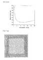
- FIG. 3is an exploded perspective view of the antenna circuit including a sheet metal allover the rear surface of the substrate;
- FIG. 4( a )shows a model of the antenna circuit used in a simulation for the aspect shown in FIG. 3 ;
- FIG. 4( b )is a distribution chart showing a current distribution as the result of simulation where using the model shown in FIG. 4( a );
- FIG. 4( c )shows a frequency characteristics as the result of simulation where using the model shown in FIG. 4( a );
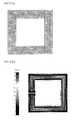
- FIG. 5is an exploded view showing an antenna circuit having a sheet metal on the rear surface area of the substrate opposing to the front surface area of the substrate having an antenna conductor;
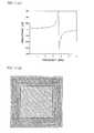
- FIG. 6( a )shows a model of the antenna circuit used in a simulation for the aspect shown in FIG. 5 ;
- FIG. 6( b )is a distribution chart showing a current distribution as the result of simulation where using the model shown in FIG. 6( a );
- FIG. 6( c )shows a frequency characteristics as the result of simulation where using the model shown in FIG. 6( a );
- FIG. 7( a )shows a model of the antenna circuit used in a simulation carried out for the antenna circuit comprising a notch-like slit in a part of a square-shaped sheet metal;
- FIG. 7( b )is a distribution chart showing the current distribution as the result of simulation where using the model shown in FIG. 7( a );
- FIG. 7( c )shows a frequency characteristics as the result of simulation where using the model shown in FIG. 7( a );
- FIG. 8is an exploded perspective view showing the antenna circuit having a sheet metal on only the rear surface area of the substrate opposed to the front surface area of the substrate having an antenna conductor, and having a slit of which the start end and terminal end are opened to the area at which the sheet metal does not exist;
- FIG. 9( a )shows a model of the antenna circuit used in the simulation for the aspect shown in FIG. 8 ;
- FIG. 9( b )is a distribution chart showing the current distribution as the result of simulation where using the model shown in FIG. 9( a );
- FIG. 9( c )shows a frequency characteristics as the result of simulation where using the model shown in FIG. 9( a );
- FIG. 10( a )shows a model of the antenna circuit used in the simulation carried out for the antenna circuit including the sheet metal divided in half, and a slit on the square-shaped sheet metal;
- FIG. 10( b )is a distribution chart showing the current distribution as the result of simulation where using the model shown in FIG. 10( a );
- FIG. 10( c )shows a frequency characteristics as the result of simulation where using the model shown in FIG. 10( a );
- FIG. 11( a )shows a model of the antenna circuit used in a simulation carried out for an antenna circuit wherein the sheet metal is divided into quarters, and a slit is provided on the square-shaped sheet metal;
- FIG. 11( b )is a distribution chart showing a current distribution as the result of simulation where using the model shown in FIG. 11( a );
- FIG. 11( c )shows a frequency characteristics as the result of simulation where using the model shown in FIG. 11( a );
- FIG. 12( a )shows a model of the antenna circuit used in a simulation carried out for the antenna circuit including a sheet metal having a square configuration in the inner periphery of the sheet metal having a loop configuration provided with a slit;
- FIG. 12( b )is a distribution chart showing the current distribution as the result of simulation where using the model shown in FIG. 12( a );
- FIG. 12( c )shows a frequency characteristics as the result of simulation where using the model shown in FIG. 12( a );
- FIG. 13( a )shows a model of the antenna circuit that was used in a simulation for the antenna circuit used a sheet metal having a loop configuration and the slits in the two parts;
- FIG. 13( b )is a distribution chart showing the current distribution as the result of simulation where using the model shown in FIG. 13( a );
- FIG. 13( c )shows a frequency characteristics as the result of simulation where using the model shown in FIG. 13( a );
- FIG. 14is a block diagram showing a basic circuit configuration of the transponder.
- this embodimentis for a transponder 10 serving as a non-contact IC (Integrated Circuit) card that reads/writes data without contact by radio communication with the predetermined reader/writer 1 , having a communication function, storing various readable and/or writable data, and being used in the RFID (Radio Frequency Identification) system.
- This transponder 10incorporates an antenna coil (loop antenna) having a so-called printed antenna, in which an antenna conductor is patterned and formed on a predetermined resin substrate as a matrix, and this transponder 10 has a resonant circuit formed by an extremely innovative method.
- the transponder 10is formed inside with a circuit board mounting at least an antenna coil and an IC chip.
- FIG. 2is a schematic perspective view showing a basic circuit board used in the transponder 10 .
- This circuit boardis formed by incorporating an IC chip integrating various members such as diode bridge, CPU (Central Processing Unit), ROM (Read Only Memory), and EEPROM (Electrically Erasable Programmable Read Only Memory) as a single semiconductor chip in order to realize a function of transponder for an antenna circuit 11 having at least an antenna conductor 13 formed with a predetermined conductor pattern forming the antenna coil on the surface of a predetermined substrate 12 in which the predetermined electrical conductor foil, such as copper foil, is provided on both sides of the predetermined insulating support.
- IC chipintegrating various members such as diode bridge, CPU (Central Processing Unit), ROM (Read Only Memory), and EEPROM (Electrically Erasable Programmable Read Only Memory) as a single semiconductor chip in order to realize a function of transponder for an antenna circuit 11 having at least an antenna conductor 13 formed with a predetermined conductor pattern forming the antenna coil
- the antenna circuit 11the main surface of the antenna circuit, for example, is formed in a rectangular shaped card.
- This antenna circuit 11can be formed with any kind of material if it is generally used as a substrate of the printed circuit board.
- the antenna circuit 11is formed with a so-called rigid substrate having the predetermined electrical conductor foil, such as a copper foil, formed on both sides, such as e.g., a paper phenol substrate defined as NEMA (National Electrical Manufacturers Association) grade XXP, XPC and the like, a paper polyester substrate defined as NEMA grade FR-2, a paper epoxy substrate defined as NEMA grade FR-3, a glass paper composite epoxy substrate defined as NEMA grade CEM-1, a glass unwoven paper composite epoxy substrate defined as NEMA grade CHE-3, a glass fabric epoxy substrate defined as NEMA grade G-10, and a glass fabric epoxy substrate defined as NEMA grade FR-4.
- the glass fabric epoxy substrate (FR-4)having less hygroscopicity, less change in size, and
- the antenna circuit 11is formed by the antenna conductor 13 as an emitting electrode, and the antenna conductor 13 is exposed and formed on the surface by photo-etching the electrical conductor foil of the one surface (hereinafter called the front surface) with respect to the electrical conductor foil disposed on each side of the substrate 12 .
- the spiral-shaped antenna conductor 13is formed on the front surface of the substrate 12 .
- FIG. 2shows a structure in which the spiral-shaped antenna conductor 13 is formed in winding patterns along each edge of the substrate 12 . Any antenna pattern by such antenna conductor 13 , however, can be used as long as it functions as an antenna coil. A spiral-shaped pattern wound in a substantially concentric fashion can be used.
- the inventor of the present applicationconceived utilizing an electrical conductor foil 14 disposed on the rear surface opposite to the front surface at which the antenna conductor 13 is formed, as a substitute structure for the conventional capacitors such as, e.g. an external type, an IC-equipped type, and film capacitor type, which form a conventional resonant circuit.
- the desired resonant conditionis not met when L-component of the antenna coil becomes small due to using a broad conductor pattern in order to reduce the conductor loss in the antenna coil.
- the inventor of the present applicationconsidered earning C-component as a solid pattern from the electrode in the rear surface of the substrate as much as possible in order to make up L-component.
- the forming method of the resonant circuitwhich the embodiment suggests is conceived from this kind of view, and forms the resonant circuit by a floating capacitance produced by a sheet metal on the rear surface and the antenna conductor on the front surface of the antenna circuit.
- an antenna circuit 21includes a sheet metal 24 on the rear surface of a substrate 22 as well as an antenna conductor 23 on the front surface side of the substrate 22 , wherein the substrate 22 is a double-sided board.
- the inventor of the present applicationcarried out a simulation for this kind of antenna circuit, and studied about the current distribution that flows in the sheet metal and the frequency characteristics. Specifically, the simulation was carried out using the square-shaped sheet metal as shown by a shaded area in FIG. 4( a ), and an antenna circuit having a spiral-shaped antenna conductor that is wound along each edge of the sheet metal as shown by a dashed line in FIG. 4( a ), as a model.
- the current distributionwas, as shown in FIG. 4( b ), that eddy current was generated allover the square-shaped sheet metal, and the frequency characteristics, as shown FIG. 4( c ), indicates grossly reduced inductance due to increased loss caused by eddy current flowing in the sheet metal as the frequency is increased.
- the inventor of the present applicationconceived an antenna circuit 31 .
- the antenna circuit 31includes a sheet metal 34 solely on the rear surface area of a substrate 32 opposed to the front surface area of the substrate 32 formed with an antenna conductor 33 .
- the antenna circuit 31is also formed with the antenna conductor 33 by manufacturing the front surface side of the sheet metal of the front surface side and rear surface side of the sheet metal provided on the substrate 32 having the double-sided board, such that the sheet metal is not provided allover the rear surface of the substrate 32 .
- the inventor of the present applicationconceived the antenna circuit 31 having a loop configuration in which a through hole 34 a is provided by cutting out a central part of the sheet metal for the sheet metal 34 .
- eddy currentcauses a trigger for deterioration of the characteristics. Consequently, to avoid eddy current by partially blocking the current flows on the sheet metal, a simulation was carried out using an antenna circuit comprising a notch-like slit in a part of a square-shaped sheet metal as a model, as shown by a shaded area in FIG. 7( a ).
- FIG. 7( b )shows, the current distribution of this time remains the same, that is only the current flows around the part of the slit, but eddy current still generates allover the sheet metal.
- FIG. 7( c )shows, the frequency characteristics do not satisfy the performance as an antenna coil although the inductance becomes larger compared to the result shown in FIG. 4( c ).
- an antenna circuit 41was configured by forming an antenna conductor 43 by manufacturing the front surface side of the sheet metal of the front surface side and rear surface sides of the sheet metal provided on a substrate 42 having double-sided board as shown by the exploded perspective view of FIG. 8 .
- a sheet metal 44 having a through hole 44 a provided by cutting out the central part of the sheet metalis disposed on the rear surface area of the substrate 42 , opposed to the front surface area of the substrate 42 having the antenna conductor 43 .
- a slit 44 b of which the start end A and the terminal end B are open to the area at which the sheet metal 44 does not exista structure in which the current does not loop allover the area at which the sheet metal is disposed is realized.
- the slit 44 bhas a configuration of which both of the start end A and the terminal end B are open to the area at which the sheet metal 44 does not exist.
- the reason why the slit has such a configurationis to eliminate a slit of which one end is closed by contacting the sheet metal such as a notch-like slit mentioned above, or a slit of which both ends are closed by drilling inside of the sheet metal.
- the currentflows along the sheet metal 44 having a loop configuration.
- the currentwill be blocked at the part of the slit 44 b and will not loop since the slit 44 b is disposed in order to disconnect a part of the loop configuration.
- the preferable antenna circuit 11 shown in FIG. 2 in the aboveis the antenna circuit comprising a sheet metal 14 on the rear surface area of the substrate 12 opposed to the area including the antenna conductor 13 on the front surface of the substrate 12 having a double-sided board and comprising a slit in a part of the sheet metal 14 preventing the current from looping allover the area including the sheet metal 14 .
- the antenna circuit 11thus can form a resonant circuit capable of having desired characteristics even though having a simple structure. Furthermore, this antenna circuit 11 can reduce the number of parts because an external type capacitor is not necessary as a capacitor for the resonant circuit, reducing the number of parts and thereby reducing the manufacturing cost. Moreover, it can reduce the area of the IC chip because it is not necessary to incorporate any capacitor in the IC chip, reducing the area of the IC chip eventually leads to preventing the manufacturing cost from increasing in this antenna circuit 11 .
- this antenna circuit 11does not need to electrically connect the front and rear sides of the double sided board through a through hole like the conventional film capacitors because the antenna conductor 13 formed on the front surface of the substrate 12 is solely connected with the IC chip, and it leads to reducing the cost of manufacturing.
- the antenna circuit 11can be easily manufactured since the antenna coil is formed as a printed antenna by using a reasonable printed circuit board as the substrate 12 .
- the total manufacturing costcan be significantly reduced because the antenna circuit 11 can be manufactured by using the manufacturing procedure of the printed circuit board.
- the embodimentis not limited to the embodiment mentioned above.
- a slitis provided in a part of the sheet metal having a loop configuration.
- the shape of the sheet metaldoes not matter if a slit of which the start end and terminal end are open to the area at which the sheet metal does not exist.
- FIG. 10( b ) and FIG. 10( c )show the result of the simulation where the sheet metal is divided in half.
- the current distributionwas that one of the current distributions of the sheet metal does not have an influence on the other current distribution though eddy current occurs in each sheet metal divided in half.
- the currentis blocked at a part of the slit, and the slit prevents the current from looping allover the area at which these two sheet metals are disposed.
- FIG. 10( c )shows, the level of frequency characteristics is good enough to function as an antenna coil with having a self resonance by the sheet metal effect, although the frequency characteristics is less deteriorated compared to the result shown in FIG. 9( c ).
- the square-shaped sheet metal divided into quarters by providing a slitcan be used as the antenna circuit.
- the current distributionindicates that one of the current distributions of the sheet metal does not have an influence on the other current distributions and the current is prevented from looping allover the area at which four sheet metals are disposed.
- the frequency characteristicsare improved compared to the result shown in FIG. 10( c ).
- a slitcan be provided in the sheet metal so as to divide the sheet metal into a plurality of sections.
- an antenna circuitcan be used in which the other sheet metal is disposed with a minute gap to be isolated electrically with the sheet metal on the inner periphery part of the loop-shaped sheet metal as well as disposing a sheet metal having a loop configuration provided with a slit.
- the current distributionindicates that the current is prevented from looping allover the area including two sheet metals having a loop configuration and a square configuration, although the current is induced at the edge of the square-shaped sheet metal disposed in the inner periphery.
- FIG. 12( b )shows that the current is prevented from looping allover the area including two sheet metals having a loop configuration and a square configuration, although the current is induced at the edge of the square-shaped sheet metal disposed in the inner periphery.
- FIG. 13( a ) to FIG. 13( c )show the result of the simulation where using the sheet metal having a loop configuration provided with two slits.
- FIG. 13( a )shows a model of the antenna circuit used in the simulation, and the model of the antenna circuit comprising the sheet metal having a loop configuration provided with the slits in two parts is shown by a shaded area in FIG. 13( a ).
- the spiral-shaped antenna conductor wound along each edge of the sheet metalis shown by a dashed line in FIG. 13( a ).
- the current distributionshows that the current is blocked at a part of the slit and prevents the current from looping allover the area at which the sheet metal is disposed as shown in FIG. 13( b ).
- the frequency characteristicsare improved, even though slightly, compared to the result shown in FIG. 9( c ).
- any configurations of the sheet metalcan be applied as long as it was provided with a slit of which both the start end and the terminal end are open to the area at which the sheet metal does not exist.
- reducing the area of the sheet metal and increasing the number of the slitsleads to decrease in the floating capacitance due to the decrease in the area of the sheet metal, although the entire loss of the current decreased. That is, there is a tradeoff relationship from the viewpoint of the characteristics. Therefore, in the antenna circuit, it is only necessary to change the configuration of the sheet metal or the number of the slits in accordance with the desired Q-value.
- the antenna coilwas formed as a printed-antenna, the present application is not limited to this, and anything can be applied as long as functioning as an antenna coil.
- transponder of the card typewas used for the explanation in the embodiment mentioned above, the present application can be applied to other various configurations on the basis of the usage, not limited to the card type.
Landscapes
- Engineering & Computer Science (AREA)
- Computer Hardware Design (AREA)
- Microelectronics & Electronic Packaging (AREA)
- Physics & Mathematics (AREA)
- General Physics & Mathematics (AREA)
- Theoretical Computer Science (AREA)
- Details Of Aerials (AREA)
- Near-Field Transmission Systems (AREA)
- Support Of Aerials (AREA)
Abstract
Description
Claims (7)
Applications Claiming Priority (3)
| Application Number | Priority Date | Filing Date | Title |
|---|---|---|---|
| JP2006-152032 | 2006-05-31 | ||
| JP2006152032AJP2007324865A (en) | 2006-05-31 | 2006-05-31 | Antenna circuit, and transponder |
| PCT/JP2007/054222WO2007138770A1 (en) | 2006-05-31 | 2007-03-05 | Antenna circuit and transponder |
Publications (2)
| Publication Number | Publication Date |
|---|---|
| US20090201116A1 US20090201116A1 (en) | 2009-08-13 |
| US8059062B2true US8059062B2 (en) | 2011-11-15 |
Family
ID=38778295
Family Applications (1)
| Application Number | Title | Priority Date | Filing Date |
|---|---|---|---|
| US12/302,471Expired - Fee RelatedUS8059062B2 (en) | 2006-05-31 | 2007-03-05 | Antenna circuit and transponder |
Country Status (5)
| Country | Link |
|---|---|
| US (1) | US8059062B2 (en) |
| JP (1) | JP2007324865A (en) |
| CN (2) | CN101536251A (en) |
| TW (1) | TWI474553B (en) |
| WO (1) | WO2007138770A1 (en) |
Cited By (3)
| Publication number | Priority date | Publication date | Assignee | Title |
|---|---|---|---|---|
| US20150236401A1 (en)* | 2012-09-06 | 2015-08-20 | Panasonic Intellectual Property Management Co., Ltd. | Antenna device and communications device |
| US20160043461A1 (en)* | 2014-01-30 | 2016-02-11 | Murata Manufacturing Co., Ltd. | Radio communication device |
| US20170194711A1 (en)* | 2014-05-30 | 2017-07-06 | Murata Manufacturing Co., Ltd. | Antenna device and electronic apparatus |
Families Citing this family (113)
| Publication number | Priority date | Publication date | Assignee | Title |
|---|---|---|---|---|
| US7519328B2 (en) | 2006-01-19 | 2009-04-14 | Murata Manufacturing Co., Ltd. | Wireless IC device and component for wireless IC device |
| US9064198B2 (en) | 2006-04-26 | 2015-06-23 | Murata Manufacturing Co., Ltd. | Electromagnetic-coupling-module-attached article |
| CN101467209B (en) | 2006-06-30 | 2012-03-21 | 株式会社村田制作所 | Optical disc |
| WO2008050535A1 (en) | 2006-09-26 | 2008-05-02 | Murata Manufacturing Co., Ltd. | Electromagnetically coupled module and article with electromagnetically coupled module |
| JP2008217522A (en)* | 2007-03-06 | 2008-09-18 | Nec Tokin Corp | Radio tag |
| US8235299B2 (en) | 2007-07-04 | 2012-08-07 | Murata Manufacturing Co., Ltd. | Wireless IC device and component for wireless IC device |
| EP2138962B1 (en) | 2007-04-26 | 2012-01-04 | Murata Manufacturing Co. Ltd. | Wireless ic device |
| EP2148449B1 (en) | 2007-05-11 | 2012-12-12 | Murata Manufacturing Co., Ltd. | Wireless ic device |
| EP2166617B1 (en) | 2007-07-09 | 2015-09-30 | Murata Manufacturing Co. Ltd. | Wireless ic device |
| EP2166490B1 (en) | 2007-07-17 | 2015-04-01 | Murata Manufacturing Co. Ltd. | Wireless ic device and electronic apparatus |
| CN102915462B (en) | 2007-07-18 | 2017-03-01 | 株式会社村田制作所 | Wireless IC device |
| ATE556466T1 (en)* | 2007-07-18 | 2012-05-15 | Murata Manufacturing Co | WIRELESS IC DEVICE |
| JP5174424B2 (en)* | 2007-10-24 | 2013-04-03 | デクセリアルズ株式会社 | Antenna circuit, resistance reduction method thereof, and transponder |
| JP4462388B2 (en) | 2007-12-20 | 2010-05-12 | 株式会社村田製作所 | Wireless IC device |
| CN103500875B (en) | 2007-12-26 | 2015-12-02 | 株式会社村田制作所 | Antenna assembly and Wireless IC device |
| EP2251934B1 (en) | 2008-03-03 | 2018-05-02 | Murata Manufacturing Co. Ltd. | Wireless ic device and wireless communication system |
| EP2284949B1 (en) | 2008-05-21 | 2016-08-03 | Murata Manufacturing Co. Ltd. | Wireless ic device |
| WO2009145007A1 (en) | 2008-05-26 | 2009-12-03 | 株式会社村田製作所 | Wireless ic device system and method for authenticating wireless ic device |
| KR101148534B1 (en) | 2008-05-28 | 2012-05-21 | 가부시키가이샤 무라타 세이사쿠쇼 | Wireless ic device and component for a wireless ic device |
| EP2320519B1 (en) | 2008-08-19 | 2017-04-12 | Murata Manufacturing Co., Ltd. | Wireless ic device and method for manufacturing same |
| JP5429182B2 (en)* | 2008-10-24 | 2014-02-26 | 株式会社村田製作所 | Wireless IC device |
| JP4525869B2 (en) | 2008-10-29 | 2010-08-18 | 株式会社村田製作所 | Wireless IC device |
| JP4605318B2 (en) | 2008-11-17 | 2011-01-05 | 株式会社村田製作所 | Antenna and wireless IC device |
| JP4934659B2 (en)* | 2008-11-26 | 2012-05-16 | 日本電信電話株式会社 | Shared antenna and matching circuit |
| CN103500873B (en) | 2009-01-09 | 2016-08-31 | 株式会社村田制作所 | Wireless ic device and wireless ic module |
| CN102204011B (en) | 2009-01-16 | 2013-12-25 | 株式会社村田制作所 | High frequency device and wireless IC device |
| EP2385580B1 (en) | 2009-01-30 | 2014-04-09 | Murata Manufacturing Co., Ltd. | Antenna and wireless ic device |
| JP5510450B2 (en) | 2009-04-14 | 2014-06-04 | 株式会社村田製作所 | Wireless IC device |
| EP2568534A3 (en) | 2009-04-21 | 2014-05-14 | Murata Manufacturing Co., Ltd. | Antenna devie and method of setting resonant frequency of antenna device |
| CN102449846B (en) | 2009-06-03 | 2015-02-04 | 株式会社村田制作所 | Wireless IC device and production method thereof |
| JP5516580B2 (en) | 2009-06-19 | 2014-06-11 | 株式会社村田製作所 | Wireless IC device and method for coupling power feeding circuit and radiation plate |
| JP5312587B2 (en)* | 2009-06-26 | 2013-10-09 | 三菱電機株式会社 | Wireless communication device |
| WO2010150403A1 (en) | 2009-06-26 | 2010-12-29 | 三菱電機株式会社 | Wireless communication device |
| WO2011001709A1 (en) | 2009-07-03 | 2011-01-06 | 株式会社村田製作所 | Antenna and antenna module |
| JP5182431B2 (en) | 2009-09-28 | 2013-04-17 | 株式会社村田製作所 | Wireless IC device and environmental state detection method using the same |
| JP5201270B2 (en) | 2009-09-30 | 2013-06-05 | 株式会社村田製作所 | Circuit board and manufacturing method thereof |
| JP5304580B2 (en) | 2009-10-02 | 2013-10-02 | 株式会社村田製作所 | Wireless IC device |
| CN102576939B (en) | 2009-10-16 | 2015-11-25 | 株式会社村田制作所 | Antenna and wireless ic device |
| JP5418600B2 (en) | 2009-10-27 | 2014-02-19 | 株式会社村田製作所 | Transceiver and RFID tag reader |
| JP5327334B2 (en) | 2009-11-04 | 2013-10-30 | 株式会社村田製作所 | Communication terminal and information processing system |
| WO2011055702A1 (en) | 2009-11-04 | 2011-05-12 | 株式会社村田製作所 | Wireless ic tag, reader/writer, and information processing system |
| WO2011055701A1 (en) | 2009-11-04 | 2011-05-12 | 株式会社村田製作所 | Communication terminal and information processing system |
| CN104617374B (en) | 2009-11-20 | 2018-04-06 | 株式会社村田制作所 | Mobile communication terminal |
| GB2488450B (en) | 2009-12-24 | 2014-08-20 | Murata Manufacturing Co | Antenna and mobile terminal |
| WO2011108340A1 (en) | 2010-03-03 | 2011-09-09 | 株式会社村田製作所 | Wireless communication module and wireless communication device |
| JP5403146B2 (en) | 2010-03-03 | 2014-01-29 | 株式会社村田製作所 | Wireless communication device and wireless communication terminal |
| CN102576940B (en) | 2010-03-12 | 2016-05-04 | 株式会社村田制作所 | Wireless communication devices and metal article processed |
| JP5370581B2 (en) | 2010-03-24 | 2013-12-18 | 株式会社村田製作所 | RFID system |
| WO2011122163A1 (en) | 2010-03-31 | 2011-10-06 | 株式会社村田製作所 | Antenna and wireless communication device |
| WO2011129151A1 (en)* | 2010-04-12 | 2011-10-20 | 株式会社村田製作所 | Antenna device and communication terminal device |
| JP5299351B2 (en) | 2010-05-14 | 2013-09-25 | 株式会社村田製作所 | Wireless IC device |
| JP5170156B2 (en) | 2010-05-14 | 2013-03-27 | 株式会社村田製作所 | Wireless IC device |
| JP5435130B2 (en)* | 2010-06-18 | 2014-03-05 | 株式会社村田製作所 | Communication terminal device and antenna device |
| WO2012005278A1 (en) | 2010-07-08 | 2012-01-12 | 株式会社村田製作所 | Antenna and rfid device |
| JP5723218B2 (en)* | 2010-07-13 | 2015-05-27 | キヤノン株式会社 | Loop antenna |
| GB2537773A (en) | 2010-07-28 | 2016-10-26 | Murata Manufacturing Co | Antenna apparatus and communication terminal instrument |
| JP5423897B2 (en) | 2010-08-10 | 2014-02-19 | 株式会社村田製作所 | Printed wiring board and wireless communication system |
| JP5234071B2 (en) | 2010-09-03 | 2013-07-10 | 株式会社村田製作所 | RFIC module |
| JP5630506B2 (en) | 2010-09-30 | 2014-11-26 | 株式会社村田製作所 | Wireless IC device |
| WO2012050037A1 (en) | 2010-10-12 | 2012-04-19 | 株式会社村田製作所 | Antenna apparatus and communication terminal apparatus |
| CN102971909B (en) | 2010-10-21 | 2014-10-15 | 株式会社村田制作所 | Communication terminal device |
| TWI460920B (en)* | 2010-10-25 | 2014-11-11 | Univ Nat Ilan | Anti-metal ultra high frequency radio frequency identification tag structure |
| WO2012093541A1 (en) | 2011-01-05 | 2012-07-12 | 株式会社村田製作所 | Wireless communication device |
| CN103299325B (en) | 2011-01-14 | 2016-03-02 | 株式会社村田制作所 | RFID chip packaging and RFID tags |
| CN103119786B (en) | 2011-02-28 | 2015-07-22 | 株式会社村田制作所 | Wireless communication device |
| WO2012121185A1 (en) | 2011-03-08 | 2012-09-13 | 株式会社村田製作所 | Antenna device and communication terminal apparatus |
| WO2012137717A1 (en) | 2011-04-05 | 2012-10-11 | 株式会社村田製作所 | Wireless communication device |
| WO2012141070A1 (en) | 2011-04-13 | 2012-10-18 | 株式会社村田製作所 | Wireless ic device and wireless communication terminal |
| FR2974259B1 (en)* | 2011-04-18 | 2013-06-07 | Commissariat Energie Atomique | RECEIVER POWERED BY AN INDUCTIVE TYPE WIRELESS INTERFACE |
| WO2012157596A1 (en) | 2011-05-16 | 2012-11-22 | 株式会社村田製作所 | Wireless ic device |
| CN102810725B (en)* | 2011-05-31 | 2016-05-04 | 比亚迪股份有限公司 | A near field communication antenna |
| KR101338173B1 (en) | 2011-07-14 | 2013-12-06 | 가부시키가이샤 무라타 세이사쿠쇼 | Wireless communication device |
| WO2013011856A1 (en) | 2011-07-15 | 2013-01-24 | 株式会社村田製作所 | Wireless communication device |
| CN204189963U (en) | 2011-07-19 | 2015-03-04 | 株式会社村田制作所 | Antenna assembly and communication terminal |
| EP2562868A1 (en)* | 2011-08-22 | 2013-02-27 | Laird Technologies AB | A multiple-turn loop antenna arrangement and a portable radio communication device comprising such an arrangement |
| WO2013035821A1 (en) | 2011-09-09 | 2013-03-14 | 株式会社村田製作所 | Antenna device and wireless device |
| JP5344108B1 (en) | 2011-12-01 | 2013-11-20 | 株式会社村田製作所 | Wireless IC device and manufacturing method thereof |
| EP2688145A1 (en) | 2012-01-30 | 2014-01-22 | Murata Manufacturing Co., Ltd. | Wireless ic device |
| WO2013115017A1 (en)* | 2012-02-02 | 2013-08-08 | 株式会社村田製作所 | Antenna device |
| JP5464307B2 (en) | 2012-02-24 | 2014-04-09 | 株式会社村田製作所 | ANTENNA DEVICE AND WIRELESS COMMUNICATION DEVICE |
| CN104487985B (en) | 2012-04-13 | 2020-06-26 | 株式会社村田制作所 | RFID tag inspection method and inspection device |
| US9083073B2 (en)* | 2012-06-28 | 2015-07-14 | Intel Corporation | Thin chassis near field communication (NFC) antenna integration |
| JP6112383B2 (en)* | 2012-06-28 | 2017-04-12 | パナソニックIpマネジメント株式会社 | Mobile device |
| JP2014175586A (en)* | 2013-03-12 | 2014-09-22 | Nippon Soken Inc | Magnetic field resonance coil device |
| US11354558B2 (en) | 2013-01-18 | 2022-06-07 | Amatech Group Limited | Contactless smartcards with coupling frames |
| EP2838157A1 (en) | 2013-08-14 | 2015-02-18 | Samsung Electro-Mechanics Co., Ltd. | Cover for electronic device, antenna assembly, electronic device, and method for manufacturing the same |
| WO2015108054A1 (en)* | 2014-01-17 | 2015-07-23 | デクセリアルズ株式会社 | Antenna device and electronic apparatus |
| US10186753B2 (en)* | 2014-01-31 | 2019-01-22 | Tdk Corporation | Antenna device and portable electronic device using the same |
| JP2015211421A (en)* | 2014-04-30 | 2015-11-24 | Tdk株式会社 | Antenna device |
| US10290934B2 (en)* | 2014-04-30 | 2019-05-14 | Tdk Corporation | Antenna device |
| JP6318826B2 (en)* | 2014-04-30 | 2018-05-09 | Tdk株式会社 | Antenna device |
| CN105990679B (en)* | 2015-02-13 | 2019-03-05 | 鸿富锦精密工业(深圳)有限公司 | Electronic device |
| JP2016178527A (en)* | 2015-03-20 | 2016-10-06 | Tdk株式会社 | Antenna device |
| WO2016160359A1 (en)* | 2015-04-01 | 2016-10-06 | 3M Innovative Properties Company | Radio frequency identification tag |
| CN105631381A (en)* | 2016-03-25 | 2016-06-01 | 福建师范大学 | Electronic tag reader with antenna signal directional enhancing function |
| US10886598B2 (en)* | 2016-11-16 | 2021-01-05 | Wits Co., Ltd. | Antenna module and electronic device having the same |
| CN107546470A (en)* | 2017-07-18 | 2018-01-05 | 苏州佳世达电通有限公司 | Communication device |
| WO2019144054A1 (en)* | 2018-01-19 | 2019-07-25 | Johnson Controls Technology Company | Hand hygiene and surgical scrub system |
| TWI816134B (en)* | 2021-06-09 | 2023-09-21 | 財團法人工業技術研究院 | Antenna module |
| US20230145030A1 (en)* | 2021-11-03 | 2023-05-11 | Nucurrent, Inc. | Wireless Power Transmitter with Metal Mesh for Resiliency |
| US11831175B2 (en) | 2021-11-03 | 2023-11-28 | Nucurrent, Inc. | Wireless power transmission antenna with antenna molecules |
| US11848566B2 (en) | 2021-11-03 | 2023-12-19 | Nucurrent, Inc. | Dual communications demodulation of a wireless power transmission system having an internal repeater |
| US11831176B2 (en) | 2021-11-03 | 2023-11-28 | Nucurrent, Inc. | Wireless power transfer systems with substantial uniformity over a large area |
| US11862984B2 (en) | 2021-11-03 | 2024-01-02 | Nucurrent, Inc. | Wireless power receiver with repeater for enhanced power harvesting |
| US11831177B2 (en) | 2021-11-03 | 2023-11-28 | Nucurrent, Inc. | Wireless power transmitter with internal repeater and enhanced uniformity |
| US11962337B2 (en) | 2021-11-03 | 2024-04-16 | Nucurrent, Inc. | Communications demodulation in wireless power transmission system having an internal repeater |
| US12027880B2 (en) | 2021-11-03 | 2024-07-02 | Nucurrent, Inc. | Wireless power transfer from mouse pad to mouse |
| US11824372B2 (en) | 2021-11-03 | 2023-11-21 | Nucurrent, Inc. | Wireless power transmission antenna with puzzled antenna molecules |
| US11824373B2 (en) | 2021-11-03 | 2023-11-21 | Nucurrent, Inc. | Wireless power transmission antenna with parallel coil molecule configuration |
| US11824371B2 (en) | 2021-11-03 | 2023-11-21 | Nucurrent, Inc. | Wireless power transmission antenna with internal repeater and repeater filter |
| US11862991B2 (en) | 2021-11-03 | 2024-01-02 | Nucurrent, Inc. | Wireless power transmission antenna with internal repeater and in-coil tuning |
| US11831173B2 (en) | 2021-11-03 | 2023-11-28 | Nucurrent, Inc. | Wireless power transmission antenna with series coil molecule configuration |
| KR102783843B1 (en)* | 2021-11-22 | 2025-03-21 | 코나엠 주식회사 | A metal ic card and a method for producing the metal ic card |
Citations (28)
| Publication number | Priority date | Publication date | Assignee | Title |
|---|---|---|---|---|
| JPH04101168A (en) | 1990-08-21 | 1992-04-02 | Brother Ind Ltd | Image forming device |
| JPH0810160A (en) | 1994-06-28 | 1996-01-16 | Tokyo Gas Co Ltd | Food steamer |
| JPH08330839A (en) | 1995-05-29 | 1996-12-13 | Sony Chem Corp | Antenna for short-range communication and its utilization |
| JPH09139698A (en) | 1995-11-15 | 1997-05-27 | Matsushita Electric Works Ltd | Data carrier for mobile body identification device |
| JPH11238103A (en) | 1997-12-18 | 1999-08-31 | Denso Corp | Non-contact ic card reader-writer |
| JP2000505923A (en) | 1996-12-20 | 2000-05-16 | シーメンス アクチエンゲゼルシヤフト | Non-conductive substrate forming a strip or panel on which multiple carrier elements are formed |
| JP2000196339A (en) | 1998-12-24 | 2000-07-14 | Sony Corp | Antenna system and electronic device having the same and electronic equipment |
| JP2000278027A (en) | 1999-03-25 | 2000-10-06 | Sony Corp | Antenna for small-sized dielectric tag |
| US6181287B1 (en)* | 1997-03-10 | 2001-01-30 | Precision Dynamics Corporation | Reactively coupled elements in circuits on flexible substrates |
| JP2003157420A (en) | 2002-07-03 | 2003-05-30 | Hitachi Chem Co Ltd | Ic tag |
| JP2003215271A (en) | 2002-01-18 | 2003-07-30 | Seiko Epson Corp | Electronic watch |
| JP2003331250A (en) | 2002-03-05 | 2003-11-21 | Mitsubishi Materials Corp | Small disk with rfid |
| US20040074974A1 (en)* | 2000-07-19 | 2004-04-22 | Fujio Senba | Rfid tag housing structure, rfid tag installation structure and rfid tag communication method |
| US20050007296A1 (en)* | 2001-09-28 | 2005-01-13 | Takanori Endo | Antenna coil and rfid-use tag using it, transponder-use antenna |
| WO2005004047A1 (en) | 2003-07-03 | 2005-01-13 | Renesas Technology Corp. | Multi-function card device |
| JP2005067585A (en) | 2003-08-07 | 2005-03-17 | Mitsubishi Materials Corp | Tire state measuring rfid system, antenna of tag and wheel equipped with antenna |
| JP2005080023A (en) | 2003-09-01 | 2005-03-24 | Sony Corp | Magnetic core member, antenna module and portable communication terminal provided with the same |
| JP2005109603A (en) | 2003-09-29 | 2005-04-21 | Citizen Watch Co Ltd | Portable electronic apparatus provided with contactless data communication function |
| JP2005170389A (en) | 2003-12-08 | 2005-06-30 | Mitsubishi Materials Corp | Metallic container with rfid tag |
| JP2006060432A (en) | 2004-08-18 | 2006-03-02 | Mitsui Chemicals Inc | Radio wave transmitting and receiving antenna |
| US20060266435A1 (en)* | 2005-04-26 | 2006-11-30 | Yang Jae S | Magnetic sheet for radio frequency identification antenna, method of manufacturing the same, and radio frequency identification antenna using the same |
| US7209281B2 (en)* | 2004-04-28 | 2007-04-24 | Seiko Epson Corporation | Electrophoretic display device and contactless communication medium |
| US20070252706A1 (en)* | 2005-01-11 | 2007-11-01 | Fujitsu Limited | IC tag housing case |
| US20080003457A1 (en)* | 2004-02-13 | 2008-01-03 | Mitsubishi Materials Corporation | High-frequency magnetic core material, its manufacturing method, and antenna including the magnetic core material |
| US20080129629A1 (en)* | 2005-07-07 | 2008-06-05 | Toda Kogyo Corporation | Magnetic antenna and board mounted with the same |
| JP4101168B2 (en) | 2003-12-24 | 2008-06-18 | 古河電気工業株式会社 | Power supply device for sliding door |
| US20090146898A1 (en)* | 2004-04-27 | 2009-06-11 | Sony Corporation | Antenna Module-Use Magnetic Core Member, Antenna Module, and Portable Information Terminal Having the Same |
| US7652579B2 (en)* | 2004-07-08 | 2010-01-26 | Ykk Corporation | Article with wireless IC tag |
Family Cites Families (6)
| Publication number | Priority date | Publication date | Assignee | Title |
|---|---|---|---|---|
| JP2558330Y2 (en)* | 1991-02-06 | 1997-12-24 | オムロン株式会社 | Electromagnetic coupling type electronic equipment |
| FR2787640B1 (en)* | 1998-12-22 | 2003-02-14 | Gemplus Card Int | ARRANGEMENT OF AN ANTENNA IN A METALLIC ENVIRONMENT |
| US6897830B2 (en)* | 2002-07-04 | 2005-05-24 | Antenna Tech, Inc. | Multi-band helical antenna |
| US7268687B2 (en)* | 2004-03-23 | 2007-09-11 | 3M Innovative Properties Company | Radio frequency identification tags with compensating elements |
| JP2006050265A (en)* | 2004-08-04 | 2006-02-16 | Sony Corp | Magnetic core member for antenna module, antenna module and personal digital assistant provided therewith |
| JP4747294B2 (en)* | 2005-05-26 | 2011-08-17 | 三菱マテリアル株式会社 | RFID tag |
- 2006
- 2006-05-31JPJP2006152032Apatent/JP2007324865A/enactivePending
- 2007
- 2007-03-05USUS12/302,471patent/US8059062B2/ennot_activeExpired - Fee Related
- 2007-03-05CNCNA2007800199263Apatent/CN101536251A/enactivePending
- 2007-03-05WOPCT/JP2007/054222patent/WO2007138770A1/enactiveSearch and Examination
- 2007-03-05CNCN201410680955.6Apatent/CN104377425A/enactivePending
- 2007-03-12TWTW96108469Apatent/TWI474553B/ennot_activeIP Right Cessation
Patent Citations (29)
| Publication number | Priority date | Publication date | Assignee | Title |
|---|---|---|---|---|
| JPH04101168A (en) | 1990-08-21 | 1992-04-02 | Brother Ind Ltd | Image forming device |
| JPH0810160A (en) | 1994-06-28 | 1996-01-16 | Tokyo Gas Co Ltd | Food steamer |
| JPH08330839A (en) | 1995-05-29 | 1996-12-13 | Sony Chem Corp | Antenna for short-range communication and its utilization |
| JPH09139698A (en) | 1995-11-15 | 1997-05-27 | Matsushita Electric Works Ltd | Data carrier for mobile body identification device |
| JP2000505923A (en) | 1996-12-20 | 2000-05-16 | シーメンス アクチエンゲゼルシヤフト | Non-conductive substrate forming a strip or panel on which multiple carrier elements are formed |
| US6181287B1 (en)* | 1997-03-10 | 2001-01-30 | Precision Dynamics Corporation | Reactively coupled elements in circuits on flexible substrates |
| JPH11238103A (en) | 1997-12-18 | 1999-08-31 | Denso Corp | Non-contact ic card reader-writer |
| JP2000196339A (en) | 1998-12-24 | 2000-07-14 | Sony Corp | Antenna system and electronic device having the same and electronic equipment |
| JP2000278027A (en) | 1999-03-25 | 2000-10-06 | Sony Corp | Antenna for small-sized dielectric tag |
| US20040074974A1 (en)* | 2000-07-19 | 2004-04-22 | Fujio Senba | Rfid tag housing structure, rfid tag installation structure and rfid tag communication method |
| US20050007296A1 (en)* | 2001-09-28 | 2005-01-13 | Takanori Endo | Antenna coil and rfid-use tag using it, transponder-use antenna |
| JP2003215271A (en) | 2002-01-18 | 2003-07-30 | Seiko Epson Corp | Electronic watch |
| JP2003331250A (en) | 2002-03-05 | 2003-11-21 | Mitsubishi Materials Corp | Small disk with rfid |
| JP2003157420A (en) | 2002-07-03 | 2003-05-30 | Hitachi Chem Co Ltd | Ic tag |
| WO2005004047A1 (en) | 2003-07-03 | 2005-01-13 | Renesas Technology Corp. | Multi-function card device |
| JP2005067585A (en) | 2003-08-07 | 2005-03-17 | Mitsubishi Materials Corp | Tire state measuring rfid system, antenna of tag and wheel equipped with antenna |
| JP2005080023A (en) | 2003-09-01 | 2005-03-24 | Sony Corp | Magnetic core member, antenna module and portable communication terminal provided with the same |
| JP2005109603A (en) | 2003-09-29 | 2005-04-21 | Citizen Watch Co Ltd | Portable electronic apparatus provided with contactless data communication function |
| JP2005170389A (en) | 2003-12-08 | 2005-06-30 | Mitsubishi Materials Corp | Metallic container with rfid tag |
| JP4101168B2 (en) | 2003-12-24 | 2008-06-18 | 古河電気工業株式会社 | Power supply device for sliding door |
| US20080003457A1 (en)* | 2004-02-13 | 2008-01-03 | Mitsubishi Materials Corporation | High-frequency magnetic core material, its manufacturing method, and antenna including the magnetic core material |
| US20090146898A1 (en)* | 2004-04-27 | 2009-06-11 | Sony Corporation | Antenna Module-Use Magnetic Core Member, Antenna Module, and Portable Information Terminal Having the Same |
| US7209281B2 (en)* | 2004-04-28 | 2007-04-24 | Seiko Epson Corporation | Electrophoretic display device and contactless communication medium |
| US7652579B2 (en)* | 2004-07-08 | 2010-01-26 | Ykk Corporation | Article with wireless IC tag |
| JP2006060432A (en) | 2004-08-18 | 2006-03-02 | Mitsui Chemicals Inc | Radio wave transmitting and receiving antenna |
| US20070252706A1 (en)* | 2005-01-11 | 2007-11-01 | Fujitsu Limited | IC tag housing case |
| US20060266435A1 (en)* | 2005-04-26 | 2006-11-30 | Yang Jae S | Magnetic sheet for radio frequency identification antenna, method of manufacturing the same, and radio frequency identification antenna using the same |
| US20100288418A1 (en)* | 2005-04-26 | 2010-11-18 | Amotech Co., Ltd. | Magnetic sheet for radio frequency identification antenna, method of manufacturing the same, and radio frequency identification antenna using the same |
| US20080129629A1 (en)* | 2005-07-07 | 2008-06-05 | Toda Kogyo Corporation | Magnetic antenna and board mounted with the same |
Cited By (8)
| Publication number | Priority date | Publication date | Assignee | Title |
|---|---|---|---|---|
| US20150236401A1 (en)* | 2012-09-06 | 2015-08-20 | Panasonic Intellectual Property Management Co., Ltd. | Antenna device and communications device |
| US10224601B2 (en)* | 2012-09-06 | 2019-03-05 | Panasonic Intelletual Property Management Co., Ltd. | Antenna device and communications device |
| US10396439B2 (en) | 2012-09-06 | 2019-08-27 | Panasonic Intellectual Property Management Co., Ltd. | Antenna device and communications device |
| US10658734B2 (en)* | 2012-09-06 | 2020-05-19 | Panasonic Intellectual Property Management Co., Ltd. | Antenna device and communications device |
| US20160043461A1 (en)* | 2014-01-30 | 2016-02-11 | Murata Manufacturing Co., Ltd. | Radio communication device |
| US9947991B2 (en)* | 2014-01-30 | 2018-04-17 | Murata Manufacturing Co., Ltd. | Radio communication device |
| US20170194711A1 (en)* | 2014-05-30 | 2017-07-06 | Murata Manufacturing Co., Ltd. | Antenna device and electronic apparatus |
| US10164336B2 (en)* | 2014-05-30 | 2018-12-25 | Murata Manufacturing Co., Ltd. | Antenna device and electronic apparatus |
Also Published As
| Publication number | Publication date |
|---|---|
| JP2007324865A (en) | 2007-12-13 |
| US20090201116A1 (en) | 2009-08-13 |
| CN104377425A (en) | 2015-02-25 |
| CN101536251A (en) | 2009-09-16 |
| TWI474553B (en) | 2015-02-21 |
| WO2007138770A1 (en) | 2007-12-06 |
| TW200744253A (en) | 2007-12-01 |
Similar Documents
| Publication | Publication Date | Title |
|---|---|---|
| US8059062B2 (en) | Antenna circuit and transponder | |
| US9016592B2 (en) | Antenna device and communication terminal apparatus | |
| US7323977B2 (en) | Tunable RFID tag for global applications | |
| JP5429182B2 (en) | Wireless IC device | |
| US8297516B2 (en) | Coil antenna and non-contact information medium | |
| US9104954B2 (en) | Radiofrequency transponder device with optimized passive resonant circuit | |
| US7800503B2 (en) | Radio frequency identification (RFID) tag antenna design | |
| US8665167B2 (en) | Antenna circuit, method for reducing resistance of antenna circuit, and transponder | |
| CN106339746B (en) | Multi-frequency transponder with single antenna | |
| JP5026522B2 (en) | Optimized reading method and system for transponders for high frequency communications using passive resonant circuits | |
| US20090033580A1 (en) | RFID Antenna | |
| US20090309703A1 (en) | Rfid device with conductive loop shield | |
| US9252493B2 (en) | Wire capacitor, in particular for a radio frequency circuit, and device comprising said wire capacitor | |
| US9852369B2 (en) | Electronic entity having an RFID transponder | |
| KR20140047603A (en) | Small broadband loop antenna for near field applications | |
| JP2006262055A (en) | Antenna module and portable information terminal provided with the same | |
| JP2005033587A (en) | Antenna circuit and noncontact ic card | |
| JP5108131B2 (en) | Antenna circuit and transponder | |
| US8890749B2 (en) | Transceiver device | |
| KR100862477B1 (en) | RFID tag | |
| JP6590119B1 (en) | RFID tag and article with RFID | |
| KR20090113947A (en) | RDF Tag Coil Antenna |
Legal Events
| Date | Code | Title | Description |
|---|---|---|---|
| AS | Assignment | Owner name:SONY CHEMICAL & INFORMATION DEVICE CORPORATION, JA Free format text:ASSIGNMENT OF ASSIGNORS INTEREST;ASSIGNOR:ORIHARA, KATSUHISA;REEL/FRAME:021925/0951 Effective date:20081120 | |
| AS | Assignment | Owner name:SONY CHEMICAL & INFORMATION DEVICE CORPORATION, JA Free format text:ASSIGNMENT OF ASSIGNORS INTEREST;ASSIGNOR:SONY CHEMICAL & INFORMATION DEVICE CORPORATION;REEL/FRAME:026846/0721 Effective date:20110824 Owner name:SONY CORPORATION, JAPAN Free format text:ASSIGNMENT OF ASSIGNORS INTEREST;ASSIGNOR:SONY CHEMICAL & INFORMATION DEVICE CORPORATION;REEL/FRAME:026846/0721 Effective date:20110824 | |
| STCF | Information on status: patent grant | Free format text:PATENTED CASE | |
| AS | Assignment | Owner name:DEXERIALS CORPORATION, JAPAN Free format text:CHANGE OF NAME;ASSIGNOR:SONY CHEMICAL & INFORMATION DEVICE CORPORATION;REEL/FRAME:029908/0665 Effective date:20120928 | |
| FPAY | Fee payment | Year of fee payment:4 | |
| FEPP | Fee payment procedure | Free format text:MAINTENANCE FEE REMINDER MAILED (ORIGINAL EVENT CODE: REM.); ENTITY STATUS OF PATENT OWNER: LARGE ENTITY | |
| LAPS | Lapse for failure to pay maintenance fees | Free format text:PATENT EXPIRED FOR FAILURE TO PAY MAINTENANCE FEES (ORIGINAL EVENT CODE: EXP.); ENTITY STATUS OF PATENT OWNER: LARGE ENTITY | |
| STCH | Information on status: patent discontinuation | Free format text:PATENT EXPIRED DUE TO NONPAYMENT OF MAINTENANCE FEES UNDER 37 CFR 1.362 | |
| FP | Lapsed due to failure to pay maintenance fee | Effective date:20191115 |