US8058659B2 - LED chip-based lighting products and methods of building - Google Patents
LED chip-based lighting products and methods of buildingDownload PDFInfo
- Publication number
- US8058659B2 US8058659B2US12/857,472US85747210AUS8058659B2US 8058659 B2US8058659 B2US 8058659B2US 85747210 AUS85747210 AUS 85747210AUS 8058659 B2US8058659 B2US 8058659B2
- Authority
- US
- United States
- Prior art keywords
- conductors
- led chips
- led
- lighting product
- cover plate
- Prior art date
- Legal status (The legal status is an assumption and is not a legal conclusion. Google has not performed a legal analysis and makes no representation as to the accuracy of the status listed.)
- Active
Links
Images


Classifications
- H—ELECTRICITY
- H10—SEMICONDUCTOR DEVICES; ELECTRIC SOLID-STATE DEVICES NOT OTHERWISE PROVIDED FOR
- H10H—INORGANIC LIGHT-EMITTING SEMICONDUCTOR DEVICES HAVING POTENTIAL BARRIERS
- H10H20/00—Individual inorganic light-emitting semiconductor devices having potential barriers, e.g. light-emitting diodes [LED]
- H10H20/80—Constructional details
- H10H20/85—Packages
- H10H20/855—Optical field-shaping means, e.g. lenses
- H10H20/856—Reflecting means
- H—ELECTRICITY
- H10—SEMICONDUCTOR DEVICES; ELECTRIC SOLID-STATE DEVICES NOT OTHERWISE PROVIDED FOR
- H10H—INORGANIC LIGHT-EMITTING SEMICONDUCTOR DEVICES HAVING POTENTIAL BARRIERS
- H10H20/00—Individual inorganic light-emitting semiconductor devices having potential barriers, e.g. light-emitting diodes [LED]
- H10H20/80—Constructional details
- H10H20/85—Packages
- H10H20/855—Optical field-shaping means, e.g. lenses
- H—ELECTRICITY
- H10—SEMICONDUCTOR DEVICES; ELECTRIC SOLID-STATE DEVICES NOT OTHERWISE PROVIDED FOR
- H10H—INORGANIC LIGHT-EMITTING SEMICONDUCTOR DEVICES HAVING POTENTIAL BARRIERS
- H10H20/00—Individual inorganic light-emitting semiconductor devices having potential barriers, e.g. light-emitting diodes [LED]
- H10H20/80—Constructional details
- H10H20/85—Packages
- H10H20/857—Interconnections, e.g. lead-frames, bond wires or solder balls
- H—ELECTRICITY
- H01—ELECTRIC ELEMENTS
- H01L—SEMICONDUCTOR DEVICES NOT COVERED BY CLASS H10
- H01L25/00—Assemblies consisting of a plurality of semiconductor or other solid state devices
- H01L25/03—Assemblies consisting of a plurality of semiconductor or other solid state devices all the devices being of a type provided for in a single subclass of subclasses H10B, H10D, H10F, H10H, H10K or H10N, e.g. assemblies of rectifier diodes
- H01L25/04—Assemblies consisting of a plurality of semiconductor or other solid state devices all the devices being of a type provided for in a single subclass of subclasses H10B, H10D, H10F, H10H, H10K or H10N, e.g. assemblies of rectifier diodes the devices not having separate containers
- H01L25/075—Assemblies consisting of a plurality of semiconductor or other solid state devices all the devices being of a type provided for in a single subclass of subclasses H10B, H10D, H10F, H10H, H10K or H10N, e.g. assemblies of rectifier diodes the devices not having separate containers the devices being of a type provided for in group H10H20/00
- H01L25/0753—Assemblies consisting of a plurality of semiconductor or other solid state devices all the devices being of a type provided for in a single subclass of subclasses H10B, H10D, H10F, H10H, H10K or H10N, e.g. assemblies of rectifier diodes the devices not having separate containers the devices being of a type provided for in group H10H20/00 the devices being arranged next to each other
- H—ELECTRICITY
- H01—ELECTRIC ELEMENTS
- H01L—SEMICONDUCTOR DEVICES NOT COVERED BY CLASS H10
- H01L2924/00—Indexing scheme for arrangements or methods for connecting or disconnecting semiconductor or solid-state bodies as covered by H01L24/00
- H01L2924/0001—Technical content checked by a classifier
- H01L2924/0002—Not covered by any one of groups H01L24/00, H01L24/00 and H01L2224/00
- H—ELECTRICITY
- H05—ELECTRIC TECHNIQUES NOT OTHERWISE PROVIDED FOR
- H05K—PRINTED CIRCUITS; CASINGS OR CONSTRUCTIONAL DETAILS OF ELECTRIC APPARATUS; MANUFACTURE OF ASSEMBLAGES OF ELECTRICAL COMPONENTS
- H05K1/00—Printed circuits
- H05K1/02—Details
- H05K1/03—Use of materials for the substrate
- H05K1/05—Insulated conductive substrates, e.g. insulated metal substrate
- H05K1/056—Insulated conductive substrates, e.g. insulated metal substrate the metal substrate being covered by an organic insulating layer
- H—ELECTRICITY
- H10—SEMICONDUCTOR DEVICES; ELECTRIC SOLID-STATE DEVICES NOT OTHERWISE PROVIDED FOR
- H10H—INORGANIC LIGHT-EMITTING SEMICONDUCTOR DEVICES HAVING POTENTIAL BARRIERS
- H10H20/00—Individual inorganic light-emitting semiconductor devices having potential barriers, e.g. light-emitting diodes [LED]
- H10H20/01—Manufacture or treatment
- H10H20/036—Manufacture or treatment of packages
- H—ELECTRICITY
- H10—SEMICONDUCTOR DEVICES; ELECTRIC SOLID-STATE DEVICES NOT OTHERWISE PROVIDED FOR
- H10H—INORGANIC LIGHT-EMITTING SEMICONDUCTOR DEVICES HAVING POTENTIAL BARRIERS
- H10H20/00—Individual inorganic light-emitting semiconductor devices having potential barriers, e.g. light-emitting diodes [LED]
- H10H20/80—Constructional details
- H10H20/85—Packages
- H10H20/852—Encapsulations
- H10H20/853—Encapsulations characterised by their shape
- Y—GENERAL TAGGING OF NEW TECHNOLOGICAL DEVELOPMENTS; GENERAL TAGGING OF CROSS-SECTIONAL TECHNOLOGIES SPANNING OVER SEVERAL SECTIONS OF THE IPC; TECHNICAL SUBJECTS COVERED BY FORMER USPC CROSS-REFERENCE ART COLLECTIONS [XRACs] AND DIGESTS
- Y10—TECHNICAL SUBJECTS COVERED BY FORMER USPC
- Y10T—TECHNICAL SUBJECTS COVERED BY FORMER US CLASSIFICATION
- Y10T29/00—Metal working
- Y10T29/49—Method of mechanical manufacture
- Y10T29/49002—Electrical device making
- Y10T29/49117—Conductor or circuit manufacturing
- Y10T29/49124—On flat or curved insulated base, e.g., printed circuit, etc.
- Y10T29/4913—Assembling to base an electrical component, e.g., capacitor, etc.
Definitions
- LEDLight-emitting diode
- Solid-state LEDsare generally manufactured and packaged like other semiconductor products; that is, the LEDs are first fabricated in wafer form, then wafers are diced into individual LED chips that are assembled into individual packages. The packages then mount into products in a variety of ways. In this way, packaging cost is incurred for each individual LED, with this cost accumulating in each product that uses the LEDs.
- Net brightness from a single point sourceis also an issue with LED based lighting.
- the current trend in solid-state lightingis to employ large LED chips and/or modules of LED chips that have been incorporated onto a printed circuit board (PCB) assembly.
- PCBprinted circuit board
- Management of manufacturing costscurrently favors use of large LED chips (e.g., packaged chips that consume about one watt of electrical power and emit about 80 to 300 lumens of light) because lower numbers of chips and packages are used in a final product.
- large LED chipse.g., packaged chips that consume about one watt of electrical power and emit about 80 to 300 lumens of light
- userssometimes find the large LED chips uncomfortably bright.
- placement of large LED chips into a light fixture in an arrayed fashionmay result in the fixture projecting a distracting distribution of light.
- Managing heat transfer away from large LED chips and/or the PCB assembliesmay also be problematic.
- a method of building a light-emitting diode (LED) chip-based lighting productincludes patterning conductors on an inside surface of a panel, mounting a plurality of unpackaged LED chips directly on the conductors, and integrating the panel with support structure to form the lighting product such that an outside surface of the panel forms an exterior surface of the lighting product.
- LEDlight-emitting diode
- a light-emitting diode (LED) chip-based lighting productincludes a panel having an inner surface and an outer surface, the outer surface forming an external surface of the lighting product, conductors patterned on the inner surface, and a plurality of unpackaged LED chips mounted directly to the conductors.
- LEDlight-emitting diode
- a light emitting diode (LED)-based lighting productincludes a panel having an inner surface and an outer surface, the outer surface forming an external surface of the lighting product, conductors patterned on the inner surface, and a plurality of LEDs mounted directly to the conductors.
- LEDlight emitting diode
- FIG. 1shows an LED-based lighting product, in accord with an embodiment.
- FIG. 2shows a printed circuit board (“PCB”) assembly with LED chips assembled thereon, in accord with an embodiment.
- PCBprinted circuit board
- FIG. 3illustrates an early stage of fabrication of a PCB, in accord with an embodiment.
- FIG. 4illustrates components mounted to the PCB of FIG. 3 , in accord with an embodiment.
- FIG. 5Ais a side view of a cover plate with conductors, in accord with an embodiment.
- FIG. 5Bis a side view of the cover plate with conductors of FIG. 5A , and shows a phosphor layer formed on a bottom surface of the cover plate, in accord with an embodiment.
- FIG. 5Cshows a bottom view of the cover plate of FIG. 5A with the conductors formed as two-dimensional shapes on bottom surface thereof, in accord with an embodiment.
- FIG. 6Ais a side view of a cover plate subassembly that includes the cover plate of FIG. 5A with two sections of a conformal phosphor gel applied thereto, in accord with an embodiment.
- FIG. 6Bis a side view of a cover plate subassembly that includes the cover plate of FIG. 5B with two sections of a conformal gel applied thereto, in accord with an embodiment.
- FIG. 6Cis a side view of a cover plate subassembly that includes the cover plate of FIG. 5A with two sections of conformal gel and a phosphor layer applied thereto, in accord with an embodiment.
- FIG. 7Ashows a cover plate subassembly that includes the cover plate with conductors and phosphor gel of FIG. 6A , with a conductive epoxy applied in liquid form to the conductors, in accord with an embodiment.
- FIG. 7Bshows a cover plate subassembly that includes the cover plate with conductors, conformal gel and phosphor layer of FIG. 6B , with a conductive epoxy applied in liquid form to the conductors, in accord with an embodiment.
- FIG. 8Ashows a PCB assembly formed by mounting the cover plate shown in FIG. 7A , onto the PCB shown in FIG. 4 , in accord with an embodiment.
- FIG. 8Bshows a PCB assembly formed by mounting the cover plate shown in FIG. 7B , onto the PCB shown in FIG. 4 , in accord with an embodiment.
- FIG. 9Ashows a portion of a PCB assembly with reflectors, in accord with an embodiment.
- FIG. 9Bshows a cover plate subassembly including reflectors, in accord with an embodiment.
- FIG. 9Cshows a PCB assembly formed by mounting the cover plate subassembly of FIG. 9B to a PCB with LED chips, and filling the assembly with fill material, in accord with an embodiment.
- FIGS. 10A through 10Cillustrate how solder reflow may be utilized to align LED chips to a PCB, in accord with an embodiment.
- FIG. 11Ais a plan view of a portion of a PCB with two LED chips and a standoff mounted thereon, for subsequent coupling with cover plate subassembly to form a PCB assembly, in accord with an embodiment.
- FIG. 11Bis a plan view of a cover plate subassembly ready for coupling with the PCB of FIG. 11A to form a PCB assembly, in accord with an embodiment.
- FIG. 11Cshows the cover plate subassembly of FIG. 11B coupled with the PCB of FIG. 11A , to form a PCB assembly, in accord with an embodiment.
- FIG. 12Ashows a cross-sectional view of a PCB assembly, in accord with an embodiment.
- FIG. 12Bshows a PCB with LED chips, standoffs and insulating dam attached thereto, ready for attachment to a cover plate subassembly to form the PCB assembly of FIG. 12A .
- FIG. 12Cshows cover plate subassembly with multiple instances of conductors, phosphor gel and conductive epoxy ready for alignment to, and coupling with, the PCB of FIG. 12B to form the PCB assembly of FIG. 12A .
- FIG. 13is a flowchart showing steps of a method of assembling a PCB assembly with LED chips, in accord with an embodiment.
- FIG. 14Ashows a cross-sectional view of a PCB assembly that includes two LED chips that each couple to a PCB and to a cover plate subassembly, in accord with an embodiment.
- FIG. 14Bshows a PCB with conductive epoxy applied in locations facing LED chips and reflectors of a cover plate subassembly, during assembly of the PCB assembly of FIG. 14A .
- FIG. 14Cshows a cover plate subassembly with multiple instances of conductors, LED chips and reflectors attached thereto, ready for attachment to the PCB of FIG. 14B to form the PCB assembly of FIG. 14A .
- FIG. 15is a flowchart showing steps of a method 500 of assembling a PCB assembly with LED chips, in accord with an embodiment.
- FIG. 16Aillustrates a prior art LED-based lighting system.
- FIG. 16Billustrates an LED chip-based lighting product, in accord with an embodiment.
- FIG. 17Ais a cross-sectional view of a LED chip-based lighting product, in accord with an embodiment.
- FIG. 17Bis a detail view of a region denoted A within the LED chip-based lighting product of FIG. 17A .
- FIG. 17Cis a detail view of a region denoted B within region A of the LED chip-based lighting product of FIG. 17A .
- FIG. 18is a detailed illustration of a portion of an LED chip-based lighting product, in accord with an embodiment.
- FIG. 19is a flowchart showing steps of a method for building an LED chip-based lighting product, in accord with an embodiment.
- FIG. 20shows a cross section of an LED-based lighting product, in accord with an embodiment.
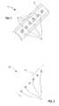
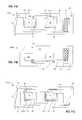
- FIG. 1shows an LED-based lighting product 10 .
- Lighting product 10includes a plurality of LED chips 30 that emit light through apertures 25 of a housing 20 .
- Housing 20may be a metal rail as shown, but may alternatively be of any desired form or material, and may include translucent or transparent materials for LED chips 30 to emit light through, in which case housing 20 need not include apertures 25 .
- FIG. 2shows a printed circuit board (“PCB”) assembly 200 with LED chips 30 assembled thereon.
- PCB assembly 200includes a PCB 40 to which LED chips 30 mount.
- PCB assembly 200is an example of a PCB assembly that may be utilized within LED-based lighting product 10 .
- FIG. 3illustrates an early stage of fabrication of a PCB 40 ( 1 ).
- PCB 40 ( 1 )includes a substrate 45 and conductors 50 .
- Substrate 45may be of known PCB substrate materials; for example, woven glass impregnated with epoxy (sometimes sold under the trade name “FR4”), cotton paper or matte glass impregnated with epoxy, woven glass impregnated with polyester.
- Conductors 50may be metal, and for example may be thick copper traces that support thermal transfer in addition to electrical connectivity.
- Conductors 50are formed on substrate 45 using known methods of PCB fabrication. Other features may also be formed on substrate 45 , for example fiducial marks may be formed for later use in aligning LED chips 30 , or cover plate subassemblies (see for example FIG. 6A , FIG. 6B , FIG. 9B , FIG. 11B , FIG. 12C and FIG. 14C ) with PCB 40 ( 1 ).
- FIG. 4illustrates components mounted to PCB 40 ( 1 ), including circuit components 60 , LED chips 30 and a standoff 80 that provides electrical and/or mechanical support for a cover plate or cover plate subassembly, as will be further illustrated below.
- Circuit components 60 , LED chips 30 and standoff 80may be soldered, or mounted with conductive epoxy, to conductors 50 (not all conductors 50 are labeled in FIG. 4 , for clarity of illustration).
- Circuit components 60may, for example, regulate power supplied to LED chips 30 .
- the epoxymay be hardened by a thermal bake or by using ultraviolet (“UV”) light.
- FIG. 4 and other drawings hereinschematically show LED chips 30 as having an N region at a “bottom” side of each chip and a P region at a “top” side of each chip, and the assembly sequence shown in FIG. 3 through FIG. 8B utilize one “backside” electrical contact and one “frontside” electrical contact.
- the P and N regionsmay be reversed from the order illustrated, and an LED chip 30 may have both P and N contacts on a top surface and that both such contacts may couple with conductors of a cover plate subassembly using the methods discussed below (in connection with FIG. 12A through FIG. 12C , for example).
- top side or frontside of an LED chipshall mean the side from which light emits from the chip
- bottom side or backsideshall mean a side opposite the frontside. That is, the backside is a side from which light does not emit or from which any light that leaks through is not used.
- FIG. 5Ais a side view of conductors 110 on a bottom surface 103 of a cover plate 100 (the terms “bottom surface” and “top surface” are understood as being in reference to a final configuration of cover plate 100 atop PCB 40 , as shown in FIGS. 8A and 8B ).
- Cover plate 100may be formed of quartz, glass, sapphire, plastic, Mylar, polycarbonate, acrylic, polyester, polyethylene and composites thereof, or other material that is transparent to light generated by LED chips 30 .
- a specific material forming cover plate 100may be chosen to have a coefficient of thermal expansion approximating that of substrate 45 , to minimize the possibility of cracking or adhesive failure with environmental stresses such as temperature cycling or vibration.
- Conductors 110may be formed of metal or may be formed of conductive but translucent or transparent materials (e.g., indium tin oxide). Conductors 110 may be formed by conventional methods such as masking and etching such that conductors 110 form a two-dimensional pattern on bottom surface 103 (see FIG. 5C ). Besides conducting electrical voltages and/or currents, conductors 110 may be utilized for identification (e.g., part numbers, barcodes) or for visual recognition and positioning (e.g., fiducial marks for alignment of cover plate 100 to LED chips or a PCB). Cover plate 100 also has a top surface 105 upon which coatings may be applied, such as for example antireflective coatings to reduce light reflections at an air interface.
- coatingse.g., part numbers, barcodes
- FIG. 5Bis a side view of cover plate 100 , similar to FIG. 5A , but with conductors 110 formed on a phosphor layer 122 that covers bottom surface 103 of cover plate 100 .
- Phosphor layer 122may fluoresce when illuminated by LED chips 30 , thus converting some of the light energy emitted by LED chips 30 into longer wavelengths to produce a better approximation of white light than the light emitted by LED chips 30 themselves.
- Phosphor layer 122is shown in FIG. 5B on bottom surface 103 , but it is understood that alternatively, phosphor layer 122 may be formed on top surface 105 of cover plate 100 .
- FIG. 5Cshows a bottom view of cover plate 100 with conductors 110 formed as two-dimensional shapes on bottom surface 103 thereof.
- Broken line 5 A- 5 Ashows a line of sight along which the views of FIGS. 5A and 5B are taken.
- FIG. 6Ais a side view of a cover plate subassembly 102 ( 1 ) that includes cover plate 100 and conductors 110 with two sections of a conformal phosphor gel 120 applied thereto.
- a conformal phosphor gel 120One or more phosphors, admixed with a gel to form phosphor gel 120 , fluoresce under light emitted by LED chips 30 , like phosphor layer 122 , FIG. 5B , discussed above.
- Phosphor gel 120may also be pliable so that, after assembly, it conforms to surface contours of LED chips 30 . Portions of phosphor gels 120 are hidden in FIG. 6A behind conductor 110 .
- FIG. 6Bis a side view of a cover plate subassembly 102 ( 1 )′ that includes cover plate 100 and conductors 110 with phosphor layer 122 (as in FIG. 5B ) and two sections of a conformal gel 120 ′ applied thereto.
- Utilizing phosphor layer 122 with conformal gel sections 120 ′may promote manufacturing flexibility and reduced cost, since it may not be necessary to remove phosphor layer 122 from areas that do not face LED chips in a final product, but conformal gel sections 120 ′ can be patterned to match an LED layout of a particular product design.
- FIG. 7Ashows cover plate subassembly 102 ( 1 ) (as shown in FIG. 6A ) with conductive epoxy 140 applied in liquid form to locations on conductors 110 that correspond to circuit connections of LED chips 30 and standoff 80 on PCB 40 ( 1 ) (as can be seen in FIG. 8A , for example—also see FIGS. 11A through 11C , 12 A through 12 C and 14 A through 14 C).
- FIG. 7Bshows cover plate subassembly 102 ( 2 ) (as shown in FIG. 6B ) with conductive epoxy 140 applied in liquid form to conductors 110 . As in FIG.
- FIG. 8Ashows a PCB assembly 200 ( 1 ) formed by mounting cover plate subassembly 102 ( 1 ), as shown in FIG. 7A , onto PCB 40 ( 1 ), as shown in FIG. 4 .
- Cover plate 100is inverted relative to the position shown in FIG. 7A , aligned to PCB 40 ( 1 ) such that conductive epoxy 140 contacts circuit connections of LED chips 30 and standoff 80 on PCB 40 ( 1 ), and is held in this orientation until conductive epoxy 140 is hardened by using UV light and/or a thermal bake.
- FIG. 8Bshows a PCB assembly 200 ( 2 ) formed by mounting cover plate subassembly 102 ( 2 ), as shown in FIG. 7B , onto PCB 40 ( 1 ), as shown in FIG.
- cover plate subassemblies 102 hereinmay be utilized for circuitry (e.g., like a PCB) to any extent consistent with the use of the cover plate itself.
- circuit componentsmay be attached to conductors 110 in addition to, or instead of, such components attaching to PCB 40 .
- FIG. 9Ashows a portion of a PCB assembly 200 ( 3 ) with reflectors 150 ( 1 ).
- Reflectors 150 ( 1 )may be formed of metal (e.g., a stamped foil such as aluminum foil), a metal coated plastic (e.g., metalized Mylar) or micromachined silicon, and may mount with conductors 50 , as shown, or may mount with cover plate 100 , as shown in FIG. 9B .
- Reflectors 150 ( 1 )serve to increase efficiency of PCB assembly 200 ( 3 ) by reflecting stray light and light emitted from sides of LED chips 30 up through cover plate 100 .
- PCB assembly 200 ( 3 )also includes a fill material 160 that fills space between a PCB 40 ( 2 ) and cover plate 100 , except space occupied by components such as LED chips 30 , standoff 80 , phosphor gel 120 and conductive epoxy 140 .
- Fill material 160may be a gel, a fluid, epoxy, a UV curable material such as silicone, or a liquid crystal material. Fill material 160 advantageously protects and/or passivates exposed surfaces of LED chips 30 and keeps contaminants out of the space between PCB 40 and cover plate 100 .
- conductors 50 and 110may be utilized to activate the liquid crystal material to modulate reflectivity of PCB assembly 200 ( 3 ).
- fill material 160may have a refractive index matched to a refractive index of cover plate 100 , thereby eliminating a Fresnel reflection that would otherwise occur at an interface between cover plate 100 and air at bottom surface 103 (e.g., see FIG. 8A ).
- FIG. 9Bshows a cover plate subassembly 102 ( 3 ) including reflectors 150 ( 2 ).
- reflectors 150 ( 2 )may be formed of metal, a metal coated plastic or micromachined silicon.
- Reflectors 150 ( 2 )attach to conductors 110 of cover plate 100 such that when assembled to a PCB with LED chips mounted thereon, reflectors 150 ( 2 ) are located between the LED chips and increase efficiency by reflecting light through cover plate 100 .
- FIG. 9Cshows a portion of a PCB assembly 200 ( 4 ) formed by mounting cover plate subassembly 102 ( 3 ) (shown in FIG. 9B ) to a PCB 40 ( 3 ) with LED chips 30 , and filling the assembly with fill material 160 .
- LED chips 30may include features and materials that cooperate with the materials and construction method detailed above.
- LED chips 30may include a phosphor coating and/or index matching gel before mounting to a PCB 40 ; such coatings may be applied in wafer form for reduced cost.
- LED chips 30may also be designed to include features such as fiducial marks that facilitate alignment of other structures thereto by humans or by machine vision (see for example FIG. 11A ). Also, although FIGS.
- LED chips 30show LED chips 30 as having an N type bottom layer accessed through a backside contact and a P type top layer accessed through a frontside contact, it is appreciated that LED chips may include topside contacts for both P and N layers, as illustrated in FIGS. 12A through 12C and FIGS. 14A through 14C .
- a layout of a PCB assembly 200may require alignment tolerances among the components thereof, leading to the layout being larger when the alignment tolerances are large.
- the larger layoutmay contribute to issues with performance (e.g., transferring heat away from the LED chips, inability to get as many LED chips as desired into a package of a given size) and/or reliability (e.g., larger cover plates and/or PCBs may be more susceptible to cracking or adhesive failure under stress).
- features that facilitate self-aligning assembly and/or machine vision for alignment purposesare now described.
- FIGS. 10A through 10Cillustrate how solder reflow may be utilized to align LED chips to a PCB.
- FIG. 10Ashows a portion of a PCB 40 ( 4 ) that includes a substrate 45 , and conductors 50 ( 1 ) sized for coupling of LED chips 30 through self-aligning solder reflow. Solder may be supplied in the form of a slug that approximately matches the outline of conductors 50 ( 1 ) where attachment of LED chips 30 is desired.
- FIG. 10Bshows LED chips 30 and solder 42 placed onto conductors 50 ( 1 ) with imperfect alignment; note that edges of LED chips 30 and solder 42 do not align vertically with edges of conductors 50 ( 1 ).
- Solder 42is then heated to a melting point of solder 42 , which melts to form a liquid 42 ′ having surface tension, as shown in FIG. 10C .
- the surface tensionis minimized by reducing area about edges of LED chips 30 and conductors 50 ( 1 ), pulling LED chips 30 into alignment with conductors 50 ( 1 ).
- liquid solder 42 ′cools and hardens into solid form, LED chips 30 remain aligned and couple with conductors 50 ( 1 ).
- solderherein is not limited to lead-tin solder but encompasses all equivalent types of low melting point metals that may include, for example, lead, tin, copper, silver, bismuth, indium, zinc and antimony.
- FIGS. 10A through 10Care particularly effective for smaller LED chips (e.g., LED chips with length and/or width less than 250 microns), as an aligning force generated in a given direction at the edges of liquid solder 42 ′ is proportional to a peripheral length of each LED chip 30 transverse to that direction, while a mass of each LED chip 30 is proportional to an area of the chip. Therefore, for a square LED chip 30 having sides of length L (as shown in FIG. 10A ) a ratio of the aligning force to the mass of a single LED chip 30 varies as 2L/L 2 . This ratio is larger for a smaller L, so a smaller LED chip is subject to a higher aligning force in proportion to its mass.
- LED chipse.g., LED chips with length and/or width less than 250 microns
- solder 42may be plated, or formed by deposition and etching, onto traces 50 ( 1 ) where attachment of LED chips 30 is desired, and/or (2) conductors 50 may extend beyond a desired bonding area for LED chips 30 , with a soldermask layer forming an opening at the desired bonding area.
- FIG. 11Ais a plan view of a portion of a PCB 40 ( 5 ) with two LED chips 30 ( 1 ) and standoff 80 mounted thereon, for subsequent coupling with cover plate subassembly 102 ( 4 ) (see FIG. 11B ) to form a PCB assembly.
- PCB 40 ( 5 )includes substrate 45 , conductors 50 and a fiducial mark 46 , as shown.
- LED chips 30 ( 1 ) and standoff 80couple with conductors 50 using solder and/or conductive epoxy.
- conductors 50are shown as slightly overlapping LED chips 30 ( 1 ) and standoff 80 , this is for illustrative clarity and it is appreciated that conductors 50 may be laid out coincidentally with LED chips 30 ( 1 ) and/or standoff 80 for purposes of self-aligning solder reflow, as discussed above in connection with FIGS. 10A through 10C .
- Each LED chip 30 ( 1 )is shown as having a light emitting area 32 , a frontside contact 34 and fiducial marks 36 in dashed outline; it is appreciated that shape, size and position of light emitting area 32 , a frontside contact 34 and fiducial marks 36 are matters of LED chip layout and may vary from the shapes shown.
- FIG. 11Bis a plan view of a cover plate subassembly 102 ( 4 ) ready for coupling with PCB 40 ( 5 ) to form a PCB assembly.
- FIG. 11Bshows bottom surface 103 of cover plate subassembly 102 ( 4 ) such that subassembly 102 ( 4 ) would be turned over top-to-bottom to couple with PCB 40 ( 5 ).
- Cover plate subassembly 102 ( 4 )includes cover plate 100 having a conductor 110 , phosphor gels 120 and a fiducial mark 146 .
- Conductive epoxy 140is shown as being placed on conductor 110 such that epoxy 140 will face frontside contacts 34 and standoff 80 when subassembly 102 ( 4 ) couples with PCB 40 ( 5 ).
- FIG. 11Cshows cover plate subassembly 102 ( 4 ), FIG. 11B , coupled with PCB 40 ( 5 ), FIG. 11A , to form PCB assembly 200 ( 5 ). Since cover plate 100 is transparent, most elements shown in FIG. 11A and FIG. 11B remain visible, but conductor 110 is opaque, hiding conductive epoxy 140 , frontside contacts 34 and one instance of fiducial mark 36 in FIG. 11C . Alignment of cover plate subassembly 102 ( 4 ) to PCB 40 ( 5 ) includes aligning fiducial mark 146 ( FIG. 11B ) to fiducial mark 46 ( FIG. 11A ) so that fiducial mark 46 is also hidden beneath fiducial mark 146 in FIG. 11C .
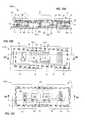
- FIG. 12Ashows a cross-sectional view of a PCB assembly 200 ( 6 ).
- PCB assembly 200 ( 6 )has two LED chips 30 ( 2 ) that each couple to a PCB 40 ( 6 ) ( FIG. 12B ) and, using two instances of conductive epoxy per LED chip 30 ( 2 ), to a cover plate subassembly 102 ( 5 ) ( FIG. 12C ).
- PCB assembly 200 ( 6 )also includes an insulating dam 170 for containing fill material 160 . Dam 170 is shown in FIG.
- FIG. 12Ashows PCB 40 ( 6 ) with LED chips 30 ( 2 ), standoffs 80 and insulating dam 170 attached thereto.
- FIG. 12Bshows PCB 40 ( 6 ) with LED chips 30 ( 2 ), standoffs 80 and insulating dam 170 attached thereto.
- FIG. 12Cshows cover plate subassembly 102 ( 5 ) with multiple instances of conductors 110 , phosphor gel 120 and conductive epoxy 140 ready for alignment to, and coupling with, PCB 40 ( 6 ) ( FIG. 12B ).
- FIG. 12Cshows cover plate subassembly 102 ( 5 ) from the perspective of facing bottom surface 103 of cover plate 100 ; optics 155 are therefore shown in dashed lines where visible through transparent cover plate 100 and phosphor gel 120 in top surface 105 (see FIG. 12A ).
- Sight lines 12 A- 12 A in each of FIG. 12B and FIG. 12Cindicate the plane at which the cross-sectional view of FIG. 12A is taken.
- FIG. 13is a flowchart showing steps of one exemplary method 300 of assembling a PCB assembly with LED chips.
- Method 300may, for example, be utilized to assemble PCB assembly 200 .
- Steps 302 through 308assemble a PCB portion of the PCB assembly, while steps 320 through 326 assemble a cover plate subassembly independently of the PCB portion.
- Steps 330 through 340join the cover plate portion to the PCB portion to form the completed PCB assembly.
- Step 302patterns conductors on a PCB (e.g., patterns conductors 50 on PCB 40 ) using known methods of PCB fabrication.
- An optional step 304shown in a dashed box, attaches circuitry (e.g., circuit components 60 ) to the PCB, either by soldering or by attaching the circuitry to the PCB using conductive epoxy. Step 304 is not applicable for products where circuit components are not needed or are not implemented on the same PCB as the LED chips (e.g., when PCB 40 includes only LED chips, and circuit functionality is implemented elsewhere).
- Step 306attaches LED chips (e.g., LED chips 30 ) to the PCB.
- An optional step 308attaches one or more standoffs (e.g., standoff 80 ), reflectors (e.g., reflector 150 ) and/or dams (e.g., dam 170 ) to the PCB.
- Steps 306 and 308may utilize solder and/or conductive epoxy; when epoxy is used, the corresponding step may include a thermal bake or UV cure to harden the epoxy.
- An optional step 320forms a phosphor layer (e.g., layer 122 ) or phosphor sections (e.g., phosphor layers 130 ) on a cover plate (e.g., on cover plate 100 ).
- Step 322patterns conductors on the cover plate (e.g., patterns conductors 110 ).
- An optional step 324attaches circuitry to the cover plate.
- An optional step 326forms a conformal index matching gel (e.g., gel 120 , 120 ′) on the cover plate.
- Step 326may be omitted (a) for cost savings, (b) when the LED chips being assembled include index matching gel and/or phosphor coating applied in wafer form, and/or (c) when fill material is to be utilized for purposes similar to those of the index matching gel.
- Step 330applies conductive epoxy to conductors, LED chips, reflectors, dams and/or standoffs on one or both of (a) the PCB prepared as in steps 302 through 308 , and (b) the cover plate subassembly prepared as in steps 320 through 326 .
- Step 332flips over the cover plate subassembly such that the conductive epoxy applied in step 330 faces the corresponding locations on the other of the cover plate portion and the PCB.
- Step 334aligns the cover plate subassembly with the PCB.
- Step 336moves the cover plate subassembly and the PCB portion together such that the epoxy couples the appropriate locations on the PCB and its components, with the appropriate locations on the cover plate subassembly.
- steps 334 and 336may be iterated, combined, or performed in a different order than that shown in FIG. 9 .
- a crude alignmentmay be performed first, followed by a crude approach of the cover plate subassembly to the PCB (at which point the conductive epoxy may or may not be in contact with both the cover plate subassembly and the PCB), followed by a fine alignment, followed by bringing the cover plate portion and the PCB portion together to a final distance from one another.
- Step 338utilizes UV light or a thermal bake to cure the conductive epoxy applied in step 330 , to complete the assembly of the PCB assembly.
- An optional step 340applies fill material to spaces between the PCB and the cover plate, as described in connection with FIG. 9A .
- FIG. 14Ashows a cross-sectional view of a PCB assembly 200 ( 7 ) that includes two LED chips 30 ( 2 ) that each couple to a PCB 40 ( 7 ) (see FIG. 14B ) and to a cover plate subassembly 102 ( 6 ) (see FIG. 14C ).
- PCB assembly 200 ( 7 )is manufactured by attaching LED chips 30 ( 2 ) to cover plate subassembly 102 ( 6 ) before cover plate assembly 102 ( 6 ) attaches to PCB assembly 200 ( 7 ), as described below.
- PCB assembly 200 ( 7 )also includes reflectors 150 ( 3 ) and 150 ( 4 ) that each have a height that is sufficient for the reflectors to function as standoffs, that is, to set a distance between PCB 40 ( 7 ) and a cover plate 100 (see FIG. 14C ).
- FIG. 14Bshows PCB 40 ( 7 ) with conductors 50 and conductive epoxy 140 applied in locations facing LED chips 30 ( 2 ) and reflectors 150 ( 3 ) and 150 ( 4 ) as shown in FIG. 14C .
- FIG. 14Cshows cover plate subassembly 102 ( 6 ) with multiple instances of conductors 110 fabricated thereon, and with LED chips 30 ( 2 ) and reflectors 150 ( 3 ) and 150 ( 4 ) attached thereto.
- Dashed lines within LED chips 30 ( 2 )show positions of light emitting areas and frontside contacts that are on the underside of LED chips 30 ( 2 ), that is, facing cover plate 100 .
- Sight lines 14 A- 14 A in each of FIG. 14B and FIG. 14Cindicate the plane at which the cross-sectional view of FIG. 14A is taken.
- FIG. 15is a flowchart showing steps of one exemplary method 500 of assembling a PCB assembly with LED chips.
- Method 500may, for example, be utilized to assemble PCB assembly 200 .
- Steps 502 through 506assemble a PCB portion of the PCB assembly, while steps 520 through 528 assemble a cover plate subassembly independently of the PCB portion.
- Steps 530 through 540join the cover plate portion to the PCB portion to form the completed PCB assembly.
- Step 502patterns conductors on a PCB (e.g., patterns conductors 50 on PCB 40 ) using known methods of PCB fabrication.
- An optional step 504shown in a dashed box, attaches circuitry (e.g., circuit components 60 ) to the PCB, either by soldering or by attaching the circuitry to the PCB using conductive epoxy. Step 504 is not applicable for products where circuit components are not needed or are not implemented on the same PCB as the LED chips (e.g., when PCB 40 includes only LED chips, and circuit functionality is implemented elsewhere).
- Optional step 506attaches one or more standoffs (e.g., standoff 80 ), reflectors (e.g., reflector 150 ) and/or dams (e.g., dam 170 ) to the PCB.
- Step 506may utilize solder and/or conductive epoxy; when epoxy is used, the corresponding step may include a thermal bake or UV cure to harden the epoxy.
- An optional step 520forms a phosphor layer (e.g., layer 122 ) or phosphor sections (e.g., phosphor layers 130 ) on a cover plate (e.g., on cover plate 100 ).
- Step 522patterns conductors on the cover plate (e.g., patterns conductors 110 ).
- An optional step 524forms a conformal index matching gel (e.g., gel 120 , 120 ′) on the cover plate. Step 524 may be omitted (a) for cost savings, (b) when the LED chips being assembled include index matching gel and/or phosphor coating applied in wafer form, and/or (c) when fill material is to be utilized for purposes similar to those of the index matching gel.
- An optional step 526attaches circuitry to the cover plate.
- Step 528attaches the LED chips to the cover plate.
- Step 530applies conductive epoxy to one or the other of conductors, LED chips, reflectors, dams and/or standoffs on the PCB prepared as in steps 502 through 508 , and/or the cover plate subassembly prepared as in steps 520 through 524 .
- Step 532flips over the cover plate subassembly such that the conductive epoxy applied in step 530 faces the corresponding locations on the other of the cover plate portion and the PCB.
- Step 534aligns the cover plate subassembly with the PCB.
- Step 536moves the cover plate subassembly and the PCB portion together such that the epoxy couples the appropriate locations on the PCB and its components, with the appropriate locations on the cover plate subassembly.
- steps 534 and 536may be iterated, combined or performed in a different order than that shown in FIG. 9 .
- a crude alignmentmay be performed first, followed by a crude approach of the cover plate subassembly to the PCB (at which point the conductive epoxy may or may not be in contact with both the cover plate subassembly and the PCB), followed by a fine alignment, followed by bringing the cover plate portion and the PCB portion together to a final distance from one another.
- Step 538utilizes UV light or a thermal bake to cure the conductive epoxy applied in step 530 , to complete the assembly of the PCB assembly.
- An optional step 540applies fill material to spaces between the PCB and the cover plate, as described in connection with FIG. 9A .
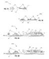
- FIG. 16Aschematically shows a prior art LED lighting product 600 .
- Lighting product 600includes a mechanical fixture 602 in which are mounted LED light modules 604 .
- Each light module 604includes an array of three large LED chips 30 ( 3 ).
- FIG. 16Bshows an LED chip-based lighting product 650 .
- Lighting product 650includes a panel 654 within a frame 656 .
- Lighting product 650may be, for example, a troffer.
- Panel 654may be made of (a) an electrically insulating material, or (b) an electrically conductive material coated with an insulating material; for example, panel 654 may be a painted metal panel.
- Many small LED chips 30 ( 4 )mount on a first surface 653 of panel 654 .
- LED chips 30 ( 4 )are, for example, stochastically arranged on first surface 653 such that no lines, grids or other regular patterns are evident.
- LED chips 30 ( 4 )may range in size from 0.25 mm 2 to 4 mm 2 .
- a second surface 652 of panel 654counterfaces first surface 653 ; that is, surface 652 is on an opposite side of panel 654 from surface 653 . At least part of second surface 652 is an external surface of lighting product 650 .
- one or more of LED chips 30 ( 4 )are attached by wirebonds to conductors formed on first surface 653 (e.g., see FIG. 18 ).
- one or more of LED chips 30 ( 4 )may couple with a cover plate assembly as substantially described above and illustrated in FIGS. 11A-11C .
- the stochastic arrangement of LED chips, use of small chips, and their use on a panel that forms an external surface of lighting product 650is advantageous from the perspective of a user for several reasons, including: (1) Human users often find regular patterns of visible objects such as light sources distracting, and such patterns can cast light in stripes or other distracting light patterns, whereas stochastic arrangements are less distracting and may cast light more evenly. (2) The smaller LED chips produce less light per chip, such that the individual point sources do not produce discomfort if viewed directly. (3) Smaller LED chips may be more efficient than larger LED chips at emitting all of the light produced, so that net energy efficiency is higher.
- each LED chip 30 ( 4 )does not pass first to a PCB, then to other structures of lighting product 650 ; instead, the backside of each chip 30 ( 4 ) forms a direct thermal interface, as defined below, through second surface 652 of panel 654 and then to ambient air.
- Lighting product 650may include transmissive or translucent screens or diffusers as discussed below; such screens or diffusers are not shown in FIG. 16B for clarity of illustration.
- FIG. 17Ais a cross-sectional view of LED chip-based lighting product 650 .
- LED chips 30 ( 4 )are shown mounted with conductors 658 on first surface 653 of panel 654 , so that one of the electrical contacts of each LED chip is through one of the conductors 658 .
- LED chips 30 ( 4 )mount directly to first surface 653 of panel 654 and all electrical connections are made through the top side of each LED chip.
- a frame 656attaches to panel 654 and holds an optional diffuser 660 .
- Second surface 652 of panel 654 , counterfacing first surface 653is an external surface of lighting product 650 and is in thermal communication with ambient air 670 .
- ambient airherein denotes air entirely outside a lighting product, and excludes air within enclosed cavities of the lighting product.
- all of second side 652forms an external surface of lighting product 650 ; however in other embodiments an external surface may be formed by only a portion of a second side of a panel.
- a region within LED chip-based lighting product 650is denoted as A and is described in further detail below.
- FIG. 17Bis a detail view of region A shown in FIG. 17A . Spacings between adjacent LED chips 30 ( 4 ) are denoted as S. While the value of S varies among the various adjacent pairs of LED chips 30 ( 4 ) in lighting product 650 , an average value S avg of all such adjacent pairs of LED chips may be determined. Also in FIG. 17B , a standoff distance from surfaces of LED chips 30 ( 4 ) to optional diffuser 660 is denoted as D.
- DWhen D is greater than or equal to about two times S avg , light from adjacent LED chips 30 ( 4 ) blends together on diffuser 660 such that an overall light distribution from lighting product 650 appears to a user as a somewhat homogeneous lighted area, instead of a collection of individual points or spots of light.
- the appearance of a lighted area instead of points of lightmay be preferable and less distracting to a user of lighting product 650 .
- a region within region Ais denoted as B and is described in further detail below.
- FIG. 17Cis a detail view of region B shown in FIG. 17B and shows LED chip 30 ( 4 ) mounted with conductor 658 formed on first surface 653 of panel 654 .
- a backside surface of LED chip 30 ( 4 ) that faces conductor 658is shown as mounting surface 672 .
- An arrow Tillustrates a direct thermal interface from LED chip 30 ( 4 ) that extends perpendicularly through mounting surface 672 , conductor 658 and panel 654 to ambient air 670 .
- direct thermal interfacewhen used in connection with an LED chip, denotes an arrangement of at most one conductor, one panel and intervening mounting materials (e.g., solder, epoxy or adhesive) that extends perpendicularly from a backside of the LED chip to ambient air.
- a direct thermal interfacethus excludes arrangements that require heat transfer in one or more lateral directions (any direction that is not perpendicular to an LED chip's mounting surface, e.g., surface 672 ) to reach ambient air, and arrangements that transfer heat from an LED to enclosed cavities.
- direct thermal interfacedenotes a similar arrangement of at most one conductor, one panel and intervening mounting materials (e.g., solder, epoxy or adhesive) that extends perpendicularly away from a light emitting side of the packaged LED to ambient air.
- intervening mounting materialse.g., solder, epoxy or adhesive
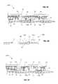
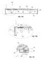
- FIG. 18shows a portion of an embodiment of an LED chip-based lighting product 700 .
- Lighting product 700includes a connection 704 to an external power source.
- Connection 704may be, for example, a power cord or wiring enclosed within a conduit.
- the external power source(not shown) connects, through connection 704 , to optional power conversion electronics 701 through an aperture 703 in a light fixture 702 .
- Power conversion electronics 701may include power conditioning and control components, for example (a) to convert AC power to DC power, and (b) to regulate voltage and/or current of the DC power as needed for LEDs (e.g., to convert high input voltage to a maximum voltage usable with LEDs, and/or to vary light output of the LEDs for dimming); steps (a) and (b) may be done in any order or repeatedly.
- Conductors 706are formed on an upper panel 710 of light fixture 702 by conventional means such as silk screening, inkjet printing, photolithography, electroplating and/or other methods known in the art. LED chips 30 mount to one or more conductors 706 , typically through the use of automated pick and place equipment.
- FIG. 18shows LED chips 30 connected to power conductor 706 ( 2 ) via wirebonds 712 , but other means of establishing connections from LED chips 30 to conductor(s) may be used. Also, it is appreciated that if LED chips 30 are fabricated with two backside electrical connections (e.g., on the opposite side of the chips from their emitting surfaces), that connections may be made to conductors 706 with the electrical connections facing downwardly (e.g., facing panel 710 ) and the emitting surface facing upwardly (e.g., emitting outwards from panel 710 ). (Not all LEDs 30 or their associated wirebonds 712 are labeled in FIG. 17 , for clarity of illustration.) Conductors 706 are shown in FIG.
- ground conductor 7061
- power conductor 7062
- conductors 706may be routed in any convenient fashion utilizing automatic routing tools as are known in the art of PCB design.
- Power conversion electronics 701supply electrical power to conductors 706 via electrical traces 705 that may be, for example, leads extending from power conversion electronics 701 that are soldered to conductors 706 .
- LED chips 30are mounted onto conductors 706 using conductive epoxy, solder, or other known materials and methods for attaching semiconductor chips to substrates.
- LED chips 30may, optionally, be coated with one or more materials that may include protective substance(s) for protection from contaminants and/or phosphors for downconverting wavelength of a portion of the light emitted by each LED to a longer wavelength (e.g., to create “white” light from LED chips emitting mostly blue light).
- one or more cover platesmay be applied to individual LED chips, groups of LED chips or an entire fixture.
- extra heat sinkssuch as fins (not shown) may be added to light fixture 702 to further promote heat dissipation.
- FIG. 19shows one exemplary flowchart of a method 800 for assembling LED chip based lighting products.
- Method 800describes assembly of a lighting product exemplified as based on a mechanical fixture for a troffer type lighting product; however it is appreciated by those skilled in the art that the techniques described therein may be adapted to assembly of other lighting products. It is also appreciated that certain steps of method 800 may be omitted or performed in an order different than that shown in FIG. 18 .
- Step 810patterns conductors on a panel that will eventually form a top inside surface of the lighting product.
- method 800takes advantage of the fact that the step of patterning the conductors (e.g., screen printing, or photolithography and etching of conductive layers) may be more easily performed on a flat panel, than on a panel that is not flat.
- Step 810may implement a stochastic layout for a large number of LEDS on the panel, as discussed previously.
- Method 800alternatively includes step 820 or step 822 , which are shown as following step 810 , but it is appreciated that step 820 or 822 may be performed later in method 800 , such as after any of steps 830 , 840 and 850 , discussed below.
- Step 820bends the panel to form the mechanical fixture
- step 822mounts the panel to a frame to form the mechanical fixture.
- step 822involves mounting (e.g., screwing or bolting) a frame to edges of the panel.
- step 822may place the panel with LED chips atop another panel and the two panels may be bonded together.
- one of the panelsis preferably ductile or compliant such that intimate thermal contact is provided between the panels when dust or other contamination blocks direct contact between the two panels at one location.
- a thermally conductive paste or adhesivemay be utilized to join the two panels.
- Step 830mounts LED chips to the conductors.
- step 830may include picking and placing the LED chips from stretched tape or from die carriers, and may include affixing the LED chips to the conductors utilizing conductive epoxy, solder, or other known methods for attaching a chip to a conductor.
- An optional step 840forms top side electrical connections of the LED chips to the lighting product. Step 840 is not needed when step 830 includes establishing all needed electrical connections of the LED chips through their bottom sides (e.g., when the LED chips have both P and N contacts on their bottom sides).
- Step 840may include, for example, forming wirebond connections from bonding pads on top sides of the LED chips to the conductors formed on the panels in step 810 .
- Step 840may also be performed in conjunction with step 860 discussed below, when protective material in the form of a cover panel is affixed over the LEDs.
- Step 850mounts external electrical connections, and non-LED electrical components, to the mechanical fixture.
- step 850establishes some means for transferring electrical power into the fixture; the electrical power may be controlled external to the fixture, or means for transferring raw power (e.g., 120VAC power) may be established, along with power conditioning and control elements to convert the raw power into an appropriate power source for the LEDs.
- raw powere.g. 120VAC power
- an external power connection in the form of wires in a conduitmay be brought through an aperture in one side of the fixture, the wires may connect to a PCB having power conditioning components thereon, and conditioned power for the LEDs may be transferred to the conductors by connections soldered between the PCB and the conductors.
- Step 860applies one or more materials, such as protective materials and/or phosphors, to the LED chips and/or to other components (e.g., the components mounted in step 850 ).
- transparent epoxyis applied over each LED chip so that when the epoxy cures, the LED chip is protected but can emit light through the epoxy.
- the epoxymay include one or more phosphors for downconverting a portion of the light from the LEDs to longer wavelengths.
- step 860is mounting one or more cover plates or lenses over one or more LED chips at a time, as described in conjunction with FIGS. 8A through 14C . A single cover plate may be applied over the entire panel.
- electrical connectionsmay be formed simultaneously and fill materials, optionally including a phosphor, may be applied, as also described in conjunction with FIGS. 8A through 14C . It is appreciated that application of a phosphor alone may take place for example between steps 830 and 840 ; that is, the phosphor may be applied to mounted LED chips before wirebonding occurs, so as to minimize risk of damage to wirebonds by applying the phosphor later.
- An optional step 870adds diffusers and/or heat sinks to the lighting product.
- Diffusersserve to further spread out light from the individual LED chips to reduce glare, and may be transparent, translucent or grate type elements.
- Grate type elementsserve to reduce cut-off angle of a light fixture, which is an angle from a user to a light fixture where the light emitting elements themselves are no longer visible to the user.
- Human users of lighting productsoften prefer high cut-off angles, that is, the users find it preferable not to be subjected to glare of light sources more or less in their line of sight, but rather to have such sources at a high angle where human eyebrows form a natural glare shield.
- Grate type elementsmay be particularly advantageous in LED chip-based lighting products, by serving the dual functions of increasing cut-off angle and as additional heat sinking elements.
- Another type of diffuser that may be particularly advantageousis a diffuser that forms upwardly pointed shapes (e.g., pointed towards the LED chips), as each such shape will tend to split light incident upon it into a set of rays at differing angles. In so doing, from a user's standpoint, the shapes divide each point source into a distributed set of point sources, thus effectively splitting the light sources into multiple, fainter light sources that will be less distracting than the original, brighter sources.
- Transparent and translucent diffuserscan also include phosphors or pigments for adjusting the spectral output of the lighting product.
- Heat sinksmay also be applied in step 870 —typically to the top side of the panel (opposite the side where the LEDs are mounted)—to improve heat transfer away from the lighting product.
- the productmay also be ventilated to encourage convective flow for heat removal. This runs counter to the prevailing practice in design of fluorescent fixtures, in which heat is often intentionally concentrated by providing a closed cabinet, since fluorescent ballasts and tubes are often more efficient at high temperatures.
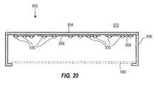
- FIG. 20shows a cross section of an LED-based lighting product 950 that mounts packaged LEDs 930 directly onto conductors 958 patterned on a panel 954 .
- a first surface of panel 954counterfaces a second surface of panel 954 , and at least a part of the second side forms an exterior surface of lighting product 950 .
- One or more of LEDs 930is mounted to form a direct thermal interface to ambient air 970 through only conductors 958 and panel 954 .
- LEDs 930may be low power LEDs and are mounted in a widely distributed stochastic arrangement (e.g., like LED chips 30 ( 4 ) on panel 654 , FIG. 16B .
- a frame 956attaches to panel 954 and holds an optional diffuser 960 at a distance from LEDs 930 at least twice an average spacing between adjacent LEDs 930 on panel 954 (the distance and spacing are not labeled in FIG. 20 but may be determined in the same way as the distance and spacing illustrated for LED chips in FIG. 17B ).
- lighting product 950streamlines thermal dissipation and lowers manufacturing cost as compared with an approach that first mounts packaged LEDs on a PCB or other module, then mounts the module in a lighting product.
- a common 4′ ⁇ 2′ troffer fixtureprovides 8 square feet of surface area that is used as a heat sink.
- the fixtureis constructed of aluminum which results in a 4 ⁇ increase of thermal conductivity compared to steel.
- Electrical connections to the LED chipsare patterned onto the light fixture by known screen printing, inkjet technology or other means. Automated pick and place equipment places the LED chips in the correct positions, and wire bond equipment is used to connect the electrical traces.
- Five hundred 50 micron LED chipsare stochastically distributed as a widely distributed stochastic arrangement over the 8 square feet of the aluminum fixture. Each 50 micron LED chip delivers a lumen output of 10 lumens. Thus the stochastic array of 500 LED chips produces a 5000 lumen output.
- Each LED chipis driven at around 3.4 V in the 30 mA to 50 mA range, resulting in a power distribution of approximately 6 to 10 W/ft 2 , and the resulting heat is efficiently dissipated through a direct thermal interface from each LED chip to ambient air.
- Light distributionis maximized through the use of high efficiency first surface diffuse reflectors with optical cavity structures to both minimize glare and optimize light distribution.
- a temperature increase (LED to ambient air) generatedis between about 20° F. to about 60° F. depending upon the exact configuration of the troffer and the stochastic array. Modification of the troffer fixture may includes additional thermal fins or heat sinks, should additional cooling be desired.
- a larger LED chiphas a longer path length l, which leads to higher resistance (Eq. 3) and thus higher ohmic power loss for a given current I (Eq. 2).
- Eq. 3higher resistance
- IEq. 2
- Directly mounting the LEDs in the fixtureeliminates many cost components, flattens the supply chain, and provides a viable path to achieving performance and cost goals. Furthermore, many additional benefits may be realized, such as improved thermal dissipation, lowered complexity and cost of the thermal dissipation system, lower demand on drive circuitry, improved drive circuitry reliability and greater overall system redundancy and reliability.
- Phosphor layers and typesmay be single or multiple (for example, to provide multiple fluorescence wavelengths for broad spectrum light) and phosphors may be admixed with epoxies, conformal gels, index matching gels, fill material or cover plate materials.
Landscapes
- Led Device Packages (AREA)
Abstract
Description
V=I·R(“Ohm's law”), (Eq. 1)
- where V=voltage, R=resistance and I=current,
- which can be restated as:
P=I2·R (Eq. 2) - where P=V·I=power loss through ohmic resistance; and
R(spreading resistance)=l·A·ρ (Eq. 3) - where l is the path length, A is cross-sectional area of an LED, and ρ is the bulk resistivity of the LED material (resistance per unit volume).
Claims (22)
Priority Applications (5)
| Application Number | Priority Date | Filing Date | Title |
|---|---|---|---|
| US12/857,472US8058659B2 (en) | 2008-08-26 | 2010-08-16 | LED chip-based lighting products and methods of building |
| US13/287,796US8338197B2 (en) | 2008-08-26 | 2011-11-02 | LED chip-based lighting products and methods of building |
| US13/718,755US8558255B2 (en) | 2008-08-26 | 2012-12-18 | LED chip-based lighting products and methods of building |
| US13/802,444US9076951B2 (en) | 2008-08-26 | 2013-03-13 | Methods of integrating LED chips with heat sinks, and LED-based lighting assemblies made thereby |
| US13/802,401US8981629B2 (en) | 2008-08-26 | 2013-03-13 | Methods of integrating LED chips with heat sinks, and LED-based lighting assemblies made thereby |
Applications Claiming Priority (3)
| Application Number | Priority Date | Filing Date | Title |
|---|---|---|---|
| US12/198,662US7791089B2 (en) | 2008-08-26 | 2008-08-26 | LED packaging methods and LED-based lighting products |
| US23430909P | 2009-08-16 | 2009-08-16 | |
| US12/857,472US8058659B2 (en) | 2008-08-26 | 2010-08-16 | LED chip-based lighting products and methods of building |
Related Parent Applications (1)
| Application Number | Title | Priority Date | Filing Date |
|---|---|---|---|
| US12/198,662Continuation-In-PartUS7791089B2 (en) | 2008-08-26 | 2008-08-26 | LED packaging methods and LED-based lighting products |
Related Child Applications (1)
| Application Number | Title | Priority Date | Filing Date |
|---|---|---|---|
| US13/287,796DivisionUS8338197B2 (en) | 2008-08-26 | 2011-11-02 | LED chip-based lighting products and methods of building |
Publications (3)
| Publication Number | Publication Date |
|---|---|
| US20100308350A1 US20100308350A1 (en) | 2010-12-09 |
| US20110121324A2 US20110121324A2 (en) | 2011-05-26 |
| US8058659B2true US8058659B2 (en) | 2011-11-15 |
Family
ID=43300112
Family Applications (3)
| Application Number | Title | Priority Date | Filing Date |
|---|---|---|---|
| US12/857,472ActiveUS8058659B2 (en) | 2008-08-26 | 2010-08-16 | LED chip-based lighting products and methods of building |
| US13/287,796Expired - Fee RelatedUS8338197B2 (en) | 2008-08-26 | 2011-11-02 | LED chip-based lighting products and methods of building |
| US13/718,755ActiveUS8558255B2 (en) | 2008-08-26 | 2012-12-18 | LED chip-based lighting products and methods of building |
Family Applications After (2)
| Application Number | Title | Priority Date | Filing Date |
|---|---|---|---|
| US13/287,796Expired - Fee RelatedUS8338197B2 (en) | 2008-08-26 | 2011-11-02 | LED chip-based lighting products and methods of building |
| US13/718,755ActiveUS8558255B2 (en) | 2008-08-26 | 2012-12-18 | LED chip-based lighting products and methods of building |
Country Status (1)
| Country | Link |
|---|---|
| US (3) | US8058659B2 (en) |
Cited By (34)
| Publication number | Priority date | Publication date | Assignee | Title |
|---|---|---|---|---|
| US20110163681A1 (en)* | 2011-02-22 | 2011-07-07 | Quarkstar, Llc | Solid State Lamp Using Modular Light Emitting Elements |
| US20120168919A1 (en)* | 2011-01-04 | 2012-07-05 | Eom Joo-Yang | Semiconductor package and method of fabricating the same |
| US8414154B2 (en) | 2010-11-01 | 2013-04-09 | Quarkstar Llc | Solid state bidirectional light sheet having vertical orientation |
| US8629475B2 (en) | 2012-01-24 | 2014-01-14 | Cooledge Lighting Inc. | Light-emitting dies incorporating wavelength-conversion materials and related methods |
| WO2014087047A1 (en) | 2012-12-03 | 2014-06-12 | Lumichip Limited | A hermetically sealed optoelectronic component |
| US20140168954A1 (en)* | 2012-12-14 | 2014-06-19 | David Gershaw | Led panel light fixture |
| US8791640B2 (en) | 2011-02-22 | 2014-07-29 | Quarkstar Llc | Solid state lamp using light emitting strips |
| US8896010B2 (en) | 2012-01-24 | 2014-11-25 | Cooledge Lighting Inc. | Wafer-level flip chip device packages and related methods |
| US8907362B2 (en) | 2012-01-24 | 2014-12-09 | Cooledge Lighting Inc. | Light-emitting dies incorporating wavelength-conversion materials and related methods |
| US9062867B2 (en) | 2012-12-12 | 2015-06-23 | Cree, Inc. | LED lamp |
| USD740972S1 (en) | 2013-09-25 | 2015-10-13 | Cree, Inc. | Lamp |
| US9169977B2 (en) | 2013-06-28 | 2015-10-27 | Cree, Inc. | LED lamp |
| US9222659B2 (en) | 2013-06-28 | 2015-12-29 | Cree, Inc. | LED lamp |
| USD749768S1 (en) | 2014-02-06 | 2016-02-16 | Cree, Inc. | Troffer-style light fixture with sensors |
| US9273835B2 (en) | 2010-12-08 | 2016-03-01 | Cree, Inc. | Linear LED lamp |
| US9316368B2 (en) | 2011-04-18 | 2016-04-19 | Cree, Inc. | LED luminaire including a thin phosphor layer applied to a remote reflector |
| US9328876B2 (en) | 2014-03-19 | 2016-05-03 | Cree, Inc. | High efficiency LED lamp |
| US9328874B2 (en) | 2014-03-25 | 2016-05-03 | Cree, Inc. | LED lamp |
| US9343444B2 (en) | 2014-02-05 | 2016-05-17 | Cooledge Lighting, Inc. | Light-emitting dies incorporating wavelength-conversion materials and related methods |
| US9388948B2 (en) | 2014-03-25 | 2016-07-12 | Cree, Inc. | LED lamp |
| US9423116B2 (en) | 2013-12-11 | 2016-08-23 | Cree, Inc. | LED lamp and modular lighting system |
| US9476566B2 (en) | 2012-01-06 | 2016-10-25 | Cree, Inc. | Light fixture with textured reflector |
| US9488329B2 (en) | 2012-01-06 | 2016-11-08 | Cree, Inc. | Light fixture with textured reflector |
| USD772465S1 (en) | 2014-02-02 | 2016-11-22 | Cree Hong Kong Limited | Troffer-style fixture |
| US9512977B2 (en) | 2012-01-26 | 2016-12-06 | Cree, Inc. | Reduced contrast LED lighting system |
| US9534765B2 (en) | 2011-07-24 | 2017-01-03 | Cree, Inc. | Light fixture with coextruded components |
| US9726330B2 (en) | 2013-12-20 | 2017-08-08 | Cree, Inc. | LED lamp |
| US9765935B2 (en) | 2014-03-25 | 2017-09-19 | Cree, Inc. | LED lamp with LED board brace |
| USD807556S1 (en) | 2014-02-02 | 2018-01-09 | Cree Hong Kong Limited | Troffer-style fixture |
| US9927100B2 (en) | 2014-03-25 | 2018-03-27 | Cree, Inc. | LED lamp with LED board brace |
| US10012354B2 (en) | 2015-06-26 | 2018-07-03 | Cree, Inc. | Adjustable retrofit LED troffer |
| US10203088B2 (en) | 2011-06-27 | 2019-02-12 | Cree, Inc. | Direct and back view LED lighting system |
| US10527225B2 (en) | 2014-03-25 | 2020-01-07 | Ideal Industries, Llc | Frame and lens upgrade kits for lighting fixtures |
| US10891881B2 (en) | 2012-07-30 | 2021-01-12 | Ultravision Technologies, Llc | Lighting assembly with LEDs and optical elements |
Families Citing this family (33)
| Publication number | Priority date | Publication date | Assignee | Title |
|---|---|---|---|---|
| US8308320B2 (en) | 2009-11-12 | 2012-11-13 | Cooper Technologies Company | Light emitting diode modules with male/female features for end-to-end coupling |
| WO2011139764A2 (en) | 2010-04-27 | 2011-11-10 | Cooper Technologies Company | Linkable linear light emitting diode system |
| WO2011139768A2 (en) | 2010-04-28 | 2011-11-10 | Cooper Technologies Company | Linear led light module |
| US8198109B2 (en) | 2010-08-27 | 2012-06-12 | Quarkstar Llc | Manufacturing methods for solid state light sheet or strip with LEDs connected in series for general illumination |
| US8957430B2 (en)* | 2011-06-15 | 2015-02-17 | Cree, Inc. | Gel underfill layers for light emitting diodes |
| US8525190B2 (en) | 2011-06-15 | 2013-09-03 | Cree, Inc. | Conformal gel layers for light emitting diodes |
| KR101824011B1 (en)* | 2011-07-29 | 2018-01-31 | 엘지이노텍 주식회사 | Light-emitting device |
| US20140209928A1 (en)* | 2011-09-22 | 2014-07-31 | The Silanna Group Pty Ltd | Light source assembly and a process for producing a light source assembly |
| CN102638933A (en)* | 2012-04-24 | 2012-08-15 | 叶彬 | Circuit board for LED (light-emitting diode) and LED streetlight for circuit board |
| US20140168961A1 (en)* | 2012-12-18 | 2014-06-19 | Jack Guy Dubord | Retrofit kit for fluorescent lamp fixtures |
| US20140209961A1 (en)* | 2013-01-30 | 2014-07-31 | Luxo-Led Co., Limited | Alternating current light emitting diode flip-chip |
| US10094523B2 (en)* | 2013-04-19 | 2018-10-09 | Cree, Inc. | LED assembly |
| US9338850B2 (en)* | 2013-04-24 | 2016-05-10 | GE Lighting Solutions, LLC | Lighting systems and methods providing active glare control |
| CN103311419A (en)* | 2013-06-24 | 2013-09-18 | 量一光电科技(惠州)有限公司 | Method of improving lighting effect of COB (chip on board) light source |
| US9093415B2 (en)* | 2013-09-25 | 2015-07-28 | Stats Chippac Ltd. | Integrated circuit packaging system with heat spreader and method of manufacture thereof |
| KR101584201B1 (en) | 2014-01-13 | 2016-01-13 | 삼성전자주식회사 | Semiconductor light emitting device |
| DE102014110614A1 (en)* | 2014-07-28 | 2016-01-28 | Osram Opto Semiconductors Gmbh | Electronic component and method for producing an electronic component |
| KR102198695B1 (en) | 2014-09-03 | 2021-01-06 | 삼성전자주식회사 | Light source module and backlight unit having the same |
| US11480305B2 (en) | 2014-09-25 | 2022-10-25 | Jiaxing Super Lighting Electric Appliance Co., Ltd. | LED tube lamp |
| CN112197181A (en) | 2014-09-28 | 2021-01-08 | 嘉兴山蒲照明电器有限公司 | LED straight lamp |
| US10560989B2 (en) | 2014-09-28 | 2020-02-11 | Jiaxing Super Lighting Electric Appliance Co., Ltd | LED tube lamp |
| GB201418772D0 (en)* | 2014-10-22 | 2014-12-03 | Infiniled Ltd | Display |
| US12264789B2 (en) | 2014-12-05 | 2025-04-01 | Jiaxing Super Lighting Electric Appliance Co., Ltd | LED tube lamp |
| US10514134B2 (en) | 2014-12-05 | 2019-12-24 | Jiaxing Super Lighting Electric Appliance Co., Ltd | LED tube lamp |
| US10352541B2 (en)* | 2015-01-30 | 2019-07-16 | Signify Holding B.V. | Integrated smart module architecture |
| US9897265B2 (en) | 2015-03-10 | 2018-02-20 | Jiaxing Super Lighting Electric Appliance Co., Ltd. | LED tube lamp having LED light strip |
| KR102466959B1 (en) | 2015-12-31 | 2022-11-11 | 엘지디스플레이 주식회사 | Organic Light Emitting Display Device |
| US20180190672A1 (en)* | 2017-01-03 | 2018-07-05 | Innolux Corporation | Display device |
| US10260683B2 (en) | 2017-05-10 | 2019-04-16 | Cree, Inc. | Solid-state lamp with LED filaments having different CCT's |
| CN207969020U (en)* | 2018-02-06 | 2018-10-12 | 广东欧曼科技股份有限公司 | Low-pressure lamp band |
| CN115951521A (en)* | 2018-04-19 | 2023-04-11 | 群创光电股份有限公司 | Light emitting module and display device |
| CN219453696U (en) | 2021-01-27 | 2023-08-01 | 嘉兴山蒲照明电器有限公司 | LED straight tube lamp and lighting system |
| US11920743B2 (en) | 2021-12-01 | 2024-03-05 | Jiaxing Super Lighting Electric Appliance Co., Ltd | LED tube lamp |
Citations (14)
| Publication number | Priority date | Publication date | Assignee | Title |
|---|---|---|---|---|
| US5283425A (en) | 1992-02-06 | 1994-02-01 | Rohm Co., Ltd. | Light emitting element array substrate with reflecting means |
| US6568833B2 (en) | 2000-06-28 | 2003-05-27 | Oxley Developments Company Limited | Light |
| US6982518B2 (en) | 2003-10-01 | 2006-01-03 | Enertron, Inc. | Methods and apparatus for an LED light |
| US7170100B2 (en) | 2005-01-21 | 2007-01-30 | Luminus Devices, Inc. | Packaging designs for LEDs |
| US7252408B2 (en) | 2004-07-19 | 2007-08-07 | Lamina Ceramics, Inc. | LED array package with internal feedback and control |
| US20070222369A1 (en)* | 2003-08-28 | 2007-09-27 | Mitsubishi Chemical Corporation | Light-emitting device and phosphor |
| US7303315B2 (en) | 2004-11-05 | 2007-12-04 | 3M Innovative Properties Company | Illumination assembly using circuitized strips |
| US7309151B2 (en) | 2005-04-11 | 2007-12-18 | Avago Technologies Ecbu Ip (Singapore) Pte. Ltd. | Light emitting panel |
| US7358929B2 (en) | 2001-09-17 | 2008-04-15 | Philips Solid-State Lighting Solutions, Inc. | Tile lighting methods and systems |
| US7476557B2 (en) | 2004-03-29 | 2009-01-13 | Articulated Technologies, Llc | Roll-to-roll fabricated light sheet and encapsulated semiconductor circuit devices |
| US7549773B2 (en) | 2005-12-29 | 2009-06-23 | Lam Chiang Lim | LED housing |
| US20090267085A1 (en) | 2005-03-11 | 2009-10-29 | Seoul Semiconductor Co., Ltd. | Led package having an array of light emitting cells coupled in series |
| US7626208B2 (en)* | 2006-03-17 | 2009-12-01 | Industrial Technology Research Institute | Bendable solid state planar light source structure |
| US20100244056A1 (en)* | 2007-05-31 | 2010-09-30 | Nthdegree Technologies Worldwide Inc. | Addressable Or Static Light Emitting, Power Generating Or Other Electronic Apparatus |
Family Cites Families (69)
| Publication number | Priority date | Publication date | Assignee | Title |
|---|---|---|---|---|
| ATE47624T1 (en) | 1984-11-15 | 1989-11-15 | Japan Traffic Manage Tech Ass | SIGNAL LIGHT UNIT WITH HEAT DISSIPATION. |
| JPH0750799B2 (en) | 1986-04-17 | 1995-05-31 | 株式会社東芝 | Light emitting device |
| DE3929955A1 (en) | 1989-09-08 | 1991-03-14 | Inotec Gmbh Ges Fuer Innovativ | LIGHT SPOTLIGHTS |
| JPH0487381A (en) | 1990-07-31 | 1992-03-19 | Eastman Kodak Japan Kk | light emitting diode array chip |
| US5119174A (en) | 1990-10-26 | 1992-06-02 | Chen Der Jong | Light emitting diode display with PCB base |
| US5082422A (en) | 1991-06-10 | 1992-01-21 | Wang Sui Mu | Illuminative fan |
| US5241360A (en) | 1992-02-06 | 1993-08-31 | Cubic Automatic Reveneu Collection Group | Distance measuring device utilizing semiconductor laser |
| US5278432A (en) | 1992-08-27 | 1994-01-11 | Quantam Devices, Inc. | Apparatus for providing radiant energy |
| US5534718A (en) | 1993-04-12 | 1996-07-09 | Hsi-Huang Lin | LED package structure of LED display |
| US6045240A (en) | 1996-06-27 | 2000-04-04 | Relume Corporation | LED lamp assembly with means to conduct heat away from the LEDS |
| US5785418A (en) | 1996-06-27 | 1998-07-28 | Hochstein; Peter A. | Thermally protected LED array |
| US5857767A (en) | 1996-09-23 | 1999-01-12 | Relume Corporation | Thermal management system for L.E.D. arrays |
| US20030133292A1 (en) | 1999-11-18 | 2003-07-17 | Mueller George G. | Methods and apparatus for generating and modulating white light illumination conditions |
| US6367949B1 (en) | 1999-08-04 | 2002-04-09 | 911 Emergency Products, Inc. | Par 36 LED utility lamp |
| US6712486B1 (en) | 1999-10-19 | 2004-03-30 | Permlight Products, Inc. | Mounting arrangement for light emitting diodes |
| US6354714B1 (en) | 2000-04-04 | 2002-03-12 | Michael Rhodes | Embedded led lighting system |
| WO2001095673A1 (en) | 2000-06-06 | 2001-12-13 | 911 Emergency Products, Inc. | Led compensation circuit |
| GB2361989A (en)* | 2000-07-17 | 2001-11-07 | Designedge Europ Ltd | Luminaire which is edge-illuminated by an array of LEDs |
| DE10063876B4 (en) | 2000-12-21 | 2009-02-26 | Continental Automotive Gmbh | From a variety of LEDs existing light source |
| AU2002251807A1 (en) | 2001-01-23 | 2002-08-19 | Donnelly Corporation | Improved vehicular lighting system for a mirror assembly |
| US6561678B2 (en) | 2001-02-05 | 2003-05-13 | James F. Loughrey | Variable focus indirect lighting fixture |
| TW567619B (en) | 2001-08-09 | 2003-12-21 | Matsushita Electric Industrial Co Ltd | LED lighting apparatus and card-type LED light source |
| US6871981B2 (en) | 2001-09-13 | 2005-03-29 | Heads Up Technologies, Inc. | LED lighting device and system |
| US6609804B2 (en) | 2001-10-15 | 2003-08-26 | Steven T. Nolan | LED interior light fixture |
| KR20040074976A (en) | 2001-10-31 | 2004-08-26 | 세이스 퓨어 가스 인코포레이티드 | Air purification system and method for maintaining nitrogen and oxygen ratios with regenerative purification units |
| US8100552B2 (en) | 2002-07-12 | 2012-01-24 | Yechezkal Evan Spero | Multiple light-source illuminating system |
| DE10392736T5 (en) | 2002-10-25 | 2005-07-07 | Moriyama Sangyo K.K. | light module |
| US7507001B2 (en) | 2002-11-19 | 2009-03-24 | Denovo Lighting, Llc | Retrofit LED lamp for fluorescent fixtures without ballast |
| US7023341B2 (en) | 2003-02-03 | 2006-04-04 | Ingrid, Inc. | RFID reader for a security network |
| US20040184272A1 (en) | 2003-03-20 | 2004-09-23 | Wright Steven A. | Substrate for light-emitting diode (LED) mounting including heat dissipation structures, and lighting assembly including same |
| US7274043B2 (en) | 2003-04-15 | 2007-09-25 | Luminus Devices, Inc. | Light emitting diode systems |
| US6920046B2 (en) | 2003-06-25 | 2005-07-19 | Eaton Corporation | Dissipating heat in an array of circuit components |
| US6999318B2 (en) | 2003-07-28 | 2006-02-14 | Honeywell International Inc. | Heatsinking electronic devices |
| TWI220307B (en) | 2003-10-15 | 2004-08-11 | Benq Corp | Thermal enhanced package structure and its formation method |
| US7407304B2 (en) | 2003-11-06 | 2008-08-05 | Antonio Tasson | Illumination device with arms that open after passing through a hole |
| US7196459B2 (en) | 2003-12-05 | 2007-03-27 | International Resistive Co. Of Texas, L.P. | Light emitting assembly with heat dissipating support |
| PL364153A1 (en) | 2003-12-19 | 2005-06-27 | Advanced Digital Broadcast Ltd. | Cooling system for the pcb board containing at least one heat generating electronic component |
| EP1709692A1 (en) | 2004-01-29 | 2006-10-11 | Acol Technologies S.A. | Light emitting diode with integral heat dissipation means |
| US7080921B2 (en) | 2004-02-13 | 2006-07-25 | Argent Electric, Inc. | Linear light using LEDs |
| US20050243556A1 (en) | 2004-04-30 | 2005-11-03 | Manuel Lynch | Lighting system and method |
| US7236366B2 (en) | 2004-07-23 | 2007-06-26 | Excel Cell Electronic Co., Ltd. | High brightness LED apparatus with an integrated heat sink |
| US8750509B2 (en) | 2004-09-23 | 2014-06-10 | Smartvue Corporation | Wireless surveillance system releasably mountable to track lighting |
| US20070273290A1 (en) | 2004-11-29 | 2007-11-29 | Ian Ashdown | Integrated Modular Light Unit |
| CN101066009B (en) | 2004-11-30 | 2012-03-21 | Lm爱立信电话有限公司 | Printed board assembly with improved heat dissipation and manufacture method |
| KR101115800B1 (en) | 2004-12-27 | 2012-03-08 | 엘지디스플레이 주식회사 | Light-emitting device package, method for fabricating the same and backlight unit |
| US7608807B2 (en) | 2005-05-05 | 2009-10-27 | Leviton Manufacturing Co., Inc. | Closed loop daylight harvesting light control system having auto-calibration |
| PL3770980T3 (en) | 2005-05-20 | 2024-11-12 | Signify Holding B.V. | Lighting-emitting module |
| US7311423B2 (en) | 2005-09-21 | 2007-12-25 | Awi Licensing Company | Adjustable LED luminaire |
| US20070081340A1 (en) | 2005-10-07 | 2007-04-12 | Chung Huai-Ku | LED light source module with high efficiency heat dissipation |
| US8465175B2 (en) | 2005-11-29 | 2013-06-18 | GE Lighting Solutions, LLC | LED lighting assemblies with thermal overmolding |
| US20070230185A1 (en) | 2006-03-31 | 2007-10-04 | Shuy Geoffrey W | Heat exchange enhancement |
| US20070247851A1 (en) | 2006-04-21 | 2007-10-25 | Villard Russel G | Light Emitting Diode Lighting Package With Improved Heat Sink |
| TWM300003U (en) | 2006-05-05 | 2006-10-21 | Insight Electronic Group Inc | Improved circuit board structure capable of combining heat sink |
| FR2901347B1 (en) | 2006-05-22 | 2008-07-18 | Valeo Vision Sa | THERMAL DISSIPATING COMPONENT AND DIODE LIGHTING AND / OR SIGNALING DEVICE EQUIPPED WITH SUCH A COMPONENT |
| US7677765B2 (en) | 2006-06-15 | 2010-03-16 | Avago Technologies General Ip (Singapore) Pte. Ltd. | Light emitting device having a metal can package for improved heat dissipation |
| US7494248B2 (en) | 2006-07-05 | 2009-02-24 | Jaffe Limited | Heat-dissipating structure for LED lamp |
| US7408204B2 (en) | 2006-08-08 | 2008-08-05 | Huga Optotech Inc. | Flip-chip packaging structure for light emitting diode and method thereof |
| US20080055896A1 (en) | 2006-08-30 | 2008-03-06 | David Charles Feldmeier | Systems, devices, components and methods for controllably configuring the color of light emitted by an automotive LED illumination system |
| JP5142119B2 (en) | 2006-09-20 | 2013-02-13 | 住友電装株式会社 | Method of manufacturing printed circuit board having heat dissipation structure and heat dissipation structure of printed circuit board manufactured by the method |
| US8374498B2 (en) | 2006-09-29 | 2013-02-12 | Microscan Systems, Inc. | Systems and/or devices for camera-based inspections |
| US8032017B2 (en) | 2006-09-29 | 2011-10-04 | Microscan Systems, Inc. | Methods for providing diffuse light |
| US20080137308A1 (en) | 2006-12-11 | 2008-06-12 | Magna International Inc. | Thermal Management system and method for semiconductor lighting systems |
| US20080144291A1 (en) | 2006-12-13 | 2008-06-19 | Shao Chung Hu | Methods and devices for cooling printed circuit boards |
| CN101210664A (en) | 2006-12-29 | 2008-07-02 | 富准精密工业(深圳)有限公司 | Light-emitting diode lamps and lanterns |
| TWM313759U (en) | 2007-01-12 | 2007-06-11 | Tai Sol Electronics Co Ltd | Combined assembly of LED and heat dissipation fins |
| KR101317429B1 (en) | 2007-01-31 | 2013-10-10 | 잘만테크 주식회사 | LED assemblely having cooler using a heatpipe |
| US20080192458A1 (en) | 2007-02-12 | 2008-08-14 | Intematix Corporation | Light emitting diode lighting system |
| TWM318701U (en) | 2007-02-27 | 2007-09-11 | Ho Brothers Ind Co | Indirect lighting device |
| US20080224849A1 (en) | 2007-03-15 | 2008-09-18 | Geno Sirhan | Multifunctional lighting system |
- 2010
- 2010-08-16USUS12/857,472patent/US8058659B2/enactiveActive
- 2011
- 2011-11-02USUS13/287,796patent/US8338197B2/ennot_activeExpired - Fee Related
- 2012
- 2012-12-18USUS13/718,755patent/US8558255B2/enactiveActive
Patent Citations (14)
| Publication number | Priority date | Publication date | Assignee | Title |
|---|---|---|---|---|
| US5283425A (en) | 1992-02-06 | 1994-02-01 | Rohm Co., Ltd. | Light emitting element array substrate with reflecting means |
| US6568833B2 (en) | 2000-06-28 | 2003-05-27 | Oxley Developments Company Limited | Light |
| US7358929B2 (en) | 2001-09-17 | 2008-04-15 | Philips Solid-State Lighting Solutions, Inc. | Tile lighting methods and systems |
| US20070222369A1 (en)* | 2003-08-28 | 2007-09-27 | Mitsubishi Chemical Corporation | Light-emitting device and phosphor |
| US6982518B2 (en) | 2003-10-01 | 2006-01-03 | Enertron, Inc. | Methods and apparatus for an LED light |
| US7476557B2 (en) | 2004-03-29 | 2009-01-13 | Articulated Technologies, Llc | Roll-to-roll fabricated light sheet and encapsulated semiconductor circuit devices |
| US7252408B2 (en) | 2004-07-19 | 2007-08-07 | Lamina Ceramics, Inc. | LED array package with internal feedback and control |
| US7303315B2 (en) | 2004-11-05 | 2007-12-04 | 3M Innovative Properties Company | Illumination assembly using circuitized strips |
| US7170100B2 (en) | 2005-01-21 | 2007-01-30 | Luminus Devices, Inc. | Packaging designs for LEDs |
| US20090267085A1 (en) | 2005-03-11 | 2009-10-29 | Seoul Semiconductor Co., Ltd. | Led package having an array of light emitting cells coupled in series |
| US7309151B2 (en) | 2005-04-11 | 2007-12-18 | Avago Technologies Ecbu Ip (Singapore) Pte. Ltd. | Light emitting panel |
| US7549773B2 (en) | 2005-12-29 | 2009-06-23 | Lam Chiang Lim | LED housing |
| US7626208B2 (en)* | 2006-03-17 | 2009-12-01 | Industrial Technology Research Institute | Bendable solid state planar light source structure |
| US20100244056A1 (en)* | 2007-05-31 | 2010-09-30 | Nthdegree Technologies Worldwide Inc. | Addressable Or Static Light Emitting, Power Generating Or Other Electronic Apparatus |
Non-Patent Citations (3)
| Title |
|---|
| U.S. Appl. No. 12/198,662, Notice of Allowance mailed Jul. 7, 2010, 8 pages. |
| U.S. Appl. No. 12/897,593, Office Action mailed Feb. 8, 2011, 7 pages. |
| U.S. Appl. No. 12/897,593, Response to Office Action filed Mar. 28, 2011, 7 pages. |
Cited By (76)
| Publication number | Priority date | Publication date | Assignee | Title |
|---|---|---|---|---|
| US8414154B2 (en) | 2010-11-01 | 2013-04-09 | Quarkstar Llc | Solid state bidirectional light sheet having vertical orientation |
| US10132466B2 (en) | 2010-11-01 | 2018-11-20 | Quarkstar Llc | Bidirectional light emitting diode light sheet |
| US8979309B2 (en) | 2010-11-01 | 2015-03-17 | Quarkstar Llc | Ceiling illumination device with bidirectional LED light sheet |
| US9273835B2 (en) | 2010-12-08 | 2016-03-01 | Cree, Inc. | Linear LED lamp |
| US8860196B2 (en)* | 2011-01-04 | 2014-10-14 | Fairchild Korea Semiconductor Ltd. | Semiconductor package and method of fabricating the same |
| US20120168919A1 (en)* | 2011-01-04 | 2012-07-05 | Eom Joo-Yang | Semiconductor package and method of fabricating the same |
| US11060672B1 (en) | 2011-02-22 | 2021-07-13 | Quarkstar Llc | Solid state lamp using light emitting strips |
| US11009191B1 (en) | 2011-02-22 | 2021-05-18 | Quarkstar Llc | Solid state lamp using light emitting strips |
| US11598491B2 (en) | 2011-02-22 | 2023-03-07 | Quarkstar Llc | Solid state lamp using light emitting strips |
| US11359772B2 (en) | 2011-02-22 | 2022-06-14 | Quarkstar Llc | Solid state lamp using light emitting strips |
| US11339928B2 (en) | 2011-02-22 | 2022-05-24 | Quarkstar Llc | Solid state lamp using light emitting strips |
| US8791640B2 (en) | 2011-02-22 | 2014-07-29 | Quarkstar Llc | Solid state lamp using light emitting strips |
| US8836245B2 (en) | 2011-02-22 | 2014-09-16 | Quarkstar Llc | Solid state lamp using modular light emitting elements |
| US11821590B2 (en) | 2011-02-22 | 2023-11-21 | Quarkstar Llc | Solid state lamp using light emitting strips |
| US11333305B2 (en) | 2011-02-22 | 2022-05-17 | Quarkstar Llc | Solid state lamp using light emitting strips |
| US11098855B2 (en) | 2011-02-22 | 2021-08-24 | Quarkstar Llc | Solid state lamp using light emitting strips |
| US20110163681A1 (en)* | 2011-02-22 | 2011-07-07 | Quarkstar, Llc | Solid State Lamp Using Modular Light Emitting Elements |
| US11920739B2 (en) | 2011-02-22 | 2024-03-05 | Quarkstar Llc | Solid state lamp using light emitting strips |
| US11015766B1 (en) | 2011-02-22 | 2021-05-25 | Quarkstar Llc | Solid state lamp using light emitting strips |
| US11603967B2 (en) | 2011-02-22 | 2023-03-14 | Quarkstar Llc | Solid state lamp using light emitting strips |
| US10962177B2 (en) | 2011-02-22 | 2021-03-30 | Quarkstar Llc | Solid state lamp using light emitting strips |
| US10859213B2 (en) | 2011-02-22 | 2020-12-08 | Quarkstar Llc | Solid state lamp using light emitting strips |
| US10690294B2 (en) | 2011-02-22 | 2020-06-23 | Quarkstar Llc | Solid state lamp using light emitting strips |
| US10634288B2 (en) | 2011-02-22 | 2020-04-28 | Quarkstar Llc | Solid state lamp using light emitting strips |
| US10634287B2 (en) | 2011-02-22 | 2020-04-28 | Quarkstar Llc | Solid state lamp using light emitting strips |
| US10288229B2 (en) | 2011-02-22 | 2019-05-14 | Quarkstar Llc | Solid state lamp using light emitting strips |
| US9557018B2 (en) | 2011-02-22 | 2017-01-31 | Quarkstar Llc | Solid state lamp using light emitting strips |
| US12259096B2 (en) | 2011-02-22 | 2025-03-25 | Quarkstar Llc | Solid state lamp using light emitting strips |
| US8410726B2 (en) | 2011-02-22 | 2013-04-02 | Quarkstar Llc | Solid state lamp using modular light emitting elements |
| US10107456B2 (en) | 2011-02-22 | 2018-10-23 | Quarkstar Llc | Solid state lamp using modular light emitting elements |
| US9316368B2 (en) | 2011-04-18 | 2016-04-19 | Cree, Inc. | LED luminaire including a thin phosphor layer applied to a remote reflector |
| US10203088B2 (en) | 2011-06-27 | 2019-02-12 | Cree, Inc. | Direct and back view LED lighting system |
| US9534765B2 (en) | 2011-07-24 | 2017-01-03 | Cree, Inc. | Light fixture with coextruded components |
| US9488329B2 (en) | 2012-01-06 | 2016-11-08 | Cree, Inc. | Light fixture with textured reflector |
| US9476566B2 (en) | 2012-01-06 | 2016-10-25 | Cree, Inc. | Light fixture with textured reflector |
| US8759125B2 (en) | 2012-01-24 | 2014-06-24 | Cooledge Lighting Inc. | Light-emitting dies incorporating wavelength-conversion materials and related methods |
| US9236502B2 (en) | 2012-01-24 | 2016-01-12 | Cooledge Lighting, Inc. | Wafer-level flip chip device packages and related methods |
| US9478715B2 (en) | 2012-01-24 | 2016-10-25 | Cooledge Lighting Inc. | Discrete phosphor chips for light-emitting devices and related methods |
| US9190581B2 (en) | 2012-01-24 | 2015-11-17 | Cooledge Lighting Inc. | Light-emitting dies incorporating wavelength-conversion materials and related methods |
| US8629475B2 (en) | 2012-01-24 | 2014-01-14 | Cooledge Lighting Inc. | Light-emitting dies incorporating wavelength-conversion materials and related methods |
| US9496472B2 (en) | 2012-01-24 | 2016-11-15 | Cooledge Lighting Inc. | Wafer-level flip chip device packages and related methods |
| US8680558B1 (en) | 2012-01-24 | 2014-03-25 | Cooledge Lighting Inc. | Light-emitting dies incorporating wavelength-conversion materials and related methods |
| US8907362B2 (en) | 2012-01-24 | 2014-12-09 | Cooledge Lighting Inc. | Light-emitting dies incorporating wavelength-conversion materials and related methods |
| US9276178B2 (en) | 2012-01-24 | 2016-03-01 | Cooledge Lighting, Inc. | Light-emitting dies incorporating wavelength-conversion materials and related methods |
| US8748929B2 (en) | 2012-01-24 | 2014-06-10 | Cooledge Lighting Inc. | Light-emitting dies incorporating wavelength-conversion materials and related methods |
| US8896010B2 (en) | 2012-01-24 | 2014-11-25 | Cooledge Lighting Inc. | Wafer-level flip chip device packages and related methods |
| US8785960B1 (en) | 2012-01-24 | 2014-07-22 | Cooledge Lighting Inc. | Light-emitting dies incorporating wavelength-conversion materials and related methods |
| US9472732B2 (en) | 2012-01-24 | 2016-10-18 | Cooledge Lighting, Inc. | Light-emitting dies incorporating wavelength-conversion materials and related methods |
| US9184351B2 (en) | 2012-01-24 | 2015-11-10 | Cooledge Lighting Inc. | Polymeric binders incorporating light-detecting elements |
| US8884326B2 (en) | 2012-01-24 | 2014-11-11 | Cooledge Lighting Inc. | Polymeric binders incorporating light-detecting elements and related methods |
| US9512977B2 (en) | 2012-01-26 | 2016-12-06 | Cree, Inc. | Reduced contrast LED lighting system |
| US10891881B2 (en) | 2012-07-30 | 2021-01-12 | Ultravision Technologies, Llc | Lighting assembly with LEDs and optical elements |
| WO2014087047A1 (en) | 2012-12-03 | 2014-06-12 | Lumichip Limited | A hermetically sealed optoelectronic component |
| US9534767B2 (en) | 2012-12-12 | 2017-01-03 | Cree, Inc. | LED lamp |
| US9062867B2 (en) | 2012-12-12 | 2015-06-23 | Cree, Inc. | LED lamp |
| US20140168954A1 (en)* | 2012-12-14 | 2014-06-19 | David Gershaw | Led panel light fixture |
| US9182091B2 (en)* | 2012-12-14 | 2015-11-10 | Remphos Technologies Llc | LED panel light fixture |
| US9222659B2 (en) | 2013-06-28 | 2015-12-29 | Cree, Inc. | LED lamp |
| US9169977B2 (en) | 2013-06-28 | 2015-10-27 | Cree, Inc. | LED lamp |
| USD740972S1 (en) | 2013-09-25 | 2015-10-13 | Cree, Inc. | Lamp |
| US9423116B2 (en) | 2013-12-11 | 2016-08-23 | Cree, Inc. | LED lamp and modular lighting system |
| US9726330B2 (en) | 2013-12-20 | 2017-08-08 | Cree, Inc. | LED lamp |
| USRE48620E1 (en) | 2014-02-02 | 2021-07-06 | Ideal Industries Lighting Llc | Troffer-style fixture |
| USD807556S1 (en) | 2014-02-02 | 2018-01-09 | Cree Hong Kong Limited | Troffer-style fixture |
| USD772465S1 (en) | 2014-02-02 | 2016-11-22 | Cree Hong Kong Limited | Troffer-style fixture |
| USRE49228E1 (en) | 2014-02-02 | 2022-10-04 | Ideal Industries Lighting Llc | Troffer-style fixture |
| US9343443B2 (en) | 2014-02-05 | 2016-05-17 | Cooledge Lighting, Inc. | Light-emitting dies incorporating wavelength-conversion materials and related methods |
| US9343444B2 (en) | 2014-02-05 | 2016-05-17 | Cooledge Lighting, Inc. | Light-emitting dies incorporating wavelength-conversion materials and related methods |
| USD749768S1 (en) | 2014-02-06 | 2016-02-16 | Cree, Inc. | Troffer-style light fixture with sensors |
| US9328876B2 (en) | 2014-03-19 | 2016-05-03 | Cree, Inc. | High efficiency LED lamp |
| US9927100B2 (en) | 2014-03-25 | 2018-03-27 | Cree, Inc. | LED lamp with LED board brace |
| US9765935B2 (en) | 2014-03-25 | 2017-09-19 | Cree, Inc. | LED lamp with LED board brace |
| US9328874B2 (en) | 2014-03-25 | 2016-05-03 | Cree, Inc. | LED lamp |
| US10527225B2 (en) | 2014-03-25 | 2020-01-07 | Ideal Industries, Llc | Frame and lens upgrade kits for lighting fixtures |
| US9388948B2 (en) | 2014-03-25 | 2016-07-12 | Cree, Inc. | LED lamp |
| US10012354B2 (en) | 2015-06-26 | 2018-07-03 | Cree, Inc. | Adjustable retrofit LED troffer |
Also Published As
| Publication number | Publication date |
|---|---|
| US8558255B2 (en) | 2013-10-15 |
| US20130105829A1 (en) | 2013-05-02 |
| US20120042512A1 (en) | 2012-02-23 |
| US8338197B2 (en) | 2012-12-25 |
| US20100308350A1 (en) | 2010-12-09 |
| US20110121324A2 (en) | 2011-05-26 |
Similar Documents
| Publication | Publication Date | Title |
|---|---|---|
| US8058659B2 (en) | LED chip-based lighting products and methods of building | |
| US7791089B2 (en) | LED packaging methods and LED-based lighting products | |
| US10097228B2 (en) | Method and apparatus for chip-on board flexible light emitting diode | |
| US7607815B2 (en) | Low profile and high efficiency lighting device for backlighting applications | |
| US20070053179A1 (en) | Low profile light source utilizing a flexible circuit carrier | |
| JP4067802B2 (en) | Lighting device | |
| US20080278954A1 (en) | Mounting Assembly for Optoelectronic Devices | |
| JP4108734B1 (en) | CONNECTION STRUCTURE FOR ELECTRICAL CONNECTION AND LIGHTING DEVICE | |
| US6733156B2 (en) | Light-emitting diode illuminated light-emitting | |
| US10465884B2 (en) | Sealed and sealable scalable lighting systems incorporating flexible light sheets and related methods | |
| CN107301992A (en) | Solid-state mating plate or bar for general illumination | |
| WO2011136236A1 (en) | Leadframe, wiring board, light emitting unit, and illuminating apparatus | |
| US9128222B1 (en) | LED lighting apparatus | |
| US20080023720A1 (en) | Light Emitting Diode Lighting Module with Improved Heat Dissipation Structure | |
| CA2462762A1 (en) | Light emission diode (led) | |
| US9453617B2 (en) | LED light device with improved thermal and optical characteristics | |
| US20140328082A1 (en) | Lighting panel | |
| CN101126863A (en) | Light-emitting diode light source module with heat radiation structure | |
| US8198646B2 (en) | Light emitting device and method of manufacturing a light emitting device | |
| WO2009001264A1 (en) | Light output device | |
| CN101783341B (en) | LED light source module with heat dissipation structure | |
| CN101110373A (en) | LED chip packaging method |
Legal Events
| Date | Code | Title | Description |
|---|---|---|---|
| AS | Assignment | Owner name:ALBEO TECHNOLOGIES, INC., COLORADO Free format text:ASSIGNMENT OF ASSIGNORS INTEREST;ASSIGNOR:BISBERG, JEFFREY;REEL/FRAME:026960/0134 Effective date:20080918 | |
| AS | Assignment | Owner name:SILICON VALLEY BANK, COLORADO Free format text:SECURITY AGREEMENT;ASSIGNOR:ALBEO TECHNOLOGIES INC.;REEL/FRAME:027023/0806 Effective date:20110930 | |
| STCF | Information on status: patent grant | Free format text:PATENTED CASE | |
| AS | Assignment | Owner name:ALBEO TECHNOLOGIES, INC., COLORADO Free format text:CHANGE OF ADDRESS;ASSIGNOR:ALBEO TECHNOLOGIES, INC.;REEL/FRAME:029045/0680 Effective date:20110622 | |
| FEPP | Fee payment procedure | Free format text:PAT HOLDER NO LONGER CLAIMS SMALL ENTITY STATUS, ENTITY STATUS SET TO UNDISCOUNTED (ORIGINAL EVENT CODE: STOL); ENTITY STATUS OF PATENT OWNER: LARGE ENTITY | |
| FPAY | Fee payment | Year of fee payment:4 | |
| AS | Assignment | Owner name:ALBEO TECHNOLOGIES INC., COLORADO Free format text:RELEASE BY SECURED PARTY;ASSIGNOR:SILICON VALLEY BANK;REEL/FRAME:048709/0438 Effective date:20190326 | |
| AS | Assignment | Owner name:CURRENT LIGHTING SOLUTIONS, LLC F/K/A GE LIGHTING Free format text:ASSIGNMENT OF ASSIGNORS INTEREST;ASSIGNOR:GENERAL ELECTRIC COMPANY;REEL/FRAME:048791/0001 Effective date:20190401 Owner name:CURRENT LIGHTING SOLUTIONS, LLC F/K/A GE LIGHTING SOLUTIONS, LLC, OHIO Free format text:ASSIGNMENT OF ASSIGNORS INTEREST;ASSIGNOR:GENERAL ELECTRIC COMPANY;REEL/FRAME:048791/0001 Effective date:20190401 | |
| MAFP | Maintenance fee payment | Free format text:PAYMENT OF MAINTENANCE FEE, 8TH YEAR, LARGE ENTITY (ORIGINAL EVENT CODE: M1552); ENTITY STATUS OF PATENT OWNER: LARGE ENTITY Year of fee payment:8 | |
| AS | Assignment | Owner name:ALLY BANK, AS COLLATERAL AGENT, NEW YORK Free format text:SECURITY AGREEMENT;ASSIGNOR:CURRENT LIGHTING SOLUTIONS, LLC;REEL/FRAME:049672/0294 Effective date:20190401 Owner name:ALLY BANK, AS COLLATERAL AGENT, NEW YORK Free format text:SECURITY AGREEMENT;ASSIGNOR:CURRENT LIGHTING SOLUTIONS, LLC;REEL/FRAME:051047/0210 Effective date:20190401 | |
| AS | Assignment | Owner name:ALLY BANK, AS COLLATERAL AGENT, NEW YORK Free format text:SECURITY AGREEMENT;ASSIGNOR:CURRENT LIGHTING SOLUTIONS, LLC;REEL/FRAME:052763/0643 Effective date:20190401 | |
| AS | Assignment | Owner name:ALLY BANK, AS COLLATERAL AGENT, NEW YORK Free format text:SECURITY AGREEMENT;ASSIGNORS:HUBBELL LIGHTING, INC.;LITECONTROL CORPORATION;CURRENT LIGHTING SOLUTIONS, LLC;AND OTHERS;REEL/FRAME:058982/0844 Effective date:20220201 | |
| AS | Assignment | Owner name:ATLANTIC PARK STRATEGIC CAPITAL FUND, L.P., AS COLLATERAL AGENT, NEW YORK Free format text:SECURITY INTEREST;ASSIGNORS:HUBBELL LIGHTING, INC.;LITECONTROL CORPORATION;CURRENT LIGHTING SOLUTIONS, LLC;AND OTHERS;REEL/FRAME:059034/0469 Effective date:20220201 | |
| AS | Assignment | Owner name:FORUM, INC., PENNSYLVANIA Free format text:RELEASE BY SECURED PARTY;ASSIGNOR:ALLY BANK;REEL/FRAME:059432/0592 Effective date:20220201 Owner name:CURRENT LIGHTING SOLUTIONS, LLC, OHIO Free format text:RELEASE BY SECURED PARTY;ASSIGNOR:ALLY BANK;REEL/FRAME:059432/0592 Effective date:20220201 Owner name:FORUM, INC., PENNSYLVANIA Free format text:RELEASE BY SECURED PARTY;ASSIGNOR:ALLY BANK;REEL/FRAME:059392/0079 Effective date:20220201 Owner name:CURRENT LIGHTING SOLUTIONS, LLC, OHIO Free format text:RELEASE BY SECURED PARTY;ASSIGNOR:ALLY BANK;REEL/FRAME:059392/0079 Effective date:20220201 | |
| MAFP | Maintenance fee payment | Free format text:PAYMENT OF MAINTENANCE FEE, 12TH YEAR, LARGE ENTITY (ORIGINAL EVENT CODE: M1553); ENTITY STATUS OF PATENT OWNER: LARGE ENTITY Year of fee payment:12 | |
| AS | Assignment | Owner name:ALLY BANK, AS COLLATERAL AGENT, NEW YORK Free format text:CORRECTIVE ASSIGNMENT TO CORRECT THE PATENT NUMBER 10841994 TO PATENT NUMBER 11570872 PREVIOUSLY RECORDED ON REEL 058982 FRAME 0844. ASSIGNOR(S) HEREBY CONFIRMS THE SECURITY AGREEMENT;ASSIGNORS:HUBBELL LIGHTING, INC.;LITECONTROL CORPORATION;CURRENT LIGHTING SOLUTIONS, LLC;AND OTHERS;REEL/FRAME:066355/0455 Effective date:20220201 | |
| AS | Assignment | Owner name:ATLANTIC PARK STRATEGIC CAPITAL FUND, L.P., AS COLLATERAL AGENT, NEW YORK Free format text:CORRECTIVE ASSIGNMENT TO CORRECT THE PATENT NUMBER PREVIOUSLY RECORDED AT REEL: 059034 FRAME: 0469. ASSIGNOR(S) HEREBY CONFIRMS THE SECURITY INTEREST;ASSIGNORS:HUBBELL LIGHTING, INC.;LITECONTROL CORPORATION;CURRENT LIGHTING SOLUTIONS, LLC;AND OTHERS;REEL/FRAME:066372/0590 Effective date:20220201 |