US8058101B2 - Microelectronic packages and methods therefor - Google Patents
Microelectronic packages and methods thereforDownload PDFInfo
- Publication number
- US8058101B2 US8058101B2US11/318,404US31840405AUS8058101B2US 8058101 B2US8058101 B2US 8058101B2US 31840405 AUS31840405 AUS 31840405AUS 8058101 B2US8058101 B2US 8058101B2
- Authority
- US
- United States
- Prior art keywords
- conductive
- substrate
- microelectronic
- posts
- package
- Prior art date
- Legal status (The legal status is an assumption and is not a legal conclusion. Google has not performed a legal analysis and makes no representation as to the accuracy of the status listed.)
- Active, expires
Links
Images


Classifications
- H—ELECTRICITY
- H01—ELECTRIC ELEMENTS
- H01L—SEMICONDUCTOR DEVICES NOT COVERED BY CLASS H10
- H01L21/00—Processes or apparatus adapted for the manufacture or treatment of semiconductor or solid state devices or of parts thereof
- H01L21/02—Manufacture or treatment of semiconductor devices or of parts thereof
- H01L21/04—Manufacture or treatment of semiconductor devices or of parts thereof the devices having potential barriers, e.g. a PN junction, depletion layer or carrier concentration layer
- H01L21/50—Assembly of semiconductor devices using processes or apparatus not provided for in a single one of the groups H01L21/18 - H01L21/326 or H10D48/04 - H10D48/07 e.g. sealing of a cap to a base of a container
- H01L21/56—Encapsulations, e.g. encapsulation layers, coatings
- H01L21/565—Moulds
- G—PHYSICS
- G01—MEASURING; TESTING
- G01R—MEASURING ELECTRIC VARIABLES; MEASURING MAGNETIC VARIABLES
- G01R31/00—Arrangements for testing electric properties; Arrangements for locating electric faults; Arrangements for electrical testing characterised by what is being tested not provided for elsewhere
- G01R31/28—Testing of electronic circuits, e.g. by signal tracer
- G01R31/2851—Testing of integrated circuits [IC]
- G01R31/2886—Features relating to contacting the IC under test, e.g. probe heads; chucks
- H—ELECTRICITY
- H01—ELECTRIC ELEMENTS
- H01L—SEMICONDUCTOR DEVICES NOT COVERED BY CLASS H10
- H01L21/00—Processes or apparatus adapted for the manufacture or treatment of semiconductor or solid state devices or of parts thereof
- H01L21/02—Manufacture or treatment of semiconductor devices or of parts thereof
- H01L21/04—Manufacture or treatment of semiconductor devices or of parts thereof the devices having potential barriers, e.g. a PN junction, depletion layer or carrier concentration layer
- H01L21/50—Assembly of semiconductor devices using processes or apparatus not provided for in a single one of the groups H01L21/18 - H01L21/326 or H10D48/04 - H10D48/07 e.g. sealing of a cap to a base of a container
- H01L21/56—Encapsulations, e.g. encapsulation layers, coatings
- H—ELECTRICITY
- H01—ELECTRIC ELEMENTS
- H01L—SEMICONDUCTOR DEVICES NOT COVERED BY CLASS H10
- H01L23/00—Details of semiconductor or other solid state devices
- H01L23/28—Encapsulations, e.g. encapsulating layers, coatings, e.g. for protection
- H01L23/31—Encapsulations, e.g. encapsulating layers, coatings, e.g. for protection characterised by the arrangement or shape
- H01L23/3107—Encapsulations, e.g. encapsulating layers, coatings, e.g. for protection characterised by the arrangement or shape the device being completely enclosed
- H01L23/3121—Encapsulations, e.g. encapsulating layers, coatings, e.g. for protection characterised by the arrangement or shape the device being completely enclosed a substrate forming part of the encapsulation
- H01L23/3128—Encapsulations, e.g. encapsulating layers, coatings, e.g. for protection characterised by the arrangement or shape the device being completely enclosed a substrate forming part of the encapsulation the substrate having spherical bumps for external connection
- H—ELECTRICITY
- H01—ELECTRIC ELEMENTS
- H01L—SEMICONDUCTOR DEVICES NOT COVERED BY CLASS H10
- H01L23/00—Details of semiconductor or other solid state devices
- H01L23/48—Arrangements for conducting electric current to or from the solid state body in operation, e.g. leads, terminal arrangements ; Selection of materials therefor
- H01L23/488—Arrangements for conducting electric current to or from the solid state body in operation, e.g. leads, terminal arrangements ; Selection of materials therefor consisting of soldered or bonded constructions
- H01L23/498—Leads, i.e. metallisations or lead-frames on insulating substrates, e.g. chip carriers
- H01L23/49805—Leads, i.e. metallisations or lead-frames on insulating substrates, e.g. chip carriers the leads being also applied on the sidewalls or the bottom of the substrate, e.g. leadless packages for surface mounting
- H—ELECTRICITY
- H01—ELECTRIC ELEMENTS
- H01L—SEMICONDUCTOR DEVICES NOT COVERED BY CLASS H10
- H01L23/00—Details of semiconductor or other solid state devices
- H01L23/48—Arrangements for conducting electric current to or from the solid state body in operation, e.g. leads, terminal arrangements ; Selection of materials therefor
- H01L23/488—Arrangements for conducting electric current to or from the solid state body in operation, e.g. leads, terminal arrangements ; Selection of materials therefor consisting of soldered or bonded constructions
- H01L23/498—Leads, i.e. metallisations or lead-frames on insulating substrates, e.g. chip carriers
- H01L23/49811—Additional leads joined to the metallisation on the insulating substrate, e.g. pins, bumps, wires, flat leads
- H01L23/49816—Spherical bumps on the substrate for external connection, e.g. ball grid arrays [BGA]
- H—ELECTRICITY
- H01—ELECTRIC ELEMENTS
- H01L—SEMICONDUCTOR DEVICES NOT COVERED BY CLASS H10
- H01L23/00—Details of semiconductor or other solid state devices
- H01L23/48—Arrangements for conducting electric current to or from the solid state body in operation, e.g. leads, terminal arrangements ; Selection of materials therefor
- H01L23/488—Arrangements for conducting electric current to or from the solid state body in operation, e.g. leads, terminal arrangements ; Selection of materials therefor consisting of soldered or bonded constructions
- H01L23/498—Leads, i.e. metallisations or lead-frames on insulating substrates, e.g. chip carriers
- H01L23/49838—Geometry or layout
- H—ELECTRICITY
- H01—ELECTRIC ELEMENTS
- H01L—SEMICONDUCTOR DEVICES NOT COVERED BY CLASS H10
- H01L23/00—Details of semiconductor or other solid state devices
- H01L23/48—Arrangements for conducting electric current to or from the solid state body in operation, e.g. leads, terminal arrangements ; Selection of materials therefor
- H01L23/488—Arrangements for conducting electric current to or from the solid state body in operation, e.g. leads, terminal arrangements ; Selection of materials therefor consisting of soldered or bonded constructions
- H01L23/498—Leads, i.e. metallisations or lead-frames on insulating substrates, e.g. chip carriers
- H01L23/4985—Flexible insulating substrates
- H—ELECTRICITY
- H01—ELECTRIC ELEMENTS
- H01L—SEMICONDUCTOR DEVICES NOT COVERED BY CLASS H10
- H01L23/00—Details of semiconductor or other solid state devices
- H01L23/48—Arrangements for conducting electric current to or from the solid state body in operation, e.g. leads, terminal arrangements ; Selection of materials therefor
- H01L23/488—Arrangements for conducting electric current to or from the solid state body in operation, e.g. leads, terminal arrangements ; Selection of materials therefor consisting of soldered or bonded constructions
- H01L23/498—Leads, i.e. metallisations or lead-frames on insulating substrates, e.g. chip carriers
- H01L23/49866—Leads, i.e. metallisations or lead-frames on insulating substrates, e.g. chip carriers characterised by the materials
- H01L23/49894—Materials of the insulating layers or coatings
- H—ELECTRICITY
- H01—ELECTRIC ELEMENTS
- H01L—SEMICONDUCTOR DEVICES NOT COVERED BY CLASS H10
- H01L25/00—Assemblies consisting of a plurality of semiconductor or other solid state devices
- H01L25/03—Assemblies consisting of a plurality of semiconductor or other solid state devices all the devices being of a type provided for in a single subclass of subclasses H10B, H10D, H10F, H10H, H10K or H10N, e.g. assemblies of rectifier diodes
- H01L25/04—Assemblies consisting of a plurality of semiconductor or other solid state devices all the devices being of a type provided for in a single subclass of subclasses H10B, H10D, H10F, H10H, H10K or H10N, e.g. assemblies of rectifier diodes the devices not having separate containers
- H01L25/065—Assemblies consisting of a plurality of semiconductor or other solid state devices all the devices being of a type provided for in a single subclass of subclasses H10B, H10D, H10F, H10H, H10K or H10N, e.g. assemblies of rectifier diodes the devices not having separate containers the devices being of a type provided for in group H10D89/00
- H01L25/0657—Stacked arrangements of devices
- H—ELECTRICITY
- H01—ELECTRIC ELEMENTS
- H01L—SEMICONDUCTOR DEVICES NOT COVERED BY CLASS H10
- H01L25/00—Assemblies consisting of a plurality of semiconductor or other solid state devices
- H01L25/03—Assemblies consisting of a plurality of semiconductor or other solid state devices all the devices being of a type provided for in a single subclass of subclasses H10B, H10D, H10F, H10H, H10K or H10N, e.g. assemblies of rectifier diodes
- H01L25/10—Assemblies consisting of a plurality of semiconductor or other solid state devices all the devices being of a type provided for in a single subclass of subclasses H10B, H10D, H10F, H10H, H10K or H10N, e.g. assemblies of rectifier diodes the devices having separate containers
- H01L25/105—Assemblies consisting of a plurality of semiconductor or other solid state devices all the devices being of a type provided for in a single subclass of subclasses H10B, H10D, H10F, H10H, H10K or H10N, e.g. assemblies of rectifier diodes the devices having separate containers the devices being integrated devices of class H10
- H—ELECTRICITY
- H01—ELECTRIC ELEMENTS
- H01L—SEMICONDUCTOR DEVICES NOT COVERED BY CLASS H10
- H01L25/00—Assemblies consisting of a plurality of semiconductor or other solid state devices
- H01L25/50—Multistep manufacturing processes of assemblies consisting of devices, the devices being individual devices of subclass H10D or integrated devices of class H10
- H—ELECTRICITY
- H01—ELECTRIC ELEMENTS
- H01L—SEMICONDUCTOR DEVICES NOT COVERED BY CLASS H10
- H01L2224/00—Indexing scheme for arrangements for connecting or disconnecting semiconductor or solid-state bodies and methods related thereto as covered by H01L24/00
- H01L2224/01—Means for bonding being attached to, or being formed on, the surface to be connected, e.g. chip-to-package, die-attach, "first-level" interconnects; Manufacturing methods related thereto
- H01L2224/26—Layer connectors, e.g. plate connectors, solder or adhesive layers; Manufacturing methods related thereto
- H01L2224/31—Structure, shape, material or disposition of the layer connectors after the connecting process
- H01L2224/32—Structure, shape, material or disposition of the layer connectors after the connecting process of an individual layer connector
- H01L2224/321—Disposition
- H01L2224/32135—Disposition the layer connector connecting between different semiconductor or solid-state bodies, i.e. chip-to-chip
- H01L2224/32145—Disposition the layer connector connecting between different semiconductor or solid-state bodies, i.e. chip-to-chip the bodies being stacked
- H—ELECTRICITY
- H01—ELECTRIC ELEMENTS
- H01L—SEMICONDUCTOR DEVICES NOT COVERED BY CLASS H10
- H01L2224/00—Indexing scheme for arrangements for connecting or disconnecting semiconductor or solid-state bodies and methods related thereto as covered by H01L24/00
- H01L2224/01—Means for bonding being attached to, or being formed on, the surface to be connected, e.g. chip-to-package, die-attach, "first-level" interconnects; Manufacturing methods related thereto
- H01L2224/26—Layer connectors, e.g. plate connectors, solder or adhesive layers; Manufacturing methods related thereto
- H01L2224/31—Structure, shape, material or disposition of the layer connectors after the connecting process
- H01L2224/32—Structure, shape, material or disposition of the layer connectors after the connecting process of an individual layer connector
- H01L2224/321—Disposition
- H01L2224/32151—Disposition the layer connector connecting between a semiconductor or solid-state body and an item not being a semiconductor or solid-state body, e.g. chip-to-substrate, chip-to-passive
- H01L2224/32221—Disposition the layer connector connecting between a semiconductor or solid-state body and an item not being a semiconductor or solid-state body, e.g. chip-to-substrate, chip-to-passive the body and the item being stacked
- H01L2224/32225—Disposition the layer connector connecting between a semiconductor or solid-state body and an item not being a semiconductor or solid-state body, e.g. chip-to-substrate, chip-to-passive the body and the item being stacked the item being non-metallic, e.g. insulating substrate with or without metallisation
- H—ELECTRICITY
- H01—ELECTRIC ELEMENTS
- H01L—SEMICONDUCTOR DEVICES NOT COVERED BY CLASS H10
- H01L2224/00—Indexing scheme for arrangements for connecting or disconnecting semiconductor or solid-state bodies and methods related thereto as covered by H01L24/00
- H01L2224/01—Means for bonding being attached to, or being formed on, the surface to be connected, e.g. chip-to-package, die-attach, "first-level" interconnects; Manufacturing methods related thereto
- H01L2224/42—Wire connectors; Manufacturing methods related thereto
- H01L2224/47—Structure, shape, material or disposition of the wire connectors after the connecting process
- H01L2224/48—Structure, shape, material or disposition of the wire connectors after the connecting process of an individual wire connector
- H01L2224/4805—Shape
- H01L2224/4809—Loop shape
- H01L2224/48091—Arched
- H—ELECTRICITY
- H01—ELECTRIC ELEMENTS
- H01L—SEMICONDUCTOR DEVICES NOT COVERED BY CLASS H10
- H01L2224/00—Indexing scheme for arrangements for connecting or disconnecting semiconductor or solid-state bodies and methods related thereto as covered by H01L24/00
- H01L2224/01—Means for bonding being attached to, or being formed on, the surface to be connected, e.g. chip-to-package, die-attach, "first-level" interconnects; Manufacturing methods related thereto
- H01L2224/42—Wire connectors; Manufacturing methods related thereto
- H01L2224/47—Structure, shape, material or disposition of the wire connectors after the connecting process
- H01L2224/48—Structure, shape, material or disposition of the wire connectors after the connecting process of an individual wire connector
- H01L2224/481—Disposition
- H01L2224/48151—Connecting between a semiconductor or solid-state body and an item not being a semiconductor or solid-state body, e.g. chip-to-substrate, chip-to-passive
- H01L2224/48221—Connecting between a semiconductor or solid-state body and an item not being a semiconductor or solid-state body, e.g. chip-to-substrate, chip-to-passive the body and the item being stacked
- H01L2224/48225—Connecting between a semiconductor or solid-state body and an item not being a semiconductor or solid-state body, e.g. chip-to-substrate, chip-to-passive the body and the item being stacked the item being non-metallic, e.g. insulating substrate with or without metallisation
- H01L2224/48227—Connecting between a semiconductor or solid-state body and an item not being a semiconductor or solid-state body, e.g. chip-to-substrate, chip-to-passive the body and the item being stacked the item being non-metallic, e.g. insulating substrate with or without metallisation connecting the wire to a bond pad of the item
- H—ELECTRICITY
- H01—ELECTRIC ELEMENTS
- H01L—SEMICONDUCTOR DEVICES NOT COVERED BY CLASS H10
- H01L2224/00—Indexing scheme for arrangements for connecting or disconnecting semiconductor or solid-state bodies and methods related thereto as covered by H01L24/00
- H01L2224/73—Means for bonding being of different types provided for in two or more of groups H01L2224/10, H01L2224/18, H01L2224/26, H01L2224/34, H01L2224/42, H01L2224/50, H01L2224/63, H01L2224/71
- H01L2224/732—Location after the connecting process
- H01L2224/73251—Location after the connecting process on different surfaces
- H01L2224/73265—Layer and wire connectors
- H—ELECTRICITY
- H01—ELECTRIC ELEMENTS
- H01L—SEMICONDUCTOR DEVICES NOT COVERED BY CLASS H10
- H01L2225/00—Details relating to assemblies covered by the group H01L25/00 but not provided for in its subgroups
- H01L2225/03—All the devices being of a type provided for in the same main group of the same subclass of class H10, e.g. assemblies of rectifier diodes
- H01L2225/04—All the devices being of a type provided for in the same main group of the same subclass of class H10, e.g. assemblies of rectifier diodes the devices not having separate containers
- H01L2225/065—All the devices being of a type provided for in the same main group of the same subclass of class H10
- H01L2225/06503—Stacked arrangements of devices
- H01L2225/0651—Wire or wire-like electrical connections from device to substrate
- H—ELECTRICITY
- H01—ELECTRIC ELEMENTS
- H01L—SEMICONDUCTOR DEVICES NOT COVERED BY CLASS H10
- H01L2225/00—Details relating to assemblies covered by the group H01L25/00 but not provided for in its subgroups
- H01L2225/03—All the devices being of a type provided for in the same main group of the same subclass of class H10, e.g. assemblies of rectifier diodes
- H01L2225/04—All the devices being of a type provided for in the same main group of the same subclass of class H10, e.g. assemblies of rectifier diodes the devices not having separate containers
- H01L2225/065—All the devices being of a type provided for in the same main group of the same subclass of class H10
- H01L2225/06503—Stacked arrangements of devices
- H01L2225/0652—Bump or bump-like direct electrical connections from substrate to substrate
- H—ELECTRICITY
- H01—ELECTRIC ELEMENTS
- H01L—SEMICONDUCTOR DEVICES NOT COVERED BY CLASS H10
- H01L2225/00—Details relating to assemblies covered by the group H01L25/00 but not provided for in its subgroups
- H01L2225/03—All the devices being of a type provided for in the same main group of the same subclass of class H10, e.g. assemblies of rectifier diodes
- H01L2225/04—All the devices being of a type provided for in the same main group of the same subclass of class H10, e.g. assemblies of rectifier diodes the devices not having separate containers
- H01L2225/065—All the devices being of a type provided for in the same main group of the same subclass of class H10
- H01L2225/06503—Stacked arrangements of devices
- H01L2225/06582—Housing for the assembly, e.g. chip scale package [CSP]
- H01L2225/06586—Housing with external bump or bump-like connectors
- H—ELECTRICITY
- H01—ELECTRIC ELEMENTS
- H01L—SEMICONDUCTOR DEVICES NOT COVERED BY CLASS H10
- H01L2225/00—Details relating to assemblies covered by the group H01L25/00 but not provided for in its subgroups
- H01L2225/03—All the devices being of a type provided for in the same main group of the same subclass of class H10, e.g. assemblies of rectifier diodes
- H01L2225/10—All the devices being of a type provided for in the same main group of the same subclass of class H10, e.g. assemblies of rectifier diodes the devices having separate containers
- H01L2225/1005—All the devices being of a type provided for in the same main group of the same subclass of class H10, e.g. assemblies of rectifier diodes the devices having separate containers the devices being integrated devices of class H10
- H01L2225/1011—All the devices being of a type provided for in the same main group of the same subclass of class H10, e.g. assemblies of rectifier diodes the devices having separate containers the devices being integrated devices of class H10 the containers being in a stacked arrangement
- H01L2225/1017—All the devices being of a type provided for in the same main group of the same subclass of class H10, e.g. assemblies of rectifier diodes the devices having separate containers the devices being integrated devices of class H10 the containers being in a stacked arrangement the lowermost container comprising a device support
- H01L2225/1023—All the devices being of a type provided for in the same main group of the same subclass of class H10, e.g. assemblies of rectifier diodes the devices having separate containers the devices being integrated devices of class H10 the containers being in a stacked arrangement the lowermost container comprising a device support the support being an insulating substrate
- H—ELECTRICITY
- H01—ELECTRIC ELEMENTS
- H01L—SEMICONDUCTOR DEVICES NOT COVERED BY CLASS H10
- H01L2225/00—Details relating to assemblies covered by the group H01L25/00 but not provided for in its subgroups
- H01L2225/03—All the devices being of a type provided for in the same main group of the same subclass of class H10, e.g. assemblies of rectifier diodes
- H01L2225/10—All the devices being of a type provided for in the same main group of the same subclass of class H10, e.g. assemblies of rectifier diodes the devices having separate containers
- H01L2225/1005—All the devices being of a type provided for in the same main group of the same subclass of class H10, e.g. assemblies of rectifier diodes the devices having separate containers the devices being integrated devices of class H10
- H01L2225/1011—All the devices being of a type provided for in the same main group of the same subclass of class H10, e.g. assemblies of rectifier diodes the devices having separate containers the devices being integrated devices of class H10 the containers being in a stacked arrangement
- H01L2225/1047—Details of electrical connections between containers
- H01L2225/1058—Bump or bump-like electrical connections, e.g. balls, pillars, posts
- H—ELECTRICITY
- H01—ELECTRIC ELEMENTS
- H01L—SEMICONDUCTOR DEVICES NOT COVERED BY CLASS H10
- H01L2225/00—Details relating to assemblies covered by the group H01L25/00 but not provided for in its subgroups
- H01L2225/03—All the devices being of a type provided for in the same main group of the same subclass of class H10, e.g. assemblies of rectifier diodes
- H01L2225/10—All the devices being of a type provided for in the same main group of the same subclass of class H10, e.g. assemblies of rectifier diodes the devices having separate containers
- H01L2225/1005—All the devices being of a type provided for in the same main group of the same subclass of class H10, e.g. assemblies of rectifier diodes the devices having separate containers the devices being integrated devices of class H10
- H01L2225/1011—All the devices being of a type provided for in the same main group of the same subclass of class H10, e.g. assemblies of rectifier diodes the devices having separate containers the devices being integrated devices of class H10 the containers being in a stacked arrangement
- H01L2225/1076—Shape of the containers
- H01L2225/1088—Arrangements to limit the height of the assembly
- H—ELECTRICITY
- H01—ELECTRIC ELEMENTS
- H01L—SEMICONDUCTOR DEVICES NOT COVERED BY CLASS H10
- H01L24/00—Arrangements for connecting or disconnecting semiconductor or solid-state bodies; Methods or apparatus related thereto
- H01L24/01—Means for bonding being attached to, or being formed on, the surface to be connected, e.g. chip-to-package, die-attach, "first-level" interconnects; Manufacturing methods related thereto
- H01L24/42—Wire connectors; Manufacturing methods related thereto
- H01L24/47—Structure, shape, material or disposition of the wire connectors after the connecting process
- H01L24/48—Structure, shape, material or disposition of the wire connectors after the connecting process of an individual wire connector
- H—ELECTRICITY
- H01—ELECTRIC ELEMENTS
- H01L—SEMICONDUCTOR DEVICES NOT COVERED BY CLASS H10
- H01L24/00—Arrangements for connecting or disconnecting semiconductor or solid-state bodies; Methods or apparatus related thereto
- H01L24/73—Means for bonding being of different types provided for in two or more of groups H01L24/10, H01L24/18, H01L24/26, H01L24/34, H01L24/42, H01L24/50, H01L24/63, H01L24/71
- H—ELECTRICITY
- H01—ELECTRIC ELEMENTS
- H01L—SEMICONDUCTOR DEVICES NOT COVERED BY CLASS H10
- H01L2924/00—Indexing scheme for arrangements or methods for connecting or disconnecting semiconductor or solid-state bodies as covered by H01L24/00
- H01L2924/0001—Technical content checked by a classifier
- H01L2924/00014—Technical content checked by a classifier the subject-matter covered by the group, the symbol of which is combined with the symbol of this group, being disclosed without further technical details
- H—ELECTRICITY
- H01—ELECTRIC ELEMENTS
- H01L—SEMICONDUCTOR DEVICES NOT COVERED BY CLASS H10
- H01L2924/00—Indexing scheme for arrangements or methods for connecting or disconnecting semiconductor or solid-state bodies as covered by H01L24/00
- H01L2924/01—Chemical elements
- H01L2924/01078—Platinum [Pt]
- H—ELECTRICITY
- H01—ELECTRIC ELEMENTS
- H01L—SEMICONDUCTOR DEVICES NOT COVERED BY CLASS H10
- H01L2924/00—Indexing scheme for arrangements or methods for connecting or disconnecting semiconductor or solid-state bodies as covered by H01L24/00
- H01L2924/01—Chemical elements
- H01L2924/01079—Gold [Au]
- H—ELECTRICITY
- H01—ELECTRIC ELEMENTS
- H01L—SEMICONDUCTOR DEVICES NOT COVERED BY CLASS H10
- H01L2924/00—Indexing scheme for arrangements or methods for connecting or disconnecting semiconductor or solid-state bodies as covered by H01L24/00
- H01L2924/10—Details of semiconductor or other solid state devices to be connected
- H01L2924/11—Device type
- H01L2924/12—Passive devices, e.g. 2 terminal devices
- H01L2924/1204—Optical Diode
- H01L2924/12041—LED
- H—ELECTRICITY
- H01—ELECTRIC ELEMENTS
- H01L—SEMICONDUCTOR DEVICES NOT COVERED BY CLASS H10
- H01L2924/00—Indexing scheme for arrangements or methods for connecting or disconnecting semiconductor or solid-state bodies as covered by H01L24/00
- H01L2924/15—Details of package parts other than the semiconductor or other solid state devices to be connected
- H01L2924/151—Die mounting substrate
- H01L2924/153—Connection portion
- H01L2924/1532—Connection portion the connection portion being formed on the die mounting surface of the substrate
- H01L2924/1533—Connection portion the connection portion being formed on the die mounting surface of the substrate the connection portion being formed both on the die mounting surface of the substrate and outside the die mounting surface of the substrate
- H01L2924/15331—Connection portion the connection portion being formed on the die mounting surface of the substrate the connection portion being formed both on the die mounting surface of the substrate and outside the die mounting surface of the substrate being a ball array, e.g. BGA
- H—ELECTRICITY
- H01—ELECTRIC ELEMENTS
- H01L—SEMICONDUCTOR DEVICES NOT COVERED BY CLASS H10
- H01L2924/00—Indexing scheme for arrangements or methods for connecting or disconnecting semiconductor or solid-state bodies as covered by H01L24/00
- H01L2924/15—Details of package parts other than the semiconductor or other solid state devices to be connected
- H01L2924/181—Encapsulation
- H01L2924/1815—Shape
- H—ELECTRICITY
- H01—ELECTRIC ELEMENTS
- H01L—SEMICONDUCTOR DEVICES NOT COVERED BY CLASS H10
- H01L2924/00—Indexing scheme for arrangements or methods for connecting or disconnecting semiconductor or solid-state bodies as covered by H01L24/00
- H01L2924/19—Details of hybrid assemblies other than the semiconductor or other solid state devices to be connected
- H01L2924/1901—Structure
- H01L2924/1904—Component type
- H01L2924/19041—Component type being a capacitor
- H—ELECTRICITY
- H01—ELECTRIC ELEMENTS
- H01L—SEMICONDUCTOR DEVICES NOT COVERED BY CLASS H10
- H01L2924/00—Indexing scheme for arrangements or methods for connecting or disconnecting semiconductor or solid-state bodies as covered by H01L24/00
- H01L2924/30—Technical effects
- H01L2924/301—Electrical effects
- H01L2924/3011—Impedance
- H—ELECTRICITY
- H01—ELECTRIC ELEMENTS
- H01L—SEMICONDUCTOR DEVICES NOT COVERED BY CLASS H10
- H01L2924/00—Indexing scheme for arrangements or methods for connecting or disconnecting semiconductor or solid-state bodies as covered by H01L24/00
- H01L2924/30—Technical effects
- H01L2924/35—Mechanical effects
- H01L2924/351—Thermal stress
- H01L2924/3511—Warping
Definitions
- the present inventionrelates to microelectronic packages and to methods of making and testing microelectronic packages.
- Microelectronic devicessuch as semiconductor chips typically require many input and output connections to other electronic components.
- the input and output contacts of a semiconductor chip or other comparable deviceare generally disposed in grid-like patterns that substantially cover a surface of the device (commonly referred to as an “area array”) or in elongated rows which may extend parallel to and adjacent each edge of the device's front surface, or in the center of the front surface.
- areas arraycommonly referred to as an “area array”
- devices such as chipsmust be physically mounted on a substrate such as a printed circuit board, and the contacts of the device must be electrically connected to electrically conductive features of the circuit board.
- Semiconductor chipsare commonly provided in packages that facilitate handling of the chip during manufacture and during mounting of the chip on an external substrate such as a circuit board or other circuit panel.
- semiconductor chipsare provided in packages suitable for surface mounting.
- Numerous packages of this general typehave been proposed for various applications.
- Most commonly, such packagesinclude a dielectric element, commonly referred to as a “chip carrier” with terminals formed as plated or etched metallic structures on the dielectric. These terminals typically are connected to the contacts of the chip itself by features such as thin traces extending along the chip carrier itself and by fine leads or wires extending between the contacts of the chip and the terminals or traces.
- the packageIn a surface mounting operation, the package is placed onto a circuit board so that each terminal on the package is aligned with a corresponding contact pad on the circuit board. Solder or other bonding material is provided between the terminals and the contact pads.
- the packagecan be permanently bonded in place by heating the assembly so as to melt or “reflow” the solder or otherwise activate the bonding material.
- solder massesin the form of solder balls, typically about 0.1 mm and about 0.8 mm (5 and 30 mils) in diameter, attached to the terminals of the package.
- a package having an array of solder balls projecting from its bottom surfaceis commonly referred to as a ball grid array or “BGA” package.
- Other packages, referred to as land grid array or “LGA” packagesare secured to the substrate by thin layers or lands formed from solder.
- Packages of this typecan be quite compact.
- Certain packages, commonly referred to as “chip scale packages,”occupy an area of the circuit board equal to, or only slightly larger than, the area of the device incorporated in the -package. This is advantageous in that it reduces the overall size of the assembly and permits the use of short interconnections between various devices on the substrate, which in turn limits signal propagation time between devices and thus facilitates operation of the assembly at high speeds.
- Assemblies including packagescan suffer from stresses imposed by differential thermal expansion and contraction of the device and the substrate.
- a semiconductor chiptends to expand and contract by an amount different from the amount of expansion and contraction of a circuit board.
- these effectstend to cause the terminals to move relative to the contact pads on the circuit board. This can impose stresses in the solder that connects the terminals to the contact pads on the circuit board.
- semiconductor chip packagescan have terminals that are movable with respect to the chip or other device incorporated in the package. Such movement can compensate to an appreciable degree for differential expansion and contraction.
- test fixtureshaving features arranged to compensate for non-planarity.
- featuresadd to the cost of the test fixture and, in some cases, introduce some unreliability into the test fixture itself. This is particularly undesirable because the test fixture, and the engagement of the device with the test fixture, should be more reliable than the packaged devices themselves in order to provide a meaningful test.
- devices used for high-frequency operationare typically tested by applying high frequency signals. This requirement imposes constraints on the electrical characteristics of the signal paths in the test fixture, which further complicates construction of the test fixture.
- soldertends to accumulate on those parts of the test fixture that engage the solder balls. This accumulation of solder residue can shorten the life of the test fixture and impair its reliability.
- U.S. Pat. No. 4,975,079 issued to Beaman et al.discloses a test socket for chips in which dome-shaped contacts on the test substrate are disposed within conical guides. The chip is forced against the substrate so that the solder balls enter the conical guides and engage the dome-shaped pins on the substrate. Sufficient force is applied so that the dome-shaped pins actually deform the solder balls of the chip.
- a further example of a BGA socketmay be found in commonly assigned U.S. Pat. No. 5,802,699, issued Sep. 8, 1998, the disclosure of which is hereby incorporated by reference herein.
- the '699 patentdiscloses a sheet-like connector having a plurality of holes. Each hole is provided with at least one resilient laminar contact extending inwardly over a hole.
- the bump leads of a BGA deviceare advanced into the holes so that the bump leads are engaged with the contacts.
- the assemblycan be tested, and if found acceptable, the bump leads can be permanently bonded to the contacts.
- a dielectric substratehas a plurality of posts extending upwardly from a front surface.
- the postsmay be arranged in an array of post groups, with each post group defining a gap therebetween.
- a generally laminar contactextends from the top of each post.
- the bump leads of the deviceare each inserted within a respective gap thereby engaging the contacts which wipe against the bump lead as it continues to be inserted.
- distal portions of the contactsdeflect downwardly toward the substrate and outwardly away from the center of the gap as the bump lead is inserted into a gap.
- a method of fabricating an interconnection component for a microelectronic deviceincludes providing a flexible chip carrier having first and second surfaces and coupling a conductive sheet to the first surface of the chip carrier. The conductive sheet is then selectively etched to produce a plurality of substantially rigid posts.
- a compliant layeris provided on the second surface of the support structure and a microelectronic device such as a semiconductor chip is engaged with the compliant layer so that the compliant layer lies between the microelectronic device and the chip carrier, and leaving the posts projecting from the exposed surface of the chip carrier.
- the postsare electrically connected to the microelectronic device.
- the postsform projecting package terminals that can be engaged in a socket or solder-bonded to features of a substrate as, for example, a circuit panel. Because the posts are movable with respect to the microelectronic device, such a package substantially accommodates thermal coefficient of expansion mismatches between the device and a supporting substrate when the device is in use. Moreover, the tips of the posts can be coplanar or nearly coplanar.
- a method of making a microelectronic assemblyincludes providing a microelectronic package having a substrate, a microelectronic element overlying the substrate and at least one conductive element projecting from a surface of the substrate, the at least one conductive element having a surface remote from the surface of the substrate.
- the methoddesirably includes compressing the at least one conductive element so that the remote surface thereof lies in a common plane, and after the compressing step, providing an encapsulant material around the at least one conductive element for supporting the microelectronic package and so that the remote surfaces of the at least one conductive element remains accessible at an exterior surface of the encapsulant material.
- the at least one conductive elementincludes at least two conductive elements.
- the at least two conductive elementsproject from a first surface of the substrate and the package further comprises at least two second conductive elements projecting from a second surface of the substrate, the at least two second conductive elements having surfaces remote from the second surface of the substrate.
- the methodmay also include compressing the at least two second conductive elements so that the remote surfaces of the at least two second conductive elements lie in a common plane.
- the substratemay be flexible, and may include a dielectric material such as a polyimide.
- the microelectronic elementis desirably electrically interconnected with the substrate, such as by using conductive leads, wires or traces.
- the microelectronic elementmay be a semiconductor chip having a front face with contacts and a back face remote therefrom. In certain preferred embodiments, the front face of the semiconductor chip faces the substrate. In other preferred embodiments, however, the front face of the semiconductor chip faces away from the substrate and the back face of the semiconductor chip faces the substrate.
- a compliant layermay be disposed between the microelectronic element and the substrate.
- the at least two conductive elementsare disposed over a top surface of the substrate. In other preferred embodiments, the at least two conductive elements are disposed over a bottom surface of the substrate.
- the substratemay include a plurality of dielectric layers, and a plurality of layers of conductive traces may extend through the substrate.
- the methodmay include making a second microelectronic package using the steps discussed above, and stacking the second microelectronic package atop the first microelectronic package, the first and second microelectronic packages being electrically interconnected together through the conductive elements.
- a method of making a microelectronic assemblyincludes providing a mold having an internal cavity, placing a microelectronic package into the cavity of the mold, the microelectronic package including a substrate, a microelectronic element overlying the substrate and at least one conductive element projecting from a first surface of the substrate, the at least one conductive element having a surface remote from the first surface of the substrate.
- the methoddesirably includes utilizing the mold for compressing the at least one conductive element, and after the compressing step and while the mold remains in contact with the remote surface of the at least one conductive element, introducing an encapsulant material into the cavity of the mold for encapsulating the microelectronic element and surrounding the at least one conductive element.
- the moldpreferably remains in contact with the remote surface of the at least one conductive element during the introducing an encapsulant material step so that-the remote surface of the at least one conductive element remains accessible at an exterior surface of the encapsulant material. After the encapsulant material is introduced, it may be cured.
- a method of making a microelectronic assemblyincludes providing a mold having an internal cavity, placing a microelectronic package into the cavity of the mold, the microelectronic package including a substrate, at least one microelectronic element overlying the substrate and at least two vertical conductors projecting from a first surface of the substrate, the at least two vertical conductors having surfaces remote from the first surface of the substrate.
- the methoddesirably includes utilizing the mold for compressing the at least two vertical conductors so that the remote surfaces of the two vertical conductors lie in a common plane, and after the compressing step, introducing an encapsulant material into the cavity of the mold for encapsulating the at least one microelectronic element and surrounding the at least two vertical conductors, wherein the mold remains in contact with the remote surfaces of the at least two vertical conductors during the introducing an encapsulant material step so that the remote surfaces of the at least two vertical conductors remain accessible at an exterior surface of the encapsulant material.
- the vertical conductorsmay be conductive posts or metallic masses.
- the substratehas a central region and peripheral regions adjacent outer edges of the substrate.
- the at least one microelectronic elementdesirably overlies the central region of the substrate and the vertical conductors are disposed in the peripheral regions of the substrate.
- the methodmay include making a second microelectronic package in accordance with the steps discussed above and stacking the second microelectronic package over the first microelectronic package, with the first and second microelectronic packages being electrically interconnected through the vertical conductors.
- One aspect of the inventionprovides a microelectronic package including a microelectronic element such as a semiconductor chip and a flexible substrate spaced from and overlying a first face of the microelectronic element.
- the package according to this aspect of the inventiondesirably includes a plurality of conductive posts extending from the flexible substrate and projecting away from the microelectronic element, with at least some of the conductive posts being electrically interconnected with said microelectronic element.
- the package according to this aspect of the inventionincludes a plurality of support elements disposed between the microelectronic element and said substrate and supporting said flexible substrate over the microelectronic element.
- the conductive postsare offset in horizontal directions parallel to the plane of the flexible substrate from the support elements.
- the support elementsmay be disposed in an array with zones of the flexible substrate disposed between adjacent support elements, and the posts may be disposed near the centers of such zones.
- the offset between the posts and the support elementsallows the posts, and particularly the bases of the posts adjacent the substrate, to move relative to the microelectronic element. Most preferably, the arrangement allows each post to move independently of the other posts. The movement of the posts allows the tips of the plural posts to simultaneously engage contact pads on a circuit board despite irregularities in the circuit board or the package, such as warpage of the circuit board. This facilitates testing of the package using a simple test board, which may have substantially planar contacts, and avoids the need for specialized, expensive test sockets.
- the flexible substrateoverlies the front or contact-bearing face of the microelectronic element.
- the support elementsdesirably are electrically conductive elements such as solder balls.
- the conductive support elementsmay electrically interconnect at least some of the contacts of the microelectronic element with at least some of the conductive posts. In preferred forms, this arrangement can prove low-impedance conductive paths between the posts and the microelectronic element, suitable for high-frequency signal transmission.
- at least some of the postsare connected to at least some of the contacts on the microelectronic element by conductive support elements immediately adjacent to those posts.
- conductive traces provided on the flexible substrateelectrically interconnect at least some of the conductive posts with at least some of the conductive support elements.
- These tracesmay be very short; the length of each trace desirably is equal to the offset distance between a single post and a single support element.
- a further aspect of the present inventionprovides a microelectronic assembly, which desirably includes a package as discussed above and a circuit panel having contact pads. Tips of the posts remote from the flexible substrate confront the contact pads and are electrically connected thereto, most preferably by electrically conductive bonding material such as solder. As further discussed below, the assembly can be compact and highly reliable.
- a further aspect of the inventionprovides a microelectronic package, which includes a microelectronic element and a flexible substrate spaced from and overlying said microelectronic element.
- the flexible substrateis supported above said front face of said microelectronic element so that said substrate is at least partially unconstrained in flexure.
- the flexible substratemay be supported by support elements as described above, or by other means such as a continuous compliant layer.
- the packageincludes a plurality of conductive posts extending from the flexible substrate and projecting away from the microelectronic element, the conductive posts being electrically connected to the microelectronic element.
- the conductive postshave bases facing toward the flexible substrate.
- the package according to this embodiment of the inventiondesirably includes elements referred to herein as “focusing elements” disposed between the bases of at least some of the posts and the substrate and mechanically interconnecting the bases of the conductive posts with the substrate.
- the focusing elementsdesirably have smaller areas than the bases of the posts. As further discussed below, this arrangement facilitates flexing of the substrate and movement of the posts.
- Yet another aspect of the inventionprovides methods of processing microelectronic packages.
- Method according to this aspect of the inventiondesirably include the step of advancing a microelectronic package having a flexible substrate supported over a surface of a microelectronic element and having electrically conductive posts projecting from said substrate until tips of said posts engage contact pads on a test circuit panel and the substrate flexes so that at least some base portions of said posts adjacent said flexible substrate move relative to the microelectronic element.
- movement of the bases of the postscontribute to movement of the tips, allowing the tips to engage contact pads even where the contact pads themselves are not coplanar with one another.
- the method according to this aspect of the inventionmay include the further steps of maintaining the tips of the posts in contact with said contact pads and testing the package during the maintaining step, as by transmitting signals to and from the package through the engaged contact pads and posts.
- the methodmay be practiced using a simple circuit panel, with simple contact pads.
- the methodmay further include disengaging the tips from the contact pads after testing, and may also include bonding the tips of the posts to electrically conductive elements of a circuit panel after disengagement from the test circuit panel.
- aprovides a microelectronic package which includes a mounting structure, a microelectronic element associated with the mounting structure, and a plurality of conductive posts physically connected to the mounting structure and electrically connected to the microelectronic element.
- the conductive postsdesirably project from the mounting structure in an upward direction.
- At least one of the conductive postsmay be an offset post.
- Each offset postpreferably has a base connected to the mounting structure, the base of each offset post defining a centroid.
- the centroidis simply the geometric center of the base.
- Each offset postalso desirably defines an upper extremity having a centroid, the centroid of the upper extremity being offset from the centroid of the base in a horizontal offset direction transverse to the upward direction.
- the contact forces applied to each offset postare centered at the centroid of the upper extremity.
- the reaction forces applied by the mounting structure to the base of the postare centered at the centroid of the base. Because these centroids are offset from one another, the forces applied to the post tend to tilt it about a horizontal axis. Tilting of the post causes the upper extremity of the post to wipe across the surface of the contact pad, which promotes good contact between the post and the contact pad.
- the mounting structuredesirably is deformable, so that the bases of the posts can move relative to the microelectronic element in the tilting mode discussed above.
- the mounting structurealso may be arranged to deform so as to permit translational movement of the posts in a vertical direction, toward the microelectronic element.
- the movement of individual postsmay differ, so that the tips of numerous posts can be engaged with numerous contact pads even where the tips of the posts are not coplanar with one another, the contact pads are not coplanar with one another, or both, prior to engagement of the posts and contact
- the mounting structuremay include a flexible substrate, which may have conductive traces formed thereon for electrically interconnecting the posts with a microelectronic element.
- the flexible substratemay be a generally sheet like substrate extending substantially in a horizontal plane, the substrate having a top surface and a bottom surface, the conductive posts projecting upwardly from the top surface.
- the flexible substratemay also include a plurality of gaps extending through the substrate and defining a plurality of regions, different ones of the posts being disposed on different ones of the regions such as disclosed in commonly assigned U.S.
- the packagemay incorporate a support layer such as a compliant layer disposed between the flexible substrate and the microelectronic element.
- the packagemay include a plurality of support elements spaced apart from one another and disposed between the flexible substrate and the microelectronic element, the bases of the posts being spaced horizontally from the support elements as described in greater detail in the co-pending, commonly assigned U.S. patent application Ser. No. 11/014,439, entitled “MICROELECTRONIC PACKAGES AND METHODS THEREFOR,” filed on Dec. 16, 2004, the disclosure of which is hereby incorporated herein by reference.
- the microelectronic element of the packagepreferably has faces and contacts, the contacts being electrically interconnected with the conductive posts.
- the contactsare exposed at a first face of the microelectronic element and the mounting structure overlies the first face.
- the contactsare exposed at a first face of the microelectronic element and the mounting structure overlies a second, oppositely directed face of the microelectronic element.
- a method according to this aspect of the inventiondesirably includes providing a blank made of a conductive material such as copper, applying a fluid under pressure, desirably a liquid, to the blank to form at least one conductive terminal in the blank, and providing electrical interconnections to the at least one conductive terminal.
- the at least one conductive terminalmay be a conductive post.
- the methodmay also include heating the blank so as to make the blank more ductile during the forming operation.
- the contacts of the microelectronic elementare desirably accessible at the first face of the microelectronic element. That is, the flexible substrate overlies the front or contact-bearing face of the microelectronic element. However, the microelectronic element may have a second face opposite the first face and the contacts may be accessible at the second face of the microelectronic element.
- the microelectronic packagemay also include conductive elements, such as conductive traces provided on said flexible substrate, for electrically interconnecting said conductive terminals and said microelectronic element.
- an assembly for testing microelectronic devicesincludes a microelectronic element having faces and contacts, a flexible substrate, such as a dielectric sheet, spaced from and overlying a first face of the microelectronic element, and a plurality of conductive posts extending from the flexible substrate and projecting away from the first face of the microelectronic element. At least some of the conductive posts are desirably electrically interconnected with the microelectronic element. The conductive posts may have a base facing toward the flexible substrate.
- the assemblymay incorporate one or more of the features disclosed in commonly assigned U.S. Provisional Application Ser. No. 60/662,199, entitled “MICROELECTRONIC PACKAGES AND METHODS THEREFOR,” filed Mar. 16, 2005 [TESSERA 3.8-429], the disclosure of which is hereby incorporated by reference herein.
- the assemblyalso desirably includes a plurality of support elements disposed between the microelectronic element and the substrate.
- the support elementsdesirably support the flexible substrate over the microelectronic element, with at least some of the conductive posts being offset from the support elements.
- a compliant materialmay be disposed between the flexible substrate and the microelectronic element.
- At least one of the conductive support elementsincludes a mass of a fusible material. In other preferred embodiments, at least one of the conductive support elements includes a dielectric core and an electrically conductive outer coating over the dielectric core. The support element may also be elongated, having a length that is greater than its width or diameter.
- the microelectronic elementmay be a printed circuit board or a test board used to test devices such as microelectronic elements and microelectronic packages.
- the first face of the microelectronic elementmay be a front face of the microelectronic element and the contacts may be accessible at the front face.
- at least some of the support elementsare electrically conductive.
- the conductive support elementsdesirably electrically interconnect at least some of the contacts of the microelectronic element with at least some of the conductive posts.
- the support elementsinclude a plurality of second conductive posts extending from the flexible substrate.
- the second conductive postspreferably project toward the first face of the microelectronic element, with at least some of the second conductive posts being electrically interconnected with the first conductive posts.
- a first conductive postis electrically interconnected to a contact through a second conductive post disposed immediately adjacent to the first conductive post.
- the conductive postsmay be elongated, whereby the posts have a length that is substantially greater than the width or diameter of the posts.
- the support elementsmay be disposed in an array so that the support elements define a plurality of zones on the flexible substrate, each zone being bounded by a plurality of the support elements defining corners of the zone, with different ones of the conductive posts being disposed in different ones of the zones. In preferred embodiments, only one of the conductive posts is disposed in each of the zones.
- a microelectronic assemblyin another preferred embodiments of the present invention, includes a microelectronic element having faces and contacts, a flexible substrate spaced from and overlying a first face of the microelectronic element, and a plurality of first conductive posts extending from the flexible substrate and projecting away from the first face of the microelectronic element, at least some of the conductive posts being electrically interconnected with the microelectronic element.
- the assemblyalso desirably includes a plurality of second conductive posts extending from the flexible substrate and projecting toward the first face of the microelectronic element, the second conductive posts supporting the flexible substrate over the microelectronic element, at least some of the first conductive posts being offset from the second conductive posts.
- the second conductive postsare electrically conductive, the second conductive posts electrically interconnecting at least some of the contacts of the microelectronic element with at least some of the first conductive posts. At least some of the first conductive posts may be connected to at least some of the contacts by second conductive posts located immediately adjacent to the first conductive posts.
- the assemblymay also include conductive traces provided on the flexible substrate, whereby the conductive traces electrically interconnect at least some of the first conductive posts with at least some of the contacts on the microelectronic element. In certain preferred embodiments, at least one of the conductive traces extends between adjacent conductive posts.
- a microelectronic assemblyin another preferred embodiment, includes a microelectronic element having faces and contacts, and a flexible substrate spaced from and overlying a first face of the microelectronic element, the flexible substrate having conductive traces provided thereon.
- the assemblyalso desirably includes a plurality of conductive elements extending between the contacts of the microelectronic element and the conductive traces for spacing the flexible substrate from the microelectronic element and for electrically interconnecting the microelectronic element and the conductive traces.
- the conductive elementsmay be elongated, conductive posts.
- the conductive tracespreferably have inner ends connected with the conductive elements and outer ends that extend beyond an outer perimeter of the microelectronic element. The outer ends of the conductive traces are desirably movable relative to the contacts of the microelectronic element.
- the assemblymay also include an encapsulant material disposed between the microelectronic element and the flexible substrate.
- a microelectronic assemblydesirably includes a circuitized substrate having metalized vias extending from a first surface of the substrate toward a second surface of the substrate.
- the assemblymay also include a microelectronic package having conductive posts projecting therefrom, the conductive posts being at least partially inserted into openings of the metalized vias for electrically interconnecting the microelectronic package and the substrate.
- the microelectronic packagemay include a microelectronic element having faces and contacts, a flexible substrate spaced from and overlying a first face of the microelectronic element, and a plurality of support elements extending between the microelectronic element and the flexible substrate for spacing the flexible substrate from the microelectronic element.
- the conductive postsare preferably electrically interconnected with the contacts of the microelectronic element and are provided on a region of the flexible substrate that is located outside a perimeter of the microelectronic element.
- the conductive postsare desirably movable relative to the contacts of the microelectronic element.
- Assemblies in accordance with preferred embodiments of the present inventionfacilitate testing of microelectronic elements and packages having non-planar contacts and interfaces, and avoids the need for specialized, expensive test equipment.
- movement of the bases of the conductive postscontribute to movement of the tips of the posts, allowing the tips to engage opposing contact pads even where the contact pads themselves are not coplanar with one another.
- conductive tracesmay be provided on a flexible substrate for electrically interconnecting at least some of the first conductive posts with at least some of the second conductive posts. These traces may be very short; the length of each trace desirably is equal to the offset distance between a first conductive post and a second conductive post. In preferred forms, this arrangement can prove low-impedance conductive paths between the posts and the microelectronic element, suitable for high-frequency signal transmission.
- a microelectronic assemblyin another preferred embodiment, includes a bare chip or wafer having contacts on a front face thereof.
- the bare chip or waferis juxtaposed with a flexible substrate having conductive posts on a top surface thereof and conductive terminals on a bottom surface thereof. At least some of the conductive posts are not aligned with some of the conductive terminals.
- the conductive postsare preferably interconnected with the conductive terminals.
- the tip ends of the conductive postare abutted against the contacts of the chip or wafer for electrically interconnecting the chip or wafer with the conductive terminals on the flexible substrate.
- An encapsulantmay be provided between the chip/wafer and the flexible substrate.
- Conductive elementssuch as solder balls may be provided in contact with the conductive terminals.
- the misalignment of the conductive terminals with the conductive postsprovides compliancy to the package and enables the conductive terminals to move relative to the chip/wafer.
- the conductive postshave an outer layer of gold that is pressed directly against the chip contacts.
- the electrical interconnection between the conductive posts and the contactsis formed using an anisotropic conductive film or an anisotropic conductive paste, whereby the conductive particles are disposed between the conductive posts and the contacts.
- the encapsulant for holding the chip/wafer and the flexible substrate togetherincludes a non-conductive film or paste.
- FIG. 1is a diagrammatic sectional view of a package according to one embodiment of the invention.
- FIG. 2is a fragmentary plan view of the package shown in FIG. 1 .
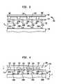
- FIG. 3is a diagrammatic elevational view depicting the package of FIGS. 1-2 in conjunction with a test circuit panel during one step of a method according to one embodiment of the invention.
- FIG. 4is a view similar to FIG. 3 but depicting a later stage of the method.
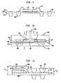
- FIG. 5is a diagrammatic, idealized perspective view depicting a portion of the package shown in FIGS. 1-4 .
- FIG. 6is a fragmentary sectional view depicting a portion of an assembly including the package of FIGS. 1-5 .
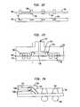
- FIG. 7Ashows a front elevational view of a testing assembly during a method of testing a microelectronic element, in accordance with one preferred embodiment of the present invention.
- FIG. 7Bshows the testing assembly of FIG. 7A during a later stage of testing the microelectronic element.
- FIG. 8shows a cross-sectional view of an assembly for testing microelectronic elements, in accordance with still further preferred embodiments of the present invention.
- FIG. 9shows a front elevational view of a microelectronic package, in accordance with another preferred embodiment of the present invention.
- FIG. 10shows the package of FIG. 9 after the package has been placed in a mold, in accordance with certain preferred embodiments of the present invention.
- FIG. 11shows the package of FIGS. 9 and 10 after an overmold has been formed on the package, in accordance with certain preferred embodiments of the present invention.
- FIG. 12shows another view of the package shown in FIG. 11 .
- FIG. 13shows a stack of microelectronic packages, in accordance with certain preferred embodiments of the present invention.
- FIG. 14shows a top plate of a mold for making a microelectronic package, in accordance with certain preferred embodiments of the present invention.
- FIG. 15shows a microelectronic package and a mold for forming an overmold on the package, in accordance with certain preferred embodiments of the present invention.
- FIG. 16shows a partial front elevational view of a microelectronic package having an overmold, in accordance with certain preferred embodiments of the present invention.
- FIG. 17shows the package of FIG. 16 in a stacked assembly.
- FIGS. 18 and 19show a mold for compressing conductive elements on a microelectronic package, in accordance with certain preferred embodiments of the present invention
- FIG. 20shows a partial view of a microelectronic package, in accordance with certain preferred embodiments of the present invention.
- FIG. 21shows the package of FIG. 20 in a stacked assembly.
- FIGS. 22-24show a method of making a microelectronic package, in accordance with another preferred embodiment of the present invention.
- FIG. 25shows a microelectronic package, in accordance with another preferred embodiment of the present invention.
- FIG. 26shows the package of FIG. 25 in a stacked assembly.
- FIGS. 27-32show a method of making a microelectronic package, in accordance with certain preferred embodiments of the present invention.
- FIG. 33shows a top plan view of the microelectronic package shown in FIG. 30 .
- FIG. 34shows another view of the package shown in FIG. 32 .
- FIG. 35shows the package of FIG. 34 in a stacked assembly.
- FIG. 36shows an X-ray image of a section of the package shown in FIG. 34 .
- FIGS. 37Ashows a cross-sectional view of a section of the package shown in FIG. 34 .
- FIG. 37Bshows a magnified view of a section of the package shown in FIG. 34 .
- FIG. 38shows a microelectronic package, in accordance with another preferred embodiment of the present invention.
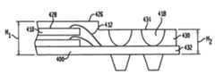
- a microelectronic package 100includes a microelectronic element, such as a semiconductor chip 102 , having a front or contact bearing face 104 and electrical contacts 106 exposed at face 104 .
- a passivation layer 108may be formed over the contact bearing face 104 with openings at contacts 106 .
- the microelectronic package 100also includes conductive support elements 110 such as solder balls in substantial alignment and electrically interconnected with contacts 106 .
- contacts 106 and support elements 110are disposed in an array which in this case is a rectilinear grid, having equally spaced columns extending in a first horizontal direction x and equally spaced rows extending in a second horizontal direction y orthogonal to the first horizontal direction.
- Each contact 106 and support element 110is disposed at an intersection of a row and a column, so that each set of four support elements 110 at adjacent intersections, such as support elements 110 a , 110 b , 110 c and 110 d , defines a generally rectangular, and preferably square, zone 112 .
- the directions referred to in this disclosureare directions in the frame of reference of the components themselves, rather than in the normal gravitational frame of reference.
- Horizontal directionsare directions parallel to the plane of the front surface 104 of the chip, whereas vertical directions are perpendicular to that plane.
- the packagealso includes a flexible dielectric substrate 114 , such as a polyimide or other polymeric sheet, including a top surface 116 and a bottom surface 118 remote therefrom.
- a flexible dielectric substrate 114such as a polyimide or other polymeric sheet, including a top surface 116 and a bottom surface 118 remote therefrom.
- the flexible sheet 114has conductive traces 120 thereon. In the particular embodiment illustrated in FIG. 1 , the conductive traces are disposed on the bottom surface 118 of the flexible sheet 114 . In other preferred embodiments, however, the conductive traces 120 may extend on the top surface 116 of the flexible sheet 114 , on both the top and bottom faces or within the interior of the flexible substrate 114 .
- Conductive traces 96may be formed from any electrically conductive material, but most typically are formed from copper, copper alloys, gold or combinations of these materials. The thickness of the traces will also vary with the application, but typically is about 5 ⁇ m-25 ⁇ m. Traces 120 are arranged so that each trace has a support end 122 and a post end 124 remote from the support end.
- Each post 126is connected to the post end 124 of one of the traces 120 .
- the posts 126extend upwardly through the dielectric sheet 114 , from the post ends of the traces.
- the dimensions of the postscan vary over a significant range, but most typically the height h p of each post above the top surface 116 of the flexible sheet is about 50-300 ⁇ m.
- Each posthas a base 128 adjacent the flexible sheet 114 and a tip 130 remote from the flexible sheet.
- the postsare generally frustoconical, so that the base 128 and tip 130 of each post are substantially circular.
- the bases of the poststypically are about 100-600 ⁇ m in diameter, whereas the tips typically are about 40-200 ⁇ m in diameter.
- the postsmay be formed from any electrically conductive material, but desirably are formed from metallic materials such as copper, copper alloys, gold and combinations thereof.
- the postsmay be formed principally from copper with a layer of gold at the surfaces of the posts.
- the dielectric sheet 114 , traces 120 and posts 126can be fabricated by a process such as that disclosed in co-pending, commonly assigned U.S. Provisional Patent Application Ser. No. 60/508,970, the disclosure of which is incorporated by reference herein.
- a metallic plateis etched or otherwise treated to form numerous metallic posts projecting from the plate.
- a dielectric layeris applied to this plate so that the posts project through the dielectric layer.
- An inner or side of the dielectric layerfaces toward the metallic plate, whereas the outer side of the dielectric layer faces towards the tips of the posts.
- the dielectric layermay be fabricated by coating a dielectric such as polyimide onto the plate around the posts or, more typically, by forcibly engaging the posts with the dielectric sheet so that the posts penetrate through the sheet. Once the sheet is in place, the metallic plate is etched to form individual traces on the inner side of the dielectric layer.
- conventional processessuch as plating may form the traces or etching, whereas the posts may be formed using the methods disclosed in commonly assigned U.S. Pat. No. 6,177,636, the disclosure of which is hereby incorporated by reference herein.
- the postsmay be fabricated as individual elements and assembled to the flexible sheet in any suitable manner, which connects the posts to the traces.
- the support ends 122 of the leadsare disposed in a regular grid pattern corresponding to the grid pattern of the support elements, whereas the posts 126 are disposed in a similar grid pattern.
- the grid pattern of the postsis offset in the first and second horizontal directions x and y from the grid pattern of the support ends 122 and support elements 110 , so that each post 126 is offset in the ⁇ y and +x directions from the support end 122 of the trace 120 connected to that post.
- each trace 120overlies a support element 110 and is bonded to such support element, so that each post 126 is connected to one support element.
- the bondscan be made by providing the support elements on the contacts 106 of the chip and positioning the substrate or flexible sheet 114 , with the posts and traces already formed thereon, over the support elements and reflowing the solder balls by heating the assembly.
- the solder ballscan be provided on the support ends 122 of the traces.
- the process steps used to connect the support ends of the tracescan be essentially the same used in flip-chip solder bonding of a chip to a circuit panel.
- the posts 126are offset from the support elements 110 in the x and y horizontal directions.
- the offset distance d o ( FIG. 2 ) between a post and a support elementcan be taken as the distance between the center of area of the base 128 ( FIG. 1 ) of the post and the center of area of the upper end 132 ( FIG. 1 ) of the support element 110 .
- the centers of arealie at the geometric centers of these elements.
- the offset distance d ois large enough that there is a gap 134 ( FIG. 2 ) between adjacent edges of the base of the post and the top end of the support element. Stated another way, there is a portion of the dielectric sheet 114 in gap 134 , which is not in contact with either the top end 132 of the support element or the base 128 of the post.
- Each postlies near the center of one zone 112 defined by four adjacent support elements 110 , so that these support elements are disposed around the post.
- support elements 110 a - 110 dare disposed around post 126 A.
- Each postis electrically connected by a trace and by one of these adjacent support elements to the microelectronic device 102 .
- the offset distances from a particular post to all of the support elements adjacent to that postmay be equal or unequal to one another.
- the upper surface 116 of the substrate or flexible sheet 114forms an exposed surface of the package, whereas posts 126 project from this exposed surface and provide terminals for connection to external elements
- the conductive support elements 110create electrically conductive paths between the microelectronic element 102 and the flexible substrate 114 and traces 120 .
- the conductive support elementsspace the flexible substrate 114 from the contact bearing face 104 of microelectronic element 102 . As further discussed below, this arrangement facilitates movement of the posts 126 .
- a microelectronic package 100such as the package discussed above with reference to FIGS. 1 and 2 is tested by juxtaposing the conductive posts 126 with contact pads 136 on a second microelectronic element 138 such as a circuitized test board.
- the conductive posts 126 A- 126 Dare placed in substantial alignment with top surfaces of the respective contact pads 136 A- 136 D.
- the top surfaces 140 A- 140 D of the respective contact pads 136 A- 136 Dare disposed at different heights and do not lie in the same plane.
- Such non-planaritycan arise from causes such as warpage of the circuit board 138 itself and unequal thicknesses of contact pads 136 .
- the tips 130 of the postsmay not be precisely coplanar with one another, due to factors such as unequal heights of support elements 110 ; non-planarity of the front surface 104 of the microelectronic device; warpage of the dielectric substrate 114 ; and unequal heights of the posts themselves.
- the package 100may be tilted slightly with respect to the circuit board. For these and other reasons, the vertical distances Dv between the tips of the posts and the contact pads may be unequal.
- the microelectronic package 100is moved toward the test board 138 , by moving the test board, the package or both.
- the tips 130 of the conductive posts 126 A- 126 Dengage the contact pads 136 and make electrical contact with the contact pads.
- the tips of the postsare able to move so as to compensate for the initial differences in vertical spacing Dv ( FIG. 3 ), so that all of the tips can be brought into contact with all of the contact pads simultaneously using only a moderate vertical force applied to urge the package and test board 138 together.
- at least some of the post tipsare displaced in the vertical or z direction relative to other post tips.
- a significant portion of this relative displacementarises from movement of the bases 128 of the posts relative to one another and relative to microelectronic element 100 . Because the posts are attached to flexible substrate 114 and are offset from the support elements 110 , and because the support elements space the flexible substrate 114 from the front surface 104 of the microelectronic element, the flexible substrate can deform. Further, different portions of the substrate associated with different posts can deform independently of one another.
- FIG. 5An idealized representation of the deformation of a single region 112 of substrate 114 is shown in FIG. 5 .
- the support elements 110 disposed at the corners of the regionallow the central part of the region to bend downwardly toward the microelectronic element 102 , allowing the base 128 of post 126 to also move downward toward the microelectronic element.
- This deformationis idealized in FIG. 5 as a pure displacement of the post and the center of the region in the vertical or z direction.
- the deformation of the substratemay include bending and/or stretching of the substrate so that the motion of the base may include a tilting about an axis in the x-y or horizontal plane as well as some horizontal displacement of the base, and may also include other components of motion.
- one portion of the regionmay be reinforced by a trace, and will tend to be stiffer than the other portions of the region.
- a particular postmay be positioned off-center in its region 112 , so that the post lies closer to one support element, or to a pair of support elements, on one side of the post.
- post 126 aFIG. 2
- post 126 amay be disposed closer to support elements 110 a and 110 b than to support elements 110 c and 110 d .
- the relatively small portion of the substrate between the post and support elements 110 a and 110 bwill be stiffer in bending than the relatively large portion of the substrate between the posts and support elements 110 c and 110 d .
- Such non-uniformitiestend to promote non-uniform bending and hence tilting motion of the posts. Tilting of the posts tends to move the tips 130 toward the microelectronic element.
- the support elements 110 at the corners of the individual regionssubstantially isolate the various regions from one another, so that the deformation of each region is substantially independent of the deformation of other regions of the substrate 114 .
- the posts 126themselves may also flex or buckle to some degree, which provides additional movement of tips 76 in the vertical or z direction.
- the independent displacement of the posts relative to one anotherallows all of the post tips 130 to contact all of the contact pads 136 on the test substrate.
- the flexible substrate 114 in the vicinity of conductive post 126 Cflexes substantially more than the flexible substrate in the vicinity of conductive post 126 B.
- the flexible substrate 114 in the vicinity of conductive post 126 Bflexes substantially more than the flexible substrate in the vicinity of conductive post 126 A.
- the packagecan be tested reliably by applying test signals, power and ground potentials through the test circuit board 138 and through the engaged posts and contact pads. Moreover, this reliable engagement is achieved with a simple test circuit board 138 .
- the contact pads 136 of the test circuit boardare simple, planar pads.
- the test circuit boardneed not incorporate special features to compensate for non-planarity or complex socket configurations.
- the test circuit boardcan be made using the techniques commonly employed to form ordinary circuit boards. This materially reduces the cost of the test circuit board, and also facilitates construction of the test circuit board with traces (not shown) in a simple layout compatible with high-frequency signals.
- the test circuit boardmay incorporate electronic elements such as capacitors in close proximity to the contact pads as required for certain high-frequency signal processing circuits.
- electronic elementssuch as capacitors in close proximity to the contact pads as required for certain high-frequency signal processing circuits.
- the test circuit boardneed not incorporate special features to accommodate non-planarity, placement of such electronic elements is simplified.
- the internal features of package 100are also compatible with high-frequency signals.
- the conductive support elements, traces and postsprovide low-impedance signal paths between the tips of the posts and the contacts 106 of the microelectronic element. Because each post 126 is connected to an immediately adjacent conductive support element 110 , traces 120 are quite short.
- the low-impedance signal pathsare particularly useful in high-frequency operation, as, for example, where the microelectronic element must send or receive signals at a frequency of 300 MHz or more.
- the microelectronic package 100may be removed from the test circuit board 138 and permanently interconnected with another substrate such as a circuit panel 140 ( FIG. 6 ) having contact pads 142 , as by bonding the tips 130 of posts 126 to the contact pads of the circuit panel using a conductive bonding material 144 such as a solder.
- the solder-bonding processmay be performed using conventional equipment commonly used for surface-mounting microelectronic components.
- the solder massesmay be provided on the posts 126 or on the contact pads 142 , and may be reflowed after engaging the posts with the contact pads. During reflow, the surface tension of the solder tends to center the posts on the contact pads.
- Such self-centering actionis particularly pronounced where the tips of the posts are smaller than the contact pads.
- the solder 144wets the sides of the posts to at least some extent, and thus forms a fillet encircling the tip of each post, as well as a strong bond between the confronting surfaces of the posts and pads.
- the tips 130 of the posts 126can move relative to the microelectronic element 102 to at least some degree during service so as to relieve stresses arising from differential thermal expansion and contraction.
- the individual posts 126can move relative to the microelectronic element and relative to the other posts by flexure or other deformation of substrate 114 . Such movement can appreciably relieve stresses in the solder bonds between the posts and the contact pads, which would otherwise occur upon differential thermal expansion or contraction of the circuit board 140 and microelectronic element 102 .
- the conductive support elements or solder balls 110can deform to further relieve stresses in solder masses 144 .
- the assemblyis highly resistant to thermal cycling stresses, and hence highly reliable in service.
- An underfill materialsuch as an epoxy or other polymeric material may be provided around the tips of the posts and around the contact pads, so as to reinforce the solder bonds. Desirably, this underfill material only partially fills the gap between the package 100 and the circuit board 140 . In this arrangement, the underfill does not bond the flexible substrate 114 or the microelectronic device to the circuit board. The underfill only reinforces the posts at their joints with the contact pads. However, no reinforcement is required at the bases of the posts, inasmuch as the joint between the base of each post and the associated trace is extraordinarily resistant to fatigue failure.
- the assemblyis also compact. Some or all of the posts 126 and contact pads 142 are disposed in the area occupied by the microelectronic element 102 , so that the area of circuit board 140 occupied by the assembly may be equal to, or only slightly larger than, the area of the microelectronic element itself, i.e., the area of the front surface 104 of the microelectronic element 100 .
- the packagemay include more than one microelectronic element or more than one substrate.
- the process steps used to assemble the flexible substrate, support elements and posts to the chipsmay be performed while the chips are in the form of a wafer.
- a single large substratemay be assembled to an entire wafer, or to some portion of the wafer.
- the assemblymay be severed so as to form individual units, each including one or more of the chips and the associated portion of the substrate.
- the testing operations discussed abovemay be performed prior to the severing step.
- the ability of the packages to compensate for non-planarity in a test board or in the wafer itselfgreatly facilitates testing of a large unit.
- the substrate and tracesmay deform locally in regions surrounding the posts. These regions tend to deform upwardly, leaving concavities in the bottom surface of the substrate.
- the postsmay have heads, and these heads may be lodged partially or completely within the concavities.
- the top surface of the substratemay be abutted against a die having holes aligned with locations where posts are forced through the substrate. Such a die can also help to prevent delamination of the substrate and traces.
- the tracesmay be disposed on the top or bottom surface of a single-layer substrate.
- the resulting post-array substratecan be assembled with a microelectronic element to form a package as discussed above, or can be used in any other microelectronic assembly where a small post array is desirable.
- the assembly processallows selective placement of posts. It is not essential to provide the lands and holes in the traces. Thus, posts can be placed at any location along any trace.
- the postsmay be formed from essentially any conductive material. Different posts may be formed from different materials. For example, posts subject to severe mechanical loading can be formed entirely or partially from hard refractory metals such as tungsten, while other posts may be formed from softer metals such as copper. Also, some or all of the posts may be formed entirely or partially from corrosion-resistant metals such as nickel, gold or platinum.
- the dielectric sheet, traces and postsmay be fabricated by a process such as that disclosed in co-pending, commonly assigned U.S. Provisional Patent Application Ser. No. 60/508,970, the disclosure of which is hereby incorporated by reference herein.
- a metallic plateis etched or otherwise treated to form numerous metallic posts projecting from the plate.
- a dielectric layeris applied to this plate so that the posts project through the dielectric layer.
- An inner face of the dielectric layerfaces toward the metallic plate, whereas the outer face of the dielectric layer faces towards the tips of the posts.
- the dielectric layermay be fabricated by coating a dielectric such as polyimide onto the plate around the posts or, more typically, by forcibly engaging the posts with the dielectric sheet so that the posts penetrate through the sheet. Once the sheet is in place, the metallic plate is etched to form individual traces on the inner side of the dielectric layer.
- conventional processessuch as plating may form the traces or etching, whereas the posts may be formed using the methods disclosed in commonly assigned U.S. Pat. No. 6,177,636, the disclosure of which is hereby incorporated by reference herein.
- the postsmay be fabricated as individual elements and assembled to the flexible sheet in any suitable manner, which connects the posts to the traces.
- the upper surface of the substrate or flexible sheetforms an exposed surface of the package, whereas posts project from this exposed surface and provide terminals for connection to external elements.
- FIGS. 7A and 7Bshow a method of testing a microelectronic element 260 using a testing assembly 220 .
- the microelectronic element 260such as a semiconductor chip, has a front face 262 including contacts 264 accessible at the front face and a rear face 266 remote therefrom.
- the contacts 264 of the microelectronic elementare juxtaposed with the conductive posts 246 of the test board 222 .
- the contacts 264 A- 264 Dare placed in substantial alignment with top surfaces 250 of the respective conductive posts 246 A- 246 D.
- the top surfaces 266 A- 266 D of the respective contact pads 264 A- 264 Dare disposed at different heights and do not lie in the same plane. Such non-planarity can arise from causes such as warpage of the microelectronic element 260 itself and unequal thicknesses of contact pads 264 .
- the tips 250 of the posts 246may not be precisely coplanar with one another, due to factors such as unequal heights of support elements 230 ; non-planarity of the first surface 224 of the test board 222 ; warpage of the dielectric substrate 232 ; and unequal heights of the posts themselves.
- the microelectronic element 260may be tilted slightly with respect to the test board. For these and other reasons, the vertical distances Dv between the contacts 264 and the tips of the posts 246 may be unequal.
- the microelectronic element 260is moved toward the test board 222 , by moving the test board, the microelectronic element or both toward one another.
- the contacts 264engage the conductive posts 246 A- 246 D for making electrical contact with the conductive posts.
- the tips 250 of the posts 246 A- 246 Dare able to move so as to compensate for the initial differences in vertical spacing Dv ( FIG. 7A ), so that all of the tips can be brought into contact with all of the contact pads simultaneously using with only a moderate vertical force applied to urge the microelectronic element 260 and the test board 222 together. In this process, at least some of the post tips 246 A- 246 D are displaced in the vertical or z direction relative to others of the post tips.
- a significant portion of this relative displacementarises from movement of the bases 248 of the posts relative to one another and relative to test board 220 .
- the postsare attached to flexible substrate 232 and are offset from the support elements 230 , and because the support elements space the flexible substrate 232 from the first surface 224 of the test board, the flexible substrate 232 can deform. Further, different portions of the substrate associated with different posts can deform independently of one another.
- the support elements 230allow region 268 of flexible substrate 232 to bend downwardly toward the test board 222 , allowing the base 248 of post 246 B to also move downward toward the test board. This deformation is idealized in FIG.
- the deformation of the substrate 232may include bending and/or stretching of the substrate so that the motion of the base may include a tilting about an axis in the x-y or horizontal plane as well as some horizontal displacement of the base, and may also include other components of motion.
- one portion of the regionmay be reinforced by a conductive trace (not shown), which will tend to be stiffer than the other portions of the region.
- a particular postmay be positioned off-center in its region 268 , so that the post lies closer to one support element 230 , or to a pair of support elements, on one side of the post.
- post 246 amay be disposed closer to support elements 230 a and 230 b than to support elements 230 c and 230 d .
- the relatively small portion of the substrate between the post and support elements 230 a and 230 bwill be stiffer in bending than the relatively large portion of the substrate between the posts and support elements 230 c and 230 d .
- Such non-uniformitiestend to promote non-uniform bending and hence tilting motion of the posts. Tilting of the posts tends to move the tips 250 toward the test board 222 .
- the support elements 230 at the corners of the individual regionssubstantially isolate the various regions from one another, so that the deformation of each region is substantially independent of the deformation of other regions of the flexible, dielectric substrate 232 .
- the posts 246themselves may also flex or buckle to some degree, which provides additional movement of tips 250 in the vertical or z direction.
- the independent displacement of the posts 246 relative to one anotherallows all of the contacts 264 of the microelectronic element 260 to contact all of the post tips 250 on the test board 222 .
- the flexible substrate 232 in the vicinity of conductive post 246 Bflexes substantially more than the flexible substrate in the vicinity of conductive post 246 C.
- the flexible substrate 232 in the vicinity of conductive post 246 Cflexes substantially more than the flexible substrate in the vicinity of conductive post 246 D.
- the microelectronic element 260can be tested reliably by applying test signals, power and ground potentials through the test board 222 and through the engaged contacts and posts.
- the test circuit boardcan be made using the techniques commonly employed to form ordinary circuit boards.
- the test circuit boardmay incorporate electronic elements such as capacitors in close proximity to the contact pads as required for certain high-frequency signal processing circuits.
- the internal features of the microelectronic element 260are also compatible with high-frequency signals.
- the conductive support elements 230 , traces 238 and posts 246provide low-impedance signal paths between the tips 250 of the posts and the contacts 264 of the microelectronic element 260 . Because each post 246 is connected to an immediately adjacent conductive support element 230 , traces 238 may be quite short.
- the low-impedance signal pathsare particularly useful in high-frequency operation, as, for example, where the microelectronic element must send or receive signals at a frequency of 300 MHz or more.
- the microelectronic element 260may be removed from the testing assembly 220 and packaged using an interposer such as a circuitized, dielectric film.
- the microelectronic packagesuch as a ball grid array package, may be connected with contact pads on a circuit panel using a conductive bonding material such as solder.
- the solder-bonding processmay be performed using conventional equipment commonly used for surface-mounting microelectronic components.
- the solder massesmay be provided on the terminals of the microelectronic package, and may be reflowed after engaging the terminals with the conductive pads.
- a testing assembly 320has a compliant material 370 positioned between a flexible substrate 332 and a test board 322 .
- the compliant material layer 370preferably does not substantially restrict movement of conductive posts 346 .
- the compliant materialdesirably prevents contaminants from entering the testing assembly 320 .
- the compliant material 370may be a gel, foam or the like.
- conductive elements 330still support the flexible substrate 332 to a substantial degree.
- the conductive postsare free to move independently of other conductive posts so as to ensure reliable contact between each conductive post and each conductive pad on a test board.
- the tips of the conductive postsare able to move so as to compensate for potential differences in vertical spacing so that all of the tips can be brought into contact with all of the conductive pads simultaneously using with only a moderate vertical force applied to urge a testable package and a test board together.
- at least some of the tips of the conductive postsare displaced in the vertical or z direction relative to others of the post tips.
- different portions of the flexible substrate associated with different conductive postscan deform independently of one another.
- the deformation of the substratemay include bending and/or stretching of the substrate so that the motion of the base may include a tilting about an axis in the x-y or horizontal plane as well as some horizontal displacement of the base, and may also include other components of motion.
- the dimensions of the conductive postscan vary over a significant range, but most typically the height of each post above the surface of the dielectric substrate is about 50-300 ⁇ m.
- Each posthas a base adjacent the dielectric substrate and a tip remote from the dielectric substrate.
- the postsare generally frustoconical, so that the base and tip of each post are substantially circular.
- the bases of the poststypically are about 100-600 ⁇ m in diameter, whereas the tips typically are about 40-200 ⁇ m in diameter.
- the postsmay be formed from any electrically conductive material, but desirably are formed from metallic materials such as copper, copper alloys, gold and combinations thereof.
- the postsmay be formed principally from copper with a layer of gold at the surfaces of the posts.
- the conductive tracesare disposed on a bottom surface of the dielectric layer.
- the conductive tracesmay extend on the top surface of the dielectric layer; on both the top and bottom faces or within the interior of the dielectric layer.
- a statement that a first feature is disposed “on” a second featureshould not be understood as requiring that the first feature lie on a surface of the second feature.
- the conductive tracesmay be formed from any electrically conductive material, but most typically are formed from copper, copper alloys, gold or combinations of these materials. The thickness of the traces will also vary with the application, but typically is about 5 ⁇ m-25 ⁇ m.
- the tips of the postsmay not be precisely coplanar with one another, due to factors such as non-planarity of the front surface of the microelectronic device; warpage of the dielectric substrate; and unequal heights of the posts themselves. Also, the package may be tilted slightly with respect to the circuit board. For these and other reasons, the vertical distances between the tips of the posts and the contact pads may be unequal. The independent displacement of the posts relative to one another allows all of the post tips to contact all of the contact pads on the test substrate.
- the packagecan be tested reliably by applying test signals, power and ground potentials through the test circuit board and through the engaged posts and contact pads. Moreover, this reliable engagement is achieved with a simple test circuit board.
- the contact pads of the test circuit boardare simple, planar pads.
- the test circuit boardneed not incorporate special features to compensate for non-planarity or complex socket configurations.
- the test circuit boardcan be made using the techniques commonly employed to form ordinary circuit boards. This materially reduces the cost of the test circuit board, and also facilitates construction of the test circuit board with traces (not shown) in a simple layout compatible with high-frequency signals.
- the test circuit boardmay incorporate electronic elements such as capacitors in close proximity to the contact pads as required for certain high-frequency signal processing circuits.
- electronic elementssuch as capacitors in close proximity to the contact pads as required for certain high-frequency signal processing circuits.
- the test circuit boardneed not incorporate special features to accommodate non-planarity, placement of such electronic elements is simplified.
- a particle coatingsuch as that disclosed in U.S. Pat. Nos. 4,804,132 and 5,083,697, the disclosures of which are incorporated by reference herein, may be provided on one or more electrically conductive parts of a microelectronic package for enhancing the formation of electrical interconnections between microelectronic elements and for facilitating testing of microelectronic packages.
- the particle coatingis preferably provided over conductive parts such as conductive terminals or the tip ends of conductive posts.
- the particle coatingis a metalized diamond crystal coating that is selectively electroplated onto the conductive parts of a microelectronic element using standard photoresist techniques.
- a conductive part with the diamond crystal coatingmay be pressed onto an opposing contact pad for piercing the oxidation layer present at the outer surface of the contact pad.
- the diamond crystal coatingfacilitates the formation of reliable -electrical interconnections through penetration of oxide layers, in addition to traditional wiping action.
- the motion of the postsmay include a tilting motion. This tilting motion causes the tip of each post to wipe across the contact pad as the tip is engaged with the contact pad. This promotes reliable electrical contact.
- the postsmay be provided with features which promote such wiping action and otherwise facilitate engagement of the posts and contacts.
- the flexible substratemay be provided with features to enhance the ability of the posts to move independently of one another and which enhance the tilting and wiping action.
- a microelectronic packageincludes a substrate 400 having a first or top surface 402 and a second or bottom surface 404 .
- the substrateincludes conductive pads 406 accessible at the top surface 402 and conductive posts 408 projecting from the second surface 404 of the substrate 400 .
- the substrate 400may be flexible and may be made of a dielectric material such as polyimide.
- the substratemay also have conductive traces (not shown) that extend over the top surface 402 , the bottom surface 404 and/or between the top and bottom surfaces.
- a microelectronic element 410such as a semiconductor chip is attached to the first surface 402 with a flexible substrate 400 .
- the microelectronic elementis electrically interconnected with one or more of the conductive pads 406 using conductive elements 412 such as wire bonds.
- An adhesive 414is preferably used for attaching the microelectronic element 410 to the substrate 400 .
- the substrate 400may be placed onto a bottom plate 416 of a mold.
- the bottom plate 416preferably includes a top surface having recesses that are adapted to receive the conductive posts 408 .
- the recessesmay have a shape that generally mirrors the shape of the posts.
- conductive masses 418such as elongated conductive elements or solder balls are provided atop the conductive pads 406 ( FIG. 9 ) accessible at the first surface 402 of the flexible substrate 400 .
- a top plate 420 of the moldis then positioned over the bottom plate 416 of the mold for capturing the flexible substrate 400 therebetween.
- the top plate 420 of the moldis placed in contact with the first surface 402 of the flexible substrate and the bottom plate 416 of the mold is in contact with the second surface 404 of the flexible substrate 400 .
- the mold top plate 420includes an inlet 422 that enables a flowable material to be introduced into a cavity 424 defined by the mold bottom plate 416 and the mold top plate 420 .
- the bottom plate 416 and the top plate 420 of the moldare preferably pressed together to form an air-tight seal at the periphery thereof.
- the conductive masses 418are planarized so that the top surfaces of the conductive masses lie in a common plane and are the same height above the top surface of the chip 410 .
- the tips of the conductive posts 408are also planarized so that the tips lie in a common plane and are all at the same vertical distance relative to the top surface of the chip 410 .
- the planarization of the conductive masses 418 and the conductive posts 408will provide packages having uniform vertical heights across the horizontal width thereof.
- a plurality of packagesmay be produced, with each package having a substantially identical vertical height. As a result, microelectronic packages having the exact same vertical dimensions may be quickly and reliably produced.
- a curable, flowable materialsuch as a curable encapsulant is introduced into the cavity 424 of the mold through the inlet 422 .
- the curable encapsulantmay be clear, opaque or have optical properties anywhere along the scale between clear and opaque.
- the encapsulantmay be clear when the microelectronic element 410 is an LED or optically-sensitive chip.
- the curable materialis preferably cured to form a cured encapsulant layer, which preferably provides stability to the package and protects the microelectronic element 410 , the conductive wires 414 and the conductive masses 418 .
- the cured encapsulant 426includes a central section 428 having a height H 1 that is sufficient to cover the semiconductor chip 410 and the wire bonds 412 .
- the encapsulant 426also includes a peripheral region 430 that extends to a peripheral edge 432 of the flexible substrate 400 .
- the encapsulant in the peripheral regionhas a height H 2 that is less than H 1 .
- the solder masses 418include top surfaces 434 that are exposed at a top surface of the peripheral portion 430 of the encapsulant 426 . In certain preferred embodiments, the accessibility of the solder masses 418 is provided by the top mold plate 420 . As shown in FIG.
- the height of the cavity 424 in the area of the solder masses 418is less than the height of the cavity overlying the chip 410 and the wire bonds 414 .
- the encapsulant 426does not cover the top surfaces of the solder masses 418 so that the solder masses are accessible at a top surface of the cured encapsulant layer 426 .
- FIG. 12shows the microelectronic package shown in FIG. 11 .
- the packageincludes the flexible substrate 400 having a first microelectronic element 410 A that is electrically interconnected with one or more of the conductive posts 408 and/or one or more of the conductive masses 418 accessible at a peripheral region of the encapsulant 426 .
- the microelectronic packagealso preferably includes a second microelectronic element 410 B that is positioned over the first microelectronic element 410 A.
- the second microelectronic element 401 Bis also electrically interconnected with one or more of the conductive posts 408 and/or one or more of the conductive masses 418 .
- a central region 428 of the encapsulant 426has a height sufficient to cover the microelectronic elements 410 A, 410 B and the conductive wires 412 used for electrically interconnecting the microelectronic elements with the substrate 400 .
- the peripheral region 430 of the encapsulanthas a lower height so that the tops of the conductive masses 418 are accessible and exposed at an exposed surface of the peripheral region 430 and hence, at an exposed surface of the package.
- the structure shown in FIG. 12provides a microelectronic package that may be stacked either on top of or below another microelectronic package.
- FIG. 13shows the microelectronic package of FIG. 12 stacked on top of another microelectronic packages.
- a first microelectronic package 400 Ais stacked atop a second microelectronic package 400 B, which is stacked atop a third microelectronic package 400 C, which is stacked atop a fourth microelectronic package 400 D.
- the four microelectronic packagesare preferably electrically interconnected with one another.
- the conductive posts 408 A-of the first microelectronic package 400 Aare in contact with the conductive masses 418 B of the second microelectronic package 400 B.
- the conductive masses 418 Bare preferably elevated in temperature so as to at least partially transform into a molten state so that the conductive posts 408 A can be at least partially inserted therein.
- the temperature of the conductive masses 418 Bmay be lowered so that the conductive masses re-solidify for permanently connecting the conductive posts 408 A and the conductive masses 418 B.
- the electrical connections between the second microelectronic package 400 B and the third microelectronic package 400 Care made in a similar fashion, as are the electrical interconnections between the third microelectronic package 400 C and the fourth microelectronic package 400 D.
- FIG. 13shows an assembly including four microelectronic packages stacked one atop the other, the present invention contemplates that any size package of two or more microelectronic packages may be manufactured.
- a stack of five or more microelectronic packagesmay be possible.
- the uppermost or lowermost package in the stackmay be connected to an external element such as a circuit board or a test board.
- each individual packageis preferably tested.
- a top plate 520 of a moldin another preferred embodiment of the present invention, includes a top surface 536 and a bottom surface 538 .
- the mold top plate 520includes an inlet 522 that extends into a cavity 524 .
- the mold top plate 520also includes one or more projections 540 that extend into the cavity 524 .
- the mold top plate 520is secured over the substrate 500 .
- the projections 540 of the mold top plate 520preferably compress the conductive masses 518 that are positioned atop the first surface of the substrate 500 .
- the conductive postsmay also be compressed. As described above, the compression of the conductive masses and/or the conductive posts serves to planarize the conductive elements so that the vertical height of the package is uniform across the package.
- a curable encapsulant materialis introduced through inlet 522 .
- the curable encapsulantcovers the microelectronic element 510 , the conductive wires 512 and the conductive masses 518 .
- the package 500may be removed from the mold.
- the encapsulant 526covers microelectronic elements 510 A, 510 B and conductive wires 512 .
- the peripheral portion 530 of the encapsulant 526has a height that is greater than the height of the conductive masses 518 .
- the conductive masses 518are recessed within the openings, the conductive masses have surfaces which are exposed and accessible at the top of the encapsulant layer 526 .
- microelectronic packages similar to the one shown in FIG. 16may be stacked atop one another to form a microelectronic stack.
- a first microelectronic package 500 Ais stacked atop a second microelectronic package 500 B.
- the conductive posts 508 A of the first microelectronic package 500 Aare in electrical contact with the conductive masses 518 B of the second microelectronic package 500 B.
- the stacked packagehas a lower overall silhouette due to the recess of the conductive masses 518 in the encapsulant layer 526 .
- FIG. 18shows a top plate 620 of a mold, in accordance with another preferred embodiment of the present invention.
- the top plate 620includes a cavity having depressions 640 formed therein that are preferably provided in the same locations as the projections 540 shown in the FIG. 14 embodiment.
- FIG. 19as the conductive masses are compresssed by the mold, the conductive masses 618 extend into the recesses 640 .
- the encapsulant 626is introduced into the mold, the upper ends of the conductive masses project above the top surface 642 of the encapsulant 626 .
- the encapsulant 626may be cured and the package 600 removed from the mold. Due to the recesses 640 in the top plate 620 of the mold ( FIG. 18 ), the upper ends of the conductive masses 618 project above the top surface 642 of the encapsulant 626 .
- two or more of the microelectronic packages 600 A, 600 B shown in FIG. 20may be stacked atop one another to form a microelectronic stack.
- the conductive posts 608 A of the first microelectronic package 600 Aare in contact with the conductive masses 618 B of the second microelectronic package 600 B for forming the electrical interconnection.
- the conductive masses 618are preferably transformed into an at least partially molten state so that the conductive post 608 may be inserted therein. After the temporary connection has been made, the conductive masses may be transformed back into a solid state for forming a permanent connection between the conductive posts and the conductive masses.
- FIG. 21only two microelectronic packages are shown in FIG. 21 , it is contemplated that the present invention will enable three, four or more microelectronic packages to be stacked atop one another.
- a microelectronic packageincludes a substrate 700 , such as a flexible substrate made of a dielectric material, having a first surface 702 and a second surface 704 .
- the packageincludes conductive posts 708 projecting from the first surface 702 and conductive pads 706 accessible at the second surface 704 .
- the flexible substrateis juxtaposed with a bottom plate 716 of a mold having recesses 717 formed therein.
- a conductive mass 718such as a solder ball, is placed in each of the recesses 717 of the bottom plate 716 .
- the substrate 700is preferably placed in contact with the bottom plate 716 so that each of the conductive pads 706 is in contact with one of the conductive masses 718 .
- a top plate 720 of a moldis preferably placed over the microelectronic package and the bottom plate 716 of the mold.
- the substrate 700 of the microelectronic packageis preferably sandwiched between the mold bottom plate 716 and the mold top plate 720 .
- the moldis compressed for planarizing the tips of the conductive posts 708 and the bottoms of the conductive masses 718 .
- the moldmay be heated for transforming the conductive masses 718 to an at least partially molten state for wetting the conductive masses to the conductive pads 706 .
- a curable encapsulant materialmay be introduced through an inlet 722 of the top plate 720 .
- the curable encapsulant materialpreferably enters the cavity 724 and covers the microelectronic element 710 , the conductive wire 712 and surrounds the conductive posts 708 , with the tips of the posts being accessible and exposed at an upper surface of the encapsulant layer.
- the curable liquid encapsulantis preferably cured to provide the microelectronic package shown in FIG. 24 .
- the encapsulant layermay be rigid, at least partially rigid or compliant.
- the encapsulant 726preferably has a central region 728 that covers the microelectronic elements 710 A, 710 B and the conductive wires 712 .
- the tips of the conductive posts 708are preferably accessible through the encapsulant at a peripheral region 730 of the encapsulant 726 .
- the conductive masses 718are accessible at a bottom of the microelectronic package.
- FIG. 25shows another view of the microelectronic package shown in FIG. 24 .
- the microelectronic packageincludes substrate 700 having a first surface 702 and a second surface 704 remote therefrom.
- the packageincludes a first microelectronic element 710 A overlying a second microelectronic element 710 B.
- the microelectronic elementsare electrically interconnected with the substrate using conductive wires 712 .
- the packageincludes encapsulant layer 726 having a central region 728 having a height H 1 and a peripheral region 730 having a lower height H 2 .
- the height H 1 of the central region 728is sufficient to cover the microelectronic elements 710 A, 710 B and the wire bond 712 .
- the lower height H 2 of the peripheral region 730enables the tips of the conductive posts 708 to be accessible therethrough and have portions which are exposed at an exposed surface of the peripheral region 730 of the encapsulant layer, and hence, at an exposed surface of the package.
- the structure shown in FIG. 25provides a microelectronic package having conductive elements, such as conductive posts, accessible and having portions exposed at a top surface thereof and second conductive elements, such as solder balls, accessible at a bottom surface thereof.
- the microelectronic packagemay be stacked with one or more other microelectronic packages.
- the packagemay have first conductive posts accessible at a top of the package and second conductive posts accessible at a bottom of the package for stacking.
- FIG. 26shows the microelectronic package of FIG. 25 being stacked atop similarly designed microelectronic packages.
- a first microelectronic package 700 Ais stacked atop a second microelectronic package 700 B, which is stacked atop a third microelectronic package 700 C, which is stacked atop a fourth microelectronic package 700 D.
- the electrical interconnectionsare formed between the first and second packages by the conductive masses 718 A being in contact with the tips of the conductive posts 708 B of the second microelectronic package 700 B.
- the embodiment shown in FIG. 26shows four microelectronic packages being stacked one atop the other, but it is contemplated that other embodiments may include two, three, four or more microelectronic packages stacked one atop another.
- a microelectronic packageincludes a substrate 800 , such as a flexible, circuitized substrate, having a first surface 802 and a second surface 804 .
- Conductive masses 818such as solder, are placed atop the first surface 802 and conductive pads 806 are accessible at the second surface 804 . At least some of the conductive masses 818 are preferably in electrical connection with at least some of the conductive pads 806 .
- a microelectronic element 810such as a semiconductor chip is attached to the first surface 802 of the substrate 800 .
- the microelectronic element 810is electrically interconnected with one or more of the conductive masses 818 and one or more of the conductive pads 806 via wire bonds 812 .
- the microelectronic packageis placed in a mold including a bottom plate 816 and a top plate 820 having an inlet 822 .
- the flexible substrate 800is preferably sandwiched between the bottom plate 816 and the top plate 820 .
- the moldincludes a cavity 824 extending between the top plate 820 and the bottom plate 816 .
- an underside of the top plate 820at least partially compresses or collapses the conductive masses 818 .
- top surfaces of the compressed conductive massesare preferably planarized so that they lie in a common plane.
- a curable encapsulantis preferably introduced into the cavity 824 through an inlet 822 .
- the curable encapsulantpreferably covers the microelectronic element 810 , the conductive wires 812 , and surrounds the conductive masses 818 .
- the encapsulant 826is cured to provide an overmold, whereby the compressed conductive masses 818 have top surfaces that lie in a common plane and are exposed and accessible at a top surface of the encapsulant 826 .
- the conductive pads 806remain accessible at a bottom of the microelectronic package.
- a stencil 850 having opening 852is preferably positioned atop the encapsulant layer 826 of the microelectronic package.
- the stencil openings 852are preferably placed in substantial alignment with the conductive masses 818 exposed and accessible at the top surface of the encapsulant 826 .
- a solder paste 854may be swept over the stencil 850 so that a mass of solder paste 856 is deposited atop each conductive mass 818 . In other preferred embodiments, the solder paste 856 may be deposited atop the conductive masses without using a stencil.
- the conductive masses 818 and the solder paste 856 deposited thereonare desirably reflowed to form an elongated conductive element that projects above a top surface of the encapsulant layer 826 . As shown in FIG. 32 , a portion of the conductive element is exposed. Conductive elements 858 such as solder balls are attached to the conductive pads 806 at the bottom of the package.
- FIG. 33shows the compressed or collapsed solder balls 818 , which are accessible at a top surface of the encapsulant layer 826 .
- FIG. 34shows another view of the package of FIG. 32 including substrate 800 , microelectronic element 810 secured atop substrate 800 and conductive wires 812 for electrically interconnecting the microelectronic element 810 and the substrate 800 .
- the packageincludes encapsulant layer 826 and elongated conductive elements projecting above a top surface of the encapsulant layer.
- the elongated conductive -elementscomprise the reflowed solder balls and solder paste.
- FIG. 35shows the microelectronic package of FIG. 34 , after the package has been assembled into a microelectronic stack.
- the stackdesirably includes first microelectronic package 800 A stacked atop second microelectronic package 800 B, which is stacked atop third microelectronic package 800 C, which is stacked atop fourth microelectronic package 800 D.
- the conductive pads 806 A of the first microelectronic package 800 Aare in contact with the elongated conductive elements 857 B of the second microelectronic package 800 B.
- the conductive pad 806 Ais in contact with the portion of the elongated conductive element 857 B that projects above the top surface of the encapsulant layer 826 .
- a stackable assemblymay be formed.
- only the bottom microelectronic package 800 Dhas solder balls 858 attached to the conductive pads 806 D accessible at the second surface 804 D of the fourth package 800 D.
- FIG. 36shows an X-ray image after the elongated conductive elements 857 have been formed.
- flexible substrate 800includes first surface 802 and second surface 804 .
- solder balls 818are provided over the first surface 802 and flexible substrate 800 .
- the solder ballsare compressed by the mold for planarization and the encapsulant layer 826 is introduced into the cavity of the mold for surrounding the compressed solder balls 818 .
- a solder paste 856is preferably deposited atop each of the compressed solder balls 818 using the stencil shown and described above in FIG. 31 .
- the compressed solder balls 818 and the solder paste 856is reflowed for forming the elongated conductive element 857 .
- FIG. 37Ashows a cross-sectional view of the assembly shown in FIG. 36 .
- the microelectronic packageincludes substrate 800 with compressed solder balls 818 formed thereon and solder paste 856 deposited atop each of the compressed solder balls 818 .
- the solder balls 818 and the solder paste 856are reflowed to form the elongated conductive elements 857 .
- the top of the elongated conductive element 857extends above the top surface of the encapsulant layer 826 .
- FIG. 37Bshows a magnified view of one of the elongated conductive elements 857 shown in FIG. 37A .
- FIG. 38shows a microelectronic package in accordance with another preferred embodiment of the present invention.
- the packageincludes a substrate 900 having a top surface 902 and a bottom surface 904 remote therefrom.
- a first microelectronic element 910 Ais attached to the first surface 902 of the substrate 900 and a second microelectronic element 910 B is provided over the first microelectronic element 910 A.
- three or more microelectronic elementsmay be stacked atop the substrate 900 in a manner similar to the manner shown in FIG. 38 .
- the microelectronic elementsare electrically interconnected with the substrate using conductive wires 912 .
- the substrate 900includes first conductive pads 906 accessible at the top surface 902 of the substrate and second conductive pads 907 accessible at the second surface 904 of the substrate.
- Conductive masses 918 A, 918 Bsuch as solder balls, are provided over the respective conductive pads 906 , 907 .
- first solder balls 918 Aare provided over the conductive pads 906 accessible at the first surface 902 of the substrate and second solder balls 918 B are provided over the conductive pads 907 accessible at the second surface 904 of the substrate 900 .
- the packageis desirably placed in a mold similar to one of the molds shown and described above for at least partially compressing/collapsing both the first solder balls 918 A and the second solder balls 918 B.
- the moldmay be heated for transforming the solder balls into an at least partially molten state.
- the moldpreferably planarizes the solder balls so that the top surfaces of the first conductive masses 918 A lie in a first common plane and the bottom surfaces of the second conductive masses 918 B lie in a second common plane.
- a curable encapsulantmay be injected into the mold for covering the microelectronic chips 910 A, 910 B, the conductive wires 912 and surrounding the compressed or collapsed conductive masses 918 A, 918 B.
- the moldis preferably designed so that the top surfaces of the first set of collapsed solder balls 918 A are accessible and exposed at the top surface of the encapsulant and the bottom surfaces of the second set of solder balls 918 B are accessible and exposed at the bottom surface of the encapsulant.
- the structure shown in FIG. 38may be stacked atop other microelectronic packages to form a stacked assembly, similar to the stacked assembly shown in FIG. 35 .
- one or more of the conductive masses 918 A, 918 Bmay be replaced by a conductive post, such as the posts shown in FIG. 25 of the present application.
- a microelectronic package, assembly or stackmay include one or more features of one or more of the embodiments disclosed in U.S. application Ser. No. 10/959,465, filed Oct. 6, 2004, entitled “Formation of Circuitry With Modification of Feature Height” [TESSERA 3.0-358]; U.S. application Ser. No. 11/166,861, filed Jun. 24, 2005, entitled “Structure With Spherical Contact Pins” [TESSERA 3.0-416]; U.S. application Ser. No. 11/014,439, filed Dec. 16, 2004 [TESSERA 3.0-374], claiming priority of U.S. Provisional Application Ser. No. 60/533,210, filed Dec. 30, 2003; U.S.
Landscapes
- Engineering & Computer Science (AREA)
- Microelectronics & Electronic Packaging (AREA)
- Power Engineering (AREA)
- Physics & Mathematics (AREA)
- General Physics & Mathematics (AREA)
- Computer Hardware Design (AREA)
- Condensed Matter Physics & Semiconductors (AREA)
- Manufacturing & Machinery (AREA)
- General Engineering & Computer Science (AREA)
- Geometry (AREA)
- Testing Of Individual Semiconductor Devices (AREA)
- Internal Circuitry In Semiconductor Integrated Circuit Devices (AREA)
Abstract
Description
Claims (16)
Priority Applications (6)
| Application Number | Priority Date | Filing Date | Title |
|---|---|---|---|
| US11/318,404US8058101B2 (en) | 2005-12-23 | 2005-12-23 | Microelectronic packages and methods therefor |
| PCT/US2006/048499WO2007075727A2 (en) | 2005-12-23 | 2006-12-20 | Microelectronic packages and methods therefor |
| US12/769,930US8093697B2 (en) | 2005-12-23 | 2010-04-29 | Microelectronic packages and methods therefor |
| US13/012,949US8728865B2 (en) | 2005-12-23 | 2011-01-25 | Microelectronic packages and methods therefor |
| US14/242,279US9218988B2 (en) | 2005-12-23 | 2014-04-01 | Microelectronic packages and methods therefor |
| US14/933,225US9984901B2 (en) | 2005-12-23 | 2015-11-05 | Method for making a microelectronic assembly having conductive elements |
Applications Claiming Priority (1)
| Application Number | Priority Date | Filing Date | Title |
|---|---|---|---|
| US11/318,404US8058101B2 (en) | 2005-12-23 | 2005-12-23 | Microelectronic packages and methods therefor |
Related Child Applications (2)
| Application Number | Title | Priority Date | Filing Date |
|---|---|---|---|
| US12/769,930DivisionUS8093697B2 (en) | 2005-12-23 | 2010-04-29 | Microelectronic packages and methods therefor |
| US13/012,949ContinuationUS8728865B2 (en) | 2005-12-23 | 2011-01-25 | Microelectronic packages and methods therefor |
Publications (2)
| Publication Number | Publication Date |
|---|---|
| US20070148822A1 US20070148822A1 (en) | 2007-06-28 |
| US8058101B2true US8058101B2 (en) | 2011-11-15 |
Family
ID=38110595
Family Applications (5)
| Application Number | Title | Priority Date | Filing Date |
|---|---|---|---|
| US11/318,404Active2027-11-08US8058101B2 (en) | 2005-12-23 | 2005-12-23 | Microelectronic packages and methods therefor |
| US12/769,930ActiveUS8093697B2 (en) | 2005-12-23 | 2010-04-29 | Microelectronic packages and methods therefor |
| US13/012,949Active2027-07-10US8728865B2 (en) | 2005-12-23 | 2011-01-25 | Microelectronic packages and methods therefor |
| US14/242,279ActiveUS9218988B2 (en) | 2005-12-23 | 2014-04-01 | Microelectronic packages and methods therefor |
| US14/933,225ActiveUS9984901B2 (en) | 2005-12-23 | 2015-11-05 | Method for making a microelectronic assembly having conductive elements |
Family Applications After (4)
| Application Number | Title | Priority Date | Filing Date |
|---|---|---|---|
| US12/769,930ActiveUS8093697B2 (en) | 2005-12-23 | 2010-04-29 | Microelectronic packages and methods therefor |
| US13/012,949Active2027-07-10US8728865B2 (en) | 2005-12-23 | 2011-01-25 | Microelectronic packages and methods therefor |
| US14/242,279ActiveUS9218988B2 (en) | 2005-12-23 | 2014-04-01 | Microelectronic packages and methods therefor |
| US14/933,225ActiveUS9984901B2 (en) | 2005-12-23 | 2015-11-05 | Method for making a microelectronic assembly having conductive elements |
Country Status (2)
| Country | Link |
|---|---|
| US (5) | US8058101B2 (en) |
| WO (1) | WO2007075727A2 (en) |
Cited By (51)
| Publication number | Priority date | Publication date | Assignee | Title |
|---|---|---|---|---|
| US20090115047A1 (en)* | 2007-10-10 | 2009-05-07 | Tessera, Inc. | Robust multi-layer wiring elements and assemblies with embedded microelectronic elements |
| US20110254157A1 (en)* | 2008-12-05 | 2011-10-20 | Stats Chippac, Ltd. | Semiconductor Package and Method of Forming Z-Direction Conductive Posts Embedded in Structurally Protective Encapsulant |
| US20120146206A1 (en)* | 2010-12-13 | 2012-06-14 | Tessera Research Llc | Pin attachment |
| US20120231582A1 (en)* | 2008-11-26 | 2012-09-13 | Infineon Technologies Ag | Device including a semiconductor chip |
| US20130175701A1 (en)* | 2012-01-09 | 2013-07-11 | Stats Chippac, Ltd. | Semiconductor Device and Method of Forming Reduced Surface Roughness in Molded Underfill for Improved C-SAM Inspection |
| US20130200509A1 (en)* | 2012-02-02 | 2013-08-08 | Samsung Electronics Co., Ltd. | Semiconductor package |
| US8557629B1 (en)* | 2010-12-03 | 2013-10-15 | Amkor Technology, Inc. | Semiconductor device having overlapped via apertures |
| US20140197547A1 (en)* | 2012-03-28 | 2014-07-17 | Taiwan Semiconductor Manufacturing Company, Ltd. | Package on package structures and methods for forming the same |
| US8883563B1 (en) | 2013-07-15 | 2014-11-11 | Invensas Corporation | Fabrication of microelectronic assemblies having stack terminals coupled by connectors extending through encapsulation |
| US8951834B1 (en) | 2013-06-28 | 2015-02-10 | Stats Chippac Ltd. | Methods of forming solder balls in semiconductor packages |
| US9023691B2 (en) | 2013-07-15 | 2015-05-05 | Invensas Corporation | Microelectronic assemblies with stack terminals coupled by connectors extending through encapsulation |
| US9034696B2 (en) | 2013-07-15 | 2015-05-19 | Invensas Corporation | Microelectronic assemblies having reinforcing collars on connectors extending through encapsulation |
| US9095074B2 (en) | 2012-12-20 | 2015-07-28 | Invensas Corporation | Structure for microelectronic packaging with bond elements to encapsulation surface |
| US9214454B2 (en) | 2014-03-31 | 2015-12-15 | Invensas Corporation | Batch process fabrication of package-on-package microelectronic assemblies |
| US20160056058A1 (en)* | 2005-12-23 | 2016-02-25 | Tessera, Inc. | Microelectronic packages and methods therefor |
| US9391008B2 (en) | 2012-07-31 | 2016-07-12 | Invensas Corporation | Reconstituted wafer-level package DRAM |
| US9553076B2 (en) | 2010-07-19 | 2017-01-24 | Tessera, Inc. | Stackable molded microelectronic packages with area array unit connectors |
| US9570416B2 (en) | 2004-11-03 | 2017-02-14 | Tessera, Inc. | Stacked packaging improvements |
| US9570382B2 (en) | 2010-07-19 | 2017-02-14 | Tessera, Inc. | Stackable molded microelectronic packages |
| US9601454B2 (en) | 2013-02-01 | 2017-03-21 | Invensas Corporation | Method of forming a component having wire bonds and a stiffening layer |
| US9659848B1 (en) | 2015-11-18 | 2017-05-23 | Invensas Corporation | Stiffened wires for offset BVA |
| US9685365B2 (en) | 2013-08-08 | 2017-06-20 | Invensas Corporation | Method of forming a wire bond having a free end |
| US9691679B2 (en) | 2012-02-24 | 2017-06-27 | Invensas Corporation | Method for package-on-package assembly with wire bonds to encapsulation surface |
| US9691731B2 (en) | 2011-05-03 | 2017-06-27 | Tessera, Inc. | Package-on-package assembly with wire bonds to encapsulation surface |
| US9728527B2 (en) | 2013-11-22 | 2017-08-08 | Invensas Corporation | Multiple bond via arrays of different wire heights on a same substrate |
| US9735084B2 (en) | 2014-12-11 | 2017-08-15 | Invensas Corporation | Bond via array for thermal conductivity |
| US9761558B2 (en) | 2011-10-17 | 2017-09-12 | Invensas Corporation | Package-on-package assembly with wire bond vias |
| US9761554B2 (en) | 2015-05-07 | 2017-09-12 | Invensas Corporation | Ball bonding metal wire bond wires to metal pads |
| US9768037B2 (en)* | 2014-05-16 | 2017-09-19 | Infineon Technologies Ag | Electronic device package including metal blocks |
| US9812402B2 (en) | 2015-10-12 | 2017-11-07 | Invensas Corporation | Wire bond wires for interference shielding |
| US9831207B2 (en)* | 2012-02-02 | 2017-11-28 | Taiwan Semiconductor Manufacturing Company, Ltd. | No-flow underfill for package with interposer frame |
| US9837330B2 (en) | 2014-01-17 | 2017-12-05 | Invensas Corporation | Fine pitch BVA using reconstituted wafer with area array accessible for testing |
| US9842745B2 (en) | 2012-02-17 | 2017-12-12 | Invensas Corporation | Heat spreading substrate with embedded interconnects |
| US9852969B2 (en) | 2013-11-22 | 2017-12-26 | Invensas Corporation | Die stacks with one or more bond via arrays of wire bond wires and with one or more arrays of bump interconnects |
| US9888579B2 (en) | 2015-03-05 | 2018-02-06 | Invensas Corporation | Pressing of wire bond wire tips to provide bent-over tips |
| US9911718B2 (en) | 2015-11-17 | 2018-03-06 | Invensas Corporation | ‘RDL-First’ packaged microelectronic device for a package-on-package device |
| US9935075B2 (en) | 2016-07-29 | 2018-04-03 | Invensas Corporation | Wire bonding method and apparatus for electromagnetic interference shielding |
| US9947641B2 (en) | 2014-05-30 | 2018-04-17 | Invensas Corporation | Wire bond support structure and microelectronic package including wire bonds therefrom |
| US9984992B2 (en) | 2015-12-30 | 2018-05-29 | Invensas Corporation | Embedded wire bond wires for vertical integration with separate surface mount and wire bond mounting surfaces |
| US10008477B2 (en) | 2013-09-16 | 2018-06-26 | Invensas Corporation | Microelectronic element with bond elements to encapsulation surface |
| US10008469B2 (en) | 2015-04-30 | 2018-06-26 | Invensas Corporation | Wafer-level packaging using wire bond wires in place of a redistribution layer |
| US10026717B2 (en) | 2013-11-22 | 2018-07-17 | Invensas Corporation | Multiple bond via arrays of different wire heights on a same substrate |
| US10170412B2 (en) | 2012-05-22 | 2019-01-01 | Invensas Corporation | Substrate-less stackable package with wire-bond interconnect |
| US10181457B2 (en) | 2015-10-26 | 2019-01-15 | Invensas Corporation | Microelectronic package for wafer-level chip scale packaging with fan-out |
| US10299368B2 (en) | 2016-12-21 | 2019-05-21 | Invensas Corporation | Surface integrated waveguides and circuit structures therefor |
| US10297582B2 (en) | 2012-08-03 | 2019-05-21 | Invensas Corporation | BVA interposer |
| US10332854B2 (en) | 2015-10-23 | 2019-06-25 | Invensas Corporation | Anchoring structure of fine pitch bva |
| US10381326B2 (en) | 2014-05-28 | 2019-08-13 | Invensas Corporation | Structure and method for integrated circuits packaging with increased density |
| US10460958B2 (en) | 2013-08-07 | 2019-10-29 | Invensas Corporation | Method of manufacturing embedded packaging with preformed vias |
| US10490528B2 (en) | 2015-10-12 | 2019-11-26 | Invensas Corporation | Embedded wire bond wires |
| KR20210028092A (en)* | 2019-08-28 | 2021-03-11 | 타이완 세미콘덕터 매뉴팩쳐링 컴퍼니 리미티드 | Package structure and method of fabricating the same |
Families Citing this family (111)
| Publication number | Priority date | Publication date | Assignee | Title |
|---|---|---|---|---|
| US7364945B2 (en)* | 2005-03-31 | 2008-04-29 | Stats Chippac Ltd. | Method of mounting an integrated circuit package in an encapsulant cavity |
| US7723146B2 (en)* | 2006-01-04 | 2010-05-25 | Stats Chippac Ltd. | Integrated circuit package system with image sensor system |
| US7768125B2 (en) | 2006-01-04 | 2010-08-03 | Stats Chippac Ltd. | Multi-chip package system |
| US8409921B2 (en)* | 2006-01-12 | 2013-04-02 | Stats Chippac Ltd. | Integrated circuit package system including honeycomb molding |
| US7737539B2 (en)* | 2006-01-12 | 2010-06-15 | Stats Chippac Ltd. | Integrated circuit package system including honeycomb molding |
| SG135074A1 (en)* | 2006-02-28 | 2007-09-28 | Micron Technology Inc | Microelectronic devices, stacked microelectronic devices, and methods for manufacturing such devices |
| US8704349B2 (en)* | 2006-02-14 | 2014-04-22 | Stats Chippac Ltd. | Integrated circuit package system with exposed interconnects |
| US7790504B2 (en)* | 2006-03-10 | 2010-09-07 | Stats Chippac Ltd. | Integrated circuit package system |
| US8409920B2 (en)* | 2007-04-23 | 2013-04-02 | Stats Chippac Ltd. | Integrated circuit package system for package stacking and method of manufacture therefor |
| US7944034B2 (en)* | 2007-06-22 | 2011-05-17 | Texas Instruments Incorporated | Array molded package-on-package having redistribution lines |
| US7619305B2 (en)* | 2007-08-15 | 2009-11-17 | Powertech Technology Inc. | Semiconductor package-on-package (POP) device avoiding crack at solder joints of micro contacts during package stacking |
| US8247894B2 (en)* | 2008-03-24 | 2012-08-21 | Stats Chippac Ltd. | Integrated circuit package system with step mold recess |
| US8963323B2 (en) | 2008-06-20 | 2015-02-24 | Alcatel Lucent | Heat-transfer structure |
| TWI467729B (en)* | 2008-07-07 | 2015-01-01 | Advanced Semiconductor Eng | Package structure for radio frequency and manufacturing method thereof |
| US8270176B2 (en)* | 2008-08-08 | 2012-09-18 | Stats Chippac Ltd. | Exposed interconnect for a package on package system |
| US7989950B2 (en)* | 2008-08-14 | 2011-08-02 | Stats Chippac Ltd. | Integrated circuit packaging system having a cavity |
| US8823160B2 (en)* | 2008-08-22 | 2014-09-02 | Stats Chippac Ltd. | Integrated circuit package system having cavity |
| US20100120199A1 (en)* | 2008-11-07 | 2010-05-13 | Bok Sim Lim | Stacked package-on-package semiconductor device and methods of fabricating thereof |
| JP5378781B2 (en)* | 2008-12-26 | 2013-12-25 | ルネサスエレクトロニクス株式会社 | Semiconductor device manufacturing method and semiconductor device |
| US9276336B2 (en) | 2009-05-28 | 2016-03-01 | Hsio Technologies, Llc | Metalized pad to electrical contact interface |
| US8955215B2 (en) | 2009-05-28 | 2015-02-17 | Hsio Technologies, Llc | High performance surface mount electrical interconnect |
| WO2011153298A1 (en) | 2010-06-03 | 2011-12-08 | Hsio Technologies, Llc | Electrical connector insulator housing |
| WO2010147939A1 (en) | 2009-06-17 | 2010-12-23 | Hsio Technologies, Llc | Semiconductor socket |
| US9536815B2 (en) | 2009-05-28 | 2017-01-03 | Hsio Technologies, Llc | Semiconductor socket with direct selective metalization |
| US9603249B2 (en) | 2009-06-02 | 2017-03-21 | Hsio Technologies, Llc | Direct metalization of electrical circuit structures |
| WO2010141264A1 (en) | 2009-06-03 | 2010-12-09 | Hsio Technologies, Llc | Compliant wafer level probe assembly |
| WO2011002709A1 (en) | 2009-06-29 | 2011-01-06 | Hsio Technologies, Llc | Compliant printed circuit semiconductor tester interface |
| US9320133B2 (en) | 2009-06-02 | 2016-04-19 | Hsio Technologies, Llc | Electrical interconnect IC device socket |
| WO2010141318A1 (en) | 2009-06-02 | 2010-12-09 | Hsio Technologies, Llc | Compliant printed circuit peripheral lead semiconductor test socket |
| US8610265B2 (en) | 2009-06-02 | 2013-12-17 | Hsio Technologies, Llc | Compliant core peripheral lead semiconductor test socket |
| US9930775B2 (en) | 2009-06-02 | 2018-03-27 | Hsio Technologies, Llc | Copper pillar full metal via electrical circuit structure |
| US8912812B2 (en) | 2009-06-02 | 2014-12-16 | Hsio Technologies, Llc | Compliant printed circuit wafer probe diagnostic tool |
| US9184145B2 (en) | 2009-06-02 | 2015-11-10 | Hsio Technologies, Llc | Semiconductor device package adapter |
| US9231328B2 (en) | 2009-06-02 | 2016-01-05 | Hsio Technologies, Llc | Resilient conductive electrical interconnect |
| WO2012074963A1 (en) | 2010-12-01 | 2012-06-07 | Hsio Technologies, Llc | High performance surface mount electrical interconnect |
| US9318862B2 (en) | 2009-06-02 | 2016-04-19 | Hsio Technologies, Llc | Method of making an electronic interconnect |
| US9232654B2 (en)* | 2009-06-02 | 2016-01-05 | Hsio Technologies, Llc | High performance electrical circuit structure |
| US9196980B2 (en) | 2009-06-02 | 2015-11-24 | Hsio Technologies, Llc | High performance surface mount electrical interconnect with external biased normal force loading |
| US8987886B2 (en) | 2009-06-02 | 2015-03-24 | Hsio Technologies, Llc | Copper pillar full metal via electrical circuit structure |
| US8955216B2 (en) | 2009-06-02 | 2015-02-17 | Hsio Technologies, Llc | Method of making a compliant printed circuit peripheral lead semiconductor package |
| US9699906B2 (en) | 2009-06-02 | 2017-07-04 | Hsio Technologies, Llc | Hybrid printed circuit assembly with low density main core and embedded high density circuit regions |
| WO2010141296A1 (en) | 2009-06-02 | 2010-12-09 | Hsio Technologies, Llc | Compliant printed circuit semiconductor package |
| US8525346B2 (en) | 2009-06-02 | 2013-09-03 | Hsio Technologies, Llc | Compliant conductive nano-particle electrical interconnect |
| US9054097B2 (en) | 2009-06-02 | 2015-06-09 | Hsio Technologies, Llc | Compliant printed circuit area array semiconductor device package |
| US9613841B2 (en) | 2009-06-02 | 2017-04-04 | Hsio Technologies, Llc | Area array semiconductor device package interconnect structure with optional package-to-package or flexible circuit to package connection |
| WO2010141313A1 (en) | 2009-06-02 | 2010-12-09 | Hsio Technologies, Llc | Compliant printed circuit socket diagnostic tool |
| US9136196B2 (en) | 2009-06-02 | 2015-09-15 | Hsio Technologies, Llc | Compliant printed circuit wafer level semiconductor package |
| US9414500B2 (en) | 2009-06-02 | 2016-08-09 | Hsio Technologies, Llc | Compliant printed flexible circuit |
| WO2010147934A1 (en) | 2009-06-16 | 2010-12-23 | Hsio Technologies, Llc | Semiconductor die terminal |
| US9276339B2 (en) | 2009-06-02 | 2016-03-01 | Hsio Technologies, Llc | Electrical interconnect IC device socket |
| US8988093B2 (en) | 2009-06-02 | 2015-03-24 | Hsio Technologies, Llc | Bumped semiconductor wafer or die level electrical interconnect |
| WO2010141298A1 (en) | 2009-06-02 | 2010-12-09 | Hsio Technologies, Llc | Composite polymer-metal electrical contacts |
| WO2010147782A1 (en) | 2009-06-16 | 2010-12-23 | Hsio Technologies, Llc | Simulated wirebond semiconductor package |
| US8984748B2 (en) | 2009-06-29 | 2015-03-24 | Hsio Technologies, Llc | Singulated semiconductor device separable electrical interconnect |
| KR101038316B1 (en)* | 2009-11-25 | 2011-06-01 | 주식회사 하이닉스반도체 | Laminated Semiconductor Package and Method of Manufacturing the Same |
| KR20110076604A (en)* | 2009-12-29 | 2011-07-06 | 하나 마이크론(주) | PPO package and its manufacturing method |
| US8643181B2 (en)* | 2010-03-24 | 2014-02-04 | Stats Chippac Ltd. | Integrated circuit packaging system with encapsulation and method of manufacture thereof |
| US8039275B1 (en)* | 2010-06-02 | 2011-10-18 | Stats Chippac Ltd. | Integrated circuit packaging system with rounded interconnect and method of manufacture thereof |
| US9689897B2 (en) | 2010-06-03 | 2017-06-27 | Hsio Technologies, Llc | Performance enhanced semiconductor socket |
| US9350093B2 (en) | 2010-06-03 | 2016-05-24 | Hsio Technologies, Llc | Selective metalization of electrical connector or socket housing |
| US10159154B2 (en) | 2010-06-03 | 2018-12-18 | Hsio Technologies, Llc | Fusion bonded liquid crystal polymer circuit structure |
| US8758067B2 (en) | 2010-06-03 | 2014-06-24 | Hsio Technologies, Llc | Selective metalization of electrical connector or socket housing |
| KR101075241B1 (en) | 2010-11-15 | 2011-11-01 | 테세라, 인코포레이티드 | Microelectronic package with terminals in dielectric member |
| US20120268899A1 (en) | 2011-04-21 | 2012-10-25 | Tessera Research Llc | Reinforced fan-out wafer-level package |
| US8618659B2 (en) | 2011-05-03 | 2013-12-31 | Tessera, Inc. | Package-on-package assembly with wire bonds to encapsulation surface |
| US8890304B2 (en) | 2011-06-08 | 2014-11-18 | Tessera, Inc. | Fan-out microelectronic unit WLP having interconnects comprising a matrix of a high melting point, a low melting point and a polymer material |
| US8872318B2 (en) | 2011-08-24 | 2014-10-28 | Tessera, Inc. | Through interposer wire bond using low CTE interposer with coarse slot apertures |
| US8586408B2 (en) | 2011-11-08 | 2013-11-19 | Taiwan Semiconductor Manufacturing Company, Ltd. | Contact and method of formation |
| US9349706B2 (en) | 2012-02-24 | 2016-05-24 | Invensas Corporation | Method for package-on-package assembly with wire bonds to encapsulation surface |
| US9761520B2 (en) | 2012-07-10 | 2017-09-12 | Hsio Technologies, Llc | Method of making an electrical connector having electrodeposited terminals |
| US8975738B2 (en) | 2012-11-12 | 2015-03-10 | Invensas Corporation | Structure for microelectronic packaging with terminals on dielectric mass |
| US8940630B2 (en) | 2013-02-01 | 2015-01-27 | Invensas Corporation | Method of making wire bond vias and microelectronic package having wire bond vias |
| TWI570864B (en) | 2013-02-01 | 2017-02-11 | 英帆薩斯公司 | Microelectronic package having wire bond vias, method of making and stiffening layer for same |
| US9406596B2 (en)* | 2013-02-21 | 2016-08-02 | Taiwan Semiconductor Manufacturing Company, Ltd. | Molding compound structure |
| US9165876B2 (en)* | 2013-03-11 | 2015-10-20 | Taiwan Semiconductor Manufacturing Company, Ltd. | Package-on-package structure and methods for forming the same |
| US10667410B2 (en) | 2013-07-11 | 2020-05-26 | Hsio Technologies, Llc | Method of making a fusion bonded circuit structure |
| US10506722B2 (en) | 2013-07-11 | 2019-12-10 | Hsio Technologies, Llc | Fusion bonded liquid crystal polymer electrical circuit structure |
| US9905491B1 (en)* | 2013-09-27 | 2018-02-27 | STATS ChipPAC Pte. Ltd. | Interposer substrate designs for semiconductor packages |
| EP2854170B1 (en) | 2013-09-27 | 2022-01-26 | Alcatel Lucent | A structure for a heat transfer interface and method of manufacturing the same |
| US9082753B2 (en) | 2013-11-12 | 2015-07-14 | Invensas Corporation | Severing bond wire by kinking and twisting |
| US9087815B2 (en) | 2013-11-12 | 2015-07-21 | Invensas Corporation | Off substrate kinking of bond wire |
| US9826662B2 (en)* | 2013-12-12 | 2017-11-21 | General Electric Company | Reusable phase-change thermal interface structures |
| TWI555105B (en) | 2014-03-31 | 2016-10-21 | 英凡薩斯公司 | Fabrication of microelectronic assemblies having stack terminals coupled by connectors extending through encapsulation |
| US9646917B2 (en) | 2014-05-29 | 2017-05-09 | Invensas Corporation | Low CTE component with wire bond interconnects |
| US9373585B2 (en) | 2014-09-17 | 2016-06-21 | Invensas Corporation | Polymer member based interconnect |
| US9806066B2 (en) | 2015-01-23 | 2017-10-31 | Samsung Electronics Co., Ltd. | Semiconductor package including exposed connecting stubs |
| US9559447B2 (en) | 2015-03-18 | 2017-01-31 | Hsio Technologies, Llc | Mechanical contact retention within an electrical connector |
| US9666514B2 (en) | 2015-04-14 | 2017-05-30 | Invensas Corporation | High performance compliant substrate |
| US9530749B2 (en) | 2015-04-28 | 2016-12-27 | Invensas Corporation | Coupling of side surface contacts to a circuit platform |
| US9773764B2 (en)* | 2015-12-22 | 2017-09-26 | Intel Corporation | Solid state device miniaturization |
| US9910085B2 (en)* | 2016-01-04 | 2018-03-06 | International Business Machines Corporation | Laminate bond strength detection |
| US10304803B2 (en) | 2016-05-05 | 2019-05-28 | Invensas Corporation | Nanoscale interconnect array for stacked dies |
| US20180053753A1 (en)* | 2016-08-16 | 2018-02-22 | Freescale Semiconductor, Inc. | Stackable molded packages and methods of manufacture thereof |
| US9859255B1 (en)* | 2016-10-01 | 2018-01-02 | Intel Corporation | Electronic device package |
| CN117878055A (en) | 2016-12-28 | 2024-04-12 | 艾德亚半导体接合科技有限公司 | Stacking substrate processing |
| US10181456B2 (en)* | 2017-03-16 | 2019-01-15 | Intel Corporation | Multi-package integrated circuit assembly with package on package interconnects |
| US10508030B2 (en) | 2017-03-21 | 2019-12-17 | Invensas Bonding Technologies, Inc. | Seal for microelectronic assembly |
| US10269756B2 (en) | 2017-04-21 | 2019-04-23 | Invensas Bonding Technologies, Inc. | Die processing |
| US10707635B2 (en)* | 2017-05-15 | 2020-07-07 | Current Lighting Solutions, Llc | Method for providing a wire connection to a printed circuit board |
| IT201700055983A1 (en) | 2017-05-23 | 2018-11-23 | St Microelectronics Srl | PROCEDURE FOR PRODUCING SEMICONDUCTOR, SEMICONDUCTOR AND CORRESPONDENT CIRCUIT DEVICES |
| US11039531B1 (en) | 2018-02-05 | 2021-06-15 | Flex Ltd. | System and method for in-molded electronic unit using stretchable substrates to create deep drawn cavities and features |
| US20200111765A1 (en)* | 2018-10-09 | 2020-04-09 | Medtronic, Inc. | Electronic assembly and method of forming same |
| US10964660B1 (en)* | 2018-11-20 | 2021-03-30 | Flex Ltd. | Use of adhesive films for 3D pick and place assembly of electronic components |
| US10896877B1 (en) | 2018-12-14 | 2021-01-19 | Flex Ltd. | System in package with double side mounted board |
| CN109755375A (en)* | 2019-03-20 | 2019-05-14 | 中芯长电半导体(江阴)有限公司 | The encapsulating structure and packaging method of fan-out-type LED |
| US10568215B1 (en) | 2019-05-20 | 2020-02-18 | Flex Ltd. | PCBA encapsulation by thermoforming |
| DE102019127791B4 (en)* | 2019-10-15 | 2022-09-01 | Infineon Technologies Ag | Package with separate substrate sections and method for manufacturing a package |
| US11289394B2 (en)* | 2019-12-23 | 2022-03-29 | Advanced Semiconductor Engineering, Inc. | Semiconductor package structure |
| US12394683B2 (en)* | 2020-03-18 | 2025-08-19 | Advanced Micro Devices, Inc. | Molded semiconductor chip package with stair-step molding layer |
| DE102021211523A1 (en) | 2021-05-21 | 2022-11-24 | Vitesco Technologies Germany Gmbh | Electronic control module for a vehicle and method of manufacturing the electronic control module |
| CN115332120B (en)* | 2022-08-18 | 2023-10-03 | 无锡市华宇光微电子科技有限公司 | Automatic chip detection packaging device |
Citations (104)
| Publication number | Priority date | Publication date | Assignee | Title |
|---|---|---|---|---|
| US3900153A (en) | 1972-06-13 | 1975-08-19 | Licentia Gmbh | Formation of solder layers |
| JPS6268015A (en) | 1985-09-19 | 1987-03-27 | 三菱電機株式会社 | Protective device inspection circuit |
| US4695870A (en) | 1986-03-27 | 1987-09-22 | Hughes Aircraft Company | Inverted chip carrier |
| US4716049A (en) | 1985-12-20 | 1987-12-29 | Hughes Aircraft Company | Compressive pedestal for microminiature connections |
| US4804132A (en) | 1987-08-28 | 1989-02-14 | Difrancesco Louis | Method for cold bonding |
| US4902600A (en) | 1986-10-14 | 1990-02-20 | Fuji Photo Film Co., Ltd. | Light-sensitive material comprising light-sensitive layer provided on support wherein the light-sensitive layer and support have specified pH values |
| US4924353A (en) | 1985-12-20 | 1990-05-08 | Hughes Aircraft Company | Connector system for coupling to an integrated circuit chip |
| US4975079A (en) | 1990-02-23 | 1990-12-04 | International Business Machines Corp. | Connector assembly for chip testing |
| US4982265A (en) | 1987-06-24 | 1991-01-01 | Hitachi, Ltd. | Semiconductor integrated circuit device and method of manufacturing the same |
| US5083697A (en) | 1990-02-14 | 1992-01-28 | Difrancesco Louis | Particle-enhanced joining of metal surfaces |
| US5138438A (en) | 1987-06-24 | 1992-08-11 | Akita Electronics Co. Ltd. | Lead connections means for stacked tab packaged IC chips |
| US5148266A (en) | 1990-09-24 | 1992-09-15 | Ist Associates, Inc. | Semiconductor chip assemblies having interposer and flexible lead |
| US5148265A (en) | 1990-09-24 | 1992-09-15 | Ist Associates, Inc. | Semiconductor chip assemblies with fan-in leads |
| US5186381A (en) | 1991-04-16 | 1993-02-16 | Samsung Electronics, Co., Ltd. | Semiconductor chip bonding process |
| US5189505A (en) | 1989-11-08 | 1993-02-23 | Hewlett-Packard Company | Flexible attachment flip-chip assembly |
| US5196726A (en) | 1990-01-23 | 1993-03-23 | Sumitomo Electric Industries, Ltd. | Substrate for packaging a semiconductor device having particular terminal and bump structure |
| US5214308A (en) | 1990-01-23 | 1993-05-25 | Sumitomo Electric Industries, Ltd. | Substrate for packaging a semiconductor device |
| US5222014A (en)* | 1992-03-02 | 1993-06-22 | Motorola, Inc. | Three-dimensional multi-chip pad array carrier |
| US5340771A (en) | 1993-03-18 | 1994-08-23 | Lsi Logic Corporation | Techniques for providing high I/O count connections to semiconductor dies |
| US5397997A (en) | 1991-08-23 | 1995-03-14 | Nchip, Inc. | Burn-in technologies for unpackaged integrated circuits |
| US5455390A (en) | 1994-02-01 | 1995-10-03 | Tessera, Inc. | Microelectronics unit mounting with multiple lead bonding |
| US5518964A (en) | 1994-07-07 | 1996-05-21 | Tessera, Inc. | Microelectronic mounting with multiple lead deformation and bonding |
| US5615824A (en) | 1994-06-07 | 1997-04-01 | Tessera, Inc. | Soldering with resilient contacts |
| US5656550A (en) | 1994-08-24 | 1997-08-12 | Fujitsu Limited | Method of producing a semicondutor device having a lead portion with outer connecting terminal |
| US5659952A (en) | 1994-09-20 | 1997-08-26 | Tessera, Inc. | Method of fabricating compliant interface for semiconductor chip |
| US5679977A (en) | 1990-09-24 | 1997-10-21 | Tessera, Inc. | Semiconductor chip assemblies, methods of making same and components for same |
| US5731709A (en) | 1996-01-26 | 1998-03-24 | Motorola, Inc. | Method for testing a ball grid array semiconductor device and a device for such testing |
| US5736780A (en) | 1995-11-07 | 1998-04-07 | Shinko Electric Industries Co., Ltd. | Semiconductor device having circuit pattern along outer periphery of sealing resin and related processes |
| US5802699A (en) | 1994-06-07 | 1998-09-08 | Tessera, Inc. | Methods of assembling microelectronic assembly with socket for engaging bump leads |
| US5811982A (en) | 1995-11-27 | 1998-09-22 | International Business Machines Corporation | High density cantilevered probe for electronic devices |
| US5854507A (en) | 1998-07-21 | 1998-12-29 | Hewlett-Packard Company | Multiple chip assembly |
| EP0920058A2 (en) | 1997-11-25 | 1999-06-02 | Matsushita Electric Industrial Co., Ltd. | Circuit component built-in module and method for producing the same |
| US5912505A (en) | 1995-11-07 | 1999-06-15 | Sumitomo Metal (Smi) Electronics Devices, Inc. | Semiconductor package and semiconductor device |
| US5971253A (en) | 1995-07-31 | 1999-10-26 | Tessera, Inc. | Microelectronic component mounting with deformable shell terminals |
| US5973391A (en) | 1997-12-11 | 1999-10-26 | Read-Rite Corporation | Interposer with embedded circuitry and method for using the same to package microelectronic units |
| US6032359A (en) | 1997-08-21 | 2000-03-07 | Carroll; Keith C. | Method of manufacturing a female electrical connector in a single layer flexible polymeric dielectric film substrate |
| US6038136A (en) | 1997-10-29 | 2000-03-14 | Hestia Technologies, Inc. | Chip package with molded underfill |
| US6052287A (en) | 1997-12-09 | 2000-04-18 | Sandia Corporation | Silicon ball grid array chip carrier |
| US6054756A (en) | 1992-07-24 | 2000-04-25 | Tessera, Inc. | Connection components with frangible leads and bus |
| US6077380A (en) | 1995-06-30 | 2000-06-20 | Microfab Technologies, Inc. | Method of forming an adhesive connection |
| US6124546A (en) | 1997-12-03 | 2000-09-26 | Advanced Micro Devices, Inc. | Integrated circuit chip package and method of making the same |
| US6177636B1 (en) | 1994-12-29 | 2001-01-23 | Tessera, Inc. | Connection components with posts |
| US6194250B1 (en)* | 1998-09-14 | 2001-02-27 | Motorola, Inc. | Low-profile microelectronic package |
| US6202297B1 (en) | 1995-08-28 | 2001-03-20 | Tessera, Inc. | Socket for engaging bump leads on a microelectronic device and methods therefor |
| US6258625B1 (en) | 1999-05-18 | 2001-07-10 | International Business Machines Corporation | Method of interconnecting electronic components using a plurality of conductive studs |
| US6332270B2 (en) | 1998-11-23 | 2001-12-25 | International Business Machines Corporation | Method of making high density integral test probe |
| US6358627B2 (en) | 1999-04-03 | 2002-03-19 | International Business Machines Corporation | Rolling ball connector |
| US6362525B1 (en) | 1999-11-09 | 2002-03-26 | Cypress Semiconductor Corp. | Circuit structure including a passive element formed within a grid array substrate and method for making the same |
| US20020125571A1 (en) | 1998-06-30 | 2002-09-12 | Corisis David J. | Module assembly for stacked BGA packages |
| US6458411B1 (en) | 2001-01-17 | 2002-10-01 | Aralight, Inc. | Method of making a mechanically compliant bump |
| US20020153602A1 (en) | 2000-05-16 | 2002-10-24 | Tay Wuu Yean | Ball grid array chip packages having improved testing and stacking characteristics |
| US6495914B1 (en) | 1997-08-19 | 2002-12-17 | Hitachi, Ltd. | Multi-chip module structure having conductive blocks to provide electrical connection between conductors on first and second sides of a conductive base substrate |
| US6507104B2 (en)* | 2000-09-07 | 2003-01-14 | Siliconware Precision Industries Co., Ltd. | Semiconductor package with embedded heat-dissipating device |
| US6514847B1 (en) | 1997-11-28 | 2003-02-04 | Sony Corporation | Method for making a semiconductor device |
| US6515355B1 (en) | 1998-09-02 | 2003-02-04 | Micron Technology, Inc. | Passivation layer for packaged integrated circuits |
| US20030057544A1 (en) | 2001-09-13 | 2003-03-27 | Nathan Richard J. | Integrated assembly protocol |
| US6545228B2 (en)* | 2000-09-05 | 2003-04-08 | Seiko Epson Corporation | Semiconductor device with a plurality of stacked boards and method of making |
| US6550666B2 (en) | 2001-08-21 | 2003-04-22 | Advanpack Solutions Pte Ltd | Method for forming a flip chip on leadframe semiconductor package |
| JP2003122611A (en) | 2001-10-11 | 2003-04-25 | Oki Electric Ind Co Ltd | Data providing method and server device |
| US6555918B2 (en) | 1997-09-29 | 2003-04-29 | Hitachi, Ltd. | Stacked semiconductor device including improved lead frame arrangement |
| US6560117B2 (en) | 2000-06-28 | 2003-05-06 | Micron Technology, Inc. | Packaged microelectronic die assemblies and methods of manufacture |
| US6573458B1 (en) | 1998-09-07 | 2003-06-03 | Ngk Spark Plug Co., Ltd. | Printed circuit board |
| US6578754B1 (en) | 2000-04-27 | 2003-06-17 | Advanpack Solutions Pte. Ltd. | Pillar connections for semiconductor chips and method of manufacture |
| JP2003174124A (en) | 2001-12-04 | 2003-06-20 | Sainekkusu:Kk | Method for forming external electrode of semiconductor device |
| US20030124767A1 (en) | 2001-12-31 | 2003-07-03 | Jin-Yuan Lee | Integrated chip package structure using ceramic substrate and method of manufacturing the same |
| US20030164540A1 (en)* | 2002-03-04 | 2003-09-04 | Lee Teck Kheng | Semiconductor die packages with recessed interconnecting structures and methods for assembling the same |
| US6624653B1 (en) | 2000-08-28 | 2003-09-23 | Micron Technology, Inc. | Method and system for wafer level testing and burning-in semiconductor components |
| JP2003307897A (en) | 2001-10-16 | 2003-10-31 | Hokushin Ind Inc | Conductive blade |
| US6647310B1 (en) | 2000-05-30 | 2003-11-11 | Advanced Micro Devices, Inc. | Temperature control of an integrated circuit |
| US20040036164A1 (en) | 2001-07-31 | 2004-02-26 | Toshihiko Koike | Semiconductor device and its manufacturing method |
| US20040038447A1 (en) | 2002-08-21 | 2004-02-26 | Corisis David J | Packaged microelectronic devices and methods for assembling microelectronic devices |
| US20040075164A1 (en) | 2002-10-18 | 2004-04-22 | Siliconware Precision Industries, Ltd. | Module device of stacked semiconductor packages and method for fabricating the same |
| US20040090756A1 (en) | 2002-11-07 | 2004-05-13 | Kwun-Yo Ho | Chip packaging structure and manufacturing process thereof |
| US20040110319A1 (en) | 1994-03-18 | 2004-06-10 | Hitachi Chemical Company, Ltd. | Fabrication process of semiconductor package and semiconductor package |
| US20040160751A1 (en) | 1999-09-02 | 2004-08-19 | Ibiden Co., Ltd. | Printed circuit board and method of manufacturing printed circuit board |
| JP2004327856A (en) | 2003-04-25 | 2004-11-18 | North:Kk | Method for manufacturing wiring circuit board and method for manufacturing semiconductor integrated circuit device using the wiring circuit board |
| JP2004343030A (en) | 2003-03-31 | 2004-12-02 | North:Kk | Wiring circuit board, manufacturing method thereof, circuit module provided with this wiring circuit board |
| US20040262734A1 (en) | 2003-06-30 | 2004-12-30 | Cheol-Joon Yoo | Stack type ball grid array package and method for manufacturing the same |
| US20050035440A1 (en) | 2001-08-22 | 2005-02-17 | Tessera, Inc. | Stacked chip assembly with stiffening layer |
| US20050082664A1 (en) | 2003-10-16 | 2005-04-21 | Elpida Memory, Inc. | Stacked semiconductor device and semiconductor chip control method |
| US20050116326A1 (en) | 2003-10-06 | 2005-06-02 | Tessera, Inc. | Formation of circuitry with modification of feature height |
| JP2005142378A (en) | 2003-11-07 | 2005-06-02 | North:Kk | Method for manufacturing member for wiring circuit |
| US6902869B2 (en) | 1997-11-12 | 2005-06-07 | International Business Machines Corporation | Manufacturing methods for printed circuit boards |
| JP2005183880A (en) | 2003-12-24 | 2005-07-07 | Fujikura Ltd | SUBSTRATE FOR MULTILAYER WIRING BOARD, DOUBLE WIRE WIRING BOARD AND METHOD FOR PRODUCING THEM |
| US20050173805A1 (en) | 2003-12-30 | 2005-08-11 | Tessera, Inc. | Micro pin grid array with pin motion isolation |
| US6930256B1 (en) | 2002-05-01 | 2005-08-16 | Amkor Technology, Inc. | Integrated circuit substrate having laser-embedded conductive patterns and method therefor |
| US20050181655A1 (en) | 2003-12-30 | 2005-08-18 | Tessera, Inc. | Micro pin grid array with wiping action |
| US20050181544A1 (en) | 2003-12-30 | 2005-08-18 | Tessera, Inc. | Microelectronic packages and methods therefor |
| US20050285246A1 (en) | 2004-06-25 | 2005-12-29 | Tessera, Inc. | Microelectronic packages and methods therefor |
| US6987032B1 (en)* | 2002-07-19 | 2006-01-17 | Asat Ltd. | Ball grid array package and process for manufacturing same |
| US7045884B2 (en) | 2002-10-04 | 2006-05-16 | International Rectifier Corporation | Semiconductor device package |
| US7067911B1 (en) | 2000-10-13 | 2006-06-27 | Bridge Semiconductor Corporation | Three-dimensional stacked semiconductor package with metal pillar in encapsulant aperture |
| US7176559B2 (en) | 2002-08-16 | 2007-02-13 | Via Technologies, Inc. | Integrated circuit package with a balanced-part structure |
| US7215033B2 (en) | 2003-11-19 | 2007-05-08 | Samsung Electronics Co., Ltd. | Wafer level stack structure for system-in-package and method thereof |
| US7233057B2 (en) | 2004-05-28 | 2007-06-19 | Nokia Corporation | Integrated circuit package with optimized mold shape |
| US20070148822A1 (en) | 2005-12-23 | 2007-06-28 | Tessera, Inc. | Microelectronic packages and methods therefor |
| US7323767B2 (en)* | 2002-04-25 | 2008-01-29 | Micron Technology, Inc. | Standoffs for centralizing internals in packaging process |
| US7372151B1 (en)* | 2003-09-12 | 2008-05-13 | Asat Ltd. | Ball grid array package and process for manufacturing same |
| US20080284045A1 (en) | 2007-05-18 | 2008-11-20 | Texas Instruments Incorporated | Method for Fabricating Array-Molded Package-On-Package |
| US20080315385A1 (en) | 2007-06-22 | 2008-12-25 | Texas Instruments Incorporated | Array molded package-on-package having redistribution lines |
| US7485562B2 (en) | 2002-08-27 | 2009-02-03 | Micron Technology, Inc. | Method of making multichip wafer level packages and computing systems incorporating same |
| US7633765B1 (en) | 2004-03-23 | 2009-12-15 | Amkor Technology, Inc. | Semiconductor package including a top-surface metal layer for implementing circuit features |
| US7671459B2 (en) | 2006-02-08 | 2010-03-02 | Micron Technologies, Inc. | Microelectronic devices, stacked microelectronic devices, and methods for manufacturing such devices |
| US7675152B2 (en) | 2005-09-01 | 2010-03-09 | Texas Instruments Incorporated | Package-on-package semiconductor assembly |
Family Cites Families (454)
| Publication number | Priority date | Publication date | Assignee | Title |
|---|---|---|---|---|
| DE1439262B2 (en) | 1963-07-23 | 1972-03-30 | Siemens AG, 1000 Berlin u. 8000 München | METHOD OF CONTACTING SEMICONDUCTOR COMPONENTS BY THERMOCOMPRESSION |
| US3358897A (en) | 1964-03-31 | 1967-12-19 | Tempress Res Co | Electric lead wire bonding tools |
| US3430835A (en) | 1966-06-07 | 1969-03-04 | Westinghouse Electric Corp | Wire bonding apparatus for microelectronic components |
| US3623649A (en) | 1969-06-09 | 1971-11-30 | Gen Motors Corp | Wedge bonding tool for the attachment of semiconductor leads |
| DE2119567C2 (en) | 1970-05-05 | 1983-07-14 | International Computers Ltd., London | Electrical connection device and method for making the same |
| JPS5150661A (en) | 1974-10-30 | 1976-05-04 | Hitachi Ltd | |
| US4067104A (en) | 1977-02-24 | 1978-01-10 | Rockwell International Corporation | Method of fabricating an array of flexible metallic interconnects for coupling microelectronics components |
| US4213556A (en) | 1978-10-02 | 1980-07-22 | General Motors Corporation | Method and apparatus to detect automatic wire bonder failure |
| US4327860A (en) | 1980-01-03 | 1982-05-04 | Kulicke And Soffa Ind. Inc. | Method of making slack free wire interconnections |
| US4422568A (en) | 1981-01-12 | 1983-12-27 | Kulicke And Soffa Industries, Inc. | Method of making constant bonding wire tail lengths |
| US4437604A (en) | 1982-03-15 | 1984-03-20 | Kulicke & Soffa Industries, Inc. | Method of making fine wire interconnections |
| JPS59189069A (en) | 1983-04-12 | 1984-10-26 | Alps Electric Co Ltd | Device and method for coating solder on terminal |
| JPS59189069U (en) | 1983-06-02 | 1984-12-14 | 昭和アルミニウム株式会社 | Cooling system |
| JPS61125062A (en) | 1984-11-22 | 1986-06-12 | Hitachi Ltd | Method and device for attaching pin |
| US4604644A (en) | 1985-01-28 | 1986-08-05 | International Business Machines Corporation | Solder interconnection structure for joining semiconductor devices to substrates that have improved fatigue life, and process for making |
| US4642889A (en) | 1985-04-29 | 1987-02-17 | Amp Incorporated | Compliant interconnection and method therefor |
| US5476211A (en) | 1993-11-16 | 1995-12-19 | Form Factor, Inc. | Method of manufacturing electrical contacts, using a sacrificial member |
| US5917707A (en) | 1993-11-16 | 1999-06-29 | Formfactor, Inc. | Flexible contact structure with an electrically conductive shell |
| JPS62158338A (en) | 1985-12-28 | 1987-07-14 | Tanaka Denshi Kogyo Kk | semiconductor equipment |
| US4793814A (en) | 1986-07-21 | 1988-12-27 | Rogers Corporation | Electrical circuit board interconnect |
| JPS62226307A (en) | 1986-03-28 | 1987-10-05 | Toshiba Corp | robot equipment |
| US4771930A (en) | 1986-06-30 | 1988-09-20 | Kulicke And Soffa Industries Inc. | Apparatus for supplying uniform tail lengths |
| US4955523A (en) | 1986-12-17 | 1990-09-11 | Raychem Corporation | Interconnection of electronic components |
| DE3703694A1 (en) | 1987-02-06 | 1988-08-18 | Dynapert Delvotec Gmbh | BALL BONDING METHOD AND DEVICE FOR CARRYING OUT THE SAME |
| JP2642359B2 (en) | 1987-09-11 | 1997-08-20 | 株式会社日立製作所 | Semiconductor device |
| JPS6412769A (en) | 1987-07-07 | 1989-01-17 | Sony Corp | Correction circuit for image distortion |
| US4845354A (en) | 1988-03-08 | 1989-07-04 | International Business Machines Corporation | Process control for laser wire bonding |
| JPH01313969A (en) | 1988-06-13 | 1989-12-19 | Hitachi Ltd | semiconductor equipment |
| US4998885A (en) | 1989-10-27 | 1991-03-12 | International Business Machines Corporation | Elastomeric area array interposer |
| US5095187A (en) | 1989-12-20 | 1992-03-10 | Raychem Corporation | Weakening wire supplied through a wire bonder |
| US5948533A (en) | 1990-02-09 | 1999-09-07 | Ormet Corporation | Vertically interconnected electronic assemblies and compositions useful therefor |
| US5376403A (en) | 1990-02-09 | 1994-12-27 | Capote; Miguel A. | Electrically conductive compositions and methods for the preparation and use thereof |
| US4999472A (en) | 1990-03-12 | 1991-03-12 | Neinast James E | Electric arc system for ablating a surface coating |
| US5241456A (en) | 1990-07-02 | 1993-08-31 | General Electric Company | Compact high density interconnect structure |
| US5067382A (en) | 1990-11-02 | 1991-11-26 | Cray Computer Corporation | Method and apparatus for notching a lead wire attached to an IC chip to facilitate severing the wire |
| JPH04346436A (en) | 1991-05-24 | 1992-12-02 | Fujitsu Ltd | Bump manufacturing method and bump manufacturing equipment |
| US5316788A (en) | 1991-07-26 | 1994-05-31 | International Business Machines Corporation | Applying solder to high density substrates |
| US5203075A (en) | 1991-08-12 | 1993-04-20 | Inernational Business Machines | Method of bonding flexible circuit to cicuitized substrate to provide electrical connection therebetween using different solders |
| US5133495A (en) | 1991-08-12 | 1992-07-28 | International Business Machines Corporation | Method of bonding flexible circuit to circuitized substrate to provide electrical connection therebetween |
| US5220489A (en) | 1991-10-11 | 1993-06-15 | Motorola, Inc. | Multicomponent integrated circuit package |
| US5238173A (en) | 1991-12-04 | 1993-08-24 | Kaijo Corporation | Wire bonding misattachment detection apparatus and that detection method in a wire bonder |
| JP2931936B2 (en) | 1992-01-17 | 1999-08-09 | 株式会社日立製作所 | Method for manufacturing lead frame for semiconductor device, lead frame for semiconductor device, and resin-sealed semiconductor device |
| US5241454A (en) | 1992-01-22 | 1993-08-31 | International Business Machines Corporation | Mutlilayered flexible circuit package |
| US5831836A (en) | 1992-01-30 | 1998-11-03 | Lsi Logic | Power plane for semiconductor device |
| US5438224A (en) | 1992-04-23 | 1995-08-01 | Motorola, Inc. | Integrated circuit package having a face-to-face IC chip arrangement |
| US5494667A (en) | 1992-06-04 | 1996-02-27 | Kabushiki Kaisha Hayahibara | Topically applied hair restorer containing pine extract |
| WO1994003036A1 (en) | 1992-07-24 | 1994-02-03 | Tessera, Inc. | Semiconductor connection components and methods with releasable lead support |
| US5977618A (en) | 1992-07-24 | 1999-11-02 | Tessera, Inc. | Semiconductor connection components and methods with releasable lead support |
| US5371654A (en) | 1992-10-19 | 1994-12-06 | International Business Machines Corporation | Three dimensional high performance interconnection package |
| US6295729B1 (en) | 1992-10-19 | 2001-10-02 | International Business Machines Corporation | Angled flying lead wire bonding process |
| US20050062492A1 (en) | 2001-08-03 | 2005-03-24 | Beaman Brian Samuel | High density integrated circuit apparatus, test probe and methods of use thereof |
| JP2716336B2 (en) | 1993-03-10 | 1998-02-18 | 日本電気株式会社 | Integrated circuit device |
| JPH06268101A (en) | 1993-03-17 | 1994-09-22 | Hitachi Ltd | Semiconductor device and manufacturing method thereof, electronic device, lead frame and mounting substrate |
| US20030048108A1 (en) | 1993-04-30 | 2003-03-13 | Beaman Brian Samuel | Structural design and processes to control probe position accuracy in a wafer test probe assembly |
| US7368924B2 (en) | 1993-04-30 | 2008-05-06 | International Business Machines Corporation | Probe structure having a plurality of discrete insulated probe tips projecting from a support surface, apparatus for use thereof and methods of fabrication thereof |
| JPH06333931A (en) | 1993-05-20 | 1994-12-02 | Nippondenso Co Ltd | Manufacture of fine electrode of semiconductor device |
| JP2981385B2 (en) | 1993-09-06 | 1999-11-22 | シャープ株式会社 | Structure of chip component type LED and method of manufacturing the same |
| US5346118A (en) | 1993-09-28 | 1994-09-13 | At&T Bell Laboratories | Surface mount solder assembly of leadless integrated circuit packages to substrates |
| US6835898B2 (en) | 1993-11-16 | 2004-12-28 | Formfactor, Inc. | Electrical contact structures formed by configuring a flexible wire to have a springable shape and overcoating the wire with at least one layer of a resilient conductive material, methods of mounting the contact structures to electronic components, and applications for employing the contact structures |
| JPH07335783A (en) | 1994-06-13 | 1995-12-22 | Fujitsu Ltd | Semiconductor device and semiconductor device unit |
| US5468995A (en) | 1994-07-05 | 1995-11-21 | Motorola, Inc. | Semiconductor device having compliant columnar electrical connections |
| US5989936A (en) | 1994-07-07 | 1999-11-23 | Tessera, Inc. | Microelectronic assembly fabrication with terminal formation from a conductive layer |
| US6828668B2 (en) | 1994-07-07 | 2004-12-07 | Tessera, Inc. | Flexible lead structures and methods of making same |
| US5688716A (en) | 1994-07-07 | 1997-11-18 | Tessera, Inc. | Fan-out semiconductor chip assembly |
| US6117694A (en) | 1994-07-07 | 2000-09-12 | Tessera, Inc. | Flexible lead structures and methods of making same |
| US5541567A (en) | 1994-10-17 | 1996-07-30 | International Business Machines Corporation | Coaxial vias in an electronic substrate |
| US5495667A (en) | 1994-11-07 | 1996-03-05 | Micron Technology, Inc. | Method for forming contact pins for semiconductor dice and interconnects |
| US6826827B1 (en)* | 1994-12-29 | 2004-12-07 | Tessera, Inc. | Forming conductive posts by selective removal of conductive material |
| US5872051A (en) | 1995-08-02 | 1999-02-16 | International Business Machines Corporation | Process for transferring material to semiconductor chip conductive pads using a transfer substrate |
| US5766987A (en) | 1995-09-22 | 1998-06-16 | Tessera, Inc. | Microelectronic encapsulation methods and equipment |
| US6211572B1 (en) | 1995-10-31 | 2001-04-03 | Tessera, Inc. | Semiconductor chip package with fan-in leads |
| US5718361A (en)* | 1995-11-21 | 1998-02-17 | International Business Machines Corporation | Apparatus and method for forming mold for metallic material |
| US5994152A (en) | 1996-02-21 | 1999-11-30 | Formfactor, Inc. | Fabricating interconnects and tips using sacrificial substrates |
| JP3146345B2 (en) | 1996-03-11 | 2001-03-12 | アムコー テクノロジー コリア インコーポレーティド | Bump forming method for bump chip scale semiconductor package |
| US6000126A (en) | 1996-03-29 | 1999-12-14 | General Dynamics Information Systems, Inc. | Method and apparatus for connecting area grid arrays to printed wire board |
| US6821821B2 (en) | 1996-04-18 | 2004-11-23 | Tessera, Inc. | Methods for manufacturing resistors using a sacrificial layer |
| DE19618227A1 (en) | 1996-05-07 | 1997-11-13 | Herbert Streckfus Gmbh | Method and device for soldering electronic components on a printed circuit board |
| KR100186333B1 (en) | 1996-06-20 | 1999-03-20 | 문정환 | Chip-sized semiconductor package and its manufacturing method |
| JPH10135220A (en) | 1996-10-29 | 1998-05-22 | Taiyo Yuden Co Ltd | Bump-forming method |
| JPH10135221A (en) | 1996-10-29 | 1998-05-22 | Taiyo Yuden Co Ltd | Bump-forming method |
| US6492719B2 (en) | 1999-07-30 | 2002-12-10 | Hitachi, Ltd. | Semiconductor device |
| US5976913A (en) | 1996-12-12 | 1999-11-02 | Tessera, Inc. | Microelectronic mounting with multiple lead deformation using restraining straps |
| US6225688B1 (en) | 1997-12-11 | 2001-05-01 | Tessera, Inc. | Stacked microelectronic assembly and method therefor |
| US6133072A (en) | 1996-12-13 | 2000-10-17 | Tessera, Inc. | Microelectronic connector with planar elastomer sockets |
| US6121676A (en) | 1996-12-13 | 2000-09-19 | Tessera, Inc. | Stacked microelectronic assembly and method therefor |
| US6054337A (en) | 1996-12-13 | 2000-04-25 | Tessera, Inc. | Method of making a compliant multichip package |
| JP3400279B2 (en) | 1997-01-13 | 2003-04-28 | 株式会社新川 | Bump forming method |
| US5898991A (en) | 1997-01-16 | 1999-05-04 | International Business Machines Corporation | Methods of fabrication of coaxial vias and magnetic devices |
| US5839191A (en) | 1997-01-24 | 1998-11-24 | Unisys Corporation | Vibrating template method of placing solder balls on the I/O pads of an integrated circuit package |
| JPH1118364A (en) | 1997-06-27 | 1999-01-22 | Matsushita Electric Ind Co Ltd | Capstan motor |
| JP3859318B2 (en) | 1997-08-29 | 2006-12-20 | シチズン電子株式会社 | Electronic circuit packaging method |
| US6525414B2 (en) | 1997-09-16 | 2003-02-25 | Matsushita Electric Industrial Co., Ltd. | Semiconductor device including a wiring board and semiconductor elements mounted thereon |
| JP2978861B2 (en) | 1997-10-28 | 1999-11-15 | 九州日本電気株式会社 | Molded BGA type semiconductor device and manufacturing method thereof |
| JP3393800B2 (en) | 1997-11-05 | 2003-04-07 | 新光電気工業株式会社 | Manufacturing method of semiconductor device |
| JPH11219984A (en) | 1997-11-06 | 1999-08-10 | Sharp Corp | Semiconductor device package, method of manufacturing the same, and circuit board therefor |
| US6002168A (en) | 1997-11-25 | 1999-12-14 | Tessera, Inc. | Microelectronic component with rigid interposer |
| US6260264B1 (en) | 1997-12-08 | 2001-07-17 | 3M Innovative Properties Company | Methods for making z-axis electrical connections |
| JPH11220082A (en) | 1998-02-03 | 1999-08-10 | Oki Electric Ind Co Ltd | Semiconductor device |
| JP3536650B2 (en) | 1998-02-27 | 2004-06-14 | 富士ゼロックス株式会社 | Bump forming method and apparatus |
| JPH11260856A (en) | 1998-03-11 | 1999-09-24 | Matsushita Electron Corp | Semiconductor device and its manufacture and mounting structure of the device |
| KR100260997B1 (en) | 1998-04-08 | 2000-07-01 | 마이클 디. 오브라이언 | Semiconductor package |
| US6329224B1 (en) | 1998-04-28 | 2001-12-11 | Tessera, Inc. | Encapsulation of microelectronic assemblies |
| US6180881B1 (en) | 1998-05-05 | 2001-01-30 | Harlan Ruben Isaak | Chip stack and method of making same |
| JPH11330134A (en) | 1998-05-12 | 1999-11-30 | Hitachi Ltd | Wire bonding method and apparatus, and semiconductor device |
| KR100266693B1 (en) | 1998-05-30 | 2000-09-15 | 김영환 | Stackable ball grid array semiconductor package and fabrication method thereof |
| KR100265563B1 (en) | 1998-06-29 | 2000-09-15 | 김영환 | Ball grid array package and fabricating method thereof |
| US6164523A (en) | 1998-07-01 | 2000-12-26 | Semiconductor Components Industries, Llc | Electronic component and method of manufacture |
| US6399426B1 (en) | 1998-07-21 | 2002-06-04 | Miguel Albert Capote | Semiconductor flip-chip package and method for the fabrication thereof |
| US6158647A (en) | 1998-09-29 | 2000-12-12 | Micron Technology, Inc. | Concave face wire bond capillary |
| US6684007B2 (en) | 1998-10-09 | 2004-01-27 | Fujitsu Limited | Optical coupling structures and the fabrication processes |
| JP2000311915A (en) | 1998-10-14 | 2000-11-07 | Texas Instr Inc <Ti> | Semiconductor device and bonding method |
| JP3407275B2 (en) | 1998-10-28 | 2003-05-19 | インターナショナル・ビジネス・マシーンズ・コーポレーション | Bump and method of forming the same |
| EP1156520A4 (en) | 1999-01-29 | 2004-08-25 | Matsushita Electric Industrial Co Ltd | ASSEMBLY METHOD FOR ELECTRONIC COMPONENTS AND THEIR DEVICE |
| US6206273B1 (en) | 1999-02-17 | 2001-03-27 | International Business Machines Corporation | Structures and processes to create a desired probetip contact geometry on a wafer test probe |
| KR100319609B1 (en) | 1999-03-09 | 2002-01-05 | 김영환 | A wire arrayed chip size package and the fabrication method thereof |
| US6211574B1 (en) | 1999-04-16 | 2001-04-03 | Advanced Semiconductor Engineering Inc. | Semiconductor package with wire protection and method therefor |
| JP2000323516A (en) | 1999-05-14 | 2000-11-24 | Fujitsu Ltd | Wiring board manufacturing method, wiring board and semiconductor device |
| US6376769B1 (en) | 1999-05-18 | 2002-04-23 | Amerasia International Technology, Inc. | High-density electronic package, and method for making same |
| JP3398721B2 (en) | 1999-05-20 | 2003-04-21 | アムコー テクノロジー コリア インコーポレーティド | Semiconductor package and manufacturing method thereof |
| US6228687B1 (en)* | 1999-06-28 | 2001-05-08 | Micron Technology, Inc. | Wafer-level package and methods of fabricating |
| TW417839U (en) | 1999-07-30 | 2001-01-01 | Shen Ming Tung | Stacked memory module structure and multi-layered stacked memory module structure using the same |
| JP5333337B2 (en) | 1999-08-12 | 2013-11-06 | 富士通セミコンダクター株式会社 | Manufacturing method of semiconductor device |
| JP4526651B2 (en) | 1999-08-12 | 2010-08-18 | 富士通セミコンダクター株式会社 | Semiconductor device |
| US6168965B1 (en) | 1999-08-12 | 2001-01-02 | Tower Semiconductor Ltd. | Method for making backside illuminated image sensor |
| US6867499B1 (en) | 1999-09-30 | 2005-03-15 | Skyworks Solutions, Inc. | Semiconductor packaging |
| JP3513444B2 (en) | 1999-10-20 | 2004-03-31 | 株式会社新川 | Method for forming pin-shaped wires |
| JP2001127246A (en) | 1999-10-29 | 2001-05-11 | Fujitsu Ltd | Semiconductor device |
| JP3619410B2 (en) | 1999-11-18 | 2005-02-09 | 株式会社ルネサステクノロジ | Bump forming method and system |
| JP3798597B2 (en) | 1999-11-30 | 2006-07-19 | 富士通株式会社 | Semiconductor device |
| JP3566156B2 (en) | 1999-12-02 | 2004-09-15 | 株式会社新川 | Method for forming pin-shaped wires |
| US6790757B1 (en) | 1999-12-20 | 2004-09-14 | Agere Systems Inc. | Wire bonding method for copper interconnects in semiconductor devices |
| KR100426494B1 (en) | 1999-12-20 | 2004-04-13 | 앰코 테크놀로지 코리아 주식회사 | Semiconductor package and its manufacturing method |
| KR20010061849A (en) | 1999-12-29 | 2001-07-07 | 박종섭 | Wafer level package |
| JP2001196407A (en) | 2000-01-14 | 2001-07-19 | Seiko Instruments Inc | Semiconductor device and method of forming the same |
| US6710454B1 (en) | 2000-02-16 | 2004-03-23 | Micron Technology, Inc. | Adhesive layer for an electronic apparatus having multiple semiconductor devices |
| JP2001339011A (en) | 2000-03-24 | 2001-12-07 | Shinko Electric Ind Co Ltd | Semiconductor device and its manufacturing method |
| JP3980807B2 (en) | 2000-03-27 | 2007-09-26 | 株式会社東芝 | Semiconductor device and semiconductor module |
| JP2001274196A (en) | 2000-03-28 | 2001-10-05 | Rohm Co Ltd | Semiconductor device |
| KR100583491B1 (en) | 2000-04-07 | 2006-05-24 | 앰코 테크놀로지 코리아 주식회사 | Semiconductor package and manufacturing method |
| US6531335B1 (en) | 2000-04-28 | 2003-03-11 | Micron Technology, Inc. | Interposers including upwardly protruding dams, semiconductor device assemblies including the interposers, and methods |
| JP2001326236A (en) | 2000-05-12 | 2001-11-22 | Nec Kyushu Ltd | Manufacturing method of semiconductor device |
| JP2001326304A (en) | 2000-05-15 | 2001-11-22 | Toshiba Corp | Semiconductor device and manufacturing method thereof |
| US6531784B1 (en) | 2000-06-02 | 2003-03-11 | Amkor Technology, Inc. | Semiconductor package with spacer strips |
| US6717245B1 (en)* | 2000-06-02 | 2004-04-06 | Micron Technology, Inc. | Chip scale packages performed by wafer level processing |
| US6476583B2 (en) | 2000-07-21 | 2002-11-05 | Jomahip, Llc | Automatic battery charging system for a battery back-up DC power supply |
| SE517086C2 (en)* | 2000-08-08 | 2002-04-09 | Ericsson Telefon Ab L M | Method for securing solder beads and any components attached to one and the same side of a substrate |
| US20020020898A1 (en) | 2000-08-16 | 2002-02-21 | Vu Quat T. | Microelectronic substrates with integrated devices |
| US6423570B1 (en) | 2000-10-18 | 2002-07-23 | Intel Corporation | Method to protect an encapsulated die package during back grinding with a solder metallization layer and devices formed thereby |
| JP4505983B2 (en) | 2000-12-01 | 2010-07-21 | 日本電気株式会社 | Semiconductor device |
| JP3798620B2 (en) | 2000-12-04 | 2006-07-19 | 富士通株式会社 | Manufacturing method of semiconductor device |
| TW511405B (en) | 2000-12-27 | 2002-11-21 | Matsushita Electric Industrial Co Ltd | Device built-in module and manufacturing method thereof |
| KR100393102B1 (en) | 2000-12-29 | 2003-07-31 | 앰코 테크놀로지 코리아 주식회사 | Stacked semiconductor package |
| AUPR244801A0 (en) | 2001-01-10 | 2001-02-01 | Silverbrook Research Pty Ltd | A method and apparatus (WSM01) |
| US6653170B1 (en) | 2001-02-06 | 2003-11-25 | Charles W. C. Lin | Semiconductor chip assembly with elongated wire ball bonded to chip and electrolessly plated to support circuit |
| US6472743B2 (en)* | 2001-02-22 | 2002-10-29 | Siliconware Precision Industries, Co., Ltd. | Semiconductor package with heat dissipating structure |
| JP2002280414A (en) | 2001-03-22 | 2002-09-27 | Mitsubishi Electric Corp | Semiconductor device and method of manufacturing the same |
| JP2002289769A (en) | 2001-03-26 | 2002-10-04 | Matsushita Electric Ind Co Ltd | Stacked semiconductor device and method of manufacturing the same |
| SG108245A1 (en) | 2001-03-30 | 2005-01-28 | Micron Technology Inc | Ball grid array interposer, packages and methods |
| US7115986B2 (en) | 2001-05-02 | 2006-10-03 | Micron Technology, Inc. | Flexible ball grid array chip scale packages |
| TW544826B (en) | 2001-05-18 | 2003-08-01 | Nec Electronics Corp | Flip-chip-type semiconductor device and manufacturing method thereof |
| US6754407B2 (en)* | 2001-06-26 | 2004-06-22 | Intel Corporation | Flip-chip package integrating optical and electrical devices and coupling to a waveguide on a board |
| US20030006494A1 (en) | 2001-07-03 | 2003-01-09 | Lee Sang Ho | Thin profile stackable semiconductor package and method for manufacturing |
| US6486545B1 (en) | 2001-07-26 | 2002-11-26 | Amkor Technology, Inc. | Pre-drilled ball grid array package |
| US6451626B1 (en) | 2001-07-27 | 2002-09-17 | Charles W.C. Lin | Three-dimensional stacked semiconductor package |
| US6765287B1 (en) | 2001-07-27 | 2004-07-20 | Charles W. C. Lin | Three-dimensional stacked semiconductor package |
| US7176506B2 (en) | 2001-08-28 | 2007-02-13 | Tessera, Inc. | High frequency chip packages with connecting elements |
| WO2003032370A2 (en) | 2001-10-09 | 2003-04-17 | Tessera, Inc. | Stacked packages |
| US6977440B2 (en) | 2001-10-09 | 2005-12-20 | Tessera, Inc. | Stacked packages |
| US20030094666A1 (en) | 2001-11-16 | 2003-05-22 | R-Tec Corporation | Interposer |
| JP3875077B2 (en) | 2001-11-16 | 2007-01-31 | 富士通株式会社 | Electronic device and device connection method |
| KR100435813B1 (en) | 2001-12-06 | 2004-06-12 | 삼성전자주식회사 | Multi chip package using metal bar and manufacturing method thereof |
| JP3507059B2 (en) | 2002-06-27 | 2004-03-15 | 沖電気工業株式会社 | Stacked multi-chip package |
| JP2003197669A (en) | 2001-12-28 | 2003-07-11 | Seiko Epson Corp | Bonding method and bonding apparatus |
| JP3935370B2 (en) | 2002-02-19 | 2007-06-20 | セイコーエプソン株式会社 | Bumped semiconductor element manufacturing method, semiconductor device and manufacturing method thereof, circuit board, and electronic device |
| US6653723B2 (en) | 2002-03-09 | 2003-11-25 | Fujitsu Limited | System for providing an open-cavity low profile encapsulated semiconductor package |
| KR100452819B1 (en) | 2002-03-18 | 2004-10-15 | 삼성전기주식회사 | Chip scale package and method of fabricating the same |
| US6979230B2 (en) | 2002-03-20 | 2005-12-27 | Gabe Cherian | Light socket |
| US7078822B2 (en) | 2002-06-25 | 2006-07-18 | Intel Corporation | Microelectronic device interconnects |
| JP2004047702A (en) | 2002-07-11 | 2004-02-12 | Toshiba Corp | Semiconductor device stack module |
| US6756252B2 (en) | 2002-07-17 | 2004-06-29 | Texas Instrument Incorporated | Multilayer laser trim interconnect method |
| WO2004017399A1 (en) | 2002-08-16 | 2004-02-26 | Tessera, Inc. | Microelectronic packages with self-aligning features |
| JP3765778B2 (en) | 2002-08-29 | 2006-04-12 | ローム株式会社 | Capillary for wire bonding and wire bonding method using the same |
| JP2004095799A (en) | 2002-08-30 | 2004-03-25 | Toshiba Corp | Semiconductor device and method of manufacturing the same |
| US7246431B2 (en) | 2002-09-06 | 2007-07-24 | Tessera, Inc. | Methods of making microelectronic packages including folded substrates |
| US7294928B2 (en) | 2002-09-06 | 2007-11-13 | Tessera, Inc. | Components, methods and assemblies for stacked packages |
| US7071547B2 (en) | 2002-09-11 | 2006-07-04 | Tessera, Inc. | Assemblies having stacked semiconductor chips and methods of making same |
| US7229906B2 (en) | 2002-09-19 | 2007-06-12 | Kulicke And Soffa Industries, Inc. | Method and apparatus for forming bumps for semiconductor interconnections using a wire bonding machine |
| KR20050071524A (en) | 2002-09-30 | 2005-07-07 | 어드밴스드 인터커넥트 테크놀로지스 리미티드 | Thermal enhanced package for block mold assembly |
| AU2003298595A1 (en) | 2002-10-08 | 2004-05-04 | Chippac, Inc. | Semiconductor stacked multi-package module having inverted second package |
| US6989122B1 (en)* | 2002-10-17 | 2006-01-24 | National Semiconductor Corporation | Techniques for manufacturing flash-free contacts on a semiconductor package |
| JP2004172157A (en) | 2002-11-15 | 2004-06-17 | Shinko Electric Ind Co Ltd | Semiconductor package and package stack semiconductor device |
| JP2004172477A (en) | 2002-11-21 | 2004-06-17 | Kaijo Corp | Wire loop form, semiconductor device having the same, wire bonding method, and semiconductor manufacturing apparatus |
| JP4464041B2 (en) | 2002-12-13 | 2010-05-19 | キヤノン株式会社 | Columnar structure, electrode having columnar structure, and manufacturing method thereof |
| KR100621991B1 (en) | 2003-01-03 | 2006-09-13 | 삼성전자주식회사 | Chip Scale Stacking Package |
| JP2004221257A (en) | 2003-01-14 | 2004-08-05 | Seiko Epson Corp | Wire bonding method and wire bonding apparatus |
| US20040222518A1 (en) | 2003-02-25 | 2004-11-11 | Tessera, Inc. | Ball grid array with bumps |
| TW583757B (en) | 2003-02-26 | 2004-04-11 | Advanced Semiconductor Eng | A structure of a flip-chip package and a process thereof |
| US20040217471A1 (en) | 2003-02-27 | 2004-11-04 | Tessera, Inc. | Component and assemblies with ends offset downwardly |
| JP3885747B2 (en) | 2003-03-13 | 2007-02-28 | 株式会社デンソー | Wire bonding method |
| JP2004319892A (en) | 2003-04-18 | 2004-11-11 | Renesas Technology Corp | Manufacturing method of semiconductor device |
| JP2004327855A (en) | 2003-04-25 | 2004-11-18 | Nec Electronics Corp | Semiconductor device and its manufacturing method |
| DE10320646A1 (en) | 2003-05-07 | 2004-09-16 | Infineon Technologies Ag | Electronic component, typically integrated circuit, system support and manufacturing method, with support containing component positions in lines and columns, starting with coating auxiliary support with photosensitive layer |
| JP4145730B2 (en) | 2003-06-17 | 2008-09-03 | 松下電器産業株式会社 | Module with built-in semiconductor |
| US20040262728A1 (en)* | 2003-06-30 | 2004-12-30 | Sterrett Terry L. | Modular device assemblies |
| JP2005033141A (en) | 2003-07-11 | 2005-02-03 | Sony Corp | Semiconductor device, its manufacturing method, false wafer, its manufacturing method, and packaging structure of semiconductor device |
| US7227095B2 (en) | 2003-08-06 | 2007-06-05 | Micron Technology, Inc. | Wire bonders and methods of wire-bonding |
| KR100546374B1 (en) | 2003-08-28 | 2006-01-26 | 삼성전자주식회사 | Multilayer semiconductor package having a center pad and its manufacturing method |
| US7061096B2 (en) | 2003-09-24 | 2006-06-13 | Silicon Pipe, Inc. | Multi-surface IC packaging structures and methods for their manufacture |
| WO2005031861A1 (en) | 2003-09-26 | 2005-04-07 | Tessera, Inc. | Structure and method of making capped chips including a flowable conductive medium |
| KR100564585B1 (en) | 2003-11-13 | 2006-03-28 | 삼성전자주식회사 | Dual Stacked BA Packages and Multiple Stacked BA Packages |
| TWI227555B (en) | 2003-11-17 | 2005-02-01 | Advanced Semiconductor Eng | Structure of chip package and the process thereof |
| JP2005183923A (en) | 2003-11-28 | 2005-07-07 | Matsushita Electric Ind Co Ltd | Semiconductor device and manufacturing method thereof |
| US7345361B2 (en)* | 2003-12-04 | 2008-03-18 | Intel Corporation | Stackable integrated circuit packaging |
| JP2005175019A (en) | 2003-12-08 | 2005-06-30 | Sharp Corp | Semiconductor device and stacked semiconductor device |
| US8970049B2 (en) | 2003-12-17 | 2015-03-03 | Chippac, Inc. | Multiple chip package module having inverted package stacked over die |
| DE10360708B4 (en) | 2003-12-19 | 2008-04-10 | Infineon Technologies Ag | Semiconductor module with a semiconductor stack, rewiring plate, and method of making the same |
| US7495644B2 (en) | 2003-12-26 | 2009-02-24 | Semiconductor Energy Laboratory Co., Ltd. | Display device and method for manufacturing display device |
| US6917098B1 (en) | 2003-12-29 | 2005-07-12 | Texas Instruments Incorporated | Three-level leadframe for no-lead packages |
| US6900530B1 (en) | 2003-12-29 | 2005-05-31 | Ramtek Technology, Inc. | Stacked IC |
| JP2005203497A (en) | 2004-01-14 | 2005-07-28 | Toshiba Corp | Semiconductor device and manufacturing method thereof |
| US20050173807A1 (en) | 2004-02-05 | 2005-08-11 | Jianbai Zhu | High density vertically stacked semiconductor device |
| US8399972B2 (en) | 2004-03-04 | 2013-03-19 | Skyworks Solutions, Inc. | Overmolded semiconductor package with a wirebond cage for EMI shielding |
| US7095105B2 (en) | 2004-03-23 | 2006-08-22 | Texas Instruments Incorporated | Vertically stacked semiconductor device |
| JP4484035B2 (en) | 2004-04-06 | 2010-06-16 | セイコーエプソン株式会社 | Manufacturing method of semiconductor device |
| US8092734B2 (en) | 2004-05-13 | 2012-01-10 | Aptina Imaging Corporation | Covers for microelectronic imagers and methods for wafer-level packaging of microelectronics imagers |
| US7629695B2 (en) | 2004-05-20 | 2009-12-08 | Kabushiki Kaisha Toshiba | Stacked electronic component and manufacturing method thereof |
| US6962864B1 (en) | 2004-05-26 | 2005-11-08 | National Chung Cheng University | Wire-bonding method for chips with copper interconnects by introducing a thin layer |
| TWI255022B (en) | 2004-05-31 | 2006-05-11 | Via Tech Inc | Circuit carrier and manufacturing process thereof |
| JP4385329B2 (en) | 2004-10-08 | 2009-12-16 | Okiセミコンダクタ株式会社 | Manufacturing method of semiconductor device |
| US8646675B2 (en) | 2004-11-02 | 2014-02-11 | Hid Global Gmbh | Laying apparatus, contact-making apparatus, movement system, laying and contact-making unit, production system, method for production and a transponder unit |
| KR101313391B1 (en) | 2004-11-03 | 2013-10-01 | 테세라, 인코포레이티드 | Stacked packaging improvements |
| US7268421B1 (en) | 2004-11-10 | 2007-09-11 | Bridge Semiconductor Corporation | Semiconductor chip assembly with welded metal pillar that includes enlarged ball bond |
| US7750483B1 (en) | 2004-11-10 | 2010-07-06 | Bridge Semiconductor Corporation | Semiconductor chip assembly with welded metal pillar and enlarged plated contact terminal |
| KR100674926B1 (en) | 2004-12-08 | 2007-01-26 | 삼성전자주식회사 | Memory card and its manufacturing method |
| JP4504798B2 (en) | 2004-12-16 | 2010-07-14 | パナソニック株式会社 | Multistage semiconductor module |
| JP2006186086A (en) | 2004-12-27 | 2006-07-13 | Itoo:Kk | Method for soldering printed circuit board and guide plate for preventing bridge |
| DE102005006333B4 (en) | 2005-02-10 | 2007-10-18 | Infineon Technologies Ag | Semiconductor device having a plurality of bonding terminals and bonded contact elements of different metal composition and method for producing the same |
| DE102005006995B4 (en) | 2005-02-15 | 2008-01-24 | Infineon Technologies Ag | Semiconductor device with plastic housing and external connections and method for producing the same |
| KR100867038B1 (en) | 2005-03-02 | 2008-11-04 | 삼성전기주식회사 | Capacitor embedded printed circuit board and its manufacturing method |
| KR100630741B1 (en) | 2005-03-04 | 2006-10-02 | 삼성전자주식회사 | Multilayer Molding Semiconductor Package and Manufacturing Method Thereof |
| US7939934B2 (en) | 2005-03-16 | 2011-05-10 | Tessera, Inc. | Microelectronic packages and methods therefor |
| US7371676B2 (en) | 2005-04-08 | 2008-05-13 | Micron Technology, Inc. | Method for fabricating semiconductor components with through wire interconnects |
| TWI284394B (en) | 2005-05-12 | 2007-07-21 | Advanced Semiconductor Eng | Lid used in package structure and the package structure of having the same |
| JP2006324553A (en) | 2005-05-20 | 2006-11-30 | Renesas Technology Corp | Semiconductor device and method of manufacturing same |
| US7216794B2 (en) | 2005-06-09 | 2007-05-15 | Texas Instruments Incorporated | Bond capillary design for ribbon wire bonding |
| JP4322844B2 (en) | 2005-06-10 | 2009-09-02 | シャープ株式会社 | Semiconductor device and stacked semiconductor device |
| US20100078795A1 (en) | 2005-07-01 | 2010-04-01 | Koninklijke Philips Electronics, N.V. | Electronic device |
| US7476608B2 (en) | 2005-07-14 | 2009-01-13 | Hewlett-Packard Development Company, L.P. | Electrically connecting substrate with electrical device |
| TWI263313B (en) | 2005-08-15 | 2006-10-01 | Phoenix Prec Technology Corp | Stack structure of semiconductor component embedded in supporting board |
| SG130055A1 (en) | 2005-08-19 | 2007-03-20 | Micron Technology Inc | Microelectronic devices, stacked microelectronic devices, and methods for manufacturing microelectronic devices |
| SG130066A1 (en) | 2005-08-26 | 2007-03-20 | Micron Technology Inc | Microelectronic device packages, stacked microelectronic device packages, and methods for manufacturing microelectronic devices |
| JP5522561B2 (en) | 2005-08-31 | 2014-06-18 | マイクロン テクノロジー, インク. | Microelectronic device package, stacked microelectronic device package, and method of manufacturing microelectronic device |
| US7504716B2 (en) | 2005-10-26 | 2009-03-17 | Texas Instruments Incorporated | Structure and method of molded QFN device suitable for miniaturization, multiple rows and stacking |
| US8810031B2 (en) | 2005-10-26 | 2014-08-19 | Industrial Technology Research Institute | Wafer-to-wafer stack with supporting pedestal |
| JP2007123595A (en) | 2005-10-28 | 2007-05-17 | Nec Corp | Semiconductor device and its mounting structure |
| CN101356633B (en) | 2005-11-01 | 2011-03-23 | Nxp股份有限公司 | Method for packaging semiconductor die and die package formed by the method |
| JP4530975B2 (en) | 2005-11-14 | 2010-08-25 | 株式会社新川 | Wire bonding method |
| JP2007142042A (en) | 2005-11-16 | 2007-06-07 | Sharp Corp | Semiconductor package and manufacturing method thereof, semiconductor module, and electronic device |
| US7344917B2 (en) | 2005-11-30 | 2008-03-18 | Freescale Semiconductor, Inc. | Method for packaging a semiconductor device |
| US7307348B2 (en) | 2005-12-07 | 2007-12-11 | Micron Technology, Inc. | Semiconductor components having through wire interconnects (TWI) |
| US7378726B2 (en) | 2005-12-28 | 2008-05-27 | Intel Corporation | Stacked packages with interconnecting pins |
| JP4530984B2 (en) | 2005-12-28 | 2010-08-25 | 株式会社新川 | Wire bonding apparatus, bonding control program, and bonding method |
| US20070190747A1 (en) | 2006-01-23 | 2007-08-16 | Tessera Technologies Hungary Kft. | Wafer level packaging to lidded chips |
| JP2007208159A (en) | 2006-02-06 | 2007-08-16 | Hitachi Ltd | Semiconductor device |
| JP2007234845A (en) | 2006-03-01 | 2007-09-13 | Nec Corp | Semiconductor device |
| US7390700B2 (en) | 2006-04-07 | 2008-06-24 | Texas Instruments Incorporated | Packaged system of semiconductor chips having a semiconductor interposer |
| US7759782B2 (en) | 2006-04-07 | 2010-07-20 | Tessera, Inc. | Substrate for a microelectronic package and method of fabricating thereof |
| JP5598787B2 (en) | 2006-04-17 | 2014-10-01 | マイクロンメモリジャパン株式会社 | Manufacturing method of stacked semiconductor device |
| US7242081B1 (en) | 2006-04-24 | 2007-07-10 | Advanced Semiconductor Engineering Inc. | Stacked package structure |
| US7659612B2 (en) | 2006-04-24 | 2010-02-09 | Micron Technology, Inc. | Semiconductor components having encapsulated through wire interconnects (TWI) |
| US7780064B2 (en) | 2006-06-02 | 2010-08-24 | Asm Technology Singapore Pte Ltd | Wire bonding method for forming low-loop profiles |
| JP4961848B2 (en) | 2006-06-12 | 2012-06-27 | 日本電気株式会社 | WIRING BOARD HAVING METAL POST, SEMICONDUCTOR DEVICE, AND SEMICONDUCTOR DEVICE MODULE MANUFACTURING METHOD |
| US7967062B2 (en) | 2006-06-16 | 2011-06-28 | International Business Machines Corporation | Thermally conductive composite interface, cooled electronic assemblies employing the same, and methods of fabrication thereof |
| US20070290325A1 (en) | 2006-06-16 | 2007-12-20 | Lite-On Semiconductor Corporation | Surface mounting structure and packaging method thereof |
| WO2008014633A1 (en) | 2006-06-29 | 2008-02-07 | Intel Corporation | Apparatus, system, and method for wireless connection in integrated circuit packages |
| KR100792352B1 (en) | 2006-07-06 | 2008-01-08 | 삼성전기주식회사 | Bottom substrate of package on package and manufacturing method thereof |
| KR100800478B1 (en) | 2006-07-18 | 2008-02-04 | 삼성전자주식회사 | Multilayer semiconductor package and manufacturing method thereof |
| US20080023805A1 (en) | 2006-07-26 | 2008-01-31 | Texas Instruments Incorporated | Array-Processed Stacked Semiconductor Packages |
| JP5132101B2 (en) | 2006-07-27 | 2013-01-30 | 新光電気工業株式会社 | Stack package structure, unit package used for manufacturing the same, and manufacturing method |
| US8048479B2 (en) | 2006-08-01 | 2011-11-01 | Qimonda Ag | Method for placing material onto a target board by means of a transfer board |
| JP2008039502A (en) | 2006-08-03 | 2008-02-21 | Alps Electric Co Ltd | Contact and its manufacturing method |
| US7486525B2 (en) | 2006-08-04 | 2009-02-03 | International Business Machines Corporation | Temporary chip attach carrier |
| US7425758B2 (en) | 2006-08-28 | 2008-09-16 | Micron Technology, Inc. | Metal core foldover package structures |
| KR20080020069A (en) | 2006-08-30 | 2008-03-05 | 삼성전자주식회사 | Semiconductor package and manufacturing method |
| KR100891516B1 (en) | 2006-08-31 | 2009-04-06 | 주식회사 하이닉스반도체 | Stackable FB A type semiconductor package and stacked package using the same |
| KR100770934B1 (en) | 2006-09-26 | 2007-10-26 | 삼성전자주식회사 | Semiconductor package and semiconductor system package using the same |
| TWI336502B (en) | 2006-09-27 | 2011-01-21 | Advanced Semiconductor Eng | Semiconductor package and semiconductor device and the method of making the same |
| US7901989B2 (en) | 2006-10-10 | 2011-03-08 | Tessera, Inc. | Reconstituted wafer level stacking |
| TWI312561B (en) | 2006-10-27 | 2009-07-21 | Advanced Semiconductor Eng | Structure of package on package and method for fabricating the same |
| KR100817073B1 (en) | 2006-11-03 | 2008-03-26 | 삼성전자주식회사 | Semiconductor chip stack package with bending prevention reinforcement connected to the board |
| US8193034B2 (en) | 2006-11-10 | 2012-06-05 | Stats Chippac, Ltd. | Semiconductor device and method of forming vertical interconnect structure using stud bumps |
| WO2008065896A1 (en) | 2006-11-28 | 2008-06-05 | Kyushu Institute Of Technology | Method for manufacturing semiconductor device having dual-face electrode structure and semiconductor device manufactured by the method |
| JP2008166439A (en) | 2006-12-27 | 2008-07-17 | Spansion Llc | Semiconductor device and manufacturing method thereof |
| US8598717B2 (en) | 2006-12-27 | 2013-12-03 | Spansion Llc | Semiconductor device and method for manufacturing the same |
| KR100757345B1 (en) | 2006-12-29 | 2007-09-10 | 삼성전자주식회사 | Flip chip package and manufacturing method thereof |
| US20080156518A1 (en) | 2007-01-03 | 2008-07-03 | Tessera, Inc. | Alignment and cutting of microelectronic substrates |
| TWI332702B (en) | 2007-01-09 | 2010-11-01 | Advanced Semiconductor Eng | Stackable semiconductor package and the method for making the same |
| JP5347222B2 (en) | 2007-01-10 | 2013-11-20 | 富士通株式会社 | Manufacturing method of semiconductor device |
| US7719122B2 (en) | 2007-01-11 | 2010-05-18 | Taiwan Semiconductor Manufacturing Co., Ltd. | System-in-package packaging for minimizing bond wire contamination and yield loss |
| JP4823089B2 (en) | 2007-01-31 | 2011-11-24 | 株式会社東芝 | Manufacturing method of stacked semiconductor device |
| CN101617400A (en) | 2007-01-31 | 2009-12-30 | 富士通微电子株式会社 | Semiconductor device and manufacture method thereof |
| US8685792B2 (en) | 2007-03-03 | 2014-04-01 | Stats Chippac Ltd. | Integrated circuit package system with interposer |
| US8405196B2 (en) | 2007-03-05 | 2013-03-26 | DigitalOptics Corporation Europe Limited | Chips having rear contacts connected by through vias to front contacts |
| US7517733B2 (en) | 2007-03-22 | 2009-04-14 | Stats Chippac, Ltd. | Leadframe design for QFN package with top terminal leads |
| US8183684B2 (en) | 2007-03-23 | 2012-05-22 | Semiconductor Components Industries, Llc | Semiconductor device and method of manufacturing the same |
| JP4926787B2 (en) | 2007-03-30 | 2012-05-09 | アオイ電子株式会社 | Manufacturing method of semiconductor device |
| WO2008120755A1 (en) | 2007-03-30 | 2008-10-09 | Nec Corporation | Circuit board incorporating functional element, method for manufacturing the circuit board, and electronic device |
| US7589394B2 (en) | 2007-04-10 | 2009-09-15 | Ibiden Co., Ltd. | Interposer |
| JP5003260B2 (en) | 2007-04-13 | 2012-08-15 | 日本電気株式会社 | Semiconductor device and manufacturing method thereof |
| US7994622B2 (en) | 2007-04-16 | 2011-08-09 | Tessera, Inc. | Microelectronic packages having cavities for receiving microelectric elements |
| KR20080094251A (en) | 2007-04-19 | 2008-10-23 | 삼성전자주식회사 | Wafer level package and manufacturing method thereof |
| JP5601751B2 (en) | 2007-04-26 | 2014-10-08 | スパンション エルエルシー | Semiconductor device |
| JP2008306128A (en) | 2007-06-11 | 2008-12-18 | Shinko Electric Ind Co Ltd | Semiconductor device and its production process |
| KR100865125B1 (en) | 2007-06-12 | 2008-10-24 | 삼성전기주식회사 | Semiconductor package and manufacturing method |
| TW200908819A (en) | 2007-06-15 | 2009-02-16 | Ngk Spark Plug Co | Wiring substrate with reinforcing member |
| JP5179787B2 (en) | 2007-06-22 | 2013-04-10 | ラピスセミコンダクタ株式会社 | Semiconductor device and manufacturing method thereof |
| US7911805B2 (en) | 2007-06-29 | 2011-03-22 | Tessera, Inc. | Multilayer wiring element having pin interface |
| SG148901A1 (en) | 2007-07-09 | 2009-01-29 | Micron Technology Inc | Packaged semiconductor assemblies and methods for manufacturing such assemblies |
| KR20090007120A (en) | 2007-07-13 | 2009-01-16 | 삼성전자주식회사 | Wafer level laminated package to achieve redistribution through encapsulation and manufacturing method |
| US7781877B2 (en) | 2007-08-07 | 2010-08-24 | Micron Technology, Inc. | Packaged integrated circuit devices with through-body conductive vias, and methods of making same |
| JP2009044110A (en) | 2007-08-13 | 2009-02-26 | Elpida Memory Inc | Semiconductor device and its manufacturing method |
| SG150396A1 (en) | 2007-08-16 | 2009-03-30 | Micron Technology Inc | Microelectronic die packages with leadframes, including leadframe-based interposer for stacked die packages, and associated systems and methods |
| JP2009064966A (en) | 2007-09-06 | 2009-03-26 | Shinko Electric Ind Co Ltd | Multilayer wiring board and manufacturing method thereof, and semiconductor device |
| US8039960B2 (en) | 2007-09-21 | 2011-10-18 | Stats Chippac, Ltd. | Solder bump with inner core pillar in semiconductor package |
| JP2009088254A (en) | 2007-09-28 | 2009-04-23 | Toshiba Corp | Electronic component package and method of manufacturing electronic component package |
| JP5629580B2 (en) | 2007-09-28 | 2014-11-19 | テッセラ,インコーポレイテッド | Flip chip interconnect with double posts |
| KR20090033605A (en) | 2007-10-01 | 2009-04-06 | 삼성전자주식회사 | Multilayer semiconductor package, method for forming the same and electronic device having same |
| US7777351B1 (en) | 2007-10-01 | 2010-08-17 | Amkor Technology, Inc. | Thin stacked interposer package |
| US20090091009A1 (en) | 2007-10-03 | 2009-04-09 | Corisis David J | Stackable integrated circuit package |
| US8008183B2 (en) | 2007-10-04 | 2011-08-30 | Texas Instruments Incorporated | Dual capillary IC wirebonding |
| US7834464B2 (en) | 2007-10-09 | 2010-11-16 | Infineon Technologies Ag | Semiconductor chip package, semiconductor chip assembly, and method for fabricating a device |
| TWI389220B (en) | 2007-10-22 | 2013-03-11 | 矽品精密工業股份有限公司 | Semiconductor package and method for fabricating the same |
| TWI360207B (en) | 2007-10-22 | 2012-03-11 | Advanced Semiconductor Eng | Chip package structure and method of manufacturing |
| FR2923081B1 (en) | 2007-10-26 | 2009-12-11 | 3D Plus | PROCESS FOR VERTICAL INTERCONNECTION OF 3D ELECTRONIC MODULES BY VIAS. |
| JP2009123863A (en) | 2007-11-14 | 2009-06-04 | Tessera Interconnect Materials Inc | Method of forming bump structure and the bump structure |
| US20090127686A1 (en) | 2007-11-21 | 2009-05-21 | Advanced Chip Engineering Technology Inc. | Stacking die package structure for semiconductor devices and method of the same |
| JP2009135398A (en) | 2007-11-29 | 2009-06-18 | Ibiden Co Ltd | Combination substrate |
| KR100886100B1 (en) | 2007-11-29 | 2009-02-27 | 앰코 테크놀로지 코리아 주식회사 | Semiconductor package and manufacturing method thereof |
| US7902644B2 (en) | 2007-12-07 | 2011-03-08 | Stats Chippac Ltd. | Integrated circuit package system for electromagnetic isolation |
| US7964956B1 (en) | 2007-12-10 | 2011-06-21 | Oracle America, Inc. | Circuit packaging and connectivity |
| US8390117B2 (en) | 2007-12-11 | 2013-03-05 | Panasonic Corporation | Semiconductor device and method of manufacturing the same |
| JP2009158593A (en) | 2007-12-25 | 2009-07-16 | Tessera Interconnect Materials Inc | Bump structure and method of manufacturing the same |
| US20090170241A1 (en) | 2007-12-26 | 2009-07-02 | Stats Chippac, Ltd. | Semiconductor Device and Method of Forming the Device Using Sacrificial Carrier |
| US20090166873A1 (en) | 2007-12-27 | 2009-07-02 | Advanced Chip Engineering Technology Inc. | Inter-connecting structure for semiconductor device package and method of the same |
| US8048720B2 (en) | 2008-01-30 | 2011-11-01 | Kulicke And Soffa Industries, Inc. | Wire loop and method of forming the wire loop |
| US8120186B2 (en) | 2008-02-15 | 2012-02-21 | Qimonda Ag | Integrated circuit and method |
| US8258015B2 (en) | 2008-02-22 | 2012-09-04 | Stats Chippac Ltd. | Integrated circuit package system with penetrable film adhesive |
| US7956456B2 (en) | 2008-02-27 | 2011-06-07 | Texas Instruments Incorporated | Thermal interface material design for enhanced thermal performance and improved package structural integrity |
| US7919871B2 (en) | 2008-03-21 | 2011-04-05 | Stats Chippac Ltd. | Integrated circuit package system for stackable devices |
| KR101501739B1 (en) | 2008-03-21 | 2015-03-11 | 삼성전자주식회사 | Method of Fabricating Semiconductor Packages |
| JP5043743B2 (en) | 2008-04-18 | 2012-10-10 | ラピスセミコンダクタ株式会社 | Manufacturing method of semiconductor device |
| US7741156B2 (en) | 2008-05-27 | 2010-06-22 | Stats Chippac, Ltd. | Semiconductor device and method of forming through vias with reflowed conductive material |
| KR20090123680A (en) | 2008-05-28 | 2009-12-02 | 주식회사 하이닉스반도체 | Laminated Semiconductor Packages |
| US8093704B2 (en) | 2008-06-03 | 2012-01-10 | Intel Corporation | Package on package using a bump-less build up layer (BBUL) package |
| US8021907B2 (en) | 2008-06-09 | 2011-09-20 | Stats Chippac, Ltd. | Method and apparatus for thermally enhanced semiconductor package |
| US7932170B1 (en) | 2008-06-23 | 2011-04-26 | Amkor Technology, Inc. | Flip chip bump structure and fabrication method |
| US7969009B2 (en) | 2008-06-30 | 2011-06-28 | Qualcomm Incorporated | Through silicon via bridge interconnect |
| US7859033B2 (en) | 2008-07-09 | 2010-12-28 | Eastman Kodak Company | Wafer level processing for backside illuminated sensors |
| JP5339800B2 (en) | 2008-07-10 | 2013-11-13 | 三菱電機株式会社 | Manufacturing method of semiconductor device |
| TWI372453B (en) | 2008-09-01 | 2012-09-11 | Advanced Semiconductor Eng | Copper bonding wire, wire bonding structure and method for processing and bonding a wire |
| SG158823A1 (en) | 2008-07-18 | 2010-02-26 | United Test & Assembly Ct Ltd | Packaging structural member |
| US8004093B2 (en) | 2008-08-01 | 2011-08-23 | Stats Chippac Ltd. | Integrated circuit package stacking system |
| TW201007924A (en) | 2008-08-07 | 2010-02-16 | Advanced Semiconductor Eng | Chip package structure |
| US20100044860A1 (en) | 2008-08-21 | 2010-02-25 | Tessera Interconnect Materials, Inc. | Microelectronic substrate or element having conductive pads and metal posts joined thereto using bond layer |
| KR100997793B1 (en) | 2008-09-01 | 2010-12-02 | 주식회사 하이닉스반도체 | Semiconductor package and manufacturing method thereof |
| KR20100033012A (en) | 2008-09-19 | 2010-03-29 | 주식회사 하이닉스반도체 | Semiconductor package and stacked semiconductor package having the same |
| US7842541B1 (en) | 2008-09-24 | 2010-11-30 | Amkor Technology, Inc. | Ultra thin package and fabrication method |
| US8237257B2 (en) | 2008-09-25 | 2012-08-07 | King Dragon International Inc. | Substrate structure with die embedded inside and dual build-up layers over both side surfaces and method of the same |
| US8063475B2 (en) | 2008-09-26 | 2011-11-22 | Stats Chippac Ltd. | Semiconductor package system with through silicon via interposer |
| JPWO2010041630A1 (en) | 2008-10-10 | 2012-03-08 | 日本電気株式会社 | Semiconductor device and manufacturing method thereof |
| JP5185062B2 (en) | 2008-10-21 | 2013-04-17 | パナソニック株式会社 | Multilayer semiconductor device and electronic device |
| MY149251A (en) | 2008-10-23 | 2013-07-31 | Carsem M Sdn Bhd | Wafer-level package using stud bump coated with solder |
| KR101461630B1 (en) | 2008-11-06 | 2014-11-20 | 삼성전자주식회사 | Wafer level chip on chip package, package on package improving solder joint reliability but reducing mounting height and manufacturing method thereof |
| TW201023308A (en) | 2008-12-01 | 2010-06-16 | Advanced Semiconductor Eng | Package-on-package device, semiconductor package and method for manufacturing the same |
| KR101011863B1 (en) | 2008-12-02 | 2011-01-31 | 앰코 테크놀로지 코리아 주식회사 | Semiconductor package and manufacturing method thereof |
| JP2010135671A (en) | 2008-12-08 | 2010-06-17 | Panasonic Corp | Semiconductor equipment and method of manufacturing the same |
| US7642128B1 (en) | 2008-12-12 | 2010-01-05 | Stats Chippac, Ltd. | Semiconductor device and method of forming a vertical interconnect structure for 3-D FO-WLCSP |
| US7898083B2 (en) | 2008-12-17 | 2011-03-01 | Texas Instruments Incorporated | Method for low stress flip-chip assembly of fine-pitch semiconductor devices |
| TWI499024B (en) | 2009-01-07 | 2015-09-01 | Advanced Semiconductor Eng | Package-on-package device, semiconductor package and method for manufacturing the same |
| US8012797B2 (en) | 2009-01-07 | 2011-09-06 | Advanced Semiconductor Engineering, Inc. | Method for forming stackable semiconductor device packages including openings with conductive bumps of specified geometries |
| JP2010199528A (en) | 2009-01-27 | 2010-09-09 | Tatsuta System Electronics Kk | Bonding wire |
| JP2010177597A (en) | 2009-01-30 | 2010-08-12 | Sanyo Electric Co Ltd | Semiconductor module and portable device |
| US20100200981A1 (en) | 2009-02-09 | 2010-08-12 | Advanced Semiconductor Engineering, Inc. | Semiconductor package and method of manufacturing the same |
| US9142586B2 (en) | 2009-02-24 | 2015-09-22 | Taiwan Semiconductor Manufacturing Company, Ltd. | Pad design for backside illuminated image sensor |
| WO2010101163A1 (en) | 2009-03-04 | 2010-09-10 | 日本電気株式会社 | Substrate with built-in functional element, and electronic device using the substrate |
| JP2010206007A (en) | 2009-03-04 | 2010-09-16 | Nec Corp | Semiconductor device and method of manufacturing the same |
| US8106498B2 (en) | 2009-03-05 | 2012-01-31 | Stats Chippac Ltd. | Integrated circuit packaging system with a dual board-on-chip structure and method of manufacture thereof |
| US8258010B2 (en) | 2009-03-17 | 2012-09-04 | Stats Chippac, Ltd. | Making a semiconductor device having conductive through organic vias |
| US20100244276A1 (en) | 2009-03-25 | 2010-09-30 | Lsi Corporation | Three-dimensional electronics package |
| US8194411B2 (en) | 2009-03-31 | 2012-06-05 | Hong Kong Applied Science and Technology Research Institute Co. Ltd | Electronic package with stacked modules with channels passing through metal layers of the modules |
| US20100289142A1 (en) | 2009-05-15 | 2010-11-18 | Il Kwon Shim | Integrated circuit packaging system with coin bonded interconnects and method of manufacture thereof |
| US8020290B2 (en) | 2009-06-14 | 2011-09-20 | Jayna Sheats | Processes for IC fabrication |
| TWI379367B (en) | 2009-06-15 | 2012-12-11 | Kun Yuan Technology Co Ltd | Chip packaging method and structure thereof |
| US20100327419A1 (en) | 2009-06-26 | 2010-12-30 | Sriram Muthukumar | Stacked-chip packages in package-on-package apparatus, methods of assembling same, and systems containing same |
| JP5214554B2 (en) | 2009-07-30 | 2013-06-19 | ラピスセミコンダクタ株式会社 | Semiconductor chip built-in package and manufacturing method thereof, and package-on-package semiconductor device and manufacturing method thereof |
| US20110209908A1 (en) | 2009-08-06 | 2011-09-01 | Advanced Chip Engineering Technology Inc. | Conductor package structure and method of the same |
| US7923304B2 (en) | 2009-09-10 | 2011-04-12 | Stats Chippac Ltd. | Integrated circuit packaging system with conductive pillars and method of manufacture thereof |
| US8264091B2 (en) | 2009-09-21 | 2012-09-11 | Stats Chippac Ltd. | Integrated circuit packaging system with encapsulated via and method of manufacture thereof |
| US8390108B2 (en) | 2009-12-16 | 2013-03-05 | Stats Chippac Ltd. | Integrated circuit packaging system with stacking interconnect and method of manufacture thereof |
| US8169065B2 (en) | 2009-12-22 | 2012-05-01 | Epic Technologies, Inc. | Stackable circuit structures and methods of fabrication thereof |
| TWI392066B (en) | 2009-12-28 | 2013-04-01 | 矽品精密工業股份有限公司 | Package structure and fabrication method thereof |
| US9496152B2 (en) | 2010-03-12 | 2016-11-15 | STATS ChipPAC Pte. Ltd. | Carrier system with multi-tier conductive posts and method of manufacture thereof |
| US7928552B1 (en) | 2010-03-12 | 2011-04-19 | Stats Chippac Ltd. | Integrated circuit packaging system with multi-tier conductive interconnects and method of manufacture thereof |
| KR101667656B1 (en) | 2010-03-24 | 2016-10-20 | 삼성전자주식회사 | Method of forming package on package |
| US8278746B2 (en) | 2010-04-02 | 2012-10-02 | Advanced Semiconductor Engineering, Inc. | Semiconductor device packages including connecting elements |
| US8624374B2 (en) | 2010-04-02 | 2014-01-07 | Advanced Semiconductor Engineering, Inc. | Semiconductor device packages with fan-out and with connecting elements for stacking and manufacturing methods thereof |
| US8564141B2 (en) | 2010-05-06 | 2013-10-22 | SK Hynix Inc. | Chip unit and stack package having the same |
| US8217502B2 (en) | 2010-06-08 | 2012-07-10 | Stats Chippac Ltd. | Integrated circuit packaging system with multipart conductive pillars and method of manufacture thereof |
| US8330272B2 (en) | 2010-07-08 | 2012-12-11 | Tessera, Inc. | Microelectronic packages with dual or multiple-etched flip-chip connectors |
| KR20120007839A (en) | 2010-07-15 | 2012-01-25 | 삼성전자주식회사 | Manufacturing method of stacked semiconductor package |
| US8482111B2 (en) | 2010-07-19 | 2013-07-09 | Tessera, Inc. | Stackable molded microelectronic packages |
| KR101683814B1 (en) | 2010-07-26 | 2016-12-08 | 삼성전자주식회사 | Semiconductor apparatus having through vias |
| US8580607B2 (en) | 2010-07-27 | 2013-11-12 | Tessera, Inc. | Microelectronic packages with nanoparticle joining |
| US8304900B2 (en) | 2010-08-11 | 2012-11-06 | Stats Chippac Ltd. | Integrated circuit packaging system with stacked lead and method of manufacture thereof |
| US8518746B2 (en) | 2010-09-02 | 2013-08-27 | Stats Chippac, Ltd. | Semiconductor device and method of forming TSV semiconductor wafer with embedded semiconductor die |
| US20120063090A1 (en) | 2010-09-09 | 2012-03-15 | Taiwan Semiconductor Manufacturing Company, Ltd. | Cooling mechanism for stacked die package and method of manufacturing the same |
| US8409922B2 (en) | 2010-09-14 | 2013-04-02 | Stats Chippac, Ltd. | Semiconductor device and method of forming leadframe interposer over semiconductor die and TSV substrate for vertical electrical interconnect |
| US20120080787A1 (en) | 2010-10-05 | 2012-04-05 | Qualcomm Incorporated | Electronic Package and Method of Making an Electronic Package |
| CN102024782B (en) | 2010-10-12 | 2012-07-25 | 北京大学 | Three-dimensional vertical interconnecting structure and manufacturing method thereof |
| JP2012104790A (en) | 2010-10-12 | 2012-05-31 | Elpida Memory Inc | Semiconductor device |
| US8618646B2 (en) | 2010-10-12 | 2013-12-31 | Headway Technologies, Inc. | Layered chip package and method of manufacturing same |
| US8697492B2 (en) | 2010-11-02 | 2014-04-15 | Tessera, Inc. | No flow underfill |
| US8525318B1 (en) | 2010-11-10 | 2013-09-03 | Amkor Technology, Inc. | Semiconductor device and fabricating method thereof |
| KR101075241B1 (en) | 2010-11-15 | 2011-11-01 | 테세라, 인코포레이티드 | Microelectronic package with terminals in dielectric member |
| US8502387B2 (en) | 2010-12-09 | 2013-08-06 | Stats Chippac Ltd. | Integrated circuit packaging system with vertical interconnection and method of manufacture thereof |
| US8853558B2 (en) | 2010-12-10 | 2014-10-07 | Tessera, Inc. | Interconnect structure |
| KR101215271B1 (en) | 2010-12-29 | 2012-12-26 | 앰코 테크놀로지 코리아 주식회사 | Semiconductor package structure and method of manufacturing the same |
| US20120184116A1 (en) | 2011-01-18 | 2012-07-19 | Tyco Electronics Corporation | Interposer |
| US8476115B2 (en) | 2011-05-03 | 2013-07-02 | Stats Chippac, Ltd. | Semiconductor device and method of mounting cover to semiconductor die and interposer with adhesive material |
| US8618659B2 (en) | 2011-05-03 | 2013-12-31 | Tessera, Inc. | Package-on-package assembly with wire bonds to encapsulation surface |
| KR101128063B1 (en) | 2011-05-03 | 2012-04-23 | 테세라, 인코포레이티드 | Package-on-package assembly with wire bonds to encapsulation surface |
| US8487421B2 (en) | 2011-08-01 | 2013-07-16 | Tessera, Inc. | Microelectronic package with stacked microelectronic elements and method for manufacture thereof |
| US20130037929A1 (en) | 2011-08-09 | 2013-02-14 | Kay S. Essig | Stackable wafer level packages and related methods |
| US20130040423A1 (en) | 2011-08-10 | 2013-02-14 | Taiwan Semiconductor Manufacturing Company, Ltd. | Method of Multi-Chip Wafer Level Packaging |
| US20130049218A1 (en) | 2011-08-31 | 2013-02-28 | Zhiwei Gong | Semiconductor device packaging having pre-encapsulation through via formation |
| KR101800440B1 (en) | 2011-08-31 | 2017-11-23 | 삼성전자주식회사 | Semiconductor package having plural semiconductor chips and method of forming the same |
| US9177832B2 (en) | 2011-09-16 | 2015-11-03 | Stats Chippac, Ltd. | Semiconductor device and method of forming a reconfigured stackable wafer level package with vertical interconnect |
| KR101906408B1 (en) | 2011-10-04 | 2018-10-11 | 삼성전자주식회사 | Semiconductor package and method of manufacturing the same |
| US8836136B2 (en) | 2011-10-17 | 2014-09-16 | Invensas Corporation | Package-on-package assembly with wire bond vias |
| US9105552B2 (en) | 2011-10-31 | 2015-08-11 | Taiwan Semiconductor Manufacturing Company, Ltd. | Package on package devices and methods of packaging semiconductor dies |
| KR101297015B1 (en) | 2011-11-03 | 2013-08-14 | 주식회사 네패스 | Method of manufacturing fan-out semiconductor package using lead frame, semiconductor package thereof, and package on package thereof |
| US8912651B2 (en) | 2011-11-30 | 2014-12-16 | Taiwan Semiconductor Manufacturing Company, Ltd. | Package-on-package (PoP) structure including stud bulbs and method |
| US8680684B2 (en) | 2012-01-09 | 2014-03-25 | Invensas Corporation | Stackable microelectronic package structures |
| US9258922B2 (en) | 2012-01-18 | 2016-02-09 | Taiwan Semiconductor Manufacturing Company, Ltd. | PoP structures including through-assembly via modules |
| US8372741B1 (en) | 2012-02-24 | 2013-02-12 | Invensas Corporation | Method for package-on-package assembly with wire bonds to encapsulation surface |
| US9349706B2 (en) | 2012-02-24 | 2016-05-24 | Invensas Corporation | Method for package-on-package assembly with wire bonds to encapsulation surface |
| US20130234317A1 (en) | 2012-03-09 | 2013-09-12 | Taiwan Semiconductor Manufacturing Company, Ltd. | Packaging Methods and Packaged Semiconductor Devices |
| US9082763B2 (en) | 2012-03-15 | 2015-07-14 | Taiwan Semiconductor Manufacturing Company, Ltd. | Joint structure for substrates and methods of forming |
| US8835228B2 (en) | 2012-05-22 | 2014-09-16 | Invensas Corporation | Substrate-less stackable package with wire-bond interconnect |
| US9171790B2 (en) | 2012-05-30 | 2015-10-27 | Taiwan Semiconductor Manufacturing Company, Ltd. | Package on package devices and methods of packaging semiconductor dies |
| US9502390B2 (en) | 2012-08-03 | 2016-11-22 | Invensas Corporation | BVA interposer |
| US8828860B2 (en) | 2012-08-30 | 2014-09-09 | International Business Machines Corporation | Double solder bumps on substrates for low temperature flip chip bonding |
| KR101419597B1 (en) | 2012-11-06 | 2014-07-14 | 앰코 테크놀로지 코리아 주식회사 | Semiconductor device and manufacturing method thereof |
| US8878353B2 (en) | 2012-12-20 | 2014-11-04 | Invensas Corporation | Structure for microelectronic packaging with bond elements to encapsulation surface |
- 2005
- 2005-12-23USUS11/318,404patent/US8058101B2/enactiveActive
- 2006
- 2006-12-20WOPCT/US2006/048499patent/WO2007075727A2/enactiveApplication Filing
- 2010
- 2010-04-29USUS12/769,930patent/US8093697B2/enactiveActive
- 2011
- 2011-01-25USUS13/012,949patent/US8728865B2/enactiveActive
- 2014
- 2014-04-01USUS14/242,279patent/US9218988B2/enactiveActive
- 2015
- 2015-11-05USUS14/933,225patent/US9984901B2/enactiveActive
Patent Citations (109)
| Publication number | Priority date | Publication date | Assignee | Title |
|---|---|---|---|---|
| US3900153A (en) | 1972-06-13 | 1975-08-19 | Licentia Gmbh | Formation of solder layers |
| JPS6268015A (en) | 1985-09-19 | 1987-03-27 | 三菱電機株式会社 | Protective device inspection circuit |
| US4924353A (en) | 1985-12-20 | 1990-05-08 | Hughes Aircraft Company | Connector system for coupling to an integrated circuit chip |
| US4716049A (en) | 1985-12-20 | 1987-12-29 | Hughes Aircraft Company | Compressive pedestal for microminiature connections |
| US4695870A (en) | 1986-03-27 | 1987-09-22 | Hughes Aircraft Company | Inverted chip carrier |
| US4902600A (en) | 1986-10-14 | 1990-02-20 | Fuji Photo Film Co., Ltd. | Light-sensitive material comprising light-sensitive layer provided on support wherein the light-sensitive layer and support have specified pH values |
| US4982265A (en) | 1987-06-24 | 1991-01-01 | Hitachi, Ltd. | Semiconductor integrated circuit device and method of manufacturing the same |
| US5138438A (en) | 1987-06-24 | 1992-08-11 | Akita Electronics Co. Ltd. | Lead connections means for stacked tab packaged IC chips |
| US4804132A (en) | 1987-08-28 | 1989-02-14 | Difrancesco Louis | Method for cold bonding |
| US5189505A (en) | 1989-11-08 | 1993-02-23 | Hewlett-Packard Company | Flexible attachment flip-chip assembly |
| US5214308A (en) | 1990-01-23 | 1993-05-25 | Sumitomo Electric Industries, Ltd. | Substrate for packaging a semiconductor device |
| US5196726A (en) | 1990-01-23 | 1993-03-23 | Sumitomo Electric Industries, Ltd. | Substrate for packaging a semiconductor device having particular terminal and bump structure |
| US5083697A (en) | 1990-02-14 | 1992-01-28 | Difrancesco Louis | Particle-enhanced joining of metal surfaces |
| US4975079A (en) | 1990-02-23 | 1990-12-04 | International Business Machines Corp. | Connector assembly for chip testing |
| US5679977A (en) | 1990-09-24 | 1997-10-21 | Tessera, Inc. | Semiconductor chip assemblies, methods of making same and components for same |
| US5148265A (en) | 1990-09-24 | 1992-09-15 | Ist Associates, Inc. | Semiconductor chip assemblies with fan-in leads |
| US5148266A (en) | 1990-09-24 | 1992-09-15 | Ist Associates, Inc. | Semiconductor chip assemblies having interposer and flexible lead |
| US5186381A (en) | 1991-04-16 | 1993-02-16 | Samsung Electronics, Co., Ltd. | Semiconductor chip bonding process |
| US5397997A (en) | 1991-08-23 | 1995-03-14 | Nchip, Inc. | Burn-in technologies for unpackaged integrated circuits |
| US5222014A (en)* | 1992-03-02 | 1993-06-22 | Motorola, Inc. | Three-dimensional multi-chip pad array carrier |
| US6054756A (en) | 1992-07-24 | 2000-04-25 | Tessera, Inc. | Connection components with frangible leads and bus |
| US5340771A (en) | 1993-03-18 | 1994-08-23 | Lsi Logic Corporation | Techniques for providing high I/O count connections to semiconductor dies |
| US5455390A (en) | 1994-02-01 | 1995-10-03 | Tessera, Inc. | Microelectronics unit mounting with multiple lead bonding |
| US20040110319A1 (en) | 1994-03-18 | 2004-06-10 | Hitachi Chemical Company, Ltd. | Fabrication process of semiconductor package and semiconductor package |
| US5802699A (en) | 1994-06-07 | 1998-09-08 | Tessera, Inc. | Methods of assembling microelectronic assembly with socket for engaging bump leads |
| US5615824A (en) | 1994-06-07 | 1997-04-01 | Tessera, Inc. | Soldering with resilient contacts |
| US5980270A (en) | 1994-06-07 | 1999-11-09 | Tessera, Inc. | Soldering with resilient contacts |
| US5518964A (en) | 1994-07-07 | 1996-05-21 | Tessera, Inc. | Microelectronic mounting with multiple lead deformation and bonding |
| US5656550A (en) | 1994-08-24 | 1997-08-12 | Fujitsu Limited | Method of producing a semicondutor device having a lead portion with outer connecting terminal |
| US5659952A (en) | 1994-09-20 | 1997-08-26 | Tessera, Inc. | Method of fabricating compliant interface for semiconductor chip |
| US6177636B1 (en) | 1994-12-29 | 2001-01-23 | Tessera, Inc. | Connection components with posts |
| US6077380A (en) | 1995-06-30 | 2000-06-20 | Microfab Technologies, Inc. | Method of forming an adhesive connection |
| US5971253A (en) | 1995-07-31 | 1999-10-26 | Tessera, Inc. | Microelectronic component mounting with deformable shell terminals |
| US6202297B1 (en) | 1995-08-28 | 2001-03-20 | Tessera, Inc. | Socket for engaging bump leads on a microelectronic device and methods therefor |
| US5912505A (en) | 1995-11-07 | 1999-06-15 | Sumitomo Metal (Smi) Electronics Devices, Inc. | Semiconductor package and semiconductor device |
| US5736780A (en) | 1995-11-07 | 1998-04-07 | Shinko Electric Industries Co., Ltd. | Semiconductor device having circuit pattern along outer periphery of sealing resin and related processes |
| US5811982A (en) | 1995-11-27 | 1998-09-22 | International Business Machines Corporation | High density cantilevered probe for electronic devices |
| US5731709A (en) | 1996-01-26 | 1998-03-24 | Motorola, Inc. | Method for testing a ball grid array semiconductor device and a device for such testing |
| US6495914B1 (en) | 1997-08-19 | 2002-12-17 | Hitachi, Ltd. | Multi-chip module structure having conductive blocks to provide electrical connection between conductors on first and second sides of a conductive base substrate |
| US6032359A (en) | 1997-08-21 | 2000-03-07 | Carroll; Keith C. | Method of manufacturing a female electrical connector in a single layer flexible polymeric dielectric film substrate |
| US6555918B2 (en) | 1997-09-29 | 2003-04-29 | Hitachi, Ltd. | Stacked semiconductor device including improved lead frame arrangement |
| US6038136A (en) | 1997-10-29 | 2000-03-14 | Hestia Technologies, Inc. | Chip package with molded underfill |
| US6902869B2 (en) | 1997-11-12 | 2005-06-07 | International Business Machines Corporation | Manufacturing methods for printed circuit boards |
| EP0920058A2 (en) | 1997-11-25 | 1999-06-02 | Matsushita Electric Industrial Co., Ltd. | Circuit component built-in module and method for producing the same |
| US6514847B1 (en) | 1997-11-28 | 2003-02-04 | Sony Corporation | Method for making a semiconductor device |
| US6124546A (en) | 1997-12-03 | 2000-09-26 | Advanced Micro Devices, Inc. | Integrated circuit chip package and method of making the same |
| US6052287A (en) | 1997-12-09 | 2000-04-18 | Sandia Corporation | Silicon ball grid array chip carrier |
| US5973391A (en) | 1997-12-11 | 1999-10-26 | Read-Rite Corporation | Interposer with embedded circuitry and method for using the same to package microelectronic units |
| US20020125571A1 (en) | 1998-06-30 | 2002-09-12 | Corisis David J. | Module assembly for stacked BGA packages |
| US5854507A (en) | 1998-07-21 | 1998-12-29 | Hewlett-Packard Company | Multiple chip assembly |
| US6515355B1 (en) | 1998-09-02 | 2003-02-04 | Micron Technology, Inc. | Passivation layer for packaged integrated circuits |
| US6573458B1 (en) | 1998-09-07 | 2003-06-03 | Ngk Spark Plug Co., Ltd. | Printed circuit board |
| US6194250B1 (en)* | 1998-09-14 | 2001-02-27 | Motorola, Inc. | Low-profile microelectronic package |
| US6332270B2 (en) | 1998-11-23 | 2001-12-25 | International Business Machines Corporation | Method of making high density integral test probe |
| US6358627B2 (en) | 1999-04-03 | 2002-03-19 | International Business Machines Corporation | Rolling ball connector |
| US6258625B1 (en) | 1999-05-18 | 2001-07-10 | International Business Machines Corporation | Method of interconnecting electronic components using a plurality of conductive studs |
| US20040160751A1 (en) | 1999-09-02 | 2004-08-19 | Ibiden Co., Ltd. | Printed circuit board and method of manufacturing printed circuit board |
| US6362525B1 (en) | 1999-11-09 | 2002-03-26 | Cypress Semiconductor Corp. | Circuit structure including a passive element formed within a grid array substrate and method for making the same |
| US6578754B1 (en) | 2000-04-27 | 2003-06-17 | Advanpack Solutions Pte. Ltd. | Pillar connections for semiconductor chips and method of manufacture |
| US6522018B1 (en) | 2000-05-16 | 2003-02-18 | Micron Technology, Inc. | Ball grid array chip packages having improved testing and stacking characteristics |
| US20020153602A1 (en) | 2000-05-16 | 2002-10-24 | Tay Wuu Yean | Ball grid array chip packages having improved testing and stacking characteristics |
| US6647310B1 (en) | 2000-05-30 | 2003-11-11 | Advanced Micro Devices, Inc. | Temperature control of an integrated circuit |
| US6560117B2 (en) | 2000-06-28 | 2003-05-06 | Micron Technology, Inc. | Packaged microelectronic die assemblies and methods of manufacture |
| US6624653B1 (en) | 2000-08-28 | 2003-09-23 | Micron Technology, Inc. | Method and system for wafer level testing and burning-in semiconductor components |
| US6545228B2 (en)* | 2000-09-05 | 2003-04-08 | Seiko Epson Corporation | Semiconductor device with a plurality of stacked boards and method of making |
| US6507104B2 (en)* | 2000-09-07 | 2003-01-14 | Siliconware Precision Industries Co., Ltd. | Semiconductor package with embedded heat-dissipating device |
| US7067911B1 (en) | 2000-10-13 | 2006-06-27 | Bridge Semiconductor Corporation | Three-dimensional stacked semiconductor package with metal pillar in encapsulant aperture |
| US6458411B1 (en) | 2001-01-17 | 2002-10-01 | Aralight, Inc. | Method of making a mechanically compliant bump |
| US20040036164A1 (en) | 2001-07-31 | 2004-02-26 | Toshihiko Koike | Semiconductor device and its manufacturing method |
| US6550666B2 (en) | 2001-08-21 | 2003-04-22 | Advanpack Solutions Pte Ltd | Method for forming a flip chip on leadframe semiconductor package |
| US20050035440A1 (en) | 2001-08-22 | 2005-02-17 | Tessera, Inc. | Stacked chip assembly with stiffening layer |
| US20030057544A1 (en) | 2001-09-13 | 2003-03-27 | Nathan Richard J. | Integrated assembly protocol |
| JP2003122611A (en) | 2001-10-11 | 2003-04-25 | Oki Electric Ind Co Ltd | Data providing method and server device |
| JP2003307897A (en) | 2001-10-16 | 2003-10-31 | Hokushin Ind Inc | Conductive blade |
| JP2003174124A (en) | 2001-12-04 | 2003-06-20 | Sainekkusu:Kk | Method for forming external electrode of semiconductor device |
| US20030124767A1 (en) | 2001-12-31 | 2003-07-03 | Jin-Yuan Lee | Integrated chip package structure using ceramic substrate and method of manufacturing the same |
| US20030164540A1 (en)* | 2002-03-04 | 2003-09-04 | Lee Teck Kheng | Semiconductor die packages with recessed interconnecting structures and methods for assembling the same |
| US7323767B2 (en)* | 2002-04-25 | 2008-01-29 | Micron Technology, Inc. | Standoffs for centralizing internals in packaging process |
| US7185426B1 (en) | 2002-05-01 | 2007-03-06 | Amkor Technology, Inc. | Method of manufacturing a semiconductor package |
| US7671457B1 (en) | 2002-05-01 | 2010-03-02 | Amkor Technology, Inc. | Semiconductor package including top-surface terminals for mounting another semiconductor package |
| US6930256B1 (en) | 2002-05-01 | 2005-08-16 | Amkor Technology, Inc. | Integrated circuit substrate having laser-embedded conductive patterns and method therefor |
| US6987032B1 (en)* | 2002-07-19 | 2006-01-17 | Asat Ltd. | Ball grid array package and process for manufacturing same |
| US7176559B2 (en) | 2002-08-16 | 2007-02-13 | Via Technologies, Inc. | Integrated circuit package with a balanced-part structure |
| US20040038447A1 (en) | 2002-08-21 | 2004-02-26 | Corisis David J | Packaged microelectronic devices and methods for assembling microelectronic devices |
| US7485562B2 (en) | 2002-08-27 | 2009-02-03 | Micron Technology, Inc. | Method of making multichip wafer level packages and computing systems incorporating same |
| US7045884B2 (en) | 2002-10-04 | 2006-05-16 | International Rectifier Corporation | Semiconductor device package |
| US20040075164A1 (en) | 2002-10-18 | 2004-04-22 | Siliconware Precision Industries, Ltd. | Module device of stacked semiconductor packages and method for fabricating the same |
| US20040090756A1 (en) | 2002-11-07 | 2004-05-13 | Kwun-Yo Ho | Chip packaging structure and manufacturing process thereof |
| JP2004343030A (en) | 2003-03-31 | 2004-12-02 | North:Kk | Wiring circuit board, manufacturing method thereof, circuit module provided with this wiring circuit board |
| JP2004327856A (en) | 2003-04-25 | 2004-11-18 | North:Kk | Method for manufacturing wiring circuit board and method for manufacturing semiconductor integrated circuit device using the wiring circuit board |
| US20040262734A1 (en) | 2003-06-30 | 2004-12-30 | Cheol-Joon Yoo | Stack type ball grid array package and method for manufacturing the same |
| US7372151B1 (en)* | 2003-09-12 | 2008-05-13 | Asat Ltd. | Ball grid array package and process for manufacturing same |
| US20050116326A1 (en) | 2003-10-06 | 2005-06-02 | Tessera, Inc. | Formation of circuitry with modification of feature height |
| US20050082664A1 (en) | 2003-10-16 | 2005-04-21 | Elpida Memory, Inc. | Stacked semiconductor device and semiconductor chip control method |
| JP2005142378A (en) | 2003-11-07 | 2005-06-02 | North:Kk | Method for manufacturing member for wiring circuit |
| US7215033B2 (en) | 2003-11-19 | 2007-05-08 | Samsung Electronics Co., Ltd. | Wafer level stack structure for system-in-package and method thereof |
| JP2005183880A (en) | 2003-12-24 | 2005-07-07 | Fujikura Ltd | SUBSTRATE FOR MULTILAYER WIRING BOARD, DOUBLE WIRE WIRING BOARD AND METHOD FOR PRODUCING THEM |
| US20050181544A1 (en) | 2003-12-30 | 2005-08-18 | Tessera, Inc. | Microelectronic packages and methods therefor |
| US20050181655A1 (en) | 2003-12-30 | 2005-08-18 | Tessera, Inc. | Micro pin grid array with wiping action |
| US20050173805A1 (en) | 2003-12-30 | 2005-08-11 | Tessera, Inc. | Micro pin grid array with pin motion isolation |
| US7633765B1 (en) | 2004-03-23 | 2009-12-15 | Amkor Technology, Inc. | Semiconductor package including a top-surface metal layer for implementing circuit features |
| US7233057B2 (en) | 2004-05-28 | 2007-06-19 | Nokia Corporation | Integrated circuit package with optimized mold shape |
| US20050285246A1 (en) | 2004-06-25 | 2005-12-29 | Tessera, Inc. | Microelectronic packages and methods therefor |
| US7675152B2 (en) | 2005-09-01 | 2010-03-09 | Texas Instruments Incorporated | Package-on-package semiconductor assembly |
| US20070148822A1 (en) | 2005-12-23 | 2007-06-28 | Tessera, Inc. | Microelectronic packages and methods therefor |
| US20100232129A1 (en) | 2005-12-23 | 2010-09-16 | Tessera, Inc. | Microelectronic packages and methods therefor |
| US7671459B2 (en) | 2006-02-08 | 2010-03-02 | Micron Technologies, Inc. | Microelectronic devices, stacked microelectronic devices, and methods for manufacturing such devices |
| US20080284045A1 (en) | 2007-05-18 | 2008-11-20 | Texas Instruments Incorporated | Method for Fabricating Array-Molded Package-On-Package |
| US20080315385A1 (en) | 2007-06-22 | 2008-12-25 | Texas Instruments Incorporated | Array molded package-on-package having redistribution lines |
Non-Patent Citations (7)
| Title |
|---|
| International Search Report, PCT/US2005/039716, Apr. 5, 2006. |
| JP Pub. 2004-327856 "Method for manufacturing wiring circuit board and method for manufacturing semiconductor integrated circuit device using the wiring circuit board", Kimiyoshi et al. (Nov. 18, 2004). |
| Kim et al., "Application of Through Mold Via (TMV) as PoP base package", 6 pages (2008). |
| Neo-Manhattan Technology, A Novel HDI Manufacturing Process, "High-Density Interconnects for Advanced Flex Substrates & 3-D Package Stacking," IPC Flex & Chips Symposium, Tempe, AZ, Feb. 11-12, 2003. |
| North Corporation, "Processed Intra-layer Interconnection Material for PWBs [Etched Copper Bump with Copper Foil]," NMBI(TM), Version 2001.6. |
| North Corporation, "Processed Intra-layer Interconnection Material for PWBs [Etched Copper Bump with Copper Foil]," NMBI™, Version 2001.6. |
| Office Action from U.S. Appl. No. 12/769,930 mailed May 5, 2011. |
Cited By (87)
| Publication number | Priority date | Publication date | Assignee | Title |
|---|---|---|---|---|
| US9570416B2 (en) | 2004-11-03 | 2017-02-14 | Tessera, Inc. | Stacked packaging improvements |
| US20160056058A1 (en)* | 2005-12-23 | 2016-02-25 | Tessera, Inc. | Microelectronic packages and methods therefor |
| US9984901B2 (en)* | 2005-12-23 | 2018-05-29 | Tessera, Inc. | Method for making a microelectronic assembly having conductive elements |
| US10032646B2 (en) | 2007-10-10 | 2018-07-24 | Tessera, Inc. | Robust multi-layer wiring elements and assemblies with embedded microelectronic elements |
| US20090115047A1 (en)* | 2007-10-10 | 2009-05-07 | Tessera, Inc. | Robust multi-layer wiring elements and assemblies with embedded microelectronic elements |
| US20120231582A1 (en)* | 2008-11-26 | 2012-09-13 | Infineon Technologies Ag | Device including a semiconductor chip |
| US8354746B2 (en)* | 2008-12-05 | 2013-01-15 | Stats Chippac, Ltd. | Semiconductor package and method of forming Z-direction conductive posts embedded in structurally protective encapsulant |
| US9515016B2 (en) | 2008-12-05 | 2016-12-06 | STATS ChipPAC Pte. Ltd. | Semiconductor package and method of forming z-direction conductive posts embedded in structurally protective encapsulant |
| US20110254157A1 (en)* | 2008-12-05 | 2011-10-20 | Stats Chippac, Ltd. | Semiconductor Package and Method of Forming Z-Direction Conductive Posts Embedded in Structurally Protective Encapsulant |
| US9553076B2 (en) | 2010-07-19 | 2017-01-24 | Tessera, Inc. | Stackable molded microelectronic packages with area array unit connectors |
| US9570382B2 (en) | 2010-07-19 | 2017-02-14 | Tessera, Inc. | Stackable molded microelectronic packages |
| US10128216B2 (en) | 2010-07-19 | 2018-11-13 | Tessera, Inc. | Stackable molded microelectronic packages |
| US8557629B1 (en)* | 2010-12-03 | 2013-10-15 | Amkor Technology, Inc. | Semiconductor device having overlapped via apertures |
| US9837331B1 (en) | 2010-12-03 | 2017-12-05 | Amkor Technology, Inc. | Semiconductor device having overlapped via apertures |
| US9177932B1 (en) | 2010-12-03 | 2015-11-03 | Amkor Technology, Inc. | Semiconductor device having overlapped via apertures |
| US20120146206A1 (en)* | 2010-12-13 | 2012-06-14 | Tessera Research Llc | Pin attachment |
| US10062661B2 (en) | 2011-05-03 | 2018-08-28 | Tessera, Inc. | Package-on-package assembly with wire bonds to encapsulation surface |
| US9691731B2 (en) | 2011-05-03 | 2017-06-27 | Tessera, Inc. | Package-on-package assembly with wire bonds to encapsulation surface |
| US10593643B2 (en) | 2011-05-03 | 2020-03-17 | Tessera, Inc. | Package-on-package assembly with wire bonds to encapsulation surface |
| US11424211B2 (en) | 2011-05-03 | 2022-08-23 | Tessera Llc | Package-on-package assembly with wire bonds to encapsulation surface |
| US10756049B2 (en) | 2011-10-17 | 2020-08-25 | Invensas Corporation | Package-on-package assembly with wire bond vias |
| US11189595B2 (en) | 2011-10-17 | 2021-11-30 | Invensas Corporation | Package-on-package assembly with wire bond vias |
| US11735563B2 (en) | 2011-10-17 | 2023-08-22 | Invensas Llc | Package-on-package assembly with wire bond vias |
| US9761558B2 (en) | 2011-10-17 | 2017-09-12 | Invensas Corporation | Package-on-package assembly with wire bond vias |
| US9460972B2 (en)* | 2012-01-09 | 2016-10-04 | STATS ChipPAC Pte. Ltd. | Semiconductor device and method of forming reduced surface roughness in molded underfill for improved C-SAM inspection |
| US20130175701A1 (en)* | 2012-01-09 | 2013-07-11 | Stats Chippac, Ltd. | Semiconductor Device and Method of Forming Reduced Surface Roughness in Molded Underfill for Improved C-SAM Inspection |
| US20130200509A1 (en)* | 2012-02-02 | 2013-08-08 | Samsung Electronics Co., Ltd. | Semiconductor package |
| US9831207B2 (en)* | 2012-02-02 | 2017-11-28 | Taiwan Semiconductor Manufacturing Company, Ltd. | No-flow underfill for package with interposer frame |
| US9842745B2 (en) | 2012-02-17 | 2017-12-12 | Invensas Corporation | Heat spreading substrate with embedded interconnects |
| US9691679B2 (en) | 2012-02-24 | 2017-06-27 | Invensas Corporation | Method for package-on-package assembly with wire bonds to encapsulation surface |
| US20140197547A1 (en)* | 2012-03-28 | 2014-07-17 | Taiwan Semiconductor Manufacturing Company, Ltd. | Package on package structures and methods for forming the same |
| US9318465B2 (en) | 2012-03-28 | 2016-04-19 | Taiwan Semiconductor Manufacturing Company, Ltd. | Methods for forming a semiconductor device package |
| US9006032B2 (en)* | 2012-03-28 | 2015-04-14 | Taiwan Semiconductor Manufacturing Company, Ltd. | Package on package structures and methods for forming the same |
| US10170412B2 (en) | 2012-05-22 | 2019-01-01 | Invensas Corporation | Substrate-less stackable package with wire-bond interconnect |
| US10510659B2 (en) | 2012-05-22 | 2019-12-17 | Invensas Corporation | Substrate-less stackable package with wire-bond interconnect |
| US9917073B2 (en) | 2012-07-31 | 2018-03-13 | Invensas Corporation | Reconstituted wafer-level package dram with conductive interconnects formed in encapsulant at periphery of the package |
| US9391008B2 (en) | 2012-07-31 | 2016-07-12 | Invensas Corporation | Reconstituted wafer-level package DRAM |
| US10297582B2 (en) | 2012-08-03 | 2019-05-21 | Invensas Corporation | BVA interposer |
| US9615456B2 (en) | 2012-12-20 | 2017-04-04 | Invensas Corporation | Microelectronic assembly for microelectronic packaging with bond elements to encapsulation surface |
| US9095074B2 (en) | 2012-12-20 | 2015-07-28 | Invensas Corporation | Structure for microelectronic packaging with bond elements to encapsulation surface |
| US9601454B2 (en) | 2013-02-01 | 2017-03-21 | Invensas Corporation | Method of forming a component having wire bonds and a stiffening layer |
| US8951834B1 (en) | 2013-06-28 | 2015-02-10 | Stats Chippac Ltd. | Methods of forming solder balls in semiconductor packages |
| US9633979B2 (en) | 2013-07-15 | 2017-04-25 | Invensas Corporation | Microelectronic assemblies having stack terminals coupled by connectors extending through encapsulation |
| US9023691B2 (en) | 2013-07-15 | 2015-05-05 | Invensas Corporation | Microelectronic assemblies with stack terminals coupled by connectors extending through encapsulation |
| US8883563B1 (en) | 2013-07-15 | 2014-11-11 | Invensas Corporation | Fabrication of microelectronic assemblies having stack terminals coupled by connectors extending through encapsulation |
| US9034696B2 (en) | 2013-07-15 | 2015-05-19 | Invensas Corporation | Microelectronic assemblies having reinforcing collars on connectors extending through encapsulation |
| US10460958B2 (en) | 2013-08-07 | 2019-10-29 | Invensas Corporation | Method of manufacturing embedded packaging with preformed vias |
| US9685365B2 (en) | 2013-08-08 | 2017-06-20 | Invensas Corporation | Method of forming a wire bond having a free end |
| US10008477B2 (en) | 2013-09-16 | 2018-06-26 | Invensas Corporation | Microelectronic element with bond elements to encapsulation surface |
| US9852969B2 (en) | 2013-11-22 | 2017-12-26 | Invensas Corporation | Die stacks with one or more bond via arrays of wire bond wires and with one or more arrays of bump interconnects |
| US9728527B2 (en) | 2013-11-22 | 2017-08-08 | Invensas Corporation | Multiple bond via arrays of different wire heights on a same substrate |
| US10629567B2 (en) | 2013-11-22 | 2020-04-21 | Invensas Corporation | Multiple plated via arrays of different wire heights on same substrate |
| US10290613B2 (en) | 2013-11-22 | 2019-05-14 | Invensas Corporation | Multiple bond via arrays of different wire heights on a same substrate |
| USRE49987E1 (en) | 2013-11-22 | 2024-05-28 | Invensas Llc | Multiple plated via arrays of different wire heights on a same substrate |
| US10026717B2 (en) | 2013-11-22 | 2018-07-17 | Invensas Corporation | Multiple bond via arrays of different wire heights on a same substrate |
| US10529636B2 (en) | 2014-01-17 | 2020-01-07 | Invensas Corporation | Fine pitch BVA using reconstituted wafer with area array accessible for testing |
| US11990382B2 (en) | 2014-01-17 | 2024-05-21 | Adeia Semiconductor Technologies Llc | Fine pitch BVA using reconstituted wafer with area array accessible for testing |
| US11404338B2 (en) | 2014-01-17 | 2022-08-02 | Invensas Corporation | Fine pitch bva using reconstituted wafer with area array accessible for testing |
| US9837330B2 (en) | 2014-01-17 | 2017-12-05 | Invensas Corporation | Fine pitch BVA using reconstituted wafer with area array accessible for testing |
| US9214454B2 (en) | 2014-03-31 | 2015-12-15 | Invensas Corporation | Batch process fabrication of package-on-package microelectronic assemblies |
| US9812433B2 (en) | 2014-03-31 | 2017-11-07 | Invensas Corporation | Batch process fabrication of package-on-package microelectronic assemblies |
| US9356006B2 (en) | 2014-03-31 | 2016-05-31 | Invensas Corporation | Batch process fabrication of package-on-package microelectronic assemblies |
| US9768037B2 (en)* | 2014-05-16 | 2017-09-19 | Infineon Technologies Ag | Electronic device package including metal blocks |
| US10381326B2 (en) | 2014-05-28 | 2019-08-13 | Invensas Corporation | Structure and method for integrated circuits packaging with increased density |
| US9947641B2 (en) | 2014-05-30 | 2018-04-17 | Invensas Corporation | Wire bond support structure and microelectronic package including wire bonds therefrom |
| US9735084B2 (en) | 2014-12-11 | 2017-08-15 | Invensas Corporation | Bond via array for thermal conductivity |
| US10806036B2 (en) | 2015-03-05 | 2020-10-13 | Invensas Corporation | Pressing of wire bond wire tips to provide bent-over tips |
| US9888579B2 (en) | 2015-03-05 | 2018-02-06 | Invensas Corporation | Pressing of wire bond wire tips to provide bent-over tips |
| US10008469B2 (en) | 2015-04-30 | 2018-06-26 | Invensas Corporation | Wafer-level packaging using wire bond wires in place of a redistribution layer |
| US9761554B2 (en) | 2015-05-07 | 2017-09-12 | Invensas Corporation | Ball bonding metal wire bond wires to metal pads |
| US10115678B2 (en) | 2015-10-12 | 2018-10-30 | Invensas Corporation | Wire bond wires for interference shielding |
| US10490528B2 (en) | 2015-10-12 | 2019-11-26 | Invensas Corporation | Embedded wire bond wires |
| US10559537B2 (en) | 2015-10-12 | 2020-02-11 | Invensas Corporation | Wire bond wires for interference shielding |
| US11462483B2 (en) | 2015-10-12 | 2022-10-04 | Invensas Llc | Wire bond wires for interference shielding |
| US9812402B2 (en) | 2015-10-12 | 2017-11-07 | Invensas Corporation | Wire bond wires for interference shielding |
| US10332854B2 (en) | 2015-10-23 | 2019-06-25 | Invensas Corporation | Anchoring structure of fine pitch bva |
| US10181457B2 (en) | 2015-10-26 | 2019-01-15 | Invensas Corporation | Microelectronic package for wafer-level chip scale packaging with fan-out |
| US10043779B2 (en) | 2015-11-17 | 2018-08-07 | Invensas Corporation | Packaged microelectronic device for a package-on-package device |
| US9911718B2 (en) | 2015-11-17 | 2018-03-06 | Invensas Corporation | ‘RDL-First’ packaged microelectronic device for a package-on-package device |
| US9659848B1 (en) | 2015-11-18 | 2017-05-23 | Invensas Corporation | Stiffened wires for offset BVA |
| US9984992B2 (en) | 2015-12-30 | 2018-05-29 | Invensas Corporation | Embedded wire bond wires for vertical integration with separate surface mount and wire bond mounting surfaces |
| US10325877B2 (en) | 2015-12-30 | 2019-06-18 | Invensas Corporation | Embedded wire bond wires for vertical integration with separate surface mount and wire bond mounting surfaces |
| US10658302B2 (en) | 2016-07-29 | 2020-05-19 | Invensas Corporation | Wire bonding method and apparatus for electromagnetic interference shielding |
| US9935075B2 (en) | 2016-07-29 | 2018-04-03 | Invensas Corporation | Wire bonding method and apparatus for electromagnetic interference shielding |
| US10299368B2 (en) | 2016-12-21 | 2019-05-21 | Invensas Corporation | Surface integrated waveguides and circuit structures therefor |
| KR20210028092A (en)* | 2019-08-28 | 2021-03-11 | 타이완 세미콘덕터 매뉴팩쳐링 컴퍼니 리미티드 | Package structure and method of fabricating the same |
| US11164824B2 (en)* | 2019-08-28 | 2021-11-02 | Taiwan Semiconductor Manufacturing Company, Ltd. | Package structure and method of fabricating the same |
Also Published As
| Publication number | Publication date |
|---|---|
| US20140213021A1 (en) | 2014-07-31 |
| WO2007075727A3 (en) | 2007-08-23 |
| WO2007075727A2 (en) | 2007-07-05 |
| US20160056058A1 (en) | 2016-02-25 |
| US9218988B2 (en) | 2015-12-22 |
| US9984901B2 (en) | 2018-05-29 |
| US20070148822A1 (en) | 2007-06-28 |
| US20100232129A1 (en) | 2010-09-16 |
| US20110165733A1 (en) | 2011-07-07 |
| US8728865B2 (en) | 2014-05-20 |
| US8093697B2 (en) | 2012-01-10 |
Similar Documents
| Publication | Publication Date | Title |
|---|---|---|
| US9984901B2 (en) | Method for making a microelectronic assembly having conductive elements | |
| US7554206B2 (en) | Microelectronic packages and methods therefor | |
| US7939934B2 (en) | Microelectronic packages and methods therefor | |
| US8067267B2 (en) | Microelectronic assemblies having very fine pitch stacking | |
| US7719121B2 (en) | Microelectronic packages and methods therefor | |
| US7545029B2 (en) | Stack microelectronic assemblies | |
| US7453157B2 (en) | Microelectronic packages and methods therefor | |
| US8531039B2 (en) | Micro pin grid array with pin motion isolation | |
| US20080185705A1 (en) | Microelectronic packages and methods therefor | |
| US20080150101A1 (en) | Microelectronic packages having improved input/output connections and methods therefor |
Legal Events
| Date | Code | Title | Description |
|---|---|---|---|
| AS | Assignment | Owner name:TESSERA, INC., CALIFORNIA Free format text:ASSIGNMENT OF ASSIGNORS INTEREST;ASSIGNORS:HABA, BELGACEM;KANG, TECK-GYU;MOHAMMED, ILYAS;AND OTHERS;REEL/FRAME:017397/0647;SIGNING DATES FROM 20060224 TO 20060301 Owner name:TESSERA, INC., CALIFORNIA Free format text:ASSIGNMENT OF ASSIGNORS INTEREST;ASSIGNORS:HABA, BELGACEM;KANG, TECK-GYU;MOHAMMED, ILYAS;AND OTHERS;SIGNING DATES FROM 20060224 TO 20060301;REEL/FRAME:017397/0647 | |
| STCF | Information on status: patent grant | Free format text:PATENTED CASE | |
| FPAY | Fee payment | Year of fee payment:4 | |
| AS | Assignment | Owner name:ROYAL BANK OF CANADA, AS COLLATERAL AGENT, CANADA Free format text:SECURITY INTEREST;ASSIGNORS:INVENSAS CORPORATION;TESSERA, INC.;TESSERA ADVANCED TECHNOLOGIES, INC.;AND OTHERS;REEL/FRAME:040797/0001 Effective date:20161201 | |
| MAFP | Maintenance fee payment | Free format text:PAYMENT OF MAINTENANCE FEE, 8TH YEAR, LARGE ENTITY (ORIGINAL EVENT CODE: M1552); ENTITY STATUS OF PATENT OWNER: LARGE ENTITY Year of fee payment:8 | |
| AS | Assignment | Owner name:BANK OF AMERICA, N.A., NORTH CAROLINA Free format text:SECURITY INTEREST;ASSIGNORS:ROVI SOLUTIONS CORPORATION;ROVI TECHNOLOGIES CORPORATION;ROVI GUIDES, INC.;AND OTHERS;REEL/FRAME:053468/0001 Effective date:20200601 | |
| AS | Assignment | Owner name:IBIQUITY DIGITAL CORPORATION, MARYLAND Free format text:RELEASE BY SECURED PARTY;ASSIGNOR:ROYAL BANK OF CANADA;REEL/FRAME:052920/0001 Effective date:20200601 Owner name:DTS, INC., CALIFORNIA Free format text:RELEASE BY SECURED PARTY;ASSIGNOR:ROYAL BANK OF CANADA;REEL/FRAME:052920/0001 Effective date:20200601 Owner name:INVENSAS CORPORATION, CALIFORNIA Free format text:RELEASE BY SECURED PARTY;ASSIGNOR:ROYAL BANK OF CANADA;REEL/FRAME:052920/0001 Effective date:20200601 Owner name:PHORUS, INC., CALIFORNIA Free format text:RELEASE BY SECURED PARTY;ASSIGNOR:ROYAL BANK OF CANADA;REEL/FRAME:052920/0001 Effective date:20200601 Owner name:INVENSAS BONDING TECHNOLOGIES, INC. (F/K/A ZIPTRONIX, INC.), CALIFORNIA Free format text:RELEASE BY SECURED PARTY;ASSIGNOR:ROYAL BANK OF CANADA;REEL/FRAME:052920/0001 Effective date:20200601 Owner name:FOTONATION CORPORATION (F/K/A DIGITALOPTICS CORPORATION AND F/K/A DIGITALOPTICS CORPORATION MEMS), CALIFORNIA Free format text:RELEASE BY SECURED PARTY;ASSIGNOR:ROYAL BANK OF CANADA;REEL/FRAME:052920/0001 Effective date:20200601 Owner name:TESSERA ADVANCED TECHNOLOGIES, INC, CALIFORNIA Free format text:RELEASE BY SECURED PARTY;ASSIGNOR:ROYAL BANK OF CANADA;REEL/FRAME:052920/0001 Effective date:20200601 Owner name:DTS LLC, CALIFORNIA Free format text:RELEASE BY SECURED PARTY;ASSIGNOR:ROYAL BANK OF CANADA;REEL/FRAME:052920/0001 Effective date:20200601 Owner name:TESSERA, INC., CALIFORNIA Free format text:RELEASE BY SECURED PARTY;ASSIGNOR:ROYAL BANK OF CANADA;REEL/FRAME:052920/0001 Effective date:20200601 | |
| MAFP | Maintenance fee payment | Free format text:PAYMENT OF MAINTENANCE FEE, 12TH YEAR, LARGE ENTITY (ORIGINAL EVENT CODE: M1553); ENTITY STATUS OF PATENT OWNER: LARGE ENTITY Year of fee payment:12 |