US8057600B2 - Method and apparatus for an improved baffle plate in a plasma processing system - Google Patents
Method and apparatus for an improved baffle plate in a plasma processing systemDownload PDFInfo
- Publication number
- US8057600B2 US8057600B2US11/745,185US74518507AUS8057600B2US 8057600 B2US8057600 B2US 8057600B2US 74518507 AUS74518507 AUS 74518507AUS 8057600 B2US8057600 B2US 8057600B2
- Authority
- US
- United States
- Prior art keywords
- baffle plate
- protective barrier
- radial edge
- plasma processing
- passageway
- Prior art date
- Legal status (The legal status is an assumption and is not a legal conclusion. Google has not performed a legal analysis and makes no representation as to the accuracy of the status listed.)
- Expired - Fee Related, expires
Links
- 238000012545processingMethods0.000titleclaimsabstractdescription72
- 238000000034methodMethods0.000titleclaimsabstractdescription45
- 230000004888barrier functionEffects0.000claimsdescription38
- 230000001681protective effectEffects0.000claimsdescription38
- 230000013011matingEffects0.000claimsdescription35
- RUDFQVOCFDJEEF-UHFFFAOYSA-Nyttrium(III) oxideInorganic materials[O-2].[O-2].[O-2].[Y+3].[Y+3]RUDFQVOCFDJEEF-UHFFFAOYSA-N0.000claimsdescription8
- 238000000576coating methodMethods0.000claimsdescription4
- 150000001875compoundsChemical class0.000claimsdescription4
- 239000011248coating agentSubstances0.000claimsdescription3
- 229910052727yttriumInorganic materials0.000claimsdescription3
- VWQVUPCCIRVNHF-UHFFFAOYSA-Nyttrium atomChemical compound[Y]VWQVUPCCIRVNHF-UHFFFAOYSA-N0.000claimsdescription3
- 229910052684CeriumInorganic materials0.000claimsdescription2
- 229910052692DysprosiumInorganic materials0.000claimsdescription2
- 229910052693EuropiumInorganic materials0.000claimsdescription2
- -1Sc2F3Inorganic materials0.000claimsdescription2
- 229910009527YF3Inorganic materials0.000claimsdescription2
- CETPSERCERDGAM-UHFFFAOYSA-Nceric oxideChemical compoundO=[Ce]=OCETPSERCERDGAM-UHFFFAOYSA-N0.000claimsdescription2
- ZMIGMASIKSOYAM-UHFFFAOYSA-NceriumChemical compound[Ce][Ce][Ce][Ce][Ce][Ce][Ce][Ce][Ce][Ce][Ce][Ce][Ce][Ce][Ce][Ce][Ce][Ce][Ce][Ce][Ce][Ce][Ce][Ce][Ce][Ce][Ce][Ce][Ce][Ce][Ce][Ce][Ce][Ce][Ce][Ce][Ce][Ce]ZMIGMASIKSOYAM-UHFFFAOYSA-N0.000claimsdescription2
- 229910000422cerium(IV) oxideInorganic materials0.000claimsdescription2
- KBQHZAAAGSGFKK-UHFFFAOYSA-Ndysprosium atomChemical compound[Dy]KBQHZAAAGSGFKK-UHFFFAOYSA-N0.000claimsdescription2
- OGPBJKLSAFTDLK-UHFFFAOYSA-Neuropium atomChemical compound[Eu]OGPBJKLSAFTDLK-UHFFFAOYSA-N0.000claimsdescription2
- RSEIMSPAXMNYFJ-UHFFFAOYSA-Neuropium(III) oxideInorganic materialsO=[Eu]O[Eu]=ORSEIMSPAXMNYFJ-UHFFFAOYSA-N0.000claimsdescription2
- 229910052746lanthanumInorganic materials0.000claimsdescription2
- FZLIPJUXYLNCLC-UHFFFAOYSA-Nlanthanum atomChemical compound[La]FZLIPJUXYLNCLC-UHFFFAOYSA-N0.000claimsdescription2
- MRELNEQAGSRDBK-UHFFFAOYSA-Nlanthanum oxideInorganic materials[O-2].[O-2].[O-2].[La+3].[La+3]MRELNEQAGSRDBK-UHFFFAOYSA-N0.000claimsdescription2
- KTUFCUMIWABKDW-UHFFFAOYSA-Noxo(oxolanthaniooxy)lanthanumChemical compoundO=[La]O[La]=OKTUFCUMIWABKDW-UHFFFAOYSA-N0.000claimsdescription2
- 229910052706scandiumInorganic materials0.000claimsdescription2
- SIXSYDAISGFNSX-UHFFFAOYSA-Nscandium atomChemical compound[Sc]SIXSYDAISGFNSX-UHFFFAOYSA-N0.000claimsdescription2
- HYXGAEYDKFCVMU-UHFFFAOYSA-Nscandium(III) oxideInorganic materialsO=[Sc]O[Sc]=OHYXGAEYDKFCVMU-UHFFFAOYSA-N0.000claimsdescription2
- 230000007704transitionEffects0.000claims2
- NLQFUUYNQFMIJW-UHFFFAOYSA-Ndysprosium(III) oxideInorganic materialsO=[Dy]O[Dy]=ONLQFUUYNQFMIJW-UHFFFAOYSA-N0.000claims1
- 238000004519manufacturing processMethods0.000abstractdescription4
- 238000013461designMethods0.000abstractdescription2
- 230000003628erosive effectEffects0.000abstractdescription2
- 239000000758substrateSubstances0.000description36
- 238000003754machiningMethods0.000description16
- 238000002048anodisation reactionMethods0.000description15
- 230000003287optical effectEffects0.000description15
- 230000008021depositionEffects0.000description12
- 239000010410layerSubstances0.000description12
- 238000005507sprayingMethods0.000description12
- 229910052782aluminiumInorganic materials0.000description9
- XAGFODPZIPBFFR-UHFFFAOYSA-NaluminiumChemical compound[Al]XAGFODPZIPBFFR-UHFFFAOYSA-N0.000description9
- 239000007789gasSubstances0.000description9
- 238000005498polishingMethods0.000description9
- 239000000463materialSubstances0.000description7
- TWNQGVIAIRXVLR-UHFFFAOYSA-Noxo(oxoalumanyloxy)alumaneChemical compoundO=[Al]O[Al]=OTWNQGVIAIRXVLR-UHFFFAOYSA-N0.000description7
- 238000007743anodisingMethods0.000description6
- 230000000873masking effectEffects0.000description6
- 230000015572biosynthetic processEffects0.000description5
- 238000010586diagramMethods0.000description4
- 238000010438heat treatmentMethods0.000description4
- 238000012546transferMethods0.000description4
- 244000137852Petrea volubilisSpecies0.000description3
- 230000008901benefitEffects0.000description3
- 238000005266castingMethods0.000description3
- 239000000919ceramicSubstances0.000description3
- 238000007796conventional methodMethods0.000description3
- 238000005242forgingMethods0.000description3
- 238000000227grindingMethods0.000description3
- 238000002347injectionMethods0.000description2
- 239000007924injectionSubstances0.000description2
- 150000002500ionsChemical class0.000description2
- 238000012423maintenanceMethods0.000description2
- 238000012986modificationMethods0.000description2
- 230000004048modificationEffects0.000description2
- BSYNRYMUTXBXSQ-UHFFFAOYSA-NAspirinChemical compoundCC(=O)OC1=CC=CC=C1C(O)=OBSYNRYMUTXBXSQ-UHFFFAOYSA-N0.000description1
- OKTJSMMVPCPJKN-UHFFFAOYSA-NCarbonChemical compound[C]OKTJSMMVPCPJKN-UHFFFAOYSA-N0.000description1
- PNEYBMLMFCGWSK-UHFFFAOYSA-Naluminium oxideInorganic materials[O-2].[O-2].[O-2].[Al+3].[Al+3]PNEYBMLMFCGWSK-UHFFFAOYSA-N0.000description1
- 230000005540biological transmissionEffects0.000description1
- 229910052799carbonInorganic materials0.000description1
- 230000015556catabolic processEffects0.000description1
- 239000000356contaminantSubstances0.000description1
- 239000002826coolantSubstances0.000description1
- 238000001816coolingMethods0.000description1
- 238000006731degradation reactionMethods0.000description1
- 238000005137deposition processMethods0.000description1
- 238000005530etchingMethods0.000description1
- 239000012535impuritySubstances0.000description1
- 238000009616inductively coupled plasmaMethods0.000description1
- 229910052751metalInorganic materials0.000description1
- 239000002184metalSubstances0.000description1
- 239000000203mixtureSubstances0.000description1
- 238000012544monitoring processMethods0.000description1
- 230000000737periodic effectEffects0.000description1
- 230000001902propagating effectEffects0.000description1
- 239000011253protective coatingSubstances0.000description1
- 238000005086pumpingMethods0.000description1
- 239000010453quartzSubstances0.000description1
- 238000007789sealingMethods0.000description1
- 239000004065semiconductorSubstances0.000description1
- 229910052710siliconInorganic materials0.000description1
- 239000010703siliconSubstances0.000description1
- HBMJWWWQQXIZIP-UHFFFAOYSA-Nsilicon carbideChemical compound[Si+]#[C-]HBMJWWWQQXIZIP-UHFFFAOYSA-N0.000description1
- 229910010271silicon carbideInorganic materials0.000description1
- VYPSYNLAJGMNEJ-UHFFFAOYSA-Nsilicon dioxideInorganic materialsO=[Si]=OVYPSYNLAJGMNEJ-UHFFFAOYSA-N0.000description1
- 239000002344surface layerSubstances0.000description1
- 230000002459sustained effectEffects0.000description1
Images


Classifications
- H—ELECTRICITY
- H01—ELECTRIC ELEMENTS
- H01L—SEMICONDUCTOR DEVICES NOT COVERED BY CLASS H10
- H01L21/00—Processes or apparatus adapted for the manufacture or treatment of semiconductor or solid state devices or of parts thereof
- H01L21/02—Manufacture or treatment of semiconductor devices or of parts thereof
- H01L21/04—Manufacture or treatment of semiconductor devices or of parts thereof the devices having potential barriers, e.g. a PN junction, depletion layer or carrier concentration layer
- H01L21/18—Manufacture or treatment of semiconductor devices or of parts thereof the devices having potential barriers, e.g. a PN junction, depletion layer or carrier concentration layer the devices having semiconductor bodies comprising elements of Group IV of the Periodic Table or AIIIBV compounds with or without impurities, e.g. doping materials
- H01L21/30—Treatment of semiconductor bodies using processes or apparatus not provided for in groups H01L21/20 - H01L21/26
- H01L21/302—Treatment of semiconductor bodies using processes or apparatus not provided for in groups H01L21/20 - H01L21/26 to change their surface-physical characteristics or shape, e.g. etching, polishing, cutting
- H01L21/306—Chemical or electrical treatment, e.g. electrolytic etching
- H01L21/3065—Plasma etching; Reactive-ion etching
- H—ELECTRICITY
- H01—ELECTRIC ELEMENTS
- H01J—ELECTRIC DISCHARGE TUBES OR DISCHARGE LAMPS
- H01J37/00—Discharge tubes with provision for introducing objects or material to be exposed to the discharge, e.g. for the purpose of examination or processing thereof
- H01J37/32—Gas-filled discharge tubes
- H01J37/32431—Constructional details of the reactor
- H01J37/32623—Mechanical discharge control means
- H01J37/32633—Baffles
- H—ELECTRICITY
- H01—ELECTRIC ELEMENTS
- H01J—ELECTRIC DISCHARGE TUBES OR DISCHARGE LAMPS
- H01J37/00—Discharge tubes with provision for introducing objects or material to be exposed to the discharge, e.g. for the purpose of examination or processing thereof
- H01J37/32—Gas-filled discharge tubes
- H—ELECTRICITY
- H01—ELECTRIC ELEMENTS
- H01J—ELECTRIC DISCHARGE TUBES OR DISCHARGE LAMPS
- H01J37/00—Discharge tubes with provision for introducing objects or material to be exposed to the discharge, e.g. for the purpose of examination or processing thereof
- H01J37/32—Gas-filled discharge tubes
- H01J37/32431—Constructional details of the reactor
- H01J37/32623—Mechanical discharge control means
- H—ELECTRICITY
- H01—ELECTRIC ELEMENTS
- H01J—ELECTRIC DISCHARGE TUBES OR DISCHARGE LAMPS
- H01J37/00—Discharge tubes with provision for introducing objects or material to be exposed to the discharge, e.g. for the purpose of examination or processing thereof
- H01J37/32—Gas-filled discharge tubes
- H01J37/32431—Constructional details of the reactor
- H01J37/32798—Further details of plasma apparatus not provided for in groups H01J37/3244 - H01J37/32788; special provisions for cleaning or maintenance of the apparatus
- H01J37/32816—Pressure
- H01J37/32834—Exhausting
Definitions
- the present inventionrelates to an improved component for a plasma processing system and, more particularly, to a baffle plate employed in a plasma processing system surrounding a substrate holder.
- ICintegrated circuits
- plasmais formed within the plasma reactor under vacuum conditions by heating electrons to energies sufficient to sustain ionizing collisions with a supplied process gas.
- the heated electronscan have energy sufficient to sustain dissociative collisions and, therefore, a specific set of gases under predetermined conditions (e.g., chamber pressure, gas flow rate, etc.) are chosen to produce a population of charged species and chemically reactive species suitable to the particular process being performed within the chamber (e.g., etching processes where materials are removed from the substrate or deposition processes where materials are added to the substrate).
- components of the plasma processing systemare coated with a protective barrier.
- a protective barrierFor example, components fabricated from aluminum can be anodized to produce a surface layer of aluminum oxide, which is more resistant to the plasma.
- a consumable or replaceable componentsuch as one fabricated from silicon, quartz, alumina, carbon, or silicon carbide, can be inserted within the processing chamber to protect the surfaces of more valuable components that would impose greater costs during frequent replacement.
- the present inventionprovides an improved baffle plate for a plasma processing system, wherein the design and fabrication of the baffle plate advantageously addresses the above-identified shortcomings.
- a baffle platecomprising a ring having an upper surface, a lower surface, an inner radial edge, and an outer radial edge.
- the upper surfacecan further comprise a first mating surface proximate the outer radial edge.
- the lower surfacecan further comprise a second mating surface proximate the outer radial edge and a plurality of fastener mating surfaces proximate the inner radial edge.
- the baffle platecan further comprise at least one passageway coupled to the upper surface and to the lower surface, and configured to permit the flow of gas therethrough, wherein the at least one passageway can comprise an inner passageway surface.
- Each fastening receptorcan comprise an entrant cavity, an exit through-hole, and an inner receptor surface.
- the baffle platefurther comprises a protective barrier formed on exposed surfaces of the baffle plate facing the processing plasma.
- the exposed surfaces of the baffle platecomprise the upper surface of the baffle plate excluding the first mating surface; the lower surface of the baffle plate excluding the plurality of fastener mating surfaces and the second mating surface; and the inner passageway surface contiguous with the upper surface and the lower surface.
- the present inventionoptionally can include also identifying the first entrant surface of each of the plurality of fastening receptors and the first lip surface of each of the plurality of fastening receptors as exposed surfaces.
- the present inventionfurther provides a method of producing the baffle plate in the plasma processing system comprising the steps: fabricating the baffle plate; anodizing the baffle plate to form a surface anodization layer on the baffle plate; machining exposed surfaces on the baffle plate to remove the surface anodization layer; and forming a protective barrier on the exposed surfaces.
- the present inventionprovides another method of producing the baffle plate in the plasma processing system comprising the steps: fabricating the baffle plate; masking exposed surfaces on the baffle plate to prevent formation of a surface anodization layer; anodizing the baffle plate to form the surface anodization layer on the baffle plate; unmasking the exposed surfaces; and forming a protective barrier on the exposed surfaces.
- the present inventionprovides another method of producing the baffle plate in the plasma processing system comprising the steps: fabricating the baffle plate; and forming a protective barrier on a plurality of exposed surfaces.
- the present inventionmay also include a process of combining machining and masking to prepare the exposed surfaces to receive the protective barrier, and then forming the protective barrier on the exposed surfaces. For example, two of the exposed surfaces can be masked prior to anodizing, and two of the surfaces can be machined after anodizing to create four exposed surfaces on which the protective barrier can be formed.
- Any of the above methodsmay also optionally include machining anodized (or otherwise coated) surfaces that are not exposed surfaces (e.g., to obtain a bare metal connection where the machined surface will mate with another part).
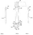
- FIG. 1shows a simplified block diagram of a plasma processing system comprising a baffle plate according to an embodiment of the present invention
- FIG. 2shows a plan view of a baffle plate for a plasma processing system according to an embodiment of the present invention
- FIG. 3shows a cross sectional view of a baffle plate for a plasma processing system according to an embodiment of the present invention
- FIG. 4shows an expanded cross sectional view taken along a minor axis of one passageway formed within a baffle plate for a plasma processing system according to an embodiment of the present invention
- FIG. 5Ashows an expanded view of one passageway formed within an upper surface of a baffle plate for a plasma processing system according to an embodiment of the present invention
- FIG. 5Bshows an expanded cross sectional view taken along a major axis of one passageway formed within a baffle plate for a plasma processing system according to an embodiment of the present invention
- FIG. 5Cshows an expanded view of one passageway formed within a lower surface of a baffle plate for a plasma processing system according to an embodiment of the present invention
- FIG. 6presents an expanded view of an inner radial edge of a baffle plate for a plasma processing system according to an embodiment of the present invention
- FIG. 7presents an expanded view of an outer radial edge of a baffle plate for a plasma processing system according to an embodiment of the present invention
- FIG. 8presents a method of producing a baffle plate for a plasma processing system according to an embodiment of the present invention
- FIG. 9presents a method of producing a baffle plate for a plasma processing system according to another embodiment of the present invention.
- FIG. 10presents a method of producing a baffle plate for a plasma processing system according to another embodiment of the present invention.
- a plasma processing system 1is depicted in FIG. 1 comprising a plasma processing chamber 10 , an upper assembly 20 , an upper electrode 22 , a substrate holder 30 for supporting a substrate 35 , and a pumping duct 40 coupled to a vacuum pump (not shown) for providing a reduced pressure atmosphere 11 in plasma processing chamber 10 .
- Plasma processing chamber 10can facilitate the formation of a processing plasma in process space 12 adjacent substrate 35 .
- the plasma processing system 1can be configured to process 200 mm substrates, 300 mm substrates, or larger.
- upper electrode 22comprises an electrode plate 24 ( FIG. 1 ) with a deposition shield 26 ( FIG. 1 ).
- upper assembly 20can comprise at least one of a cover, a gas injection assembly, and an upper electrode impedance match network.
- the upper electrode 22can be coupled to an RF source.
- the upper assembly 20comprises a cover coupled to the upper electrode 22 , wherein the upper electrode 22 is maintained at an electrical potential equivalent to that of the plasma processing chamber 10 .
- the plasma processing chamber 10 , the upper assembly 20 , and the upper electrode 22can be electrically connected to ground potential.
- Plasma processing chamber 10can, for example, further comprise an optical viewport 16 coupled to the deposition shield 26 of upper electrode 22 .
- Optical viewport 16can comprise an optical window 17 coupled to the backside of an optical window deposition shield 18 , and an optical window flange 19 can be configured to couple optical window 17 to the optical window deposition shield 18 .
- Sealing memberssuch as O-rings, can be provided between the optical window flange 19 and the optical window 17 , between the optical window 17 and the optical window deposition shield 18 , and between the optical window deposition shield 18 and the plasma processing chamber 10 .
- Optical viewport 16can, for example, permit monitoring of optical emission from the processing plasma in process space 12 .
- Substrate holder 30can, for example, further comprise a vertical translational device 50 surrounded by a bellows 52 coupled to the substrate holder 30 and the plasma processing chamber 10 , and configured to seal the vertical translational device 50 from the reduced pressure atmosphere 11 in plasma processing chamber 10 .
- a bellows shield 54can, for example, be coupled to the substrate holder 30 and configured to protect the bellows 52 from the processing plasma.
- Substrate holder 10can, for example, further be coupled to at least one of a focus ring 60 , and a shield ring 62 .
- a baffle plate 64can extend about a periphery of the substrate holder 30 .
- Substrate 35can be, for example, transferred into and out of plasma processing chamber 10 through a slot valve (not shown) and chamber feed-through (not shown) via robotic substrate transfer system where it is received by substrate lift pins (not shown) housed within substrate holder 30 and mechanically translated by devices housed therein. Once substrate 35 is received from substrate transfer system, it is lowered to an upper surface of substrate holder 30 .
- Substrate 35can be, for example, affixed to the substrate holder 30 via an electrostatic clamping system.
- substrate holder 30can, for example, further include a cooling system including a re-circulating coolant flow that receives heat from substrate holder 30 and transfers heat to a heat exchanger system (not shown), or when heating, transfers heat from the heat exchanger system.
- gascan, for example, be delivered to the backside of substrate 35 via a backside gas system to improve the gas-gap thermal conductance between substrate 35 and substrate holder 30 .
- Such a systemcan be utilized when temperature control of the substrate is required at elevated or reduced temperatures.
- heating elementssuch as resistive heating elements, or thermo-electric heaters/coolers can be included.
- substrate holder 30can comprise an electrode through which RF power is coupled to the processing plasma in process space 12 .
- substrate holder 30can be electrically biased at a RF voltage via the transmission of RF power from a RF generator (not shown) through an impedance match network (not shown) to substrate holder 30 .
- the RF biascan serve to heat electrons to form and maintain plasma.
- the systemcan operate as a reactive ion etch (RIE) reactor, wherein the chamber and upper gas injection electrode serve as ground surfaces.
- RIEreactive ion etch
- a typical frequency for the RF biascan range from 1 MHz to 100 MHz and is preferably 13.56 MHz.
- RF systems for plasma processingare well known to those skilled in the art.
- the processing plasma formed in process space 12can be formed using a parallel-plate, capacitively coupled plasma (CCP) source, an inductively coupled plasma (ICP) source, any combination thereof, and with and without magnet systems.
- the processing plasma in process space 12can be formed using electron cyclotron resonance (ECR).
- ECRelectron cyclotron resonance
- the processing plasma in process space 12is formed from the launching of a Helicon wave.
- the processing plasma in process space 12is formed from a propagating surface wave.
- baffle plate 64can form a ring comprising an upper surface 82 , a lower surface 84 , an inner radial edge 86 , and an outer radial edge 88 .
- the baffle plate 64can further comprise at least one passageway 90 coupled to the upper surface 82 and to the lower surface 84 , and configured to permit the flow of gas therethrough.
- FIG. 4provides an expanded view of one of the passageways 90 , wherein the expanded view provides a transverse cross sectional view taken along a minor axis of the passageway 90 .
- Each passageway 90comprises an inner passageway surface 92 contiguous with the upper surface 82 and the lower surface 84 of the baffle plate 64 .
- at least one passageway 90can comprise a length, dictated by the distance between the upper surface 82 and the lower surface 84 proximate each passageway 90 , having a dimensional range from 1 to 50 mm. Desirably, the length comprises a dimensional range from 1 to 10 mm, and preferably the length is at least 5 mm.
- FIGS. 5A , 5 B, and 5 Cprovide an exemplary cross-sectional view of passageway 90 at the upper surface 82 of baffle plate 64 , an additional expanded cross-sectional view of passageway 90 taken along a major axis of the passageway 90 , and an exemplary cross-sectional view of passageway 90 at the lower surface 84 of baffle plate 64 , respectively.
- the at least one passageway 90can comprise slots aligned in a radial direction.
- the slotscan be aligned in an azimuthal direction.
- the slotscan be slanted and, therefore, aligned partially in a radial direction and an azimuthal direction.
- the passageways 90can comprise a combination of alignment methodologies thereof.
- the passagewayscan include at least one orifice.
- the cross sectional view of the passageway 90 at the upper surface 82comprises a cross sectional entrance area 91 a that is greater than the respective cross sectional exit area 91 b depicted in the cross sectional view of the passageway 90 at the lower surface 84 .
- the cross sectional areacan be, for example, constant along the length of the passageway from the upper surface 82 to the lower surface 84 .
- the cross-sectional exit area 91 b of the passageway 90 at the lower surface 84can, for example, comprise a cross-sectional area greater than the respective cross-sectional entrance area 91 a of the passageway 90 at the upper surface 82 .
- baffle plate 64can, for example, further comprise a plurality of fastening receptors 100 .
- Each fastening receptor 100can be coupled to the upper surface 82 and the lower surface 84 , and configured to receive fastening devices (not shown) (such as bolts) to couple baffle plate 64 to substrate holder 30 .
- the fastening receptors 100can comprise a first entrant cavity 102 , a second entrant cavity 103 , and an exit through-hole 104 . Alternately, second entrant cavity 103 is not required.
- the number of fastening receptors 100 formed within baffle plate 64can range from 0 to 100. Desirably, the number of fastening receptors 100 ranges from 5 to 20; and, preferably, the number of fastening receptors 100 equals 12 fastening receptors.
- FIG. 6depicts an expanded cross sectional view of the inner radial edge 86 of baffle plate 64 comprising one of the plurality of fastening receptors 100 .
- the inner radial edge 86can further comprise an inner edge surface 112 and a plurality of fastener mating surfaces 113 .
- the inner edge surface 112can be coupled to the upper surface 82 and the lower surface 84 of baffle plate 64 .
- At least one of the fastener mating surfaces 113can be coupled to and coincident with the lower surface 84 of baffle plate 64 and configured to mate the baffle plate 64 with substrate holder 30 .
- FIG. 6depicts an expanded cross sectional view of the inner radial edge 86 of baffle plate 64 comprising one of the plurality of fastening receptors 100 .
- the inner radial edge 86can further comprise an inner edge surface 112 and a plurality of fastener mating surfaces 113 .
- the inner edge surface 112can be coupled to the upper surface 82 and the
- the fastening receptor 100can include an inner receptor surface 106 that can further comprise a first entrant surface 107 , a first lip surface 108 , a second entrant surface 109 , a second lip surface 110 , and an exit surface 111 .
- the inner radial edge 86can comprise a minimum thickness, dictated by a distance between the upper surface 82 and the lower surface 84 proximate the inner radial edge 86 , having a dimensional range from 1 to 50 mm. Desirably, the minimum thickness comprises a dimensional range from 1 to 10 mm, and preferably the minimum thickness is at least 2 mm.
- FIG. 7provides an expanded cross sectional view of the outer radial edge 88 of baffle plate 64 .
- the outer radial edge 88can further comprise an outer edge surface 114 , a first mating surface 116 , and a second mating surface 118 .
- the outer edge surface 114can be coupled to the upper surface 82 and the lower surface 84 of baffle plate 64 .
- the first mating surface 116can be coupled to and coincident with a portion of the upper surface 82 , and configured to mate with plasma processing system 1 .
- the second mating surface 118can be coupled to and coincident with a portion of the lower surface 84 , and configured to mate with plasma processing system 1 .
- first and second mating surfacescan be used to mate baffle plate 64 with at least one of a deposition shield 14 and a plasma processing chamber 10 .
- the outer radial edge 88can comprise a thickness, dictated by the distance between the first mating surface 116 and the second mating surface 118 proximate the outer radial edge 88 , having a dimensional range from 1 to 50 mm. Desirably, the thickness comprises a dimensional range from 1 to 10 mm, and preferably the thickness is at least 7 mm.
- baffle plate 64can, for example, further comprise a plurality of mounting through-holes 101 .
- Each mounting through-hole 101can be coupled to the upper surface 82 and the lower surface 84 , and configured to receive fastening devices (not shown) (such as bolts) to couple baffle plate 64 to at least one of the plasma processing chamber 10 and the deposition shield 26 of the upper electrode 22 .
- the number of mounting through-holes 101 formed within baffle plate 64can range from 0 to 100. Desirably, the number of mounting through-holes 101 ranges from 5 to 20; and, preferably, the number of mounting through-holes 101 is at least 10.
- the baffle plate 64further comprises a protective barrier 150 formed on a plurality of exposed surfaces 145 of the baffle plate 64 .
- the exposed surfaces 145can comprise the upper surface 82 of baffle plate 64 excluding the first mating surface 116 ; the lower surface 84 of baffle plate 64 excluding the plurality of fastener mating surfaces 113 and the second mating surface 118 ; and the inner passageway surface 92 contiguous with the upper surface 82 and the lower surface 84 .
- the exposed surfaces 145can comprise the first entrant surface 107 of each of the plurality of fastening receptors 100 ; and the first lip surface 108 of each of the plurality of fastening receptors 100 .
- the exposed surfacescomprise all surfaces on the baffle plate 64 .
- the protective barrier 150can comprise a compound including an oxide of aluminum such as Al 2 O 3 . In another embodiment of the present invention, the protective barrier 150 can comprise a mixture of Al 2 O 3 and Y 2 O 3 . In another embodiment of the present invention, the protective barrier 150 can comprise at least one of a III-column element (column III of periodic table) and a Lanthanon element. In another embodiment of the present invention, the III-column element can comprise at least one of Yttrium, Scandium, and Lanthanum. In another embodiment of the present invention, the Lanthanon element can comprise at least one of Cerium, Dysprosium, and Europium.
- the compound forming protective barrier 150can comprise at least one of Yttria (Y 2 O 3 ), Sc 2 O 3 , Sc 2 F 3 , YF 3 , La 2 O 3 , CeO 2 , Eu 2 O 3 and DyO 3 .
- the protective barrier 150 formed on baffle plate 64comprises a thermal sprayed coating having a minimum thickness, wherein the minimum thickness can be allowed to vary across the plurality of exposed surfaces 145 .
- the specified thicknesscan be variable across the exposed surfaces 145 .
- the minimum thicknesscan be constant over a first portion of the exposed surfaces 145 and variable over a second portion of the exposed surfaces 145 .
- a variable thicknesscan occur on a curved surface, on a corner, or in a hole.
- the minimum thicknessranges from 0 micron to 550 micron. Desirably, the minimum thickness ranges from 50 micron to 250 micron; and, preferably, the minimum thickness ranges from 150 micron to 250 micron.
- FIG. 8presents a method of producing the baffle plate 64 in the plasma processing system described in FIG. 1 according to an embodiment of the present invention.
- a flow diagram 300begins in 310 with fabricating the baffle plate 64 (e.g., a baffle plate having the characteristics of the plate described with reference to FIGS. 2-7 ).
- Fabricating the baffle platecan comprise at least one of machining, casting, polishing, forging, and grinding.
- each of the elements described abovecan be machined according to specifications set forth on a mechanical drawing, using conventional techniques including a mill, a lathe, etc.
- the techniques for machining a component using, for example, a mill or a latheare well known to those skilled in the art of machining.
- the baffle platecan, for example, be fabricated from aluminum.
- the baffle plateis anodized to form a surface anodization layer.
- the surface anodization layercomprises aluminum oxide (Al 2 O 3 ). Methods of anodizing aluminum components are well known to those skilled in the art of surface anodization.
- the surface anodization layeris removed from the exposed surfaces 145 using standard machining techniques.
- other surfacese.g., the first mating surface of the upper surface, the second mating surface of the lower surface, and the plurality of fastener mating surfaces of the lower surface
- may also be machinede.g., to produce a flat or bare surface that provides at least one of a good mechanical or electrical contact at the machined surface.
- the protective barrier 150is formed on the exposed surfaces 145 .
- a protective barrier 150comprising, for example Yttria, can be formed using (thermal) spray coating techniques that are well known to those skilled in the art of ceramic spray coatings.
- forming the protective barriercan further comprise polishing the thermal spray coating.
- polishing the thermal spray coatingcan comprise the application of sand paper to the sprayed surfaces.
- FIG. 9presents a method of producing the baffle plate in the plasma processing system described in FIG. 1 according to another embodiment of the present invention.
- a flow diagram 400begins in 410 with fabricating the baffle plate 64 (e.g., a baffle plate having the characteristics of the plate described with reference to FIGS. 2-7 ).
- Fabricating the baffle platecan comprise at least one of machining, casting, polishing, forging, and grinding.
- each of the elements described abovecan be machined according to specifications set forth on a mechanical drawing, using conventional techniques including a mill, a lathe, etc.
- the techniques for machining a component using, for example, a mill or a latheare well known to those skilled in the art of machining.
- the baffle platecan, for example, be fabricated from aluminum.
- exposed surfaces 145are masked to prevent the formation of a surface anodization layer thereon.
- Techniques for surface masking and unmaskingare well known to those skilled in the art of surface coatings and surface anodization.
- other surfacese.g., the first mating surface of the upper surface, the second mating surface of the lower surface, and the plurality of fastener mating surfaces of the lower surface
- may also be maskede.g., to maintain a flat or bare surface that provides at least one of a good mechanical or electrical contact at the machined surface).
- the baffle plateis anodized to form a surface anodization layer on the remaining unmasked surfaces.
- the surface anodization layercan comprise aluminum oxide (Al 2 O 3 ). Methods of anodizing aluminum components are well known to those skilled in the art of surface anodization.
- the protective barrier 150is formed on the exposed surfaces.
- a protective barriercomprising, for example Yttria, can be formed using (thermal) spray coating techniques that are well known to those skilled in the art of ceramic spray coatings.
- forming the protective barriercan further comprise polishing the thermal spray coating.
- polishing the thermal spray coatingcan comprise the application of sand paper to the sprayed surfaces.
- FIG. 10presents a method of producing the baffle plate in the plasma processing system described in FIG. 1 according to another embodiment of the present invention.
- a flow diagram 500begins in 510 with fabricating the baffle plate 64 (e.g., a baffle plate having the characteristics of the plate described with reference to FIGS. 2-7 ).
- Fabricating the baffle platecan comprise at least one of machining, casting, polishing, forging, and grinding.
- each of the elements described abovecan be machined according to specifications set forth on a mechanical drawing, using conventional techniques including a mill, a lathe, etc.
- the techniques for machining a component using, for example, a mill or a latheare well known to those skilled in the art of machining.
- the baffle platecan, for example, be fabricated from aluminum.
- a protective barrier 150is formed on exposed surfaces 145 of the baffle plate 64 .
- a protective barriercomprising, for example Yttria, can be formed using (thermal) spray coating techniques that are well known to those skilled in the art of ceramic spray coatings.
- forming the protective barriercan further comprise polishing the thermal spray coating.
- polishing the thermal spray coatingcan comprise the application of sand paper to the sprayed surfaces.
- the processes of forming a protective barrier 150 on the exposed surfaces 145can be modified to utilize a combination of machining and masking.
- at least one exposed surfaceis masked to prevent formation of the anodization layer thereon while other exposed surfaces are anodized.
- the exposed surfaces that are unmaskedare then machined, and the exposed surfaces that were masked are unmasked.
- the protective barrier 150can then be formed on all the exposed surfaces.
- additional surfaces that are not exposed surfacesmay also be machined during the method (e.g., in order to provide a better mechanical or electrical contact than would be formed with the anodization layer thereon.
Landscapes
- Engineering & Computer Science (AREA)
- Physics & Mathematics (AREA)
- Plasma & Fusion (AREA)
- Chemical & Material Sciences (AREA)
- Analytical Chemistry (AREA)
- General Physics & Mathematics (AREA)
- Condensed Matter Physics & Semiconductors (AREA)
- Manufacturing & Machinery (AREA)
- Computer Hardware Design (AREA)
- Microelectronics & Electronic Packaging (AREA)
- Power Engineering (AREA)
- Drying Of Semiconductors (AREA)
- Plasma Technology (AREA)
- Treatment Of Fiber Materials (AREA)
- Chemical Vapour Deposition (AREA)
Abstract
Description
Claims (26)
Priority Applications (1)
| Application Number | Priority Date | Filing Date | Title |
|---|---|---|---|
| US11/745,185US8057600B2 (en) | 2002-09-30 | 2007-05-07 | Method and apparatus for an improved baffle plate in a plasma processing system |
Applications Claiming Priority (3)
| Application Number | Priority Date | Filing Date | Title |
|---|---|---|---|
| US10/259,382US6837966B2 (en) | 2002-09-30 | 2002-09-30 | Method and apparatus for an improved baffle plate in a plasma processing system |
| US11/010,373US7282112B2 (en) | 2002-09-30 | 2004-12-14 | Method and apparatus for an improved baffle plate in a plasma processing system |
| US11/745,185US8057600B2 (en) | 2002-09-30 | 2007-05-07 | Method and apparatus for an improved baffle plate in a plasma processing system |
Related Parent Applications (1)
| Application Number | Title | Priority Date | Filing Date |
|---|---|---|---|
| US11/010,373ContinuationUS7282112B2 (en) | 2002-09-30 | 2004-12-14 | Method and apparatus for an improved baffle plate in a plasma processing system |
Publications (2)
| Publication Number | Publication Date |
|---|---|
| US20070204794A1 US20070204794A1 (en) | 2007-09-06 |
| US8057600B2true US8057600B2 (en) | 2011-11-15 |
Family
ID=32029497
Family Applications (3)
| Application Number | Title | Priority Date | Filing Date |
|---|---|---|---|
| US10/259,382Expired - LifetimeUS6837966B2 (en) | 2002-09-30 | 2002-09-30 | Method and apparatus for an improved baffle plate in a plasma processing system |
| US11/010,373Expired - LifetimeUS7282112B2 (en) | 2002-09-30 | 2004-12-14 | Method and apparatus for an improved baffle plate in a plasma processing system |
| US11/745,185Expired - Fee RelatedUS8057600B2 (en) | 2002-09-30 | 2007-05-07 | Method and apparatus for an improved baffle plate in a plasma processing system |
Family Applications Before (2)
| Application Number | Title | Priority Date | Filing Date |
|---|---|---|---|
| US10/259,382Expired - LifetimeUS6837966B2 (en) | 2002-09-30 | 2002-09-30 | Method and apparatus for an improved baffle plate in a plasma processing system |
| US11/010,373Expired - LifetimeUS7282112B2 (en) | 2002-09-30 | 2004-12-14 | Method and apparatus for an improved baffle plate in a plasma processing system |
Country Status (6)
| Country | Link |
|---|---|
| US (3) | US6837966B2 (en) |
| JP (1) | JP4627660B2 (en) |
| KR (1) | KR100733167B1 (en) |
| CN (1) | CN100380564C (en) |
| AU (1) | AU2003274581A1 (en) |
| WO (1) | WO2004030013A2 (en) |
Cited By (7)
| Publication number | Priority date | Publication date | Assignee | Title |
|---|---|---|---|---|
| US20090314432A1 (en)* | 2008-06-23 | 2009-12-24 | Tokyo Electron Limited | Baffle plate and substrate processing apparatus |
| US20110031214A1 (en)* | 2009-08-06 | 2011-02-10 | Jisoo Kim | Vacuum processing chambers incorporating a moveable flow equalizer |
| US20140361690A1 (en)* | 2011-12-27 | 2014-12-11 | Tokyo Electron Limited | Plasma processing apparatus |
| US10276340B1 (en) | 2017-12-20 | 2019-04-30 | Varian Semiconductor Equipment Associates, Inc. | Low particle capacitively coupled components for workpiece processing |
| US11053587B2 (en)* | 2012-12-21 | 2021-07-06 | Novellus Systems, Inc. | Radical source design for remote plasma atomic layer deposition |
| US11608559B2 (en) | 2016-12-14 | 2023-03-21 | Lam Research Corporation | Integrated showerhead with thermal control for delivering radical and precursor gas to a downstream chamber to enable remote plasma film deposition |
| US12116669B2 (en) | 2017-12-08 | 2024-10-15 | Lam Research Corporation | Integrated showerhead with improved hole pattern for delivering radical and precursor gas to a downstream chamber to enable remote plasma film deposition |
Families Citing this family (57)
| Publication number | Priority date | Publication date | Assignee | Title |
|---|---|---|---|---|
| KR20010062209A (en)* | 1999-12-10 | 2001-07-07 | 히가시 데쓰로 | Processing apparatus with a chamber having therein a high-etching resistant sprayed film |
| JP3510993B2 (en)* | 1999-12-10 | 2004-03-29 | トーカロ株式会社 | Plasma processing container inner member and method for manufacturing the same |
| JP4592856B2 (en)* | 1999-12-24 | 2010-12-08 | 東京エレクトロン株式会社 | Baffle plate and gas treatment device |
| JP4602532B2 (en)* | 2000-11-10 | 2010-12-22 | 東京エレクトロン株式会社 | Plasma processing equipment |
| JP2002198355A (en)* | 2000-12-26 | 2002-07-12 | Tokyo Electron Ltd | Plasma treatment apparatus |
| AU2002227418A1 (en)* | 2001-01-22 | 2002-08-06 | Tokyo Electron Limited | Vertically translatable chuck assembly and method for a plasma reactor system |
| US20040129218A1 (en)* | 2001-12-07 | 2004-07-08 | Toshiki Takahashi | Exhaust ring mechanism and plasma processing apparatus using the same |
| US7147749B2 (en)* | 2002-09-30 | 2006-12-12 | Tokyo Electron Limited | Method and apparatus for an improved upper electrode plate with deposition shield in a plasma processing system |
| US7166200B2 (en)* | 2002-09-30 | 2007-01-23 | Tokyo Electron Limited | Method and apparatus for an improved upper electrode plate in a plasma processing system |
| US7166166B2 (en) | 2002-09-30 | 2007-01-23 | Tokyo Electron Limited | Method and apparatus for an improved baffle plate in a plasma processing system |
| US6798519B2 (en)* | 2002-09-30 | 2004-09-28 | Tokyo Electron Limited | Method and apparatus for an improved optical window deposition shield in a plasma processing system |
| US6837966B2 (en)* | 2002-09-30 | 2005-01-04 | Tokyo Electron Limeted | Method and apparatus for an improved baffle plate in a plasma processing system |
| US7137353B2 (en)* | 2002-09-30 | 2006-11-21 | Tokyo Electron Limited | Method and apparatus for an improved deposition shield in a plasma processing system |
| US7204912B2 (en)* | 2002-09-30 | 2007-04-17 | Tokyo Electron Limited | Method and apparatus for an improved bellows shield in a plasma processing system |
| US7780786B2 (en)* | 2002-11-28 | 2010-08-24 | Tokyo Electron Limited | Internal member of a plasma processing vessel |
| US6844260B2 (en)* | 2003-01-30 | 2005-01-18 | Micron Technology, Inc. | Insitu post atomic layer deposition destruction of active species |
| JP4597972B2 (en) | 2003-03-31 | 2010-12-15 | 東京エレクトロン株式会社 | A method of bonding adjacent coatings on a processing member. |
| KR101016913B1 (en)* | 2003-03-31 | 2011-02-22 | 도쿄엘렉트론가부시키가이샤 | Barrier layer for processing element and method of forming the same |
| US20050011447A1 (en)* | 2003-07-14 | 2005-01-20 | Tokyo Electron Limited | Method and apparatus for delivering process gas to a process chamber |
| US7001482B2 (en)* | 2003-11-12 | 2006-02-21 | Tokyo Electron Limited | Method and apparatus for improved focus ring |
| US7461614B2 (en)* | 2003-11-12 | 2008-12-09 | Tokyo Electron Limited | Method and apparatus for improved baffle plate |
| US8349128B2 (en)* | 2004-06-30 | 2013-01-08 | Applied Materials, Inc. | Method and apparatus for stable plasma processing |
| US20060000802A1 (en)* | 2004-06-30 | 2006-01-05 | Ajay Kumar | Method and apparatus for photomask plasma etching |
| US20060037702A1 (en)* | 2004-08-20 | 2006-02-23 | Tokyo Electron Limited | Plasma processing apparatus |
| US7552521B2 (en)* | 2004-12-08 | 2009-06-30 | Tokyo Electron Limited | Method and apparatus for improved baffle plate |
| US7601242B2 (en)* | 2005-01-11 | 2009-10-13 | Tokyo Electron Limited | Plasma processing system and baffle assembly for use in plasma processing system |
| JP4409459B2 (en)* | 2005-02-17 | 2010-02-03 | 東京エレクトロン株式会社 | Plasma processing apparatus and its component and component life detection method |
| US7198677B2 (en)* | 2005-03-09 | 2007-04-03 | Wafermasters, Inc. | Low temperature wafer backside cleaning |
| US20060225654A1 (en)* | 2005-03-29 | 2006-10-12 | Fink Steven T | Disposable plasma reactor materials and methods |
| US7313310B2 (en)* | 2005-05-25 | 2007-12-25 | Honeywell International Inc. | Plasma directing baffle and method of use |
| US7462845B2 (en)* | 2005-12-09 | 2008-12-09 | International Business Machines Corporation | Removable liners for charged particle beam systems |
| US7416677B2 (en) | 2006-08-11 | 2008-08-26 | Tokyo Electron Limited | Exhaust assembly for plasma processing system and method |
| US7909961B2 (en)* | 2006-10-30 | 2011-03-22 | Applied Materials, Inc. | Method and apparatus for photomask plasma etching |
| US7943005B2 (en) | 2006-10-30 | 2011-05-17 | Applied Materials, Inc. | Method and apparatus for photomask plasma etching |
| US8034410B2 (en) | 2007-07-17 | 2011-10-11 | Asm International N.V. | Protective inserts to line holes in parts for semiconductor process equipment |
| CN101355009B (en)* | 2007-07-23 | 2011-11-02 | 北京北方微电子基地设备工艺研究中心有限责任公司 | Etching device |
| US7807222B2 (en)* | 2007-09-17 | 2010-10-05 | Asm International N.V. | Semiconductor processing parts having apertures with deposited coatings and methods for forming the same |
| TWI471961B (en)* | 2007-10-26 | 2015-02-01 | Sosul Co Ltd | Baffle, substrate supporting apparatus and plasma processing apparatus and plasma processing method |
| US20090178763A1 (en)* | 2008-01-10 | 2009-07-16 | Applied Materials, Inc. | Showerhead insulator and etch chamber liner |
| JP2009200184A (en)* | 2008-02-20 | 2009-09-03 | Tokyo Electron Ltd | Plasma processing apparatus, and baffle plate of plasma processing apparatus |
| US7987814B2 (en)* | 2008-04-07 | 2011-08-02 | Applied Materials, Inc. | Lower liner with integrated flow equalizer and improved conductance |
| JP5424744B2 (en)* | 2009-07-01 | 2014-02-26 | 株式会社フェローテック | Divided annular rib plasma processing equipment |
| JP5302813B2 (en)* | 2009-07-28 | 2013-10-02 | 東京エレクトロン株式会社 | Deposit control cover and plasma processing apparatus |
| JP5443096B2 (en)* | 2009-08-12 | 2014-03-19 | 株式会社ニューフレアテクノロジー | Semiconductor manufacturing apparatus and semiconductor manufacturing method |
| US20110220285A1 (en)* | 2010-02-12 | 2011-09-15 | Morgan Advanced Ceramics, Inc. | Methods and systems for texturing ceramic components |
| KR20120065841A (en)* | 2010-12-13 | 2012-06-21 | 삼성전자주식회사 | Substrate support unit, and apparatus for depositing thin layer using the same |
| US20140051253A1 (en)* | 2012-08-14 | 2014-02-20 | Lam Research Corporation | Plasma baffle ring for a plasma processing apparatus and method of use |
| US10777387B2 (en)* | 2012-09-28 | 2020-09-15 | Semes Co., Ltd. | Apparatus for treating substrate |
| JP6544902B2 (en)* | 2014-09-18 | 2019-07-17 | 東京エレクトロン株式会社 | Plasma processing system |
| US12281385B2 (en)* | 2015-06-15 | 2025-04-22 | Taiwan Semiconductor Manufacturing Co., Ltd. | Gas dispenser and deposition apparatus using the same |
| JP6994502B2 (en)* | 2016-08-26 | 2022-01-14 | アプライド マテリアルズ インコーポレイテッド | Plasma screen for plasma processing chamber |
| CN111383884B (en)* | 2018-12-27 | 2023-03-10 | 中微半导体设备(上海)股份有限公司 | Plasma confinement system and method |
| US12359313B2 (en)* | 2019-07-31 | 2025-07-15 | Taiwan Semiconductor Manufacturing Company, Ltd. | Deposition apparatus and method of forming metal oxide layer using the same |
| US12100577B2 (en)* | 2019-08-28 | 2024-09-24 | Applied Materials, Inc. | High conductance inner shield for process chamber |
| US20210066051A1 (en)* | 2019-08-28 | 2021-03-04 | Applied Materials, Inc. | High conductance lower shield for process chamber |
| CN113745083B (en)* | 2020-05-28 | 2023-09-29 | 中微半导体设备(上海)股份有限公司 | Plasma processing device |
| JP7586598B2 (en)* | 2021-01-08 | 2024-11-19 | 東京エレクトロン株式会社 | Exhaust ring assembly and plasma processing apparatus |
Citations (177)
| Publication number | Priority date | Publication date | Assignee | Title |
|---|---|---|---|---|
| US4310390A (en) | 1977-08-10 | 1982-01-12 | Lockheed Corporation | Protective coating process for aluminum and aluminum alloys |
| US4357387A (en) | 1981-08-20 | 1982-11-02 | Subtex, Inc. | Flame resistant insulating fabric compositions prepared by plasma spraying |
| US4469619A (en) | 1981-09-30 | 1984-09-04 | Sony Corporation | Method of manufacturing a green phosphor |
| US4593007A (en) | 1984-12-06 | 1986-06-03 | The Perkin-Elmer Corporation | Aluminum and silica clad refractory oxide thermal spray powder |
| US4612077A (en) | 1985-07-29 | 1986-09-16 | The Perkin-Elmer Corporation | Electrode for plasma etching system |
| US4649858A (en) | 1984-10-12 | 1987-03-17 | Sumitomo Metal Industries, Ltd. | Repairing apparatus for furnace wall |
| US4842683A (en)* | 1986-12-19 | 1989-06-27 | Applied Materials, Inc. | Magnetic field-enhanced plasma etch reactor |
| EP0326318A2 (en) | 1988-01-25 | 1989-08-02 | Elkem Technology A/S | Plasma torch |
| US4877757A (en) | 1987-07-16 | 1989-10-31 | Texas Instruments Incorporated | Method of sequential cleaning and passivating a GaAs substrate using remote oxygen plasma |
| US5000113A (en) | 1986-12-19 | 1991-03-19 | Applied Materials, Inc. | Thermal CVD/PECVD reactor and use for thermal chemical vapor deposition of silicon dioxide and in-situ multi-step planarized process |
| US5074456A (en) | 1990-09-18 | 1991-12-24 | Lam Research Corporation | Composite electrode for plasma processes |
| US5126102A (en) | 1990-03-15 | 1992-06-30 | Kabushiki Kaisha Toshiba | Fabricating method of composite material |
| US5180467A (en) | 1990-08-08 | 1993-01-19 | Vlsi Technology, Inc. | Etching system having simplified diffuser element removal |
| EP0573057A1 (en) | 1992-06-05 | 1993-12-08 | Applied Materials, Inc. | Integrated circuit structure processing apparatus with chemically corrosion-resistant Al2O3 protective coating on surface of quartz window exposed to corrosive chemicals |
| US5302465A (en) | 1992-10-26 | 1994-04-12 | The United States Of America As Represented By The Administrator Of The National Aeronautics And Space Administration | Plasma sprayed ceramic thermal barrier coating for NiAl-based intermetallic alloys |
| US5334462A (en) | 1989-09-08 | 1994-08-02 | United Technologies Corporation | Ceramic material and insulating coating made thereof |
| GB2252567B (en) | 1991-02-11 | 1994-09-14 | Inst Elektroswarki Patona | Metal/ceramic protective coating for superalloy articles |
| US5362335A (en) | 1993-03-25 | 1994-11-08 | General Motors Corporation | Rare earth coating process for aluminum alloys |
| US5366585A (en) | 1993-01-28 | 1994-11-22 | Applied Materials, Inc. | Method and apparatus for protection of conductive surfaces in a plasma processing reactor |
| US5367838A (en) | 1992-06-01 | 1994-11-29 | Ice Blast International, Inc. | Particle blasting using crystalline ice |
| US5423936A (en) | 1992-10-19 | 1995-06-13 | Hitachi, Ltd. | Plasma etching system |
| US5426310A (en) | 1989-07-11 | 1995-06-20 | Sony Corporation | Method of heat-treating an oxide optical crystal and a heat treatment apparatus for carrying out the same |
| US5484752A (en) | 1993-11-12 | 1996-01-16 | Ube Industries, Ltd. | Ceramic composite material |
| US5489449A (en) | 1990-03-28 | 1996-02-06 | Nisshin Flour Milling Co., Ltd. | Coated particles of inorganic or metallic materials and processes of producing the same |
| US5494713A (en) | 1994-02-03 | 1996-02-27 | Tokyo Electron Limited | Method for treating surface of aluminum material and plasma treating apparatus |
| US5521790A (en) | 1994-05-12 | 1996-05-28 | International Business Machines Corporation | Electrostatic chuck having relatively thick and thin areas and means for uniformly cooling said thick and thin areas during chuck anodization |
| US5534356A (en) | 1995-04-26 | 1996-07-09 | Olin Corporation | Anodized aluminum substrate having increased breakdown voltage |
| DE9421671U1 (en) | 1994-08-26 | 1996-07-11 | Siemens AG, 80333 München | Discharge chamber for a plasma etching system in semiconductor production |
| US5551190A (en) | 1993-05-19 | 1996-09-03 | Ohi Seisakusho Co., Ltd. | Slide door driving system |
| US5556501A (en) | 1989-10-03 | 1996-09-17 | Applied Materials, Inc. | Silicon scavenger in an inductively coupled RF plasma reactor |
| EP0508731B1 (en) | 1991-04-09 | 1996-09-18 | The Tokyo Electric Power Co., Inc. | Use of an oxide coating to enhance the resistance to oxidation and corrosion of a silicon nitride based gas turbine blade |
| US5614055A (en) | 1993-08-27 | 1997-03-25 | Applied Materials, Inc. | High density plasma CVD and etching reactor |
| US5637237A (en) | 1994-03-08 | 1997-06-10 | International Business Machines Corporation | Method for hot wall reactive ion etching using a dielectric or metallic liner with temperature control to achieve process stability |
| US5641375A (en)* | 1994-08-15 | 1997-06-24 | Applied Materials, Inc. | Plasma etching reactor with surface protection means against erosion of walls |
| US5651723A (en) | 1994-04-13 | 1997-07-29 | Viratec Thin Films, Inc. | Method and apparatus for cleaning substrates in preparation for deposition of thin film coatings |
| US5680013A (en) | 1994-03-15 | 1997-10-21 | Applied Materials, Inc. | Ceramic protection for heated metal surfaces of plasma processing chamber exposed to chemically aggressive gaseous environment therein and method of protecting such heated metal surfaces |
| US5716534A (en)* | 1994-12-05 | 1998-02-10 | Tokyo Electron Limited | Plasma processing method and plasma etching method |
| US5725960A (en) | 1992-12-28 | 1998-03-10 | Nippon Zeon Co., Ltd. | Molded articles having hard coat layer and method for producing same |
| US5759360A (en) | 1995-03-13 | 1998-06-02 | Applied Materials, Inc. | Wafer clean sputtering process |
| EP0814495A3 (en) | 1996-06-20 | 1998-08-12 | Applied Materials, Inc. | Adjusting DC bias voltage in plasma chamber |
| US5820723A (en) | 1996-06-05 | 1998-10-13 | Lam Research Corporation | Universal vacuum chamber including equipment modules such as a plasma generating source, vacuum pumping arrangement and/or cantilevered substrate support |
| US5834070A (en) | 1996-04-04 | 1998-11-10 | International Center For Electron Beam Technologies Of E.O. Paton Electric Welding Institute | Method of producing protective coatings with chemical composition and structure gradient across the thickness |
| US5851343A (en) | 1997-05-16 | 1998-12-22 | Taiwan Semiconductor Manufacturing Company, Ltd. | Protective shield around the inner edge of endpoint window in a plasma etching chamber |
| US5868848A (en) | 1995-06-07 | 1999-02-09 | Tokyo Electron Limited | Plasma processing apparatus |
| KR19990008937U (en) | 1997-08-13 | 1999-03-05 | 이문세 | Soundproof wall assembly |
| US5879575A (en) | 1995-11-29 | 1999-03-09 | Applied Materials, Inc. | Self-cleaning plasma processing reactor |
| US5882411A (en) | 1996-10-21 | 1999-03-16 | Applied Materials, Inc. | Faceplate thermal choke in a CVD plasma reactor |
| US5885356A (en) | 1994-11-30 | 1999-03-23 | Applied Materials, Inc. | Method of reducing residue accumulation in CVD chamber using ceramic lining |
| US5885402A (en) | 1996-07-17 | 1999-03-23 | Applied Materials | Diagnostic head assembly for plasma chamber |
| US5891253A (en) | 1993-05-14 | 1999-04-06 | Applied Materials, Inc. | Corrosion resistant apparatus |
| US5892278A (en) | 1996-05-24 | 1999-04-06 | Dai Nippon Printingco., Ltd. | Aluminum and aluminum alloy radiator for semiconductor device and process for producing the same |
| US5894887A (en) | 1995-11-30 | 1999-04-20 | Applied Materials, Inc. | Ceramic dome temperature control using heat pipe structure and method |
| US5895586A (en) | 1994-05-17 | 1999-04-20 | Hitachi, Ltd. | Plasma processing apparatus and plasma processing method in which a part of the processing chamber is formed using a pre-fluorinated material of aluminum |
| US5900064A (en) | 1997-05-01 | 1999-05-04 | Applied Materials, Inc. | Plasma process chamber |
| US5902763A (en) | 1995-01-19 | 1999-05-11 | Ube Industries, Inc. | Fused ceramic composite |
| US5904778A (en) | 1996-07-26 | 1999-05-18 | Applied Materials, Inc. | Silicon carbide composite article particularly useful for plasma reactors |
| US5911852A (en) | 1995-06-15 | 1999-06-15 | Sumitomo Metal Industries Limited | Plasma processing apparatus |
| US5919332A (en) | 1995-06-07 | 1999-07-06 | Tokyo Electron Limited | Plasma processing apparatus |
| US5925228A (en) | 1997-01-09 | 1999-07-20 | Sandia Corporation | Electrophoretically active sol-gel processes to backfill, seal, and/or densify porous, flawed, and/or cracked coatings on electrically conductive material |
| US5944902A (en) | 1997-02-10 | 1999-08-31 | Applied Materials, Inc. | Plasma source for HDP-CVD chamber |
| US5948521A (en) | 1995-08-11 | 1999-09-07 | Siemens Aktiengesellscahft | Thermally conductive, electrically insulating connection |
| US5952060A (en) | 1996-06-14 | 1999-09-14 | Applied Materials, Inc. | Use of carbon-based films in extending the lifetime of substrate processing system components |
| US5952054A (en) | 1996-02-28 | 1999-09-14 | Nippon Steel Hardfacing Co., Ltd. | Method of forming spray deposit and integrated sealer layer |
| US5955182A (en) | 1996-02-05 | 1999-09-21 | Kabushiki Kaisha Toshiba | Heat resisting member and its production method |
| US5968377A (en) | 1996-05-24 | 1999-10-19 | Sekisui Chemical Co., Ltd. | Treatment method in glow-discharge plasma and apparatus thereof |
| US5985102A (en) | 1996-01-29 | 1999-11-16 | Micron Technology, Inc. | Kit for electrically isolating collimator of PVD chamber, chamber so modified, and method of using |
| US5994662A (en) | 1997-05-29 | 1999-11-30 | Applied Materials, Inc. | Unique baffle to deflect remote plasma clean gases |
| JP2000119840A (en) | 1998-10-09 | 2000-04-25 | Kyodo International:Kk | Cleaning method of film-forming device, cleaning method of sputtering target and cleaning device used therefor |
| JP2000124197A (en) | 1998-10-16 | 2000-04-28 | Hitachi Ltd | Plasma processing equipment |
| US6068729A (en) | 1997-03-03 | 2000-05-30 | Applied Materials, Inc. | Two step process for cleaning a substrate processing chamber |
| US6073449A (en) | 1996-06-25 | 2000-06-13 | Technova Inc. | Thermoelectric apparatus |
| US6079356A (en) | 1997-12-02 | 2000-06-27 | Applied Materials, Inc. | Reactor optimized for chemical vapor deposition of titanium |
| US6082444A (en) | 1997-02-21 | 2000-07-04 | Tocalo Co., Ltd. | Heating tube for boilers and method of manufacturing the same |
| US6096161A (en) | 1997-12-24 | 2000-08-01 | Samsung Electronics Co., Ltd. | Dry etching apparatus having means for preventing micro-arcing |
| US6106625A (en) | 1997-12-02 | 2000-08-22 | Applied Materials, Inc. | Reactor useful for chemical vapor deposition of titanium nitride |
| US6108189A (en) | 1996-04-26 | 2000-08-22 | Applied Materials, Inc. | Electrostatic chuck having improved gas conduits |
| US6110287A (en) | 1993-03-31 | 2000-08-29 | Tokyo Electron Limited | Plasma processing method and plasma processing apparatus |
| US6120955A (en) | 1997-06-27 | 2000-09-19 | Minolta Co., Ltd. | Substrate for photosensitive member, photosensitive member, production method thereof and image forming apparatus using the photosensitive member |
| US6120640A (en) | 1996-12-19 | 2000-09-19 | Applied Materials, Inc. | Boron carbide parts and coatings in a plasma reactor |
| US6123804A (en) | 1999-02-22 | 2000-09-26 | Applied Materials, Inc. | Sectional clamp ring |
| US6123791A (en) | 1998-07-29 | 2000-09-26 | Applied Materials, Inc. | Ceramic composition for an apparatus and method for processing a substrate |
| US6129808A (en) | 1998-03-31 | 2000-10-10 | Lam Research Corporation | Low contamination high density plasma etch chambers and methods for making the same |
| US6139983A (en) | 1997-07-15 | 2000-10-31 | Ngk Insulators, Ltd. | Corrosion-resistant member, wafer-supporting member, and method of manufacturing the same |
| JP2000303180A (en) | 1999-04-16 | 2000-10-31 | Hitachi Ltd | Processing equipment |
| KR100266840B1 (en) | 1991-05-13 | 2000-11-01 | 이데이 노부유끼 | CVD equipment |
| US6143646A (en) | 1997-06-03 | 2000-11-07 | Motorola Inc. | Dual in-laid integrated circuit structure with selectively positioned low-K dielectric isolation and method of formation |
| US6156151A (en)* | 1996-07-19 | 2000-12-05 | Tokyo Electron Limited | Plasma processing apparatus |
| US6170429B1 (en) | 1998-09-30 | 2001-01-09 | Lam Research Corporation | Chamber liner for semiconductor process chambers |
| KR100275831B1 (en) | 1995-05-30 | 2001-01-15 | 니시히라 쥰지 | Removal method of the inner surface of the vacuum container in the vacuum processing system and its vacuum processing system |
| US6176969B1 (en)* | 1998-04-22 | 2001-01-23 | Samsung Electronics Co., Ltd. | Baffle plate of dry etching apparatus for manufacturing semiconductor devices |
| US6178919B1 (en) | 1998-12-28 | 2001-01-30 | Lam Research Corporation | Perforated plasma confinement ring in plasma reactors |
| US6182603B1 (en) | 1998-07-13 | 2001-02-06 | Applied Komatsu Technology, Inc. | Surface-treated shower head for use in a substrate processing chamber |
| JP2001031484A (en) | 1999-07-22 | 2001-02-06 | Nihon Ceratec Co Ltd | Corrosion-resistant composite member |
| US6210486B1 (en) | 1997-07-16 | 2001-04-03 | Tokyo Electron Limited | CVD film forming method in which a film formation preventing gas is supplied in a direction from a rear surface of an object to be processed |
| US6221202B1 (en) | 1999-04-01 | 2001-04-24 | International Business Machines Corporation | Efficient plasma containment structure |
| JP2001152307A (en) | 1999-11-29 | 2001-06-05 | Nippon Steel Hardfacing Co Ltd | Method of forming corrosion resisting combined coating standing long use, and member having the composite coating |
| US6246479B1 (en) | 1998-06-08 | 2001-06-12 | Lj Laboratories, L.L.C. | Integrated spectrometer assembly and methods |
| US20010003271A1 (en) | 1999-12-10 | 2001-06-14 | Tokyo Electron Limited | Processing apparatus with a chamber having therein a high-corrosion-resistant sprayed film |
| JP2001164354A (en) | 1999-12-10 | 2001-06-19 | Tocalo Co Ltd | Member inside plasma treatment chamber, and manufacturing method therefor |
| US6266133B1 (en) | 1998-05-06 | 2001-07-24 | Canon Kabushiki Kaisha | Stage device, an exposure apparatus and a device manufacturing method using the same |
| US6265757B1 (en) | 1999-11-09 | 2001-07-24 | Agere Systems Guardian Corp. | Forming attached features on a semiconductor substrate |
| US6264788B1 (en) | 1994-04-20 | 2001-07-24 | Tokyo Electron Limited | Plasma treatment method and apparatus |
| US6296716B1 (en) | 1999-10-01 | 2001-10-02 | Saint-Gobain Ceramics And Plastics, Inc. | Process for cleaning ceramic articles |
| US6296740B1 (en) | 1995-04-24 | 2001-10-02 | Si Diamond Technology, Inc. | Pretreatment process for a surface texturing process |
| US20010050144A1 (en) | 1999-07-05 | 2001-12-13 | Kazuyasu Nishikawa | Plasma processing apparatus |
| US6335293B1 (en) | 1998-07-13 | 2002-01-01 | Mattson Technology, Inc. | Systems and methods for two-sided etch of a semiconductor substrate |
| US20020018921A1 (en) | 2000-04-18 | 2002-02-14 | Ngk Insulators, Ltd. | Halogen gas plasma-resistive members and method for producing the same, laminates, and corrosion-resistant members |
| US6364949B1 (en) | 1999-10-19 | 2002-04-02 | Applied Materials, Inc. | 300 mm CVD chamber design for metal-organic thin film deposition |
| US6368987B1 (en) | 1997-09-30 | 2002-04-09 | Tokyo Electron Limited | Apparatus and method for preventing the premature mixture of reactant gases in CVD and PECVD reactions |
| KR20020027373A (en) | 1999-06-30 | 2002-04-13 | 리차드 에이치. 로브그렌 | Corrosion resistant component of semiconductor processing equipment and method of manufacturing thereof |
| US6373573B1 (en) | 2000-03-13 | 2002-04-16 | Lj Laboratories L.L.C. | Apparatus for measuring optical characteristics of a substrate and pigments applied thereto |
| US6383333B1 (en) | 1998-04-28 | 2002-05-07 | Tokai Carbon Company, Ltd. | Protective member for inner surface of chamber and plasma processing apparatus |
| US6383964B1 (en) | 1998-11-27 | 2002-05-07 | Kyocera Corporation | Ceramic member resistant to halogen-plasma corrosion |
| JP2002134481A (en) | 2000-10-25 | 2002-05-10 | Taiheiyo Cement Corp | Member for vacuum treating apparatus |
| US6387817B1 (en) | 1999-09-07 | 2002-05-14 | Agere Systems Guardian Corp. | Plasma confinement shield |
| JP2002151473A (en) | 2000-11-13 | 2002-05-24 | Tokyo Electron Ltd | Plasma processing apparatus and its assembling method |
| US20020066532A1 (en) | 1999-04-13 | 2002-06-06 | Hong Shih | Corrosion-resistant protective coating for an apparatus and method for processing a substrate |
| US20020076508A1 (en) | 2000-12-15 | 2002-06-20 | Chiang Tony P. | Varying conductance out of a process region to control gas flux in an ALD reactor |
| US6413578B1 (en) | 2000-10-12 | 2002-07-02 | General Electric Company | Method for repairing a thermal barrier coating and repaired coating formed thereby |
| US20020086545A1 (en) | 2000-12-29 | 2002-07-04 | O'donnell Robert J. | Corrosion resistant component of semiconductor processing equipment and method of manufacture thereof |
| US20020086553A1 (en) | 2000-12-29 | 2002-07-04 | O'donnell Robert J. | Fullerene coated component of semiconductor processing equipment and method of manufacturing thereof |
| US20020086118A1 (en) | 2000-12-29 | 2002-07-04 | Chang Christopher C. | Low contamination plasma chamber components and methods for making the same |
| US20020086501A1 (en) | 2000-12-29 | 2002-07-04 | O'donnell Robert J. | Diamond coatings on reactor wall and method of manufacturing thereof |
| US20020090464A1 (en) | 2000-11-28 | 2002-07-11 | Mingwei Jiang | Sputter chamber shield |
| US20020142611A1 (en)* | 2001-03-30 | 2002-10-03 | O'donnell Robert J. | Cerium oxide containing ceramic components and coatings in semiconductor processing equipment and methods of manufacture thereof |
| US6514377B1 (en) | 1999-09-08 | 2003-02-04 | Tokyo Electron Limited | Apparatus for and method of processing an object to be processed |
| US6519037B2 (en) | 1999-12-23 | 2003-02-11 | Lj Laboratories, Llc | Spectrometer having optical unit including a randomized fiber optic implement |
| US20030029563A1 (en) | 2001-08-10 | 2003-02-13 | Applied Materials, Inc. | Corrosion resistant coating for semiconductor processing chamber |
| US6527911B1 (en) | 2001-06-29 | 2003-03-04 | Lam Research Corporation | Configurable plasma volume etch chamber |
| US6533910B2 (en) | 2000-12-29 | 2003-03-18 | Lam Research Corporation | Carbonitride coated component of semiconductor processing equipment and method of manufacturing thereof |
| US6554906B1 (en) | 2000-01-20 | 2003-04-29 | Sumitomo Electric Industries, Ltd. | Wafer holder for semiconductor manufacturing apparatus and semiconductor manufacturing apparatus using the same |
| US20030084848A1 (en) | 2001-06-22 | 2003-05-08 | Tokyo Electron Limited | Gas temperature control for a plasma process |
| US6562186B1 (en) | 1998-08-31 | 2003-05-13 | Tokyo Electron Limited | Apparatus for plasma processing |
| US6570654B2 (en) | 1997-01-02 | 2003-05-27 | Lj Laboratories Llc | Apparatus and method for measuring optical characteristics of an object |
| US20030113479A1 (en) | 2001-08-23 | 2003-06-19 | Konica Corporation | Atmospheric pressure plasma treatmet apparatus and atmospheric pressure plasma treatment method |
| US6590660B2 (en) | 1999-12-23 | 2003-07-08 | Lj Laboratories Llc | Apparatus and method for measuring optical characteristics of an object |
| US20030141185A1 (en)* | 1998-07-10 | 2003-07-31 | Wilson Gregory J. | Contact assemblies, methods for making contact assemblies, and machines with contact assemblies for electrochemical processing of microelectronic workpieces |
| US20030150419A1 (en) | 2001-12-27 | 2003-08-14 | Mehdi Daragheh | Piston having ceramic-coated ring groove |
| US6613442B2 (en) | 2000-12-29 | 2003-09-02 | Lam Research Corporation | Boron nitride/yttria composite components of semiconductor processing equipment and method of manufacturing thereof |
| US6663714B2 (en) | 2000-05-17 | 2003-12-16 | Anelva Corporation | CVD apparatus |
| US6695929B2 (en) | 2001-02-07 | 2004-02-24 | Sumitomo Special Co., Ltd. | Method of making material alloy for iron-based rare earth magnet |
| US20040050495A1 (en) | 2002-09-13 | 2004-03-18 | Masahiro Sumiya | Plasma processing apparatus and plasma processing method |
| US20040060657A1 (en) | 2002-09-30 | 2004-04-01 | Tokyo Electron Limited | Method and apparatus for an improved deposition shield in a plasma processing system |
| US20040060658A1 (en) | 2002-09-30 | 2004-04-01 | Tokyo Electron Limited | Method and apparatus for an improved baffle plate in a plasma processing system |
| US20040060516A1 (en) | 2002-09-30 | 2004-04-01 | Tokyo Electron Limited | Method and apparatus for an improved optical window deposition shield in a plasma processing system |
| US20040060656A1 (en) | 2002-09-30 | 2004-04-01 | Tokyo Electron Limited | Method and apparatus for an improved bellows shield in a plasma processing system |
| US20040063333A1 (en) | 2002-09-30 | 2004-04-01 | Tokyo Electron Limited | Method and apparatus for an improved baffle plate in a plasma processing system |
| US20040061447A1 (en) | 2002-09-30 | 2004-04-01 | Tokyo Electron Limited | Method and apparatus for an improved upper electrode plate in a plasma processing system |
| US20040060661A1 (en) | 2002-09-30 | 2004-04-01 | Tokyo Electron Limited | Method and apparatus for an improved upper electrode plate with deposition shield in a plasma processing system |
| US20040060779A1 (en) | 2002-10-01 | 2004-04-01 | Charles Kreger | Distance compensating shim for clutch/brake and method of determining same |
| US20040072426A1 (en) | 2002-08-02 | 2004-04-15 | Soon-Jong Jung | Process chamber for manufacturing a smiconductor device |
| US6724140B2 (en) | 2001-09-21 | 2004-04-20 | Fuji Photo Film Co., Ltd. | Organic light-emitting device |
| US6726801B2 (en)* | 2001-07-24 | 2004-04-27 | Samsung Electronics Co., Ltd. | Dry etching apparatus for manufacturing semiconductor devices |
| US20040081746A1 (en) | 2000-12-12 | 2004-04-29 | Kosuke Imafuku | Method for regenerating container for plasma treatment, member inside container for plasma treatment, method for preparing member inside container for plasma treatment, and apparatus for plasma treatment |
| US20040083970A1 (en) | 2000-10-02 | 2004-05-06 | Kosuke Imafuku | Vacuum processing device |
| US6733620B1 (en) | 1998-03-06 | 2004-05-11 | Tokyo Electron Limited | Process apparatus |
| US6738862B1 (en) | 1998-08-07 | 2004-05-18 | Cisco Technology, Inc. | Block mask ternary CAM |
| US20040125359A1 (en) | 2002-12-31 | 2004-07-01 | Tokyo Electron Limited | Monitoring material buildup on system components by optical emission |
| US6771483B2 (en) | 2000-01-21 | 2004-08-03 | Tocalo Co., Ltd. | Electrostatic chuck member and method of producing the same |
| US6776873B1 (en) | 2002-02-14 | 2004-08-17 | Jennifer Y Sun | Yttrium oxide based surface coating for semiconductor IC processing vacuum chambers |
| US20040168640A1 (en) | 2001-05-25 | 2004-09-02 | Shinji Muto | Substrate table, production method therefor and plasma treating device |
| US6793733B2 (en)* | 2002-01-25 | 2004-09-21 | Applied Materials Inc. | Gas distribution showerhead |
| US20040216667A1 (en) | 2002-11-28 | 2004-11-04 | Tokyo Electron Limited | Internal member of a plasma processing vessel |
| WO2004095532A2 (en) | 2003-03-31 | 2004-11-04 | Tokyo Electron Limited | A barrier layer for a processing element and a method of forming the same |
| US6833279B2 (en) | 2001-12-07 | 2004-12-21 | Komico Co., Ltd. | Method of fabricating and repairing ceramic components for semiconductor fabrication using plasma spray process |
| WO2004095530A3 (en) | 2003-03-31 | 2005-01-06 | Tokyo Electron Ltd | Adjoining adjacent coatings on an element |
| US6852433B2 (en) | 2002-07-19 | 2005-02-08 | Shin-Etsu Chemical Co., Ltd. | Rare-earth oxide thermal spray coated articles and powders for thermal spraying |
| US6863594B2 (en) | 2000-03-15 | 2005-03-08 | Paul-Eric Preising | Method and device for cleaning high-voltage carrying installation component parts |
| US6875477B2 (en) | 2003-02-04 | 2005-04-05 | Hitachi High-Technologies Corporation | Method for coating internal surface of plasma processing chamber |
| US6894769B2 (en) | 2002-12-31 | 2005-05-17 | Tokyo Electron Limited | Monitoring erosion of system components by optical emission |
| US20050103275A1 (en) | 2003-02-07 | 2005-05-19 | Tokyo Electron Limited | Plasma processing apparatus, ring member and plasma processing method |
| US6896785B2 (en) | 2002-03-27 | 2005-05-24 | Isle Coat Limited | Process and device for forming ceramic coatings on metals and alloys, and coatings produced by this process |
| US20050150866A1 (en) | 2002-06-27 | 2005-07-14 | Lam Research Corporation | Productivity enhancing thermal sprayed yttria-containing coating for plasma reactor |
| US20060134919A1 (en) | 2003-03-17 | 2006-06-22 | Tokyo Electron Limited | Processing system and method for treating a substrate |
| EP0841838B1 (en) | 1996-05-27 | 2006-07-05 | Tokyo Electron Limited | Plasma treatment apparatus and plasma treatment method |
| US20070026246A1 (en) | 2005-07-29 | 2007-02-01 | Tocalo Co., Ltd. | Y2O3 spray-coated member and production method thereof |
| JP4238882B2 (en) | 2006-06-09 | 2009-03-18 | トヨタ自動車株式会社 | Ejector system for vehicles |
Family Cites Families (42)
| Publication number | Priority date | Publication date | Assignee | Title |
|---|---|---|---|---|
| JPS59159510A (en) | 1983-03-01 | 1984-09-10 | Canon Inc | magneto-optical recording medium |
| JPS61207566A (en) | 1985-03-12 | 1986-09-13 | Showa Denko Kk | Ceramic thermal spray coating formation method |
| JPH0423551Y2 (en) | 1987-09-04 | 1992-06-02 | ||
| JPH0730468B2 (en) | 1988-06-09 | 1995-04-05 | 日電アネルバ株式会社 | Dry etching equipment |
| JPH0657396B2 (en) | 1989-02-17 | 1994-08-03 | レンゴー株式会社 | Rotary shear control method and device |
| JPH02267967A (en) | 1989-04-07 | 1990-11-01 | Fuji Electric Co Ltd | Manufacture of semiconductor element |
| JPH03115535A (en) | 1989-09-28 | 1991-05-16 | Nippon Mining Co Ltd | Oxygen reduction method for rare earth metals |
| JPH04238882A (en) | 1991-01-10 | 1992-08-26 | Denki Kagaku Kogyo Kk | High-temperature insulated article |
| JPH05117064A (en) | 1991-04-09 | 1993-05-14 | Tokyo Electric Power Co Inc:The | Blade for gas turbine and its production |
| JPH05121360A (en) | 1991-04-22 | 1993-05-18 | Tokyo Electron Yamanashi Kk | Semiconductor processor |
| JPH05198532A (en) | 1992-01-22 | 1993-08-06 | Hitachi Chem Co Ltd | Electrode plate for plasma etching device |
| JPH05238859A (en) | 1992-02-28 | 1993-09-17 | Tokyo Electric Power Co Inc:The | Coated member of ceramic |
| JPH06136505A (en) | 1992-10-26 | 1994-05-17 | Sumitomo Metal Ind Ltd | Sprayed coating structure |
| JPH06142822A (en) | 1992-11-09 | 1994-05-24 | Kawasaki Steel Corp | Method for manufacturing high melting point active metal casting mold |
| JPH06256926A (en) | 1993-03-08 | 1994-09-13 | Mitsubishi Heavy Ind Ltd | Coating film for heat shielding |
| JPH0758013A (en) | 1993-08-10 | 1995-03-03 | Hitachi Ltd | Semiconductor film forming equipment |
| JPH07126827A (en) | 1993-10-28 | 1995-05-16 | Nippon Alum Co Ltd | Composite film of metallic surface and its formation |
| JP3228644B2 (en) | 1993-11-05 | 2001-11-12 | 東京エレクトロン株式会社 | Material for vacuum processing apparatus and method for producing the same |
| JPH07226378A (en) | 1994-02-10 | 1995-08-22 | Sony Corp | Film forming method and plasma device using for this method |
| JP3061346B2 (en) | 1994-03-07 | 2000-07-10 | 東京エレクトロン株式会社 | Processing equipment |
| JPH0841309A (en) | 1994-07-28 | 1996-02-13 | Hoechst Japan Ltd | Polybenzimidazole-based resin articles for dry etching equipment |
| JP3473121B2 (en) | 1994-09-14 | 2003-12-02 | ソニー株式会社 | Plasma CVD apparatus and plasma CVD method |
| JP3420377B2 (en) | 1995-03-29 | 2003-06-23 | 京セラ株式会社 | Method for producing yttrium-aluminum-garnet sintered body |
| JPH08339895A (en) | 1995-06-12 | 1996-12-24 | Tokyo Electron Ltd | Plasma processing device |
| JP2971369B2 (en) | 1995-08-31 | 1999-11-02 | トーカロ株式会社 | Electrostatic chuck member and method of manufacturing the same |
| JP4226669B2 (en) | 1996-02-05 | 2009-02-18 | 株式会社東芝 | Heat resistant material |
| JPH104083A (en) | 1996-06-17 | 1998-01-06 | Kyocera Corp | Corrosion resistant materials for semiconductor manufacturing |
| JP3619330B2 (en) | 1996-07-31 | 2005-02-09 | 京セラ株式会社 | Components for plasma process equipment |
| JP3261044B2 (en) | 1996-07-31 | 2002-02-25 | 京セラ株式会社 | Components for plasma processing equipment |
| JPH10130884A (en) | 1996-10-25 | 1998-05-19 | Nagayama Kogyosho:Kk | Treatment of heat resistant anodically oxidized coating |
| JPH10214819A (en) | 1997-01-28 | 1998-08-11 | Sumitomo Metal Ind Ltd | Electrode plate for plasma etching |
| JPH1154496A (en)* | 1997-08-07 | 1999-02-26 | Tokyo Electron Ltd | Heat treatment system and gas processing system |
| JPH11207161A (en) | 1998-01-22 | 1999-08-03 | Konica Corp | Device for dissolving solid treating agent |
| JP3350433B2 (en) | 1998-02-16 | 2002-11-25 | シャープ株式会社 | Plasma processing equipment |
| KR100602072B1 (en) | 1998-03-31 | 2006-07-14 | 램 리서치 코포레이션 | Pollution Control Method and Plasma Processing Chamber |
| US6408786B1 (en)* | 1999-09-23 | 2002-06-25 | Lam Research Corporation | Semiconductor processing equipment having tiled ceramic liner |
| US6618478B1 (en)* | 1999-09-27 | 2003-09-09 | Ameritech Corporation | Telephone set having a help key and methods and systems for use therewith |
| JP3578398B2 (en)* | 2000-06-22 | 2004-10-20 | 古河スカイ株式会社 | Gas dispersion plate for film formation and method of manufacturing the same |
| CN100386467C (en) | 2000-12-12 | 2008-05-07 | 东京毅力科创株式会社 | Method for regenerating plasma processing container, internal component of plasma processing container, method for manufacturing internal component of plasma processing container, and plasma processing apparatus |
| US6620520B2 (en)* | 2000-12-29 | 2003-09-16 | Lam Research Corporation | Zirconia toughened ceramic components and coatings in semiconductor processing equipment and method of manufacture thereof |
| WO2002080952A2 (en)* | 2001-04-09 | 2002-10-17 | Lorantis Limited | Therapeutic use and identification of modulators of a hedgehog signalling pathway or one of its target pathways |
| US6514911B1 (en)* | 2002-01-16 | 2003-02-04 | Uniroyal Chemical Company, Inc. | Substituted oxadiazines useful as pesticides |
- 2002
- 2002-09-30USUS10/259,382patent/US6837966B2/ennot_activeExpired - Lifetime
- 2003
- 2003-09-29CNCNB03822206XApatent/CN100380564C/ennot_activeExpired - Lifetime
- 2003-09-29JPJP2004539388Apatent/JP4627660B2/ennot_activeExpired - Fee Related
- 2003-09-29KRKR1020057005445Apatent/KR100733167B1/ennot_activeExpired - Fee Related
- 2003-09-29WOPCT/IB2003/004943patent/WO2004030013A2/enactiveApplication Filing
- 2003-09-29AUAU2003274581Apatent/AU2003274581A1/ennot_activeAbandoned
- 2004
- 2004-12-14USUS11/010,373patent/US7282112B2/ennot_activeExpired - Lifetime
- 2007
- 2007-05-07USUS11/745,185patent/US8057600B2/ennot_activeExpired - Fee Related
Patent Citations (240)
| Publication number | Priority date | Publication date | Assignee | Title |
|---|---|---|---|---|
| US4310390A (en) | 1977-08-10 | 1982-01-12 | Lockheed Corporation | Protective coating process for aluminum and aluminum alloys |
| US4357387A (en) | 1981-08-20 | 1982-11-02 | Subtex, Inc. | Flame resistant insulating fabric compositions prepared by plasma spraying |
| US4469619A (en) | 1981-09-30 | 1984-09-04 | Sony Corporation | Method of manufacturing a green phosphor |
| US4649858A (en) | 1984-10-12 | 1987-03-17 | Sumitomo Metal Industries, Ltd. | Repairing apparatus for furnace wall |
| US4593007A (en) | 1984-12-06 | 1986-06-03 | The Perkin-Elmer Corporation | Aluminum and silica clad refractory oxide thermal spray powder |
| US4612077A (en) | 1985-07-29 | 1986-09-16 | The Perkin-Elmer Corporation | Electrode for plasma etching system |
| US5000113A (en) | 1986-12-19 | 1991-03-19 | Applied Materials, Inc. | Thermal CVD/PECVD reactor and use for thermal chemical vapor deposition of silicon dioxide and in-situ multi-step planarized process |
| US4842683A (en)* | 1986-12-19 | 1989-06-27 | Applied Materials, Inc. | Magnetic field-enhanced plasma etch reactor |
| US4877757A (en) | 1987-07-16 | 1989-10-31 | Texas Instruments Incorporated | Method of sequential cleaning and passivating a GaAs substrate using remote oxygen plasma |
| EP0326318A2 (en) | 1988-01-25 | 1989-08-02 | Elkem Technology A/S | Plasma torch |
| US5426310A (en) | 1989-07-11 | 1995-06-20 | Sony Corporation | Method of heat-treating an oxide optical crystal and a heat treatment apparatus for carrying out the same |
| US5334462A (en) | 1989-09-08 | 1994-08-02 | United Technologies Corporation | Ceramic material and insulating coating made thereof |
| US5556501A (en) | 1989-10-03 | 1996-09-17 | Applied Materials, Inc. | Silicon scavenger in an inductively coupled RF plasma reactor |
| US5126102A (en) | 1990-03-15 | 1992-06-30 | Kabushiki Kaisha Toshiba | Fabricating method of composite material |
| US5489449A (en) | 1990-03-28 | 1996-02-06 | Nisshin Flour Milling Co., Ltd. | Coated particles of inorganic or metallic materials and processes of producing the same |
| US5180467A (en) | 1990-08-08 | 1993-01-19 | Vlsi Technology, Inc. | Etching system having simplified diffuser element removal |
| US5074456A (en) | 1990-09-18 | 1991-12-24 | Lam Research Corporation | Composite electrode for plasma processes |
| GB2252567B (en) | 1991-02-11 | 1994-09-14 | Inst Elektroswarki Patona | Metal/ceramic protective coating for superalloy articles |
| EP0508731B1 (en) | 1991-04-09 | 1996-09-18 | The Tokyo Electric Power Co., Inc. | Use of an oxide coating to enhance the resistance to oxidation and corrosion of a silicon nitride based gas turbine blade |
| KR100266840B1 (en) | 1991-05-13 | 2000-11-01 | 이데이 노부유끼 | CVD equipment |
| US5367838A (en) | 1992-06-01 | 1994-11-29 | Ice Blast International, Inc. | Particle blasting using crystalline ice |
| EP0573057A1 (en) | 1992-06-05 | 1993-12-08 | Applied Materials, Inc. | Integrated circuit structure processing apparatus with chemically corrosion-resistant Al2O3 protective coating on surface of quartz window exposed to corrosive chemicals |
| US5423936A (en) | 1992-10-19 | 1995-06-13 | Hitachi, Ltd. | Plasma etching system |
| US5302465A (en) | 1992-10-26 | 1994-04-12 | The United States Of America As Represented By The Administrator Of The National Aeronautics And Space Administration | Plasma sprayed ceramic thermal barrier coating for NiAl-based intermetallic alloys |
| US5725960A (en) | 1992-12-28 | 1998-03-10 | Nippon Zeon Co., Ltd. | Molded articles having hard coat layer and method for producing same |
| US5366585A (en) | 1993-01-28 | 1994-11-22 | Applied Materials, Inc. | Method and apparatus for protection of conductive surfaces in a plasma processing reactor |
| US5362335A (en) | 1993-03-25 | 1994-11-08 | General Motors Corporation | Rare earth coating process for aluminum alloys |
| US6110287A (en) | 1993-03-31 | 2000-08-29 | Tokyo Electron Limited | Plasma processing method and plasma processing apparatus |
| US5891253A (en) | 1993-05-14 | 1999-04-06 | Applied Materials, Inc. | Corrosion resistant apparatus |
| US5551190A (en) | 1993-05-19 | 1996-09-03 | Ohi Seisakusho Co., Ltd. | Slide door driving system |
| US5614055A (en) | 1993-08-27 | 1997-03-25 | Applied Materials, Inc. | High density plasma CVD and etching reactor |
| US5484752A (en) | 1993-11-12 | 1996-01-16 | Ube Industries, Ltd. | Ceramic composite material |
| US5494713A (en) | 1994-02-03 | 1996-02-27 | Tokyo Electron Limited | Method for treating surface of aluminum material and plasma treating apparatus |
| US5637237A (en) | 1994-03-08 | 1997-06-10 | International Business Machines Corporation | Method for hot wall reactive ion etching using a dielectric or metallic liner with temperature control to achieve process stability |
| US5798016A (en) | 1994-03-08 | 1998-08-25 | International Business Machines Corporation | Apparatus for hot wall reactive ion etching using a dielectric or metallic liner with temperature control to achieve process stability |
| US5680013A (en) | 1994-03-15 | 1997-10-21 | Applied Materials, Inc. | Ceramic protection for heated metal surfaces of plasma processing chamber exposed to chemically aggressive gaseous environment therein and method of protecting such heated metal surfaces |
| US5651723A (en) | 1994-04-13 | 1997-07-29 | Viratec Thin Films, Inc. | Method and apparatus for cleaning substrates in preparation for deposition of thin film coatings |
| US6544380B2 (en) | 1994-04-20 | 2003-04-08 | Tokyo Electron Limited | Plasma treatment method and apparatus |
| US20040026372A1 (en) | 1994-04-20 | 2004-02-12 | Tokyo Electron Limited | Plasma treatment method and apparatus |
| US6264788B1 (en) | 1994-04-20 | 2001-07-24 | Tokyo Electron Limited | Plasma treatment method and apparatus |
| US5521790A (en) | 1994-05-12 | 1996-05-28 | International Business Machines Corporation | Electrostatic chuck having relatively thick and thin areas and means for uniformly cooling said thick and thin areas during chuck anodization |
| US5895586A (en) | 1994-05-17 | 1999-04-20 | Hitachi, Ltd. | Plasma processing apparatus and plasma processing method in which a part of the processing chamber is formed using a pre-fluorinated material of aluminum |
| US5641375A (en)* | 1994-08-15 | 1997-06-24 | Applied Materials, Inc. | Plasma etching reactor with surface protection means against erosion of walls |
| DE9421671U1 (en) | 1994-08-26 | 1996-07-11 | Siemens AG, 80333 München | Discharge chamber for a plasma etching system in semiconductor production |
| US5885356A (en) | 1994-11-30 | 1999-03-23 | Applied Materials, Inc. | Method of reducing residue accumulation in CVD chamber using ceramic lining |
| US5716534A (en)* | 1994-12-05 | 1998-02-10 | Tokyo Electron Limited | Plasma processing method and plasma etching method |
| US5891350A (en) | 1994-12-15 | 1999-04-06 | Applied Materials, Inc. | Adjusting DC bias voltage in plasma chambers |
| US5902763A (en) | 1995-01-19 | 1999-05-11 | Ube Industries, Inc. | Fused ceramic composite |
| US5759360A (en) | 1995-03-13 | 1998-06-02 | Applied Materials, Inc. | Wafer clean sputtering process |
| US6296740B1 (en) | 1995-04-24 | 2001-10-02 | Si Diamond Technology, Inc. | Pretreatment process for a surface texturing process |
| US6613204B2 (en) | 1995-04-24 | 2003-09-02 | Si Diamond Technology, Inc. | Pretreatment process for a surface texturing process |
| US5534356A (en) | 1995-04-26 | 1996-07-09 | Olin Corporation | Anodized aluminum substrate having increased breakdown voltage |
| KR100275831B1 (en) | 1995-05-30 | 2001-01-15 | 니시히라 쥰지 | Removal method of the inner surface of the vacuum container in the vacuum processing system and its vacuum processing system |
| US5868848A (en) | 1995-06-07 | 1999-02-09 | Tokyo Electron Limited | Plasma processing apparatus |
| US5919332A (en) | 1995-06-07 | 1999-07-06 | Tokyo Electron Limited | Plasma processing apparatus |
| US5911852A (en) | 1995-06-15 | 1999-06-15 | Sumitomo Metal Industries Limited | Plasma processing apparatus |
| US5948521A (en) | 1995-08-11 | 1999-09-07 | Siemens Aktiengesellscahft | Thermally conductive, electrically insulating connection |
| US5879575A (en) | 1995-11-29 | 1999-03-09 | Applied Materials, Inc. | Self-cleaning plasma processing reactor |
| US5894887A (en) | 1995-11-30 | 1999-04-20 | Applied Materials, Inc. | Ceramic dome temperature control using heat pipe structure and method |
| US5985102A (en) | 1996-01-29 | 1999-11-16 | Micron Technology, Inc. | Kit for electrically isolating collimator of PVD chamber, chamber so modified, and method of using |
| US5955182A (en) | 1996-02-05 | 1999-09-21 | Kabushiki Kaisha Toshiba | Heat resisting member and its production method |
| US5952054A (en) | 1996-02-28 | 1999-09-14 | Nippon Steel Hardfacing Co., Ltd. | Method of forming spray deposit and integrated sealer layer |
| EP0799904B1 (en) | 1996-04-04 | 2000-09-20 | International Center for Electron Beam Technologies of E.O. Paton Electric Welding Institute | Method of producing a graded coating with a top ceramic layer |
| US5834070A (en) | 1996-04-04 | 1998-11-10 | International Center For Electron Beam Technologies Of E.O. Paton Electric Welding Institute | Method of producing protective coatings with chemical composition and structure gradient across the thickness |
| US6108189A (en) | 1996-04-26 | 2000-08-22 | Applied Materials, Inc. | Electrostatic chuck having improved gas conduits |
| US5892278A (en) | 1996-05-24 | 1999-04-06 | Dai Nippon Printingco., Ltd. | Aluminum and aluminum alloy radiator for semiconductor device and process for producing the same |
| US5968377A (en) | 1996-05-24 | 1999-10-19 | Sekisui Chemical Co., Ltd. | Treatment method in glow-discharge plasma and apparatus thereof |
| EP0841838B1 (en) | 1996-05-27 | 2006-07-05 | Tokyo Electron Limited | Plasma treatment apparatus and plasma treatment method |
| US5820723A (en) | 1996-06-05 | 1998-10-13 | Lam Research Corporation | Universal vacuum chamber including equipment modules such as a plasma generating source, vacuum pumping arrangement and/or cantilevered substrate support |
| US5952060A (en) | 1996-06-14 | 1999-09-14 | Applied Materials, Inc. | Use of carbon-based films in extending the lifetime of substrate processing system components |
| EP0814495A3 (en) | 1996-06-20 | 1998-08-12 | Applied Materials, Inc. | Adjusting DC bias voltage in plasma chamber |
| US6073449A (en) | 1996-06-25 | 2000-06-13 | Technova Inc. | Thermoelectric apparatus |
| US5885402A (en) | 1996-07-17 | 1999-03-23 | Applied Materials | Diagnostic head assembly for plasma chamber |
| US6156151A (en)* | 1996-07-19 | 2000-12-05 | Tokyo Electron Limited | Plasma processing apparatus |
| US5904778A (en) | 1996-07-26 | 1999-05-18 | Applied Materials, Inc. | Silicon carbide composite article particularly useful for plasma reactors |
| US5882411A (en) | 1996-10-21 | 1999-03-16 | Applied Materials, Inc. | Faceplate thermal choke in a CVD plasma reactor |
| US6120640A (en) | 1996-12-19 | 2000-09-19 | Applied Materials, Inc. | Boron carbide parts and coatings in a plasma reactor |
| US6570654B2 (en) | 1997-01-02 | 2003-05-27 | Lj Laboratories Llc | Apparatus and method for measuring optical characteristics of an object |
| US5925228A (en) | 1997-01-09 | 1999-07-20 | Sandia Corporation | Electrophoretically active sol-gel processes to backfill, seal, and/or densify porous, flawed, and/or cracked coatings on electrically conductive material |
| US5944902A (en) | 1997-02-10 | 1999-08-31 | Applied Materials, Inc. | Plasma source for HDP-CVD chamber |
| US6082444A (en) | 1997-02-21 | 2000-07-04 | Tocalo Co., Ltd. | Heating tube for boilers and method of manufacturing the same |
| US6068729A (en) | 1997-03-03 | 2000-05-30 | Applied Materials, Inc. | Two step process for cleaning a substrate processing chamber |
| US5900064A (en) | 1997-05-01 | 1999-05-04 | Applied Materials, Inc. | Plasma process chamber |
| US5851343A (en) | 1997-05-16 | 1998-12-22 | Taiwan Semiconductor Manufacturing Company, Ltd. | Protective shield around the inner edge of endpoint window in a plasma etching chamber |
| US5994662A (en) | 1997-05-29 | 1999-11-30 | Applied Materials, Inc. | Unique baffle to deflect remote plasma clean gases |
| US6143646A (en) | 1997-06-03 | 2000-11-07 | Motorola Inc. | Dual in-laid integrated circuit structure with selectively positioned low-K dielectric isolation and method of formation |
| US6120955A (en) | 1997-06-27 | 2000-09-19 | Minolta Co., Ltd. | Substrate for photosensitive member, photosensitive member, production method thereof and image forming apparatus using the photosensitive member |
| US6139983A (en) | 1997-07-15 | 2000-10-31 | Ngk Insulators, Ltd. | Corrosion-resistant member, wafer-supporting member, and method of manufacturing the same |
| US6632549B1 (en) | 1997-07-15 | 2003-10-14 | Ngk Insulators, Ltd. | Corrosion-resistant member, wafer-supporting member, and method of manufacturing the same |
| US6210486B1 (en) | 1997-07-16 | 2001-04-03 | Tokyo Electron Limited | CVD film forming method in which a film formation preventing gas is supplied in a direction from a rear surface of an object to be processed |
| KR19990008937U (en) | 1997-08-13 | 1999-03-05 | 이문세 | Soundproof wall assembly |
| US6368987B1 (en) | 1997-09-30 | 2002-04-09 | Tokyo Electron Limited | Apparatus and method for preventing the premature mixture of reactant gases in CVD and PECVD reactions |
| US6106625A (en) | 1997-12-02 | 2000-08-22 | Applied Materials, Inc. | Reactor useful for chemical vapor deposition of titanium nitride |
| US6079356A (en) | 1997-12-02 | 2000-06-27 | Applied Materials, Inc. | Reactor optimized for chemical vapor deposition of titanium |
| US6096161A (en) | 1997-12-24 | 2000-08-01 | Samsung Electronics Co., Ltd. | Dry etching apparatus having means for preventing micro-arcing |
| US6733620B1 (en) | 1998-03-06 | 2004-05-11 | Tokyo Electron Limited | Process apparatus |
| EP1069603A4 (en) | 1998-03-06 | 2007-01-10 | Tokyo Electron Ltd | Processing apparatus |
| US6583064B2 (en) | 1998-03-31 | 2003-06-24 | Lam Research Corporation | Low contamination high density plasma etch chambers and methods for making the same |
| US6129808A (en) | 1998-03-31 | 2000-10-10 | Lam Research Corporation | Low contamination high density plasma etch chambers and methods for making the same |
| US6394026B1 (en) | 1998-03-31 | 2002-05-28 | Lam Research Corporation | Low contamination high density plasma etch chambers and methods for making the same |
| US6176969B1 (en)* | 1998-04-22 | 2001-01-23 | Samsung Electronics Co., Ltd. | Baffle plate of dry etching apparatus for manufacturing semiconductor devices |
| US6383333B1 (en) | 1998-04-28 | 2002-05-07 | Tokai Carbon Company, Ltd. | Protective member for inner surface of chamber and plasma processing apparatus |
| EP1081749A4 (en) | 1998-04-28 | 2003-06-04 | Tokai Carbon Kk | PROTECTIVE ELEMENT FOR THE INTERNAL SURFACE OF A CHAMBER AND PLASMA TREATMENT APPARATUS |
| US6266133B1 (en) | 1998-05-06 | 2001-07-24 | Canon Kabushiki Kaisha | Stage device, an exposure apparatus and a device manufacturing method using the same |
| US6246479B1 (en) | 1998-06-08 | 2001-06-12 | Lj Laboratories, L.L.C. | Integrated spectrometer assembly and methods |
| US20030141185A1 (en)* | 1998-07-10 | 2003-07-31 | Wilson Gregory J. | Contact assemblies, methods for making contact assemblies, and machines with contact assemblies for electrochemical processing of microelectronic workpieces |
| US6182603B1 (en) | 1998-07-13 | 2001-02-06 | Applied Komatsu Technology, Inc. | Surface-treated shower head for use in a substrate processing chamber |
| US6335293B1 (en) | 1998-07-13 | 2002-01-01 | Mattson Technology, Inc. | Systems and methods for two-sided etch of a semiconductor substrate |
| US6123791A (en) | 1998-07-29 | 2000-09-26 | Applied Materials, Inc. | Ceramic composition for an apparatus and method for processing a substrate |
| US6641697B2 (en) | 1998-07-29 | 2003-11-04 | Applied Materials, Inc | Substrate processing using a member comprising an oxide of a group IIIB metal |
| US6738862B1 (en) | 1998-08-07 | 2004-05-18 | Cisco Technology, Inc. | Block mask ternary CAM |
| US6562186B1 (en) | 1998-08-31 | 2003-05-13 | Tokyo Electron Limited | Apparatus for plasma processing |
| US6170429B1 (en) | 1998-09-30 | 2001-01-09 | Lam Research Corporation | Chamber liner for semiconductor process chambers |
| JP2000119840A (en) | 1998-10-09 | 2000-04-25 | Kyodo International:Kk | Cleaning method of film-forming device, cleaning method of sputtering target and cleaning device used therefor |
| JP2000124197A (en) | 1998-10-16 | 2000-04-28 | Hitachi Ltd | Plasma processing equipment |
| US6383964B1 (en) | 1998-11-27 | 2002-05-07 | Kyocera Corporation | Ceramic member resistant to halogen-plasma corrosion |
| US6506685B2 (en)* | 1998-12-28 | 2003-01-14 | Lam Research Corporation | Perforated plasma confinement ring in plasma reactors |
| US6178919B1 (en) | 1998-12-28 | 2001-01-30 | Lam Research Corporation | Perforated plasma confinement ring in plasma reactors |
| US6123804A (en) | 1999-02-22 | 2000-09-26 | Applied Materials, Inc. | Sectional clamp ring |
| US6221202B1 (en) | 1999-04-01 | 2001-04-24 | International Business Machines Corporation | Efficient plasma containment structure |
| US20020066532A1 (en) | 1999-04-13 | 2002-06-06 | Hong Shih | Corrosion-resistant protective coating for an apparatus and method for processing a substrate |
| US20030010446A1 (en) | 1999-04-16 | 2003-01-16 | Morio Kajiyama | Method of manufacturing a processing apparatus |
| JP2000303180A (en) | 1999-04-16 | 2000-10-31 | Hitachi Ltd | Processing equipment |
| US6444083B1 (en) | 1999-06-30 | 2002-09-03 | Lam Research Corporation | Corrosion resistant component of semiconductor processing equipment and method of manufacturing thereof |
| KR20020027373A (en) | 1999-06-30 | 2002-04-13 | 리차드 에이치. 로브그렌 | Corrosion resistant component of semiconductor processing equipment and method of manufacturing thereof |
| US20010050144A1 (en) | 1999-07-05 | 2001-12-13 | Kazuyasu Nishikawa | Plasma processing apparatus |
| JP2001031484A (en) | 1999-07-22 | 2001-02-06 | Nihon Ceratec Co Ltd | Corrosion-resistant composite member |
| US6387817B1 (en) | 1999-09-07 | 2002-05-14 | Agere Systems Guardian Corp. | Plasma confinement shield |
| US6514377B1 (en) | 1999-09-08 | 2003-02-04 | Tokyo Electron Limited | Apparatus for and method of processing an object to be processed |
| US6296716B1 (en) | 1999-10-01 | 2001-10-02 | Saint-Gobain Ceramics And Plastics, Inc. | Process for cleaning ceramic articles |
| US6364949B1 (en) | 1999-10-19 | 2002-04-02 | Applied Materials, Inc. | 300 mm CVD chamber design for metal-organic thin film deposition |
| US6265757B1 (en) | 1999-11-09 | 2001-07-24 | Agere Systems Guardian Corp. | Forming attached features on a semiconductor substrate |
| JP2001152307A (en) | 1999-11-29 | 2001-06-05 | Nippon Steel Hardfacing Co Ltd | Method of forming corrosion resisting combined coating standing long use, and member having the composite coating |
| US6884516B2 (en) | 1999-12-10 | 2005-04-26 | Tocalo Co., Ltd. | Internal member for plasma-treating vessel and method of producing the same |
| US20080069966A1 (en) | 1999-12-10 | 2008-03-20 | Tokyo Electron Limited | Processing apparatus with a chamber having therein a high-corrosion-resistant sprayed film |
| US20030200929A1 (en) | 1999-12-10 | 2003-10-30 | Hayashi Otsuki | Processing apparatus with a chamber having therein a high-corrosion-resistant sprayed film |
| US6783863B2 (en) | 1999-12-10 | 2004-08-31 | Tocalo Co., Ltd. | Plasma processing container internal member and production method thereof |
| JP2001164354A (en) | 1999-12-10 | 2001-06-19 | Tocalo Co Ltd | Member inside plasma treatment chamber, and manufacturing method therefor |
| US7364798B2 (en) | 1999-12-10 | 2008-04-29 | Tocalo Co., Ltd. | Internal member for plasma-treating vessel and method of producing the same |
| US20010003271A1 (en) | 1999-12-10 | 2001-06-14 | Tokyo Electron Limited | Processing apparatus with a chamber having therein a high-corrosion-resistant sprayed film |
| EP1156130A4 (en) | 1999-12-10 | 2005-07-20 | Tocalo Co Ltd | Plasma processing container internal member and production method therefor |
| US20080066647A1 (en) | 1999-12-10 | 2008-03-20 | Tocalo Co., Ltd. | Internal member for plasma-treating vessel and method of producing the same |
| US20080070032A1 (en) | 1999-12-10 | 2008-03-20 | Tokyo Electron Limited | Processing apparatus with a chamber having therein a high-corrosion-resistant sprayed film |
| US20020177001A1 (en) | 1999-12-10 | 2002-11-28 | Yoshio Harada | Plasma processing container internal member and production method thereof |
| US20080070028A1 (en) | 1999-12-10 | 2008-03-20 | Tocalo Co., Ltd. | Internal member for plasma-treating vessel and method of producing the same |
| US20080070051A1 (en) | 1999-12-10 | 2008-03-20 | Tocalo Co., Ltd. | Internal member for plasma-treating vessel and method of producing the same |
| JP2001226773A (en) | 1999-12-10 | 2001-08-21 | Tokyo Electron Ltd | Treatment system and corrosion resistant member used therefor |
| US6590660B2 (en) | 1999-12-23 | 2003-07-08 | Lj Laboratories Llc | Apparatus and method for measuring optical characteristics of an object |
| US6519037B2 (en) | 1999-12-23 | 2003-02-11 | Lj Laboratories, Llc | Spectrometer having optical unit including a randomized fiber optic implement |
| US6554906B1 (en) | 2000-01-20 | 2003-04-29 | Sumitomo Electric Industries, Ltd. | Wafer holder for semiconductor manufacturing apparatus and semiconductor manufacturing apparatus using the same |
| US6771483B2 (en) | 2000-01-21 | 2004-08-03 | Tocalo Co., Ltd. | Electrostatic chuck member and method of producing the same |
| US6373573B1 (en) | 2000-03-13 | 2002-04-16 | Lj Laboratories L.L.C. | Apparatus for measuring optical characteristics of a substrate and pigments applied thereto |
| US6863594B2 (en) | 2000-03-15 | 2005-03-08 | Paul-Eric Preising | Method and device for cleaning high-voltage carrying installation component parts |
| US20020018921A1 (en) | 2000-04-18 | 2002-02-14 | Ngk Insulators, Ltd. | Halogen gas plasma-resistive members and method for producing the same, laminates, and corrosion-resistant members |
| US6783875B2 (en) | 2000-04-18 | 2004-08-31 | Ngk Insulators, Ltd. | Halogen gas plasma-resistive members and method for producing the same, laminates, and corrosion-resistant members |
| US6663714B2 (en) | 2000-05-17 | 2003-12-16 | Anelva Corporation | CVD apparatus |
| US20040083970A1 (en) | 2000-10-02 | 2004-05-06 | Kosuke Imafuku | Vacuum processing device |
| US6413578B1 (en) | 2000-10-12 | 2002-07-02 | General Electric Company | Method for repairing a thermal barrier coating and repaired coating formed thereby |
| JP2002134481A (en) | 2000-10-25 | 2002-05-10 | Taiheiyo Cement Corp | Member for vacuum treating apparatus |
| JP2002151473A (en) | 2000-11-13 | 2002-05-24 | Tokyo Electron Ltd | Plasma processing apparatus and its assembling method |
| US20040035364A1 (en) | 2000-11-13 | 2004-02-26 | Riki Tomoyoshi | Plasma processing apparatus and method for asssembling the plasma processing apparatus |
| US20020090464A1 (en) | 2000-11-28 | 2002-07-11 | Mingwei Jiang | Sputter chamber shield |
| US20040081746A1 (en) | 2000-12-12 | 2004-04-29 | Kosuke Imafuku | Method for regenerating container for plasma treatment, member inside container for plasma treatment, method for preparing member inside container for plasma treatment, and apparatus for plasma treatment |
| US20020076508A1 (en) | 2000-12-15 | 2002-06-20 | Chiang Tony P. | Varying conductance out of a process region to control gas flux in an ALD reactor |
| US6805952B2 (en) | 2000-12-29 | 2004-10-19 | Lam Research Corporation | Low contamination plasma chamber components and methods for making the same |
| US6533910B2 (en) | 2000-12-29 | 2003-03-18 | Lam Research Corporation | Carbonitride coated component of semiconductor processing equipment and method of manufacturing thereof |
| US20020086545A1 (en) | 2000-12-29 | 2002-07-04 | O'donnell Robert J. | Corrosion resistant component of semiconductor processing equipment and method of manufacture thereof |
| US20020086118A1 (en) | 2000-12-29 | 2002-07-04 | Chang Christopher C. | Low contamination plasma chamber components and methods for making the same |
| US20020086553A1 (en) | 2000-12-29 | 2002-07-04 | O'donnell Robert J. | Fullerene coated component of semiconductor processing equipment and method of manufacturing thereof |
| US20020086501A1 (en) | 2000-12-29 | 2002-07-04 | O'donnell Robert J. | Diamond coatings on reactor wall and method of manufacturing thereof |
| US6613442B2 (en) | 2000-12-29 | 2003-09-02 | Lam Research Corporation | Boron nitride/yttria composite components of semiconductor processing equipment and method of manufacturing thereof |
| US6537429B2 (en) | 2000-12-29 | 2003-03-25 | Lam Research Corporation | Diamond coatings on reactor wall and method of manufacturing thereof |
| US6695929B2 (en) | 2001-02-07 | 2004-02-24 | Sumitomo Special Co., Ltd. | Method of making material alloy for iron-based rare earth magnet |
| US20020142611A1 (en)* | 2001-03-30 | 2002-10-03 | O'donnell Robert J. | Cerium oxide containing ceramic components and coatings in semiconductor processing equipment and methods of manufacture thereof |
| US6830622B2 (en) | 2001-03-30 | 2004-12-14 | Lam Research Corporation | Cerium oxide containing ceramic components and coatings in semiconductor processing equipment and methods of manufacture thereof |
| US20040168640A1 (en) | 2001-05-25 | 2004-09-02 | Shinji Muto | Substrate table, production method therefor and plasma treating device |
| US6811651B2 (en) | 2001-06-22 | 2004-11-02 | Tokyo Electron Limited | Gas temperature control for a plasma process |
| US20030084848A1 (en) | 2001-06-22 | 2003-05-08 | Tokyo Electron Limited | Gas temperature control for a plasma process |
| US6527911B1 (en) | 2001-06-29 | 2003-03-04 | Lam Research Corporation | Configurable plasma volume etch chamber |
| US6726801B2 (en)* | 2001-07-24 | 2004-04-27 | Samsung Electronics Co., Ltd. | Dry etching apparatus for manufacturing semiconductor devices |
| US20030029563A1 (en) | 2001-08-10 | 2003-02-13 | Applied Materials, Inc. | Corrosion resistant coating for semiconductor processing chamber |
| US20030113479A1 (en) | 2001-08-23 | 2003-06-19 | Konica Corporation | Atmospheric pressure plasma treatmet apparatus and atmospheric pressure plasma treatment method |
| US6724140B2 (en) | 2001-09-21 | 2004-04-20 | Fuji Photo Film Co., Ltd. | Organic light-emitting device |
| US6833279B2 (en) | 2001-12-07 | 2004-12-21 | Komico Co., Ltd. | Method of fabricating and repairing ceramic components for semiconductor fabrication using plasma spray process |
| US20030150419A1 (en) | 2001-12-27 | 2003-08-14 | Mehdi Daragheh | Piston having ceramic-coated ring groove |
| US6793733B2 (en)* | 2002-01-25 | 2004-09-21 | Applied Materials Inc. | Gas distribution showerhead |
| US6776873B1 (en) | 2002-02-14 | 2004-08-17 | Jennifer Y Sun | Yttrium oxide based surface coating for semiconductor IC processing vacuum chambers |
| US6896785B2 (en) | 2002-03-27 | 2005-05-24 | Isle Coat Limited | Process and device for forming ceramic coatings on metals and alloys, and coatings produced by this process |
| US7311797B2 (en)* | 2002-06-27 | 2007-12-25 | Lam Research Corporation | Productivity enhancing thermal sprayed yttria-containing coating for plasma reactor |
| US7300537B2 (en) | 2002-06-27 | 2007-11-27 | Lam Research Corporation | Productivity enhancing thermal sprayed yttria-containing coating for plasma reactor |
| US20050150866A1 (en) | 2002-06-27 | 2005-07-14 | Lam Research Corporation | Productivity enhancing thermal sprayed yttria-containing coating for plasma reactor |
| US6852433B2 (en) | 2002-07-19 | 2005-02-08 | Shin-Etsu Chemical Co., Ltd. | Rare-earth oxide thermal spray coated articles and powders for thermal spraying |
| US20040072426A1 (en) | 2002-08-02 | 2004-04-15 | Soon-Jong Jung | Process chamber for manufacturing a smiconductor device |
| US20040050495A1 (en) | 2002-09-13 | 2004-03-18 | Masahiro Sumiya | Plasma processing apparatus and plasma processing method |
| US7137353B2 (en) | 2002-09-30 | 2006-11-21 | Tokyo Electron Limited | Method and apparatus for an improved deposition shield in a plasma processing system |
| US20040060516A1 (en) | 2002-09-30 | 2004-04-01 | Tokyo Electron Limited | Method and apparatus for an improved optical window deposition shield in a plasma processing system |
| WO2004030012A3 (en) | 2002-09-30 | 2004-12-16 | Tokyo Electron Ltd | Improved bellows shield in a plasma processing system,and method of manufacture of such bellows shield |
| WO2004030020A3 (en) | 2002-09-30 | 2004-09-16 | Tokyo Electron Ltd | Upper electrode plate with deposition shield in a plasma processing system |
| WO2004030426A3 (en) | 2002-09-30 | 2004-12-29 | Tokyo Electron Ltd | Improved deposition shield in a plasma processing system,and methods of manufacture of such shield |
| US6837966B2 (en) | 2002-09-30 | 2005-01-04 | Tokyo Electron Limeted | Method and apparatus for an improved baffle plate in a plasma processing system |
| WO2004030013A8 (en) | 2002-09-30 | 2004-10-07 | Tokyo Electron Ltd | Baffle plate in a plasma processing system |
| WO2004030014A3 (en) | 2002-09-30 | 2004-12-02 | Tokyo Electron Ltd | Optical window deposition shield in a plasma processing system |
| WO2004030015A3 (en) | 2002-09-30 | 2004-06-03 | Tokyo Electron Ltd | Method and apparatus for an improved baffle plate in a plasma processing system |
| US7282112B2 (en) | 2002-09-30 | 2007-10-16 | Tokyo Electron Limited | Method and apparatus for an improved baffle plate in a plasma processing system |
| US20040060657A1 (en) | 2002-09-30 | 2004-04-01 | Tokyo Electron Limited | Method and apparatus for an improved deposition shield in a plasma processing system |
| US20040063333A1 (en) | 2002-09-30 | 2004-04-01 | Tokyo Electron Limited | Method and apparatus for an improved baffle plate in a plasma processing system |
| WO2004030011A3 (en) | 2002-09-30 | 2004-08-05 | Tokyo Electron Ltd | Improved upper electrode plate in a plasma processing system and manufacturing method for the electrode |
| US20050103268A1 (en) | 2002-09-30 | 2005-05-19 | Tokyo Electron Limited | Method and apparatus for an improved baffle plate in a plasma processing system |
| US20070125494A1 (en) | 2002-09-30 | 2007-06-07 | Tokyo Electron Limited | Method and apparatus for an improved bellows shield in a plasma processing system |
| US20040173155A1 (en) | 2002-09-30 | 2004-09-09 | Tokyo Electron Limited | Method and apparatus for an improved optical window deposition shield in a plasma processing system |
| US20070107846A1 (en) | 2002-09-30 | 2007-05-17 | Tokyo Electron Limited | Method and apparatus for an improved baffle plate in a plasma processing system |
| US20040060658A1 (en) | 2002-09-30 | 2004-04-01 | Tokyo Electron Limited | Method and apparatus for an improved baffle plate in a plasma processing system |
| US20040060661A1 (en) | 2002-09-30 | 2004-04-01 | Tokyo Electron Limited | Method and apparatus for an improved upper electrode plate with deposition shield in a plasma processing system |
| US20070102287A1 (en) | 2002-09-30 | 2007-05-10 | Tokyo Electron Limited | Method and apparatus for an improved optical window deposition shield in a plasma processing system |
| US6798519B2 (en) | 2002-09-30 | 2004-09-28 | Tokyo Electron Limited | Method and apparatus for an improved optical window deposition shield in a plasma processing system |
| US7147749B2 (en) | 2002-09-30 | 2006-12-12 | Tokyo Electron Limited | Method and apparatus for an improved upper electrode plate with deposition shield in a plasma processing system |
| US20040061447A1 (en) | 2002-09-30 | 2004-04-01 | Tokyo Electron Limited | Method and apparatus for an improved upper electrode plate in a plasma processing system |
| US7163585B2 (en) | 2002-09-30 | 2007-01-16 | Tokyo Electron Limited | Method and apparatus for an improved optical window deposition shield in a plasma processing system |
| US7166200B2 (en) | 2002-09-30 | 2007-01-23 | Tokyo Electron Limited | Method and apparatus for an improved upper electrode plate in a plasma processing system |
| US7166166B2 (en) | 2002-09-30 | 2007-01-23 | Tokyo Electron Limited | Method and apparatus for an improved baffle plate in a plasma processing system |
| US20040060656A1 (en) | 2002-09-30 | 2004-04-01 | Tokyo Electron Limited | Method and apparatus for an improved bellows shield in a plasma processing system |
| US20070028839A1 (en) | 2002-09-30 | 2007-02-08 | Tokyo Electron Limited | Method and apparatus for an improved deposition shield in a plasma processing system |
| US20070034337A1 (en) | 2002-09-30 | 2007-02-15 | Tokyo Electron Limited | Method and apparatus for an improved upper electrode plate with deposition shield in a plasma processing system |
| US7204912B2 (en) | 2002-09-30 | 2007-04-17 | Tokyo Electron Limited | Method and apparatus for an improved bellows shield in a plasma processing system |
| US20070096658A1 (en) | 2002-09-30 | 2007-05-03 | Tokyo Electron Limited | Method and apparatus for an improved upper electrode plate in a plasma processing system |
| US20040060779A1 (en) | 2002-10-01 | 2004-04-01 | Charles Kreger | Distance compensating shim for clutch/brake and method of determining same |
| US20040216667A1 (en) | 2002-11-28 | 2004-11-04 | Tokyo Electron Limited | Internal member of a plasma processing vessel |
| US6806949B2 (en) | 2002-12-31 | 2004-10-19 | Tokyo Electron Limited | Monitoring material buildup on system components by optical emission |
| US6894769B2 (en) | 2002-12-31 | 2005-05-17 | Tokyo Electron Limited | Monitoring erosion of system components by optical emission |
| US20040125359A1 (en) | 2002-12-31 | 2004-07-01 | Tokyo Electron Limited | Monitoring material buildup on system components by optical emission |
| US6875477B2 (en) | 2003-02-04 | 2005-04-05 | Hitachi High-Technologies Corporation | Method for coating internal surface of plasma processing chamber |
| US20050103275A1 (en) | 2003-02-07 | 2005-05-19 | Tokyo Electron Limited | Plasma processing apparatus, ring member and plasma processing method |
| US20060134919A1 (en) | 2003-03-17 | 2006-06-22 | Tokyo Electron Limited | Processing system and method for treating a substrate |
| US7291566B2 (en) | 2003-03-31 | 2007-11-06 | Tokyo Electron Limited | Barrier layer for a processing element and a method of forming the same |
| US20070142956A1 (en) | 2003-03-31 | 2007-06-21 | Gary Escher | Method for adjoining adjacent coatings on a processing element |
| US20060183344A1 (en) | 2003-03-31 | 2006-08-17 | Tokyo Electron Limited | Barrier layer for a processing element and a method of forming the same |
| WO2004095532A2 (en) | 2003-03-31 | 2004-11-04 | Tokyo Electron Limited | A barrier layer for a processing element and a method of forming the same |
| WO2004095530A3 (en) | 2003-03-31 | 2005-01-06 | Tokyo Electron Ltd | Adjoining adjacent coatings on an element |
| US20070026246A1 (en) | 2005-07-29 | 2007-02-01 | Tocalo Co., Ltd. | Y2O3 spray-coated member and production method thereof |
| JP4238882B2 (en) | 2006-06-09 | 2009-03-18 | トヨタ自動車株式会社 | Ejector system for vehicles |
Non-Patent Citations (6)
| Title |
|---|
| JIS Using Series, "Spraying Techniques Manual.", p. 95 (Oct. 30, 1998, Japanese Standard Association), with English Translation. |
| Kim, Hee Jee, "Plasma-Sprayed Alumina-Yttria Ceramic Coatings for Cavitation-Erosion Protection," Sep. 1989, pp. 139-146. |
| Production drawing for Deposition Shield believed to be sold in the U.S. prior to Sep. 30, 2001. |
| Production drawing for Deposition Shield, Upper believed to be sold in the U.S. on Apr. 12, 2000. |
| Production drawing for Upper Electrode believed to be sold in the U.S. prior to Sep. 30, 2001. |
| Yousha Gitjutsu Handbook, 1st Edition, Japan Thermal Spraying Society, Techno Consultants, Inc., pp. 3, 316-317 (1998) (with partial English translation). |
Cited By (12)
| Publication number | Priority date | Publication date | Assignee | Title |
|---|---|---|---|---|
| US20090314432A1 (en)* | 2008-06-23 | 2009-12-24 | Tokyo Electron Limited | Baffle plate and substrate processing apparatus |
| US8152925B2 (en)* | 2008-06-23 | 2012-04-10 | Tokyo Electron Limited | Baffle plate and substrate processing apparatus |
| US20110031214A1 (en)* | 2009-08-06 | 2011-02-10 | Jisoo Kim | Vacuum processing chambers incorporating a moveable flow equalizer |
| US8617347B2 (en)* | 2009-08-06 | 2013-12-31 | Applied Materials, Inc. | Vacuum processing chambers incorporating a moveable flow equalizer |
| US20140361690A1 (en)* | 2011-12-27 | 2014-12-11 | Tokyo Electron Limited | Plasma processing apparatus |
| US9355822B2 (en)* | 2011-12-27 | 2016-05-31 | Tokyo Electron Limited | Plasma processing apparatus |
| US11053587B2 (en)* | 2012-12-21 | 2021-07-06 | Novellus Systems, Inc. | Radical source design for remote plasma atomic layer deposition |
| US11608559B2 (en) | 2016-12-14 | 2023-03-21 | Lam Research Corporation | Integrated showerhead with thermal control for delivering radical and precursor gas to a downstream chamber to enable remote plasma film deposition |
| US12000047B2 (en) | 2016-12-14 | 2024-06-04 | Lam Research Corporation | Integrated showerhead with thermal control for delivering radical and precursor gas to a downstream chamber to enable remote plasma film deposition |
| US12331402B2 (en) | 2016-12-14 | 2025-06-17 | Lam Research Corporation | Integrated showerhead with thermal control for delivering radical and precursor gas to a downstream chamber to enable remote plasma film deposition |
| US12116669B2 (en) | 2017-12-08 | 2024-10-15 | Lam Research Corporation | Integrated showerhead with improved hole pattern for delivering radical and precursor gas to a downstream chamber to enable remote plasma film deposition |
| US10276340B1 (en) | 2017-12-20 | 2019-04-30 | Varian Semiconductor Equipment Associates, Inc. | Low particle capacitively coupled components for workpiece processing |
Also Published As
| Publication number | Publication date |
|---|---|
| KR20050067405A (en) | 2005-07-01 |
| US20050103268A1 (en) | 2005-05-19 |
| US6837966B2 (en) | 2005-01-04 |
| KR100733167B1 (en) | 2007-06-27 |
| AU2003274581A8 (en) | 2004-04-19 |
| JP2006501647A (en) | 2006-01-12 |
| CN1682341A (en) | 2005-10-12 |
| US20070204794A1 (en) | 2007-09-06 |
| WO2004030013A3 (en) | 2004-09-16 |
| CN100380564C (en) | 2008-04-09 |
| US20040060658A1 (en) | 2004-04-01 |
| US7282112B2 (en) | 2007-10-16 |
| WO2004030013A8 (en) | 2004-10-07 |
| WO2004030013A2 (en) | 2004-04-08 |
| AU2003274581A1 (en) | 2004-04-19 |
| JP4627660B2 (en) | 2011-02-09 |
Similar Documents
| Publication | Publication Date | Title |
|---|---|---|
| US8057600B2 (en) | Method and apparatus for an improved baffle plate in a plasma processing system | |
| US8118936B2 (en) | Method and apparatus for an improved baffle plate in a plasma processing system | |
| US7811428B2 (en) | Method and apparatus for an improved optical window deposition shield in a plasma processing system | |
| US7566368B2 (en) | Method and apparatus for an improved upper electrode plate in a plasma processing system | |
| US7137353B2 (en) | Method and apparatus for an improved deposition shield in a plasma processing system | |
| US7678226B2 (en) | Method and apparatus for an improved bellows shield in a plasma processing system | |
| US7147749B2 (en) | Method and apparatus for an improved upper electrode plate with deposition shield in a plasma processing system | |
| US7560376B2 (en) | Method for adjoining adjacent coatings on a processing element | |
| US7291566B2 (en) | Barrier layer for a processing element and a method of forming the same | |
| US20050098265A1 (en) | Method and apparatus for improved baffle plate |
Legal Events
| Date | Code | Title | Description |
|---|---|---|---|
| ZAAA | Notice of allowance and fees due | Free format text:ORIGINAL CODE: NOA | |
| ZAAB | Notice of allowance mailed | Free format text:ORIGINAL CODE: MN/=. | |
| STCF | Information on status: patent grant | Free format text:PATENTED CASE | |
| FEPP | Fee payment procedure | Free format text:PAYOR NUMBER ASSIGNED (ORIGINAL EVENT CODE: ASPN); ENTITY STATUS OF PATENT OWNER: LARGE ENTITY | |
| FPAY | Fee payment | Year of fee payment:4 | |
| MAFP | Maintenance fee payment | Free format text:PAYMENT OF MAINTENANCE FEE, 8TH YEAR, LARGE ENTITY (ORIGINAL EVENT CODE: M1552); ENTITY STATUS OF PATENT OWNER: LARGE ENTITY Year of fee payment:8 | |
| FEPP | Fee payment procedure | Free format text:MAINTENANCE FEE REMINDER MAILED (ORIGINAL EVENT CODE: REM.); ENTITY STATUS OF PATENT OWNER: LARGE ENTITY | |
| LAPS | Lapse for failure to pay maintenance fees | Free format text:PATENT EXPIRED FOR FAILURE TO PAY MAINTENANCE FEES (ORIGINAL EVENT CODE: EXP.); ENTITY STATUS OF PATENT OWNER: LARGE ENTITY | |
| STCH | Information on status: patent discontinuation | Free format text:PATENT EXPIRED DUE TO NONPAYMENT OF MAINTENANCE FEES UNDER 37 CFR 1.362 | |
| FP | Lapsed due to failure to pay maintenance fee | Effective date:20231115 |