US8054677B2 - Magnetic memory with strain-assisted exchange coupling switch - Google Patents
Magnetic memory with strain-assisted exchange coupling switchDownload PDFInfo
- Publication number
- US8054677B2 US8054677B2US12/248,237US24823708AUS8054677B2US 8054677 B2US8054677 B2US 8054677B2US 24823708 AUS24823708 AUS 24823708AUS 8054677 B2US8054677 B2US 8054677B2
- Authority
- US
- United States
- Prior art keywords
- layer
- tunnel junction
- magnetic tunnel
- free layer
- ferromagnetic
- Prior art date
- Legal status (The legal status is an assumption and is not a legal conclusion. Google has not performed a legal analysis and makes no representation as to the accuracy of the status listed.)
- Expired - Fee Related, expires
Links
Images


Classifications
- G—PHYSICS
- G01—MEASURING; TESTING
- G01R—MEASURING ELECTRIC VARIABLES; MEASURING MAGNETIC VARIABLES
- G01R33/00—Arrangements or instruments for measuring magnetic variables
- G01R33/02—Measuring direction or magnitude of magnetic fields or magnetic flux
- G01R33/06—Measuring direction or magnitude of magnetic fields or magnetic flux using galvano-magnetic devices
- G01R33/09—Magnetoresistive devices
- G01R33/093—Magnetoresistive devices using multilayer structures, e.g. giant magnetoresistance sensors
- B—PERFORMING OPERATIONS; TRANSPORTING
- B82—NANOTECHNOLOGY
- B82Y—SPECIFIC USES OR APPLICATIONS OF NANOSTRUCTURES; MEASUREMENT OR ANALYSIS OF NANOSTRUCTURES; MANUFACTURE OR TREATMENT OF NANOSTRUCTURES
- B82Y25/00—Nanomagnetism, e.g. magnetoimpedance, anisotropic magnetoresistance, giant magnetoresistance or tunneling magnetoresistance
- B—PERFORMING OPERATIONS; TRANSPORTING
- B82—NANOTECHNOLOGY
- B82Y—SPECIFIC USES OR APPLICATIONS OF NANOSTRUCTURES; MEASUREMENT OR ANALYSIS OF NANOSTRUCTURES; MANUFACTURE OR TREATMENT OF NANOSTRUCTURES
- B82Y40/00—Manufacture or treatment of nanostructures
- G—PHYSICS
- G11—INFORMATION STORAGE
- G11C—STATIC STORES
- G11C11/00—Digital stores characterised by the use of particular electric or magnetic storage elements; Storage elements therefor
- G11C11/02—Digital stores characterised by the use of particular electric or magnetic storage elements; Storage elements therefor using magnetic elements
- G11C11/16—Digital stores characterised by the use of particular electric or magnetic storage elements; Storage elements therefor using magnetic elements using elements in which the storage effect is based on magnetic spin effect
- G11C11/161—Digital stores characterised by the use of particular electric or magnetic storage elements; Storage elements therefor using magnetic elements using elements in which the storage effect is based on magnetic spin effect details concerning the memory cell structure, e.g. the layers of the ferromagnetic memory cell
- G—PHYSICS
- G11—INFORMATION STORAGE
- G11C—STATIC STORES
- G11C11/00—Digital stores characterised by the use of particular electric or magnetic storage elements; Storage elements therefor
- G11C11/02—Digital stores characterised by the use of particular electric or magnetic storage elements; Storage elements therefor using magnetic elements
- G11C11/16—Digital stores characterised by the use of particular electric or magnetic storage elements; Storage elements therefor using magnetic elements using elements in which the storage effect is based on magnetic spin effect
- G11C11/165—Auxiliary circuits
- G11C11/1659—Cell access
- G—PHYSICS
- G11—INFORMATION STORAGE
- G11C—STATIC STORES
- G11C11/00—Digital stores characterised by the use of particular electric or magnetic storage elements; Storage elements therefor
- G11C11/02—Digital stores characterised by the use of particular electric or magnetic storage elements; Storage elements therefor using magnetic elements
- G11C11/16—Digital stores characterised by the use of particular electric or magnetic storage elements; Storage elements therefor using magnetic elements using elements in which the storage effect is based on magnetic spin effect
- G11C11/165—Auxiliary circuits
- G11C11/1675—Writing or programming circuits or methods
- G—PHYSICS
- G11—INFORMATION STORAGE
- G11C—STATIC STORES
- G11C13/00—Digital stores characterised by the use of storage elements not covered by groups G11C11/00, G11C23/00, or G11C25/00
- G11C13/0002—Digital stores characterised by the use of storage elements not covered by groups G11C11/00, G11C23/00, or G11C25/00 using resistive RAM [RRAM] elements
- G11C13/0004—Digital stores characterised by the use of storage elements not covered by groups G11C11/00, G11C23/00, or G11C25/00 using resistive RAM [RRAM] elements comprising amorphous/crystalline phase transition cells
- H—ELECTRICITY
- H01—ELECTRIC ELEMENTS
- H01F—MAGNETS; INDUCTANCES; TRANSFORMERS; SELECTION OF MATERIALS FOR THEIR MAGNETIC PROPERTIES
- H01F10/00—Thin magnetic films, e.g. of one-domain structure
- H01F10/32—Spin-exchange-coupled multilayers, e.g. nanostructured superlattices
- H01F10/324—Exchange coupling of magnetic film pairs via a very thin non-magnetic spacer, e.g. by exchange with conduction electrons of the spacer
- H01F10/3254—Exchange coupling of magnetic film pairs via a very thin non-magnetic spacer, e.g. by exchange with conduction electrons of the spacer the spacer being semiconducting or insulating, e.g. for spin tunnel junction [STJ]
- H—ELECTRICITY
- H01—ELECTRIC ELEMENTS
- H01F—MAGNETS; INDUCTANCES; TRANSFORMERS; SELECTION OF MATERIALS FOR THEIR MAGNETIC PROPERTIES
- H01F41/00—Apparatus or processes specially adapted for manufacturing or assembling magnets, inductances or transformers; Apparatus or processes specially adapted for manufacturing materials characterised by their magnetic properties
- H01F41/14—Apparatus or processes specially adapted for manufacturing or assembling magnets, inductances or transformers; Apparatus or processes specially adapted for manufacturing materials characterised by their magnetic properties for applying magnetic films to substrates
- H01F41/30—Apparatus or processes specially adapted for manufacturing or assembling magnets, inductances or transformers; Apparatus or processes specially adapted for manufacturing materials characterised by their magnetic properties for applying magnetic films to substrates for applying nanostructures, e.g. by molecular beam epitaxy [MBE]
- H01F41/302—Apparatus or processes specially adapted for manufacturing or assembling magnets, inductances or transformers; Apparatus or processes specially adapted for manufacturing materials characterised by their magnetic properties for applying magnetic films to substrates for applying nanostructures, e.g. by molecular beam epitaxy [MBE] for applying spin-exchange-coupled multilayers, e.g. nanostructured superlattices
- H01F41/303—Apparatus or processes specially adapted for manufacturing or assembling magnets, inductances or transformers; Apparatus or processes specially adapted for manufacturing materials characterised by their magnetic properties for applying magnetic films to substrates for applying nanostructures, e.g. by molecular beam epitaxy [MBE] for applying spin-exchange-coupled multilayers, e.g. nanostructured superlattices with exchange coupling adjustment of magnetic film pairs, e.g. interface modifications by reduction, oxidation
- H—ELECTRICITY
- H10—SEMICONDUCTOR DEVICES; ELECTRIC SOLID-STATE DEVICES NOT OTHERWISE PROVIDED FOR
- H10N—ELECTRIC SOLID-STATE DEVICES NOT OTHERWISE PROVIDED FOR
- H10N50/00—Galvanomagnetic devices
- H10N50/10—Magnetoresistive devices
- H—ELECTRICITY
- H01—ELECTRIC ELEMENTS
- H01F—MAGNETS; INDUCTANCES; TRANSFORMERS; SELECTION OF MATERIALS FOR THEIR MAGNETIC PROPERTIES
- H01F10/00—Thin magnetic films, e.g. of one-domain structure
- H01F10/32—Spin-exchange-coupled multilayers, e.g. nanostructured superlattices
- H01F10/324—Exchange coupling of magnetic film pairs via a very thin non-magnetic spacer, e.g. by exchange with conduction electrons of the spacer
- H01F10/3286—Spin-exchange coupled multilayers having at least one layer with perpendicular magnetic anisotropy
Definitions
- spin electronicscombines semiconductor technology and magnetics, and is a more recent development.
- spin electronicsthe spin of an electron, rather than the charge, is used to indicate the presence of digital information.
- the digital information or datarepresented as a “0” or “1”, is storable in the alignment of magnetic moments within a magnetic element.
- the resistance of the magnetic elementdepends on the moment's alignment or orientation.
- the stored stateis read from the element by detecting the component's resistive state.
- the magnetic elementin general, includes a ferromagnetic pinned layer and a ferromagnetic free layer, each having a magnetization orientation that defines the resistance of the overall magnetic element.
- Such an elementis generally referred to as a “spin tunneling junction,” “magnetic tunnel junction”, “magnetic tunnel junction cell”, and the like.
- spin tunneling junctionWhen the magnetization orientations of the free layer and pinned layer are parallel, the resistance of the element is low.
- the magnetization orientations of the free layer and the pinned layerare antiparallel, the resistance of the element is high.
- spin torque transfer memoryhas a switching current density requirement generally at 10 6 to 10 7 A/cm 2 , which leads to difficulty in integrating with a regular CMOS process. It is desirable to reduce the switching current density significantly in order to make a feasible product.
- the present disclosurerelates to magnetic tunnel junction cells that utilize spin torque and a strain induced by a phase change to assist in the switching of the magnetization orientation of the free layer of the magnetic tunnel junction cell.
- the magnetic memory unitwhich includes the magnetic tunnel junction cell, can be utilized in a memory array.
- this disclosuredescribes a magnetic tunnel junction cell comprising a first ferromagnetic pinned layer, a ferromagnetic free layer, and a non-magnetic barrier layer therebetween.
- the first pinned layer and the free layereach have an out-of-plane magnetization orientation.
- the cellincludes a second ferromagnetic pinned layer and a coupling layer between the second pinned layer and the free layer.
- the coupling layercomprises a phase change material switchable from an antiferromagnetic state to a ferromagnetic state.
- this disclosuredescribes a memory device comprising a magnetic tunnel junction cell including a coupling layer between a second pinned layer and the free layer, the coupling layer comprising a phase change material switchable from an antiferromagnetic state to a ferromagnetic state.
- the memory devicesincludes a first electrode and a second electrode electrically connected to the magnetic tunnel junction cell to pass a spin current therethrough, at least one actuator electrode proximate the coupling layer, and a voltage source electrically connected to the at least one actuator electrode.
- this disclosuredescribes a method of switching a memory device.
- the methodincludes switching a coupling layer in a magnetic tunnel junction cell from its antiferromagnetic state to its ferromagnetic state by applying a voltage to an actuator electrode and creating a strain in the actuator electrode, applying a spin current to orient a magnetization of the free layer to provide a low or high resistance state, and after orienting the magnetization of the free layer, removing the voltage and the spin current.
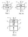
- FIG. 1is a cross-sectional schematic diagram of an illustrative magnetic tunnel junction cell with in-plane magnetization orientation
- FIG. 1Ais a cross-sectional schematic diagram of an illustrative perpendicular anisotropy magnetic tunnel junction cell with out-of-plane magnetization orientation
- FIG. 2is a cross-sectional schematic diagram of a perpendicular anisotropy magnetic tunnel junction cell having a stress-assisted switch with the switch in the “off” state;
- FIG. 3is a schematic diagram of a memory device including the magnetic tunnel junction cell of FIG. 2 ;
- FIG. 4is a cross-sectional schematic diagram of the magnetic tunnel junction cell of FIG. 2 with a stress being applied to change the phase-change material from its antiferromagnetic state to its ferromagnetic state;
- FIG. 5Ais a cross-sectional schematic diagram of the magnetic tunnel junction cell of FIG. 2 with a switching current applied in a first direction thereto;
- FIG. 5Bis a cross-sectional schematic diagram of the magnetic tunnel junction cell of FIG. 2 with a switching current applied in a second direction thereto;
- FIG. 6is a flow chart of a method for forming a magnetic tunnel junction cell, such as the cell of FIG. 2 ;
- FIG. 7is a flow chart of a method for using a memory device, such as the memory device of FIG. 3 .
- spin-transfer torque memoryalso referred to as spin torque memory, spin torque RAM, or STRAM
- spin torque RAMspin torque RAM
- STRAMspin torque RAM
- MTJsmagnetic tunnel junction cells
- the spin magnetic tunnel junction cells (MTJs) of this disclosureutilize a mechanical strain to assist in the switching of the magnetization orientation of the free layer of the magnetic tunnel junction cell. Nano-mechanical tensile stress is applied to a phase-change material layer within the magnetic tunnel junction cell to increase the lattice parameters to activate the phase change and orient the layer magnetization.
- FIG. 1is a cross-sectional schematic diagram of a magnetic tunnel junction cell 10 that includes a soft ferromagnetic free layer 12 and a ferromagnetic reference (i.e., pinned) layer 14 .
- Ferromagnetic free layer 12 and ferromagnetic pinned layer 14are separated by an oxide barrier layer 13 or non-magnetic tunnel barrier. Note that other layers, such as seed or capping layers, are not depicted for clarity.
- Ferromagnetic layers 12 , 14may be made of any useful ferromagnetic (FM) material such as, for example, Fe, Co or Ni and alloys thereof, such as NiFe and CoFe. Ternary alloys, such as CoFeB, may be particularly useful because of their lower moment and high polarization ratio, which are desirable for the spin-current switch.
- Either or both of free layer 12 and pinned layer 14may be either a single layer or a synthetic antiferromagnetic (SAF) coupled structure, i.e., two ferromagnetic sublayers separated by a metallic spacer, such as Ru or Cu, with the magnetization orientations of the sublayers in opposite directions to provide a net magnetization.
- SAFsynthetic antiferromagnetic
- the magnetization orientation of ferromagnetic free layer 12is more readily switchable than the magnetization orientation of ferromagnetic pinned layer 14 .
- Barrier layer 13may be made of an electrically insulating material such as, for example an oxide material (e.g., Al 2 O 3 , TiO x or MgO). Other suitable materials may also be used. Barrier layer 13 could optionally be patterned with free layer 12 or with pinned layer 14 , depending on process feasibility and device reliability.
- oxide barrier layer 13includes Ta 2 O 5 (for example, at a thickness of about 0.5 to 1 nanometer) and ferromagnetic free layer 12 and a ferromagnetic pinned layer 14 include NiFe, CoFe, or Co.
- barrier layer 13includes GaAs (for example, at a thickness of about 5 to 15 nanometers) and ferromagnetic free layer 12 and ferromagnetic pinned layer 14 include Fe.
- barrier layer 13includes Al 2 O 3 (for example, a few (e.g., about 1-5) nanometers thick) and ferromagnetic free layer 12 and ferromagnetic pinned layer 14 include NiFe, CoFe, or Co.
- a first electrode 18is in electrical contact with ferromagnetic free layer 12 and a second electrode 19 is in electrical contact with ferromagnetic pinned layer 14 .
- Electrodes 18 , 19electrically connect ferromagnetic layers 12 , 14 to a control circuit providing read and write currents through layers 12 , 14 .
- the resistance across magnetic tunnel junction cell 10is determined by the relative orientation of the magnetization vectors or magnetization orientations of ferromagnetic layers 12 , 14 .
- the magnetization direction of ferromagnetic pinned layer 14is pinned in a predetermined direction while the magnetization direction of ferromagnetic free layer 12 is free to rotate under the influence of spin torque.
- Pinning of ferromagnetic pinned layer 14may be achieved through, e.g., the use of exchange bias with an antiferromagnetically ordered material such as PtMn, IrMn, and others.
- magnetic tunnel junction cell 10is in the low resistance state where the magnetization orientation of ferromagnetic free layer 12 is parallel and in the same direction of the magnetization orientation of ferromagnetic pinned layer 14 . This is termed the low resistance state or “0” data state.
- magnetic tunnel junction cell 10is in the high resistance state where the magnetization orientation of ferromagnetic free layer 12 is anti-parallel and in the opposite direction of the magnetization orientation of ferromagnetic pinned layer 14 . This is termed the high resistance state or “1” data state.
- Free layer 12is where data or bit information is stored when the device operates under “read”, or overwritten when the device operates under “write”.
- Each ferromagnetic layer 12 , 14acts as “spin filter” when cell 10 writes with “0” or “1” as the switching current passes through in opposite directions to alter magnetization of free layer 12 .
- FIG. 1Aillustrates an alternate embodiment of a magnetic tunnel junction cell that has the magnetization orientations of the free layer and the pinned layer perpendicular to the plane of the layers, or out-of-plane.
- magnetic tunnel junction cell 10 A of FIG. 1Ahas soft ferromagnetic free layer 12 A and a ferromagnetic reference (i.e., pinned) layer 14 A separated by an oxide barrier layer 13 A or non-magnetic tunnel barrier.
- a first electrode 18 Ais in electrical contact with ferromagnetic free layer 12 A and a second electrode 19 A is in electrical contact with ferromagnetic pinned layer 14 A.
- Other layers, such as seed or capping layers,are not depicted for clarity.
- Electrodes 18 A, 19 Aelectrically connect ferromagnetic layers 12 A, 14 A to a control circuit providing read and write currents through layers 12 A, 14 A.
- the various elements of cell 10 Aare similar to the element of cell 10 , described above, except that the magnetization orientations of layers 12 A, 14 A are oriented perpendicular to the layer extension rather than in the layer plane.
- Free layer 12 A and pinned layer 14 Aeach have a magnetization orientation associated therewith, illustrated in FIG. 1A .
- magnetic tunnel junction cell 10 Ais in the low resistance state or “0” data state where the magnetization orientation of free layer 12 A is in the same direction of the magnetization orientation of pinned layer 14 A.
- magnetic tunnel junction cell 10 Ais in the high resistance state or “1” data state where the magnetization orientation of free layer 12 A is in the opposite direction of the magnetization orientation of pinned layer 14 A.
- switching the resistance state and hence the data state of magnetic tunnel junction cell 10 A via spin-transferoccurs when a current, passing through a magnetic layer of magnetic tunnel junction cell 10 A, becomes spin polarized and imparts a spin torque on free layer 12 A.
- a sufficient spin torqueis applied to free layer 12 A, the magnetization orientation of free layer 12 A can be switched between two opposite directions and accordingly, magnetic tunnel junction cell 10 A can be switched between the low resistance state or “0” data state and the high resistance state or “1” data state.
- the switching of the free layer magnetization orientationis facilitated by a coupling layer proximate the free layer.
- the coupling layerhas a phase change material, which, upon its phase change, destabilizes the free layer and reduces the switching current needed.
- the phase change material of the coupling layeris incited to phase change by mechanical stress or strain.
- Magnetic tunnel junction cell 20includes a soft perpendicular ferromagnetic free layer 22 and a perpendicular ferromagnetic reference (i.e., pinned) layer 24 . Ferromagnetic free layer 22 and ferromagnetic pinned layer 24 are separated by an oxide barrier layer 23 or non-magnetic tunnel barrier. The magnetization orientation of layer 22 , 24 is perpendicular to the layer, or, out-of-plane.
- Non-limiting examples of suitable materials for these layersinclude: for free layer 22 , a thin layer (e.g., about 2-30 nm) of Co/Pt multilayers or FePt alloys or CoFe/Pt or CoFeX where X is a rare-earth transition metal such as Tb or Gd; for pinned layer 24 , a thick layer (e.g., about 5-50 nm) of Co/Pt multilayers or FePt alloys or CoFePt or CoFeX; for barrier 23 , insulating material (e.g., about 10-30 Angstroms) such as Al 2 O 3 or MgO.
- free layer 22 , pinned layer 24 and barrier layer 23could be any of the materials described above in relation to free layer 12 , 12 A, pinned layer 14 , 14 A or barrier layer 13 , 13 A.
- magnetic tunnel junction cell 20also includes a second ferromagnetic pinned layer 26 and a phase change material coupling layer 25 positioned between free layer 22 and second pinned layer 26 .
- Coupling layer 25may be adjacent to one or both of free layer 22 and pinned layer 26 or may have an intermediate layer therebetween.
- Second pinned layer 26can have properties similar to pinned layer 24 , or any of the properties or characteristics discussed above in relation to pinned layer 14 of cell 10 or pinned layer 14 A of cell 10 A.
- second pinned layer 26 and coupling layer 25have magnetization orientations that are in the plane of the layers, or, in-plane.
- Coupling layer 25is formed of a phase change material, which changes a physical property upon an activating incident, such as being exposed to a voltage.
- Coupling layer 25may be formed from an antiferromagnetic or superparamagnetic phase transition material that can change to a ferromagnetic material upon an activating incident.
- a non-limiting example of a suitable phase change material that transitions from magnetic to antimagnetic and backis FeRh and ternary alloys thereof, such as FeRhIr and FeRhPt.
- Second pinned layer 26provides directional pinning of coupling layer 25 when coupling layer 25 is in its magnetic state.
- Magnetic tunnel junction cell 20has a first electrode 28 in electrical contact with second ferromagnetic pinned layer 26 and a second electrode 29 in electrical contact with ferromagnetic pinned layer 24 .
- Electrodes 28 , 29are formed of an electrically conducting material, typically metal. An example of a suitable metal for electrodes 28 , 29 is Pt. Electrodes 28 , 29 electrically connect ferromagnetic layers 22 , 24 , 26 and coupling layer 25 to a control circuit.
- the illustrative spin-transfer torque magnetic tunnel junction cell 20may be used to construct a memory device where a data bit is stored in the magnetic tunnel junction cell by the relative magnetization state of free layer 22 with respect to pinned layer 24 .
- the stored data bitcan be read out by measuring the resistance of cell 20 which changes with the magnetization direction of free layer 22 relative to pinned layer 24 .
- FIG. 3illustrates magnetic tunnel junction cell 20 incorporated into a memory device 30 with a transistor and control circuit.
- Tunnel junction cell 20having free layer 22 , barrier 23 , pinned layers 24 , 26 and coupling layer 25 , is connected to bit line BL via electrode 28 and to word line WL via electrode 29 and transistor 33 .
- Proximate tunnel junction cell 20is at least one actuator electrode 31 , in this embodiment, first and second actuator electrodes 31 A, 31 B.
- Electrode 31e.g., actuator electrodes 31 A, 31 B, is present proximate at least coupling layer 25 and optionally proximate one or more of free layer 22 , pinned layer 24 , and second pinned layer 26 .
- Electrode(s) 31may be formed of a piezoelectric material or a magnetoelectric material.
- An example of a suitable piezoelectric material for electrode(s) 31is lead zirconate titanate (PbZrTiO).
- Actuator electrode(s) 31are connected to receive a voltage therethrough, for example, from a timing circuit control 35 . The voltage through electrode(s) 31 may be coincident with write voltage passed through cell 20 to write or switch free layer 22 .
- Actuator electrode(s) 31initiate stress and strain that is relayed or transferred to coupling layer 25 .
- the voltageinduces a nano-mechanical strain in electrode(s) 31 which transfers to the proximate coupling layer 25 .
- This strain on the phase change material of coupling layer 25increases the lattice parameters of the material to activate a switch change from its antiferromagnetic (AF) state to ferromagnetic (F) state in the applied stress direction.
- AFantiferromagnetic
- Fferromagnetic
- the AF-F state transitionoccurs when the FeRh lattice constant changes (under increasing temperature) about 0.3%-0.5%.
- FeRh having a Young's modulus ⁇ FeRh1.7 ⁇ 10 11 Pa, only approximately a few volts or less are needed to generate the 0.3%-0.5% strain level.
- the actuation voltage sourcecan be shared with the address signal to synchronize the “write” or switching event through a simple RC delay circuitry; such as timing circuit control 35 .
- I d⁇ ⁇ ⁇ eM s ⁇ ⁇ V ⁇ ⁇ ⁇ g ⁇ [ H k - H eff ]
- H effH ex + H + 4 ⁇ ⁇ ⁇ ⁇ ⁇ M s
- M s and H kare respectively magnetization and anisotropy field of the free layer, and H is the perpendicular field.
- I d⁇ ⁇ ⁇ eM s ⁇ V ⁇ ⁇ ⁇ g ⁇ [ H k - 4 ⁇ ⁇ ⁇ ⁇ ⁇ M s ]
- H ex0
- H effthe exchange field from the phase change material (e.g., FeRh) in the ferromagnetic state. H ex is thus determined by:
- a voltageis needed for actuator electrode(s) 31 to induce the magnetic phase transition of coupling layer 25 .
- the voltageis determined by:
- V⁇ ⁇ ⁇ L ⁇ ⁇ ⁇ ⁇ DS 33
- E Ld 33⁇ ⁇ ⁇ ⁇ ⁇ DS 33 E d 33
- a design such as memory device 30with magnetic tunnel junction cell 20 having a phase change coupling layer 25 and actuator electrode(s) 31 , has numerous design advantages over memory devices that have a conventional magnetic tunnel junction cell or that have a magnetic tunnel junction cell that utilizes other methods to facilitate switching of the free layer.
- the switching current in needed to switch the free layeris less than about 10% of that needed when no free layer instability is present.
- other advantagesexist. For example, by using a coupling layer that has a phase change that is strain activated, there is no need to heat the coupling layer or the free layer, so that the design is more thermally reliable than other designs.
- the AF-F switch and the subsequent free layer switchingcan be precisely controlled. This AF-F switching is fast and efficient, with the transition from AF-F and from F-AF being in the range of femto seconds, with no hysteresis.
- the operation mechanism of cell 20in particular the switching process of the magnetization orientation of free layer 22 is a 2-step process.
- the phase change material of coupling layer 25is initially in its antiferromagnetic state, with an undefined magnetization orientation in relation to second pinned layer 26 .
- Both pinned layer 24 and free layer 22have a perpendicular or out-of-plane magnetization orientation, with the magnetization of free layer 22 being undefined as to orientation (e.g., either the same or opposite direction and the magnetization orientation of pinned layer 24 ).
- An interfaceexists between free layer 22 and coupling layer 25 .
- the voltage to actuator electrode(s) 31(in FIG. 3 ) is switched “ON”.
- the voltage in electrode(s) 31causes a stress or strain in electrode(s) 31 , which is applied to coupling layer 25 .
- the stress on coupling layer 25causes the phase change material to switch from its antiferromagnetic (AF) stage to its ferromagnetic (F) state and orient itself with the magnetization orientation of second pinning layer 26 , illustrated in FIG. 4 .
- the exchange field between free layer 22 and coupling layer 25reduces the stability of free layer 22 ; the instability in free layer 22 shown in FIG. 4 .
- spin current Iis passed through magnetic tunnel junction cell 20 via electrodes 28 , 29 ( FIG. 2 ) in the direction from free layer 22 to pinned layer 24 .
- the spin currentis removed, as is the voltage to electrode(s) 31 .
- the resulting free layer stabilityis restored to the original thermal stability, approximately 0.5M S V(H k -47 ⁇ M s ), and the resulting magnetization orientation is retained.
- spin current Iis passed through magnetic tunnel junction cell 20 via electrodes 28 , 29 ( FIG. 2 ) in the direction from pinned layer 24 to free layer 22 .
- the spin currentis removed, as is the voltage to electrode(s) 31 .
- the resulting free layer stabilityis restored to its original thermal stability, approximately 0.5M s V(H k -47 ⁇ M s ), and the resulting magnetization orientation is retained.
- the magnetic tunnel junction cell (e.g., cell 20 ) and memory structures (e.g., memory device 30 ) of this disclosuremay be made by well-known thin film building and removal techniques such as chemical vapor deposition (CVD), physical vapor deposition (PVD), atomic layer deposition (ALD), photolithography, dry etching, wet etching, or ion milling.
- the magnetization orientations of the pinned layer(s)e.g., layers 24 , 26
- the actuator electrode(s)may be formed using well-known thin film techniques or may be previously formed and connected to the cell.
- FIG. 6illustrates stepwise a method for making magnetic tunnel junction 20 or other magnetic tunnel junction cell that utilizes a mechanical strain to assist in the switching of the magnetization orientation of the free layer.
- Method 100includes Step 101 of forming a magnetic tunnel junction having a phase change coupling layer proximate the free layer (e.g., forming cell 20 having coupling layer 25 proximate free layer 22 ).
- Step 103 of the methodincludes providing at least one actuator electrode proximate at least the coupling layer (e.g., providing actuator electrode(s) 31 proximate at least coupling layer 25 ).
- the actuator electrode(s)are electrically connected to a voltage source to apply voltage through the electrodes.
- FIG. 7illustrates stepwise a method for writing a data state to magnetic tunnel junction cell 20 or other magnetic tunnel junction cell that utilizes a mechanical strain to assist in the switching of the magnetization orientation of the free layer.
- Nano-mechanical tensile stressis applied to a phase-change material layer within the magnetic tunnel junction cell to increase the lattice parameters to activate the phase change and orient the layer magnetization.
- Method 110includes starting at 111 with a magnetic tunnel junction cell (e.g., cell 20 ) with its phase change coupling layer (e.g., coupling layer 25 ) in the antiferromagnetic state.
- the voltage to actuator electrode(s)e.g., electrode(s) 31 in FIG. 3
- the phase change coupling layere.g., coupling layer 25
- the stress on the coupling layercauses the phase change material to switch from its antiferromagnetic (AF) stage to its ferromagnetic (F) state, in Step 114 A.
- Step 114 BThe exchange field between the coupling layer and the proximate free layer (e.g., free layer 22 ) reduces the stability of the free layer facilitating orienting the magnetization of that layer; Step 114 B.
- Step 115spin current is turned ON and passed through the magnetic tunnel junction cell (e.g., cell 20 ). This current orients the free layer magnetization (Step 116 ) to either the same direction or the opposite direction as of the corresponding pinned layer (e.g., pinned layer 24 ).
- Step 117the spin current is turned OFF, and the voltage to the electrode(s) is turned OFF.
- the resistance state of the magnetic tunnel junction cellis determined in Step 119 ; the resistance state will be either “0” or “1”.
Landscapes
- Engineering & Computer Science (AREA)
- Chemical & Material Sciences (AREA)
- Nanotechnology (AREA)
- Crystallography & Structural Chemistry (AREA)
- Physics & Mathematics (AREA)
- Power Engineering (AREA)
- Computer Hardware Design (AREA)
- Manufacturing & Machinery (AREA)
- General Physics & Mathematics (AREA)
- Condensed Matter Physics & Semiconductors (AREA)
- Spectroscopy & Molecular Physics (AREA)
- Hall/Mr Elements (AREA)
- Mram Or Spin Memory Techniques (AREA)
Abstract
Description
where δSLis the free layer thickness of
Claims (24)
Priority Applications (2)
| Application Number | Priority Date | Filing Date | Title |
|---|---|---|---|
| US12/248,237US8054677B2 (en) | 2008-08-07 | 2008-10-09 | Magnetic memory with strain-assisted exchange coupling switch |
| US13/271,302US8406042B2 (en) | 2008-08-07 | 2011-10-12 | Magnetic memory with strain-assisted exchange coupling switch |
Applications Claiming Priority (2)
| Application Number | Priority Date | Filing Date | Title |
|---|---|---|---|
| US8687308P | 2008-08-07 | 2008-08-07 | |
| US12/248,237US8054677B2 (en) | 2008-08-07 | 2008-10-09 | Magnetic memory with strain-assisted exchange coupling switch |
Related Child Applications (1)
| Application Number | Title | Priority Date | Filing Date |
|---|---|---|---|
| US13/271,302ContinuationUS8406042B2 (en) | 2008-08-07 | 2011-10-12 | Magnetic memory with strain-assisted exchange coupling switch |
Publications (2)
| Publication Number | Publication Date |
|---|---|
| US20100032738A1 US20100032738A1 (en) | 2010-02-11 |
| US8054677B2true US8054677B2 (en) | 2011-11-08 |
Family
ID=41652084
Family Applications (2)
| Application Number | Title | Priority Date | Filing Date |
|---|---|---|---|
| US12/248,237Expired - Fee RelatedUS8054677B2 (en) | 2008-08-07 | 2008-10-09 | Magnetic memory with strain-assisted exchange coupling switch |
| US13/271,302Expired - Fee RelatedUS8406042B2 (en) | 2008-08-07 | 2011-10-12 | Magnetic memory with strain-assisted exchange coupling switch |
Family Applications After (1)
| Application Number | Title | Priority Date | Filing Date |
|---|---|---|---|
| US13/271,302Expired - Fee RelatedUS8406042B2 (en) | 2008-08-07 | 2011-10-12 | Magnetic memory with strain-assisted exchange coupling switch |
Country Status (1)
| Country | Link |
|---|---|
| US (2) | US8054677B2 (en) |
Cited By (11)
| Publication number | Priority date | Publication date | Assignee | Title |
|---|---|---|---|---|
| US20100109111A1 (en)* | 2008-10-30 | 2010-05-06 | Kyung Ho Shin | Magnetic tunnel junction structure having free layer with oblique magnetization |
| US20110007431A1 (en)* | 2009-06-25 | 2011-01-13 | Hitachi Global Storage Technologies Netherlands .B. V. | Spin torque oscillator sensor enhanced by magnetic anisotropy |
| US20110058412A1 (en)* | 2009-04-28 | 2011-03-10 | Seagate Technology Llc | Magnetic stack having assist layer |
| US20110147709A1 (en)* | 2009-12-22 | 2011-06-23 | Globalfoundries Inc. | Signal control elements in ferromagnetic logic |
| US20120281460A1 (en)* | 2011-05-03 | 2012-11-08 | International Business Machines Corporation | Noncontact writing of nanometer scale magnetic bits using heat flow induced spin torque effect |
| US20120292723A1 (en)* | 2011-05-20 | 2012-11-22 | Agency For Science, Technology And Research | Magnetoresistive Device |
| US8406045B1 (en)* | 2011-01-19 | 2013-03-26 | Grandis Inc. | Three terminal magnetic element |
| US8456895B2 (en) | 2011-05-03 | 2013-06-04 | International Business Machines Corporation | Magnonic magnetic random access memory device |
| WO2013101203A1 (en)* | 2011-12-30 | 2013-07-04 | Intel Corporation | Balancing energy barrier between states in perpendicular magnetic tunnel junctions |
| US8754491B2 (en) | 2011-05-03 | 2014-06-17 | International Business Machines Corporation | Spin torque MRAM using bidirectional magnonic writing |
| US9960207B1 (en)* | 2016-10-13 | 2018-05-01 | Globalfoundries Inc. | Spin-selective electron relay |
Families Citing this family (28)
| Publication number | Priority date | Publication date | Assignee | Title |
|---|---|---|---|---|
| US8487390B2 (en)* | 2008-10-08 | 2013-07-16 | Seagate Technology Llc | Memory cell with stress-induced anisotropy |
| US20100091564A1 (en)* | 2008-10-10 | 2010-04-15 | Seagate Technology Llc | Magnetic stack having reduced switching current |
| US9165625B2 (en)* | 2008-10-30 | 2015-10-20 | Seagate Technology Llc | ST-RAM cells with perpendicular anisotropy |
| US8053255B2 (en)* | 2009-03-03 | 2011-11-08 | Seagate Technology Llc | STRAM with compensation element and method of making the same |
| KR101766899B1 (en) | 2010-04-21 | 2017-08-10 | 삼성전자주식회사 | Magnetic Memory Device |
| US9299923B2 (en)* | 2010-08-24 | 2016-03-29 | Samsung Electronics Co., Ltd. | Magnetic devices having perpendicular magnetic tunnel junction |
| KR102017622B1 (en)* | 2012-08-21 | 2019-09-03 | 삼성전자주식회사 | Magnetic memory devices having perpendicular magnetic tunnel junction |
| US8907436B2 (en)* | 2010-08-24 | 2014-12-09 | Samsung Electronics Co., Ltd. | Magnetic devices having perpendicular magnetic tunnel junction |
| EP2538235B1 (en)* | 2011-06-24 | 2013-07-31 | Christian-Albrechts-Universität zu Kiel | Magnetostrictive layer system |
| EP2541554B1 (en)* | 2011-06-30 | 2015-12-30 | Hitachi, Ltd. | Magnetic functional device |
| WO2013020569A1 (en) | 2011-08-10 | 2013-02-14 | Christian-Albrechts-Universität Zu Kiel | Magnetoresistive memory with low critical current for magnetization switching |
| US8704320B2 (en) | 2011-09-12 | 2014-04-22 | Qualcomm Incorporated | Strain induced reduction of switching current in spin-transfer torque switching devices |
| US20140028897A1 (en)* | 2012-07-25 | 2014-01-30 | Digitaloptics Corporation | Camera Orientation Sensing Using Camera Module Processor |
| US9076953B2 (en) | 2012-05-09 | 2015-07-07 | Qualcomm Incorporated | Spin transistors employing a piezoelectric layer and related memory, memory systems, and methods |
| US9013916B2 (en)* | 2012-05-31 | 2015-04-21 | Northrop Grumman Systems Corporation | Josephson magnetic memory cell system |
| JP2014049497A (en)* | 2012-08-29 | 2014-03-17 | Toshiba Corp | Nonvolatile semiconductor storage device and operation method of the same |
| US10270003B2 (en)* | 2012-12-04 | 2019-04-23 | Taiwan Semiconductor Manufacturing Company, Ltd. | Method and apparatus for CMOS sensor packaging |
| EP3198598A4 (en)* | 2014-09-25 | 2018-07-18 | Intel Corporation | Strain assisted spin torque switching spin transfer torque memory |
| JP6424272B2 (en)* | 2015-06-03 | 2018-11-14 | 国立研究開発法人科学技術振興機構 | Magnetoresistive element and memory circuit |
| WO2017034564A1 (en)* | 2015-08-26 | 2017-03-02 | Intel Corporation | Single pulse magneto-strictive switching via hybrid magnetization stack |
| DE102016004816A1 (en) | 2016-04-21 | 2017-10-26 | Universität Kassel | Magnetoelectric memory for storing digital data |
| CN109507616A (en)* | 2017-09-14 | 2019-03-22 | 中国科学院宁波材料技术与工程研究所 | Characterizing method that antiferromagnet changes in stress magnetic, characterization device and preparation method thereof |
| CN109244233B (en)* | 2018-07-26 | 2021-02-19 | 西安交通大学 | Magnetic tunnel junction device based on artificial antiferromagnetic fixed layer and random storage device |
| CN112133343B (en)* | 2019-06-25 | 2022-08-23 | 中电海康集团有限公司 | Magnetic memory cell and magnetic memory |
| CN112259139B (en)* | 2019-07-22 | 2022-09-30 | 中电海康集团有限公司 | Memory cell, memory, and method for initializing memory |
| EP3940702B1 (en)* | 2020-07-14 | 2024-11-27 | Universitat Autònoma de Barcelona | A magnetoelectric device and uses of the magnetoelectric device |
| CN116133439A (en)* | 2022-09-09 | 2023-05-16 | 长江存储科技有限责任公司 | Semiconductor structure, preparation method thereof, three-dimensional memory and memory system |
| US20250287608A1 (en)* | 2024-03-08 | 2025-09-11 | International Business Machines Corporation | Pillar critical dimension reduction by isotropic plasma etching with high selectivity to silicon-containing antireflective coating and silicon nitride |
Citations (116)
| Publication number | Priority date | Publication date | Assignee | Title |
|---|---|---|---|---|
| US5461526A (en) | 1992-03-24 | 1995-10-24 | Hitachi, Ltd. | Magnetoresistive read head and magnetic storage system using the same |
| US5841692A (en) | 1996-03-18 | 1998-11-24 | International Business Machines Corporation | Magnetic tunnel junction device with antiferromagnetically coupled pinned layer |
| US5963472A (en) | 1994-12-27 | 1999-10-05 | Nkk Corporation | Information storage apparatus and method for operating the same |
| US6146775A (en)* | 1996-11-18 | 2000-11-14 | Sanyo Electric Co., Ltd. | Magnetoresistive film |
| US6166948A (en) | 1999-09-03 | 2000-12-26 | International Business Machines Corporation | Magnetic memory array with magnetic tunnel junction memory cells having flux-closed free layers |
| US6183859B1 (en) | 1998-07-20 | 2001-02-06 | Motorola, Inc | Low resistance MTJ |
| US6185080B1 (en)* | 1999-03-29 | 2001-02-06 | International Business Machines Corporation | Dual tunnel junction sensor with a single antiferromagnetic layer |
| US20020186582A1 (en) | 2001-04-02 | 2002-12-12 | Manish Sharma | Cladded read conductor for a pinned-on-the-fly soft reference layer |
| US6522573B2 (en) | 2000-06-30 | 2003-02-18 | Kabushiki Kaisha Toshiba | Solid-state magnetic memory using ferromagnetic tunnel junctions |
| US6597618B2 (en) | 2001-12-04 | 2003-07-22 | Data Storage Institute | Magnetic tunnel junction magnetic random access memory |
| US6605772B2 (en) | 1999-08-27 | 2003-08-12 | Massachusetts Institute Of Technology | Nanostructured thermoelectric materials and devices |
| US6633498B1 (en) | 2002-06-18 | 2003-10-14 | Motorola, Inc. | Magnetoresistive random access memory with reduced switching field |
| US6714444B2 (en) | 2002-08-06 | 2004-03-30 | Grandis, Inc. | Magnetic element utilizing spin transfer and an MRAM device using the magnetic element |
| US20040084702A1 (en) | 2002-11-01 | 2004-05-06 | Won-Cheol Jeong | Magnetic memories with bit lines and digit lines that intersect at oblique angles and fabrication methods thereof |
| US6771534B2 (en) | 2002-11-15 | 2004-08-03 | International Business Machines Corporation | Thermally-assisted magnetic writing using an oxide layer and current-induced heating |
| US6781874B2 (en) | 2001-08-02 | 2004-08-24 | Renesas Technology Corp. | Thin film magnetic memory device including memory cells having a magnetic tunnel junction |
| US6791865B2 (en) | 2002-09-03 | 2004-09-14 | Hewlett-Packard Development Company, L.P. | Memory device capable of calibration and calibration methods therefor |
| US6819586B1 (en) | 2003-10-24 | 2004-11-16 | Hewlett-Packard Development Company, L.P. | Thermally-assisted magnetic memory structures |
| US6829161B2 (en) | 2003-01-10 | 2004-12-07 | Grandis, Inc. | Magnetostatically coupled magnetic elements utilizing spin transfer and an MRAM device using the magnetic element |
| US6838740B2 (en) | 2002-09-27 | 2005-01-04 | Grandis, Inc. | Thermally stable magnetic elements utilizing spin transfer and an MRAM device using the magnetic element |
| US6845038B1 (en) | 2003-02-01 | 2005-01-18 | Alla Mikhailovna Shukh | Magnetic tunnel junction memory device |
| US6847547B2 (en) | 2003-02-28 | 2005-01-25 | Grandis, Inc. | Magnetostatically coupled magnetic elements utilizing spin transfer and an MRAM device using the magnetic element |
| US20050018475A1 (en) | 2003-07-22 | 2005-01-27 | Lung Tran | Magnetic memory structure |
| US6888742B1 (en) | 2002-08-28 | 2005-05-03 | Grandis, Inc. | Off-axis pinned layer magnetic element utilizing spin transfer and an MRAM device using the magnetic element |
| US20050104146A1 (en) | 2003-11-14 | 2005-05-19 | Nickel Janice H. | Thin film device and a method of providing thermal assistance therein |
| US6903400B2 (en) | 2003-10-06 | 2005-06-07 | Fujitsu Limited | Magnetoresistive memory apparatus |
| US20050150535A1 (en) | 2004-01-13 | 2005-07-14 | Nanocoolers, Inc. | Method for forming a thin-film thermoelectric device including a phonon-blocking thermal conductor |
| US20050150537A1 (en) | 2004-01-13 | 2005-07-14 | Nanocoolers Inc. | Thermoelectric devices |
| US6933155B2 (en) | 2003-05-21 | 2005-08-23 | Grandis, Inc. | Methods for providing a sub .15 micron magnetic memory structure |
| US6950335B2 (en) | 2001-11-16 | 2005-09-27 | Commissariat A L'energie Atomique | Magnetic tunnel junction magnetic device, memory and writing and reading methods using said device |
| US20050213375A1 (en) | 2004-03-23 | 2005-09-29 | Perner Frederick A | Soft-reference three conductor magnetic memory storage device |
| US6958927B1 (en) | 2002-10-09 | 2005-10-25 | Grandis Inc. | Magnetic element utilizing spin-transfer and half-metals and an MRAM device using the magnetic element |
| US6963098B2 (en) | 2003-06-23 | 2005-11-08 | Nve Corporation | Thermally operated switch control memory cell |
| US6967863B2 (en) | 2004-02-25 | 2005-11-22 | Grandis, Inc. | Perpendicular magnetization magnetic element utilizing spin transfer |
| US6980464B2 (en) | 2002-09-10 | 2005-12-27 | Kabushiki Kaisha Toshiba | Magnetic random access memory |
| US6980469B2 (en) | 2003-08-19 | 2005-12-27 | New York University | High speed low power magnetic devices based on current induced spin-momentum transfer |
| US6985385B2 (en) | 2003-08-26 | 2006-01-10 | Grandis, Inc. | Magnetic memory element utilizing spin transfer switching and storing multiple bits |
| US7006336B2 (en) | 2002-08-06 | 2006-02-28 | International Business Machines Corporation | Magnetic head having a heater circuit for thermally-assisted writing |
| US7020009B2 (en) | 2003-05-14 | 2006-03-28 | Macronix International Co., Ltd. | Bistable magnetic device using soft magnetic intermediary material |
| US7031178B2 (en) | 2003-06-10 | 2006-04-18 | International Business Machines Corporation | Magnetic shift register with shiftable magnetic domains between two regions, and method of using the same |
| US7057921B2 (en) | 2004-05-11 | 2006-06-06 | Grandis, Inc. | Spin barrier enhanced dual magnetoresistance effect element and magnetic memory using the same |
| US7088609B2 (en) | 2004-05-11 | 2006-08-08 | Grandis, Inc. | Spin barrier enhanced magnetoresistance effect element and magnetic memory using the same |
| US7098494B2 (en) | 2004-06-16 | 2006-08-29 | Grandis, Inc. | Re-configurable logic elements using heat assisted magnetic tunneling elements |
| US7110287B2 (en) | 2004-02-13 | 2006-09-19 | Grandis, Inc. | Method and system for providing heat assisted switching of a magnetic element utilizing spin transfer |
| US20060215444A1 (en) | 2005-03-24 | 2006-09-28 | Perner Frederick A | Series diode thermally assisted MRAM |
| US7126202B2 (en) | 2004-11-16 | 2006-10-24 | Grandis, Inc. | Spin scattering and heat assisted switching of a magnetic element |
| US7160770B2 (en) | 1998-07-17 | 2007-01-09 | Murata Manufacturing Co., Ltd. | Method of manufacturing an electronic component including an inter-line insulating layer and a conductor pattern |
| US7161829B2 (en) | 2003-09-19 | 2007-01-09 | Grandis, Inc. | Current confined pass layer for magnetic elements utilizing spin-transfer and an MRAM device using such magnetic elements |
| US20070034919A1 (en) | 2005-08-09 | 2007-02-15 | Maglc Technologies, Inc. | MRAM with super-paramagnetic sensing layer |
| US7180113B2 (en) | 2005-02-10 | 2007-02-20 | Infineon Technologies Ag | Double-decker MRAM cell with rotated reference layer magnetizations |
| US7187577B1 (en) | 2005-11-23 | 2007-03-06 | Grandis, Inc. | Method and system for providing current balanced writing for memory cells and magnetic devices |
| US7190611B2 (en) | 2003-01-07 | 2007-03-13 | Grandis, Inc. | Spin-transfer multilayer stack containing magnetic layers with resettable magnetization |
| US7205564B2 (en) | 2003-11-11 | 2007-04-17 | Kabushiki Kaisha Toshiba | Resistance change memory having organic semiconductor layer |
| US20070085068A1 (en) | 2005-10-14 | 2007-04-19 | Dmytro Apalkov | Spin transfer based magnetic storage cells utilizing granular free layers and magnetic memories using such cells |
| US7224601B2 (en) | 2005-08-25 | 2007-05-29 | Grandis Inc. | Oscillating-field assisted spin torque switching of a magnetic tunnel junction memory element |
| US7230265B2 (en) | 2005-05-16 | 2007-06-12 | International Business Machines Corporation | Spin-polarization devices using rare earth-transition metal alloys |
| US7230845B1 (en) | 2005-07-29 | 2007-06-12 | Grandis, Inc. | Magnetic devices having a hard bias field and magnetic memory devices using the magnetic devices |
| US7233039B2 (en) | 2004-04-21 | 2007-06-19 | Grandis, Inc. | Spin transfer magnetic elements with spin depolarization layers |
| US7241631B2 (en) | 2004-12-29 | 2007-07-10 | Grandis, Inc. | MTJ elements with high spin polarization layers configured for spin-transfer switching and spintronics devices using the magnetic elements |
| US7242045B2 (en) | 2004-02-19 | 2007-07-10 | Grandis, Inc. | Spin transfer magnetic element having low saturation magnetization free layers |
| US7242048B2 (en) | 2003-12-22 | 2007-07-10 | Grandis, Inc. | Magnetic elements with ballistic magnetoresistance utilizing spin-transfer and an MRAM device using such magnetic elements |
| US7245462B2 (en) | 2003-08-21 | 2007-07-17 | Grandis, Inc. | Magnetoresistive element having reduced spin transfer induced noise |
| US20070176251A1 (en) | 2006-01-27 | 2007-08-02 | Se-Chung Oh | Magnetic memory device and method of fabricating the same |
| US7252852B1 (en) | 2003-12-12 | 2007-08-07 | International Business Machines Corporation | Mg-Zn oxide tunnel barriers and method of formation |
| US7272034B1 (en) | 2005-08-31 | 2007-09-18 | Grandis, Inc. | Current driven switching of magnetic storage cells utilizing spin transfer and magnetic memories using such cells |
| US7272035B1 (en) | 2005-08-31 | 2007-09-18 | Grandis, Inc. | Current driven switching of magnetic storage cells utilizing spin transfer and magnetic memories using such cells |
| US7274057B2 (en) | 2004-04-26 | 2007-09-25 | International Business Machines Corporation | Techniques for spin-flop switching with offset field |
| US7277259B2 (en)* | 2003-02-07 | 2007-10-02 | Alps Electric Co., Ltd. | Magnetic head actuator including piezoelectric elements fixed to the arms of a fired glass-ceramic substrate |
| US7286395B2 (en) | 2005-10-27 | 2007-10-23 | Grandis, Inc. | Current driven switched magnetic storage cells having improved read and write margins and magnetic memories using such cells |
| US7289356B2 (en) | 2005-06-08 | 2007-10-30 | Grandis, Inc. | Fast magnetic memory devices utilizing spin transfer and magnetic elements used therein |
| US20070258281A1 (en) | 2006-05-04 | 2007-11-08 | Kenchi Ito | Magnetic memory device |
| US7310265B2 (en) | 2003-10-14 | 2007-12-18 | Agency For Science, Technology And Research | Magnetic memory device |
| US20080019040A1 (en) | 2006-07-21 | 2008-01-24 | Xiaochun Zhu | Perpendicular spin-torque-driven magnetic oscillator |
| US20080037179A1 (en) | 2006-05-04 | 2008-02-14 | Kenchi Ito | Magnetic memory device |
| US7339817B2 (en) | 2001-01-11 | 2008-03-04 | Samsung Electronics Co., Ltd. | Thermally-assisted switching of magnetic memory elements |
| US20080055792A1 (en) | 2006-03-07 | 2008-03-06 | Agency For Science, Technology And Research | Memory cells and devices having magnetoresistive tunnel junction with guided magnetic moment switching and method |
| US7342169B2 (en) | 2001-10-05 | 2008-03-11 | Nextreme Thermal Solutions | Phonon-blocking, electron-transmitting low-dimensional structures |
| US7345911B2 (en) | 2006-02-14 | 2008-03-18 | Magic Technologies, Inc. | Multi-state thermally assisted storage |
| US7345912B2 (en) | 2006-06-01 | 2008-03-18 | Grandis, Inc. | Method and system for providing a magnetic memory structure utilizing spin transfer |
| US7349243B2 (en) | 2006-04-20 | 2008-03-25 | Taiwan Semiconductor Manufacturing Company, Ltd. | 3-parameter switching technique for use in MRAM memory arrays |
| US7369427B2 (en) | 2004-09-09 | 2008-05-06 | Grandis, Inc. | Magnetic elements with spin engineered insertion layers and MRAM devices using the magnetic elements |
| US7372116B2 (en) | 2004-06-16 | 2008-05-13 | Hitachi Global Storage Technologies Netherlands B.V. | Heat assisted switching in an MRAM cell utilizing the antiferromagnetic to ferromagnetic transition in FeRh |
| US20080112094A1 (en) | 2003-08-19 | 2008-05-15 | New York University | High speed low power annular magnetic devices based on current induced spin-momentum transfer |
| US7379327B2 (en) | 2006-06-26 | 2008-05-27 | Grandis, Inc. | Current driven switching of magnetic storage cells utilizing spin transfer and magnetic memories using such cells having enhanced read and write margins |
| US20080137224A1 (en) | 2006-12-06 | 2008-06-12 | Seagate Technology Llc | High frequency field assisted write device |
| US20080154519A1 (en) | 2006-06-13 | 2008-06-26 | International Business Machines Corporation | Quantification of adsorbed molecular contaminant using thin film measurement |
| US20080186758A1 (en) | 2007-02-07 | 2008-08-07 | Industrial Technology Research Institute | Magnetic memory device |
| US7411817B2 (en) | 2004-02-23 | 2008-08-12 | Centre National De La Recherche Scientifique | Magnetic memory with a magnetic tunnel junction written in a thermally assisted manner, and method for writing the same |
| US20080225584A1 (en) | 2007-03-16 | 2008-09-18 | Seagate Technology Llc | Magnetic storage element responsive to spin polarized current |
| US7430135B2 (en) | 2005-12-23 | 2008-09-30 | Grandis Inc. | Current-switched spin-transfer magnetic devices with reduced spin-transfer switching current density |
| US20080273380A1 (en) | 2007-03-27 | 2008-11-06 | Grandis | Method and system for providing field biased magnetic memory devices |
| US7453720B2 (en) | 2005-05-26 | 2008-11-18 | Maglabs, Inc. | Magnetic random access memory with stacked toggle memory cells having oppositely-directed easy-axis biasing |
| US20080291721A1 (en) | 2007-05-21 | 2008-11-27 | Grandis, Inc. | Method and system for providing a spin transfer device with improved switching characteristics |
| US20080291720A1 (en) | 2007-05-22 | 2008-11-27 | Taiwan Semiconductor Manufacturing Company, Ltd. | Spin torque transfer mram device |
| US20080310213A1 (en) | 2007-06-15 | 2008-12-18 | Grandis, Inc. | Method and system for providing spin transfer tunneling magnetic memories utilizing non-planar transistors |
| US20080310219A1 (en) | 2007-06-12 | 2008-12-18 | Grandis, Inc. | Method and system for providing a magnetic element and magnetic memory being unidirectional writing enabled |
| US20090010040A1 (en) | 2007-06-29 | 2009-01-08 | Kabushiki Kaisha Toshiba | Resistance change memory device |
| US7479193B1 (en) | 2004-02-12 | 2009-01-20 | The United States Of America As Represented By The Secretary Of The Navy | Preparation of positive magnetostrictive materials for use under tension |
| US7486545B2 (en) | 2005-11-01 | 2009-02-03 | Magic Technologies, Inc. | Thermally assisted integrated MRAM design and process for its manufacture |
| US7486551B1 (en) | 2007-04-03 | 2009-02-03 | Grandis, Inc. | Method and system for providing domain wall assisted switching of magnetic elements and magnetic memories using such magnetic elements |
| US7489541B2 (en) | 2005-08-23 | 2009-02-10 | Grandis, Inc. | Spin-transfer switching magnetic elements using ferrimagnets and magnetic memories using the magnetic elements |
| US20090040855A1 (en) | 2007-08-07 | 2009-02-12 | Grandis, Inc. | Method and system for providing a sense amplifier and drive circuit for spin transfer torque magnetic random access memory |
| US20090050991A1 (en) | 2007-08-22 | 2009-02-26 | Hide Nagai | Magnetic Element Having Low Saturation Magnetization |
| US7502249B1 (en) | 2006-07-17 | 2009-03-10 | Grandis, Inc. | Method and system for using a pulsed field to assist spin transfer induced switching of magnetic memory elements |
| US20090073750A1 (en) | 2007-09-17 | 2009-03-19 | Rainer Leuschner | Method for Programming an Integrated Circuit, Methods for Programming a Plurality of Cells, Integrated Circuit, Cell Arrangement |
| US7508702B2 (en) | 2007-04-17 | 2009-03-24 | Macronix International Co., Ltd. | Programming method of magnetic random access memory |
| US7515457B2 (en) | 2006-02-24 | 2009-04-07 | Grandis, Inc. | Current driven memory cells having enhanced current and enhanced current symmetry |
| US7518835B2 (en) | 2005-07-01 | 2009-04-14 | Grandis, Inc. | Magnetic elements having a bias field and magnetic memory devices using the magnetic elements |
| US7525862B1 (en) | 2008-05-09 | 2009-04-28 | International Business Machines Corporation | Methods involving resetting spin-torque magnetic random access memory with domain wall |
| US20090185410A1 (en) | 2008-01-22 | 2009-07-23 | Grandis, Inc. | Method and system for providing spin transfer tunneling magnetic memories utilizing unidirectional polarity selection devices |
| US7576956B2 (en) | 2004-07-26 | 2009-08-18 | Grandis Inc. | Magnetic tunnel junction having diffusion stop layer |
| US20090302403A1 (en) | 2008-06-05 | 2009-12-10 | Nguyen Paul P | Spin torque transfer magnetic memory cell |
| US20100034008A1 (en) | 2008-08-07 | 2010-02-11 | Seagate Technology Llc | Magnetic field assisted stram cells |
| US7800095B2 (en) | 2006-12-26 | 2010-09-21 | Samsung Electronics Co., Ltd. | Phase-change memory device having phase change material pattern shared between adjacent cells and electronic product including the phase-change memory |
| US7804709B2 (en) | 2008-07-18 | 2010-09-28 | Seagate Technology Llc | Diode assisted switching spin-transfer torque memory unit |
| US7821086B2 (en)* | 2006-01-19 | 2010-10-26 | Kabushiki Kaisha Toshiba | Semiconductor memory device |
Family Cites Families (11)
| Publication number | Priority date | Publication date | Assignee | Title |
|---|---|---|---|---|
| JP3793725B2 (en) | 2002-01-25 | 2006-07-05 | アルプス電気株式会社 | Magnetic detection element, method of manufacturing the same, and magnetic detection apparatus using the magnetic detection element |
| JP3831353B2 (en) | 2003-03-27 | 2006-10-11 | 株式会社東芝 | Magnetic random access memory |
| US7105372B2 (en) | 2004-01-20 | 2006-09-12 | Headway Technologies, Inc. | Magnetic tunneling junction film structure with process determined in-plane magnetic anisotropy |
| US7061334B1 (en)* | 2004-06-03 | 2006-06-13 | Altera Corporation | Apparatus and methods for wide tuning-range ring oscillators |
| US8031509B2 (en) | 2008-12-19 | 2011-10-04 | Unity Semiconductor Corporation | Conductive metal oxide structures in non-volatile re-writable memory devices |
| JP4496189B2 (en)* | 2006-09-28 | 2010-07-07 | 株式会社東芝 | Magnetoresistive element and magnetoresistive random access memory |
| US8174800B2 (en)* | 2007-05-07 | 2012-05-08 | Canon Anelva Corporation | Magnetoresistive element, method of manufacturing the same, and magnetic multilayered film manufacturing apparatus |
| US8004794B2 (en)* | 2007-08-21 | 2011-08-23 | Headway Technologies, Inc. | Perpendicular magnetic recording head laminated with AFM-FM phase change material |
| US8390100B2 (en) | 2008-12-19 | 2013-03-05 | Unity Semiconductor Corporation | Conductive oxide electrodes |
| US8264864B2 (en) | 2008-12-19 | 2012-09-11 | Unity Semiconductor Corporation | Memory device with band gap control |
| US7936585B2 (en) | 2009-07-13 | 2011-05-03 | Seagate Technology Llc | Non-volatile memory cell with non-ohmic selection layer |
- 2008
- 2008-10-09USUS12/248,237patent/US8054677B2/ennot_activeExpired - Fee Related
- 2011
- 2011-10-12USUS13/271,302patent/US8406042B2/ennot_activeExpired - Fee Related
Patent Citations (122)
| Publication number | Priority date | Publication date | Assignee | Title |
|---|---|---|---|---|
| US5461526A (en) | 1992-03-24 | 1995-10-24 | Hitachi, Ltd. | Magnetoresistive read head and magnetic storage system using the same |
| US5963472A (en) | 1994-12-27 | 1999-10-05 | Nkk Corporation | Information storage apparatus and method for operating the same |
| US5841692A (en) | 1996-03-18 | 1998-11-24 | International Business Machines Corporation | Magnetic tunnel junction device with antiferromagnetically coupled pinned layer |
| US6146775A (en)* | 1996-11-18 | 2000-11-14 | Sanyo Electric Co., Ltd. | Magnetoresistive film |
| US7160770B2 (en) | 1998-07-17 | 2007-01-09 | Murata Manufacturing Co., Ltd. | Method of manufacturing an electronic component including an inter-line insulating layer and a conductor pattern |
| US6183859B1 (en) | 1998-07-20 | 2001-02-06 | Motorola, Inc | Low resistance MTJ |
| US6185080B1 (en)* | 1999-03-29 | 2001-02-06 | International Business Machines Corporation | Dual tunnel junction sensor with a single antiferromagnetic layer |
| US6605772B2 (en) | 1999-08-27 | 2003-08-12 | Massachusetts Institute Of Technology | Nanostructured thermoelectric materials and devices |
| US6166948A (en) | 1999-09-03 | 2000-12-26 | International Business Machines Corporation | Magnetic memory array with magnetic tunnel junction memory cells having flux-closed free layers |
| US6522573B2 (en) | 2000-06-30 | 2003-02-18 | Kabushiki Kaisha Toshiba | Solid-state magnetic memory using ferromagnetic tunnel junctions |
| US7339817B2 (en) | 2001-01-11 | 2008-03-04 | Samsung Electronics Co., Ltd. | Thermally-assisted switching of magnetic memory elements |
| US20020186582A1 (en) | 2001-04-02 | 2002-12-12 | Manish Sharma | Cladded read conductor for a pinned-on-the-fly soft reference layer |
| US6781874B2 (en) | 2001-08-02 | 2004-08-24 | Renesas Technology Corp. | Thin film magnetic memory device including memory cells having a magnetic tunnel junction |
| US7342169B2 (en) | 2001-10-05 | 2008-03-11 | Nextreme Thermal Solutions | Phonon-blocking, electron-transmitting low-dimensional structures |
| US6950335B2 (en) | 2001-11-16 | 2005-09-27 | Commissariat A L'energie Atomique | Magnetic tunnel junction magnetic device, memory and writing and reading methods using said device |
| US6597618B2 (en) | 2001-12-04 | 2003-07-22 | Data Storage Institute | Magnetic tunnel junction magnetic random access memory |
| US6633498B1 (en) | 2002-06-18 | 2003-10-14 | Motorola, Inc. | Magnetoresistive random access memory with reduced switching field |
| US7006336B2 (en) | 2002-08-06 | 2006-02-28 | International Business Machines Corporation | Magnetic head having a heater circuit for thermally-assisted writing |
| US6714444B2 (en) | 2002-08-06 | 2004-03-30 | Grandis, Inc. | Magnetic element utilizing spin transfer and an MRAM device using the magnetic element |
| US6888742B1 (en) | 2002-08-28 | 2005-05-03 | Grandis, Inc. | Off-axis pinned layer magnetic element utilizing spin transfer and an MRAM device using the magnetic element |
| US6791865B2 (en) | 2002-09-03 | 2004-09-14 | Hewlett-Packard Development Company, L.P. | Memory device capable of calibration and calibration methods therefor |
| US6980464B2 (en) | 2002-09-10 | 2005-12-27 | Kabushiki Kaisha Toshiba | Magnetic random access memory |
| US6838740B2 (en) | 2002-09-27 | 2005-01-04 | Grandis, Inc. | Thermally stable magnetic elements utilizing spin transfer and an MRAM device using the magnetic element |
| US6958927B1 (en) | 2002-10-09 | 2005-10-25 | Grandis Inc. | Magnetic element utilizing spin-transfer and half-metals and an MRAM device using the magnetic element |
| US7227773B1 (en) | 2002-10-09 | 2007-06-05 | Grandis, Inc. | Magnetic element utilizing spin-transfer and half-metals and an MRAM device using the magnetic element |
| US20040084702A1 (en) | 2002-11-01 | 2004-05-06 | Won-Cheol Jeong | Magnetic memories with bit lines and digit lines that intersect at oblique angles and fabrication methods thereof |
| US6771534B2 (en) | 2002-11-15 | 2004-08-03 | International Business Machines Corporation | Thermally-assisted magnetic writing using an oxide layer and current-induced heating |
| US7190611B2 (en) | 2003-01-07 | 2007-03-13 | Grandis, Inc. | Spin-transfer multilayer stack containing magnetic layers with resettable magnetization |
| US6829161B2 (en) | 2003-01-10 | 2004-12-07 | Grandis, Inc. | Magnetostatically coupled magnetic elements utilizing spin transfer and an MRAM device using the magnetic element |
| US6845038B1 (en) | 2003-02-01 | 2005-01-18 | Alla Mikhailovna Shukh | Magnetic tunnel junction memory device |
| US7277259B2 (en)* | 2003-02-07 | 2007-10-02 | Alps Electric Co., Ltd. | Magnetic head actuator including piezoelectric elements fixed to the arms of a fired glass-ceramic substrate |
| US6847547B2 (en) | 2003-02-28 | 2005-01-25 | Grandis, Inc. | Magnetostatically coupled magnetic elements utilizing spin transfer and an MRAM device using the magnetic element |
| US7020009B2 (en) | 2003-05-14 | 2006-03-28 | Macronix International Co., Ltd. | Bistable magnetic device using soft magnetic intermediary material |
| US6933155B2 (en) | 2003-05-21 | 2005-08-23 | Grandis, Inc. | Methods for providing a sub .15 micron magnetic memory structure |
| US7031178B2 (en) | 2003-06-10 | 2006-04-18 | International Business Machines Corporation | Magnetic shift register with shiftable magnetic domains between two regions, and method of using the same |
| US6963098B2 (en) | 2003-06-23 | 2005-11-08 | Nve Corporation | Thermally operated switch control memory cell |
| US20050018475A1 (en) | 2003-07-22 | 2005-01-27 | Lung Tran | Magnetic memory structure |
| US6980469B2 (en) | 2003-08-19 | 2005-12-27 | New York University | High speed low power magnetic devices based on current induced spin-momentum transfer |
| US7307876B2 (en) | 2003-08-19 | 2007-12-11 | New York University | High speed low power annular magnetic devices based on current induced spin-momentum transfer |
| US7170778B2 (en) | 2003-08-19 | 2007-01-30 | New York University | High speed low power magnetic devices based on current induced spin-momentum transfer |
| US20080112094A1 (en) | 2003-08-19 | 2008-05-15 | New York University | High speed low power annular magnetic devices based on current induced spin-momentum transfer |
| US7245462B2 (en) | 2003-08-21 | 2007-07-17 | Grandis, Inc. | Magnetoresistive element having reduced spin transfer induced noise |
| US6985385B2 (en) | 2003-08-26 | 2006-01-10 | Grandis, Inc. | Magnetic memory element utilizing spin transfer switching and storing multiple bits |
| US7161829B2 (en) | 2003-09-19 | 2007-01-09 | Grandis, Inc. | Current confined pass layer for magnetic elements utilizing spin-transfer and an MRAM device using such magnetic elements |
| US6903400B2 (en) | 2003-10-06 | 2005-06-07 | Fujitsu Limited | Magnetoresistive memory apparatus |
| US7310265B2 (en) | 2003-10-14 | 2007-12-18 | Agency For Science, Technology And Research | Magnetic memory device |
| US6819586B1 (en) | 2003-10-24 | 2004-11-16 | Hewlett-Packard Development Company, L.P. | Thermally-assisted magnetic memory structures |
| US7205564B2 (en) | 2003-11-11 | 2007-04-17 | Kabushiki Kaisha Toshiba | Resistance change memory having organic semiconductor layer |
| US20050104146A1 (en) | 2003-11-14 | 2005-05-19 | Nickel Janice H. | Thin film device and a method of providing thermal assistance therein |
| US7252852B1 (en) | 2003-12-12 | 2007-08-07 | International Business Machines Corporation | Mg-Zn oxide tunnel barriers and method of formation |
| US7242048B2 (en) | 2003-12-22 | 2007-07-10 | Grandis, Inc. | Magnetic elements with ballistic magnetoresistance utilizing spin-transfer and an MRAM device using such magnetic elements |
| US20050150537A1 (en) | 2004-01-13 | 2005-07-14 | Nanocoolers Inc. | Thermoelectric devices |
| US20050150535A1 (en) | 2004-01-13 | 2005-07-14 | Nanocoolers, Inc. | Method for forming a thin-film thermoelectric device including a phonon-blocking thermal conductor |
| US7479193B1 (en) | 2004-02-12 | 2009-01-20 | The United States Of America As Represented By The Secretary Of The Navy | Preparation of positive magnetostrictive materials for use under tension |
| US7110287B2 (en) | 2004-02-13 | 2006-09-19 | Grandis, Inc. | Method and system for providing heat assisted switching of a magnetic element utilizing spin transfer |
| US7242045B2 (en) | 2004-02-19 | 2007-07-10 | Grandis, Inc. | Spin transfer magnetic element having low saturation magnetization free layers |
| US7411817B2 (en) | 2004-02-23 | 2008-08-12 | Centre National De La Recherche Scientifique | Magnetic memory with a magnetic tunnel junction written in a thermally assisted manner, and method for writing the same |
| US6967863B2 (en) | 2004-02-25 | 2005-11-22 | Grandis, Inc. | Perpendicular magnetization magnetic element utilizing spin transfer |
| US20050213375A1 (en) | 2004-03-23 | 2005-09-29 | Perner Frederick A | Soft-reference three conductor magnetic memory storage device |
| US7233039B2 (en) | 2004-04-21 | 2007-06-19 | Grandis, Inc. | Spin transfer magnetic elements with spin depolarization layers |
| US7274057B2 (en) | 2004-04-26 | 2007-09-25 | International Business Machines Corporation | Techniques for spin-flop switching with offset field |
| US7088609B2 (en) | 2004-05-11 | 2006-08-08 | Grandis, Inc. | Spin barrier enhanced magnetoresistance effect element and magnetic memory using the same |
| US7057921B2 (en) | 2004-05-11 | 2006-06-06 | Grandis, Inc. | Spin barrier enhanced dual magnetoresistance effect element and magnetic memory using the same |
| US7372116B2 (en) | 2004-06-16 | 2008-05-13 | Hitachi Global Storage Technologies Netherlands B.V. | Heat assisted switching in an MRAM cell utilizing the antiferromagnetic to ferromagnetic transition in FeRh |
| US7098494B2 (en) | 2004-06-16 | 2006-08-29 | Grandis, Inc. | Re-configurable logic elements using heat assisted magnetic tunneling elements |
| US7576956B2 (en) | 2004-07-26 | 2009-08-18 | Grandis Inc. | Magnetic tunnel junction having diffusion stop layer |
| US7369427B2 (en) | 2004-09-09 | 2008-05-06 | Grandis, Inc. | Magnetic elements with spin engineered insertion layers and MRAM devices using the magnetic elements |
| US7126202B2 (en) | 2004-11-16 | 2006-10-24 | Grandis, Inc. | Spin scattering and heat assisted switching of a magnetic element |
| US7241631B2 (en) | 2004-12-29 | 2007-07-10 | Grandis, Inc. | MTJ elements with high spin polarization layers configured for spin-transfer switching and spintronics devices using the magnetic elements |
| US7180113B2 (en) | 2005-02-10 | 2007-02-20 | Infineon Technologies Ag | Double-decker MRAM cell with rotated reference layer magnetizations |
| US7180770B2 (en) | 2005-03-24 | 2007-02-20 | Hewlett-Packard Development Company, L.P. | Series diode thermally assisted MRAM |
| US20060215444A1 (en) | 2005-03-24 | 2006-09-28 | Perner Frederick A | Series diode thermally assisted MRAM |
| US7230265B2 (en) | 2005-05-16 | 2007-06-12 | International Business Machines Corporation | Spin-polarization devices using rare earth-transition metal alloys |
| US7453720B2 (en) | 2005-05-26 | 2008-11-18 | Maglabs, Inc. | Magnetic random access memory with stacked toggle memory cells having oppositely-directed easy-axis biasing |
| US7289356B2 (en) | 2005-06-08 | 2007-10-30 | Grandis, Inc. | Fast magnetic memory devices utilizing spin transfer and magnetic elements used therein |
| US7518835B2 (en) | 2005-07-01 | 2009-04-14 | Grandis, Inc. | Magnetic elements having a bias field and magnetic memory devices using the magnetic elements |
| US7230845B1 (en) | 2005-07-29 | 2007-06-12 | Grandis, Inc. | Magnetic devices having a hard bias field and magnetic memory devices using the magnetic devices |
| US20070034919A1 (en) | 2005-08-09 | 2007-02-15 | Maglc Technologies, Inc. | MRAM with super-paramagnetic sensing layer |
| US7489541B2 (en) | 2005-08-23 | 2009-02-10 | Grandis, Inc. | Spin-transfer switching magnetic elements using ferrimagnets and magnetic memories using the magnetic elements |
| US7224601B2 (en) | 2005-08-25 | 2007-05-29 | Grandis Inc. | Oscillating-field assisted spin torque switching of a magnetic tunnel junction memory element |
| US7272035B1 (en) | 2005-08-31 | 2007-09-18 | Grandis, Inc. | Current driven switching of magnetic storage cells utilizing spin transfer and magnetic memories using such cells |
| US7272034B1 (en) | 2005-08-31 | 2007-09-18 | Grandis, Inc. | Current driven switching of magnetic storage cells utilizing spin transfer and magnetic memories using such cells |
| US20070085068A1 (en) | 2005-10-14 | 2007-04-19 | Dmytro Apalkov | Spin transfer based magnetic storage cells utilizing granular free layers and magnetic memories using such cells |
| US7286395B2 (en) | 2005-10-27 | 2007-10-23 | Grandis, Inc. | Current driven switched magnetic storage cells having improved read and write margins and magnetic memories using such cells |
| US7486545B2 (en) | 2005-11-01 | 2009-02-03 | Magic Technologies, Inc. | Thermally assisted integrated MRAM design and process for its manufacture |
| US7187577B1 (en) | 2005-11-23 | 2007-03-06 | Grandis, Inc. | Method and system for providing current balanced writing for memory cells and magnetic devices |
| US7430135B2 (en) | 2005-12-23 | 2008-09-30 | Grandis Inc. | Current-switched spin-transfer magnetic devices with reduced spin-transfer switching current density |
| US7821086B2 (en)* | 2006-01-19 | 2010-10-26 | Kabushiki Kaisha Toshiba | Semiconductor memory device |
| US20070176251A1 (en) | 2006-01-27 | 2007-08-02 | Se-Chung Oh | Magnetic memory device and method of fabricating the same |
| US7345911B2 (en) | 2006-02-14 | 2008-03-18 | Magic Technologies, Inc. | Multi-state thermally assisted storage |
| US7515457B2 (en) | 2006-02-24 | 2009-04-07 | Grandis, Inc. | Current driven memory cells having enhanced current and enhanced current symmetry |
| US20080055792A1 (en) | 2006-03-07 | 2008-03-06 | Agency For Science, Technology And Research | Memory cells and devices having magnetoresistive tunnel junction with guided magnetic moment switching and method |
| US7349243B2 (en) | 2006-04-20 | 2008-03-25 | Taiwan Semiconductor Manufacturing Company, Ltd. | 3-parameter switching technique for use in MRAM memory arrays |
| US20080037179A1 (en) | 2006-05-04 | 2008-02-14 | Kenchi Ito | Magnetic memory device |
| US20070258281A1 (en) | 2006-05-04 | 2007-11-08 | Kenchi Ito | Magnetic memory device |
| US7345912B2 (en) | 2006-06-01 | 2008-03-18 | Grandis, Inc. | Method and system for providing a magnetic memory structure utilizing spin transfer |
| US20080154519A1 (en) | 2006-06-13 | 2008-06-26 | International Business Machines Corporation | Quantification of adsorbed molecular contaminant using thin film measurement |
| US7379327B2 (en) | 2006-06-26 | 2008-05-27 | Grandis, Inc. | Current driven switching of magnetic storage cells utilizing spin transfer and magnetic memories using such cells having enhanced read and write margins |
| US7502249B1 (en) | 2006-07-17 | 2009-03-10 | Grandis, Inc. | Method and system for using a pulsed field to assist spin transfer induced switching of magnetic memory elements |
| US20080019040A1 (en) | 2006-07-21 | 2008-01-24 | Xiaochun Zhu | Perpendicular spin-torque-driven magnetic oscillator |
| US20080137224A1 (en) | 2006-12-06 | 2008-06-12 | Seagate Technology Llc | High frequency field assisted write device |
| US7800095B2 (en) | 2006-12-26 | 2010-09-21 | Samsung Electronics Co., Ltd. | Phase-change memory device having phase change material pattern shared between adjacent cells and electronic product including the phase-change memory |
| US20080186758A1 (en) | 2007-02-07 | 2008-08-07 | Industrial Technology Research Institute | Magnetic memory device |
| US20080225584A1 (en) | 2007-03-16 | 2008-09-18 | Seagate Technology Llc | Magnetic storage element responsive to spin polarized current |
| US20080273380A1 (en) | 2007-03-27 | 2008-11-06 | Grandis | Method and system for providing field biased magnetic memory devices |
| US7486551B1 (en) | 2007-04-03 | 2009-02-03 | Grandis, Inc. | Method and system for providing domain wall assisted switching of magnetic elements and magnetic memories using such magnetic elements |
| US7508702B2 (en) | 2007-04-17 | 2009-03-24 | Macronix International Co., Ltd. | Programming method of magnetic random access memory |
| US7486552B2 (en) | 2007-05-21 | 2009-02-03 | Grandis, Inc. | Method and system for providing a spin transfer device with improved switching characteristics |
| US20080291721A1 (en) | 2007-05-21 | 2008-11-27 | Grandis, Inc. | Method and system for providing a spin transfer device with improved switching characteristics |
| US20080291720A1 (en) | 2007-05-22 | 2008-11-27 | Taiwan Semiconductor Manufacturing Company, Ltd. | Spin torque transfer mram device |
| US20080310219A1 (en) | 2007-06-12 | 2008-12-18 | Grandis, Inc. | Method and system for providing a magnetic element and magnetic memory being unidirectional writing enabled |
| US20080310213A1 (en) | 2007-06-15 | 2008-12-18 | Grandis, Inc. | Method and system for providing spin transfer tunneling magnetic memories utilizing non-planar transistors |
| US20090010040A1 (en) | 2007-06-29 | 2009-01-08 | Kabushiki Kaisha Toshiba | Resistance change memory device |
| US20090040855A1 (en) | 2007-08-07 | 2009-02-12 | Grandis, Inc. | Method and system for providing a sense amplifier and drive circuit for spin transfer torque magnetic random access memory |
| US20090050991A1 (en) | 2007-08-22 | 2009-02-26 | Hide Nagai | Magnetic Element Having Low Saturation Magnetization |
| US7660151B2 (en) | 2007-09-17 | 2010-02-09 | Qimonda Ag | Method for programming an integrated circuit, method for programming a plurality of cells, integrated circuit, cell arrangement |
| US20090073750A1 (en) | 2007-09-17 | 2009-03-19 | Rainer Leuschner | Method for Programming an Integrated Circuit, Methods for Programming a Plurality of Cells, Integrated Circuit, Cell Arrangement |
| US20090185410A1 (en) | 2008-01-22 | 2009-07-23 | Grandis, Inc. | Method and system for providing spin transfer tunneling magnetic memories utilizing unidirectional polarity selection devices |
| US7525862B1 (en) | 2008-05-09 | 2009-04-28 | International Business Machines Corporation | Methods involving resetting spin-torque magnetic random access memory with domain wall |
| US20090302403A1 (en) | 2008-06-05 | 2009-12-10 | Nguyen Paul P | Spin torque transfer magnetic memory cell |
| US7804709B2 (en) | 2008-07-18 | 2010-09-28 | Seagate Technology Llc | Diode assisted switching spin-transfer torque memory unit |
| US20100034008A1 (en) | 2008-08-07 | 2010-02-11 | Seagate Technology Llc | Magnetic field assisted stram cells |
Non-Patent Citations (28)
| Title |
|---|
| Berger, L., Emission of Spin waves by a magnetic multilayer traversed by a current, Physical Review B, Oct. 1, 1996, pp. 9353-9358, vol. 54, No. 13, The American Physical Society, USA. |
| Florez, S.H. et al., Modification of Critical Spin Torque Current Induced by rf Excitation, Journal of Applied Physics, 103, 07a708 (2008). |
| Han et al., Current-Induced Butterfly Shaped Domains and Magnetization Switching in Magnetic Tunnel Junctions, Science and Technology of Advanced Materials 6 (2005) 784-788. |
| Hosomi et al., A Novel Nonvolatile Memory with Spin Torque Transfer Magnetization Switching: Spin-RAM, 2005 IEEE. |
| Johnson, M.T., et al., Magnetic anisotropy in metallic multilayers, Rep. Prog. Phys., 1996, pp. 1409-1458, vol. 59, IOP Publishing Ltd., UK. |
| Kawahara et al., 2Mb Spin-Transfer Torque RAM (SPRAM) with Bit-by-bit Bidirectional Current Write and Parallelizing Direction Current Read, ISSC 2007/Session 26/Non-Volatile Memories/26.5. |
| Kim, Chris H., et al. Dynamic Vt SRAM: A Leakage Tolerant Cache Memory for Low Voltage Microprocessors, ISLPED '02, Aug. 2002, pp. 251-254, US. |
| Meng et al., Spin Transfer in Nanomagnetic Devices with Perpendicular Anistropy, Applied Physics Letters 88, 172506 (2006). |
| Ozatay et al., "Sidewall oxide effects on spin-torque- and magnetic-field-induced reversal characteristics of thin-film nanomagnets", Nature Materials, vol. 7, pp. 567-573 (Jul. 2008). |
| Prejbeanu et al., "Thermally Assisted MRAM", J. Phys. Condens. Matter 19 (2007) 165218 (23 pp). |
| Rivkin, K. et al., Magnetization Reversal in the Anisotropy-Dominated Regine Using Time-Dependent Magnetic Fileds, Applied Physics Letters 89, 252507 (2006). |
| Seki et al., Spin-Polarized Current-Induced Magnetization Reversal in Perpendicularly Magnetized L10-FePt Layers, Applied Physics Letters 88, 172504 (2006). |
| Slonczewski et al., Conductance and Exchange Coupling of Two Ferromagnets Separated by a Tunneling Barrier, 1989 the American Physical Society, Physical Review B, vol. 39, No. 10, Apr. 1, 1989. |
| Slonczewski et al., Current-Driven Excitation of Magnetic Multilayers, Journal of Magnetism and Magnetic Materials 159 (1996) L1-L7. |
| Sun, Spin-Current Interaction with Monodomain Magnetic Body: A Model Study, Physical Review B, vol. 62, No. 1, Jul. 2000. |
| U.S. Appl. No. 12/106,363, filed Apr. 21, 2008, Inventors: Xi et al. |
| U.S. Appl. No. 12/125,975, filed May 23, 2008, Inventors: Xi et al. |
| U.S. Appl. No. 12/239,887, filed Sep. 29, 2008, Inventors: Zheng et al. |
| U.S. Appl. No. 12/242,254, filed Sep. 30, 2008, Inventors: Zheng et al. |
| U.S. Appl. No. 12/248,237, filed Oct. 9, 2008, Inventor: Zhu. |
| U.S. Appl. No. 12/389,422, filed Feb. 20, 2009, Inventors: Ahn et al. |
| U.S. Appl. No. 12/396,868, filed Mar. 3, 2009; Inventors: Zheng. |
| U.S. Appl. No. 12/425,457, filed Apr. 17, 2009, Inventors: Gao et al. |
| U.S. Appl. No. 12/425,466, filed Apr. 17, 2009, Inventors: Lou et al. |
| Yagami, Kojiro, et al., Inspection of Intrinsic Critical Currents for Spin-Transfer Magnetization Switching, IEEE Transactions on Magnetics, Oct. 2005, pp. 2615-2617, vol. 41, No. 10. |
| Zhang, L., et al., Heat-assisted magnetic probe recording on a granular CoNi/Pt multilayered film, Journal of Physics D: Applied Physics, 2006, pp. 2485-2487, vol. 39, IOP Publishing Ltd., UK. |
| Zheng, et al., Multilevel Magnetic Resistive Random Access Memory Written at Curie Point, Intermag Europe 2002, BB-02. |
| Zheng, Y. et al., Magnetic Random Access Memory (MRAM), J. Nano. Sci. Nano Tec. 7, 177-137 (2007). |
Cited By (21)
| Publication number | Priority date | Publication date | Assignee | Title |
|---|---|---|---|---|
| US20100109111A1 (en)* | 2008-10-30 | 2010-05-06 | Kyung Ho Shin | Magnetic tunnel junction structure having free layer with oblique magnetization |
| US8338004B2 (en)* | 2008-10-30 | 2012-12-25 | Korea Institute Of Science And Technology | Magnetic tunnel junction structure having free layer with oblique magnetization |
| US20110058412A1 (en)* | 2009-04-28 | 2011-03-10 | Seagate Technology Llc | Magnetic stack having assist layer |
| US8670271B2 (en)* | 2009-04-28 | 2014-03-11 | Seagate Technology Llc | Magnetic stack having assist layers |
| US8416620B2 (en)* | 2009-04-28 | 2013-04-09 | Seagate Technology Llc | Magnetic stack having assist layer |
| US8432644B2 (en)* | 2009-06-25 | 2013-04-30 | HGST Netherlands B.V. | Spin torque oscillator sensor enhanced by magnetic anisotropy |
| US20110007431A1 (en)* | 2009-06-25 | 2011-01-13 | Hitachi Global Storage Technologies Netherlands .B. V. | Spin torque oscillator sensor enhanced by magnetic anisotropy |
| US20110147709A1 (en)* | 2009-12-22 | 2011-06-23 | Globalfoundries Inc. | Signal control elements in ferromagnetic logic |
| US8331135B2 (en)* | 2009-12-22 | 2012-12-11 | Globalfoundries Inc. | Signal control elements in ferromagnetic logic |
| US8406045B1 (en)* | 2011-01-19 | 2013-03-26 | Grandis Inc. | Three terminal magnetic element |
| US8754491B2 (en) | 2011-05-03 | 2014-06-17 | International Business Machines Corporation | Spin torque MRAM using bidirectional magnonic writing |
| US8456895B2 (en) | 2011-05-03 | 2013-06-04 | International Business Machines Corporation | Magnonic magnetic random access memory device |
| US8456894B2 (en)* | 2011-05-03 | 2013-06-04 | International Business Machines Corporation | Noncontact writing of nanometer scale magnetic bits using heat flow induced spin torque effect |
| US20120281460A1 (en)* | 2011-05-03 | 2012-11-08 | International Business Machines Corporation | Noncontact writing of nanometer scale magnetic bits using heat flow induced spin torque effect |
| US20120292723A1 (en)* | 2011-05-20 | 2012-11-22 | Agency For Science, Technology And Research | Magnetoresistive Device |
| US9343128B2 (en)* | 2011-05-20 | 2016-05-17 | Agency For Science, Technology And Research | Magnetoresistive device |
| WO2013101203A1 (en)* | 2011-12-30 | 2013-07-04 | Intel Corporation | Balancing energy barrier between states in perpendicular magnetic tunnel junctions |
| TWI489665B (en)* | 2011-12-30 | 2015-06-21 | Intel Corp | Device and method for magnetic tunneling junction |
| US9236562B2 (en) | 2011-12-30 | 2016-01-12 | Intel Corporation | Balancing energy barrier between states in perpendicular magnetic tunnel junctions |
| US9472748B2 (en) | 2011-12-30 | 2016-10-18 | Intel Corporation | Balancing energy barrier between states in perpendicular magnetic tunnel junctions |
| US9960207B1 (en)* | 2016-10-13 | 2018-05-01 | Globalfoundries Inc. | Spin-selective electron relay |
Also Published As
| Publication number | Publication date |
|---|---|
| US8406042B2 (en) | 2013-03-26 |
| US20120025339A1 (en) | 2012-02-02 |
| US20100032738A1 (en) | 2010-02-11 |
Similar Documents
| Publication | Publication Date | Title |
|---|---|---|
| US8054677B2 (en) | Magnetic memory with strain-assisted exchange coupling switch | |
| JP5279384B2 (en) | STT-MTJ-MRAM cell and manufacturing method thereof | |
| US9006704B2 (en) | Magnetic element with improved out-of-plane anisotropy for spintronic applications | |
| EP2382675B1 (en) | Magnetic element with storage layer materials | |
| US8592927B2 (en) | Multilayers having reduced perpendicular demagnetizing field using moment dilution for spintronic applications | |
| TWI397069B (en) | Memory components and memory | |
| US8289756B2 (en) | Non volatile memory including stabilizing structures | |
| US20130140658A1 (en) | Memory element and memory apparatus | |
| US20070085068A1 (en) | Spin transfer based magnetic storage cells utilizing granular free layers and magnetic memories using such cells | |
| KR20220029381A (en) | Dipole coupled spin-orbit torque structure | |
| EP2641247B1 (en) | Bipolar spin-transfer switching | |
| EP2608208B1 (en) | Self-referenced MRAM cell and method for writing the cell using a spin transfer torque write operation | |
| KR20120046085A (en) | Magnetic tunnel junction cells having perpendicular anisotropy and enhancement layer | |
| JP3691898B2 (en) | Magnetoresistive effect element, magnetic information reading method, and recording element | |
| US11380839B2 (en) | Magnetic memory cell having deterministic switching and high data retention | |
| JP2007281334A (en) | Spin injection magnetization reversal element, manufacturing method thereof, and magnetic recording apparatus using the same |
Legal Events
| Date | Code | Title | Description |
|---|---|---|---|
| AS | Assignment | Owner name:SEAGATE TECHNOLOGY LLC,CALIFORNIA Free format text:ASSIGNMENT OF ASSIGNORS INTEREST;ASSIGNOR:ZHU, JIANXIN;REEL/FRAME:021654/0968 Effective date:20081009 Owner name:SEAGATE TECHNOLOGY LLC, CALIFORNIA Free format text:ASSIGNMENT OF ASSIGNORS INTEREST;ASSIGNOR:ZHU, JIANXIN;REEL/FRAME:021654/0968 Effective date:20081009 | |
| AS | Assignment | Owner name:WELLS FARGO BANK, NATIONAL ASSOCIATION, AS COLLATERAL AGENT AND SECOND PRIORITY REPRESENTATIVE, CALIFORNIA Free format text:SECURITY AGREEMENT;ASSIGNORS:MAXTOR CORPORATION;SEAGATE TECHNOLOGY LLC;SEAGATE TECHNOLOGY INTERNATIONAL;REEL/FRAME:022757/0017 Effective date:20090507 Owner name:JPMORGAN CHASE BANK, N.A., AS ADMINISTRATIVE AGENT AND FIRST PRIORITY REPRESENTATIVE, NEW YORK Free format text:SECURITY AGREEMENT;ASSIGNORS:MAXTOR CORPORATION;SEAGATE TECHNOLOGY LLC;SEAGATE TECHNOLOGY INTERNATIONAL;REEL/FRAME:022757/0017 Effective date:20090507 Owner name:JPMORGAN CHASE BANK, N.A., AS ADMINISTRATIVE AGENT Free format text:SECURITY AGREEMENT;ASSIGNORS:MAXTOR CORPORATION;SEAGATE TECHNOLOGY LLC;SEAGATE TECHNOLOGY INTERNATIONAL;REEL/FRAME:022757/0017 Effective date:20090507 Owner name:WELLS FARGO BANK, NATIONAL ASSOCIATION, AS COLLATE Free format text:SECURITY AGREEMENT;ASSIGNORS:MAXTOR CORPORATION;SEAGATE TECHNOLOGY LLC;SEAGATE TECHNOLOGY INTERNATIONAL;REEL/FRAME:022757/0017 Effective date:20090507 | |
| AS | Assignment | Owner name:SEAGATE TECHNOLOGY HDD HOLDINGS, CALIFORNIA Free format text:RELEASE;ASSIGNOR:JPMORGAN CHASE BANK, N.A., AS ADMINISTRATIVE AGENT;REEL/FRAME:025662/0001 Effective date:20110114 Owner name:SEAGATE TECHNOLOGY INTERNATIONAL, CALIFORNIA Free format text:RELEASE;ASSIGNOR:JPMORGAN CHASE BANK, N.A., AS ADMINISTRATIVE AGENT;REEL/FRAME:025662/0001 Effective date:20110114 Owner name:SEAGATE TECHNOLOGY LLC, CALIFORNIA Free format text:RELEASE;ASSIGNOR:JPMORGAN CHASE BANK, N.A., AS ADMINISTRATIVE AGENT;REEL/FRAME:025662/0001 Effective date:20110114 Owner name:MAXTOR CORPORATION, CALIFORNIA Free format text:RELEASE;ASSIGNOR:JPMORGAN CHASE BANK, N.A., AS ADMINISTRATIVE AGENT;REEL/FRAME:025662/0001 Effective date:20110114 | |
| AS | Assignment | Owner name:THE BANK OF NOVA SCOTIA, AS ADMINISTRATIVE AGENT, Free format text:SECURITY AGREEMENT;ASSIGNOR:SEAGATE TECHNOLOGY LLC;REEL/FRAME:026010/0350 Effective date:20110118 Owner name:THE BANK OF NOVA SCOTIA, AS ADMINISTRATIVE AGENT, CANADA Free format text:SECURITY AGREEMENT;ASSIGNOR:SEAGATE TECHNOLOGY LLC;REEL/FRAME:026010/0350 Effective date:20110118 | |
| AS | Assignment | Owner name:THE BANK OF NOVA SCOTIA, AS ADMINISTRATIVE AGENT, CANADA Free format text:SECURITY AGREEMENT;ASSIGNORS:SEAGATE TECHNOLOGY LLC;EVAULT, INC. (F/K/A I365 INC.);SEAGATE TECHNOLOGY US HOLDINGS, INC.;REEL/FRAME:029127/0527 Effective date:20120718 Owner name:WELLS FARGO BANK, NATIONAL ASSOCIATION, AS COLLATERAL AGENT, CALIFORNIA Free format text:SECOND LIEN PATENT SECURITY AGREEMENT;ASSIGNORS:SEAGATE TECHNOLOGY LLC;EVAULT, INC. (F/K/A I365 INC.);SEAGATE TECHNOLOGY US HOLDINGS, INC.;REEL/FRAME:029253/0585 Effective date:20120718 Owner name:THE BANK OF NOVA SCOTIA, AS ADMINISTRATIVE AGENT, Free format text:SECURITY AGREEMENT;ASSIGNORS:SEAGATE TECHNOLOGY LLC;EVAULT, INC. (F/K/A I365 INC.);SEAGATE TECHNOLOGY US HOLDINGS, INC.;REEL/FRAME:029127/0527 Effective date:20120718 Owner name:WELLS FARGO BANK, NATIONAL ASSOCIATION, AS COLLATE Free format text:SECOND LIEN PATENT SECURITY AGREEMENT;ASSIGNORS:SEAGATE TECHNOLOGY LLC;EVAULT, INC. (F/K/A I365 INC.);SEAGATE TECHNOLOGY US HOLDINGS, INC.;REEL/FRAME:029253/0585 Effective date:20120718 | |
| AS | Assignment | Owner name:SEAGATE TECHNOLOGY INTERNATIONAL, CAYMAN ISLANDS Free format text:TERMINATION AND RELEASE OF SECURITY INTEREST IN PATENT RIGHTS;ASSIGNOR:WELLS FARGO BANK, NATIONAL ASSOCIATION, AS COLLATERAL AGENT AND SECOND PRIORITY REPRESENTATIVE;REEL/FRAME:030833/0001 Effective date:20130312 Owner name:SEAGATE TECHNOLOGY US HOLDINGS, INC., CALIFORNIA Free format text:TERMINATION AND RELEASE OF SECURITY INTEREST IN PATENT RIGHTS;ASSIGNOR:WELLS FARGO BANK, NATIONAL ASSOCIATION, AS COLLATERAL AGENT AND SECOND PRIORITY REPRESENTATIVE;REEL/FRAME:030833/0001 Effective date:20130312 Owner name:EVAULT INC. (F/K/A I365 INC.), CALIFORNIA Free format text:TERMINATION AND RELEASE OF SECURITY INTEREST IN PATENT RIGHTS;ASSIGNOR:WELLS FARGO BANK, NATIONAL ASSOCIATION, AS COLLATERAL AGENT AND SECOND PRIORITY REPRESENTATIVE;REEL/FRAME:030833/0001 Effective date:20130312 Owner name:SEAGATE TECHNOLOGY LLC, CALIFORNIA Free format text:TERMINATION AND RELEASE OF SECURITY INTEREST IN PATENT RIGHTS;ASSIGNOR:WELLS FARGO BANK, NATIONAL ASSOCIATION, AS COLLATERAL AGENT AND SECOND PRIORITY REPRESENTATIVE;REEL/FRAME:030833/0001 Effective date:20130312 | |
| REMI | Maintenance fee reminder mailed | ||
| LAPS | Lapse for failure to pay maintenance fees | ||
| STCH | Information on status: patent discontinuation | Free format text:PATENT EXPIRED DUE TO NONPAYMENT OF MAINTENANCE FEES UNDER 37 CFR 1.362 | |
| FP | Lapsed due to failure to pay maintenance fee | Effective date:20151108 | |
| AS | Assignment | Owner name:SEAGATE TECHNOLOGY US HOLDINGS, INC., CALIFORNIA Free format text:RELEASE BY SECURED PARTY;ASSIGNOR:WELLS FARGO BANK, NATIONAL ASSOCIATION, AS COLLATERAL AGENT;REEL/FRAME:067471/0955 Effective date:20240516 Owner name:EVAULT, INC. (F/K/A I365 INC.), CALIFORNIA Free format text:RELEASE BY SECURED PARTY;ASSIGNOR:WELLS FARGO BANK, NATIONAL ASSOCIATION, AS COLLATERAL AGENT;REEL/FRAME:067471/0955 Effective date:20240516 Owner name:SEAGATE TECHNOLOGY LLC, CALIFORNIA Free format text:RELEASE BY SECURED PARTY;ASSIGNOR:WELLS FARGO BANK, NATIONAL ASSOCIATION, AS COLLATERAL AGENT;REEL/FRAME:067471/0955 Effective date:20240516 | |
| AS | Assignment | Owner name:EVAULT INC, CALIFORNIA Free format text:RELEASE BY SECURED PARTY;ASSIGNOR:WELLS FARGO BANK, NATIONAL ASSOCIATION, AS COLLATERAL AGENT;REEL/FRAME:068457/0076 Effective date:20240723 Owner name:SEAGATE TECHNOLOGY LLC, CALIFORNIA Free format text:RELEASE BY SECURED PARTY;ASSIGNOR:WELLS FARGO BANK, NATIONAL ASSOCIATION, AS COLLATERAL AGENT;REEL/FRAME:068457/0076 Effective date:20240723 | |
| AS | Assignment | Owner name:SEAGATE TECHNOLOGY LLC, CALIFORNIA Free format text:RELEASE BY SECURED PARTY;ASSIGNOR:THE BANK OF NOVA SCOTIA;REEL/FRAME:070363/0903 Effective date:20241223 Owner name:EVAULT, INC. (F/K/A I365 INC.), CALIFORNIA Free format text:RELEASE BY SECURED PARTY;ASSIGNOR:THE BANK OF NOVA SCOTIA;REEL/FRAME:070363/0903 Effective date:20241223 Owner name:SEAGATE TECHNOLOGY US HOLDINGS, INC., CALIFORNIA Free format text:RELEASE BY SECURED PARTY;ASSIGNOR:THE BANK OF NOVA SCOTIA;REEL/FRAME:070363/0903 Effective date:20241223 | |
| AS | Assignment | Owner name:SEAGATE TECHNOLOGY PUBLIC LIMITED COMPANY, CALIFORNIA Free format text:RELEASE BY SECURED PARTY;ASSIGNOR:THE BANK OF NOVA SCOTIA;REEL/FRAME:072193/0001 Effective date:20250303 Owner name:SEAGATE TECHNOLOGY, CALIFORNIA Free format text:RELEASE BY SECURED PARTY;ASSIGNOR:THE BANK OF NOVA SCOTIA;REEL/FRAME:072193/0001 Effective date:20250303 Owner name:SEAGATE TECHNOLOGY HDD HOLDINGS, CALIFORNIA Free format text:RELEASE BY SECURED PARTY;ASSIGNOR:THE BANK OF NOVA SCOTIA;REEL/FRAME:072193/0001 Effective date:20250303 Owner name:I365 INC., CALIFORNIA Free format text:RELEASE BY SECURED PARTY;ASSIGNOR:THE BANK OF NOVA SCOTIA;REEL/FRAME:072193/0001 Effective date:20250303 Owner name:SEAGATE TECHNOLOGY LLC, CALIFORNIA Free format text:RELEASE BY SECURED PARTY;ASSIGNOR:THE BANK OF NOVA SCOTIA;REEL/FRAME:072193/0001 Effective date:20250303 Owner name:SEAGATE TECHNOLOGY INTERNATIONAL, CAYMAN ISLANDS Free format text:RELEASE BY SECURED PARTY;ASSIGNOR:THE BANK OF NOVA SCOTIA;REEL/FRAME:072193/0001 Effective date:20250303 Owner name:SEAGATE HDD CAYMAN, CAYMAN ISLANDS Free format text:RELEASE BY SECURED PARTY;ASSIGNOR:THE BANK OF NOVA SCOTIA;REEL/FRAME:072193/0001 Effective date:20250303 Owner name:SEAGATE TECHNOLOGY (US) HOLDINGS, INC., CALIFORNIA Free format text:RELEASE BY SECURED PARTY;ASSIGNOR:THE BANK OF NOVA SCOTIA;REEL/FRAME:072193/0001 Effective date:20250303 |