US8054299B2 - Digital controller for a true multi-point touch surface useable in a computer system - Google Patents
Digital controller for a true multi-point touch surface useable in a computer systemDownload PDFInfo
- Publication number
- US8054299B2 US8054299B2US11/621,067US62106707AUS8054299B2US 8054299 B2US8054299 B2US 8054299B2US 62106707 AUS62106707 AUS 62106707AUS 8054299 B2US8054299 B2US 8054299B2
- Authority
- US
- United States
- Prior art keywords
- charging
- discharging
- capacitive
- capacitive pixels
- reference voltage
- Prior art date
- Legal status (The legal status is an assumption and is not a legal conclusion. Google has not performed a legal analysis and makes no representation as to the accuracy of the status listed.)
- Expired - Fee Related, expires
Links
Images


Classifications
- G—PHYSICS
- G06—COMPUTING OR CALCULATING; COUNTING
- G06F—ELECTRIC DIGITAL DATA PROCESSING
- G06F3/00—Input arrangements for transferring data to be processed into a form capable of being handled by the computer; Output arrangements for transferring data from processing unit to output unit, e.g. interface arrangements
- G06F3/01—Input arrangements or combined input and output arrangements for interaction between user and computer
- G06F3/03—Arrangements for converting the position or the displacement of a member into a coded form
- G06F3/041—Digitisers, e.g. for touch screens or touch pads, characterised by the transducing means
- G06F3/044—Digitisers, e.g. for touch screens or touch pads, characterised by the transducing means by capacitive means
- G06F3/0446—Digitisers, e.g. for touch screens or touch pads, characterised by the transducing means by capacitive means using a grid-like structure of electrodes in at least two directions, e.g. using row and column electrodes
- G—PHYSICS
- G06—COMPUTING OR CALCULATING; COUNTING
- G06F—ELECTRIC DIGITAL DATA PROCESSING
- G06F3/00—Input arrangements for transferring data to be processed into a form capable of being handled by the computer; Output arrangements for transferring data from processing unit to output unit, e.g. interface arrangements
- G06F3/01—Input arrangements or combined input and output arrangements for interaction between user and computer
- G06F3/03—Arrangements for converting the position or the displacement of a member into a coded form
- G06F3/041—Digitisers, e.g. for touch screens or touch pads, characterised by the transducing means
- G06F3/044—Digitisers, e.g. for touch screens or touch pads, characterised by the transducing means by capacitive means
- G—PHYSICS
- G06—COMPUTING OR CALCULATING; COUNTING
- G06F—ELECTRIC DIGITAL DATA PROCESSING
- G06F3/00—Input arrangements for transferring data to be processed into a form capable of being handled by the computer; Output arrangements for transferring data from processing unit to output unit, e.g. interface arrangements
- G06F3/01—Input arrangements or combined input and output arrangements for interaction between user and computer
- G06F3/03—Arrangements for converting the position or the displacement of a member into a coded form
- G06F3/041—Digitisers, e.g. for touch screens or touch pads, characterised by the transducing means
- G06F3/0416—Control or interface arrangements specially adapted for digitisers
- G06F3/04166—Details of scanning methods, e.g. sampling time, grouping of sub areas or time sharing with display driving
- G—PHYSICS
- G06—COMPUTING OR CALCULATING; COUNTING
- G06F—ELECTRIC DIGITAL DATA PROCESSING
- G06F3/00—Input arrangements for transferring data to be processed into a form capable of being handled by the computer; Output arrangements for transferring data from processing unit to output unit, e.g. interface arrangements
- G06F3/01—Input arrangements or combined input and output arrangements for interaction between user and computer
- G06F3/03—Arrangements for converting the position or the displacement of a member into a coded form
- G06F3/041—Digitisers, e.g. for touch screens or touch pads, characterised by the transducing means
- G06F3/0416—Control or interface arrangements specially adapted for digitisers
- G06F3/0418—Control or interface arrangements specially adapted for digitisers for error correction or compensation, e.g. based on parallax, calibration or alignment
- G06F3/04182—Filtering of noise external to the device and not generated by digitiser components
Definitions
- the input devicesmay include buttons or keys, mice, trackballs, touch pads, joy sticks, touch screens and the like.
- Touch pads and touch screensare becoming increasingly popular because of their ease and versatility of operation and their declining price. Touch surfaces allow a user to make selections and move a cursor by simply touching the surface, which may be a pad or the display screen, with a finger, stylus, or the like. In general, the touch surface recognizes the touch and position of the touch and the computer system interprets the touch and thereafter performs an action based on the touch.
- a touch screen 4is generally a clear panel with a touch sensitive surface.
- a multi-point capable touch screen 4generally comprises an array of pixels 83 , defined by the intersection of rows 81 and column 82 .
- a capacitanceexists, Csig, which is the capacitance between its associated row and column.
- Csigthe capacitance between its associated row and column.
- a touch event in the vicinity of a given pixel 83will change its capacitance, Csig.
- a touch surface controller 400detects the capacitance of each of the pixels 82 in the screen 4 , and thus includes detection circuitry 87 for this purpose. Once the capacitances are detected, the capacitance values are typically latched ( 88 ) for each column 82 on a row-by-row basis, and then are exported to a system microprocessor 90 , e.g., the main microprocessor in the computer (not shown) to which the touch screen 4 is attached. At the system microprocessor 90 , the capacitance values for each pixel (e.g., C 1 . . . C 16 in the simple example shown) are assessed to discern the location of a touch.
- touch screen technologiesincluding resistive, capacitive, infrared, surface acoustic wave, electromagnetic, near field imaging, etc.
- Each of these deviceshas advantages and disadvantages that are considered when designing or configuring a touch screen.
- One problem found in these prior art technologiesis that they are only capable of reporting a single point even when multiple objects are placed on the sensing surface. That is, they lack the ability to track multiple points of contact simultaneously.
- resistive and traditional capacitive technologiesan average of all simultaneously occurring touch points are determined and a single point which falls somewhere between the touch points is reported.
- surface wave and infrared technologiesit is impossible to discern the exact position of multiple touch points that fall on the same horizontal or vertical lines due to masking. In either case, faulty results are generated.
- a charge amplifier 401is used in the input stage of the touch surface controller 400 of the '313 application, which for the most part can be implemented in an Application Specific Integrated Circuit (ASIC). Essentially, the charge amplifier 401 is used to measure the charge of the capacitance Csig one of the pixels 83 of the touch screen 4 . Essentially, and as one skilled in the art will realize, the charge amplifier 401 of FIG. 2A comprises integration circuitry.
- ASICApplication Specific Integrated Circuit
- the output of charge amplifier 401passes to a demodulator 403 .
- the purpose of demodulator 403is to reject out-of-band noise sources (from cell phones, microwave ovens, etc.) that are present on the signal entering controller 400 .
- the output of the charge amplifier 401is mixed with a quantized waveform that is stored in a lookup table 404 . More specifically, the shape, amplitude, and frequency of the demodulation waveform are determined by coefficients in the lookup table 404 .
- the demodulation waveformdetermines pass band, stop band, stop band ripple and other characteristics of the subtractor 402 . In a preferred embodiment, a Gaussian shaped sine wave is used as the demodulation waveform, which provides a sharp pass band with reduced stop band ripple.
- demodulator 403relates to demodulator phase delay adjustment.
- the pixels of the touch screen 4are accompanied by parasitic capacitances, shown as Cstray 460 , which would generally be associated with each column 82 in the array. (Parasitic resistance would also be present, but are ignored here for simplicity).
- the touch screen 4will impose a phase delay on the stimulus waveform, Vstim passing through it, which stimulus waveform can come from stimulation circuitry 85 .
- This stimulation circuitry 85can comprise part of the controller 400 , or can come from another independent drive source.
- This phase delayis negligible for traditional opaque touch panels in which the electrode structure is typically formed by PCB traces having negligible resistance.
- each pixel 83 of the touch surfacemay have its own uniquely determined delay parameter, or the delay parameter may be determined on a row-by-row basis.
- the demodulated signalis then passed to offset compensation circuitry comprising a subtractor 402 and a programmable offset Digital-to-Analog Converter (DAC) 405 .
- the compensation circuitryis necessary because the pixel capacitance is comprised of a static part (a function of sensor construction, including Cstray) and a dynamic part (resulting from a touch, such as would vary Csig), and it is desirable to remove the static prior to analog to digital conversion in order to increase the dynamic range of the measurement. Therefore, subtractor 402 takes the output of the demodulator 403 and subtracts an offset voltage.
- offset DAC 405generates a programmable offset voltage from a digital static offset value, Voff_reg.
- This digital valueis converted into a static analog voltage (or current, if operating in the current domain) by the DAC 405 and then mixed (by multiplier 403 b ) with a voltage (or current) set by the absolute value (block 404 b ) of the demodulation waveform.
- the resultis a rectified version of the demodulation waveform, the amplitude of which is set by the static value of Voff_reg and the absolute portion of the demodulation waveform currently retrieved from the demodulator lookup table 404 .
- the offset compensation waveformeffectively tracks the demodulation waveform.
- ADC 406may comprise a sigma-delta circuit, although this is not strictly necessary.
- the ADC 406performs two functions: (1) it converts the offset compensated waveform out of the mixer arrangement (offset and signal mixer) to a digital value; and (2) it performs a low pass filtering function, i.e., it averages the rectified signal coming out of the subtractor 402 .
- the offset compensated, demodulated signalcomprises a rectified Gaussian shaped sine wave, whose amplitude is a function of Cfb and Csig.
- the ADC 406 output, Xcomprises the average of that signal, and ultimately comprises a digital representation of Csig.
- This digital signal Xis sent from the controller 400 to a microprocessor in the computer system (not shown), which interprets the signal to arrive at a conclusion of the location of the touch (or touches).
- Some productsare able to detect multiple touch points, such as the Fingerworks series of touch pad products.
- numerous examples of multiple touch events being used to control a host devicehave been disclosed in the literature. See U.S. Pat. Nos. 6,323,846; 6,888,536; 6,677,932; 6,570,557, and U.S. patent application Ser. Nos. 11/015,434; 10/903,964; 11/048,264; 11/038,590; 11/228,758; 11/228,700; 11/228,737; 11/367,749, each of which is hereby incorporated by reference in their entireties.
- these productsgenerally only work on opaque surfaces because of the circuitry that must be placed behind the electrode structure.
- the number of touches detectable with such technologyhas been limited by the size of the detection circuitry.
- FIGS. 3A and 3BWhile the approach of the '313 application ( FIGS. 3A and 3B ) certainly alleviates these problems to a degree, it still is the case that the analog-based nature of the detection circuitry employed in that application can be difficult or costly to implement.
- the detection circuitry of FIGS. 3A and 3Bbeing largely analog in nature, takes up significant space on the controller 400 .
- the manner of detection employed by the circuitryis complicated, requiring amplification, demodulation, offset, and delta-sigma conversion, which in total is space- and power-intensive on the controller 400 .
- the detection method employed by the '313 applicationwhile effective in providing an indicia of Csig for each pixel to the microcontroller in the computer system (not shown), is not efficient. Improvements in such a touch surface controller, therefore, would be beneficial.
- FIG. 1shows an array of pixels in a touch surface, related detection circuitry, and the interfacing with a system microprocessor.
- FIGS. 2A and 2Bshow certain problems with prior art touch screen technologies.
- FIGS. 3A and 3Bshow a touch screen controller from U.S. patent application Ser. No. 11/381,313 which detects signal capacitance using analog techniques.
- FIG. 4shows an improved touch surface controller in accordance with an embodiment of the invention, which in particular includes digital detection circuitry.
- FIG. 5shows various waveforms illustrating the operation of the touch screen controller of FIG. 4 .
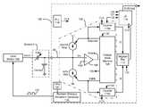
- An embodiment of the touch surface controller 100 disclosed hereinemploys improved detection circuitry 150 which, by virtue of its largely digital nature, is easier and simpler to implement. Such circuitry is shown in FIG. 4 .
- the touch surface controller 100preferably both stimulates the pixels in the touch screen 4 , and also detects the capacitance of those pixels in response to that stimulus.
- a representation of the detected capacitance, Xis output to a microprocessor in a computer system (not shown) which amongst other functions interprets the capacitance values from the array of pixels to determine where a touch or simultaneous multiple touches have occurred on the screen 4 , as discussed earlier.
- the touch surface controller 100is implemented as an ASIC. However, this is not strictly necessary as the functionality of the controller 100 can be implemented in many different manners as one skilled in the art will appreciate.
- the controller 100contains a waveform generator 120 for producing a square waveform 122 for stimulating the pixels in the screen 4 .
- This waveform 122is in turn preferably sent to a level shifter 102 to adjust the DC level of the waveform 122 from a level appropriate for the controller 100 (e.g., 3 V) to a value suitable for stimulating the pixels in the screen 4 (e.g., to 18V).
- This shifted waveform, Vstimis shown in the waveforms of FIG. 5 .
- the rising and falling edges of the stimulus waveform, Vstimare intentionally randomized, as shown by the arrows in FIG. 5 .
- Thisis a noise reduction strategy, which randomizes the frequency content of the stimulus waveforms so as to mask the effect of any interfering frequencies that might be present due to externally-injected noise.
- the periods of each cycle of the waveformare varied in a quasi-random fashion using a First-In-First-Out (FIFO) look up table 121 associated with the waveform generator 120 that contains the time interval data for each integration cycle (i.e., from time t 0 to t 1 , from t 1 to t 2 , etc.).
- FIFOFirst-In-First-Out
- a primary aspect of this disclosurerelates to simplified methodologies for detecting the capacitance (Csig) of the pixels in the screen 4 .
- this capacitancecan be varied by a touch, and thus detecting and quantifying this capacitance informs the computer system of the location of the touch.
- the approach enabled by the detection circuitry 150 of FIG. 4quickly produces a digital representation of the pixel capacitance, Csig, without the need for analog signal conditioning by means of amplification, mixing, and offset subtraction and thus yields an inexpensive and simpler design for controller 100 , as the signal conditioning functions can essentially performed in the digital rather than the analog domain.
- the stimulus signal, Vstimis applied to a pixel in the screen ( 4 ).
- This divided voltage, Vinis input into a comparator 106 , whose inverting terminal is connected to a reference voltage, Vref
- Vinnominally be set to a value that is slightly greater than Vref, i.e., Vref+ ⁇ Vin, which as noted above provides a comparator 106 output, Vcomp, of ‘1.’
- Vcompis input to a charge state machine 108 .
- the primary function of the state machine 108is to enable and disable the current source 104 a and the current sink 104 b , as explained below.
- the time during which current source and/or sink 104 a or b is enabledultimately comprises a digital measurement of the capacitance of interest, Csig. However, before explaining why this is so and how this is accomplished, the basic operation of the detection circuitry is first discussed.
- Equation (1)the effect of reducing the charge of Cstray at node Vin is to gradually reduce its voltage from Vref+ ⁇ Vin to approximately Vref.
- the voltageis made to change from time t 0 to time t 0 ′ by the amount of ⁇ Vin.
- Equation (2)is substituted into Equation (3), and solved for ⁇ T the following equation results:
- ⁇ ⁇ ⁇ T⁇ ⁇ ⁇ Vstim * ( Cstray * Csig ) / [ ( Cstray + Csig ) * Isink ] ( Eq . ⁇ 4 )
- Equation (4)From Equation (4), it can be seen that ⁇ T varies with Csig, the only other variable in Equation (4). As a result, ⁇ T, i.e., the time the current sink 104 ( b ) must be enabled to degrade the input voltage by ⁇ Vin, provides a measure of Csig.
- ⁇ Tis measured digitally, thus amounting to a measure for Csig which is also digital in nature.
- a digital measurement of ⁇ T in a preferred embodimentuses the internal clock of the controller, CLK, which is generated by a phased lock loop (PPL) 116 .
- the PLL 16is otherwise used to clock the central microcontroller 114 of the controller 100 .
- the CLK signalhas a significantly smaller period than does the expected duration of ⁇ T and/or the duration of a particular integration cycle, and can for example be 100 times smaller for example. Because of this, the CLK signal can be used to measure ⁇ T with a precise resolution. As shown in FIG.
- the CLK signalis sent to a counter 110 b , which counts a number of cycles, N, of the clock while the current sink enable signal, Esink, is active. Once Esink is disabled, the counter 110 b stops counting and outputs this number of cycles N to a register file 112 where it is stored.
- measurement of the signal of interest, Csigis effectuated by counting the number of clock cycles N needed to deplete the excessive charge ⁇ Vin from the input to the comparator 106 .
- this measurement Nis digital, and that no analog processing (such as demodulation) is necessary to arrive at a result of Csig.
- the disclosed detection circuitryis thus much simpler and cost-effective to implement.
- Csigcan also be measured using the disclosed technique when the stimulation pulse Vstim is not active, i.e., during a next integration cycle between t 1 and t 2 in FIG. 5 .
- Vstimgoes to zero volts, which causes Vin to be reduced below Vref by a given amount, ⁇ Vin.
- the detection circuitry 150operates basically as before, but instead with the goal of increasing the voltage at Vin to Vref.
- the number of measurements of N and N′ taken for each pixelwill generally occur over a much shorter time interval than any relevant touch (e.g., finger) events. Accordingly, it is logical to average these measurements in the controller 110 before exportation the computer system's microprocessor (not shown) for further interpretation.
- the internal microcontroller 114 in the controller 100can receive both N and N′ and average the two to arrive at digital signal X to be exported to the system microprocessor which digitally indicates the signal of interested, Csig; or X can comprise the average of more than one integration cycle (e.g., N 1 , N 1 ′, N 2 , and N 2 ′, etc.); or the average of a certain numbers of N (from counter 110 b ) or N′ (from counter 110 a ).
- the exported values Xcan also comprise the individual measurements.
- the disclose touch surface controller 100provides other benefits that may not be immediately recognizable, but which are explained below.
- the systemis capable of providing a measurement N that is linearly proportional to the signal capacitance, Csig.
- dN/dCsigequals a constant. This is beneficial because it provides an unvarying resolution independent of the magnitude of Csig, which might otherwise vary between touch panel designs or production runs.
- the following equationcorrelates the change in the measurement, dN, to a change in signal capacitance, dCsig:
- dN2 * Nint * fclk * Vstim * dCsig / ( Ics * ( ( Csig ⁇ ⁇ 2 / Cstray ⁇ ⁇ 2 ) + Csig * dCsig / Cstray 2 + 1 ) ) ( Eq . ⁇ 5 ) where, the number ‘2’ accounts for charge and discharge cycle per integration cycle; Nint is the number of integration cycles, fclk is the frequency of the clock, CLK; Ics is the sink or source current; dCsig is the change in signal capacitance; and Cstray is the static stray capacitance of the column electrode.
- the equationshows that the change in readings, dN, is in good approximation linearly proportional to the change in signal capacitance, dCsig.
- Equation (7)shows that the static stray capacitance, Cstray, essentially drops out of the equation, such that the count, dN, is purely a function of the signal capacitance, Csig.
- the analog implementation of the '313 applicationis also capable of rejecting stray capacitance by keeping the input node at virtual ground, effectively maintaining the voltage across the stray capacitance and thus effectively eliminating the stray capacitance because its net-charge is zero.
- offset compensation for the digital controller 100is still necessary.
- Most of the signal ⁇ Vinis static, and there is only a small change of ⁇ Vin due to the modulation of Csig by dCsig.
- the offset compensationis easily addressed in the digital controller 100 either by dedicated offset circuitry operating in the digital domain or by the microcontroller. In either case, the digital offset compensation is much simpler to implement than the analog offset compensation illustrated above with respect to the '313 application.
- the improved design for the controller 100is capable of rejecting any dynamic stray capacitance, dCstray.
- Dynamic stray capacitancecan result on a given column when the user touches a pixel lying along that column.
- the added stray capacitance on that columnaffects all pixels along that column, such that all pixels on the column may erroneously be interpreted as the location of a touch. It is accordingly important to limit the effect of the dynamic stray capacitance.
- Cstrayis approximately equal to 18 pF
- Csigis approximately equal to 0.7 pF
- dCstray(assuming for sake of argument that it is relatively large) might be equal to a value as high as 20 pF.
- dNas computed from Equation (8) would be 2.1%. Because it is typically permissible for dN to be ⁇ 15%, a 2.1% change in N for corresponding changes in Cstray is permissible, and essentially negligible. In short, these numbers justify the ability of the disclosed technique to reject dynamic stray capacitance.
- the total number of integration cycles Nint and thus integration timeis programmable via the microcontroller 114 and determines the resolution of the measurement, N. Prolonging the integration time yields higher resolution of the dCsig measurement and also reduces the effect of induced noise, at the expense of spending more time for each measurement.
- the microcontroller 114initiates a measurement by first resetting the counters 110 a and 110 b via signal 132 then enabling the charge state machine 108 via control signal 130 . After a programmable integration period set by programmable parameter Nint, the microcontroller 114 loads the count values N and N′ into register file 112 via load signal 131 .
- the controller 100may have registers that allow setting the voltage reference level for the comparator 106 and for setting the sink and source current for current sources 104 a and 104 b via microcontroller 114 .
- either the microcontroller 114 and/or other dedicated logicmay randomize or vary the sink and/or source currents and/or reference voltage Vref during an integration interval to reduce the systems susceptibility to externally introduced noise.
- the detection circuitry 150actually comprises a channel which handles one column 82 of the screen 4 .
- the detection circuitry 150actually comprises a channel which handles one column 82 of the screen 4 .
- the charge state machine 108 of each channelprovides a hold signal 135 to indicate whether a charge/discharge cycle is in progress. Assuming that the hold signal 135 is active high, and that the hold signals from each channel are logically ORed together (not shown), the resulting signal, when low, indicates to the microcontroller 114 that all the channels have completed their respective charge/discharge cycles. At that point, the microcontroller 114 can signal the waveform generator 120 to retrieve the next random stimulus value(s) from FIFO 121 and to output an appropriate stimulus waveform.
Landscapes
- Engineering & Computer Science (AREA)
- General Engineering & Computer Science (AREA)
- Theoretical Computer Science (AREA)
- Human Computer Interaction (AREA)
- Physics & Mathematics (AREA)
- General Physics & Mathematics (AREA)
- Position Input By Displaying (AREA)
Abstract
Description
Vin=[Csig/(Csig+Cstray)]*Vstim (Eq. 1)
This divided voltage, Vin, is input into a
ΔVin=[Csig/(Csig+Cstray)]*ΔVstim (Eq. 2)
Moreover, from the well-known equation I=C dV/dt, it is observed that:
Isink=Cstray*(ΔVin/ΔT) (Eq. 3)
When Equation (2) is substituted into Equation (3), and solved for ΔT the following equation results:
where, the number ‘2’ accounts for charge and discharge cycle per integration cycle; Nint is the number of integration cycles, fclk is the frequency of the clock, CLK; Ics is the sink or source current; dCsig is the change in signal capacitance; and Cstray is the static stray capacitance of the column electrode.
dN=2×Nint*fclk*Vstm*dCsig/Ics (Eq. 6)
or
dN/dCSIG=2×Nint*fclk*Vstm/Ics (Eq. 7)
The equation shows that the change in readings, dN, is in good approximation linearly proportional to the change in signal capacitance, dCsig.
dN=100*(1−[Cs3/(Cs3+Csig2*dCstray)]) (Eq. 8)
where Cs3=Cstray*CSig2+Cstray2*Csig+Csig*Cstray*dCstray. Since Csig is much smaller that Cstray, Cs3is much greater that Csig2*dCstray, and hence Equation (8) can be simplified to:
dN˜100*(1−[Cs3/Cs3])˜0 (Eq. 9)
In short, the count N is essentially independent of changes to Cstray, i.e., dCstray.
Claims (33)
ΔT=ΔVstim*(Cstray*Csig)/[(Cstray+Csig)*Isink]
Priority Applications (3)
| Application Number | Priority Date | Filing Date | Title |
|---|---|---|---|
| US11/621,067US8054299B2 (en) | 2007-01-08 | 2007-01-08 | Digital controller for a true multi-point touch surface useable in a computer system |
| PCT/US2008/050442WO2008086315A2 (en) | 2007-01-08 | 2008-01-07 | Digital controller for a true multi-point surface useable in a computer system |
| TW097100721ATWI405111B (en) | 2007-01-08 | 2008-01-08 | Digital controller for a true multi-point touch surface useable in a computer system |
Applications Claiming Priority (1)
| Application Number | Priority Date | Filing Date | Title |
|---|---|---|---|
| US11/621,067US8054299B2 (en) | 2007-01-08 | 2007-01-08 | Digital controller for a true multi-point touch surface useable in a computer system |
Publications (2)
| Publication Number | Publication Date |
|---|---|
| US20080165134A1 US20080165134A1 (en) | 2008-07-10 |
| US8054299B2true US8054299B2 (en) | 2011-11-08 |
Family
ID=39593848
Family Applications (1)
| Application Number | Title | Priority Date | Filing Date |
|---|---|---|---|
| US11/621,067Expired - Fee RelatedUS8054299B2 (en) | 2007-01-08 | 2007-01-08 | Digital controller for a true multi-point touch surface useable in a computer system |
Country Status (3)
| Country | Link |
|---|---|
| US (1) | US8054299B2 (en) |
| TW (1) | TWI405111B (en) |
| WO (1) | WO2008086315A2 (en) |
Cited By (15)
| Publication number | Priority date | Publication date | Assignee | Title |
|---|---|---|---|---|
| US20090256822A1 (en)* | 2008-04-15 | 2009-10-15 | Nicholas Amireh | Touch screen remote control device for use with a toy |
| US20100073324A1 (en)* | 2008-09-19 | 2010-03-25 | Tpo Displays Corp. | Sensing circuit discharge control method and device for touch panel |
| US20110261008A1 (en)* | 2010-04-22 | 2011-10-27 | Maxim Integrated Products, Inc. | Use of random sampling technique to reduce finger-coupled noise |
| US8321174B1 (en) | 2008-09-26 | 2012-11-27 | Cypress Semiconductor Corporation | System and method to measure capacitance of capacitive sensor array |
| US8358142B2 (en) | 2008-02-27 | 2013-01-22 | Cypress Semiconductor Corporation | Methods and circuits for measuring mutual and self capacitance |
| US20130181947A1 (en)* | 2011-12-21 | 2013-07-18 | Samsung Electro-Mechanics Co., Ltd. | Touch screen panel |
| US8525798B2 (en) | 2008-01-28 | 2013-09-03 | Cypress Semiconductor Corporation | Touch sensing |
| US8570052B1 (en) | 2008-02-27 | 2013-10-29 | Cypress Semiconductor Corporation | Methods and circuits for measuring mutual and self capacitance |
| US8593212B2 (en)* | 2012-03-27 | 2013-11-26 | Chunghwa Picture Tubes, Ltd. | Signal noise ratio control system and method thereof |
| US8874396B1 (en)* | 2013-06-28 | 2014-10-28 | Cypress Semiconductor Corporation | Injected touch noise analysis |
| US20150214899A1 (en)* | 2014-01-27 | 2015-07-30 | Pixart Imaging Inc. | Amplifying circuit and touch control sensing system |
| US20150378511A1 (en)* | 2014-06-26 | 2015-12-31 | Sitronix Technology Corp. | Capacitive Voltage Information Sensing Circuit and Related Anti-Noise Touch Circuit |
| US20160034102A1 (en)* | 2013-04-15 | 2016-02-04 | Fogale Nanotech | Method of multi-zone capacitive sensing, device and apparatus implementing the method |
| US9442610B2 (en) | 2010-04-22 | 2016-09-13 | Qualcomm Technologies, Inc. | Noise cancellation technique for capacitive touchscreen controller using differential sensing |
| US10725583B2 (en)* | 2016-06-30 | 2020-07-28 | Synaptics Incorporated | Input device receiver with delta-sigma modulator |
Families Citing this family (44)
| Publication number | Priority date | Publication date | Assignee | Title |
|---|---|---|---|---|
| US8547114B2 (en) | 2006-11-14 | 2013-10-01 | Cypress Semiconductor Corporation | Capacitance to code converter with sigma-delta modulator |
| US8089288B1 (en) | 2006-11-16 | 2012-01-03 | Cypress Semiconductor Corporation | Charge accumulation capacitance sensor with linear transfer characteristic |
| US8054299B2 (en) | 2007-01-08 | 2011-11-08 | Apple Inc. | Digital controller for a true multi-point touch surface useable in a computer system |
| US8570053B1 (en) | 2007-07-03 | 2013-10-29 | Cypress Semiconductor Corporation | Capacitive field sensor with sigma-delta modulator |
| US8169238B1 (en) | 2007-07-03 | 2012-05-01 | Cypress Semiconductor Corporation | Capacitance to frequency converter |
| US7797115B2 (en)* | 2007-08-13 | 2010-09-14 | Nuvoton Technology Corporation | Time interval measurement for capacitive detection |
| EP2187291A4 (en)* | 2007-09-05 | 2012-06-13 | Panasonic Corp | PORTABLE TERMINAL DEVICE AND DISPLAY CONTROL TECHNIQUE |
| US9104273B1 (en)* | 2008-02-29 | 2015-08-11 | Cypress Semiconductor Corporation | Multi-touch sensing method |
| TWI383310B (en)* | 2008-03-14 | 2013-01-21 | Tpo Displays Corp | Control method, circuit, and electronic system utilizing the same |
| US8260565B2 (en)* | 2008-08-22 | 2012-09-04 | Brookhaven Science Associates, Llc | High dynamic range charge measurements |
| WO2010036545A2 (en)* | 2008-09-24 | 2010-04-01 | 3M Innovative Properties Company | Mutual capacitance measuring circuits and methods |
| JP2010140322A (en)* | 2008-12-12 | 2010-06-24 | Sony Corp | Information processing apparatus, information processing method, program, and information processing system |
| TWI376624B (en)* | 2008-12-23 | 2012-11-11 | Integrated Digital Tech Inc | Force-sensing modules for light sensitive screens |
| EP2204726A1 (en) | 2008-12-30 | 2010-07-07 | STMicroelectronics R&D Oy | Touch screen controller |
| JP5185155B2 (en)* | 2009-02-24 | 2013-04-17 | 株式会社ジャパンディスプレイセントラル | Liquid crystal display |
| CN102460357B (en) | 2009-05-29 | 2016-04-27 | 3M创新有限公司 | High-speed multi-touch touch device and its controller |
| CN102447836A (en) | 2009-06-16 | 2012-05-09 | 英特尔公司 | Camera applications in a handheld device |
| KR101658991B1 (en)* | 2009-06-19 | 2016-09-22 | 삼성전자주식회사 | Touch panel and electronic device including the touch panel |
| KR101667801B1 (en) | 2009-06-19 | 2016-10-20 | 삼성전자주식회사 | Touch panel and electronic device including the touch panel |
| US8436822B2 (en)* | 2009-06-24 | 2013-05-07 | Himax Technologies Limited | Touch panel |
| KR101085403B1 (en)* | 2009-07-21 | 2011-11-21 | 주식회사 코아리버 | Method and device for sensing proximity touch |
| TWI447625B (en)* | 2009-09-14 | 2014-08-01 | Au Optronics Corp | Capacitive touch detection system and detection signal receiving and waveform shaping module |
| US9753586B2 (en) | 2009-10-08 | 2017-09-05 | 3M Innovative Properties Company | Multi-touch touch device with multiple drive frequencies and maximum likelihood estimation |
| US8773366B2 (en)* | 2009-11-16 | 2014-07-08 | 3M Innovative Properties Company | Touch sensitive device using threshold voltage signal |
| US8411066B2 (en) | 2010-01-05 | 2013-04-02 | 3M Innovative Properties Company | High speed noise tolerant multi-touch touch device and controller therefor |
| KR101616875B1 (en) | 2010-01-07 | 2016-05-02 | 삼성전자주식회사 | Touch panel and electronic device including the touch panel |
| KR101631892B1 (en) | 2010-01-28 | 2016-06-21 | 삼성전자주식회사 | Touch panel and electronic device including the touch panel |
| KR20110091380A (en)* | 2010-02-05 | 2011-08-11 | 삼성전자주식회사 | Noise compensation method and device of touch panel |
| KR101710523B1 (en) | 2010-03-22 | 2017-02-27 | 삼성전자주식회사 | Touch panel and electronic device including the touch panel |
| KR20110112128A (en)* | 2010-04-06 | 2011-10-12 | 삼성전자주식회사 | Parasitic capacitance compensation method and apparatus of touch panel |
| JP5523191B2 (en)* | 2010-04-30 | 2014-06-18 | 株式会社ジャパンディスプレイ | Display device with touch detection function |
| KR101661728B1 (en) | 2010-05-11 | 2016-10-04 | 삼성전자주식회사 | User's input apparatus and electronic device including the user's input apparatus |
| EP2577434A2 (en) | 2010-05-25 | 2013-04-10 | 3M Innovative Properties Company | High speed low power multi-touch touch device and controller therefor |
| US9389724B2 (en) | 2010-09-09 | 2016-07-12 | 3M Innovative Properties Company | Touch sensitive device with stylus support |
| US10019119B2 (en) | 2010-09-09 | 2018-07-10 | 3M Innovative Properties Company | Touch sensitive device with stylus support |
| US9823785B2 (en) | 2010-09-09 | 2017-11-21 | 3M Innovative Properties Company | Touch sensitive device with stylus support |
| KR101809191B1 (en) | 2010-10-11 | 2018-01-18 | 삼성전자주식회사 | Touch panel |
| KR101735715B1 (en) | 2010-11-23 | 2017-05-15 | 삼성전자주식회사 | Input sensing circuit and touch panel including the input sensing circuit |
| US8743062B2 (en) | 2010-12-03 | 2014-06-03 | Apple Inc. | Noise reduction for touch controller |
| KR101784436B1 (en) | 2011-04-18 | 2017-10-11 | 삼성전자주식회사 | Touch panel and driving device for the touch panel |
| WO2013066993A2 (en)* | 2011-10-31 | 2013-05-10 | Analog Devices, Inc. | Noise compensation techniques for capacitive touch screen systems |
| AT511664B1 (en)* | 2012-10-17 | 2016-01-15 | Avl List Gmbh | Digital charge amplifier |
| US8890841B2 (en) | 2013-03-13 | 2014-11-18 | 3M Innovative Properties Company | Capacitive-based touch apparatus and method therefor, with reduced interference |
| US10061444B2 (en)* | 2013-07-31 | 2018-08-28 | Apple Inc. | Self capacitance touch sensing |
Citations (32)
| Publication number | Priority date | Publication date | Assignee | Title |
|---|---|---|---|---|
| US5483261A (en) | 1992-02-14 | 1996-01-09 | Itu Research, Inc. | Graphical input controller and method with rear screen image detection |
| US5488204A (en) | 1992-06-08 | 1996-01-30 | Synaptics, Incorporated | Paintbrush stylus for capacitive touch sensor pad |
| WO1996018179A1 (en) | 1994-12-07 | 1996-06-13 | Cirque Corporation | Capacitance-based proximity sensors with interference rejection apparatus and methods |
| US5825352A (en) | 1996-01-04 | 1998-10-20 | Logitech, Inc. | Multiple fingers contact sensing method for emulating mouse buttons and mouse operations on a touch sensor pad |
| US5835079A (en) | 1996-06-13 | 1998-11-10 | International Business Machines Corporation | Virtual pointing device for touchscreens |
| US5856822A (en)* | 1995-10-27 | 1999-01-05 | 02 Micro, Inc. | Touch-pad digital computer pointing-device |
| US5880411A (en) | 1992-06-08 | 1999-03-09 | Synaptics, Incorporated | Object position detector with edge motion feature and gesture recognition |
| JP2000163031A (en) | 1998-11-25 | 2000-06-16 | Seiko Epson Corp | Portable information devices and information storage media |
| US6188391B1 (en) | 1998-07-09 | 2001-02-13 | Synaptics, Inc. | Two-layer capacitive touchpad and method of making same |
| US6191723B1 (en)* | 1999-07-22 | 2001-02-20 | Fluke Corporation | Fast capacitance measurement |
| US6275047B1 (en)* | 1999-03-12 | 2001-08-14 | Fluke Corporation | Capacitance measurement |
| US6310610B1 (en) | 1997-12-04 | 2001-10-30 | Nortel Networks Limited | Intelligent touch display |
| US6323846B1 (en) | 1998-01-26 | 2001-11-27 | University Of Delaware | Method and apparatus for integrating manual input |
| JP2002342033A (en) | 2001-05-21 | 2002-11-29 | Sony Corp | Non-contact type user input device |
| US6570557B1 (en) | 2001-02-10 | 2003-05-27 | Finger Works, Inc. | Multi-touch system and method for emulating modifier keys via fingertip chords |
| US6677932B1 (en) | 2001-01-28 | 2004-01-13 | Finger Works, Inc. | System and method for recognizing touch typing under limited tactile feedback conditions |
| US6690387B2 (en) | 2001-12-28 | 2004-02-10 | Koninklijke Philips Electronics N.V. | Touch-screen image scrolling system and method |
| US20040104826A1 (en) | 2002-10-31 | 2004-06-03 | Harald Philipp | Charge transfer capacitive position sensor |
| US6795359B1 (en)* | 2003-06-10 | 2004-09-21 | Micron Technology, Inc. | Methods and apparatus for measuring current as in sensing a memory cell |
| US20040243747A1 (en)* | 2001-05-21 | 2004-12-02 | Junichi Rekimoto | User input apparatus, computer connected to user input apparatus, method of controlling computer connected to user input apparatus, and storage medium |
| US20060026536A1 (en) | 2004-07-30 | 2006-02-02 | Apple Computer, Inc. | Gestures for touch sensitive input devices |
| US20060033724A1 (en) | 2004-07-30 | 2006-02-16 | Apple Computer, Inc. | Virtual input device placement on a touch screen user interface |
| US20060053387A1 (en) | 2004-07-30 | 2006-03-09 | Apple Computer, Inc. | Operation of a computer with touch screen interface |
| US7015894B2 (en) | 2001-09-28 | 2006-03-21 | Ricoh Company, Ltd. | Information input and output system, method, storage medium, and carrier wave |
| US20060085757A1 (en) | 2004-07-30 | 2006-04-20 | Apple Computer, Inc. | Activating virtual keys of a touch-screen virtual keyboard |
| US20060097991A1 (en) | 2004-05-06 | 2006-05-11 | Apple Computer, Inc. | Multipoint touchscreen |
| US20060197753A1 (en) | 2005-03-04 | 2006-09-07 | Hotelling Steven P | Multi-functional hand-held device |
| US7145350B2 (en)* | 2003-07-22 | 2006-12-05 | Vega Grieshaber Kg | Process and a circuit arrangement for evaluating a measuring capacitance |
| US20070229466A1 (en)* | 2006-03-30 | 2007-10-04 | Cypress Semiconductor Corporation | Apparatus and method for recognizing a tap gesture on a touch sensing device |
| US20070257890A1 (en) | 2006-05-02 | 2007-11-08 | Apple Computer, Inc. | Multipoint touch surface controller |
| USRE40153E1 (en) | 2001-02-10 | 2008-03-18 | Apple Inc. | Multi-touch system and method for emulating modifier keys via fingertip chords |
| US20080165134A1 (en) | 2007-01-08 | 2008-07-10 | Apple Computer, Inc. | Digital Controller for a True Multi-point Touch Surface Useable in a Computer System |
Family Cites Families (2)
| Publication number | Priority date | Publication date | Assignee | Title |
|---|---|---|---|---|
| DE19901291C2 (en)* | 1999-01-15 | 2002-04-18 | Sez Semiconduct Equip Zubehoer | Device for the etching treatment of a disc-shaped object |
| TWI291646B (en)* | 2005-05-03 | 2007-12-21 | Asustek Comp Inc | A display card with touch screen controller |
- 2007
- 2007-01-08USUS11/621,067patent/US8054299B2/ennot_activeExpired - Fee Related
- 2008
- 2008-01-07WOPCT/US2008/050442patent/WO2008086315A2/enactiveApplication Filing
- 2008-01-08TWTW097100721Apatent/TWI405111B/ennot_activeIP Right Cessation
Patent Citations (39)
| Publication number | Priority date | Publication date | Assignee | Title |
|---|---|---|---|---|
| US5483261A (en) | 1992-02-14 | 1996-01-09 | Itu Research, Inc. | Graphical input controller and method with rear screen image detection |
| US5880411A (en) | 1992-06-08 | 1999-03-09 | Synaptics, Incorporated | Object position detector with edge motion feature and gesture recognition |
| US5488204A (en) | 1992-06-08 | 1996-01-30 | Synaptics, Incorporated | Paintbrush stylus for capacitive touch sensor pad |
| US5565658A (en)* | 1992-07-13 | 1996-10-15 | Cirque Corporation | Capacitance-based proximity with interference rejection apparatus and methods |
| WO1996018179A1 (en) | 1994-12-07 | 1996-06-13 | Cirque Corporation | Capacitance-based proximity sensors with interference rejection apparatus and methods |
| US5856822A (en)* | 1995-10-27 | 1999-01-05 | 02 Micro, Inc. | Touch-pad digital computer pointing-device |
| US5825352A (en) | 1996-01-04 | 1998-10-20 | Logitech, Inc. | Multiple fingers contact sensing method for emulating mouse buttons and mouse operations on a touch sensor pad |
| US5835079A (en) | 1996-06-13 | 1998-11-10 | International Business Machines Corporation | Virtual pointing device for touchscreens |
| US6310610B1 (en) | 1997-12-04 | 2001-10-30 | Nortel Networks Limited | Intelligent touch display |
| US7339580B2 (en) | 1998-01-26 | 2008-03-04 | Apple Inc. | Method and apparatus for integrating manual input |
| US6888536B2 (en) | 1998-01-26 | 2005-05-03 | The University Of Delaware | Method and apparatus for integrating manual input |
| US6323846B1 (en) | 1998-01-26 | 2001-11-27 | University Of Delaware | Method and apparatus for integrating manual input |
| US6188391B1 (en) | 1998-07-09 | 2001-02-13 | Synaptics, Inc. | Two-layer capacitive touchpad and method of making same |
| JP2000163031A (en) | 1998-11-25 | 2000-06-16 | Seiko Epson Corp | Portable information devices and information storage media |
| US6275047B1 (en)* | 1999-03-12 | 2001-08-14 | Fluke Corporation | Capacitance measurement |
| US6191723B1 (en)* | 1999-07-22 | 2001-02-20 | Fluke Corporation | Fast capacitance measurement |
| US6677932B1 (en) | 2001-01-28 | 2004-01-13 | Finger Works, Inc. | System and method for recognizing touch typing under limited tactile feedback conditions |
| USRE40153E1 (en) | 2001-02-10 | 2008-03-18 | Apple Inc. | Multi-touch system and method for emulating modifier keys via fingertip chords |
| US6570557B1 (en) | 2001-02-10 | 2003-05-27 | Finger Works, Inc. | Multi-touch system and method for emulating modifier keys via fingertip chords |
| JP2002342033A (en) | 2001-05-21 | 2002-11-29 | Sony Corp | Non-contact type user input device |
| US20040243747A1 (en)* | 2001-05-21 | 2004-12-02 | Junichi Rekimoto | User input apparatus, computer connected to user input apparatus, method of controlling computer connected to user input apparatus, and storage medium |
| US7015894B2 (en) | 2001-09-28 | 2006-03-21 | Ricoh Company, Ltd. | Information input and output system, method, storage medium, and carrier wave |
| US7184064B2 (en) | 2001-12-28 | 2007-02-27 | Koninklijke Philips Electronics N.V. | Touch-screen image scrolling system and method |
| US6690387B2 (en) | 2001-12-28 | 2004-02-10 | Koninklijke Philips Electronics N.V. | Touch-screen image scrolling system and method |
| US20040104826A1 (en) | 2002-10-31 | 2004-06-03 | Harald Philipp | Charge transfer capacitive position sensor |
| US6795359B1 (en)* | 2003-06-10 | 2004-09-21 | Micron Technology, Inc. | Methods and apparatus for measuring current as in sensing a memory cell |
| US7145350B2 (en)* | 2003-07-22 | 2006-12-05 | Vega Grieshaber Kg | Process and a circuit arrangement for evaluating a measuring capacitance |
| US20060097991A1 (en) | 2004-05-06 | 2006-05-11 | Apple Computer, Inc. | Multipoint touchscreen |
| US20060026535A1 (en) | 2004-07-30 | 2006-02-02 | Apple Computer Inc. | Mode-based graphical user interfaces for touch sensitive input devices |
| US20060026521A1 (en) | 2004-07-30 | 2006-02-02 | Apple Computer, Inc. | Gestures for touch sensitive input devices |
| US20060033724A1 (en) | 2004-07-30 | 2006-02-16 | Apple Computer, Inc. | Virtual input device placement on a touch screen user interface |
| US20060053387A1 (en) | 2004-07-30 | 2006-03-09 | Apple Computer, Inc. | Operation of a computer with touch screen interface |
| US20060085757A1 (en) | 2004-07-30 | 2006-04-20 | Apple Computer, Inc. | Activating virtual keys of a touch-screen virtual keyboard |
| US20060026536A1 (en) | 2004-07-30 | 2006-02-02 | Apple Computer, Inc. | Gestures for touch sensitive input devices |
| US20060197753A1 (en) | 2005-03-04 | 2006-09-07 | Hotelling Steven P | Multi-functional hand-held device |
| US20070229466A1 (en)* | 2006-03-30 | 2007-10-04 | Cypress Semiconductor Corporation | Apparatus and method for recognizing a tap gesture on a touch sensing device |
| US20070257890A1 (en) | 2006-05-02 | 2007-11-08 | Apple Computer, Inc. | Multipoint touch surface controller |
| US20080165134A1 (en) | 2007-01-08 | 2008-07-10 | Apple Computer, Inc. | Digital Controller for a True Multi-point Touch Surface Useable in a Computer System |
| WO2008086315A2 (en) | 2007-01-08 | 2008-07-17 | Apple Inc. | Digital controller for a true multi-point surface useable in a computer system |
Non-Patent Citations (5)
| Title |
|---|
| International Search Report mailed Jan. 29, 2009, for PCT Application No. PCT/US2008/050442, filed Jan. 7, 2008, five pages. |
| Lee, S.K. et al. (Apr. 1985). "A Multi-Touch Three Dimensional Touch-Sensitive Tablet," Proceedings of CHI: ACM Conference on Human Factors in Computing Systems, pp. 21-25. |
| Rubine, D.H. (Dec. 1991). "The Automatic Recognition of Gestures," CMU-CS-91-202, Submitted in Partial Fulfillment of the Requirements of the Degree of Doctor of Philosophy in Computer Science at Carnegie Mellon University, 285 pages. |
| Rubine, D.H. (May 1992). "Combining Gestures and Direct Manipulation," CHI '92, pp. 659-660. |
| Westerman, W. (Spring 1999). "Hand Tracking, Finger Identification, and Chordic Manipulation on a Multi-Touch Surface," A Dissertation Submitted to the Faculty of the University of Delaware in Partial Fulfillment of the Requirements for the Degree of Doctor of Philosophy in Electrical Engineering, 364 pages. |
Cited By (30)
| Publication number | Priority date | Publication date | Assignee | Title |
|---|---|---|---|---|
| US8525798B2 (en) | 2008-01-28 | 2013-09-03 | Cypress Semiconductor Corporation | Touch sensing |
| US9760192B2 (en) | 2008-01-28 | 2017-09-12 | Cypress Semiconductor Corporation | Touch sensing |
| US9494628B1 (en) | 2008-02-27 | 2016-11-15 | Parade Technologies, Ltd. | Methods and circuits for measuring mutual and self capacitance |
| US8570052B1 (en) | 2008-02-27 | 2013-10-29 | Cypress Semiconductor Corporation | Methods and circuits for measuring mutual and self capacitance |
| US9423427B2 (en) | 2008-02-27 | 2016-08-23 | Parade Technologies, Ltd. | Methods and circuits for measuring mutual and self capacitance |
| US8358142B2 (en) | 2008-02-27 | 2013-01-22 | Cypress Semiconductor Corporation | Methods and circuits for measuring mutual and self capacitance |
| US8692563B1 (en) | 2008-02-27 | 2014-04-08 | Cypress Semiconductor Corporation | Methods and circuits for measuring mutual and self capacitance |
| US20090256822A1 (en)* | 2008-04-15 | 2009-10-15 | Nicholas Amireh | Touch screen remote control device for use with a toy |
| US8564547B2 (en)* | 2008-04-15 | 2013-10-22 | Mattel, Inc. | Touch screen remote control device for use with a toy |
| US20100073324A1 (en)* | 2008-09-19 | 2010-03-25 | Tpo Displays Corp. | Sensing circuit discharge control method and device for touch panel |
| US8194050B2 (en)* | 2008-09-19 | 2012-06-05 | Chimei Innolux Corporation | Sensing circuit discharge control method and device for touch panel |
| US11029795B2 (en) | 2008-09-26 | 2021-06-08 | Cypress Semiconductor Corporation | System and method to measure capacitance of capacitive sensor array |
| US8321174B1 (en) | 2008-09-26 | 2012-11-27 | Cypress Semiconductor Corporation | System and method to measure capacitance of capacitive sensor array |
| US10386969B1 (en) | 2008-09-26 | 2019-08-20 | Cypress Semiconductor Corporation | System and method to measure capacitance of capacitive sensor array |
| US20110261008A1 (en)* | 2010-04-22 | 2011-10-27 | Maxim Integrated Products, Inc. | Use of random sampling technique to reduce finger-coupled noise |
| US9870097B2 (en) | 2010-04-22 | 2018-01-16 | Qualcomm Incorporated | Noise cancellation technique for capacitive touchscreen controller using differential sensing |
| US9391607B2 (en)* | 2010-04-22 | 2016-07-12 | Qualcomm Technologies, Inc. | Use of random sampling technique to reduce finger-coupled noise |
| US9442610B2 (en) | 2010-04-22 | 2016-09-13 | Qualcomm Technologies, Inc. | Noise cancellation technique for capacitive touchscreen controller using differential sensing |
| US20130181947A1 (en)* | 2011-12-21 | 2013-07-18 | Samsung Electro-Mechanics Co., Ltd. | Touch screen panel |
| US8593212B2 (en)* | 2012-03-27 | 2013-11-26 | Chunghwa Picture Tubes, Ltd. | Signal noise ratio control system and method thereof |
| US10592046B2 (en)* | 2013-04-15 | 2020-03-17 | Quickstep Technologies Llc | Method of multi-zone capacitive sensing, device and apparatus implementing the method |
| US20160034102A1 (en)* | 2013-04-15 | 2016-02-04 | Fogale Nanotech | Method of multi-zone capacitive sensing, device and apparatus implementing the method |
| US20150199046A1 (en)* | 2013-06-28 | 2015-07-16 | Cypress Semiconductor Corporation | Injected Touch Noise Analysis |
| US9547399B2 (en)* | 2013-06-28 | 2017-01-17 | Parade Technologies, Ltd. | Injected touch noise analysis |
| US8874396B1 (en)* | 2013-06-28 | 2014-10-28 | Cypress Semiconductor Corporation | Injected touch noise analysis |
| US9197167B2 (en)* | 2014-01-27 | 2015-11-24 | Pixart Imaging Inc. | Amplifying circuit and touch control sensing system |
| US20150214899A1 (en)* | 2014-01-27 | 2015-07-30 | Pixart Imaging Inc. | Amplifying circuit and touch control sensing system |
| US9524056B2 (en)* | 2014-06-26 | 2016-12-20 | Sitronix Technology Corp. | Capacitive voltage information sensing circuit and related anti-noise touch circuit |
| US20150378511A1 (en)* | 2014-06-26 | 2015-12-31 | Sitronix Technology Corp. | Capacitive Voltage Information Sensing Circuit and Related Anti-Noise Touch Circuit |
| US10725583B2 (en)* | 2016-06-30 | 2020-07-28 | Synaptics Incorporated | Input device receiver with delta-sigma modulator |
Also Published As
| Publication number | Publication date |
|---|---|
| US20080165134A1 (en) | 2008-07-10 |
| TWI405111B (en) | 2013-08-11 |
| WO2008086315A3 (en) | 2009-03-19 |
| TW200842682A (en) | 2008-11-01 |
| WO2008086315A2 (en) | 2008-07-17 |
Similar Documents
| Publication | Publication Date | Title |
|---|---|---|
| US8054299B2 (en) | Digital controller for a true multi-point touch surface useable in a computer system | |
| US11592948B2 (en) | Channel scan logic | |
| CN101479692B (en) | multi-touch surface controller | |
| US9965100B2 (en) | Scan sequence generator | |
| US9389724B2 (en) | Touch sensitive device with stylus support | |
| US8411066B2 (en) | High speed noise tolerant multi-touch touch device and controller therefor | |
| US9823785B2 (en) | Touch sensitive device with stylus support | |
| US10019119B2 (en) | Touch sensitive device with stylus support | |
| US9417739B2 (en) | High speed multi-touch touch device and controller therefor | |
| HK1135487B (en) | Multipoint touch surface controller |
Legal Events
| Date | Code | Title | Description |
|---|---|---|---|
| AS | Assignment | Owner name:APPLE COMPUTER, INC., CALIFORNIA Free format text:ASSIGNMENT OF ASSIGNORS INTEREST;ASSIGNOR:KRAH, CHRISTOPH H.;REEL/FRAME:018725/0271 Effective date:20070108 | |
| AS | Assignment | Owner name:APPLE INC., CALIFORNIA Free format text:CHANGE OF NAME;ASSIGNOR:APPLE COMPUTER, INC.;REEL/FRAME:019265/0961 Effective date:20070109 Owner name:APPLE INC.,CALIFORNIA Free format text:CHANGE OF NAME;ASSIGNOR:APPLE COMPUTER, INC.;REEL/FRAME:019265/0961 Effective date:20070109 | |
| FEPP | Fee payment procedure | Free format text:PAYOR NUMBER ASSIGNED (ORIGINAL EVENT CODE: ASPN); ENTITY STATUS OF PATENT OWNER: LARGE ENTITY | |
| STCF | Information on status: patent grant | Free format text:PATENTED CASE | |
| FPAY | Fee payment | Year of fee payment:4 | |
| FEPP | Fee payment procedure | Free format text:MAINTENANCE FEE REMINDER MAILED (ORIGINAL EVENT CODE: REM.); ENTITY STATUS OF PATENT OWNER: LARGE ENTITY | |
| LAPS | Lapse for failure to pay maintenance fees | Free format text:PATENT EXPIRED FOR FAILURE TO PAY MAINTENANCE FEES (ORIGINAL EVENT CODE: EXP.); ENTITY STATUS OF PATENT OWNER: LARGE ENTITY | |
| STCH | Information on status: patent discontinuation | Free format text:PATENT EXPIRED DUE TO NONPAYMENT OF MAINTENANCE FEES UNDER 37 CFR 1.362 | |
| FP | Lapsed due to failure to pay maintenance fee | Effective date:20191108 |