US8054090B2 - Noise handling in capacitive touch sensors - Google Patents
Noise handling in capacitive touch sensorsDownload PDFInfo
- Publication number
- US8054090B2 US8054090B2US12/255,998US25599808AUS8054090B2US 8054090 B2US8054090 B2US 8054090B2US 25599808 AUS25599808 AUS 25599808AUS 8054090 B2US8054090 B2US 8054090B2
- Authority
- US
- United States
- Prior art keywords
- charge
- capacitor
- plate
- measurement
- amount
- Prior art date
- Legal status (The legal status is an assumption and is not a legal conclusion. Google has not performed a legal analysis and makes no representation as to the accuracy of the status listed.)
- Active, expires
Links
Images


Classifications
- G—PHYSICS
- G06—COMPUTING OR CALCULATING; COUNTING
- G06F—ELECTRIC DIGITAL DATA PROCESSING
- G06F3/00—Input arrangements for transferring data to be processed into a form capable of being handled by the computer; Output arrangements for transferring data from processing unit to output unit, e.g. interface arrangements
- G06F3/01—Input arrangements or combined input and output arrangements for interaction between user and computer
- G06F3/03—Arrangements for converting the position or the displacement of a member into a coded form
- G06F3/041—Digitisers, e.g. for touch screens or touch pads, characterised by the transducing means
- G06F3/044—Digitisers, e.g. for touch screens or touch pads, characterised by the transducing means by capacitive means
- G06F3/0446—Digitisers, e.g. for touch screens or touch pads, characterised by the transducing means by capacitive means using a grid-like structure of electrodes in at least two directions, e.g. using row and column electrodes
- G—PHYSICS
- G01—MEASURING; TESTING
- G01R—MEASURING ELECTRIC VARIABLES; MEASURING MAGNETIC VARIABLES
- G01R27/00—Arrangements for measuring resistance, reactance, impedance, or electric characteristics derived therefrom
- G01R27/02—Measuring real or complex resistance, reactance, impedance, or other two-pole characteristics derived therefrom, e.g. time constant
- G01R27/26—Measuring inductance or capacitance; Measuring quality factor, e.g. by using the resonance method; Measuring loss factor; Measuring dielectric constants ; Measuring impedance or related variables
- G01R27/2605—Measuring capacitance
- G—PHYSICS
- G01—MEASURING; TESTING
- G01R—MEASURING ELECTRIC VARIABLES; MEASURING MAGNETIC VARIABLES
- G01R29/00—Arrangements for measuring or indicating electric quantities not covered by groups G01R19/00 - G01R27/00
- G01R29/26—Measuring noise figure; Measuring signal-to-noise ratio
- G—PHYSICS
- G06—COMPUTING OR CALCULATING; COUNTING
- G06F—ELECTRIC DIGITAL DATA PROCESSING
- G06F3/00—Input arrangements for transferring data to be processed into a form capable of being handled by the computer; Output arrangements for transferring data from processing unit to output unit, e.g. interface arrangements
- G06F3/01—Input arrangements or combined input and output arrangements for interaction between user and computer
- G06F3/03—Arrangements for converting the position or the displacement of a member into a coded form
- G06F3/041—Digitisers, e.g. for touch screens or touch pads, characterised by the transducing means
- G06F3/0416—Control or interface arrangements specially adapted for digitisers
- G06F3/0418—Control or interface arrangements specially adapted for digitisers for error correction or compensation, e.g. based on parallax, calibration or alignment
- G06F3/04184—Synchronisation with the driving of the display or the backlighting unit to avoid interferences generated internally
- G—PHYSICS
- G06—COMPUTING OR CALCULATING; COUNTING
- G06F—ELECTRIC DIGITAL DATA PROCESSING
- G06F3/00—Input arrangements for transferring data to be processed into a form capable of being handled by the computer; Output arrangements for transferring data from processing unit to output unit, e.g. interface arrangements
- G06F3/01—Input arrangements or combined input and output arrangements for interaction between user and computer
- G06F3/03—Arrangements for converting the position or the displacement of a member into a coded form
- G06F3/041—Digitisers, e.g. for touch screens or touch pads, characterised by the transducing means
- G06F3/044—Digitisers, e.g. for touch screens or touch pads, characterised by the transducing means by capacitive means
- G06F3/0443—Digitisers, e.g. for touch screens or touch pads, characterised by the transducing means by capacitive means using a single layer of sensing electrodes
Definitions
- the present inventionrelates to noise handling in a capacitive touch sensor for detecting proximity of a body, more especially to a capacitive sensor of the so-called active type which is based on measuring the capacitive coupling between a drive and a sense electrode.
- touch sensitive controlswhich use a capacitive sensor to sense the presence of a body such as a user's finger.
- a form of touch sensitive controlis disclosed in WO-00/44018.
- a pair of electrodesare provided which act as a key so that the presence of a body such as a user's finger is detected as a result of a change in an amount of charge which is transferred between the two electrodes.
- one of the electrodes(labeled X) is driven with a drive circuit and the other of the pair of electrodes (labeled Y) is connected to a charge measurement circuit which detects an amount of charge present on the Y plate when driven by the X plate.
- WO-00/44018several pairs of electrodes can be arranged to form a matrix of sensing areas which can provide an efficient implementation of a touch sensitive two-dimensional position sensor.
- Such two dimensional capacitive transducing (2DCT) sensorsare typically used with devices which include touch sensitive screens or touch sensitive keyboards/keypads which are used in for example in consumer electronic devices and domestic appliances.
- 2DCT sensorshave become increasingly popular and common not only in conjunction with personal computers but also in all manner of other appliances such as personal digital assistants (PDAs), point of sale (POS) terminals, electronic information and ticketing kiosks, kitchen appliances and the like.
- PDAspersonal digital assistants
- POSpoint of sale
- 2DCT sensorsare frequently preferred to mechanical switches for a number of reasons.
- 2DCT sensorsrequire no moving parts and so are less prone to wear than their mechanical counterparts.
- 2DCT sensorscan also be made in relatively small sizes so that correspondingly small, and tightly packed keypad arrays can be provided.
- 2DCT sensorscan be provided beneath an environmentally sealed outer surface/cover panel. This makes their use in wet environments or where there is a danger of dirt or fluids entering a device being controlled attractive.
- manufacturesoften prefer to employ interfaces based on 2DCT sensors in their products because such interfaces are often considered by consumers to be more aesthetically pleasing than conventional mechanical input mechanisms (e.g. push-buttons).
- 2DCT sensorsinclude pen-input tablets and encoders used in machinery for feedback control purposes, for example 2DCT sensors are capable of reporting at least a 2-dimensional coordinate, Cartesian or otherwise, related to the location of an object or human body part by means of a capacitance sensing mechanism.
- touch sensitive capacitive sensorssuch as those described above and disclosed in the above-mentioned disclosures have been successfully deployed in many applications, some applications can present a challenging environment for detecting a change in charge as a result of the presence of a body.
- a touch sensor on a mobile phonecan create a technical problem because there is a variety of disturbing noise signals produced by radio frequency radiation by radio frequency signals and by modulators within the mobile phone.
- a liquid crystal displayLCD
- LCDliquid crystal display
- Other types of displaymay have their own forms of characteristic impulsive noise related to pixel scanning and refresh.
- Sinusoidal noisesuch as that produced by mains electricity may also be present, which can affect the amount of charge detected on a key. This may be significant, for example, when a hand held device such as a mobile telephone is being charged through the mains.
- FIG. 7 of the accompanying drawingsshows an example of sinusoidal noise in the form of a plot of signal strength or amplitude which may be voltage or charge measured with respect to time.
- Various points 220are shown to indicate points at which burst measurements are taken for a touch sensor such as those described above.
- sinusoidal noiserepresented by a line 222
- an amount of charge transferred from a key by a measurement capacitor of the measurement circuitsuch as those described above will vary and therefore could in some circumstances cause a false measurement of the presence of a body.
- FIG. 8 of the accompanying drawingsshows another form of noise, namely rectangular or impulsive noise, i.e. noise having high frequency components, such as that which might be produced by switching the pixels in a LCD display with which the touch panel is integrated.
- a plot of signal strength with respect to timeis shown with sampling points 220 , which might be produced by bursts of measurement cycles in a measurement circuit such as those described above.
- Noise impulses 222are also shown. If a measurement cycle coincides with a rising edge of a noise impulse, as may arise from an LCD switching event, then an erroneous measurement can be produced which can again cause a touch sensor to erroneously detect the presence of a body.
- FIG. 9 of the accompanying drawingsillustrates this situation showing simultaneous sinusoidal and rectangular noise.
- both sinusoidal noise and rectangular noisemay be present during a given time period.
- the amount of noise as well as its frequency componentswill often vary over time.
- Prior art capacitive sensorsadopt a variety of signal processing techniques to filter noise from the acquired signals.
- boxcar averagers and detection integratorshave been used in the past.
- other types of standard filteringcould be used, and may have been used, such as slew rate filters, high frequency pass filters, low frequency pass filters and band pass filters.
- the inventionprovides a method of measuring proximity of a body to a capacitive sensor device comprising a coupling capacitor having a capacitance sensitive to proximity of a body, and a charge accumulation capacitor having first and second plates, the first plate being connected to the coupling capacitor, and the second plate being connected to a voltage output line.
- a signal measurementis made conventionally by transferring charge indicative of the capacitance of the coupling capacitor from the coupling capacitor to the charge accumulation capacitor, and by reading the voltage on the voltage output line, thereby to measure proximity of a body.
- An additional noise measurementis made, either before or after the signal measurement, by emulating or mimicking the signal measurement, but inhibiting charge from arising on the coupling capacitor as a result of proximity of a body, thereby to transfer charge indicative of noise induced on the coupling capacitor to the charge accumulation capacitor, and by reading the voltage on the voltage output line, thereby to measure noise.
- a method of measuring proximity of a body to a capacitive sensor devicecomprising X and Y electrodes forming respective X and Y plates of a coupling capacitor having a capacitance sensitive to proximity of a body, and a charge accumulation capacitor having first and second plates, the first plate being connected to the Y plate of the coupling capacitor, and the second plate being connected to a voltage output line
- the methodcomprising: making a signal measurement by applying one or more cycles of driving the X electrode with an input voltage, thereby to transfer one or more packets of charge indicative of the capacitance of the coupling capacitor from the coupling capacitor to the charge accumulation capacitor, and by reading the voltage on the voltage output line, thereby to measure proximity of a body; and making a noise measurement, either before or after the signal measurement, by emulating or mimicking the signal measurement, but without driving the X electrode, thereby to transfer one or more packets of charge indicative of noise induced on the coupling capacitor to the charge accumulation capacitor,
- a noise measurementcan therefore be obtained whenever desired, for example after every ‘n’ signal measurements, wherein the noise measurement is taken directly from the coupling capacitors that form the sensing nodes of the capacitive sensor device.
- the noise measurementsshould therefore be representative of noise levels when the signal measurements are made, since they are obtained using the same circuit elements and interconnects. Moreover, the noise measurements can be made without any additional hardware requirement on the sensor device.
- the second plate of the charge accumulation capacitoris preferably connected to a pre-charge line operable to inject a predetermined amount of charge onto the second plate
- the second plate of the charge accumulation capacitoris then charged before mimicking the signal measurement, thereby to measure noise through its modulation of the amount of charge initially placed on the charge accumulation capacitor.
- the pre-chargemakes the amount of charge accumulated on the charge accumulation capacitor independent of the sign of the charge induced on the Y plate of the coupling capacitor at each cycle of the noise measurement process. This is useful if the controller is not capable of measuring arbitrary voltages from the charge accumulation capacitor.
- the second plate of the charge accumulation capacitorcan be pre-charged, e.g. to a certain negative or positive voltage, to ensure that noise contributions will not cause the voltage to change sign before read out, but rather only modulate the pre-charge voltage without changing its sign.
- chargemay be transferred to the charge accumulation capacitor in a plurality of cycles, and the voltage on the voltage output line is read after a predetermined number of said cycles.
- the number of cyclesis preferably 1, or a small integer number such as 2, 3, 4 or 5.
- chargemay be transferred to the charge accumulation capacitor in a plurality of cycles, and the voltage on the voltage output line is read after a predetermined number of said cycles.
- chargemay be transferred to the charge accumulation capacitor in a plurality of cycles, wherein the cycles are repeated until the voltage on the voltage output line reaches a threshold value, the number of cycles required to reach the threshold value being read as the measure of the capacitance.
- the number of predetermined cyclescould be 1, but is preferably a higher number so that the charge accumulation capacitor has an averaging effect on any noise.
- the number of cyclesis preferably at least 5, 10, 20, 30, 40, 50 or 100.
- the number of cycles over which charge is transferred from the coupling capacitor to the charge accumulation capacitoris often referred to in the art as the burst length.
- the noise measurementwill typically use short fixed burst lengths, e.g. of only cycle or a few cycles, whereas the signal measurement will typically use longer burst lengths, which may be fixed, i.e. predetermined in number, or variable, i.e. the number required for the signal to reach a threshold value. Consequently the burst length for the noise measurement will typically be shorter than the burst length for the signal measurement.
- the methodis applied by interspersing signal measurements and noise measurements.
- a plurality of signal measurementsare made for each noise measurement.
- the noise measurementsmay be limited so that they only occupy a certain minority of the total measurement time, for example a noise measurement may be made after ‘n’ signal measurements, where n might be at least 2, 3, 4, 5, 10, 20, 50 or 100.
- a noise measurementmight be made once per frame or once every ‘n’ frames, where collection of a frame of touch data is defined as reading a signal measurement from each of the sensing nodes, i.e. each of the coupling capacitors, of the two-dimensional touch panel.
- the inventionalso provides a capacitive sensor device comprising a coupling capacitor having a capacitance sensitive to proximity of a body, and a charge accumulation capacitor having first and second plates, the first plate being connected to the coupling capacitor, and the second plate being connected to a voltage output line, the device being operable in a first mode to make a signal measurement by transferring charge indicative of the capacitance of the coupling capacitor from the coupling capacitor to the charge accumulation capacitor, wherein the voltage on the voltage output line is a measure of proximity of a body; and the device being operable in a second mode to make a noise measurement by mimicking the signal measurement, but without enabling charge to arise on the coupling capacitor through proximity of a body, thereby to transfer charge indicative of noise induced on the coupling capacitor to the charge accumulation capacitor, wherein the voltage on the voltage output line is a measure of noise.
- the inventionfurther provides a capacitive sensor device comprising X and Y electrodes forming respective X and Y plates of a coupling capacitor having a capacitance sensitive to proximity of a body, and a charge accumulation capacitor having first and second plates, the first plate being connected to the Y plate of the coupling capacitor, and the second plate being connected to a voltage output line, the device being operable in a first mode to make a signal measurement by applying successive cycles of driving the X electrode with an input voltage, thereby to transfer successive packets of charge indicative of the capacitance of the coupling capacitor from the coupling capacitor to the charge accumulation capacitor, wherein the voltage on the voltage output line is a measure of proximity of a body; and the device being operable in a second mode to make a noise measurement by mimicking the signal measurement, but without driving the X electrode, thereby to transfer successive packets of charge indicative of noise induced on the coupling capacitor to the charge accumulation capacitor, wherein the voltage on the voltage output line is a measure of noise.
- the second plate of the charge accumulation capacitoris preferably connected to a pre-charge line operable to inject a predetermined amount of charge onto the second plate, and wherein, in the noise measurement mode, the second plate of the charge accumulation capacitor is pre-charged before mimicking the signal measurement, thereby to measure noise through its modulation of the amount of charge initially placed on the charge accumulation capacitor by the pre-charge.
- the inventionprovides benefit to single element touch sensor devices, i.e. devices with one or more isolated buttons, as well as to one-dimensional sensors, such as sliders or scroll wheels, and also to two-dimensional sensors, such as alphanumeric key pad emulators and overlays for displays which thereby provide touch screens.
- the devicehas a plurality of Y electrodes common to each X electrode.
- each Y electrodemay have its own charge accumulator capacitor. Alternatively, these could be shared through a multiplexer.
- a two-dimensional sensorthere may be a plurality of X electrodes, and the X and Y electrodes may be arranged to form a two-dimensional array of coupling capacitors distributed over a touch sensitive panel.
- the devicemay further comprise a data acquisition unit, such as a microcontroller or other processor, connected to the voltage output line and operable to measure the voltage on the voltage output line to acquire the signal and noise measurements.
- the devicemay still further comprise a filter operable to perform numerical processing on the signal measurements, wherein the filter is operable having regard to the noise measurements.
- the filtermay be hosted by the data acquisition unit and provide signal processing in advance of the signal measurements being supplied to higher level systems components. Alternatively, the filter may be hosted in a higher level system component, such as a central processing unit or digital signal processor.
- the filterpreferably has configuration settings that are modified depending on the noise measurements, e.g. a bandpass filter may have its bandpass range changed, a slew filter may have its increment/decrement coefficients changed.
- the noise measurementmay govern whether the filter is applied, for example if noise levels are measured to be low, then the filter may be deactivated.
- FIG. 1 ais a schematic block diagram of a touch sensing node
- FIG. 1 bis an example illustration of a user's finger disposed proximate the sensor of FIG. 1 a;
- FIG. 2is a schematic block diagram illustrating an electrical equivalent of the touch sensor shown in FIG. 1 b;
- FIG. 3is a schematic block diagram of a touch sensing circuit for use with the touch sensing node of FIG. 1 a and FIG. 1 b;
- FIG. 4is an example timing diagram illustrating the operation of the sensing circuit shown in FIG. 3 ;
- FIG. 5is a circuit diagram illustrating a touch sensitive matrix providing a two-dimensional capacitive transducing sensor arrangement according to an embodiment of the invention
- FIG. 6is a timing diagram illustrating the operation of the sensing circuit shown in FIG. 3 according an embodiment of the invention.
- FIG. 7is a plot of signal strength with respect to time representing a voltage or charge present on a sensing key which has been affected by sinusoidal noise, such as mains noise;
- FIG. 8is a plot of signal strength with respect to time representing the voltage or charge on a sensing key in the presence of rectangular noise, such as LCD noise;
- FIG. 9is a plot of signal strength with respect to time representing the voltage or charge on a sensing key in the presence of sinusoidal and rectangular noise.
- FIG. 1 ais a schematic cross-section through a touch sensitive control panel 15 in the absence of an actuating body, typically a user's finger or stylus.
- FIG. 1 bcorresponds to FIG. 1 a , but shows the same cross-section in the presence of an actuating body in the form of a user's finger.
- the touch sensor shown in FIGS. 1 a and 1 bcorresponds to an example in which a pair of transverse electrodes form a touch sensor.
- a pair of electrodes 100 , 104which form a drive or X plate and a receiving or Y plate in the following description are disposed beneath the surface of a touch sensitive control panel 15 .
- the electrodes 100 , 104are disposed beneath a dielectric layer 16 , for example a glass or plastics panel.
- the touch sensor 10is arranged to detect the presence of a body such as a user's finger 20 as a result of a change in an amount of charge transferred from the Y plate 104 .
- FIG. 1 a and 1 bthe touch sensor 10 is arranged to detect the presence of a body such as a user's finger 20 as a result of a change in an amount of charge transferred from the Y plate 104 .
- FIG. 1 awhen the X plate 100 is charged or driven by a circuit, an electric field is formed which is illustrated by the lines 18 and 19 both above and below the touch panel surface 15 as a result of which charge is transferred to the Y plate 104 .
- the X plate and the Y plate 100 , 104form a capacitively chargeable sensing node 10 , referred to as a key in the following.
- FIG. 1 bAs shown in FIG. 1 b as a result of the disturbance of the electric field 18 due to the presence of the user's finger 20 the electric field above the surface of the control panel 15 is disturbed as a result of an earthing or grounding effect provided by the user's finger 20 as illustrated schematically by ground 34 .
- FIG. 2An equivalent circuit diagram of the touch sensor shown in FIGS. 1 a and 1 b is shown in FIG. 2 .
- equivalent capacitancesare illustrated in the form of a circuit diagram.
- a capacitance formed between the X plate 100 and the Y plate 104 of the keyis a capacitance CE 105 (sometimes also referred to as Cx in the art) which is in effect a coupling capacitor.
- the presence of the body 20has an effect of introducing shunting capacitances 30 , 32 , 33 which are then grounded via the body 20 by an equivalent grounding capacitor 22 to the ground 34 .
- the presence of the body 20affects the amount of charge transferred from the Y plate of the key and therefore provides a way of detecting the presence of the body 20 . This is because the capacitive coupling between the X plate 100 and the Y plate 104 of the key CE 105 reduces as a result of the T-bridge effect caused by the increased capacitance 33 .
- FIGS. 1 a and 1 bare depicting a so-called active capacitive sensors based on measuring the capacitive coupling between two electrodes (rather than between a single sensing electrode and a system ground).
- active capacitive sensing techniquesare described in U.S. Pat. No. 6,452,514.
- one electrodethe so called drive electrode
- the degree of capacitive coupling of the drive signal to the sense electrodeis determined by measuring the amount of charge transferred to the sense electrode by the oscillating drive signal.
- the amount of charge transferredi.e. the strength of the signal seen at the sense electrode, is a measure of the capacitive coupling between the electrodes.
- the measured signal on the sense electrodeWhen there is no pointing object near to the electrodes, the measured signal on the sense electrode has a background or quiescent value.
- a pointing objecte.g. a user's finger
- the pointing objectacts as a virtual ground and sinks some of the drive signal (charge) from the drive electrode. This acts to reduce the strength of the component of the drive signal coupled to the sense electrode.
- a decrease in measured signal on the sense electrodeis taken to indicate the presence of a pointing object.
- FIG. 3provides a circuit diagram, which forms a touch sensor by sensing an amount of charge transferred from the X plate 100 shown in FIG. 2 to the Y plate 104 and includes a charge measurement circuit which has been reproduced from WO-00/44018, which corresponds to U.S. Pat. No. 6,452,514.
- a drive circuit 101is connected to the X plate 100 of the key 105 and the Y plate 104 of the key 105 is connected to an input 106 of a charge measurement circuit 108 , wherein the X and Y plates collectively form the capacitor 105 .
- the input 106is connected to a first controllable switch 110 and to one side of a measuring capacitor Cs 112 on which charge is accumulated as a measure of capacitive coupling.
- the other side of the measurement capacitor 112is connected via a second controllable switch 114 to an output 116 of the measurement circuit 108 which is fed as a voltage VOUT to a controller 118 .
- a first input control channel 103is used to control the operation of the drive circuit 101 .
- the first and second controllable switches 110 and 114are controlled by the controller 118 through respective first and second switch control lines 146 and 148 Similarly, the drive circuit 101 is controlled by the controller 118 through the first input control channel 103 .
- FIG. 4is a timing diagram which shows the operation of the touch sensor, and in particular the function of the measurement circuit arranged to measure the amount of charge transferred from the X plate 100 to the Y plate 104 of the key 105 .
- timing diagrams 130 , 132 , 134 , 138are shown to illustrate the operation of the measurement circuit 108 .
- a first timing diagram 130represents the control input applied to the second switch 114 .
- the logical value of the control inputis shown, whereas on the right hand side the effect at the connecting point 114 . 1 is shown to be either “Z” in which the connecting point 114 . 1 is isolated or floating, or for a logical control input of 1 grounded.
- a second timing diagram 132represents the control input applied to the first switch 110 .
- the logical control input values “0” or “1” of a connecting point 110 . 1are shown at either floating (Z) or ground (0).
- a third timing diagram 134shows a relative timing of a drive signal provided to the X plate 100 of the key in which case, in contrast to the timing diagrams 130 , 132 for the two switches 110 , 114 , the value of the timing diagram is an absolute value so that the left hand side illustrates that the voltage varies between ground and the reference voltage “V”, which is the voltage used to charge the X plate 100 .
- a fourth timing diagram 138provides an illustration of the example signal strength or voltage produced on the measurement capacitor 112 as a result of the opening and closing of the switches 110 , 114 and the driving of the X plate 100 in accordance with the timing illustrated by the timing diagrams 130 , 132 , 134 .
- the timing diagrams 130 , 132 , 134 , 138will now be explained as follows:
- the charge measurement circuit 108is initialised, i.e. reset, using control lines 146 and 148 for respective switches 110 and 114 being high (1) and control line 103 for drive circuit 101 being low (0).
- Control lines 146 , 148 , 103are lines connected to the controller 118 .
- the Y plate 104 , the X plate 100 and the charge measurement capacitor 112are thus set to ground.
- the output voltage across the charge measurement circuit 112is at zero. It will be appreciated that connections to ground and VDD could be reversed in other embodiments.
- the logical input to the second switch 114is set low (0), thereby opening the switch and floating the connecting point 114 . 1 .
- the control input to the switch 110is set low (0), thereby floating the connecting point 110 . 1 , which is YA before, at a time t 4 the control input 103 of the drive circuit 101 is set high (1), thereby the X plate 100 of the key 105 is connected to the reference voltage “V”. Then, in order to charge the measurement capacitor Cs for a period S between t 5 and t 6 , the control input to the second switch 114 is set high (1), thereby grounding YB to transfer charge induced on the Y plate of the key 105 onto the charge measurement capacitor 112 , until time t 6 , when the control input to the second switch 114 is set low (0), which again floats the connecting point 114 . 1 .
- the control input to the first switch 110is set high (1), thereby grounding the connecting point 110 . 1 , which is connected to the other side of the charge measurement capacitor Cs 112 .
- the voltage across the measurement capacitorcan be measured.
- the amount of charge transferred from the Y plate 104 onto the measurement capacitor Cs 112 during the dwell time between t 5 and t 6is represented as the output voltage VOUT.
- the next measurement cycle of a measurement burstoccurs.
- the control input to the switch 110goes low (0) thereby floating YA, before the control input 103 to the drive circuit 101 again goes high (1), thereby connecting the X plate 100 to the reference voltage “V”, at time t 10 .
- the measurement capacitor 112is again charged from charge transferred from the Y plate 104 of the key onto the measurement capacitor 112 .
- the control input to the switch 114goes high (1) thereby grounding the point 114 . 1 and driving charge onto the measurement capacitor until t 12 , when the control input to the switch 114 goes low, again floating YB.
- VOUTis shown with respect to a ground connection at YA, i.e. if point 110 . 1 is ground.
- control input to the switch 110is set high (1) thereby grounding YA and at t 14 control input 103 to the drive circuit 101 goes low (0), thereby connecting the X plate 100 of the key 105 to ground which concludes the second measurement cycle.
- control input 103 to the drive circuit 101goes low (0), thereby connecting the X plate 100 of the key 105 to ground which concludes the second measurement cycle.
- ‘n’ packets of chargewill have been transferred from the Y plate to the measurement capacitor 112 where the charge is accumulated.
- the signal from each transferis averaged on the measurement capacitor 112 , so that when it is read out noise reduction has effectively already taken place, as is well known in the art.
- the amount of charge on the measurement capacitor 112is determined with the aid of a resistor 140 .
- One side of the resistor 140is connected to the measurement capacitor 112 and the other side, labeled SMP, is connected to a controllable discharge switch 142 .
- the discharge switch 142is connected to receive a control signal from the controller 118 via a control channel 144 .
- the discharge switch 142floats SMP when in position ‘0’ and connects SMP to a voltage VDD when in position ‘1’.
- the float positionis selected during measurement, i.e. during the cycles illustrated in FIG. 4
- the VDD positionis selected to discharge the measurement capacitor Cs 112 through the discharge resistor 140 after charge accumulation through a number of cycles.
- the controller 118is operable to determine the amount of charge accumulated on the measurement capacitor by measuring the amount of time, e.g. by counting the number of clock periods, it takes for the charge on the measurement capacitor Cs to discharge, i.e. the amount of time for the voltage VOUT to reduce to zero.
- the number of clock periodscan therefore be used to provide a relative signal sample value for the respective measured charge signal. This is preferably achieved using a comparator that compares VOUT to a zero or ground signal, while capacitor Cs is discharged.
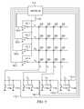
- a matrix or grid of touch sensitive switchescan be formed to provide a 2DCT sensor.
- a usercan then at a given time select one, or in some cases a plurality of, positions on a sensitive area.
- FIG. 5shows a two-dimensional touch sensor employing an array of sensors of the kind described with respect to FIGS. 3 and 4 .
- the charge measurement circuitis used in conjunction with drive circuits 101 . 1 , 101 . 2 , 101 . 3 , 101 . 4 and is arranged to drive different sensor points 205 .
- each of the drive circuits 101 . 1 , 101 . 2 , 101 . 3 , 101 . 4is controlled by the controller 118 to drive each of the corresponding lines X 1 , X 2 , X 3 , X 4 , using first control inputs 103 . 1 , 103 . 2 , 103 . 3 , 103 . 4 in the same way as the X plate 100 is driven in FIG. 3 and represented in FIG. 4 .
- an input 107provides a reference voltage “V”.
- the output of the coupling capacitors at each of the points 205are connected to one side of measuring capacitors Cs 112 . 1 , 112 . 2 , 112 . 3 , 112 . 4 which are arranged to measure an amount of charge present on the Y plate, Y 1 , Y 2 , Y 3 , Y 4 providing output signals 116 . 1 , 116 . 2 , 116 . 3 , 116 . 4 to detect the presence of an object in the same way as the operation of the circuit shown in FIG. 3 and FIG. 4 .
- FIG. 5some of the detail from FIG. 3 has been omitted for clarity.
- the resistor 140 , its switch 142 and actuating line 144are not shown.
- each of the switches 142can be commonly actuated by a single actuating line 144 from the controller 118 , since they only need to be switched together to perform their function described above.
- the controlleroperates as explained above to detect the presence of an object above one of the matrix of keys 205 , from a change in the capacitance of the keys, through a change in an amount of charge induced on the key during a burst of measurement cycles.
- the presence of a noise signalcan induce charge onto the keys of a touch sensor and provide a false detection or prevent a detection being made.
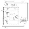
- FIG. 6shows timing diagrams 130 , 132 , 134 , 138 and 600 used to illustrate the further operation of the of the measurement circuit 108 shown in FIG. 3 to reduce the effects of noise according to an embodiment of the invention.
- the timing diagrams 130 , 132 , 134 and 138correspond to the same timing diagrams shown on FIG. 4 , except that the timing diagrams shown in FIG. 6 precede those shown in FIG. 4 , i.e. they run from t- 10 to t 1 .
- the same convention for each of the switches 110 and 114 shown in FIGS. 3 and 4is adopted here.
- the convention for the switch 142corresponding to the timing diagram 600 , is also shown in FIG. 3 .
- the control signal 144connects the SMP resistor 140 to either float (Z) or VDD depending on its position which is determined by the control line 144 . When the control line 144 is high (1) switch 142 connects SMP resistor 140 to the VDD. When the control line is low (0) switch 142 connects resistor 140 to float (Z).
- Timing diagram 600represents the control input applied to the switch 142 .
- the logical value of the control inputis shown, whereas on the right hand side the effect at the SMP resistor 140 is shown to be either “VDD” in which the resistor 142 is connected to VDD or float (Z) in which the resistor 142 is floated.
- the timing diagrams 130 , 132 , 134 , 138 and 600will now be described.
- the charge measurement circuit 108is initialized with both the control inputs for the switches 110 , 114 being high (1) so that both the Y plate and the charge measurement capacitor 112 are set to ground and the input to the switch 142 is set low (0) so that the resistor 140 is floated. This is to discharge the capacitor.
- the logical input to the control switch 114is set to zero, thereby opening the switch and floating the connecting point 114 . 1 which connects the output voltage 116 to one side of the measurement capacitor Cs 112 .
- the control input to the switch 142is set to high (1), thereby connecting the resistor 140 to VDD.
- the measurement capacitor Cs 112is now connected to ground at one side and to VDD via the SMP resistor 140 on the other side, thereby charging the capacitor.
- the measurement capacitor Cs 112is charged for a predetermined time T to charge Cs by a set amount. This direct charging of the measurement capacitor Cs bypassing the X drive circuit 101 is referred to as a pre-charging.
- the pre-charge on the capacitorcan be calculated, since the voltage, the value of the capacitor Cs 112 , the value of the resistor 140 and the charge time T are all known.
- VOUT 138shows the voltage of the capacitor between t- 8 and t- 7 .
- control input to the switch 142is set low (0) thereby floating the SMP resistor 140 .
- control input to switch 110is set low (0) thereby point 110 . 1 is floating.
- switches 110 , 114 and 142are driven in the same way as if they were collecting signal measurements, i.e. the same way as described with reference to FIG. 4 , with the exception that the X drive circuit 101 is not driven. Namely, as can be seen from FIG. 6 , the control switch to the X plate remains low (0) from time t- 10 to t 1 , so no voltage is applied to the X plate 100 of the coupling capacitor 105 . As a result, the charge accumulated on the measurement capacitor 112 is the pre-charge modulated by packets of charge picked up on the Y plate 104 of the coupling capacitor 105 during the acquisition cycles. This modulation will be a measure of noise, since it can only have been noise that has induced charge on the coupling capacitor 105 , given the absence of X drive signal during the dwell times of each cycle.
- a noise measurementis made by mimicking the signal measurement, but without driving the X plate 100 . Moreover, by pre-charging the accumulation capacitor before mimicking a normal signal measurement without driving the X plate, noise is measured through its modulation of the amount of charge initially placed on the charge accumulation capacitor by the pre-charge.
- the control input to the switch 114is set high (1) thereby grounding YB to transfer charge induced on the Y plate 104 of the key 105 , due to noise, onto the charge measurement capacitor 112 , until t- 4 when the control input to the switch 114 is set to low (0), which again floats the connecting point 114 . 1 .
- noiseis accumulated on the capacitor Cs as shown on VOUT 138 .
- the noise accumulated on the capacitor Cs during the dwell timecould result in the voltage at time t- 4 being higher or lower than the voltage at time t- 5 . Two different outcomes are illustrated in FIG.
- the control input to switch 110is set high (1), thereby grounding the connecting point 110 . 1 (YA), which is connected to the other side of the charge measurement capacitor Cs 112 . This will allow the charge on the capacitor Cs to be measured.
- the measurement of the charge accumulated on capacitor Csis carried out in the same manner as described above for measuring the charge accumulated on the capacitor due to a touch.
- the control input 144 to switch 142goes high (1), thereby connecting the SMP resistor to VDD.
- the voltage across the measurement capacitor Cs 112can be measured between times t- 2 and t- 1 .
- the amount of charge transferred from the Y plate 104 onto the measurement capacitor Cs 112 during the dwell time between t- 5 and t- 4 in addition to the pre-charged charge on the measurement capacitoris measured using the method described above.
- the read-out time Uis used to determine the amount of charge on the capacitor Cs, in addition to the capacitance of the capacitor Cs, which is known.
- the read-out time for each of the two outcomes represented by the solid line 602 and the dotted line 604will be different i.e. the time to discharge the measurement capacitor Cs for the scenario illustrated by the dotted line 604 will be higher than for the scenario represented by the solid line 602 .
- thesehave been shown having the same read-out time in FIG. 6 .
- control switch 114is set high (1) so that the timing diagram continues on to time t 1 as shown in FIG. 3 .
- the control input for switch 142is held low (0) during the measurement of the charge on the Y plate while the X plate is driven, as described above.
- the noise acquisitionprecedes the signal acquisition.
- the time sequenceis arbitrary.
- the measurementswill be interspersed, with for example one noise sample being taken followed by several signal samples and then another noise sample etc.
- the detected noiseis the difference between the charge on the measurement capacitor from the pre-charge cycle and the measured charge on the measurement capacitor after the dwell time. It will be appreciated that the charge on the capacitor after the dwell time could be less than or equal to the pre-charge charge, since charge can be removed from the capacitor as a result of the noise as well as being added. In other words the noise is a charge value that is obtained from subtracting the amount of charge on the measurement capacitor Cs 112 after the pre-charge step from the measured charge on the measurement capacitor Cs 112 after the dwell time. “Noise charge” will be used to identify this charge difference.
- noise factoris now calculated using the calculated noise charge.
- the detected noise charge from the current sample and the previous four samplesare used.
- the standard deviation of these 5 samplesis calculated. This will be referred to as the noise factor. It will be appreciated that it is computationally intensive to calculate a square root, so in the preferred embodiment the square of the standard deviation is used. It will be appreciated that more or less samples could be used to obtain the noise factor. Furthermore, it will be appreciated that other methods method for averaging the noise charge could be used.
- the method described abovehas shown how a noise factor can be calculated using the touch sensor and touch matrix shown in FIGS. 3 and 5 . Examples of how the noise factor is used to reduce the effects of noise in such an arrangement shown in FIGS. 3 and 5 are now described.
- the controller 118contains a single filter.
- the filtercould be any type of linear or non-linear filter, for example a low pass filter.
- the noise factoris used to control whether or not the filter is used. If the noise factor is below a specified threshold the filter is not used. However, if the noise factor is above a specified threshold the filter is applied to the measured signals. For example, if the touch matrix was implemented in a mobile phone, the noise factor during normal operation may fall below the specified value, thereby no filtering is used. However, if the mobile phone is connected to a phone charger during operation, for example, the phone charger may introduce noise. Therefore, if the noise factor due to the phone charger exceeds the specified value the filter would be applied to the measured signal. Once the phone battery is charged and the phone is disconnected from the charger the noise factor will again be below the specified value and the filter will not be applied to the measured signal.
- the embodiment of the inventionprovides a method for configuring one or more filters in response to real time noise signals present on the touch matrix.
- the sensing hardware shown in FIGS. 3 and 5typically remains unchanged. Therefore this may be implemented as a firmware update. Since, the method described above provides a method for activating or deactivating filters, when there is no noise source or the noise source is low i.e. below a specified value, the time taken to determine the location of a touch on a touch matrix can be increased, since there is no requirement for filtering.
- the controller 118may contain a low pass filter that can be configured using the acquired noise factor using the method described above.
- the frequency pass of the filtermay be adjusted based on the amount of noise detected. For example, if the expected signal level detected on the touch matrix is ‘S’, the frequency pass of the filter during normal operation could be ‘S’+10. However, if the detected noise signal is very high for example, then the frequency pass of the filter band could be increased to accommodate a signal with a greater amount of noise.
- the low pass filtercould be replaced with a slew rate limiter. The rate at which the input value is allowed to change is adapted in accordance with the noise factor.
- the slew rate limiteris adapted to allow signals that change more slowly, i.e. the allowed slew rate is low.
- the slew rate limiteris adapted to allow signals that change more quickly, i.e. the allow slew rate is high.
- slew rate limitercould be used other than a linear changing slew filter. For example where two consecutive samples exceed a predetermined value, the rate of change can be capped to a fixed increment or decrement so that the slew rate limiter can settle on the average value more quickly.
- a capacitive touch sensorfor detecting proximity and location of a body, the sensor comprising: one or multiple X lines; a plurality of Y lines each arranged to have a portion thereof adjacent to a portion of each of the X lines to form a plurality of sensing capacitors; a charge measurement capacitor connected to each Y line; one or more drive circuits arranged to drive respective ones of the X lines to enable charge transfer from the sensing capacitors associated with that X line to the respective measurement capacitors connected to the Y lines.
- the touch sensoris operable under control of a controller to measure a signal value in the usual way from one of the measurement capacitors, the signal value being indicative of the amount of charge transferred from one of the plurality of Y lines when actuating one of the respective X lines.
- the touch sensoris further operable under control of a controller to measure a noise value from one of the measurement capacitors indicative of the amount of charge transferred from one of the plurality of Y lines without first actuating one of the respective X lines. Charge is preferably injected onto the charge measurement capacitor before measuring the noise value, so that any noise contribution is accurately measured.
Landscapes
- Engineering & Computer Science (AREA)
- General Engineering & Computer Science (AREA)
- Theoretical Computer Science (AREA)
- Physics & Mathematics (AREA)
- General Physics & Mathematics (AREA)
- Human Computer Interaction (AREA)
- Measurement Of Resistance Or Impedance (AREA)
- Electronic Switches (AREA)
- Position Input By Displaying (AREA)
Abstract
Description
Claims (18)
Priority Applications (8)
| Application Number | Priority Date | Filing Date | Title |
|---|---|---|---|
| US12/255,998US8054090B2 (en) | 2008-10-22 | 2008-10-22 | Noise handling in capacitive touch sensors |
| CN2009801465179ACN102224485A (en) | 2008-10-22 | 2009-10-21 | Noise handling in capacitive touch sensors |
| DE112009002587TDE112009002587T5 (en) | 2008-10-22 | 2009-10-21 | Noise handling in capacitive touch sensors |
| PCT/US2009/061543WO2010048331A1 (en) | 2008-10-22 | 2009-10-21 | Noise handling in capacitive touch sensors |
| TW098135833ATW201030585A (en) | 2008-10-22 | 2009-10-22 | Noise handling in capacitive touch sensors |
| US13/290,931US8598894B2 (en) | 2008-10-22 | 2011-11-07 | Noise handling in capacitive touch sensors |
| US13/945,820US8629686B2 (en) | 2008-10-22 | 2013-07-18 | Noise measurement in capacitive touch sensors |
| US14/153,821US9448267B2 (en) | 2008-10-22 | 2014-01-13 | Noise measurement in capacitive touch sensors |
Applications Claiming Priority (1)
| Application Number | Priority Date | Filing Date | Title |
|---|---|---|---|
| US12/255,998US8054090B2 (en) | 2008-10-22 | 2008-10-22 | Noise handling in capacitive touch sensors |
Related Child Applications (1)
| Application Number | Title | Priority Date | Filing Date |
|---|---|---|---|
| US13/290,931ContinuationUS8598894B2 (en) | 2008-10-22 | 2011-11-07 | Noise handling in capacitive touch sensors |
Publications (2)
| Publication Number | Publication Date |
|---|---|
| US20100097078A1 US20100097078A1 (en) | 2010-04-22 |
| US8054090B2true US8054090B2 (en) | 2011-11-08 |
Family
ID=41427467
Family Applications (4)
| Application Number | Title | Priority Date | Filing Date |
|---|---|---|---|
| US12/255,998Active2030-01-10US8054090B2 (en) | 2008-10-22 | 2008-10-22 | Noise handling in capacitive touch sensors |
| US13/290,931Active2029-03-01US8598894B2 (en) | 2008-10-22 | 2011-11-07 | Noise handling in capacitive touch sensors |
| US13/945,820ActiveUS8629686B2 (en) | 2008-10-22 | 2013-07-18 | Noise measurement in capacitive touch sensors |
| US14/153,821Active2028-12-14US9448267B2 (en) | 2008-10-22 | 2014-01-13 | Noise measurement in capacitive touch sensors |
Family Applications After (3)
| Application Number | Title | Priority Date | Filing Date |
|---|---|---|---|
| US13/290,931Active2029-03-01US8598894B2 (en) | 2008-10-22 | 2011-11-07 | Noise handling in capacitive touch sensors |
| US13/945,820ActiveUS8629686B2 (en) | 2008-10-22 | 2013-07-18 | Noise measurement in capacitive touch sensors |
| US14/153,821Active2028-12-14US9448267B2 (en) | 2008-10-22 | 2014-01-13 | Noise measurement in capacitive touch sensors |
Country Status (5)
| Country | Link |
|---|---|
| US (4) | US8054090B2 (en) |
| CN (1) | CN102224485A (en) |
| DE (1) | DE112009002587T5 (en) |
| TW (1) | TW201030585A (en) |
| WO (1) | WO2010048331A1 (en) |
Cited By (12)
| Publication number | Priority date | Publication date | Assignee | Title |
|---|---|---|---|---|
| US20110157077A1 (en)* | 2008-06-25 | 2011-06-30 | Bradley Martin | Capacitive sensor system with noise reduction |
| US20130141346A1 (en)* | 2011-12-06 | 2013-06-06 | Samsung Electronics Co. Ltd. | Method and apparatus for configuring touch sensing parameters |
| US8729911B2 (en) | 2011-04-19 | 2014-05-20 | Cypress Semiconductor Corporation | Usage of weighting matrices in multi-phase scanning modes |
| US20140267059A1 (en)* | 2013-03-12 | 2014-09-18 | Motorola Mobility Llc | Adaptive Touch Sensor Control Based on Identification of Attached Accessory |
| US8860682B1 (en) | 2013-04-22 | 2014-10-14 | Cypress Semiconductor Corporation | Hardware de-convolution block for multi-phase scanning |
| US9013441B2 (en) | 2010-08-24 | 2015-04-21 | Cypress Semiconductor Corporation | Smart scanning for a capacitive sensing array |
| US9013195B2 (en) | 2010-08-23 | 2015-04-21 | Cypress Semiconductor Corporation | Mutual capacitance sensing circuits, methods and systems |
| US9244550B2 (en) | 2013-08-16 | 2016-01-26 | Blackberry Limited | Electronic device and method of identifying frequency for detecting touches |
| US9442146B2 (en) | 2009-03-26 | 2016-09-13 | Parade Technologies, Ltd. | Multi-mode capacitive sensing device and method with current conveyor |
| US9448267B2 (en) | 2008-10-22 | 2016-09-20 | Atmel Corporation | Noise measurement in capacitive touch sensors |
| US9811213B2 (en) | 2013-03-15 | 2017-11-07 | Synaptics Incorporated | Systems and methods for input device noise mitigation via a touch buffer |
| US11320946B2 (en) | 2011-04-19 | 2022-05-03 | Cypress Semiconductor Corporation | Capacitive panel scanning with reduced number of sensing circuits |
Families Citing this family (54)
| Publication number | Priority date | Publication date | Assignee | Title |
|---|---|---|---|---|
| WO2010012820A2 (en)* | 2008-07-31 | 2010-02-04 | Ident Technology Ag | Operating unit for electrical appliances |
| DE102008044908A1 (en)* | 2008-08-29 | 2010-03-04 | Lemförder Electronic GmbH | Arrangement for measuring at least one value of a voltage applied to an electronic component voltage |
| FR2938656B1 (en)* | 2008-11-18 | 2011-08-26 | Thales Sa | INTRINSIC SECURITY SYSTEM AND TEST MODULE, IN PARTICULAR FOR USE IN A RAILWAY SIGNALING SYSTEM |
| DE102010001377A1 (en)* | 2010-01-29 | 2011-08-04 | E.G.O. Elektro-Gerätebau GmbH, 75038 | Circuit arrangement for determining a capacitance of a number of capacitive sensor elements |
| US8564311B2 (en)* | 2010-07-01 | 2013-10-22 | Stmicroelectronics Asia Pacific Pte Ltd. | Sensing phase sequence to suppress single tone noise |
| KR101394937B1 (en) | 2010-09-07 | 2014-05-15 | 엘지디스플레이 주식회사 | Display device having touch sensor and method for driving the same |
| JP5563722B2 (en)* | 2010-09-14 | 2014-07-30 | アドヴァンスト・シリコン・ソシエテ・アノニム | Circuits for capacitive touch applications |
| US9459736B2 (en)* | 2010-10-12 | 2016-10-04 | Parade Technologies, Ltd. | Flexible capacitive sensor array |
| US9454268B2 (en) | 2010-10-12 | 2016-09-27 | Parade Technologies, Ltd. | Force sensing capacitive hybrid touch sensor |
| JP5307110B2 (en)* | 2010-12-01 | 2013-10-02 | 株式会社ジャパンディスプレイ | Touch panel |
| WO2012108911A1 (en) | 2011-02-07 | 2012-08-16 | Cypress Semiconductor Corporation | Noise filtering devices, systems and methods for capacitance sensing devices |
| US9030421B2 (en)* | 2011-04-01 | 2015-05-12 | Qualcomm Incorporated | Touchscreen controller with adjustable parameters |
| US8427452B2 (en) | 2011-05-31 | 2013-04-23 | Pixart Imaging, Inc. | Charge pump frequency selection in touch screen sensor interface system |
| US20130106759A1 (en)* | 2011-10-27 | 2013-05-02 | Einar Fredriksen | Narrow-Band Touch Detection |
| EP2774253A2 (en)* | 2011-11-01 | 2014-09-10 | Frederick Johannes Bruwer | Capacitive sensing enabled switch mode power supply and data transfer |
| TW201324246A (en)* | 2011-12-07 | 2013-06-16 | Ene Technology Inc | Point reporting device and point reporting method |
| JP5809991B2 (en)* | 2012-01-23 | 2015-11-11 | 株式会社ジャパンディスプレイ | Display device |
| US9444452B2 (en)* | 2012-02-24 | 2016-09-13 | Parade Technologies, Ltd. | Frequency hopping algorithm for capacitance sensing devices |
| CN103309529B (en)* | 2012-03-16 | 2016-10-05 | 联想(北京)有限公司 | A kind of capacitance touch screen and the method identifying touch signal thereof |
| KR101378511B1 (en)* | 2012-03-28 | 2014-03-27 | 주식회사 하이딥 | Method, touch sensing apparatus and computer-readable recording medium for minimizing noise on touch panel |
| US9921691B2 (en)* | 2012-05-18 | 2018-03-20 | Atmel Corporation | Burst-mode self-capacitance measurement with compensated capacitance |
| CN103455188A (en)* | 2012-06-01 | 2013-12-18 | 群康科技(深圳)有限公司 | Touch signal generating method and touch display |
| US9092101B2 (en)* | 2012-06-26 | 2015-07-28 | Google Technology Holdings LLC | Battery charging interrupt |
| CN103516441B (en)* | 2012-06-26 | 2016-03-02 | 上海东软载波微电子有限公司 | Capacitive touch screen anti-noise method and touch chip |
| CN102788910B (en)* | 2012-06-29 | 2016-03-16 | 敦泰科技有限公司 | Noise detection, scanning and frequency hopping method of mutual capacitance touch screen |
| US9236861B2 (en) | 2012-07-02 | 2016-01-12 | Stmicroelectronics Asia Pacific Pte Ltd | Capacitive proximity sensor with enabled touch detection |
| US9176597B2 (en)* | 2012-07-02 | 2015-11-03 | Stmicroelectronics Asia Pacific Pte Ltd | Directional capacitive proximity sensor with bootstrapping |
| KR101931737B1 (en)* | 2012-07-17 | 2018-12-26 | 삼성디스플레이 주식회사 | Touch Screen Panel and Driving Method Thereof |
| US9164629B2 (en) | 2012-08-06 | 2015-10-20 | Stmicroelectronics Asia Pacific Pte Ltd | Touch screen panel with slide feature |
| WO2014057569A1 (en)* | 2012-10-12 | 2014-04-17 | Nltテクノロジー株式会社 | Electronic device, capacitance sensor, and touch panel |
| CN102968230B (en)* | 2012-11-07 | 2017-07-28 | 江苏美琪威电子科技有限公司 | Method for eliminating noise of capacitive touch screen and capacitive touch screen |
| KR101455315B1 (en)* | 2012-11-13 | 2014-10-27 | 엘지디스플레이 주식회사 | Display device with integrated touch screen and method for driving the same |
| CN103134996B (en)* | 2013-01-31 | 2015-12-09 | 珠海中慧微电子有限公司 | Adopt mutual capacitance sensing circuit and the method for charge compensation |
| US8874396B1 (en) | 2013-06-28 | 2014-10-28 | Cypress Semiconductor Corporation | Injected touch noise analysis |
| US9367190B2 (en)* | 2013-09-13 | 2016-06-14 | Apex Material Technology Corp. | Touch recognition method and system for a capacitive touch apparatus |
| TWI512584B (en)* | 2013-11-06 | 2015-12-11 | Apex Material Technology Corp | Touch sensitive control device, electronic apparatus and method thereof |
| US9274649B2 (en) | 2013-11-06 | 2016-03-01 | Apex Material Technology Corp. | Handling of electromagnetic interference in an electronic apparatus |
| US9164137B2 (en)* | 2013-12-05 | 2015-10-20 | Parade Technologies, Ltd. | Tunable baseline compensation scheme for touchscreen controllers |
| JP6219182B2 (en)* | 2014-01-29 | 2017-10-25 | アルプス電気株式会社 | Input device |
| US9454272B2 (en) | 2014-05-22 | 2016-09-27 | Stmicroelectronics Asia Pacific Pte Ltd | Touch screen for stylus emitting wireless signals |
| DE102014218535A1 (en)* | 2014-09-16 | 2016-03-17 | Robert Bosch Gmbh | Capacitive sensor |
| US9818367B2 (en)* | 2015-03-17 | 2017-11-14 | Apple Inc. | Content-driven slew rate control for display driver |
| CN106249970B (en)* | 2015-06-05 | 2020-11-27 | 恩智浦美国有限公司 | Capacitive sensor with noise suppression |
| US9874983B2 (en)* | 2015-06-23 | 2018-01-23 | Synaptics Incorporated | Electrode combining for noise determination |
| US10613643B2 (en) | 2015-06-25 | 2020-04-07 | Apple Inc. | Method for stylus touch-down and lift-off noise mitigation |
| JP6513513B2 (en)* | 2015-07-09 | 2019-05-15 | アルプスアルパイン株式会社 | INPUT DEVICE, ITS CONTROL METHOD, AND PROGRAM |
| US20170046005A1 (en)* | 2015-08-12 | 2017-02-16 | Cirque Corporation | Avoiding noise when using multiple capacitive measuring integrated circuits |
| DE102016109799B4 (en)* | 2016-05-27 | 2017-12-14 | Infineon Technologies Ag | Communication devices, methods for detecting an edge in a received signal and method for receiving data |
| EP3622256A4 (en) | 2017-05-12 | 2020-05-13 | Texas Instruments Incorporated | CAPACITIVE SENSOR ENCODER AND METHOD |
| WO2018205261A1 (en) | 2017-05-12 | 2018-11-15 | Texas Instruments Incorporated | Methods and apparatus to determine a position of a rotatable shaft of a motor |
| JP7006189B2 (en)* | 2017-11-28 | 2022-01-24 | 株式会社アイシン | Capacitance detector |
| US10338746B1 (en) | 2018-01-18 | 2019-07-02 | Stmicroelectronics Asia Pacific Pte Ltd | Mutual capacitance sensing using magnitude noise sensing with sine and cosine multipliers |
| FR3085540B1 (en)* | 2018-08-31 | 2020-09-25 | St Microelectronics Rousset | INTEGRATED DEVICE FOR TEMPORAL MEASUREMENT WITH ULTRA LONG TIME CONSTANT AND MANUFACTURING PROCESS |
| CN115701571A (en)* | 2021-08-02 | 2023-02-10 | 维沃移动通信有限公司 | Touch position determination method, device and electronic equipment |
Citations (5)
| Publication number | Priority date | Publication date | Assignee | Title |
|---|---|---|---|---|
| WO2000044018A1 (en) | 1999-01-26 | 2000-07-27 | Harald Philipp | Capacitive sensor and array |
| US20020186210A1 (en) | 2001-06-07 | 2002-12-12 | Alps Electric Co., Ltd | Coordinate input device |
| US20050099188A1 (en)* | 2002-07-02 | 2005-05-12 | Baxter Larry K. | Capacitive measurement system |
| US7663607B2 (en) | 2004-05-06 | 2010-02-16 | Apple Inc. | Multipoint touchscreen |
| US7920129B2 (en) | 2007-01-03 | 2011-04-05 | Apple Inc. | Double-sided touch-sensitive panel with shield and drive combined layer |
Family Cites Families (24)
| Publication number | Priority date | Publication date | Assignee | Title |
|---|---|---|---|---|
| US4831566A (en) | 1987-03-20 | 1989-05-16 | Summagraphics Corporation | Method and apparatus for calibration of a charge ratio digitizer |
| JP5395429B2 (en)* | 2005-06-03 | 2014-01-22 | シナプティクス インコーポレイテッド | Method and system for detecting capacitance using sigma delta measurement |
| US7288946B2 (en)* | 2005-06-03 | 2007-10-30 | Synaptics Incorporated | Methods and systems for detecting a capacitance using sigma-delta measurement techniques |
| JP4618026B2 (en) | 2005-07-12 | 2011-01-26 | ソニー株式会社 | Display device and detection method using display device for displaying and receiving light |
| EP1746488A2 (en) | 2005-07-21 | 2007-01-24 | TPO Displays Corp. | Electromagnetic digitizer sensor array structure |
| US8049732B2 (en) | 2007-01-03 | 2011-11-01 | Apple Inc. | Front-end signal compensation |
| US8031174B2 (en) | 2007-01-03 | 2011-10-04 | Apple Inc. | Multi-touch surface stackup arrangement |
| TW200842681A (en) | 2007-04-27 | 2008-11-01 | Tpk Touch Solutions Inc | Touch pattern structure of a capacitive touch panel |
| TW200844827A (en) | 2007-05-11 | 2008-11-16 | Sense Pad Tech Co Ltd | Transparent touch panel device |
| US8040326B2 (en) | 2007-06-13 | 2011-10-18 | Apple Inc. | Integrated in-plane switching display and touch sensor |
| JP4506785B2 (en) | 2007-06-14 | 2010-07-21 | エプソンイメージングデバイス株式会社 | Capacitive input device |
| WO2009016382A2 (en)* | 2007-07-31 | 2009-02-05 | Qrg Limited | Sensor and method of sensing |
| KR101720919B1 (en) | 2008-02-28 | 2017-03-28 | 쓰리엠 이노베이티브 프로퍼티즈 컴파니 | Touch screen sensor |
| US7863909B2 (en)* | 2008-03-04 | 2011-01-04 | Synaptics Incorporated | System and method for measuring a capacitance by transferring charge from a fixed source |
| JP4720857B2 (en) | 2008-06-18 | 2011-07-13 | ソニー株式会社 | Capacitance type input device and display device with input function |
| US8054090B2 (en) | 2008-10-22 | 2011-11-08 | Atmel Corporation | Noise handling in capacitive touch sensors |
| US8031094B2 (en) | 2009-09-11 | 2011-10-04 | Apple Inc. | Touch controller with improved analog front end |
| WO2012129247A2 (en) | 2011-03-21 | 2012-09-27 | Apple Inc. | Electronic devices with flexible displays |
| US8934228B2 (en) | 2011-03-21 | 2015-01-13 | Apple Inc. | Display-based speaker structures for electronic devices |
| US9866660B2 (en) | 2011-03-21 | 2018-01-09 | Apple Inc. | Electronic devices with concave displays |
| US8816977B2 (en) | 2011-03-21 | 2014-08-26 | Apple Inc. | Electronic devices with flexible displays |
| US9178970B2 (en) | 2011-03-21 | 2015-11-03 | Apple Inc. | Electronic devices with convex displays |
| US8665236B2 (en) | 2011-09-26 | 2014-03-04 | Apple Inc. | Electronic device with wrap around display |
| US8723824B2 (en) | 2011-09-27 | 2014-05-13 | Apple Inc. | Electronic devices with sidewall displays |
- 2008
- 2008-10-22USUS12/255,998patent/US8054090B2/enactiveActive
- 2009
- 2009-10-21DEDE112009002587Tpatent/DE112009002587T5/ennot_activeCeased
- 2009-10-21WOPCT/US2009/061543patent/WO2010048331A1/enactiveApplication Filing
- 2009-10-21CNCN2009801465179Apatent/CN102224485A/enactivePending
- 2009-10-22TWTW098135833Apatent/TW201030585A/enunknown
- 2011
- 2011-11-07USUS13/290,931patent/US8598894B2/enactiveActive
- 2013
- 2013-07-18USUS13/945,820patent/US8629686B2/enactiveActive
- 2014
- 2014-01-13USUS14/153,821patent/US9448267B2/enactiveActive
Patent Citations (6)
| Publication number | Priority date | Publication date | Assignee | Title |
|---|---|---|---|---|
| WO2000044018A1 (en) | 1999-01-26 | 2000-07-27 | Harald Philipp | Capacitive sensor and array |
| US6452514B1 (en) | 1999-01-26 | 2002-09-17 | Harald Philipp | Capacitive sensor and array |
| US20020186210A1 (en) | 2001-06-07 | 2002-12-12 | Alps Electric Co., Ltd | Coordinate input device |
| US20050099188A1 (en)* | 2002-07-02 | 2005-05-12 | Baxter Larry K. | Capacitive measurement system |
| US7663607B2 (en) | 2004-05-06 | 2010-02-16 | Apple Inc. | Multipoint touchscreen |
| US7920129B2 (en) | 2007-01-03 | 2011-04-05 | Apple Inc. | Double-sided touch-sensitive panel with shield and drive combined layer |
Non-Patent Citations (2)
| Title |
|---|
| "International Application Serial No. PCT/US2009/061543, Search Report mailed Jan. 7, 2010", 3 pgs. |
| "International Application Serial No. PCT/US2009/061543, Written Opinion mailed Jan. 7, 2010", 4 pgs. |
Cited By (15)
| Publication number | Priority date | Publication date | Assignee | Title |
|---|---|---|---|---|
| US20110157077A1 (en)* | 2008-06-25 | 2011-06-30 | Bradley Martin | Capacitive sensor system with noise reduction |
| US8941394B2 (en)* | 2008-06-25 | 2015-01-27 | Silicon Laboratories Inc. | Capacitive sensor system with noise reduction |
| US9448267B2 (en) | 2008-10-22 | 2016-09-20 | Atmel Corporation | Noise measurement in capacitive touch sensors |
| US9442146B2 (en) | 2009-03-26 | 2016-09-13 | Parade Technologies, Ltd. | Multi-mode capacitive sensing device and method with current conveyor |
| US9013195B2 (en) | 2010-08-23 | 2015-04-21 | Cypress Semiconductor Corporation | Mutual capacitance sensing circuits, methods and systems |
| US9013441B2 (en) | 2010-08-24 | 2015-04-21 | Cypress Semiconductor Corporation | Smart scanning for a capacitive sensing array |
| US8729911B2 (en) | 2011-04-19 | 2014-05-20 | Cypress Semiconductor Corporation | Usage of weighting matrices in multi-phase scanning modes |
| US11320946B2 (en) | 2011-04-19 | 2022-05-03 | Cypress Semiconductor Corporation | Capacitive panel scanning with reduced number of sensing circuits |
| US20130141346A1 (en)* | 2011-12-06 | 2013-06-06 | Samsung Electronics Co. Ltd. | Method and apparatus for configuring touch sensing parameters |
| US20140267059A1 (en)* | 2013-03-12 | 2014-09-18 | Motorola Mobility Llc | Adaptive Touch Sensor Control Based on Identification of Attached Accessory |
| US9041671B2 (en)* | 2013-03-12 | 2015-05-26 | Google Technology Holdings LLC | Adaptive touch sensor control based on identification of attached accessory |
| US9811213B2 (en) | 2013-03-15 | 2017-11-07 | Synaptics Incorporated | Systems and methods for input device noise mitigation via a touch buffer |
| US9377493B2 (en) | 2013-04-22 | 2016-06-28 | Parade Technologies, Ltd. | Hardware de-convolution block for multi-phase scanning |
| US8860682B1 (en) | 2013-04-22 | 2014-10-14 | Cypress Semiconductor Corporation | Hardware de-convolution block for multi-phase scanning |
| US9244550B2 (en) | 2013-08-16 | 2016-01-26 | Blackberry Limited | Electronic device and method of identifying frequency for detecting touches |
Also Published As
| Publication number | Publication date |
|---|---|
| US20100097078A1 (en) | 2010-04-22 |
| US8598894B2 (en) | 2013-12-03 |
| US20120049859A1 (en) | 2012-03-01 |
| DE112009002587T5 (en) | 2012-08-02 |
| US20140300376A1 (en) | 2014-10-09 |
| CN102224485A (en) | 2011-10-19 |
| US8629686B2 (en) | 2014-01-14 |
| WO2010048331A1 (en) | 2010-04-29 |
| US9448267B2 (en) | 2016-09-20 |
| TW201030585A (en) | 2010-08-16 |
| US20130307569A1 (en) | 2013-11-21 |
Similar Documents
| Publication | Publication Date | Title |
|---|---|---|
| US8054090B2 (en) | Noise handling in capacitive touch sensors | |
| US8605037B2 (en) | Noise reduction in capacitive touch sensors | |
| US9569037B2 (en) | Capacitive sensing with low-frequency noise reduction | |
| US8378981B2 (en) | Capacitive sensing with high-frequency noise reduction | |
| US8976151B2 (en) | Configurable analog front-end for mutual capacitance sensing and self capacitance sensing | |
| US9600124B2 (en) | Sensor and method of sensing | |
| US8552995B2 (en) | Sensor and method of sensing | |
| TWI506513B (en) | Method and apparatus to measure self-capacitance using a single pin | |
| US8248383B2 (en) | Multi-touch touch screen with single-layer ITO bars arranged in parallel | |
| US8854107B2 (en) | Integrator circuit with inverting integrator and non-inverting integrator | |
| US8937611B2 (en) | Capacitive touch sensors | |
| US9547399B2 (en) | Injected touch noise analysis | |
| US10068121B2 (en) | Baseline compensation for capacitive sensing | |
| US8174273B2 (en) | Capacitance measurement circuit with dynamic feedback | |
| TWI466028B (en) | Integrator circuit with inverting integrator and non-inverting integrator | |
| WO2016028387A1 (en) | Providing a baseline capacitance for a capacitance sensing channel | |
| CN114355056A (en) | Capacitance measuring circuit, capacitance measuring system, touch device and electronic equipment | |
| CN109643191A (en) | Detection method of touch and touch detection device | |
| WO2015038177A1 (en) | High resolution capacitance to code converter | |
| EP2722985A1 (en) | Method of differential measurement of voltage levels of capacitive change |
Legal Events
| Date | Code | Title | Description |
|---|---|---|---|
| AS | Assignment | Owner name:ATMEL CORPORATION,CALIFORNIA Free format text:ASSIGNMENT OF ASSIGNORS INTEREST;ASSIGNOR:QRG LIMITED;REEL/FRAME:022610/0350 Effective date:20090203 Owner name:ATMEL CORPORATION,CALIFORNIA Free format text:ASSIGNMENT OF ASSIGNORS INTEREST;ASSIGNOR:QRG LIMITED;REEL/FRAME:022783/0804 Effective date:20090203 Owner name:ATMEL CORPORATION, CALIFORNIA Free format text:ASSIGNMENT OF ASSIGNORS INTEREST;ASSIGNOR:QRG LIMITED;REEL/FRAME:022610/0350 Effective date:20090203 Owner name:ATMEL CORPORATION, CALIFORNIA Free format text:ASSIGNMENT OF ASSIGNORS INTEREST;ASSIGNOR:QRG LIMITED;REEL/FRAME:022783/0804 Effective date:20090203 | |
| AS | Assignment | Owner name:QRG LIMITED,UNITED KINGDOM Free format text:ASSIGNMENT OF ASSIGNORS INTEREST;ASSIGNORS:PHILIPP, HARALD;YILMAZ, ESAT;PICKETT, DANIEL;SIGNING DATES FROM 20091126 TO 20091130;REEL/FRAME:023647/0797 Owner name:QRG LIMITED, UNITED KINGDOM Free format text:ASSIGNMENT OF ASSIGNORS INTEREST;ASSIGNORS:PHILIPP, HARALD;YILMAZ, ESAT;PICKETT, DANIEL;SIGNING DATES FROM 20091126 TO 20091130;REEL/FRAME:023647/0797 | |
| AS | Assignment | Owner name:ATMEL CORPORATION,CALIFORNIA Free format text:ASSIGNMENT OF ASSIGNORS INTEREST;ASSIGNOR:QRG LIMITED;REEL/FRAME:023656/0538 Effective date:20091211 Owner name:ATMEL CORPORATION, CALIFORNIA Free format text:ASSIGNMENT OF ASSIGNORS INTEREST;ASSIGNOR:QRG LIMITED;REEL/FRAME:023656/0538 Effective date:20091211 | |
| STCF | Information on status: patent grant | Free format text:PATENTED CASE | |
| AS | Assignment | Owner name:MORGAN STANLEY SENIOR FUNDING, INC. AS ADMINISTRATIVE AGENT, NEW YORK Free format text:PATENT SECURITY AGREEMENT;ASSIGNOR:ATMEL CORPORATION;REEL/FRAME:031912/0173 Effective date:20131206 Owner name:MORGAN STANLEY SENIOR FUNDING, INC. AS ADMINISTRAT Free format text:PATENT SECURITY AGREEMENT;ASSIGNOR:ATMEL CORPORATION;REEL/FRAME:031912/0173 Effective date:20131206 | |
| FPAY | Fee payment | Year of fee payment:4 | |
| AS | Assignment | Owner name:ATMEL CORPORATION, CALIFORNIA Free format text:TERMINATION AND RELEASE OF SECURITY INTEREST IN PATENT COLLATERAL;ASSIGNOR:MORGAN STANLEY SENIOR FUNDING, INC.;REEL/FRAME:038376/0001 Effective date:20160404 | |
| AS | Assignment | Owner name:JPMORGAN CHASE BANK, N.A., AS ADMINISTRATIVE AGENT, ILLINOIS Free format text:SECURITY INTEREST;ASSIGNOR:ATMEL CORPORATION;REEL/FRAME:041715/0747 Effective date:20170208 Owner name:JPMORGAN CHASE BANK, N.A., AS ADMINISTRATIVE AGENT Free format text:SECURITY INTEREST;ASSIGNOR:ATMEL CORPORATION;REEL/FRAME:041715/0747 Effective date:20170208 | |
| AS | Assignment | Owner name:JPMORGAN CHASE BANK, N.A., AS ADMINISTRATIVE AGENT, ILLINOIS Free format text:SECURITY INTEREST;ASSIGNORS:MICROCHIP TECHNOLOGY INCORPORATED;SILICON STORAGE TECHNOLOGY, INC.;ATMEL CORPORATION;AND OTHERS;REEL/FRAME:046426/0001 Effective date:20180529 Owner name:JPMORGAN CHASE BANK, N.A., AS ADMINISTRATIVE AGENT Free format text:SECURITY INTEREST;ASSIGNORS:MICROCHIP TECHNOLOGY INCORPORATED;SILICON STORAGE TECHNOLOGY, INC.;ATMEL CORPORATION;AND OTHERS;REEL/FRAME:046426/0001 Effective date:20180529 | |
| AS | Assignment | Owner name:WELLS FARGO BANK, NATIONAL ASSOCIATION, AS NOTES COLLATERAL AGENT, CALIFORNIA Free format text:SECURITY INTEREST;ASSIGNORS:MICROCHIP TECHNOLOGY INCORPORATED;SILICON STORAGE TECHNOLOGY, INC.;ATMEL CORPORATION;AND OTHERS;REEL/FRAME:047103/0206 Effective date:20180914 Owner name:WELLS FARGO BANK, NATIONAL ASSOCIATION, AS NOTES C Free format text:SECURITY INTEREST;ASSIGNORS:MICROCHIP TECHNOLOGY INCORPORATED;SILICON STORAGE TECHNOLOGY, INC.;ATMEL CORPORATION;AND OTHERS;REEL/FRAME:047103/0206 Effective date:20180914 | |
| AS | Assignment | Owner name:MICROCHIP TECHNOLOGY INCORPORATED, ARIZONA Free format text:RELEASE OF SECURITY INTEREST IN CERTAIN PATENT RIGHTS;ASSIGNOR:WELLS FARGO BANK, NATIONAL ASSOCIATION, AS NOTES COLLATERAL AGENT;REEL/FRAME:047976/0937 Effective date:20181221 Owner name:ATMEL CORPORATION, ARIZONA Free format text:RELEASE OF SECURITY INTEREST IN CERTAIN PATENT RIGHTS;ASSIGNOR:JPMORGAN CHASE BANK, N.A., AS ADMINISTRATIVE AGENT;REEL/FRAME:047976/0884 Effective date:20181221 Owner name:MICROCHIP TECHNOLOGY INCORPORATED, ARIZONA Free format text:RELEASE OF SECURITY INTEREST IN CERTAIN PATENT RIGHTS;ASSIGNOR:JPMORGAN CHASE BANK, N.A., AS ADMINISTRATIVE AGENT;REEL/FRAME:047976/0884 Effective date:20181221 Owner name:ATMEL CORPORATION, ARIZONA Free format text:RELEASE OF SECURITY INTEREST IN CERTAIN PATENT RIGHTS;ASSIGNOR:WELLS FARGO BANK, NATIONAL ASSOCIATION, AS NOTES COLLATERAL AGENT;REEL/FRAME:047976/0937 Effective date:20181221 | |
| AS | Assignment | Owner name:NEODRON LIMITED, IRELAND Free format text:ASSIGNMENT OF ASSIGNORS INTEREST;ASSIGNORS:MICROCHIP TECHNOLOGY INC.;ATMEL CORPORATION;MICROCHIP TECHNOLOGY GERMANY GMBH;REEL/FRAME:048259/0840 Effective date:20181221 | |
| MAFP | Maintenance fee payment | Free format text:PAYMENT OF MAINTENANCE FEE, 8TH YEAR, LARGE ENTITY (ORIGINAL EVENT CODE: M1552); ENTITY STATUS OF PATENT OWNER: LARGE ENTITY Year of fee payment:8 | |
| AS | Assignment | Owner name:MICROSEMI STORAGE SOLUTIONS, INC., ARIZONA Free format text:RELEASE BY SECURED PARTY;ASSIGNOR:JPMORGAN CHASE BANK, N.A., AS ADMINISTRATIVE AGENT;REEL/FRAME:059333/0222 Effective date:20220218 Owner name:MICROSEMI CORPORATION, ARIZONA Free format text:RELEASE BY SECURED PARTY;ASSIGNOR:JPMORGAN CHASE BANK, N.A., AS ADMINISTRATIVE AGENT;REEL/FRAME:059333/0222 Effective date:20220218 Owner name:ATMEL CORPORATION, ARIZONA Free format text:RELEASE BY SECURED PARTY;ASSIGNOR:JPMORGAN CHASE BANK, N.A., AS ADMINISTRATIVE AGENT;REEL/FRAME:059333/0222 Effective date:20220218 Owner name:SILICON STORAGE TECHNOLOGY, INC., ARIZONA Free format text:RELEASE BY SECURED PARTY;ASSIGNOR:JPMORGAN CHASE BANK, N.A., AS ADMINISTRATIVE AGENT;REEL/FRAME:059333/0222 Effective date:20220218 Owner name:MICROCHIP TECHNOLOGY INCORPORATED, ARIZONA Free format text:RELEASE BY SECURED PARTY;ASSIGNOR:JPMORGAN CHASE BANK, N.A., AS ADMINISTRATIVE AGENT;REEL/FRAME:059333/0222 Effective date:20220218 | |
| AS | Assignment | Owner name:ATMEL CORPORATION, ARIZONA Free format text:RELEASE BY SECURED PARTY;ASSIGNOR:JPMORGAN CHASE BANK, N.A., AS ADMINISTRATIVE AGENT;REEL/FRAME:059262/0105 Effective date:20220218 | |
| AS | Assignment | Owner name:MICROSEMI STORAGE SOLUTIONS, INC., ARIZONA Free format text:RELEASE BY SECURED PARTY;ASSIGNOR:WELLS FARGO BANK, NATIONAL ASSOCIATION, AS NOTES COLLATERAL AGENT;REEL/FRAME:059358/0001 Effective date:20220228 Owner name:MICROSEMI CORPORATION, ARIZONA Free format text:RELEASE BY SECURED PARTY;ASSIGNOR:WELLS FARGO BANK, NATIONAL ASSOCIATION, AS NOTES COLLATERAL AGENT;REEL/FRAME:059358/0001 Effective date:20220228 Owner name:ATMEL CORPORATION, ARIZONA Free format text:RELEASE BY SECURED PARTY;ASSIGNOR:WELLS FARGO BANK, NATIONAL ASSOCIATION, AS NOTES COLLATERAL AGENT;REEL/FRAME:059358/0001 Effective date:20220228 Owner name:SILICON STORAGE TECHNOLOGY, INC., ARIZONA Free format text:RELEASE BY SECURED PARTY;ASSIGNOR:WELLS FARGO BANK, NATIONAL ASSOCIATION, AS NOTES COLLATERAL AGENT;REEL/FRAME:059358/0001 Effective date:20220228 Owner name:MICROCHIP TECHNOLOGY INCORPORATED, ARIZONA Free format text:RELEASE BY SECURED PARTY;ASSIGNOR:WELLS FARGO BANK, NATIONAL ASSOCIATION, AS NOTES COLLATERAL AGENT;REEL/FRAME:059358/0001 Effective date:20220228 | |
| MAFP | Maintenance fee payment | Free format text:PAYMENT OF MAINTENANCE FEE, 12TH YEAR, LARGE ENTITY (ORIGINAL EVENT CODE: M1553); ENTITY STATUS OF PATENT OWNER: LARGE ENTITY Year of fee payment:12 |