US8052931B2 - Ultra low-power CMOS based bio-sensor circuit - Google Patents
Ultra low-power CMOS based bio-sensor circuitDownload PDFInfo
- Publication number
- US8052931B2 US8052931B2US12/651,504US65150410AUS8052931B2US 8052931 B2US8052931 B2US 8052931B2US 65150410 AUS65150410 AUS 65150410AUS 8052931 B2US8052931 B2US 8052931B2
- Authority
- US
- United States
- Prior art keywords
- fet
- coupled
- node
- gate
- type
- Prior art date
- Legal status (The legal status is an assumption and is not a legal conclusion. Google has not performed a legal analysis and makes no representation as to the accuracy of the status listed.)
- Active
Links
- 239000000463materialSubstances0.000claimsabstractdescription20
- 230000005669field effectEffects0.000claimsabstractdescription8
- 239000004065semiconductorSubstances0.000claimsdescription7
- 229910044991metal oxideInorganic materials0.000claims1
- 150000004706metal oxidesChemical class0.000claims1
- 238000005259measurementMethods0.000abstractdescription14
- 238000000034methodMethods0.000description22
- 230000008859changeEffects0.000description16
- 238000004519manufacturing processMethods0.000description8
- 230000008901benefitEffects0.000description7
- 238000004458analytical methodMethods0.000description4
- 230000000295complement effectEffects0.000description4
- 238000001514detection methodMethods0.000description4
- 238000010586diagramMethods0.000description4
- 230000003321amplificationEffects0.000description3
- 238000007796conventional methodMethods0.000description3
- 230000007423decreaseEffects0.000description3
- 238000005516engineering processMethods0.000description3
- 230000006870functionEffects0.000description3
- 238000003199nucleic acid amplification methodMethods0.000description3
- 230000035945sensitivityEffects0.000description3
- 238000012360testing methodMethods0.000description3
- 238000012546transferMethods0.000description3
- VYPSYNLAJGMNEJ-UHFFFAOYSA-NSilicium dioxideChemical compoundO=[Si]=OVYPSYNLAJGMNEJ-UHFFFAOYSA-N0.000description2
- 238000004590computer programMethods0.000description2
- 230000001276controlling effectEffects0.000description2
- 230000000875corresponding effectEffects0.000description2
- 230000008878couplingEffects0.000description2
- 238000010168coupling processMethods0.000description2
- 238000005859coupling reactionMethods0.000description2
- 238000007599dischargingMethods0.000description2
- 238000009417prefabricationMethods0.000description2
- 239000000758substrateSubstances0.000description2
- YBIDYTOJOXKBLO-USLOAXSXSA-N(4-nitrophenyl)methyl (5r,6s)-6-[(1r)-1-hydroxyethyl]-3,7-dioxo-1-azabicyclo[3.2.0]heptane-2-carboxylateChemical compoundC([C@@H]1[C@H](C(N11)=O)[C@H](O)C)C(=O)C1C(=O)OCC1=CC=C([N+]([O-])=O)C=C1YBIDYTOJOXKBLO-USLOAXSXSA-N0.000description1
- XUIMIQQOPSSXEZ-UHFFFAOYSA-NSiliconChemical compound[Si]XUIMIQQOPSSXEZ-UHFFFAOYSA-N0.000description1
- 241000700605VirusesSpecies0.000description1
- 230000009286beneficial effectEffects0.000description1
- 239000003990capacitorSubstances0.000description1
- 238000006243chemical reactionMethods0.000description1
- 229910052681coesiteInorganic materials0.000description1
- 238000004891communicationMethods0.000description1
- 230000002596correlated effectEffects0.000description1
- 229910052906cristobaliteInorganic materials0.000description1
- 238000007405data analysisMethods0.000description1
- 238000013480data collectionMethods0.000description1
- 238000003745diagnosisMethods0.000description1
- 201000010099diseaseDiseases0.000description1
- 208000037265diseases, disorders, signs and symptomsDiseases0.000description1
- 239000003792electrolyteSubstances0.000description1
- 238000001215fluorescent labellingMethods0.000description1
- CJNBYAVZURUTKZ-UHFFFAOYSA-Nhafnium(IV) oxideInorganic materialsO=[Hf]=OCJNBYAVZURUTKZ-UHFFFAOYSA-N0.000description1
- 239000011159matrix materialSubstances0.000description1
- 238000012986modificationMethods0.000description1
- 230000004048modificationEffects0.000description1
- 230000003287optical effectEffects0.000description1
- 238000012545processingMethods0.000description1
- 102000004169proteins and genesHuman genes0.000description1
- 108090000623proteins and genesProteins0.000description1
- 238000000163radioactive labellingMethods0.000description1
- 230000004044responseEffects0.000description1
- 229910052710siliconInorganic materials0.000description1
- 239000010703siliconSubstances0.000description1
- 239000000377silicon dioxideSubstances0.000description1
- 230000006641stabilisationEffects0.000description1
- 238000011105stabilizationMethods0.000description1
- 229910052682stishoviteInorganic materials0.000description1
- 229910052905tridymiteInorganic materials0.000description1
Images


Classifications
- H—ELECTRICITY
- H03—ELECTRONIC CIRCUITRY
- H03F—AMPLIFIERS
- H03F3/00—Amplifiers with only discharge tubes or only semiconductor devices as amplifying elements
- H03F3/70—Charge amplifiers
- G—PHYSICS
- G01—MEASURING; TESTING
- G01N—INVESTIGATING OR ANALYSING MATERIALS BY DETERMINING THEIR CHEMICAL OR PHYSICAL PROPERTIES
- G01N27/00—Investigating or analysing materials by the use of electric, electrochemical, or magnetic means
- G01N27/26—Investigating or analysing materials by the use of electric, electrochemical, or magnetic means by investigating electrochemical variables; by using electrolysis or electrophoresis
- G01N27/403—Cells and electrode assemblies
- G01N27/414—Ion-sensitive or chemical field-effect transistors, i.e. ISFETS or CHEMFETS
- G01N27/4145—Ion-sensitive or chemical field-effect transistors, i.e. ISFETS or CHEMFETS specially adapted for biomolecules, e.g. gate electrode with immobilised receptors
- Y—GENERAL TAGGING OF NEW TECHNOLOGICAL DEVELOPMENTS; GENERAL TAGGING OF CROSS-SECTIONAL TECHNOLOGIES SPANNING OVER SEVERAL SECTIONS OF THE IPC; TECHNICAL SUBJECTS COVERED BY FORMER USPC CROSS-REFERENCE ART COLLECTIONS [XRACs] AND DIGESTS
- Y10—TECHNICAL SUBJECTS COVERED BY FORMER USPC
- Y10T—TECHNICAL SUBJECTS COVERED BY FORMER US CLASSIFICATION
- Y10T436/00—Chemistry: analytical and immunological testing
- Y10T436/11—Automated chemical analysis
Definitions
- the present inventiongenerally relates to sensing a biological molecule and, more particularly, to electronic circuits that automate the detection of the biological molecule using field effect transistor based sensors.
- Biomoleculeswhich may include proteins or viruses, play an important role in many illnesses. Thus, the identification of biological molecules or biomolecules is essential for improved and cost effective disease diagnosis and treatment.
- an apparatusconfigured to identify a material having an electric charge
- the apparatushaving: an inverting gain amplifier including a first field-effect transistor (FET) coupled to a second FET; wherein a gate of the first FET is configured to sense the electric charge and an output of the amplifier provides a measurement of the electric charge to identify the material.
- FETfield-effect transistor
- Also disclosed is a method for identifying a material having an electric chargeincluding: sensing the electric charge with a gate of a first field effect transistor (FET), the first FET and a second FET forming an inverting gain amplifier circuit having an output that provides a measurement of the electric charge; and measuring the electric charge with the inverting gain amplifier circuit to identify the material.
- FETfield effect transistor
- a non-transitory machine-readable mediumincluding machine-executable instructions for identifying a material having an electric charge by implementing a method including: sensing the electric charge with a gate of a first field effect transistor (FET), the first FET and a second FET forming an inverting gain amplifier circuit having an output that provides a measurement of the electric charge; measuring the electric charge with the inverting gain amplifier circuit to identify the material; and at least one of storing the measurement, analyzing the measurement, and presenting the measurement to a user.
- FETfield effect transistor
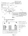
- FIG. 1illustrates an exemplary embodiment of an array of sensor cells
- FIG. 2illustrates an exemplary embodiment of a field effect transistor (FET) configured to sense a biomolecule
- FIG. 3illustrates a schematic diagram of an inverting gain amplifier circuit that includes the sensor FET
- FIG. 4depicts aspects of inverting gain characteristics of the inverting gain amplifier circuit
- FIG. 5depicts aspects of one sensor cell having a circuit configured to have low resistance in the components coupling output of the inverting gain amplifier circuit to a sensing line;
- FIG. 6depicts aspects of a circuit configured to turn off an FET in sensor cells 10 that are not selected for obtaining a measurement
- FIG. 7depicts aspects of a circuit having a p-type FET disposed in series with a source of a p-type FET in the inverting gain amplifier circuit and configured to de-energize the inverting gain amplifier circuit;
- FIG. 8depicts aspects of a circuit having an n-type FET disposed in series with a source of the sensor FET in the inverting gain amplifier circuit and configured to de-energize the inverting gain amplifier circuit;
- FIG. 9depicts aspects of an amplifying and decoupling circuit configured to decouple and amplify a measurement signal from the V SENSE line and also linearly amplifies the V X signal in the range of ⁇ V GN before the V X signal is transmitted to the V SENSE line.
- FIG. 10illustrates plots of output of the inverting gain amplifier versus gate voltage of the sensor FET
- FIGS. 11 and 12depict embodiments for interrupting a current path to the inverting gain amplifier
- FIG. 13illustrates movement of a biasing point of the gate voltage of the sensor FET corresponding to a change in the voltage thresholds of the sensor FET and another FET in the inverting gain amplifier circuit
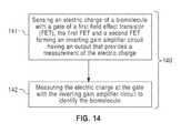
- FIG. 14presents one example of a method for identifying a biomolecule having an associated electric charge.
- the techniqueswhich include apparatus and method, call for using a field effect transistor (FET) as a sensor for sensing the biomolecule.
- FETfield effect transistor
- the techniquesprovide embodiments of circuits that automate the detection and, thus, identification of the biomolecule using the FET sensor.
- the techniquescall for fabricating an automated sensing platform using standard complementary metal-oxide-semiconductor (CMOS) technology.
- CMOScomplementary metal-oxide-semiconductor
- An array of sensor cellsis used to detect the biomolecule where each sensor cell includes at least one FET sensor and associated circuitry for amplifying a signal from the FET sensor.
- the signalsuch as a voltage reading, is used to detect the biomolecule.
- circuitrymay be provided to select a reading (i.e., signal) from a particular sensor cell and for conserving power.
- One sensor readingmay be used to confirm or validate a reading from another sensor cell.
- Another is that certain sensor cellsmay have FET sensors optimized for detecting a particular type of biomolecule.
- FIG. 1illustrates an exemplary embodiment of an array of sensor cells 10 .
- Each sensor cell 10is configured to sense a biomolecule and provide a signal such as a voltage reading that can be used to detect the biomolecule.
- the array of sensor cells 10 in the embodiment of FIG. 1is a matrix arrangement wherein each cell 10 is defined by a row number and a column number.
- a row select circuit 11is configured to select a row of cells 10 to be read by energizing each sensor cell 10 in the selected row.
- a column multiplexing circuit 12is configured to read a signal from one cell 10 in each column. Thus, by selecting a row, each cell 10 within the row will be read by the column multiplexing circuit 12 .
- V SENSEthe amplified signal or voltage reading for each cell 10 is referred to as V SENSE .
- V SENSEis sent to relatively long interconnect lines to be transferred outside of the array for further processing.
- V SENSEmay be amplified again outside of the sensor cell 10 and then converted to a digital signal via an analog to digital converter (ADC) 13 .
- ADCanalog to digital converter
- there can be less ADCsthere can be less ADCs. Using less ADCs requires selecting the V SENSE signals in an order using the column multiplexing circuit. This will take more time to perform the analog to digital conversion, but an advantage is that less area will be required on a semiconductor chip.
- FIG. 2illustrates an exemplary embodiment of an FET 20 configured to sense a biomolecule 21 .
- the FET 20 in the embodiment of FIG. 1is a finFET having a fin 22 covered with a gate dielectric 23 .
- One non-limiting embodiment of the gate dielectric 23is SiO 2 /HfO 2 .
- the gate dielectric 23is covered with a gate surface material 24 that is configured to adhere to the biomolecule 21 .
- the FET 20does not have a conventional top gate.
- An electrolyte 25surrounds the gate surface material 24 and acts as the top gate.
- the fin 22 and the gate dielectric 23are situated atop a buried oxide (BOX) layer 26 that is situated atop of a silicon layer 27 , which is the back gate of the FET 20 .
- BOXburied oxide
- the drain current of the FET 20is operated in the sub-threshold region.
- the biomolecule 21binds to the gate surface material 24 and transfers an electric charge to the gate dielectric 23 .
- the electric charge at the gate dielectric 23affects the drain current, which in turn affects the drain to source voltage of the FET 20 .
- the measured drain to source voltageis V SENSE .
- the measurement of V SENSEcan be used to identify the specific biomolecule 21 being detected.
- the advantage of using an FET 20 to sense the biomolecule 21is that the FET 20 has high sensitivity to the electric charge of the biomolecule 21 .
- the high sensitivityresults from a small sub-threshold slope such that a small change in the gate voltage causes a large change in the drain current resulting in a large change in the drain to source voltage (i.e., V SENSE ).
- the larger surface area of the gate dielectric 23 in finFETs compared to non-fin FETsresults in an improved response time.
- the finFET used as the FET 20can have a single fin or an array of fins to further increase the surface area of the gate dielectric 23 .
- FIG. 2illustrates a finFET
- other types of FETsmay also be used to detect the biomolecule 21 .
- the FET 20is generally implemented using complementary metal-oxide-semiconductor (CMOS) technology.
- CMOScomplementary metal-oxide-semiconductor
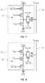
- FIG. 3illustrates a schematic diagram of an inverting gain amplifier circuit 30 .
- the inverting gain amplifier circuit 30includes the FET 20 as the sensor for sensing the biomolecule 21 .
- the FET 20is an n-type FET and is designated FET N1.
- the FET N1is coupled in series with a p-type FET, FET P1. That is, the drain of FET N1 is coupled to the drain of FET P1 and the source of FET P1 is coupled to a power supply designated V DD1 and supplying voltage V DD1 .
- the FET N1 and the FET P1form the inverting gain amplifier circuit 30 .
- V SENSEn-type FET
- FET N2transfers the output of the FET N1, V X , which is related to the detected electric charge of the biomolecule 21 , to a V SENSE line 31 .
- the voltage read at the V SENSE line 31is referred to as V SENSE .
- the V SENSE line 31is outside of the sensor cell 10 .
- the FET N2is configured to receive a “row select” signal (i.e., row_sel) from the row select circuit 11 such that when a gate of the FET N2 is energized (i.e., set to V DD1 ), then the output voltage, V X , is coupled to the V SENSE line 31 .
- FET N2is “ON”, then V SENSE becomes generally the same as V X .
- FIG. 4depicts aspects of inverting gain characteristics of the inverting gain amplifier circuit 30 .
- the output of the amplifier circuit 30is graphed versus the gate voltage, V GN , of FET N1.
- the sensing FET N1is biased to operate in the sub-threshold region, such that 0 ⁇ V GN ⁇ V T,N1 .
- the p-type FET P1is biased to operate such that V GP ⁇ V DD1 ⁇ V T,P1 , where V T,P1 is the threshold of the p-type FET P1.
- FIG. 5depicts aspects of the sensor cell 10 having a circuit configured to have low resistance in the components coupling V X to the V SENSE line.
- a p-type FET, FET N2is disposed in parallel to FET N2 such that the gate of FET N2 is coupled to the complement of the row select signal.
- FET N2is disposed in parallel to FET N2 such that the gate of FET N2 is coupled to the complement of the row select signal.
- This configurationwill transfer a wide range of values of V X to the V SENSE line. However, it is noted that this configuration will also increase leakage in the sensor cells 10 that are not selected for reading.
- FIG. 6depicts aspects of a circuit configured to turn off the FET P1 in the sensor cells 10 that are not selected for reading.
- the circuit in FIG. 3includes a p-type FET, FET P8, disposed between V DD1 and gates of all P1 FETs in a row of the array. Further, n-type FET N9 and p-type FET P9 are connected in parallel such that their drains are tied together and connected to V GP and their sources are connected to the gate of all P1 FETs in the row of the array.
- FET P8 and FET N9are connected to the row enable signal “row_sel.”
- the gate of FET P9is connected to the complement of the “row_sel” signal.
- This circuitis common to all sensor cells 10 in a row. All the sensor cells 10 in a row have a common V GP . In the sensor cells 10 that are unselected, the row select will be “0” and, hence, the FET P8 will be ON connecting gates of all P1 FETs in a row to V DD1 . Thus, in all the unselected sensor cells 10 , the FET P1 will be turned OFF to stop the current flowing in the path V DD1 to GND. In a selected row, FET P8 will be OFF and FET P9 and FET N9 will be ON so as to connect the gate of all P1 FETs in the row to V GP .
- FIG. 7depicts aspects of a circuit having a p-type FET, FET P3, disposed in series with the FET P1, i.e., between the power supply V DD1 and the source of the FET P1.
- the FET P3is turned OFF when a row is not selected, i.e., when the row select signal is low, thus, stopping the current flowing in the path V DD1 to GND.
- FIG. 8depicts aspects of a circuit having an n-type FET, FET N3, disposed in series with the FET N1, i.e., between the source of the FET N1 and the ground, GND.
- the FET N3is turned OFF when a row is not selected, i.e., when the row select signal is low, thus, stopping the current flowing in the path V DD1 to GND.
- several sensor cells 10may be connected to the common V SENSE line resulting in the V SENSE line being very long and, hence, having a relatively large resistance and capacitance.
- charging and/or discharging of a connection line connecting the V X signal to the V SENSE line through the FET N1 and the FET P1can contribute significant noise to the V X signal.
- the charging and/or dischargingcan cause an increase in the amount of time it takes to stabilize the V X signal transmitted to the V SENSE line.
- an amplifying and decoupling circuit disposed in the connection lineis disclosed.
- FIG. 9depicts aspects of an amplifying and decoupling circuit 90 that decouples the V X signal from the V SENSE line and also linearly amplifies the V X signal in the range of ⁇ V GN before the V X signal is transmitted to the V SENSE line.
- the amplifying and decoupling circuit 90includes n-type FETs, FET N4 and FET N5, and p-type FETs, FET P4 and FET P5.
- FETs N4, N5, P4 and P5are configured as shown in FIG. 9 between (1) a node at the inverting gain amplifier circuit 30 providing the V X signal and (2) the V SENSE line.
- FET N4 and FET P4are in an inverter configuration with the V X signal as input and V SENSE as output.
- FET N5 and FET P5are feedback transistors.
- multiple gate FETssuch as finFETS with independent backgate control may be used in lieu of the single gate FETs to make the amplifying and decoupling circuit 90 .
- FET N4 and FET N5can be substituted with a single multiple gate FET with FET N5 as a backgate.
- FET P4 and FET P5can be substituted with a single multiple gate FET with FET P5 as a backgate.
- the amplifying and decoupling circuit 90is coupled to a separate power supply V DD2 (having voltage V DD2 ) so as to achieve a desired voltage range for V SENSE .
- the inverting gain amplifier circuit 30is based on the change in V X due to a change in V GN .
- the change in V X due to a change in V GNcan be deterministically correlated when ⁇ V X / ⁇ V GN is a definite function in the given range of ⁇ V GN .
- FET N1 and FET P1form an inverting gain circuit, the gain is very high near the biasing point, i.e., at the chosen value of V GN as shown in FIG. 4 .
- Amplification of V GNis beneficial but the amplification can limit the range if values of ⁇ V GN due to saturation of V X for low or high values of V GN . It is preferable to have correlation between ⁇ V X and ⁇ V GN in the full range of values of ⁇ V GN .
- FIG. 10illustrates plots of V SENSE and V X versus V GN . It is noted that linearization circuitry results in a linear correlation between V SENSE and V GN for a wide range of ⁇ V GN from the biasing point.
- FIG. 10also shows a plot of V SENSE with and without the feedback FETs N5 and P5. Without feedback, the output of the inverting gain amplifier circuit 30 has very high amplification, thereby, having the potential for a large change in V SENSE for a little change in V GN . Thus, V SENSE can saturate for a large change in V GN . This potential for saturation limits the region of operation of V GN , hence, feedback is necessary for detecting the large change in V GN , due to detecting a large change in electric charge of the biomolecule 21 .
- FIG. 11depicts an embodiment for interrupting the current path by disposing a p-type FET, FET P6, between the power supply V DD2 and the sources of FETs P4 and P5.
- FIG. 12depicts another embodiment for interrupting the current path by disposing an n-type FET, FET N6, between the sources of FETs N4 and N5 and ground.
- the amplifying and decoupling circuit 90which may include the current interrupting circuitry, can be implemented in each sensor cell 10 or, alternatively, by sharing the circuit 90 with the sensor cells 10 in a column. In the sharing embodiment, the amplifying and decoupling circuit 90 is coupled between the V SENSE line and the column multiplexing circuit 12 shown in FIG. 1 to reduce the area needed by each sensor cell 10 .
- V0 SENSEis the analog voltage signal that is converted to a digital signal, which can be stored in a conventional semiconductor memory integrated onto the chip or connected externally.
- the stored digital value of V0 SENSE for each sensor cell 10will serve as reference point for future measurements performed by that sensor cell 10 .
- the measured digital value of V SENSEwill be in reference to original stored value of V0 SENSE .
- This calibration techniquedoes not require any changes in the hardware. Hence, the same hardware can be repeatedly used for different kinds of biomolecules 21 after quick calibration i.e., measurement of V0 SENSE .
- V GNSensor tuning to test a variety of the biomolecules 21 that may require different biasing points
- the range of operation of the sensing FET N1depends on the choice of biasing point V GN .
- the biological molecule 21should not experience any resistance due to V GN while binding to the gate of the FET N1. If different biomolecules 21 require different biasing points, i.e., V GN values, then the similar ⁇ V GN values can be determined. This can be achieved by dynamically controlling the threshold voltage V T of FETs N1 and P1.
- FIG. 13illustrates the movement of biasing point V GN with the change in V T of FETs N1 and P1.
- V T, N1, P1can be achieved by changing the substrate bias of FETs N1 and P1 (i.e., single gate FETs) with substrate contact.
- FETs N1 and P1i.e., single gate FETs
- V Tcan be dynamically modified by controlling the voltage bias at the back (or second) gate of these FETs.
- FIG. 14presents one example of a method 140 for identifying the biomolecule 21 having an associated electric charge.
- the method 140calls for (step 141 ) sensing the electric charge of the biomolecule 21 with the gate dielectric 23 of the FET 20 .
- the FET 20 and another FETare configured to form the inverting gain amplifier circuit 30 .
- the method 140calls for (step 142 ) measuring the electric charge at the gate with the inverting gain amplifier circuit to identify the biomolecule 21 .
- any material having an electric charge that may adhere to the gate dielectric 23can be identified.
- testing and/or analysis of different biomolecules 21 and materials having differing electric chargesare used to determine a reference electric charge associated with each test biomolecule 21 /material.
- the biomolecule 21 /materialcan be identified.
- the array of sensors 10can be built into one CMOS device or semiconductor “chip” to lower production cost and improve reliability.
- other components used with the array of sensors 10such as the row select circuit 11 , the column multiplexing circuit 12 and the ADC 13 , can also be built into the same CMOS device.
- the capabilities of the present inventioncan be implemented in software, firmware, hardware or some combination thereof.
- one or more aspects of the present inventioncan be included in an article of manufacture (e.g., one or more computer program products) having, for instance, computer usable media.
- the mediahas embodied therein, for instance, computer readable program code means for providing and facilitating the capabilities of the present invention.
- the article of manufacturecan be included as a part of a computer system or sold separately.
- At least one program storage devicereadable by a machine, tangibly embodying at least one program of instructions executable by the machine to perform the capabilities of the present invention can be provided.
- various analysis componentsmay be used, including a digital and/or an analog system.
- the systemmay have components such as a processor, storage media, memory, input, output, communications link, user interfaces (such as a printer or a display), software programs, signal processors (digital or analog) and other such components (such as resistors, capacitors, inductors and others) to provide for operation and analyses of the apparatus and methods disclosed herein in any of several manners well-appreciated in the art.
- teachingsmay be, but need not be, implemented in conjunction with a set of computer executable instructions stored on a computer readable medium, including memory (ROMs, RAMs), optical (CD-ROMs), or magnetic (disks, hard drives), or any other type that when executed causes a computer to implement the method of the present invention.
- ROMs, RAMsrandom access memory
- CD-ROMscompact disc-read only memory
- magnetic (disks, hard drives)any other type that when executed causes a computer to implement the method of the present invention.
- These instructionsmay provide for equipment operation, control, data collection and analysis and other functions deemed relevant by a system designer, owner, user or other such personnel, in addition to the functions described in this disclosure.
Landscapes
- Health & Medical Sciences (AREA)
- Life Sciences & Earth Sciences (AREA)
- Chemical & Material Sciences (AREA)
- Engineering & Computer Science (AREA)
- Physics & Mathematics (AREA)
- Molecular Biology (AREA)
- Analytical Chemistry (AREA)
- Microelectronics & Electronic Packaging (AREA)
- Spectroscopy & Molecular Physics (AREA)
- Chemical Kinetics & Catalysis (AREA)
- Electrochemistry (AREA)
- Power Engineering (AREA)
- Biochemistry (AREA)
- General Health & Medical Sciences (AREA)
- General Physics & Mathematics (AREA)
- Immunology (AREA)
- Pathology (AREA)
- Investigating Or Analyzing Materials By The Use Of Electric Means (AREA)
- Apparatus Associated With Microorganisms And Enzymes (AREA)
Abstract
Description
Claims (15)
Priority Applications (7)
| Application Number | Priority Date | Filing Date | Title |
|---|---|---|---|
| US12/651,504US8052931B2 (en) | 2010-01-04 | 2010-01-04 | Ultra low-power CMOS based bio-sensor circuit |
| CA2786285ACA2786285A1 (en) | 2010-01-04 | 2011-01-03 | Ultra low-power cmos based bio-sensor circuit |
| PCT/US2011/020007WO2011082395A1 (en) | 2010-01-04 | 2011-01-03 | Ultra low-power cmos based bio-sensor circuit |
| JP2012547326AJP5663036B2 (en) | 2010-01-04 | 2011-01-03 | Ultra-low power CMOS-based biosensor circuit |
| CN201180005322.XACN102695952B (en) | 2010-01-04 | 2011-01-03 | Biosensor circuit based on ultra-low power CMOS |
| EP11728544.5AEP2521909B1 (en) | 2010-01-04 | 2011-01-03 | Ultra low-power cmos based bio-sensor circuit |
| US13/232,395US8409867B2 (en) | 2010-01-04 | 2011-09-14 | Ultra low-power CMOS based bio-sensor circuit |
Applications Claiming Priority (1)
| Application Number | Priority Date | Filing Date | Title |
|---|---|---|---|
| US12/651,504US8052931B2 (en) | 2010-01-04 | 2010-01-04 | Ultra low-power CMOS based bio-sensor circuit |
Related Child Applications (1)
| Application Number | Title | Priority Date | Filing Date |
|---|---|---|---|
| US13/232,395DivisionUS8409867B2 (en) | 2010-01-04 | 2011-09-14 | Ultra low-power CMOS based bio-sensor circuit |
Publications (2)
| Publication Number | Publication Date |
|---|---|
| US20110163812A1 US20110163812A1 (en) | 2011-07-07 |
| US8052931B2true US8052931B2 (en) | 2011-11-08 |
Family
ID=44224375
Family Applications (2)
| Application Number | Title | Priority Date | Filing Date |
|---|---|---|---|
| US12/651,504ActiveUS8052931B2 (en) | 2010-01-04 | 2010-01-04 | Ultra low-power CMOS based bio-sensor circuit |
| US13/232,395Expired - Fee RelatedUS8409867B2 (en) | 2010-01-04 | 2011-09-14 | Ultra low-power CMOS based bio-sensor circuit |
Family Applications After (1)
| Application Number | Title | Priority Date | Filing Date |
|---|---|---|---|
| US13/232,395Expired - Fee RelatedUS8409867B2 (en) | 2010-01-04 | 2011-09-14 | Ultra low-power CMOS based bio-sensor circuit |
Country Status (6)
| Country | Link |
|---|---|
| US (2) | US8052931B2 (en) |
| EP (1) | EP2521909B1 (en) |
| JP (1) | JP5663036B2 (en) |
| CN (1) | CN102695952B (en) |
| CA (1) | CA2786285A1 (en) |
| WO (1) | WO2011082395A1 (en) |
Cited By (2)
| Publication number | Priority date | Publication date | Assignee | Title |
|---|---|---|---|---|
| US9612224B2 (en) | 2015-05-29 | 2017-04-04 | International Business Machines Corporation | High density nano-array for sensing |
| US10908120B2 (en) | 2014-08-07 | 2021-02-02 | Laurus Corporation | Semiconductor biosensor and control method thereof |
Families Citing this family (12)
| Publication number | Priority date | Publication date | Assignee | Title |
|---|---|---|---|---|
| KR101101512B1 (en)* | 2010-07-29 | 2012-01-03 | 삼성전기주식회사 | CMOS power amplifier |
| US8994077B2 (en)* | 2012-12-21 | 2015-03-31 | International Business Machines Corporation | Field effect transistor-based bio sensor |
| US9806299B2 (en) | 2014-04-08 | 2017-10-31 | International Business Machines Corporation | Cathode for thin film microbattery |
| US10018660B2 (en) | 2014-06-12 | 2018-07-10 | Taiwan Semiconductor Manufacturing Company, Ltd. | Output resistance testing structure |
| JP6434744B2 (en)* | 2014-08-07 | 2018-12-05 | ローラス株式会社 | Semiconductor biosensor |
| US9508566B2 (en) | 2014-08-15 | 2016-11-29 | International Business Machines Corporation | Wafer level overmold for three dimensional surfaces |
| US10105082B2 (en) | 2014-08-15 | 2018-10-23 | International Business Machines Corporation | Metal-oxide-semiconductor capacitor based sensor |
| US12050196B2 (en)* | 2015-04-13 | 2024-07-30 | Life Technologies Corporation | Apparatuses, methods, systems, and computer-readable media for fluid potential artifact correction in reagent delivery systems |
| EP3848053A1 (en)* | 2015-12-11 | 2021-07-14 | Universität Bern | Inositol derivatives for use in pathological crystallization |
| US11092567B2 (en) | 2017-03-21 | 2021-08-17 | International Business Machines Corporation | Biosensor electrode having three-dimensional structured sensing surfaces |
| JP6644336B2 (en)* | 2018-08-06 | 2020-02-12 | シャープ株式会社 | Ion concentration sensor |
| LU101020B1 (en)* | 2018-11-28 | 2020-05-28 | Luxembourg Inst Science & Tech List | Ion-sensitive field effect transistor |
Citations (24)
| Publication number | Priority date | Publication date | Assignee | Title |
|---|---|---|---|---|
| US3562553A (en)* | 1968-10-21 | 1971-02-09 | Allen R Roth | Multiplier circuit |
| US4238757A (en) | 1976-03-19 | 1980-12-09 | General Electric Company | Field effect transistor for detection of biological reactions |
| US4657658A (en) | 1984-11-07 | 1987-04-14 | Alastair Sibbald | Semiconductor devices |
| US4984045A (en) | 1987-07-13 | 1991-01-08 | Kabushiki Kaisha Toshiba | Output sensor of charge transfer device |
| US5160597A (en) | 1989-04-21 | 1992-11-03 | Eniricerche S.P.A. | Sensor with antigen chemically bonded to a semiconductor device |
| US6258606B1 (en) | 1996-07-09 | 2001-07-10 | Nanogen, Inc. | Multiplexed active biologic array |
| DE10254158A1 (en) | 2002-11-20 | 2004-06-09 | Infineon Technologies Ag | Sensor system for detecting signals from biological cells comprises semiconductor substrate containing field effect transistor whose channel has coupling component connecting it to sensor surface |
| US20040109075A1 (en) | 2002-11-29 | 2004-06-10 | Nec Electronics Corporation | CCD image sensor |
| US20040256655A1 (en) | 2002-10-29 | 2004-12-23 | Edwin Kan | Chemoreceptive semiconductor structure |
| US20050068015A1 (en) | 2003-09-29 | 2005-03-31 | Intel Corporation | Regulated sleep transistor apparatus, method, and system |
| US7019305B2 (en) | 2001-10-16 | 2006-03-28 | Infineon Technologies Ag | Biosensor circuit and sensor array consisting of a plurality of said biosensor circuits and biosensor array |
| US20060145194A1 (en) | 2002-11-19 | 2006-07-06 | William Marsh Rice University | Method for creating a functional interface between a nanoparticle, nanotube or nanowire, and a biological molecule or system |
| US20060272942A1 (en) | 2003-03-18 | 2006-12-07 | Henning Sirringhaus | Electrochemical microfluidic sensor and method of creation of its microchannels by embossing |
| US7151301B2 (en) | 2004-02-20 | 2006-12-19 | Samsung Electronics Co., Ltd. | Sensitivity enhanced biomolecule field effect transistor |
| US20070159216A1 (en) | 2006-01-09 | 2007-07-12 | Samsung Electronics Co., Ltd., | Fet-based sensor for detecting ionic material, ionic material detecting device using the fet-based sensor, and method of detecting ionic material using the fet-based sensor |
| US20070252176A1 (en) | 2006-04-26 | 2007-11-01 | Samsung Electronics Co., Ltd., | Field effect transistor for detecting ionic material and method of detecting ionic material using the same |
| US7291496B2 (en) | 2003-05-22 | 2007-11-06 | University Of Hawaii | Ultrasensitive biochemical sensor |
| US7317216B2 (en) | 2003-10-31 | 2008-01-08 | University Of Hawaii | Ultrasensitive biochemical sensing platform |
| US20080035494A1 (en) | 2006-03-17 | 2008-02-14 | Gomez Romel D R | Apparatus for microarray binding sensors having biological probe materials using carbon nanotube transistors |
| US7357018B2 (en) | 2006-02-10 | 2008-04-15 | Agilent Technologies, Inc. | Method for performing a measurement inside a specimen using an insertable nanoscale FET probe |
| WO2008068719A1 (en) | 2006-12-08 | 2008-06-12 | Koninklijke Philips Electronics N.V. | Method of manufacturing a semiconductor sensor device and semiconductor sensor device obtained with such method |
| US20080315861A1 (en) | 2007-06-19 | 2008-12-25 | Samsung Electronics Co., Ltd. | Biomolecule detector based on field effect transistor arrays containing reference electrodes and detection method for biomolecules using the same |
| US7507675B2 (en) | 2003-06-25 | 2009-03-24 | Asml Netherlands B.V. | Device manufacturing method and device |
| US20090127589A1 (en) | 2006-12-14 | 2009-05-21 | Ion Torrent Systems Incorporated | Methods and apparatus for measuring analytes using large scale FET arrays |
Family Cites Families (31)
| Publication number | Priority date | Publication date | Assignee | Title |
|---|---|---|---|---|
| JPS5013068B1 (en) | 1970-07-31 | 1975-05-16 | ||
| US4173818A (en) | 1978-05-30 | 1979-11-13 | International Business Machines Corporation | Method for fabricating transistor structures having very short effective channels |
| KR930002824B1 (en) | 1990-08-21 | 1993-04-10 | 손병기 | Measuring circuit for biosensor using deionized field effect transistor |
| JPH05312778A (en)* | 1992-05-14 | 1993-11-22 | Fuji Electric Co Ltd | Ion concentration sensor |
| JPH06249825A (en)* | 1993-02-26 | 1994-09-09 | Tokyo Gas Co Ltd | FET sensor |
| DE10133363A1 (en)* | 2001-07-10 | 2003-01-30 | Infineon Technologies Ag | Measuring cell and measuring field with such measuring cells as well as using a measuring cell and using a measuring field |
| JP3688611B2 (en)* | 2001-09-10 | 2005-08-31 | 株式会社東芝 | Sensor array |
| US6700151B2 (en) | 2001-10-17 | 2004-03-02 | Kilopass Technologies, Inc. | Reprogrammable non-volatile memory using a breakdown phenomena in an ultra-thin dielectric |
| DE10163557B4 (en) | 2001-12-21 | 2007-12-06 | Forschungszentrum Jülich GmbH | Transistor-based sensor with specially designed gate electrode for high-sensitivity detection of analytes |
| EP1348951A1 (en) | 2002-03-29 | 2003-10-01 | Interuniversitair Micro-Elektronica Centrum | Molecularly controlled dual gated field effect transistor for sensing applications |
| US20040110277A1 (en)* | 2002-04-12 | 2004-06-10 | Seiko Epson Corporation | Sensor cell, bio-sensor, capacitance element manufacturing method, biological reaction detection method and genetic analytical method |
| JP4832759B2 (en) | 2002-12-11 | 2011-12-07 | サントル ナショナル ドゥ ラ ルシェルシュ シアンティフィク | Method for electronically detecting at least one specific interaction between a probe molecule and a target biomolecule |
| DE10352917A1 (en) | 2003-11-11 | 2005-06-16 | Endress + Hauser Conducta Gesellschaft für Mess- und Regeltechnik mbH + Co. KG | Sensor arrangement with several potentiometric sensors |
| US7462512B2 (en) | 2004-01-12 | 2008-12-09 | Polytechnic University | Floating gate field effect transistors for chemical and/or biological sensing |
| DE102004019639A1 (en) | 2004-04-22 | 2005-11-17 | Siemens Ag | FET-based gas sensor |
| DE102004023855B4 (en)* | 2004-05-13 | 2006-11-30 | Infineon Technologies Ag | Circuit arrangement |
| GB2416210B (en)* | 2004-07-13 | 2008-02-20 | Christofer Toumazou | Ion sensitive field effect transistors |
| WO2006025180A1 (en)* | 2004-08-30 | 2006-03-09 | Japan Science And Technology Agency | Dna sensor |
| EP1810015A1 (en)* | 2004-10-14 | 2007-07-25 | Kabushiki Kaisha Toshiba | Fet-based nucleic acid detecting sensor |
| DE102004055929B4 (en) | 2004-11-19 | 2014-05-22 | Qimonda Ag | Non-volatile memory cell arrangement |
| US7132324B2 (en) | 2004-12-09 | 2006-11-07 | International Business Machines Corporation | SOI device with different crystallographic orientations |
| US7116113B1 (en) | 2005-05-04 | 2006-10-03 | Texas Instruments Incorporated | Systems and methods for sense FET calibration |
| JP2007088322A (en) | 2005-09-26 | 2007-04-05 | Matsushita Electric Ind Co Ltd | Semiconductor device and manufacturing method thereof |
| EP1982167A4 (en) | 2006-01-20 | 2010-06-30 | Agency Science Tech & Res | BIOSENSOR |
| US8129978B2 (en)* | 2006-07-13 | 2012-03-06 | National University Corporation Nagoya University | Material detector |
| US20080303095A1 (en) | 2007-06-07 | 2008-12-11 | Weize Xiong | Varying mugfet width to adjust device characteristics |
| US20100221846A1 (en)* | 2007-10-12 | 2010-09-02 | Nxp B.V. | Sensor, a sensor array, and a method of operating a sensor |
| JP5535950B2 (en)* | 2008-03-12 | 2014-07-02 | ザ トラスティーズ オブ ザ ユニバーシティ オブ ペンシルバニア | A flexible and expandable sensor array for recording and modulating physiological activity |
| JP2011525990A (en)* | 2008-06-26 | 2011-09-29 | ライフ テクノロジーズ コーポレーション | Method and apparatus for detecting molecular interactions using FET arrays |
| US7851790B2 (en) | 2008-12-30 | 2010-12-14 | Intel Corporation | Isolated Germanium nanowire on Silicon fin |
| US9029132B2 (en) | 2009-08-06 | 2015-05-12 | International Business Machines Corporation | Sensor for biomolecules |
- 2010
- 2010-01-04USUS12/651,504patent/US8052931B2/enactiveActive
- 2011
- 2011-01-03CACA2786285Apatent/CA2786285A1/ennot_activeAbandoned
- 2011-01-03WOPCT/US2011/020007patent/WO2011082395A1/enactiveApplication Filing
- 2011-01-03EPEP11728544.5Apatent/EP2521909B1/enactiveActive
- 2011-01-03CNCN201180005322.XApatent/CN102695952B/ennot_activeExpired - Fee Related
- 2011-01-03JPJP2012547326Apatent/JP5663036B2/ennot_activeExpired - Fee Related
- 2011-09-14USUS13/232,395patent/US8409867B2/ennot_activeExpired - Fee Related
Patent Citations (26)
| Publication number | Priority date | Publication date | Assignee | Title |
|---|---|---|---|---|
| US3562553A (en)* | 1968-10-21 | 1971-02-09 | Allen R Roth | Multiplier circuit |
| US4238757A (en) | 1976-03-19 | 1980-12-09 | General Electric Company | Field effect transistor for detection of biological reactions |
| US4657658A (en) | 1984-11-07 | 1987-04-14 | Alastair Sibbald | Semiconductor devices |
| US4984045A (en) | 1987-07-13 | 1991-01-08 | Kabushiki Kaisha Toshiba | Output sensor of charge transfer device |
| US5160597A (en) | 1989-04-21 | 1992-11-03 | Eniricerche S.P.A. | Sensor with antigen chemically bonded to a semiconductor device |
| US6258606B1 (en) | 1996-07-09 | 2001-07-10 | Nanogen, Inc. | Multiplexed active biologic array |
| US6682936B2 (en) | 1996-07-09 | 2004-01-27 | Nanogen, Inc. | Addressable biologic electrode array |
| US7150997B2 (en) | 1996-07-09 | 2006-12-19 | Nanogen, Inc. | Multiplexed active biologic array |
| US7019305B2 (en) | 2001-10-16 | 2006-03-28 | Infineon Technologies Ag | Biosensor circuit and sensor array consisting of a plurality of said biosensor circuits and biosensor array |
| US20040256655A1 (en) | 2002-10-29 | 2004-12-23 | Edwin Kan | Chemoreceptive semiconductor structure |
| US20060145194A1 (en) | 2002-11-19 | 2006-07-06 | William Marsh Rice University | Method for creating a functional interface between a nanoparticle, nanotube or nanowire, and a biological molecule or system |
| DE10254158A1 (en) | 2002-11-20 | 2004-06-09 | Infineon Technologies Ag | Sensor system for detecting signals from biological cells comprises semiconductor substrate containing field effect transistor whose channel has coupling component connecting it to sensor surface |
| US20040109075A1 (en) | 2002-11-29 | 2004-06-10 | Nec Electronics Corporation | CCD image sensor |
| US20060272942A1 (en) | 2003-03-18 | 2006-12-07 | Henning Sirringhaus | Electrochemical microfluidic sensor and method of creation of its microchannels by embossing |
| US7291496B2 (en) | 2003-05-22 | 2007-11-06 | University Of Hawaii | Ultrasensitive biochemical sensor |
| US7507675B2 (en) | 2003-06-25 | 2009-03-24 | Asml Netherlands B.V. | Device manufacturing method and device |
| US20050068015A1 (en) | 2003-09-29 | 2005-03-31 | Intel Corporation | Regulated sleep transistor apparatus, method, and system |
| US7317216B2 (en) | 2003-10-31 | 2008-01-08 | University Of Hawaii | Ultrasensitive biochemical sensing platform |
| US7151301B2 (en) | 2004-02-20 | 2006-12-19 | Samsung Electronics Co., Ltd. | Sensitivity enhanced biomolecule field effect transistor |
| US20070159216A1 (en) | 2006-01-09 | 2007-07-12 | Samsung Electronics Co., Ltd., | Fet-based sensor for detecting ionic material, ionic material detecting device using the fet-based sensor, and method of detecting ionic material using the fet-based sensor |
| US7357018B2 (en) | 2006-02-10 | 2008-04-15 | Agilent Technologies, Inc. | Method for performing a measurement inside a specimen using an insertable nanoscale FET probe |
| US20080035494A1 (en) | 2006-03-17 | 2008-02-14 | Gomez Romel D R | Apparatus for microarray binding sensors having biological probe materials using carbon nanotube transistors |
| US20070252176A1 (en) | 2006-04-26 | 2007-11-01 | Samsung Electronics Co., Ltd., | Field effect transistor for detecting ionic material and method of detecting ionic material using the same |
| WO2008068719A1 (en) | 2006-12-08 | 2008-06-12 | Koninklijke Philips Electronics N.V. | Method of manufacturing a semiconductor sensor device and semiconductor sensor device obtained with such method |
| US20090127589A1 (en) | 2006-12-14 | 2009-05-21 | Ion Torrent Systems Incorporated | Methods and apparatus for measuring analytes using large scale FET arrays |
| US20080315861A1 (en) | 2007-06-19 | 2008-12-25 | Samsung Electronics Co., Ltd. | Biomolecule detector based on field effect transistor arrays containing reference electrodes and detection method for biomolecules using the same |
Non-Patent Citations (8)
| Title |
|---|
| F. Patolsky et al., Electrical detection of single viruses, PNAS, Sep. 28, 2004, pp. 14017-14022, vol. 101, No. 39, PNAS. |
| H. Im et al., A dielectric-modulated field-effect transistor for biosensing, Nature Nanotechnology, Jul. 2007, pp. 430-434, vol. 2, Nature Publishing Group. |
| Han, Label-free detection of biomlecules by a field-effect transistor microarray biosensor with bio-functionalized gate surfaces, Dec. 2006 [retrieved on Mar. 17, 2011]. Retrieved from the internet:,URL: http://juwel.fz-juelich.de:8080/dspace/bitstream/2128/2597/1/Juel-4227-Han.pdf. |
| Huang, et al. "Development of Active Matrix Biosensor Array for Cell Screening". Proc. of IEEE Sensors 2004. |
| K. Nakazato, et al. "CMOS Cascode Source-Drain Follower for Monolithically Integrated Biosensor Array". IEICE Trans. Electron., vol. E91-C, No. 9 Sep. 2008. pp. 1505-1515. |
| Lee, et al., Ion-Sensitive Field-Effect Transistor for Biological Sensing, Sensors 2003, 9, 7111-7131; doi:10.3390/s90907111 [online], Sep. 7, 2009 [retrieved on Mar. 17, 2011]. Retrieved from the Internet:, URL:http://www.mdpi.com/1424-8220/9/7111/pdf. |
| Maher, Electrical Engineering 234 Electrical Engineering Circuit Laboratory, Manual [online], Jun. 1992 [retrieved on Mar. 17, 2011]. Retrieved from the Internet:,URL:http://www.coe.montana.edu/ee/rmaher/teaching/EEngr-234-Labs-maher.pdf>p. 8-1 to 8-20. |
| Notification of Transmittal of the International Search Report and the Written Opinion of the International Searching Authority, or the Declaration; PCT/US11/20007;Apr. 6, 2011. |
Cited By (4)
| Publication number | Priority date | Publication date | Assignee | Title |
|---|---|---|---|---|
| US10908120B2 (en) | 2014-08-07 | 2021-02-02 | Laurus Corporation | Semiconductor biosensor and control method thereof |
| US9612224B2 (en) | 2015-05-29 | 2017-04-04 | International Business Machines Corporation | High density nano-array for sensing |
| US9753006B2 (en) | 2015-05-29 | 2017-09-05 | International Business Machines Corporation | High density nano-array for sensing |
| US10620158B2 (en) | 2015-05-29 | 2020-04-14 | International Business Machines Corporation | High density nano-array for sensing |
Also Published As
| Publication number | Publication date |
|---|---|
| US8409867B2 (en) | 2013-04-02 |
| EP2521909A4 (en) | 2017-07-26 |
| US20120001614A1 (en) | 2012-01-05 |
| EP2521909A1 (en) | 2012-11-14 |
| CN102695952A (en) | 2012-09-26 |
| EP2521909B1 (en) | 2018-11-07 |
| WO2011082395A1 (en) | 2011-07-07 |
| US20110163812A1 (en) | 2011-07-07 |
| CA2786285A1 (en) | 2011-07-07 |
| CN102695952B (en) | 2014-07-23 |
| JP2013516613A (en) | 2013-05-13 |
| JP5663036B2 (en) | 2015-02-04 |
Similar Documents
| Publication | Publication Date | Title |
|---|---|---|
| US8052931B2 (en) | Ultra low-power CMOS based bio-sensor circuit | |
| JP5890423B2 (en) | ISFET device | |
| JP6275184B2 (en) | Matched pair transistor circuit | |
| JP4801064B2 (en) | Signal processing circuit including ion sensitive field effect transistors and method for monitoring fluid properties | |
| US20060057025A1 (en) | Sensor arrangement and method for operating a sensor arrangement | |
| JP2016188867A (en) | Methods and apparatus for testing isfet arrays | |
| US20100007326A1 (en) | Material Detector | |
| JP2006138846A (en) | Nucleic acid detection sensor, nucleic acid detection chip and nucleic acid detection apparatus | |
| US8368454B2 (en) | Temperature detection circuit | |
| CN103376284A (en) | Multi-parameter low-power-consumption current-mode ion sensitive field effect tube array sensor device | |
| US10488365B2 (en) | Current sensors using bipolar transistors | |
| US20120327972A1 (en) | Temperature sensor | |
| US20170234816A1 (en) | Temperature sensor based on direct threshold-voltage sensing for on-chip dense thermal monitoring | |
| CN100446417C (en) | Integrated ISFET Sensor Signal Differential Readout Circuit Based on Dual Mode | |
| Nakazato et al. | CMOS cascode source-drain follower for monolithically integrated biosensor array | |
| Kalofonou et al. | An ISFET based chemical gilbert cell | |
| CN104677967A (en) | Ion sensitive field effect transistor sensor and voltage mode reading circuit thereof | |
| CN104407373B (en) | radiation detection circuit | |
| JP5265834B2 (en) | Amplifying device for sensor and physical quantity measuring system using this device | |
| Park et al. | Toxin detection by Si photosensitive biosensors with a new measurement scheme | |
| CN103534598B (en) | Analysis circuit for field effect transistors having a displaceable gate structure | |
| Yadav | Basudha Dewan, Ashwini Kumar, Shalini Chaudhary, and | |
| Lee et al. | Design and fabrication of CMOS micro humidity sensor system | |
| Do et al. | An improved inverter-based readout scheme for low | |
| CN104345328A (en) | Radiation detection circuit |
Legal Events
| Date | Code | Title | Description |
|---|---|---|---|
| AS | Assignment | Owner name:INTERNATIONAL BUSINESS MACHINES CORPORATION, NEW Y Free format text:ASSIGNMENT OF ASSIGNORS INTEREST;ASSIGNORS:BANSAL, ADITYA;ZAFAR, SUFI;REEL/FRAME:023726/0660 Effective date:20091104 | |
| STCF | Information on status: patent grant | Free format text:PATENTED CASE | |
| FPAY | Fee payment | Year of fee payment:4 | |
| AS | Assignment | Owner name:GLOBALFOUNDRIES U.S. 2 LLC, NEW YORK Free format text:ASSIGNMENT OF ASSIGNORS INTEREST;ASSIGNOR:INTERNATIONAL BUSINESS MACHINES CORPORATION;REEL/FRAME:036550/0001 Effective date:20150629 | |
| AS | Assignment | Owner name:GLOBALFOUNDRIES INC., CAYMAN ISLANDS Free format text:ASSIGNMENT OF ASSIGNORS INTEREST;ASSIGNORS:GLOBALFOUNDRIES U.S. 2 LLC;GLOBALFOUNDRIES U.S. INC.;REEL/FRAME:036779/0001 Effective date:20150910 | |
| AS | Assignment | Owner name:WILMINGTON TRUST, NATIONAL ASSOCIATION, DELAWARE Free format text:SECURITY AGREEMENT;ASSIGNOR:GLOBALFOUNDRIES INC.;REEL/FRAME:049490/0001 Effective date:20181127 | |
| MAFP | Maintenance fee payment | Free format text:PAYMENT OF MAINTENANCE FEE, 8TH YEAR, LARGE ENTITY (ORIGINAL EVENT CODE: M1552); ENTITY STATUS OF PATENT OWNER: LARGE ENTITY Year of fee payment:8 | |
| AS | Assignment | Owner name:GLOBALFOUNDRIES U.S. INC., CALIFORNIA Free format text:ASSIGNMENT OF ASSIGNORS INTEREST;ASSIGNOR:GLOBALFOUNDRIES INC.;REEL/FRAME:054633/0001 Effective date:20201022 | |
| AS | Assignment | Owner name:GLOBALFOUNDRIES INC., CAYMAN ISLANDS Free format text:RELEASE BY SECURED PARTY;ASSIGNOR:WILMINGTON TRUST, NATIONAL ASSOCIATION;REEL/FRAME:054636/0001 Effective date:20201117 | |
| AS | Assignment | Owner name:GLOBALFOUNDRIES U.S. INC., NEW YORK Free format text:RELEASE BY SECURED PARTY;ASSIGNOR:WILMINGTON TRUST, NATIONAL ASSOCIATION;REEL/FRAME:056987/0001 Effective date:20201117 | |
| MAFP | Maintenance fee payment | Free format text:PAYMENT OF MAINTENANCE FEE, 12TH YEAR, LARGE ENTITY (ORIGINAL EVENT CODE: M1553); ENTITY STATUS OF PATENT OWNER: LARGE ENTITY Year of fee payment:12 |