US8051799B2 - Object-processing apparatus controlling production of particles in electric field or magnetic field - Google Patents
Object-processing apparatus controlling production of particles in electric field or magnetic fieldDownload PDFInfo
- Publication number
- US8051799B2 US8051799B2US11/769,919US76991907AUS8051799B2US 8051799 B2US8051799 B2US 8051799B2US 76991907 AUS76991907 AUS 76991907AUS 8051799 B2US8051799 B2US 8051799B2
- Authority
- US
- United States
- Prior art keywords
- dielectric
- value
- deposit
- magnetic
- set forth
- Prior art date
- Legal status (The legal status is an assumption and is not a legal conclusion. Google has not performed a legal analysis and makes no representation as to the accuracy of the status listed.)
- Expired - Fee Related, expires
Links
Images


Classifications
- C—CHEMISTRY; METALLURGY
- C23—COATING METALLIC MATERIAL; COATING MATERIAL WITH METALLIC MATERIAL; CHEMICAL SURFACE TREATMENT; DIFFUSION TREATMENT OF METALLIC MATERIAL; COATING BY VACUUM EVAPORATION, BY SPUTTERING, BY ION IMPLANTATION OR BY CHEMICAL VAPOUR DEPOSITION, IN GENERAL; INHIBITING CORROSION OF METALLIC MATERIAL OR INCRUSTATION IN GENERAL
- C23C—COATING METALLIC MATERIAL; COATING MATERIAL WITH METALLIC MATERIAL; SURFACE TREATMENT OF METALLIC MATERIAL BY DIFFUSION INTO THE SURFACE, BY CHEMICAL CONVERSION OR SUBSTITUTION; COATING BY VACUUM EVAPORATION, BY SPUTTERING, BY ION IMPLANTATION OR BY CHEMICAL VAPOUR DEPOSITION, IN GENERAL
- C23C16/00—Chemical coating by decomposition of gaseous compounds, without leaving reaction products of surface material in the coating, i.e. chemical vapour deposition [CVD] processes
- C23C16/44—Chemical coating by decomposition of gaseous compounds, without leaving reaction products of surface material in the coating, i.e. chemical vapour deposition [CVD] processes characterised by the method of coating
- C23C16/4401—Means for minimising impurities, e.g. dust, moisture or residual gas, in the reaction chamber
- C23C16/4404—Coatings or surface treatment on the inside of the reaction chamber or on parts thereof
- H—ELECTRICITY
- H01—ELECTRIC ELEMENTS
- H01J—ELECTRIC DISCHARGE TUBES OR DISCHARGE LAMPS
- H01J37/00—Discharge tubes with provision for introducing objects or material to be exposed to the discharge, e.g. for the purpose of examination or processing thereof
- H01J37/02—Details
- H01J37/04—Arrangements of electrodes and associated parts for generating or controlling the discharge, e.g. electron-optical arrangement or ion-optical arrangement
- H01J37/09—Diaphragms; Shields associated with electron or ion-optical arrangements; Compensation of disturbing fields
- H—ELECTRICITY
- H01—ELECTRIC ELEMENTS
- H01J—ELECTRIC DISCHARGE TUBES OR DISCHARGE LAMPS
- H01J37/00—Discharge tubes with provision for introducing objects or material to be exposed to the discharge, e.g. for the purpose of examination or processing thereof
- H01J37/02—Details
- H01J37/16—Vessels; Containers
- H—ELECTRICITY
- H01—ELECTRIC ELEMENTS
- H01J—ELECTRIC DISCHARGE TUBES OR DISCHARGE LAMPS
- H01J37/00—Discharge tubes with provision for introducing objects or material to be exposed to the discharge, e.g. for the purpose of examination or processing thereof
- H01J37/32—Gas-filled discharge tubes
- H01J37/32431—Constructional details of the reactor
- H01J37/32458—Vessel
- H01J37/32467—Material
- H—ELECTRICITY
- H01—ELECTRIC ELEMENTS
- H01J—ELECTRIC DISCHARGE TUBES OR DISCHARGE LAMPS
- H01J37/00—Discharge tubes with provision for introducing objects or material to be exposed to the discharge, e.g. for the purpose of examination or processing thereof
- H01J37/32—Gas-filled discharge tubes
- H01J37/32431—Constructional details of the reactor
- H01J37/32458—Vessel
- H01J37/32477—Vessel characterised by the means for protecting vessels or internal parts, e.g. coatings
- H—ELECTRICITY
- H01—ELECTRIC ELEMENTS
- H01J—ELECTRIC DISCHARGE TUBES OR DISCHARGE LAMPS
- H01J2237/00—Discharge tubes exposing object to beam, e.g. for analysis treatment, etching, imaging
- H01J2237/02—Details
- H01J2237/022—Avoiding or removing foreign or contaminating particles, debris or deposits on sample or tube
- H—ELECTRICITY
- H01—ELECTRIC ELEMENTS
- H01J—ELECTRIC DISCHARGE TUBES OR DISCHARGE LAMPS
- H01J2237/00—Discharge tubes exposing object to beam, e.g. for analysis treatment, etching, imaging
- H01J2237/02—Details
- H01J2237/026—Shields
Definitions
- the present inventionrelates to an apparatus which involves generation of an electric field or a magnetic filed, and more particularly relates to such an apparatus in which manufacture, measurement or examination is carried out in the electric field or the magnetic field so that all object to be manufactured, measured or examined can be protected from being contaminated with particles produced in the apparatus.
- a plasma etching apparatusAs a representative apparatus which involves generation of an electric field or a magnetic field, there are a plasma etching apparatus, a chemical vapor deposition (CVD) apparatus, a plasma sputtering apparatus, a focused ion beam (FIB) apparatus, an electron beam (EB) exposure apparatus, an electron microscopic apparatus and so on.
- CVDchemical vapor deposition
- FIBfocused ion beam
- EBelectron beam
- the plasma etching apparatusis used to process an object to manufacture electronic devices.
- the objectmay be a semiconductor wafer.
- the electronic devicesare liquid crystal display (LCD) panels, the object may be a glass substrate.
- LCDliquid crystal display
- the plasma etching apparatusincludes a housing having a bottom wall section, a side wall section and a top wall section which define a processing chamber.
- the plasma etching apparatusalso includes an object stage provided in the processing chamber, a lower electrode incorporated in the object stage, and an upper electrode provided in the processing chamber so as to oppose the lower electrode. Note that the lower and upper electrodes are usually coated with a suitable dielectric material so that dielectric layers are formed thereon.
- the object to be processedis mounted on the object stage, and a suitable etching gas is introduced into the processing chamber while applying a radio frequency (RF) voltage between the lower and upper electrodes to generate a plasma in the processing chamber, whereby the object is subjected to a plasma etching process.
- RFradio frequency
- reaction productswhich are derived from the etching gas and the materials of the object, are produced and deposited on various internal members such as the object stage, the lower and upper electrodes, the wall sections of the housing and so on, so that reaction product deposits are formed as dielectric deposits on the internal members.
- the peeling of the dielectric depositsmay be caused due to the fact that the dielectric deposits exist in an electric field defined between the lower and upper electrodes.
- the first term “ ⁇ E”,represents a Coulomb force per unit volume, but the Coulomb force per unit volume can be ignored because the true electric charge density essentially does not exist in the dielectric deposits.
- the second term “(1 ⁇ 2)E 2 ⁇ ”represents a Maxwell stress
- the third term “(1 ⁇ 2) ⁇ [E 2 m(d ⁇ /dm)]”represents a Helmholtz stress
- JP-2003-068708 Adiscloses that the production of the particles in the processing chamber can be suppressed by controlling the Maxwell stress and the Helmholtz stress.
- JP-2005-101539 Ais directed to a cleaning method for the processing chamber by utilizing the Maxwell stress. Namely, it is disclosed that the Maxwell stress can be utilized to effectively remove the dielectric deposits from the internal members.
- the Maxwell stressacts on a boundary between the dielectric deposit and the corresponding internal member when the permittivity of the dielectric deposits is different from that of the internal member. Namely, when the permittivity of the dielectric deposits is smaller than that of the internal member, the Maxwell stress acts as a peeling force for peeling the dielectric deposit from the internal member. When the permittivity of the dielectric deposit is larger than that of the internal member, the Maxwell stress acts as a pressing force for pressing the dielectric deposit against the internal member.
- JP-2003-068708 Adiscloses that the production of the particles can be suppressed by making the permittivity of the internal member coincide with that of the dielectric deposit, i.e., by forming the internal member of a material having substantially the same permittivity as that of the dielectric deposits, because the peeling force of the dielectric deposit from the internal member can be thus suppressed.
- the Helmholtz stresscauses changes in volume of both the dielectric deposit and the internal member, resulting in production of the particles from the dielectric deposit.
- the Helmholtz stressis concerned with elastic coefficients of the dielectric deposit and the internal member, because both the dielectric deposit and the internal member are subjected to deformation due to the change of the volume thereof, and because the deformation depends on the elastic coefficients of both the dielectric deposit anti the internal member.
- JP-2003-068708 Adiscloses that the production of the particles can be suppressed by making the elastic coefficient of the internal member coincide with that of the dielectric deposit, i.e.) by forming the internal member of a material having substantially the same elastic coefficient as that of the dielectric deposit.
- JP-2005-101539 Adiscloses that the Helmholtz stress may be ignored as a force exerted on the dielectric deposits. Nevertheless, as stated hereinafter, according to the inventors, experiments, it is presumed that the dielectric deposits are dominated by the Helmholtz stress rather than the Maxwell stress.
- JP-2003-068708 A and JP-2005-101539 Afail to properly control the production of the particles in the processing chamber, as will be stated in detail hereinafter.
- an apparatuswhich includes a housing defining a chamber in which an electric field is generated, and an internal member provided in the chamber, at least one part of the internal member being formed of a dielectric material.
- a processis executed in the chamber so that a dielectric deposit is formed on the at least one part of the internal member.
- An m 1 (d ⁇ 1 /dm 1 ) value of the dielectric material and an m 2 (d ⁇ 2 /dm 2 ) value of the dielectric depositare set so that production of particles from the deposit is properly controlled.
- the term m 1is a mass density of the dielectric material
- ⁇ 1is a permittivity of the dielectric material
- m 2is a mass density of the dielectric deposit
- ⁇ 2is a permittivity of the dielectric deposit.
- the m 1 (d ⁇ 1 /dm 1 ) value of the dielectric materialmay be substantially equal to the m 2 (d ⁇ 2 /dm 2 ) valve of the dielectric deposit. In this case, a difference between the m 1 (d ⁇ 1 /dm 1 ) value of the dielectric material end the m 2 (d ⁇ 2 /dm 2 ) value of the dielectric deposit should fall within a range of ⁇ 5%.
- the m 1 (d ⁇ 1 /dm 1 ) value of the dielectric materialmay be larger than the m 2 (d ⁇ 2 /dm 2 ) value of the dielectric deposit. Otherwise, the m 1 (d ⁇ 1 /dm 1 ) value of the dielectric material may be smaller than the m 2 (d ⁇ 2 /dm 2 ) value of dielectric deposit.
- the m 1 (d ⁇ 1 /dm 1 ) value of the dielectric materialshould be substantially equal to the m 2 (d ⁇ 2 /dm 2 ) value of the dielectric deposit.
- the dielectric materialmay be either silicon dioxide (SiO 2 ) or yttrium aluminum garnet (YAG).
- the m 1 (d ⁇ 1 /dm 1 ) value of the dielectric materialshould be smaller than the m 2 (d ⁇ 2 /dm 2 ) value of the dielectric deposit.
- the dielectric materialmay be one selected from the group consisting of yttrium aluminum garnet (YAG), barium titanate (BaTiO 3 ) and lead zirconate/titanate (Pb(Zr,Ti)O 3 ).
- the m 1 (d ⁇ 1 /dm 1 ) value of the dielectric materialshould be larger than the m 2 (d ⁇ 2 /dm 2 ) value of the dielectric deposit.
- the dielectric materialmay be one selected from the group consisting of titanium dioxide (TiO 2 ), potassium dihydrogenphosphate (KH 2 PO 4 ) and barium zirconate (BaZrO 3 ).
- the m 1 (d ⁇ 1 /dm 1 ) value of the dielectric materialshould be larger than the m 2 (d ⁇ 2 /dm 2 ) value of the dielectric deposit.
- the dielectric materialshould be titanium dioxide (TiO 2 ).
- the m 2 (d ⁇ 2 /dm 2 ) value of the dielectric depositmay be represented by that of a main one of the components. Otherwise, the m 2 (d ⁇ 2 /dm 2 ) value of the dielectric deposit may be represented by an average of those of the components.
- an apparatuswhich includes a housing defining a chamber in which a magnetic field is generated, and an internal member provided in the chamber, at least one part of the internal member being formed of a magnetic material.
- a processis executed in the chamber so that a magnetic deposit is formed on the at least one part of the internal member.
- An m 1 (d ⁇ 1 /dm 1 ) value of the magnetic material and an m 2 (d ⁇ 2 /dm 2 ) value of the magnetic depositare set so that production of particles from the magnetic deposit is properly controlled.
- the term m 1is a mass density of the magnetic material
- ⁇ 1is a permeability of the magnetic material
- m 2is a mass density of the magnetic deposit
- ⁇ 2is a permittivity of the magnetic deposit.
- the m 1 (d ⁇ 1 /dm 1 ) value of the magnetic materialmay be substantially equal to the m 2 (d ⁇ 2 /dm 2 ) value of the magnetic deposit.
- a difference between the m 1 (d ⁇ 1 /dm 1 ) value of the magnetic material and the m 2 (d ⁇ 2 /dm 2 ) value of the magnetic depositshould falls within a range of ⁇ 5%.
- the m 1 (d ⁇ 1 /dm 1 ) value of the magnetic materialshould be larger than the m 2 (d ⁇ 2 /dm 2 ) value of the magnetic deposit.
- the m 1 (d ⁇ 1 /dm 1 ) value of the magnetic materialshould be smaller than the m 2 (d ⁇ 2 /dm 2 ) value of the magnetic deposit.
- the m 2 (d ⁇ 2 /dm 2 ) value of the magnetic depositmay be represented by that of a main one of the components. Otherwise, the m 2 (d ⁇ 2 /dm 2 ) value of the magnetic deposit may be represented by an average of those of the components.
- FIG. 1is a cross-sectional view of a part of a cathode-coupled type plasma etching apparatus for explaining a principle of the present invention
- FIG. 2Ais a graph showing a relationship between the electrostatic chuck (ESC) voltage and the number of particles produced in the cathode-coupled type plasma etching apparatus of FIG. 1 ;
- ESCelectrostatic chuck
- FIG. 2Bis a graph showing how the particles are produced and behave in the cathode-coupled type plasma etching apparatus of FIG. 1 ;
- FIG. 3is a schematic cross-sectional view of a first embodiment of the apparatus according to the present invention.
- FIG. 4is a schematic cross-sectional view of a second embodiment of the apparatus according to the present invention.
- FIG. 5is a schematic cross-sectional view of a third embodiment of the apparatus according tee the present invention.
- FIG. 6is a schematic cross-sectional view of a fourth embodiment of the apparatus according to the present invention.
- FIG. 7is a schematic cross-sectional view of a fifth embodiment of the apparatus according to the present invention.
- FIG. 8is a schematic cross-sectional view of a fifth embodiment of the apparatus according to the present invention.
- FIG. 9is a schematic cross-sectional view of a seventh embodiment of the apparatus according to the present invention.
- FIG. 10is a schematic cross-sectional view of an eighth embodiment of the apparatus according to the present invention.
- FIG. 11is a schematic cross-sectional view of a ninth embodiment of the apparatus according to the present invention.
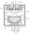
- FIG. 1is a schematic partial view of a cathode-coupled type plasma etching apparatus
- reference 1indicates a processing chamber of the plasma etching apparatus
- 2indicates a lower electrode provided in the processing chamber 1
- 3indicates a guide ring member securely mounted on the lower electrode 2 to position an object such as a silicon wafer W to be subjected to an plasma etching process in place on the lower electrode 2
- 4indicates an upper electrode provided in the processing chamber 1 above the lower electrode 2 .
- the guide ring member 3is formed of a dielectric material such as ceramic. Also, note that the lower and upper electrodes 2 and 4 are coated with a dielectric material such as aluminum oxide (Al 2 O 3 ), so that dielectric layers 2 A and 4 A are formed thereon.
- a dielectric materialsuch as ceramic.
- the cathode-coupled type plasma etching apparatus of FIG. 1is provided with a DC power source 5 which is connected to the lower electrode 2 through a resistor 6 , and which applies an electrostatic chuck (ESC) voltage V ESC to the lower electrode 2 so that the silicon wafer W is electrostatically and tightly held by the lower electrode 2 .
- a DC power source 5which is connected to the lower electrode 2 through a resistor 6 , and which applies an electrostatic chuck (ESC) voltage V ESC to the lower electrode 2 so that the silicon wafer W is electrostatically and tightly held by the lower electrode 2 .
- ESCelectrostatic chuck
- the cathode-coupled type plasma etching apparatus of FIG. 1is provided with an AC power source 7 which is connected to the lower electrode 2 through a capacitor 8 , and which applies a radio frequency (RF) voltage V RF to the lower electrode 2 so that a plasma PL is generated between the lower and upper electrodes 2 and 4 .
- RFradio frequency
- the silicon wafer Wcaptures electrons so that the lower electrode 2 with the silicon wafer W is negatively self-biased, with the lower and upper electrodes 2 and 4 serving as anode and cathode electrodes, respectively.
- reference Eindicates an electric field generated between the lower and upper electrodes 2 and 4 due to both the ESC voltage V ESC and the self-biased voltage of the lower electrode 2 with the silicon wafer W.
- reaction productssuch as tungsten fluoride or titanium fluoride are produced in the processing chamber 1 , and are deposited on the guide ring member 3 and the dielectric layer 4 A of the upper electrode 4 , so that reaction product deposits or dielectric deposits D 1 and D 2 are formed on the top surface of the guide ring member 3 and the bottom surface of the dielectric layer 4 A, respectively.
- the permittivity of the dielectric deposits D 1 and D 2is smaller than that of the guide ring member 3 , and is smaller than that of the dielectric layer 4 A.
- the first term “ ⁇ E”represents a Coulomb force per unit volume, but the Coulomb force per unit volume can be ignored because the true electric charge density is substantially zero in the dielectric deposit D 1 or D 2 .
- the second term “(1 ⁇ 2)E 2 ⁇ ”represents a Maxwell stress
- the third term “(1 ⁇ 2) ⁇ [E 2 m(d ⁇ /dm)]”represents a Helmholtz stress.
- particles derived from the dielectric deposit D 1 or D 2may be produced in the processing chamber 1 when the dielectric deposit D 1 or D 2 are peeled from the guide ring member 6 or the bottom surface of the dielectric layer 4 A due to both the Maxwell stress and the Helmholtz stress.
- reference OAindicates an observation area which is predetermined to observe particles.
- the application of the RF voltage V RF to the lower electrode 2was carried out at 600 Watts to thereby generate the plasma PL.
- the lower electrode 2 no with the silicon wafer Wexhibited a self-biased voltage falling within the range between ⁇ 100 volts and ⁇ 200 volts, and the plasma PL exhibited a plasma potential of about 10 volts.
- the particlesare subjected to a repelling force based on the Maxwell stress, due to the fact that the guide ring member 3 has a larger permittivity than that of the dielectric deposit D 1 .
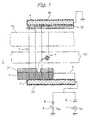
- the inventorsconducted experiments and research into the relationship between the ESC voltage V RF applied to the lower electrode 2 and the number of particles, by using the cathode-coupled type plasma etching apparatus of FIG. 1 in which fifty sample silicon wafers W were individually processed, with the ESC voltage V ESC varying within an excessively wide range from about ⁇ 1250 to about +1000 volts.
- FIG. 2Ais a graph showing the experimental results.
- the abscissarepresents the ESC voltage V ESC
- the ordinaterepresents the number of particles per the fifty silicon wafers W which were individually processed.
- the number of particlesvaried in accordance with a curve a secondary degree having the minimum value at ⁇ 150 volts. Namely, the number of particles was increased in proportion to the square value of the ESC voltage V ESC . This proved that the particles were subjected to the repelling force based on the Maxwell stress, with the repelling force being in proportion to the square value of the electric field E.
- FIG. 2Bis a graph showing the experimental results.
- the abscissarepresents the time; the left ordinate represents the number of particles; and the right ordinate represents the ESC voltage V ESC applied to the lower electrode 2 , the pressure in the processing chamber 1 , and the RF voltage V RF applied to the lower electrode 2 .
- the ESC voltage V ESCwas set so that each of the sample silicon wafers W was suitably held by the lower electrode 2 .
- the Helmholtz stresscauses changes in volume of both the dielectric layer 4 A of the upper electrode 4 and the dielectric deposit D 2 , and the Helmholtz stress acts as a force pressing the dielectric deposit D 2 against the dielectric layer 4 A due to the fact that the permittivity of the dielectric layer 4 A is larger than that of the dielectric deposit D 2 .
- the volume of the dielectric layer 4 A and the dielectric deposit D 2are changed, particles derived from the dielectric deposit D 2 may be produced in the boundary therebetween, but these particles cannot be released in the processing chamber 1 due to the fact that the dielectric deposit D 2 is pressed against the dielectric layer 4 A.
- the application of the RF voltage V RFis stopped so that the plasma PL disappears, the force pressing the dielectric deposit D 2 against the dielectric layer 4 A is canceled, resulting in the release of the particles in the processing chamber 1 .
- each of the m(d ⁇ /dm) valuesis larger than the corresponding permittivity ⁇ .
- the reaction product deposits D 1 and D 2are dominated by the Helmholtz stress rather than the Maxwell stress.
- a magnetic depositexists in an apparatus involving generation of a magnetic field, such as an electron microscopic apparatus, an electron cyclotron resonance (ECR) type plasma etching apparatus, a magnetic-field assist type plasma etching apparatus or the like.
- ECRelectron cyclotron resonance
- FIG. 3is a cross-sectional view of a first embodiment of the apparatus according to the present invention
- the first embodimentis constituted as an anode-coupled type plasma CVD apparatus.
- the anode-coupled type plasma CVD apparatusincludes a housing 10 having a bottom wall section 10 A, a side wall section 10 B and a top wall section 10 C which define a processing chamber 10 D.
- the housing 10itself is formed of a suitable metal material such as aluminum or the like, and the inner wall surfaces of the bottom, side aid top wall sections 10 A, 10 B and 10 C of the housing 10 are coated with silicon dioxide (SiO 2 ) so that silicon dioxide layers 10 E are formed thereon.
- the housing 10is provided with exhaust passages 10 F formed in the bottom wall section 10 A, and the exhaust passages 10 F are in communication with a vacuum source not shown) so that a vacuum state is created in the processing chamber 10 D.
- the housing 10is provided with a gas supply conduit 10 G connected to the bottom wall section 10 A at the center thereof so as to be in communication with the processing chamber 10 D.
- the gas supply conduit 10 Gis connected to a silane gas source and an oxygen gas source so that silane gas (SiH 4 ) and oxygen gas (O 2 ) are introduced into the processing chamber 10 D.
- the anode-coupled type plasma CVD apparatus of FIG. 3also includes electric heaters 11 provided on the bottom wall section 10 A around the gas supply conduit 10 G, and lower electrodes 12 provided on the respective electric heaters 11 .
- the lower electrodesthemselves are formed of a suitable metal such as aluminum or the like, and both a bottom surface and a side surface of each of the lower electrodes 12 are coated with silicon dioxide (SiO 2 ) so that a silicon dioxide layer 12 A is formed thereon.
- the anode-coupled type plasma CVD apparatus of FIG. 3further includes susceptors 13 provided on the respective lower electrodes 12 , and each of the susceptors 13 is formed of silicon dioxide (SiO 2 ). Objects such as silicon wafers W to be processed are placed on the respective susceptors 13 .
- the anode-coupled type plasma CVD apparatus of FIG. 3is provided with a DC power source 14 which is connected to the lower electrodes 12 through a resistor 15 , and which applies an ESC voltage V ESC to the lower electrodes 12 so that the silicon wafers W are electrostatically and tightly held by the respective susceptors 13 , whereby the silicon wafers W can be uniformly heated by the respective electric heaters 11 .
- the anode-coupled type plasma CVD apparatus of FIG. 3further includes an upper electrode 16 which is suspended from the top wall section 10 C of the housing 10 so as to oppose the lower electrodes 12 .
- the upper electrode 16is connected to a lower end of a conductive stem 17 which is securely set in the top wall section 10 C.
- the upper electrode 16is coated with silicon dioxide (SiO 2 ) so that a silicon dioxide layer 16 A is formed thereon.
- the anode-coupled type plasma CVD apparatus of FIG. 3is provided with an AC power source 19 which is connected to the conductive stem 17 through a capacitor 18 , and an RF voltage V RF is applied to the upper electrode 16 so that a plasma (not shown) is generated between the loiter electrodes 12 and the upper electrode 16 .
- V RFRF voltage
- the silicon wafers Wcapture electrons so that the lower electrodes 12 with the silicon wafers W are negatively self-biased. Namely, the lower electrodes 12 with the silicon wafers W serve as cathode electrodes, and the upper electrode 16 serves as an anode electrode.
- silane gas (SiH 4 ) and oxygen gas (O 2 )are introduced into the processing chamber 10 D through the gas supply conduit 10 G, and thus silicon dioxide substance is produced as a reaction product in the processing chamber 10 D.
- a part of the silicon dioxide substanceis deposited on the silicon loafers W so that silicon dioxide film layers are formed on the silicon wafers W.
- silicon dioxide substanceis deposited on various internal members such as the lower electrodes 12 , the susceptors 13 , the upper electrode 16 and so on, so that silicon dioxide deposits are formed on the various internal members 12 , 13 and 16 .
- yet another part of the silicon dioxide substanceis deposited on the dielectric layers 10 E on the inner wall surfaces of the bottom, side and top wall sections 10 A, 10 B and 10 C of the housing 10 , so that silicon dioxide deposits are formed thereon.
- each of the bottom, side and top wall sections 10 A, 10 B and 10 C of the housing 10is defined as an internal member.
- the silicon dioxide layers 10 Eare formed on the inner wall surfaces of the bottom, side and top wall sections 10 A, 10 B and 10 C of the housing 10 .
- the silicon dioxide layers 12 Aare formed on the lower electrodes 12
- the silicon dioxide layer 16 Ais formed on the upper electrode 16 .
- the susceptors 13themselves are formed of silicon dioxide (SiO 2 ).
- a part ( 10 A, 10 B, 10 C, 12 and 16 ) of the internal membersis coated with silicon dioxide (SiO 2 ), and the other part ( 13 ) of the internal members is formed of silicon dioxide (SiO 2 ).
- the silicon dioxide deposits deposited on the internal memberscannot be prevented from being peeled from the internal members. This is because the silicon dioxide deposits cannot be subjected to a force peeling the silicon dioxide deposits from the internal members due to the fact that the m(d ⁇ /dm) value of the silicon dioxide deposits coincides with that of the silicon dioxide layers 10 E, 12 A and 16 B and with that of the susceptors 13 . Thus, it is possible to considerably suppress production of particles deriving from the silicon dioxide deposits, resulting in protection of the silicon wafers W from being contaminated with the particles.
- the housing 10itself is preferably formed of aluminum exhibiting a superior thermal conductivity.
- the silicon dioxide layers 10 Emay be formed by using a sputtering process. In this case, it is possible to easily control a process temperature during an execution of the CVD process, due to the superior thermal, conductivity of the housing 10 .
- the inner wall surfaces of the bottom, side and top wall sections 10 A, 10 B and 10 Cmay be coated with another dielectric material such as yttrium aluminum garnet (YAG) exhibiting an m(d ⁇ /dm) value smaller than that of silicon dioxide or the like.
- YAGyttrium aluminum garnet
- the coating of YAGis carried out by using a flame spray coating process so that porous YAG layers having a 50% porosity are formed on the inner wall surfaces of the bottom, side and top wall sections 10 A, 10 B and 10 C.
- Each of the porous YAG layers having the 50% porosityexhibits the m(d ⁇ /dm) value which is virtually equal to that of silicon dioxide. Note that the same is true for each of the silicon dioxide layers 12 A and 16 A of the lower and upper electrodes 12 and 16 .
- the inner wall surfaces of the bottom, side and top wall sections 10 A, 10 B and 10 Cmay be coated with a mixture of at least two kinds of dielectric materials except for silicon dioxide.
- the mixtureshould be prepared so as to exhibit an m(d ⁇ /dm) value which is substantially equal that of silicon dioxide. If a difference between the m(d ⁇ /dm) value of the mixture and the m(d ⁇ /dm) value of silicon dioxide falls within a range of ⁇ 5%, both the m(d ⁇ /dm) values can be regarded as being substantially equal to each other, so that it is possible to effectively suppress the production of particles. Note that the same is true for each of the silicon dioxide layers 12 A and 16 A of the lower and upper electrodes 12 and 16 .
- FIG. 4is a cross-sectional view of a second embodiment of the apparatus according to the present inventions the second embodiment is constituted as a cathode-coupled type plasma etching apparatus.
- the cathode-coupled type plasma etching apparatusincludes a housing 20 having a bottom wall section 20 A, a side wall section 20 B and a top wall section 20 C which define a processing chamber 20 D.
- the housing 20itself is formed of a suitable metal material such as aluminum or the like, and the inner wall surfaces of the bottom, side and top wall sections 20 A, 20 B and 20 C of the housing 20 are coated with a suitable dielectric material such as YAG, barium titanate (BaTiO 3 ), lead zirconate/titanate (Pb(Zr,Ti)O 3 ) or the like, so that dielectric layers 20 E are formed thereon.
- the side wall section 20 Bis provided with a gate valve 20 B′ which is openable for introducing an object such as a silicon wafer W to be processed into the processing chamber 20 D and for taking out the same from the processing chamber 20 D.
- An inner wall surface of the gate valve 20 Bis also coated with the aforesaid dielectric material such as YAG, barium titanate (BaTiO 3 ), lead zirconate/titanate (Pb(Zr,Ti)O 3 ) or the like, so that a dielectric layer 20 E′ is formed thereon.
- the silicon wafer Whas a multi-layered metal film layer structure to be etched, and the multi-layered metal film layer structure includes a titanium (Ti) film layer formed on the silicon wafer W, and a tungsten (W) film layer formed on the titanium (Ti) film layer.
- the housing 20is provided with an exhaust passage 20 F formed in the bottom wall 20 A, and the exhaust passage 20 F is in communication with a vacuum source (not shown) so that a vacuum state is created in the processing chamber 20 D.
- the cathode-coupled type plasma etching apparatus of FIG. 4includes an object-stage unit 21 provided in the bottom wall section 20 A, and a lower electrode 22 incorporated in the object-stage unit 21 , and the silicon wafer W to be processed is placed on the lower electrode 22 .
- the object-stage unit 21has a base member 21 A set in the bottom wall section 20 A, a cup-like member 21 B securely mounted on the base member 21 A, a conductive member 21 C received in the cup-like member 21 B, and a ring-like member 21 D securely mounted on the cup-like member 21 D so as to surround an upper portion of the conductive member 21 C.
- the lower electrode 22is provided on the conductive member 21 C, and is retained by the ring-like member 21 D.
- the ring-like member 21 Dserves as a guide ring member for positioning the silicon wafer W in place on the lower electrode 22 .
- the base member 21 A, the cup-like member 21 B and the ring-like member 21 Dare formed of the aforesaid dielectric material such as YAG, barium titanate (BaTiO 3 ), lead zirconate/titanate (Pb(Zr,Ti)O 3 ) or the like, and the conductive member 21 B is formed of a suitable metal material such as aluminum or the like.
- the cathode-coupled type plasma etching apparatus of FIG. 4is provided with a DC power source 23 1 which is connected to the conductive member 21 C through a resistor 23 2 so that an ESC voltage V ESC is applied to the lower electrode 22 through the conductive member 21 C, whereby the silicon wafer W is electrostatically and tightly held by the lower electrode 22 .
- the cathode-coupled type plasma etching apparatus of FIG. 4is provided with an AC power source 24 1 which is connected to the conductive member 21 C through a capacitor 24 2 , and an RF voltage V RF is applied to the lower electrode 22 .
- the cathode-coupled type plasma etching apparatus of FIG. 4further includes a conductive plug-like member 25 set in the top wall section 20 C of the housing 20 , an upper electrode 26 securely attached to the lower end face of the conductive plug-like member 25 , a gas plate 27 electrically and securely connected to the upper electrode 26 , and a ring-like member 28 securely attached to the peripheral sides of both the upper electrode 26 and the gas plate 27 .
- the upper electrode 26is grounded through the plug-like conductive member 25 , and thus a plasma (not shown) is generated between the lower and upper electrodes 22 and 26 when applying the RF voltage V RF to the lower electrode 22 .
- the lower and upper electrodes 22 and 26serve as cathode and anode electrodes, respectively.
- Both the plug-like member 25 and the upper electrode 26are formed with a gas supply passage 29 at the centers thereof, and a gas mixture containing sulfur hexafluoride gas and suitable additive gas is introduced as an etching gas into the processing chamber 20 D through the gas supply passage 29 .
- the plug-like member 25 , the upper electrode 26 and the gas plate 27are formed of a suitable metal material such as aluminum or the like, and are coated with the aforesaid dielectric material such as YAG, barium titanate (BaTiO 3 ), lead zirconate/titanate (Pb(Zr,Ti)O 3 ) or the like, so that dielectric layers 25 A, 26 A and 27 A are formed thereon, whereby the metal surfaces of the plug-like member 25 , the upper electrode 26 and the gas plate 27 are prevented from being directly exposed.
- a suitable metal materialsuch as aluminum or the like
- the ring-like member 28is formed of the aforesaid dielectric material such as YAG, barium titanate (BaTiO 3 ), lead zirconate/titanate (Pb(Zr,Ti)O 3 ) or the like.
- tungsten fluoride (WF 6 )exhibits a low boiling plaints (16.9° C.) it is discharged from the processing chamber 20 D through the exhaust passage 20 F. Namely, the reaction products except for tungsten fluoride (WF 6 ) are left as dielectric substances in the processing chamber 20 D.
- a part of the dielectric substancesis deposited on various internal members such as the base member 21 A, the cup-like member 21 B, the ring-like member 21 D, the conductive plug-like member 25 , the upper electrode 26 , the gas plate 27 and the ring-like member 28 , so that dielectric deposits are formed on the various internal members.
- dielectric layers 20 Eare deposited on the dielectric layers 20 E on the inner wall surfaces of the bottom, side and top wall sections 20 A, 20 B and 20 C of the housing 20 , so that dielectric deposits are formed on the bottom, side and top wall sections 10 A, 10 B and 10 C.
- each of the bottom, side and top wall sections 20 A, 20 B and 20 C of the housing 20is defined as an internal member.
- titanium fluoride (TiF 3 )forms a main component of the dielectric deposits formed on the internal members.
- the aforesaid dielectric materialsuch as YAG, barium titanate (BaTiO 3 ), lead zirconate/titanate (Pb(Zr,Ti)O 3 ) or the like is selected so as to have a smaller m(d ⁇ /dm) value than that of the dielectric deposits formed on the internal members.
- the dielectric depositsare subjected to forces peeling them from the internal members, so that particles are produced in the processing chamber 20 D.
- the silicon wafer Wis protected from being contaminated with the particles because the particles are positively charged so as to be repelled by the plasma having the positive potential. Namely, the particles are discharged from the processing chamber 20 D through the exhaust passage 20 F without they reaching the silicon wafer W.
- the m(d ⁇ /dm) value of the dielectric depositsis calculated based on a permittivity and an expansion coefficient of the dielectric deposits actually measured. Nevertheless, the m(d ⁇ /dm) value of the dielectric deposits may be represented by an (d ⁇ /dm) value of the main component (titanium fluoride (TiF 3 ) or tungsten fluoride (WF 3 )) of the dielectric deposits. Otherwise, the m(d ⁇ /dm) value of the dielectric deposits may be represented by an average of m(d ⁇ /dm) values of some components of the dielectric deposits.
- TiF 3titanium fluoride
- WF 3tungsten fluoride
- FIG. 5is a cross-sectional view of a third embodiment of the apparatus according to the present invention
- the third embodimentis also constituted as a cathode-coupled type plasma etching apparatus.
- the cathode-coupled type plasma etching apparatusincludes a housing 30 having a bottom wall section 30 A, a side wall section 30 B and a top wall section 30 C which define a processing chamber 30 D.
- the housing 30itself is formed of a suitable metal material such as aluminum or the like.
- the inner surface of the bottom wall section 30 Ais coated with a first type dielectric material such as titanium dioxide (TiO 2 ), potassium dihydrogenphosphate (KH 2 PO 4 ), barium zirconate (PbZrO 3 ) or the like, so that a dielectric layer 30 A 1 is formed thereon.
- a lower area of the inner surface of the side wall section 30 Bis also coated with the aforesaid first type dielectric material such as titanium dioxide (TiO 2 ), potassium dihydrogenphosphate (KH 2 PO 4 ), barium zirconate (PbZrO 3 ) or the like, so that a dielectric layer 30 B 1 is formed thereon.
- an upper area of the inner surface of the side wall section 30 Bis coated with a second type dielectric material such as YAG, barium titanate (BaTiO 3 ), lead zirconate/titanate (Pb(Zr,Ti)O 3 ) or the like, so that a dielectric layer 30 B 2 is formed thereon.
- the inner surface of the top wall section 30 Cis also coated with the aforesaid type second dielectric material such as YAG, barium titanate (BaTiO 3 ), lead zirconate/titanate (Pb(Zr,Ti)O 3 ) or the like, so that a dielectric layer 30 C 2 is formed thereon.
- the side wall section 30 Bis provided with a gate valve 30 B′ which is openable for introducing an object such as a silicon wafer W to be processed into the processing chamber 30 D and for taking out the same from the processing chamber 30 D.
- An inner wall surface of the gate valve 30 B′is coated with the aforesaid first type dielectric material such as titanium dioxide (TiO 2 ), potassium dihydrogenphosphate (KH 2 PO 4 ), barium zirconate (PbZrO 3 ) or the like, so that a dielectric layer 30 B 1 ′ is formed thereon.
- the silicon wafer Whas a multi-layered metal film layer structure to be etched, and the multi-layered metal film layer structure includes a titanium (Ti) film layer formed on the silicon wafer W, and a tungsten (W) film layer formed on the titanium (Ti) film layer.
- the housing 30is provided with an exhaust port 30 E formed in the bottom wall section 30 A, and the exhaust port 30 E is in communication with a vacuum source (not shown) so that a vacuum state is created in the processing chamber 30 D.
- the cathode-coupled type plasma etching apparatus of FIG. 5includes an object-stage unit 31 provided in the bottom wall section 30 A, and a lower electrode 32 incorporated in the object-stage unit 31 , and the silicon wafer W to be processed is placed on the lower electrode 32 .
- the object-stage unit 31has a base member 31 A set in the bottom wall section 30 A 1 a cup-like member 31 B securely mounted on the base member 31 A, a conductive member 31 C received in the cup-like member 31 B, a ring-like member 31 D securely mounted on the cup-like member 31 D so as to surround an upper portion of the conductive member 31 C, and a guide ring member 31 E securely mounted on the ring-like member 31 D.
- the lower electrode 32is provided on the conductive member 31 C, and is retained by the guide ring member 31 E to thereby position the silicon wafer W in place on the lower electrode 32 .
- the base member 31 A, the cup-like member 31 B, the ring-like member 31 D and the guide ring member 31 Eare formed of the aforesaid second type dielectric material such as dielectric material such as titanium dioxide (TiO 2 ), potassium dihydrogenphosphate (KH 2 PO 4 ), barium zirconate (PbZrO 3 ) or the like, and the conductive member 31 B is formed of a suitable metal material such as aluminum or the like.
- dielectric materialsuch as titanium dioxide (TiO 2 ), potassium dihydrogenphosphate (KH 2 PO 4 ), barium zirconate (PbZrO 3 ) or the like
- the conductive member 31 Bis formed of a suitable metal material such as aluminum or the like.
- the cathode-coupled type plasma etching apparatus of FIG. 5is provided with a DC power source 33 1 which is connected to the conductive member 31 C through a resistor 33 2 so that an ESC voltage V ESC is applied to the lower electrode 32 through the conductive member 31 C, whereby the silicon wafer W is electrostatically and tightly held by the lower electrode 32 .
- the cathode-coupled type plasma etching apparatus of FIG. 5is provided with an AC power source 34 1 which is connected to the conductive member 31 C through a capacitor 34 2 , and an RF voltage V RF is applied to the lower electrode 32 .
- the cathode-coupled type plasma etching apparatus of FIG. 5further includes a conductive plug-like member 35 set in the top wall section 30 C of the housing 30 1 an upper electrode 36 securely attached to the lower end face of the conductive plug-like member 35 , and a gas plate 37 electrically and securely connected to the upper electrode 36 .
- the upper electrode 36is grounded through the plug-like conductive member 35 , and thus a plasma (not shown) is generated between the lower and upper electrodes 32 and 36 when applying the RF voltage V RF to the lower electrode 32 .
- the lower and upper electrodes 32 and 36serve as cathode and anode electrodes, respectively.
- Both the plug-like member 35 and the upper electrode 36are formed with a gas supply passage 38 at the centers thereof, and a gas mixture containing sulfur hexafluoride gas and suitable additive gas is introduced as an etching gas into the processing chamber 30 D through the gas supply passage 38 .
- the plug-like member 35 , the upper electrode 36 and the gas plate 37are formed of a suitable metal material such as aluminum or the like, and are also coated with the aforesaid second type dielectric material such as YAG, barium titanate (BaTiO 3 ), lead zirconate/titanate (Pb(Zr,Ti)O 3 ) or the like, so that dielectric layers 35 A 2 , 36 A 2 and 37 A 2 are formed thereon, whereby the metal surfaces of the plug-like member 35 , the upper electrode 36 and the gas plate 37 are prevented from being directly exposed.
- YAGbarium titanate
- Pb(Zr,Ti)O 3lead zirconate/titanate
- the cathode-coupled type plasma etching apparatus of FIG. 5when the multi-layered metal film layer structure on the silicon wafer W, which includes the titanium (Ti) film layer and the tungsten (W) film layer formed thereon, is subjected to a plasma etching process by using the etching gas containing the sulfur hexafluoride gas and the suitable additive gas, reaction products such as tungsten fluoride (WF 6 ), titanium fluoride (TiF 3 , TiF 4 ), titanium dioxide (TiO 2 ), sulfur (S) and so on are produced.
- WF 6tungsten fluoride
- TiF 3titanium fluoride
- TiO 2titanium dioxide
- Ssulfur
- tungsten fluoride (WF 6 )exhibits a low boiling points (16.9° C.), it is discharged from the processing chamber 20 D through the exhaust passage 20 F. Namely, the reaction products except for tungsten fluoride (WF 6 ) are left as dielectric substances in the processing chamber 20 D.
- a part of the dielectric substancesis deposited on the various internal members such as the base member 31 A, the cup-like member 31 B, the ring-like member 31 D, the guide ring member 31 E, the conductive plug-like member 35 , the upper electrode 36 and the gas plate 37 , so that dielectric deposits are formed on the various internal members.
- dielectric layers 30 A 1 , 30 B 1 , 30 B 2 and 30 C 2are deposited on the dielectric layers 30 A 1 , 30 B 1 , 30 B 2 and 30 C 2 on the bottom, side and top wall sections 30 A, 30 B and 30 C of the housing 30 , so that dielectric deposits are formed thereon.
- each of the bottom, side and top wall sections 30 A, 30 B and 30 C of the housing 30is defined as an internal member.
- titanium fluoride (TiF 3 )forms a main component of the dielectric deposits formed on the internal members.
- the aforesaid first type dielectric materialsuch as titanium dioxide (TiO 2 ), potassium dihydrogenphosphate (KH 2 PO 4 ), barium zirconate (PbZrO 3 ) or the like is selected so as to have a larger m(d ⁇ /dm) value than that the dielectric deposits deposited on the internal members.
- the aforesaid second type dielectric materialsuch as YAG, barium titanate (BaTiO 3 ), lead zirconate/titanate (Pb(Zr,Ti)O 3 ) or the like is selected so as to have a smaller m(d ⁇ /dm) value than that the dielectric deposits deposited on the internal members.
- the dielectric depositswhich are deposited on the dielectric layers 30 A 1 , 30 B 1 and 30 B 1 ′ and the internal members 31 A, 31 B, 31 D and 31 E, are subjected to forces pressing them against these internal members, respectively, so that particles cannot be produced from theme dielectric deposits concerned.
- the dielectric depositswhich are deposited on the dielectric layers 30 B 2 , 30 C 2 , and 35 A 2 , 36 A 2 and 37 A 2 , are subjected to forces peeling them from the internal members, so that particles are produced in the processing chamber 20 D.
- the production of the particlesis suppressed in a lower space of the processing chamber 30 D below the guide ring member 31 E, due to the pressing force exerted on the dielectric deposits, whereas the production of the particles is activated in an upper space of the processing chamber 30 D above the guide ring member 31 E.
- the particlesare produced in the lower space of the processing chamber 30 D, a part of the particles is apt to be intruded into a space between the plasma and the silicon wafer W, and thus the intruded particles are electrically attracted to the silicon wafer W which is negatively self-biased. Nevertheless, in reality, the attraction of the particles to the silicon wafer W is effectively prevented because the production of the particles is suppressed in the lower space of the processing chamber 30 D.
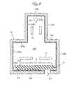
- FIG. 6is a cross-sectional view of a fourth embodiment of the apparatus according to the present inventions the fourth embodiment is constituted as a thermal CVD apparatus.
- the thermal CVD apparatusincludes a housing 40 having a bottom wall section 40 A, a side wall section 40 B and a top wall section 40 C which define a processing chamber 40 D.
- the housing 40itself is formed of a suitable metal material such as aluminum or the like, and the inner wall surfaces of the bottom, side and top wall sections 40 A, 40 B aid 40 C of the housing 40 are coated with a suitable dielectric material, so that silicon dioxide layers 40 E are formed thereon.
- the housing 40is provided with exhaust passages 40 F formed in the bottom wall section 10 A, and the exhaust passages 40 F are in communication with a vacuum source (not shown) so that a vacuum state is created in the processing chamber 40 D.
- the housing 40is provided with a gas supply conduit 40 G integrally provided in the top wall section 40 C.
- start gases for the CVD processare introduced into the processing chamber 40 D through the gas supply conduit 40 G.
- a cleaning gasis introduced into the processing chamber 40 D through the gas supply conduit 40 G.
- the dielectric layer 40 E formed on the inner surface of the top wall section 40 Cis extended so that an inner surface of the gas supply conduit 40 G is covered with the extension thereof.
- the thermal CVD apparatus of FIG. 6also includes electric heaters 41 provided on an outer surface of the bottom wall section 40 A, an lower electrode 42 provided on an inner surface of the bottom wall section 40 A, and a susceptor 43 provided on the respective lower electrodes 42 .
- an objectsuch as a silicon wafer to be processed is placed on the susceptor 43 .
- the lower electrode 42itself is formed of a suitable metal such as aluminum or the like, and both a bottom surface and a side surface of the lower electrodes 12 are coated with a suitable dielectric material so that a dielectric layer 42 A is formed thereon.
- the dielectric material of the dielectric layer 42 Amay be the same as that of the dielectric layers 40 E.
- the susceptor 43is formed of a suitable dielectric material, and the dielectric material of the susceptor 43 may be the same as that of the dielectric layers 40 E.
- the thermal CVD apparatusmay be provided with a DC power source which is connected to the lower electrodes 42 through a resistor, and which applies an ESC voltage to the lower electrodes 42 so that the silicon wafer (not shown) is electrostatically and tightly held by the susceptor 43 , whereby the silicon wafer can be uniformly heated by the electric heater 41 .
- the thermal CVD apparatus of FIG. 6further includes an upper electrode 44 which is suspended from the top wall section 40 C of the housing 40 so as to oppose the lower electrodes 42 .
- the upper electrode 44is connected to a lower end of a conductive stem 45 which is extended through the gas supply conduit 40 G, and which is supported by a suitable support member (not shown).
- the thermal CVD apparatus of FIG. 6is provided with an AC power source 46 which is connected to the conductive stem 45 through a capacitor 47 , and an RF voltage V RF is applied to the upper electrode 44 so that a plasma (not shown) is generated between the lower electrodes 42 and the upper electrode 44 during the execution of the CVD process.
- the upper electrode 44is suitably perforated, and thus serves as a gas plate for uniformly distributing the start gases in the processing chamber 40 D.
- the upper electrode 44is coated with a suitable dielectric material so that a dielectric layer 44 A is formed thereon.
- the dielectric material of the dielectric layer 44 Amay be the same as that of the dielectric layers 40 E.
- the conductive stem 45is coated with a suitable dielectric material so that a dielectric layer 45 A is formed thereon.
- the dielectric material of the dielectric layer 45 Amay be the same as that of the dielectric layers 40 E.
- reaction products or dielectric substanceswhich are derived from the start gases, are deposited on various internal members such as the susceptor 43 , the upper electrode 44 , the conductive stem 45 and so on, so that dielectric deposits are formed thereon. Also, a part of the dielectric substances is deposited on the dielectric layers 40 E on the inner wall surfaces of the bottom, side and top wall sections 40 A, 40 B and 40 C of the housing 40 , so that dielectric deposits are formed thereon.
- each of the bottom, side and top wall sections 40 A, 40 B and 40 C of the housing 40is defined as an internal member.
- the aforesaid vacuum source(not shown) is driven so that a vacuum state is created in the processing chamber 40 D.
- the lower electrode 42 and the housing 40are grounded as shown in FIG. 6 , and the RF voltage is applied to the upper electrode 44 to thereby create a plasma in the processing chamber 40 D.
- a suitable cleaning gassuch as a perfluorocarbon gas, a perfluoroethane gas, a perfluoropropane gas, a nitrogen trifluoride gas, a carbonyl fluoride gas or the like is introduced as an etching gas into the processing chamber 40 D through the gas supply conduit 40 G.
- the cleaning of the processing chamber 40 Dis carried out by etching the dielectric deposits formed on the internal members.
- the dielectric material of the dielectric layers 40 E, the susceptor 43 , the dielectric layers 44 A and 45 Ais selected as one having a smaller m(d ⁇ /dm) value than that of the dielectric deposits formed on the internal members.
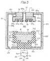
- FIG. 7is a cross-sectional view of a fifth embodiment of the apparatus according to the present invention
- the fifth embodimentis constituted as a focused ion beam (FIB) apparatus.
- FIBfocused ion beam
- the FIB apparatusincludes a housing 50 having a bottom wall section 50 A, a side wall section 50 B, a ceiling wall section 50 C, a cylindrical wall section 50 D and a top wall section 50 E which define a processing chamber 50 F.
- the housing 50itself is formed of a suitable metal such as aluminum or the likes and inner surfaces of the wall sections 50 A, 50 B, 50 C, 50 D and 50 E are coated with a suitable dielectric material so that respective dielectric layers 50 G 1 , 50 G 2 , 50 G 3 , 50 G 4 and 50 G 5 are formed thereon.
- the housing 50is provided with an exhaust port 50 H formed in the side wall section 50 B, and the exhaust port 50 H is in communication with a vacuum source (not shown) so that a vacuum state is created in the processing chamber 50 F.
- the FIB apparatus of FIG. 7also includes an object-stage unit 51 provided on the bottom wall section 50 A, and the object-stage unit 31 has a base member 51 A fixed on the bottom wall section 50 A, and a susceptor 51 B securely mounted on the base member 51 A.
- An objectsuch as a semiconductor chip C to be processed is placed oil the susceptor 51 B.
- Both the base member 51 A and the susceptor 51 Bare formed of a suitable dielectric material.
- the dielectric material of both the base member 51 A and the susceptor 51 Bmay be the same as that of the dielectric layers 50 G 1 , 50 G 2 , 50 G 3 , 50 G 4 and 50 G 5 .
- the FIB apparatus of FIG. 7further includes an ion source 52 provided in the processing chamber 50 F in the vicinity of the top wall section 50 E, and the ion source 52 emits ions.
- the ion source 52is suitably supported by support members securely attached to the cylindrical wall section 50 D. If necessary, the support members are coated with the same dielectric material as that of the dielectric layers 50 G 1 , 50 G 2 , 50 G 3 , 50 G 4 and 50 G 5 .
- the FIB apparatus of FIG. 7further includes an ion beam control unit 53 provided in the space defined by the cylindrical wall section 50 D.
- the ion beau control unit 53By the ion beau control unit 53 , the ions emitted from the ion source 52 are shaped into an ion beam IL, and the ion beam IL is controlled so that the semiconductor chip C is irradiated with the ion beam IL.
- the ion beam control unit 53includes a condenser lens 53 A, a beam blanker 53 B, an aligner 53 C, an object lens 53 D and a beam deflector 53 E, which are aligned with each other between the susceptor 51 and the ion source 52 .
- the ion beam control unit 53is suitably supported by support members securely attached to the cylindrical wall section 50 D. If necessary, the support members are coated with the same dielectric material as that of the dielectric layers 50 G 1 , 50 G 2 , 50 G 3 , 50 G 4 and 50 G 5 .
- the semiconductor chip Cis irradiated with the ion beam IL
- various dielectric substancesare produced from the semiconductor chip C due to the sputtering effect.
- the dielectric substancesare deposited on various internal members such as the base member 51 A, the susceptor 51 B the aforesaid support members and so on, so that dielectric deposits are formed thereon.
- a part of the dielectric substancesis deposited on the dielectric layers 50 G 1 , 50 G 2 , 50 G 3 , 50 G 4 and 50 G 5 on the wall sections 50 A, 50 B, 50 C, 50 D and 50 E of the housing 50 , so that dielectric deposits are formed thereon.
- each of the wall sections 50 A, 50 B, 50 C, 50 D and 50 E of the housing 50is defined as an internal member.
- Electric fieldsare generated in the processing chamber 50 F by both the ion source 52 and the ion control unit 53 , and thus the dielectric deposits are subjected to the Helmholtz stress.
- the dielectric layers 50 G 1 , 50 G 2 , 50 G 3 , 50 G 4 and 50 G 5have an m(d ⁇ /dm) value which is substantially equal to that of the dielectric deposits formed on the internal members, so that it is possible to suppress production of particles from the dielectric deposits, whereby the semiconductor chip C can be protected from being contaminated with the particles.
- FIG. 8is a cross-sectional view of a sixth embodiment of the apparatus according to the present invention
- the sixth embodimentis constituted as an electron beam (EB) exposure apparatus.
- EBelectron beam
- the EB apparatusincludes a housing 60 having a bottom wall section 60 A, a side wall section 60 B, a ceiling wall section 60 C, a cylindrical wall section 60 D and a top wall section 60 E which define a processing chamber 60 F.
- the housing 60itself is formed of a suitable metal such as aluminum or the like, and inner surfaces of the wall sections 60 A, 60 B, 60 C, 60 D and 60 E are coated with a suitable dielectric material so that respective dielectric layers 60 G 1 , 60 G 2 , 60 G 3 , 60 G 4 and 60 G 5 are formed thereon.
- the housing 60is provided with an exhaust port 60 H formed in the bottom wall section 60 A, and the exhaust port 60 H is in communication with a vacuum source (not shown) so that a vacuum state is created in the processing chamber 60 F.
- the EB exposure apparatus of FIG. 8also includes an object-stage unit 61 provided on the bottom wall section 60 A, and the object-stage unit 31 has a base member 61 A fixed on the bottom wall section 60 A, and an object stage 61 B securely mounted on the base member 61 A.
- An objectsuch as a silicon wafer W to be subjected to an exposure process is placed on the object stage 61 B. Namely, the silicon wafer W has a photoresist layer to be exposed.
- Both the base member 61 A and the object stage 61 Bare formed of a suitable dielectric material.
- the dielectric material of both the base member 61 A and the object stage 61 Bmay be the same as that of the dielectric layers 60 G 1 , 60 G 2 , 60 G 3 , 60 G 4 and 60 G 5 .
- the EB exposure apparatus of FIG. 8further includes an electron gun 62 provided in the processing chamber 60 F in the vicinity of the top wall section 60 E, and the electron gum 62 emits an electron beam toward the silicon wafer W.
- this electron gun 62is suitably supported by support members securely attached to the cylindrical wall section 60 D. If necessary, the support members are coated with the same dielectric material as that of the dielectric layers 60 G 1 , 60 G 2 , 60 G 3 , 60 G 4 and 60 G 5 .
- the EB exposure apparatus of FIG. 8further includes an electric field lens 63 provided in the processing chamber 60 F in the vicinity of the electron gun 62 , aid an electric field lens 64 provided in the processing chamber 60 F in the vicinity of the object-stage unit 61 .
- the electric field lenses 63 and 64the electron beam is controlled so that the silicon wafer W is scanned with the electron beam, whereby the photoresist layer on the silicon wafer W is exposed with the scanning electron beam.
- the electric field lens 63is suitably supported by support members securely attached to the cylindrical wall section 60 D, and the electric field lens 64 is suitably supported by support members securely attached to the side wall section 60 B. If necessary, the support members are coated with the same dielectric material as that of the dielectric layers 60 G 1 , 60 G 2 , 60 G 3 , 60 G 4 and 60 G 5 .
- dielectric substancesare deposited on the dielectric layers dielectric layers 60 G 1 , 60 G 2 , 60 G 3 , 60 G 4 and 60 G 5 of the wall sections 60 A, 60 B, 60 C, 60 D and 60 E of the housing 60 , so that dielectric deposits are formed thereon.
- each of the wall sections 60 A, 60 B, 60 C, 60 D and 60 E of the housing 60is defined as an internal member.
- the dielectric material of the dielectric layers 60 G 1 , 60 G 2 , 60 G 3 , 60 G 4 and 60 G 5 , the base member 61 A, the object stage 61 B, the aforesaid support members and so onis selected so as to have an m(d ⁇ /dm) value which is larger than that of the dielectric deposits formed on the internal members, so that the dielectric deposits are pressed against the internal members during the exposure process.
- titanium dioxide (TiO 2 )may be used for the dielectric material.
- FIG. 9is a cross-sectional view of a seventh embodiment of the apparatus according to the present invention
- the seventh embodimentis constituted as an electron microscopic apparatus.
- the electron microscopic apparatus of FIG. 9includes a housing 70 having a bottom wall section 70 A, a side wall section 70 B, a ceiling wall section 70 C, a cylindrical wall section 70 D and a top wall section 70 E which define a processing chamber 70 F.
- the housing 70itself is formed of a suitable metal such as aluminum or the like, and inner surfaces of the wall sections 70 A, 70 B, 70 C, 70 D and 70 E are coated with a suitable magnetic material so that respective magnetic layers 70 G 1 , 70 G 2 , 70 G 3 , 70 G 4 and 70 G 5 are formed thereon.
- the housing 70is provided with an exhaust port 70 H formed in the bottom wall section 70 A, and the exhaust port 70 H is in communication with a vacuum source (not shown) so that a vacuum state is created in the processing, chamber 70 F.
- the electron microscopic apparatus of FIG. 9also includes an object-stage unit 71 provided on the bottom wall section 70 A, and the object-stage unit 31 has a base member 71 A fixed on the bottom wall section 70 A, and all object stage 71 B securely mounted on the base member 71 A.
- An objectsuch as a silicon wafer W to be observed is placed on the object stage 71 B.
- Both the base member 71 A and the object stage 71 Bare formed of a suitable magnetic material.
- the magnetic material of both the base member 71 A and the object stage 71 Bmay be the same as that of the magnetic layers 70 G 1 , 70 G 2 , 70 G 3 , 70 G 4 and 70 G 5 .
- the electron microscopic apparatus of FIG. 9further includes an electron gun 72 provided in the processing chamber 70 F in the vicinity of the top wall section 70 E, and the electron gum 72 emits an electron beam toward the silicon wafer W.
- the electron gun 72is suitably supported by support members securely attached to the cylindrical wall section 70 D. If necessary, the support members are coated with the same magnetic material as that of the magnetic layers 70 G 1 , 70 G 2 , 70 G 3 , 70 G 4 and 70 G 5 .
- the electron microscopic apparatus of FIG. 9further includes an electromagnetic lens 73 provided in the processing chamber 70 F in the vicinity of the electron gun 72 , and an electromagnetic lens 74 provided in the processing chamber 70 F in the vicinity of the object-stage unit 71 .
- the electromagnetic lenses 73 and 74the electron beam is controlled so that the silicon wafer W is scanned with the electron beam, and secondary electrons are generated from the silicon wafer W during the scanning of silicon wafer W with the electron beam.
- the electromagnetic lens 73is suitably supported by support members securely attached to the cylindrical wall section 70 D, and the electromagnetic lens 74 is suitably supported by support members securely attached to the side wall section 70 B. If necessary, the support members are coated with the same magnetic material as that of the magnetic layers 70 G 1 , 70 G 2 , 70 G 3 , 70 G 4 and 70 G 5 .
- the electron microscopic apparatus of FIG. 9further includes a secondary electron detector 75 which is provided beneath the electromagnetic lens 74 to detect the secondary electrons generated from the silicon wafer W.
- the secondary electron detector 75is suitably supported by support members securely attached to the side wall section 70 B. If necessary, the support members are coated with the same magnetic material as that of the magnetic layers 70 G 1 , 70 G 2 , 70 G 3 , 70 G 4 and 70 G 5 .
- processing chamber 70 FIn operation, although the processing chamber 70 F is in the vacuum state, some fine magnetic substances, which may be derived from the silicon wafer W, inevitable exist in the processing chamber 70 F.
- a part of the fine substancesare deposited on various internal members such as the base member 71 A, the object stage 71 B, the aforesaid support members and so on, so that magnetic deposits are formed thereon.
- each of the wall sections 70 A, 70 B, 70 C, 70 D and 70 E of the housing 70is defined as an internal member.
- Magnetic fieldsare generated in the processing chamber 70 F by the electromagnetic lenses 73 and 74 .
- the magnetic layers 70 G 1 , 70 G 2 , 70 G 3 , 70 G 4 and 70 G 5have an m(d ⁇ /dm) value which is substantially equal to that of the magnetic deposits formed on the internal members.
- FIG. 10is a cross-sectional view of an eighth embodiment of the apparatus according to the present invention
- the eighth embodimentis constituted as an electron cyclotron resonance (ECR) type plasma etching apparatus.
- ECRelectron cyclotron resonance
- the ECR type plasma etching apparatusincludes a housing 80 having a bottom wall section 80 A, a side wall section 80 B, a ceiling wall section 80 C, a cylindrical wall section 80 D and a top wall section 80 E which define a processing chamber 80 F.
- the housing 80itself is formed of a suitable metal such as aluminum or the like, and inner surfaces of the wall sections 80 A, 80 B, 80 C, 80 D and 80 E are coated with a suitable-table magnetic material so that respective magnetic layers 80 G 1 , 80 G 2 , 80 G 3 , 80 G 4 and 80 G 5 are formed thereon.
- the housing 80is provided with an exhaust port 80 H formed in the bottom wall section 80 A, and the exhaust port 80 H is in communication with a vacuum source not shown) so that a vacuum state is created in the processing chamber 80 F. Also, the housing 80 is provided with a gas supply port 80 I formed in the ceiling wall section 80 C, and the gas supply port 80 I is in communication with an etching gas source (not shown) so that an etching gas is introduced into the processing chamber 80 F through the gas supply part 80 I.
- the ECR type plasma etching apparatus of FIG. 10also includes an object-stage unit 81 provided on the bottom wall section 80 A, and a lower electrode 82 incorporated in the object-stage unit 81 .
- the object-stage unit 81has a base member 81 A fixed on the bottom wall section 81 A, an object stage member 81 B securely mounted on the base member 81 A, and a guide ring member 81 C securely mounted on that object stage member 81 B.
- the lower electrode 82is provided on the object so stage member 80 B, and is retained by the guide ring member 81 C.
- An object such as a silicon wafer W to be processedis placed on the lower electrode, and is positioned in plaice on the lower electrode 32 by the guide ring member 81 C.
- the ECR type plasma etching apparatus of FIG. 10is provided with a DC power source 83 1 which is connected to the lower electrodes 82 through a resistor 83 2 , and which applies an ESC voltage V ESC to the lower electrodes 82 so that the silicon wafers W are electrostatically and tightly held by the lower electrode 82 .
- the ECR type plasma etching apparatus of FIG. 10also includes an upper electrode 84 which is suspended from the top wall section 80 E or the housing 80 so as to oppose the lower electrodes 82 .
- the upper electrode 84is connected to a lower end of a conductive stem 85 which is securely set in the top wall section 80 E.
- the upper electrode 84is coated with a suitable magnetic material so that a magnetic layer 84 A is formed thereon.
- the ECR type plasma etching apparatus of FIG. 10is provided with an AC power source 86 1 which is connected to the conductive stem 85 through a capacitor 86 2 , and an RF voltage V RF is applied to the upper electrode 84 so that a plasma (not shown) is generated between the lower electrodes 82 and the upper electrode 84 .
- the silicon wafer Wcaptures electrons so that the lower electrode 82 with the silicon wafers W is negatively self-biased.
- the lower electrode 82 with the silicon wafer Wserves as a cathode electrode
- the upper electrode 84serves as an anode electrode.
- the ECR type plasma etching apparatus of FIG. 10further includes an outer electromagnet 87 provided at around the cylindrical wall section 80 D, and an inner electromagnet 88 provided in the processing chamber 80 F just alcove the object-stage unit 81 , to thereby generate a magnetic field in the processing chamber 80 F.
- the magnetic fieldhas a magnetic flux density on the order of several hundred Gs.
- various magnetic substancesmay be produced as reaction produces in the processing chamber 80 F.
- a part of the various magnetic substancesis deposited on various internal members such as the base member 81 A, the object stage 81 B, the guide ring 81 C, the upper electrode 84 , so that magnetic deposits are formed on the various internal members.
- the various magnetic substancesis deposited on the magnetic layers 80 G 1 , 80 G 2 , 80 G 3 , 80 G 4 and 80 G 5 on the inner wall surfaces of the wall sections 80 A, 80 B, 80 C, 80 D and 80 E of the housing 80 , so that magnetic deposits are formed thereon.
- each of the wall sections 80 A, 80 B, 80 C, 80 D and 80 E of the housing 80is defined as an internal members.
- the magnetic deposits formed on the internal membersare dominated by the magnetic field rather than the electric field due to the magnetic flux density on the order of several hundred Gs.
- the magnetic layers 80 G 1 , 80 G 2 , 80 G 3 , 80 G 4 , and 80 G 5 , the internal members 81 A, 81 B and 81 C and the magnetic layer 84 Ahave an m(d ⁇ /dm) value which is smaller than that of the magnetic deposits formed on the internal members.
- the magnetic depositsare subjected to the peeling force for peeling them from the internal members, and thus the particles are actively produced. Nevertheless, the particles can be discharged from the processing chamber 80 F through the exhaust port 80 H in a similar manner to that of the first embodiment of FIG. 3 , without the silicon wafer W being contaminated with the particles.
- the m(d ⁇ /dm) value of the magnetic depositsis calculated based on a permeability and an expansion coefficient of the magnetic deposits actually measured. Nevertheless, the m(d ⁇ /dm) value of the magnetic deposits may be represented by an m(d ⁇ /dm) value of a main component of the magnetic deposits. Otherwise, the m(d ⁇ /dm) value of the magnetic deposits may be represented lay an average of m(d ⁇ /dm) valves of some components of the magnetic deposits.
- FIG. 11is a cross-sectional view of a ninth embodiment of the apparatus according to the present invention
- the ninth embodimentis constituted as a magnetic-field assist type plasma etching apparatus.
- the magnetic-field assist type plasma etching apparatusincludes a housing 90 having a bottom wall section 90 A, a side wall section 90 B and a top wall section 90 C which define a processing chamber 90 D.
- the housing 90itself is formed of a suitable metal material such as aluminum or the like.
- the inner surfaces of the bottom, side and top wall sections 90 A, 90 B and 90 Care coated with a suitable magnetic material so that magnetic layers 90 E 1 , 90 E 2 and 90 E 3 are formed thereon.
- the side wall section 90 Bis provided with a gate valve 90 B′ which is openable for introducing an object such as a silicon wafer W to be processed into the processing chamber 90 D and for taking out the same from the processing chamber 90 D.
- the inner wall surface of the gate valve 90 B′is coated with a suitable magnetic material so that a magnetic layer 90 E′ is formed therein.
- the magnetic material of the magnetic layer 90 E′may be the same as that of the magnetic layers 90 E 1 , 90 E 2 and 90 E 3 .
- the housing 90is provided with an exhaust port 90 E formed in the bottom wall section 90 A, and the exhaust port 90 E is in communication with a vacuum source snot shown) so that a vacuum state is created in the processing chamber 90 D.
- the magnetic-field assist type plasma etching apparatus of FIG. 11includes an object-stage unit 91 provided in the bottom wall section 90 A, and a lower electrode 92 incorporated in the object-stage unit 91 , and the silicon wafer W to be processed is placed on the lower electrode 92 .
- the object-stage unit 91has a base member 91 A set in the bottom wall section 90 A, a cup-like member 91 B securely mounted on the base member 91 A, a conductive member 91 C received in the cup-like member 91 B, a ring-like member 91 D securely mounted on the cup-like member 91 B so as to surround an upper portion of the conductive member 91 C, and a guide ring member 91 E securely mounted on the ring-like member 91 D.
- the lower electrode 92is provided on the conductive member 91 C, and is retained by the guide ring member 91 E to thereby position the silicon wafer W in place on the lower electrode 92 .
- the base member 91 A, the cup-like member 91 B, the ring-like member 91 D and the guide ring member 91 Eare formed of a suitable magnetic material.
- the magnetic material of the base member 91 A, the cup-like member 91 B, the ring-like member 91 D and the guide ring member 91 Emay be the same as that of the magnetic layers 90 E 1 , 90 E 2 , and 90 E 3 .
- the magnetic-field assist type plasma etching apparatus of FIG. 11is provided with a DC power source 93 1 which is connected to the conductive member 90 C through a resistor 93 2 so that an ESC voltage V ESC is applied to the lower electrode 92 through the conductive member 91 C, whereby the silicon wafer W is electrostatically and tightly held by the lower electrode 92 .
- the magnetic-field assist type plasma etching apparatus of FIG. 11is provided with an AC power source 94 1 which is connected to the conductive member 91 C through a capacitor 94 2 , end an RF voltage V RF is applied to the lower electrode 92 .
- the magnetic-field assist type plasma etching apparatus of FIG. 11further includes a conductive plug-like member 95 set in the top wall section 90 C of the housing 90 , an upper electrode 96 securely attached to the lower end face of the conductive plug-like member 95 , and a as plate 97 electrically and securely connected to the upper electrode 96 .
- the upper electrode 96is grounded through the plug-like conductive member 95 , and thus a plasma (not shown) is generated between the lower and upper electrodes 92 and 96 when applying the RF voltage V RF to the lower electrode 92 .
- the lower and upper electrodes 92 and 96serve as cathode and anode electrodes, respectively.
- Both the plug-like member 95 and the upper electrode 96are formed with a gas supply passage 98 at the centers thereof, and a suitable etching gas is introduced into the processing chamber 90 D through the gas supply passage 98 .
- the plug-like member 95 , the upper electrode 96 and the gas plate 97are formed of a suitable metal material such as aluminum or the like, and are also coated with a suitable magnetic material, so that magnetic layers 95 A, 96 A and 97 A are formed thereon, whereby the metal surface of the plug-like member 95 , the upper electrode 96 and the gas plate 97 are prevented from being directly exposed.
- the magnetic-field assist type plasma etching apparatus of FIG. 11further includes an outer electromagnet 99 provided around the side wall section 90 B, and the magnetic field generated by the outer electromagnet 99 is superior to an electric field generated by the lower and upper electrodes 92 and 96 .
- various magnetic substancesmay be produced as reaction products in the processing chamber 90 D.
- a part of the various magnetic substancesis deposited on various internal members such as the base member 91 A, the cup-like member 91 B, the ring-like member 91 D and the guide ring member 91 E, so that magnetic deposits are formed on the various internal members.
- each of the bottom, side and top wall sections 90 A, 90 B and 80 C of line housing 90is defined as an internal member.
- the magnetic deposits formed on the internal membersare dominated by the magnetic field rather than the electric field due to that fact that the magnetic field generated by the outer electromagnet 99 is superior to the electric field generate by the lower and upper electrodes 92 and 96 .
- the magnetic layers 90 E 1 , 90 E 2 and 90 E 3 , the internal members 91 A, 91 B, 91 D and 91 E and the magnetic layers 96 A and 97 Ahave an m(d ⁇ /dm) value which is larger than that of the magnetic deposits formed on the internal members.
- the magnetic depositsare subjected to the pressing force for pressing them against the internal members, and thus it is possible to effectively suppress the production of the particles.
- the m(d ⁇ /dm) value of the magnetic depositsis calculated based on a permeability and an expansion coefficient of the magnetic deposits actually measured. Nevertheless, the m(d ⁇ /dm) value of the magnetic deposits may be represented by an m(d ⁇ /dm) value of a main component of the magnetic deposits. Otherwise, the m(d ⁇ /dm) value of the magnetic deposits may be represented by an average of m(d ⁇ /dm) values of some components of the magnetic deposits.
Landscapes
- Chemical & Material Sciences (AREA)
- Analytical Chemistry (AREA)
- Engineering & Computer Science (AREA)
- Physics & Mathematics (AREA)
- Plasma & Fusion (AREA)
- Chemical Kinetics & Catalysis (AREA)
- General Chemical & Material Sciences (AREA)
- Materials Engineering (AREA)
- Mechanical Engineering (AREA)
- Metallurgy (AREA)
- Organic Chemistry (AREA)
- Drying Of Semiconductors (AREA)
- Chemical Vapour Deposition (AREA)
- Electron Beam Exposure (AREA)
Abstract
Description
F=ρE−(½)E2∇∈+(½)∇[E2m(d∈/dm)]
wherein F is a force exerted on the dielectric deposits per unit volume, ρ is a density of true electric charge of the dielectric deposits, E is an electric field generated between the lower and upper electrodes, m is a mass density of the dielectric deposits, and ∈ is a permittivity of the dielectric deposits.
F=ρE−(½)E2∇∈+(½)∇[E2m(d∈/dm)]
wherein F is a force exerted on the dielectric deposit D1 or D2 per unit volume, ρ is a density of true electric charge of the dielectric deposit D1 or D2, E also indicates a strength of the electric field E defined between the lower and
F=(½)E2[∇(m(d∈/dm)−∇∈
| TABLE 1 | |||
| Material | Permittivity ε | m(dε/dm) | |
| Al2O3 | 7.97 × 10⁻¹¹ | −3.4 × 10⁻¹⁰ | |
| Y2O3 | 1.09 × 10⁻¹⁰ | −2.75 × 10⁻¹⁰ | |
| SiO2 | 3.54 × 10⁻¹¹ | −6.61 × 10⁻¹⁰ | |
| TiO2 | 8.85 × 10⁻¹⁰ | 3.51 × 10⁻⁸ | |
| YAG | 9.39 × 10⁻¹¹ | −4.53 × 10⁻⁹ | |
| PTFE | 1.77 × 10⁻¹¹ | 5.9 × 10⁻¹¹ | |
| siloxane | 2.21 × 10⁻¹¹ | 4.66 × 10⁻¹¹ | |
| Pb(Zr,Ti)O3 | 1.37 × 10⁻⁸ | −5.49 × 10⁻⁷ | |
| TiF4 | 2.21 × 10⁻¹¹ | 2.10 × 10⁻¹¹ | |
| Note: | |||
| YAG is yttrium aluminum garnet (Y3Al5012); and PTFE is polytetrafluoroethylene. | |||
F′=(½)H2[∇(m(dμ/dm))−∇μ]
wherein H is a strength of a magnetic field, and μ is a permeability of the magnetic deposit.
F=(½)E2[∇(m(d∈/dm))−∇∈]
F′=(½)H2[∇(m(dμ/dm))−∇μ]
wherein H is a strength of a magnetic field, and ì is a permeability of the magnetic deposit.
Claims (20)
Applications Claiming Priority (2)
| Application Number | Priority Date | Filing Date | Title |
|---|---|---|---|
| JP2006180384AJP4847231B2 (en) | 2006-06-29 | 2006-06-29 | Device to prevent contamination by exfoliation caused by electric field |
| JP2006-180384 | 2006-06-29 |
Publications (2)
| Publication Number | Publication Date |
|---|---|
| US20080041306A1 US20080041306A1 (en) | 2008-02-21 |
| US8051799B2true US8051799B2 (en) | 2011-11-08 |
Family
ID=39068617
Family Applications (1)
| Application Number | Title | Priority Date | Filing Date |
|---|---|---|---|
| US11/769,919Expired - Fee RelatedUS8051799B2 (en) | 2006-06-29 | 2007-06-28 | Object-processing apparatus controlling production of particles in electric field or magnetic field |
Country Status (2)
| Country | Link |
|---|---|
| US (1) | US8051799B2 (en) |
| JP (1) | JP4847231B2 (en) |
Cited By (298)
| Publication number | Priority date | Publication date | Assignee | Title |
|---|---|---|---|---|
| US10720331B2 (en) | 2016-11-01 | 2020-07-21 | ASM IP Holdings, B.V. | Methods for forming a transition metal nitride film on a substrate by atomic layer deposition and related semiconductor device structures |
| US10767789B2 (en) | 2018-07-16 | 2020-09-08 | Asm Ip Holding B.V. | Diaphragm valves, valve components, and methods for forming valve components |
| US10784102B2 (en) | 2016-12-22 | 2020-09-22 | Asm Ip Holding B.V. | Method of forming a structure on a substrate |
| US10787741B2 (en) | 2014-08-21 | 2020-09-29 | Asm Ip Holding B.V. | Method and system for in situ formation of gas-phase compounds |
| US10797133B2 (en) | 2018-06-21 | 2020-10-06 | Asm Ip Holding B.V. | Method for depositing a phosphorus doped silicon arsenide film and related semiconductor device structures |
| US10804098B2 (en) | 2009-08-14 | 2020-10-13 | Asm Ip Holding B.V. | Systems and methods for thin-film deposition of metal oxides using excited nitrogen-oxygen species |
| US10818758B2 (en) | 2018-11-16 | 2020-10-27 | Asm Ip Holding B.V. | Methods for forming a metal silicate film on a substrate in a reaction chamber and related semiconductor device structures |
| US10829852B2 (en) | 2018-08-16 | 2020-11-10 | Asm Ip Holding B.V. | Gas distribution device for a wafer processing apparatus |
| US10832903B2 (en) | 2011-10-28 | 2020-11-10 | Asm Ip Holding B.V. | Process feed management for semiconductor substrate processing |
| US10847366B2 (en) | 2018-11-16 | 2020-11-24 | Asm Ip Holding B.V. | Methods for depositing a transition metal chalcogenide film on a substrate by a cyclical deposition process |
| US10844486B2 (en) | 2009-04-06 | 2020-11-24 | Asm Ip Holding B.V. | Semiconductor processing reactor and components thereof |
| US10847371B2 (en) | 2018-03-27 | 2020-11-24 | Asm Ip Holding B.V. | Method of forming an electrode on a substrate and a semiconductor device structure including an electrode |
| US10844484B2 (en) | 2017-09-22 | 2020-11-24 | Asm Ip Holding B.V. | Apparatus for dispensing a vapor phase reactant to a reaction chamber and related methods |
| US10851456B2 (en) | 2016-04-21 | 2020-12-01 | Asm Ip Holding B.V. | Deposition of metal borides |
| US10858737B2 (en) | 2014-07-28 | 2020-12-08 | Asm Ip Holding B.V. | Showerhead assembly and components thereof |
| US10865475B2 (en) | 2016-04-21 | 2020-12-15 | Asm Ip Holding B.V. | Deposition of metal borides and silicides |
| US10867786B2 (en) | 2018-03-30 | 2020-12-15 | Asm Ip Holding B.V. | Substrate processing method |
| US10867788B2 (en) | 2016-12-28 | 2020-12-15 | Asm Ip Holding B.V. | Method of forming a structure on a substrate |
| US10872771B2 (en) | 2018-01-16 | 2020-12-22 | Asm Ip Holding B. V. | Method for depositing a material film on a substrate within a reaction chamber by a cyclical deposition process and related device structures |
| US10886123B2 (en) | 2017-06-02 | 2021-01-05 | Asm Ip Holding B.V. | Methods for forming low temperature semiconductor layers and related semiconductor device structures |
| US10883175B2 (en) | 2018-08-09 | 2021-01-05 | Asm Ip Holding B.V. | Vertical furnace for processing substrates and a liner for use therein |
| US10892156B2 (en) | 2017-05-08 | 2021-01-12 | Asm Ip Holding B.V. | Methods for forming a silicon nitride film on a substrate and related semiconductor device structures |
| US10896820B2 (en) | 2018-02-14 | 2021-01-19 | Asm Ip Holding B.V. | Method for depositing a ruthenium-containing film on a substrate by a cyclical deposition process |
| US10910262B2 (en) | 2017-11-16 | 2021-02-02 | Asm Ip Holding B.V. | Method of selectively depositing a capping layer structure on a semiconductor device structure |
| US10914004B2 (en) | 2018-06-29 | 2021-02-09 | Asm Ip Holding B.V. | Thin-film deposition method and manufacturing method of semiconductor device |
| US10923344B2 (en) | 2017-10-30 | 2021-02-16 | Asm Ip Holding B.V. | Methods for forming a semiconductor structure and related semiconductor structures |
| US10928731B2 (en) | 2017-09-21 | 2021-02-23 | Asm Ip Holding B.V. | Method of sequential infiltration synthesis treatment of infiltrateable material and structures and devices formed using same |
| US10934619B2 (en) | 2016-11-15 | 2021-03-02 | Asm Ip Holding B.V. | Gas supply unit and substrate processing apparatus including the gas supply unit |
| US10941490B2 (en) | 2014-10-07 | 2021-03-09 | Asm Ip Holding B.V. | Multiple temperature range susceptor, assembly, reactor and system including the susceptor, and methods of using the same |
| US10943771B2 (en) | 2016-10-26 | 2021-03-09 | Asm Ip Holding B.V. | Methods for thermally calibrating reaction chambers |
| US10950432B2 (en) | 2017-04-25 | 2021-03-16 | Asm Ip Holding B.V. | Method of depositing thin film and method of manufacturing semiconductor device |
| USD913980S1 (en) | 2018-02-01 | 2021-03-23 | Asm Ip Holding B.V. | Gas supply plate for semiconductor manufacturing apparatus |
| US10975470B2 (en) | 2018-02-23 | 2021-04-13 | Asm Ip Holding B.V. | Apparatus for detecting or monitoring for a chemical precursor in a high temperature environment |
| US11001925B2 (en) | 2016-12-19 | 2021-05-11 | Asm Ip Holding B.V. | Substrate processing apparatus |
| US11004977B2 (en) | 2017-07-19 | 2021-05-11 | Asm Ip Holding B.V. | Method for depositing a group IV semiconductor and related semiconductor device structures |
| US11018047B2 (en) | 2018-01-25 | 2021-05-25 | Asm Ip Holding B.V. | Hybrid lift pin |
| US11015245B2 (en) | 2014-03-19 | 2021-05-25 | Asm Ip Holding B.V. | Gas-phase reactor and system having exhaust plenum and components thereof |
| US11018002B2 (en) | 2017-07-19 | 2021-05-25 | Asm Ip Holding B.V. | Method for selectively depositing a Group IV semiconductor and related semiconductor device structures |
| US11022879B2 (en) | 2017-11-24 | 2021-06-01 | Asm Ip Holding B.V. | Method of forming an enhanced unexposed photoresist layer |
| US11024523B2 (en) | 2018-09-11 | 2021-06-01 | Asm Ip Holding B.V. | Substrate processing apparatus and method |
| US11031242B2 (en) | 2018-11-07 | 2021-06-08 | Asm Ip Holding B.V. | Methods for depositing a boron doped silicon germanium film |
| USD922229S1 (en) | 2019-06-05 | 2021-06-15 | Asm Ip Holding B.V. | Device for controlling a temperature of a gas supply unit |
| US11049751B2 (en) | 2018-09-14 | 2021-06-29 | Asm Ip Holding B.V. | Cassette supply system to store and handle cassettes and processing apparatus equipped therewith |
| US11056344B2 (en) | 2017-08-30 | 2021-07-06 | Asm Ip Holding B.V. | Layer forming method |
| US11053591B2 (en) | 2018-08-06 | 2021-07-06 | Asm Ip Holding B.V. | Multi-port gas injection system and reactor system including same |
| US11056567B2 (en) | 2018-05-11 | 2021-07-06 | Asm Ip Holding B.V. | Method of forming a doped metal carbide film on a substrate and related semiconductor device structures |
| US11069510B2 (en) | 2017-08-30 | 2021-07-20 | Asm Ip Holding B.V. | Substrate processing apparatus |
| US11081345B2 (en) | 2018-02-06 | 2021-08-03 | Asm Ip Holding B.V. | Method of post-deposition treatment for silicon oxide film |
| US11088002B2 (en) | 2018-03-29 | 2021-08-10 | Asm Ip Holding B.V. | Substrate rack and a substrate processing system and method |
| US11087997B2 (en) | 2018-10-31 | 2021-08-10 | Asm Ip Holding B.V. | Substrate processing apparatus for processing substrates |
| US11094546B2 (en) | 2017-10-05 | 2021-08-17 | Asm Ip Holding B.V. | Method for selectively depositing a metallic film on a substrate |
| US11094582B2 (en) | 2016-07-08 | 2021-08-17 | Asm Ip Holding B.V. | Selective deposition method to form air gaps |
| US11101370B2 (en) | 2016-05-02 | 2021-08-24 | Asm Ip Holding B.V. | Method of forming a germanium oxynitride film |
| US11107676B2 (en) | 2016-07-28 | 2021-08-31 | Asm Ip Holding B.V. | Method and apparatus for filling a gap |
| US11114294B2 (en) | 2019-03-08 | 2021-09-07 | Asm Ip Holding B.V. | Structure including SiOC layer and method of forming same |
| US11114283B2 (en)* | 2018-03-16 | 2021-09-07 | Asm Ip Holding B.V. | Reactor, system including the reactor, and methods of manufacturing and using same |
| USD930782S1 (en) | 2019-08-22 | 2021-09-14 | Asm Ip Holding B.V. | Gas distributor |
| US11127617B2 (en) | 2017-11-27 | 2021-09-21 | Asm Ip Holding B.V. | Storage device for storing wafer cassettes for use with a batch furnace |
| US11127589B2 (en) | 2019-02-01 | 2021-09-21 | Asm Ip Holding B.V. | Method of topology-selective film formation of silicon oxide |
| USD931978S1 (en) | 2019-06-27 | 2021-09-28 | Asm Ip Holding B.V. | Showerhead vacuum transport |
| US11139191B2 (en) | 2017-08-09 | 2021-10-05 | Asm Ip Holding B.V. | Storage apparatus for storing cassettes for substrates and processing apparatus equipped therewith |
| US11139308B2 (en) | 2015-12-29 | 2021-10-05 | Asm Ip Holding B.V. | Atomic layer deposition of III-V compounds to form V-NAND devices |
| US11158513B2 (en) | 2018-12-13 | 2021-10-26 | Asm Ip Holding B.V. | Methods for forming a rhenium-containing film on a substrate by a cyclical deposition process and related semiconductor device structures |
| US11164955B2 (en) | 2017-07-18 | 2021-11-02 | Asm Ip Holding B.V. | Methods for forming a semiconductor device structure and related semiconductor device structures |
| US11171025B2 (en) | 2019-01-22 | 2021-11-09 | Asm Ip Holding B.V. | Substrate processing device |
| USD935572S1 (en) | 2019-05-24 | 2021-11-09 | Asm Ip Holding B.V. | Gas channel plate |
| US11168395B2 (en) | 2018-06-29 | 2021-11-09 | Asm Ip Holding B.V. | Temperature-controlled flange and reactor system including same |
| US11205585B2 (en) | 2016-07-28 | 2021-12-21 | Asm Ip Holding B.V. | Substrate processing apparatus and method of operating the same |
| US11217444B2 (en) | 2018-11-30 | 2022-01-04 | Asm Ip Holding B.V. | Method for forming an ultraviolet radiation responsive metal oxide-containing film |
| USD940837S1 (en) | 2019-08-22 | 2022-01-11 | Asm Ip Holding B.V. | Electrode |
| US11222772B2 (en) | 2016-12-14 | 2022-01-11 | Asm Ip Holding B.V. | Substrate processing apparatus |
| US11227789B2 (en) | 2019-02-20 | 2022-01-18 | Asm Ip Holding B.V. | Method and apparatus for filling a recess formed within a substrate surface |
| US11227782B2 (en) | 2019-07-31 | 2022-01-18 | Asm Ip Holding B.V. | Vertical batch furnace assembly |
| US11233133B2 (en) | 2015-10-21 | 2022-01-25 | Asm Ip Holding B.V. | NbMC layers |
| US11232963B2 (en) | 2018-10-03 | 2022-01-25 | Asm Ip Holding B.V. | Substrate processing apparatus and method |
| US11230766B2 (en) | 2018-03-29 | 2022-01-25 | Asm Ip Holding B.V. | Substrate processing apparatus and method |
| US11242598B2 (en) | 2015-06-26 | 2022-02-08 | Asm Ip Holding B.V. | Structures including metal carbide material, devices including the structures, and methods of forming same |
| US11251040B2 (en) | 2019-02-20 | 2022-02-15 | Asm Ip Holding B.V. | Cyclical deposition method including treatment step and apparatus for same |
| US11251068B2 (en) | 2018-10-19 | 2022-02-15 | Asm Ip Holding B.V. | Substrate processing apparatus and substrate processing method |
| USD944946S1 (en) | 2019-06-14 | 2022-03-01 | Asm Ip Holding B.V. | Shower plate |
| US11270899B2 (en) | 2018-06-04 | 2022-03-08 | Asm Ip Holding B.V. | Wafer handling chamber with moisture reduction |
| US11274369B2 (en) | 2018-09-11 | 2022-03-15 | Asm Ip Holding B.V. | Thin film deposition method |
| US11282698B2 (en) | 2019-07-19 | 2022-03-22 | Asm Ip Holding B.V. | Method of forming topology-controlled amorphous carbon polymer film |
| US11286562B2 (en) | 2018-06-08 | 2022-03-29 | Asm Ip Holding B.V. | Gas-phase chemical reactor and method of using same |
| US11286558B2 (en) | 2019-08-23 | 2022-03-29 | Asm Ip Holding B.V. | Methods for depositing a molybdenum nitride film on a surface of a substrate by a cyclical deposition process and related semiconductor device structures including a molybdenum nitride film |
| US11289326B2 (en) | 2019-05-07 | 2022-03-29 | Asm Ip Holding B.V. | Method for reforming amorphous carbon polymer film |
| USD947913S1 (en) | 2019-05-17 | 2022-04-05 | Asm Ip Holding B.V. | Susceptor shaft |
| US11295980B2 (en) | 2017-08-30 | 2022-04-05 | Asm Ip Holding B.V. | Methods for depositing a molybdenum metal film over a dielectric surface of a substrate by a cyclical deposition process and related semiconductor device structures |
| USD948463S1 (en) | 2018-10-24 | 2022-04-12 | Asm Ip Holding B.V. | Susceptor for semiconductor substrate supporting apparatus |
| USD949319S1 (en) | 2019-08-22 | 2022-04-19 | Asm Ip Holding B.V. | Exhaust duct |
| US11306395B2 (en) | 2017-06-28 | 2022-04-19 | Asm Ip Holding B.V. | Methods for depositing a transition metal nitride film on a substrate by atomic layer deposition and related deposition apparatus |
| US11315794B2 (en) | 2019-10-21 | 2022-04-26 | Asm Ip Holding B.V. | Apparatus and methods for selectively etching films |
| US11342216B2 (en) | 2019-02-20 | 2022-05-24 | Asm Ip Holding B.V. | Cyclical deposition method and apparatus for filling a recess formed within a substrate surface |
| US11339476B2 (en) | 2019-10-08 | 2022-05-24 | Asm Ip Holding B.V. | Substrate processing device having connection plates, substrate processing method |
| US11345999B2 (en) | 2019-06-06 | 2022-05-31 | Asm Ip Holding B.V. | Method of using a gas-phase reactor system including analyzing exhausted gas |
| US11355338B2 (en) | 2019-05-10 | 2022-06-07 | Asm Ip Holding B.V. | Method of depositing material onto a surface and structure formed according to the method |
| US11361990B2 (en) | 2018-05-28 | 2022-06-14 | Asm Ip Holding B.V. | Substrate processing method and device manufactured by using the same |
| US11374112B2 (en) | 2017-07-19 | 2022-06-28 | Asm Ip Holding B.V. | Method for depositing a group IV semiconductor and related semiconductor device structures |
| US11378337B2 (en) | 2019-03-28 | 2022-07-05 | Asm Ip Holding B.V. | Door opener and substrate processing apparatus provided therewith |
| US11387120B2 (en) | 2017-09-28 | 2022-07-12 | Asm Ip Holding B.V. | Chemical dispensing apparatus and methods for dispensing a chemical to a reaction chamber |
| US11390945B2 (en) | 2019-07-03 | 2022-07-19 | Asm Ip Holding B.V. | Temperature control assembly for substrate processing apparatus and method of using same |
| US11390950B2 (en) | 2017-01-10 | 2022-07-19 | Asm Ip Holding B.V. | Reactor system and method to reduce residue buildup during a film deposition process |
| US11390946B2 (en) | 2019-01-17 | 2022-07-19 | Asm Ip Holding B.V. | Methods of forming a transition metal containing film on a substrate by a cyclical deposition process |
| US11393690B2 (en) | 2018-01-19 | 2022-07-19 | Asm Ip Holding B.V. | Deposition method |
| US11401605B2 (en) | 2019-11-26 | 2022-08-02 | Asm Ip Holding B.V. | Substrate processing apparatus |
| US11410851B2 (en) | 2017-02-15 | 2022-08-09 | Asm Ip Holding B.V. | Methods for forming a metallic film on a substrate by cyclical deposition and related semiconductor device structures |
| US11417545B2 (en) | 2017-08-08 | 2022-08-16 | Asm Ip Holding B.V. | Radiation shield |
| US11414760B2 (en) | 2018-10-08 | 2022-08-16 | Asm Ip Holding B.V. | Substrate support unit, thin film deposition apparatus including the same, and substrate processing apparatus including the same |
| US11424119B2 (en) | 2019-03-08 | 2022-08-23 | Asm Ip Holding B.V. | Method for selective deposition of silicon nitride layer and structure including selectively-deposited silicon nitride layer |
| US11430640B2 (en) | 2019-07-30 | 2022-08-30 | Asm Ip Holding B.V. | Substrate processing apparatus |
| US11430674B2 (en) | 2018-08-22 | 2022-08-30 | Asm Ip Holding B.V. | Sensor array, apparatus for dispensing a vapor phase reactant to a reaction chamber and related methods |
| US11437241B2 (en) | 2020-04-08 | 2022-09-06 | Asm Ip Holding B.V. | Apparatus and methods for selectively etching silicon oxide films |
| US11443926B2 (en) | 2019-07-30 | 2022-09-13 | Asm Ip Holding B.V. | Substrate processing apparatus |
| US11447861B2 (en) | 2016-12-15 | 2022-09-20 | Asm Ip Holding B.V. | Sequential infiltration synthesis apparatus and a method of forming a patterned structure |
| US11447864B2 (en) | 2019-04-19 | 2022-09-20 | Asm Ip Holding B.V. | Layer forming method and apparatus |
| US11453943B2 (en) | 2016-05-25 | 2022-09-27 | Asm Ip Holding B.V. | Method for forming carbon-containing silicon/metal oxide or nitride film by ALD using silicon precursor and hydrocarbon precursor |
| USD965044S1 (en) | 2019-08-19 | 2022-09-27 | Asm Ip Holding B.V. | Susceptor shaft |
| USD965524S1 (en) | 2019-08-19 | 2022-10-04 | Asm Ip Holding B.V. | Susceptor support |
| US11469098B2 (en) | 2018-05-08 | 2022-10-11 | Asm Ip Holding B.V. | Methods for depositing an oxide film on a substrate by a cyclical deposition process and related device structures |
| US11473195B2 (en) | 2018-03-01 | 2022-10-18 | Asm Ip Holding B.V. | Semiconductor processing apparatus and a method for processing a substrate |
| US11476109B2 (en) | 2019-06-11 | 2022-10-18 | Asm Ip Holding B.V. | Method of forming an electronic structure using reforming gas, system for performing the method, and structure formed using the method |
| US11482533B2 (en) | 2019-02-20 | 2022-10-25 | Asm Ip Holding B.V. | Apparatus and methods for plug fill deposition in 3-D NAND applications |
| US11482412B2 (en) | 2018-01-19 | 2022-10-25 | Asm Ip Holding B.V. | Method for depositing a gap-fill layer by plasma-assisted deposition |
| US11482418B2 (en) | 2018-02-20 | 2022-10-25 | Asm Ip Holding B.V. | Substrate processing method and apparatus |
| US11488819B2 (en) | 2018-12-04 | 2022-11-01 | Asm Ip Holding B.V. | Method of cleaning substrate processing apparatus |
| US11488854B2 (en) | 2020-03-11 | 2022-11-01 | Asm Ip Holding B.V. | Substrate handling device with adjustable joints |
| US11495459B2 (en) | 2019-09-04 | 2022-11-08 | Asm Ip Holding B.V. | Methods for selective deposition using a sacrificial capping layer |
| US11492703B2 (en) | 2018-06-27 | 2022-11-08 | Asm Ip Holding B.V. | Cyclic deposition methods for forming metal-containing material and films and structures including the metal-containing material |
| US11499222B2 (en) | 2018-06-27 | 2022-11-15 | Asm Ip Holding B.V. | Cyclic deposition methods for forming metal-containing material and films and structures including the metal-containing material |
| US11499226B2 (en) | 2018-11-02 | 2022-11-15 | Asm Ip Holding B.V. | Substrate supporting unit and a substrate processing device including the same |
| US11501956B2 (en) | 2012-10-12 | 2022-11-15 | Asm Ip Holding B.V. | Semiconductor reaction chamber showerhead |
| US11501968B2 (en) | 2019-11-15 | 2022-11-15 | Asm Ip Holding B.V. | Method for providing a semiconductor device with silicon filled gaps |
| US11515187B2 (en) | 2020-05-01 | 2022-11-29 | Asm Ip Holding B.V. | Fast FOUP swapping with a FOUP handler |
| US11515188B2 (en) | 2019-05-16 | 2022-11-29 | Asm Ip Holding B.V. | Wafer boat handling device, vertical batch furnace and method |
| US11521851B2 (en) | 2020-02-03 | 2022-12-06 | Asm Ip Holding B.V. | Method of forming structures including a vanadium or indium layer |
| US11527400B2 (en) | 2019-08-23 | 2022-12-13 | Asm Ip Holding B.V. | Method for depositing silicon oxide film having improved quality by peald using bis(diethylamino)silane |
| US11527403B2 (en) | 2019-12-19 | 2022-12-13 | Asm Ip Holding B.V. | Methods for filling a gap feature on a substrate surface and related semiconductor structures |
| US11530483B2 (en) | 2018-06-21 | 2022-12-20 | Asm Ip Holding B.V. | Substrate processing system |
| US11530876B2 (en) | 2020-04-24 | 2022-12-20 | Asm Ip Holding B.V. | Vertical batch furnace assembly comprising a cooling gas supply |
| US11532757B2 (en) | 2016-10-27 | 2022-12-20 | Asm Ip Holding B.V. | Deposition of charge trapping layers |
| US11551925B2 (en) | 2019-04-01 | 2023-01-10 | Asm Ip Holding B.V. | Method for manufacturing a semiconductor device |
| US11551912B2 (en) | 2020-01-20 | 2023-01-10 | Asm Ip Holding B.V. | Method of forming thin film and method of modifying surface of thin film |
| US11557474B2 (en) | 2019-07-29 | 2023-01-17 | Asm Ip Holding B.V. | Methods for selective deposition utilizing n-type dopants and/or alternative dopants to achieve high dopant incorporation |
| USD975665S1 (en) | 2019-05-17 | 2023-01-17 | Asm Ip Holding B.V. | Susceptor shaft |
| US11562901B2 (en) | 2019-09-25 | 2023-01-24 | Asm Ip Holding B.V. | Substrate processing method |
| US11572620B2 (en) | 2018-11-06 | 2023-02-07 | Asm Ip Holding B.V. | Methods for selectively depositing an amorphous silicon film on a substrate |
| US11581186B2 (en) | 2016-12-15 | 2023-02-14 | Asm Ip Holding B.V. | Sequential infiltration synthesis apparatus |
| US11587815B2 (en) | 2019-07-31 | 2023-02-21 | Asm Ip Holding B.V. | Vertical batch furnace assembly |
| US11587814B2 (en) | 2019-07-31 | 2023-02-21 | Asm Ip Holding B.V. | Vertical batch furnace assembly |
| US11587821B2 (en) | 2017-08-08 | 2023-02-21 | Asm Ip Holding B.V. | Substrate lift mechanism and reactor including same |
| US11594450B2 (en) | 2019-08-22 | 2023-02-28 | Asm Ip Holding B.V. | Method for forming a structure with a hole |
| USD979506S1 (en) | 2019-08-22 | 2023-02-28 | Asm Ip Holding B.V. | Insulator |
| US11594600B2 (en) | 2019-11-05 | 2023-02-28 | Asm Ip Holding B.V. | Structures with doped semiconductor layers and methods and systems for forming same |
| US11605528B2 (en) | 2019-07-09 | 2023-03-14 | Asm Ip Holding B.V. | Plasma device using coaxial waveguide, and substrate treatment method |
| USD980814S1 (en) | 2021-05-11 | 2023-03-14 | Asm Ip Holding B.V. | Gas distributor for substrate processing apparatus |
| USD980813S1 (en) | 2021-05-11 | 2023-03-14 | Asm Ip Holding B.V. | Gas flow control plate for substrate processing apparatus |
| US11610775B2 (en) | 2016-07-28 | 2023-03-21 | Asm Ip Holding B.V. | Method and apparatus for filling a gap |
| US11610774B2 (en) | 2019-10-02 | 2023-03-21 | Asm Ip Holding B.V. | Methods for forming a topographically selective silicon oxide film by a cyclical plasma-enhanced deposition process |
| US11615970B2 (en) | 2019-07-17 | 2023-03-28 | Asm Ip Holding B.V. | Radical assist ignition plasma system and method |
| USD981973S1 (en) | 2021-05-11 | 2023-03-28 | Asm Ip Holding B.V. | Reactor wall for substrate processing apparatus |
| US11626308B2 (en) | 2020-05-13 | 2023-04-11 | Asm Ip Holding B.V. | Laser alignment fixture for a reactor system |
| US11626316B2 (en) | 2019-11-20 | 2023-04-11 | Asm Ip Holding B.V. | Method of depositing carbon-containing material on a surface of a substrate, structure formed using the method, and system for forming the structure |
| US11629407B2 (en) | 2019-02-22 | 2023-04-18 | Asm Ip Holding B.V. | Substrate processing apparatus and method for processing substrates |
| US11629406B2 (en) | 2018-03-09 | 2023-04-18 | Asm Ip Holding B.V. | Semiconductor processing apparatus comprising one or more pyrometers for measuring a temperature of a substrate during transfer of the substrate |
| US11637011B2 (en) | 2019-10-16 | 2023-04-25 | Asm Ip Holding B.V. | Method of topology-selective film formation of silicon oxide |
| US11637014B2 (en) | 2019-10-17 | 2023-04-25 | Asm Ip Holding B.V. | Methods for selective deposition of doped semiconductor material |
| US11639548B2 (en) | 2019-08-21 | 2023-05-02 | Asm Ip Holding B.V. | Film-forming material mixed-gas forming device and film forming device |
| US11639811B2 (en) | 2017-11-27 | 2023-05-02 | Asm Ip Holding B.V. | Apparatus including a clean mini environment |
| US11644758B2 (en) | 2020-07-17 | 2023-05-09 | Asm Ip Holding B.V. | Structures and methods for use in photolithography |
| US11646197B2 (en) | 2018-07-03 | 2023-05-09 | Asm Ip Holding B.V. | Method for depositing silicon-free carbon-containing film as gap-fill layer by pulse plasma-assisted deposition |
| US11646184B2 (en) | 2019-11-29 | 2023-05-09 | Asm Ip Holding B.V. | Substrate processing apparatus |
| US11646205B2 (en) | 2019-10-29 | 2023-05-09 | Asm Ip Holding B.V. | Methods of selectively forming n-type doped material on a surface, systems for selectively forming n-type doped material, and structures formed using same |
| US11646204B2 (en) | 2020-06-24 | 2023-05-09 | Asm Ip Holding B.V. | Method for forming a layer provided with silicon |
| US11643724B2 (en) | 2019-07-18 | 2023-05-09 | Asm Ip Holding B.V. | Method of forming structures using a neutral beam |
| US11649546B2 (en) | 2016-07-08 | 2023-05-16 | Asm Ip Holding B.V. | Organic reactants for atomic layer deposition |
| US11658030B2 (en) | 2017-03-29 | 2023-05-23 | Asm Ip Holding B.V. | Method for forming doped metal oxide films on a substrate by cyclical deposition and related semiconductor device structures |
| US11658029B2 (en) | 2018-12-14 | 2023-05-23 | Asm Ip Holding B.V. | Method of forming a device structure using selective deposition of gallium nitride and system for same |
| US11658035B2 (en) | 2020-06-30 | 2023-05-23 | Asm Ip Holding B.V. | Substrate processing method |
| US11664267B2 (en) | 2019-07-10 | 2023-05-30 | Asm Ip Holding B.V. | Substrate support assembly and substrate processing device including the same |
| US11664245B2 (en) | 2019-07-16 | 2023-05-30 | Asm Ip Holding B.V. | Substrate processing device |
| US11664199B2 (en) | 2018-10-19 | 2023-05-30 | Asm Ip Holding B.V. | Substrate processing apparatus and substrate processing method |
| US11674220B2 (en) | 2020-07-20 | 2023-06-13 | Asm Ip Holding B.V. | Method for depositing molybdenum layers using an underlayer |
| US11676812B2 (en) | 2016-02-19 | 2023-06-13 | Asm Ip Holding B.V. | Method for forming silicon nitride film selectively on top/bottom portions |
| US11680839B2 (en) | 2019-08-05 | 2023-06-20 | Asm Ip Holding B.V. | Liquid level sensor for a chemical source vessel |
| US11685991B2 (en) | 2018-02-14 | 2023-06-27 | Asm Ip Holding B.V. | Method for depositing a ruthenium-containing film on a substrate by a cyclical deposition process |
| USD990534S1 (en) | 2020-09-11 | 2023-06-27 | Asm Ip Holding B.V. | Weighted lift pin |
| US11688603B2 (en) | 2019-07-17 | 2023-06-27 | Asm Ip Holding B.V. | Methods of forming silicon germanium structures |
| USD990441S1 (en) | 2021-09-07 | 2023-06-27 | Asm Ip Holding B.V. | Gas flow control plate |
| US11705333B2 (en) | 2020-05-21 | 2023-07-18 | Asm Ip Holding B.V. | Structures including multiple carbon layers and methods of forming and using same |
| US11718913B2 (en) | 2018-06-04 | 2023-08-08 | Asm Ip Holding B.V. | Gas distribution system and reactor system including same |
| US11725280B2 (en) | 2020-08-26 | 2023-08-15 | Asm Ip Holding B.V. | Method for forming metal silicon oxide and metal silicon oxynitride layers |
| US11725277B2 (en) | 2011-07-20 | 2023-08-15 | Asm Ip Holding B.V. | Pressure transmitter for a semiconductor processing environment |
| US11735422B2 (en) | 2019-10-10 | 2023-08-22 | Asm Ip Holding B.V. | Method of forming a photoresist underlayer and structure including same |
| US11742189B2 (en) | 2015-03-12 | 2023-08-29 | Asm Ip Holding B.V. | Multi-zone reactor, system including the reactor, and method of using the same |
| US11742198B2 (en) | 2019-03-08 | 2023-08-29 | Asm Ip Holding B.V. | Structure including SiOCN layer and method of forming same |
| US11767589B2 (en) | 2020-05-29 | 2023-09-26 | Asm Ip Holding B.V. | Substrate processing device |
| US11769682B2 (en) | 2017-08-09 | 2023-09-26 | Asm Ip Holding B.V. | Storage apparatus for storing cassettes for substrates and processing apparatus equipped therewith |
| US11776846B2 (en) | 2020-02-07 | 2023-10-03 | Asm Ip Holding B.V. | Methods for depositing gap filling fluids and related systems and devices |
| US11781221B2 (en) | 2019-05-07 | 2023-10-10 | Asm Ip Holding B.V. | Chemical source vessel with dip tube |
| US11781243B2 (en) | 2020-02-17 | 2023-10-10 | Asm Ip Holding B.V. | Method for depositing low temperature phosphorous-doped silicon |
| US11804364B2 (en) | 2020-05-19 | 2023-10-31 | Asm Ip Holding B.V. | Substrate processing apparatus |
| US11802338B2 (en) | 2017-07-26 | 2023-10-31 | Asm Ip Holding B.V. | Chemical treatment, deposition and/or infiltration apparatus and method for using the same |
| US11810788B2 (en) | 2016-11-01 | 2023-11-07 | Asm Ip Holding B.V. | Methods for forming a transition metal niobium nitride film on a substrate by atomic layer deposition and related semiconductor device structures |
| US11814747B2 (en) | 2019-04-24 | 2023-11-14 | Asm Ip Holding B.V. | Gas-phase reactor system-with a reaction chamber, a solid precursor source vessel, a gas distribution system, and a flange assembly |
| US11821078B2 (en) | 2020-04-15 | 2023-11-21 | Asm Ip Holding B.V. | Method for forming precoat film and method for forming silicon-containing film |
| US11823876B2 (en) | 2019-09-05 | 2023-11-21 | Asm Ip Holding B.V. | Substrate processing apparatus |
| US11823866B2 (en) | 2020-04-02 | 2023-11-21 | Asm Ip Holding B.V. | Thin film forming method |
| US11828707B2 (en) | 2020-02-04 | 2023-11-28 | Asm Ip Holding B.V. | Method and apparatus for transmittance measurements of large articles |
| US11830730B2 (en) | 2017-08-29 | 2023-11-28 | Asm Ip Holding B.V. | Layer forming method and apparatus |
| US11827981B2 (en) | 2020-10-14 | 2023-11-28 | Asm Ip Holding B.V. | Method of depositing material on stepped structure |
| US11830738B2 (en) | 2020-04-03 | 2023-11-28 | Asm Ip Holding B.V. | Method for forming barrier layer and method for manufacturing semiconductor device |
| US11840761B2 (en) | 2019-12-04 | 2023-12-12 | Asm Ip Holding B.V. | Substrate processing apparatus |
| US11848200B2 (en) | 2017-05-08 | 2023-12-19 | Asm Ip Holding B.V. | Methods for selectively forming a silicon nitride film on a substrate and related semiconductor device structures |
| US11876356B2 (en) | 2020-03-11 | 2024-01-16 | Asm Ip Holding B.V. | Lockout tagout assembly and system and method of using same |
| US11873557B2 (en) | 2020-10-22 | 2024-01-16 | Asm Ip Holding B.V. | Method of depositing vanadium metal |
| US11885020B2 (en) | 2020-12-22 | 2024-01-30 | Asm Ip Holding B.V. | Transition metal deposition method |
| USD1012873S1 (en) | 2020-09-24 | 2024-01-30 | Asm Ip Holding B.V. | Electrode for semiconductor processing apparatus |
| US11885013B2 (en) | 2019-12-17 | 2024-01-30 | Asm Ip Holding B.V. | Method of forming vanadium nitride layer and structure including the vanadium nitride layer |
| US11887857B2 (en) | 2020-04-24 | 2024-01-30 | Asm Ip Holding B.V. | Methods and systems for depositing a layer comprising vanadium, nitrogen, and a further element |
| US11885023B2 (en) | 2018-10-01 | 2024-01-30 | Asm Ip Holding B.V. | Substrate retaining apparatus, system including the apparatus, and method of using same |
| US11891696B2 (en) | 2020-11-30 | 2024-02-06 | Asm Ip Holding B.V. | Injector configured for arrangement within a reaction chamber of a substrate processing apparatus |
| US11901179B2 (en) | 2020-10-28 | 2024-02-13 | Asm Ip Holding B.V. | Method and device for depositing silicon onto substrates |
| US11898243B2 (en) | 2020-04-24 | 2024-02-13 | Asm Ip Holding B.V. | Method of forming vanadium nitride-containing layer |
| US11915929B2 (en) | 2019-11-26 | 2024-02-27 | Asm Ip Holding B.V. | Methods for selectively forming a target film on a substrate comprising a first dielectric surface and a second metallic surface |
| US11923181B2 (en) | 2019-11-29 | 2024-03-05 | Asm Ip Holding B.V. | Substrate processing apparatus for minimizing the effect of a filling gas during substrate processing |
| US11923190B2 (en) | 2018-07-03 | 2024-03-05 | Asm Ip Holding B.V. | Method for depositing silicon-free carbon-containing film as gap-fill layer by pulse plasma-assisted deposition |
| US11929251B2 (en) | 2019-12-02 | 2024-03-12 | Asm Ip Holding B.V. | Substrate processing apparatus having electrostatic chuck and substrate processing method |
| US11946137B2 (en) | 2020-12-16 | 2024-04-02 | Asm Ip Holding B.V. | Runout and wobble measurement fixtures |
| US11961741B2 (en) | 2020-03-12 | 2024-04-16 | Asm Ip Holding B.V. | Method for fabricating layer structure having target topological profile |
| US11959168B2 (en) | 2020-04-29 | 2024-04-16 | Asm Ip Holding B.V. | Solid source precursor vessel |
| US11967488B2 (en) | 2013-02-01 | 2024-04-23 | Asm Ip Holding B.V. | Method for treatment of deposition reactor |
| USD1023959S1 (en) | 2021-05-11 | 2024-04-23 | Asm Ip Holding B.V. | Electrode for substrate processing apparatus |
| US11976359B2 (en) | 2020-01-06 | 2024-05-07 | Asm Ip Holding B.V. | Gas supply assembly, components thereof, and reactor system including same |
| US11986868B2 (en) | 2020-02-28 | 2024-05-21 | Asm Ip Holding B.V. | System dedicated for parts cleaning |
| US11987881B2 (en) | 2020-05-22 | 2024-05-21 | Asm Ip Holding B.V. | Apparatus for depositing thin films using hydrogen peroxide |
| US11996289B2 (en) | 2020-04-16 | 2024-05-28 | Asm Ip Holding B.V. | Methods of forming structures including silicon germanium and silicon layers, devices formed using the methods, and systems for performing the methods |
| US11996309B2 (en) | 2019-05-16 | 2024-05-28 | Asm Ip Holding B.V. | Wafer boat handling device, vertical batch furnace and method |
| US11993847B2 (en) | 2020-01-08 | 2024-05-28 | Asm Ip Holding B.V. | Injector |
| US11996292B2 (en) | 2019-10-25 | 2024-05-28 | Asm Ip Holding B.V. | Methods for filling a gap feature on a substrate surface and related semiconductor structures |
| US11993843B2 (en) | 2017-08-31 | 2024-05-28 | Asm Ip Holding B.V. | Substrate processing apparatus |
| US12009224B2 (en) | 2020-09-29 | 2024-06-11 | Asm Ip Holding B.V. | Apparatus and method for etching metal nitrides |
| US12009241B2 (en) | 2019-10-14 | 2024-06-11 | Asm Ip Holding B.V. | Vertical batch furnace assembly with detector to detect cassette |
| US12006572B2 (en) | 2019-10-08 | 2024-06-11 | Asm Ip Holding B.V. | Reactor system including a gas distribution assembly for use with activated species and method of using same |
| US12020934B2 (en) | 2020-07-08 | 2024-06-25 | Asm Ip Holding B.V. | Substrate processing method |
| US12025484B2 (en) | 2018-05-08 | 2024-07-02 | Asm Ip Holding B.V. | Thin film forming method |
| US12027365B2 (en) | 2020-11-24 | 2024-07-02 | Asm Ip Holding B.V. | Methods for filling a gap and related systems and devices |
| US12033885B2 (en) | 2020-01-06 | 2024-07-09 | Asm Ip Holding B.V. | Channeled lift pin |
| US12040177B2 (en) | 2020-08-18 | 2024-07-16 | Asm Ip Holding B.V. | Methods for forming a laminate film by cyclical plasma-enhanced deposition processes |
| US12040199B2 (en) | 2018-11-28 | 2024-07-16 | Asm Ip Holding B.V. | Substrate processing apparatus for processing substrates |
| US12040200B2 (en) | 2017-06-20 | 2024-07-16 | Asm Ip Holding B.V. | Semiconductor processing apparatus and methods for calibrating a semiconductor processing apparatus |
| US12051602B2 (en) | 2020-05-04 | 2024-07-30 | Asm Ip Holding B.V. | Substrate processing system for processing substrates with an electronics module located behind a door in a front wall of the substrate processing system |
| US12051567B2 (en) | 2020-10-07 | 2024-07-30 | Asm Ip Holding B.V. | Gas supply unit and substrate processing apparatus including gas supply unit |
| US12057314B2 (en) | 2020-05-15 | 2024-08-06 | Asm Ip Holding B.V. | Methods for silicon germanium uniformity control using multiple precursors |
| US12074022B2 (en) | 2020-08-27 | 2024-08-27 | Asm Ip Holding B.V. | Method and system for forming patterned structures using multiple patterning process |
| US12087586B2 (en) | 2020-04-15 | 2024-09-10 | Asm Ip Holding B.V. | Method of forming chromium nitride layer and structure including the chromium nitride layer |
| US12107005B2 (en) | 2020-10-06 | 2024-10-01 | Asm Ip Holding B.V. | Deposition method and an apparatus for depositing a silicon-containing material |
| US12106944B2 (en) | 2020-06-02 | 2024-10-01 | Asm Ip Holding B.V. | Rotating substrate support |
| US12112940B2 (en) | 2019-07-19 | 2024-10-08 | Asm Ip Holding B.V. | Method of forming topology-controlled amorphous carbon polymer film |
| US12125700B2 (en) | 2020-01-16 | 2024-10-22 | Asm Ip Holding B.V. | Method of forming high aspect ratio features |
| US12129545B2 (en) | 2020-12-22 | 2024-10-29 | Asm Ip Holding B.V. | Precursor capsule, a vessel and a method |
| US12131885B2 (en) | 2020-12-22 | 2024-10-29 | Asm Ip Holding B.V. | Plasma treatment device having matching box |
| US12148609B2 (en) | 2020-09-16 | 2024-11-19 | Asm Ip Holding B.V. | Silicon oxide deposition method |
| US12154824B2 (en) | 2020-08-14 | 2024-11-26 | Asm Ip Holding B.V. | Substrate processing method |
| US12159788B2 (en) | 2020-12-14 | 2024-12-03 | Asm Ip Holding B.V. | Method of forming structures for threshold voltage control |
| US12169361B2 (en) | 2019-07-30 | 2024-12-17 | Asm Ip Holding B.V. | Substrate processing apparatus and method |
| US12173404B2 (en) | 2020-03-17 | 2024-12-24 | Asm Ip Holding B.V. | Method of depositing epitaxial material, structure formed using the method, and system for performing the method |
| US12173402B2 (en) | 2018-02-15 | 2024-12-24 | Asm Ip Holding B.V. | Method of forming a transition metal containing film on a substrate by a cyclical deposition process, a method for supplying a transition metal halide compound to a reaction chamber, and related vapor deposition apparatus |
| US12195852B2 (en) | 2020-11-23 | 2025-01-14 | Asm Ip Holding B.V. | Substrate processing apparatus with an injector |
| US12211742B2 (en) | 2020-09-10 | 2025-01-28 | Asm Ip Holding B.V. | Methods for depositing gap filling fluid |
| US12209308B2 (en) | 2020-11-12 | 2025-01-28 | Asm Ip Holding B.V. | Reactor and related methods |
| US12217946B2 (en) | 2020-10-15 | 2025-02-04 | Asm Ip Holding B.V. | Method of manufacturing semiconductor device, and substrate treatment apparatus using ether-CAT |
| USD1060598S1 (en) | 2021-12-03 | 2025-02-04 | Asm Ip Holding B.V. | Split showerhead cover |
| US12218269B2 (en) | 2020-02-13 | 2025-02-04 | Asm Ip Holding B.V. | Substrate processing apparatus including light receiving device and calibration method of light receiving device |
| US12217954B2 (en) | 2020-08-25 | 2025-02-04 | Asm Ip Holding B.V. | Method of cleaning a surface |
| US12218000B2 (en) | 2020-09-25 | 2025-02-04 | Asm Ip Holding B.V. | Semiconductor processing method |
| US12221357B2 (en) | 2020-04-24 | 2025-02-11 | Asm Ip Holding B.V. | Methods and apparatus for stabilizing vanadium compounds |
| US12230531B2 (en) | 2018-04-09 | 2025-02-18 | Asm Ip Holding B.V. | Substrate supporting apparatus, substrate processing apparatus including the same, and substrate processing method |
| US12241158B2 (en) | 2020-07-20 | 2025-03-04 | Asm Ip Holding B.V. | Method for forming structures including transition metal layers |
| US12243742B2 (en) | 2020-04-21 | 2025-03-04 | Asm Ip Holding B.V. | Method for processing a substrate |
| US12240760B2 (en) | 2016-03-18 | 2025-03-04 | Asm Ip Holding B.V. | Aligned carbon nanotubes |
| US12243747B2 (en) | 2020-04-24 | 2025-03-04 | Asm Ip Holding B.V. | Methods of forming structures including vanadium boride and vanadium phosphide layers |
| US12243757B2 (en) | 2020-05-21 | 2025-03-04 | Asm Ip Holding B.V. | Flange and apparatus for processing substrates |
| US12247286B2 (en) | 2019-08-09 | 2025-03-11 | Asm Ip Holding B.V. | Heater assembly including cooling apparatus and method of using same |
| US12255053B2 (en) | 2020-12-10 | 2025-03-18 | Asm Ip Holding B.V. | Methods and systems for depositing a layer |
| US12252785B2 (en) | 2019-06-10 | 2025-03-18 | Asm Ip Holding B.V. | Method for cleaning quartz epitaxial chambers |
| US12266524B2 (en) | 2020-06-16 | 2025-04-01 | Asm Ip Holding B.V. | Method for depositing boron containing silicon germanium layers |
| US12272527B2 (en) | 2018-05-09 | 2025-04-08 | Asm Ip Holding B.V. | Apparatus for use with hydrogen radicals and method of using same |
| US12278129B2 (en) | 2020-03-04 | 2025-04-15 | Asm Ip Holding B.V. | Alignment fixture for a reactor system |
| US12276023B2 (en) | 2017-08-04 | 2025-04-15 | Asm Ip Holding B.V. | Showerhead assembly for distributing a gas within a reaction chamber |
| US12288710B2 (en) | 2020-12-18 | 2025-04-29 | Asm Ip Holding B.V. | Wafer processing apparatus with a rotatable table |
| US12322591B2 (en) | 2020-07-27 | 2025-06-03 | Asm Ip Holding B.V. | Thin film deposition process |
| US12378665B2 (en) | 2018-10-26 | 2025-08-05 | Asm Ip Holding B.V. | High temperature coatings for a preclean and etch apparatus and related methods |
| US12406846B2 (en) | 2020-05-26 | 2025-09-02 | Asm Ip Holding B.V. | Method for depositing boron and gallium containing silicon germanium layers |
| US12410515B2 (en) | 2020-01-29 | 2025-09-09 | Asm Ip Holding B.V. | Contaminant trap system for a reactor system |
| US12431354B2 (en) | 2020-07-01 | 2025-09-30 | Asm Ip Holding B.V. | Silicon nitride and silicon oxide deposition methods using fluorine inhibitor |
| US12428726B2 (en) | 2019-10-08 | 2025-09-30 | Asm Ip Holding B.V. | Gas injection system and reactor system including same |
| US12431334B2 (en) | 2020-02-13 | 2025-09-30 | Asm Ip Holding B.V. | Gas distribution assembly |
| US12444599B2 (en) | 2021-12-08 | 2025-10-14 | Asm Ip Holding B.V. | Method for forming an ultraviolet radiation responsive metal oxide-containing film |
Families Citing this family (5)
| Publication number | Priority date | Publication date | Assignee | Title |
|---|---|---|---|---|
| US8721833B2 (en)* | 2012-02-05 | 2014-05-13 | Tokyo Electron Limited | Variable capacitance chamber component incorporating ferroelectric materials and methods of manufacturing and using thereof |
| NL2017510A (en)* | 2015-10-12 | 2017-04-24 | Asml Netherlands Bv | Methods and apparatus for simulating interaction of radiation with structures, metrology methods and apparatus, device manufacturing method |
| US9799745B2 (en)* | 2015-10-20 | 2017-10-24 | Taiwan Semiconductor Manufacturing Co., Ltd. | Atomic layer deposition methods and structures thereof |
| US20200058539A1 (en)* | 2018-08-17 | 2020-02-20 | Applied Materials, Inc. | Coating material for processing chambers |
| CN113451191B (en)* | 2020-06-17 | 2022-11-11 | 重庆康佳光电技术研究院有限公司 | Positioning device and etching device |
Citations (9)
| Publication number | Priority date | Publication date | Assignee | Title |
|---|---|---|---|---|
| US5401351A (en)* | 1993-01-27 | 1995-03-28 | Nec Corporation | Radio frequency electron cyclotron resonance plasma etching apparatus |
| JPH07335574A (en) | 1994-06-13 | 1995-12-22 | Semiconductor Energy Lab Co Ltd | Cvd film-formation apparatus and semiconductor device |
| US5592358A (en)* | 1994-07-18 | 1997-01-07 | Applied Materials, Inc. | Electrostatic chuck for magnetic flux processing |
| US6074488A (en)* | 1997-09-16 | 2000-06-13 | Applied Materials, Inc | Plasma chamber support having an electrically coupled collar ring |
| US6211527B1 (en)* | 1998-10-09 | 2001-04-03 | Fei Company | Method for device editing |
| US20030003758A1 (en)* | 2001-06-11 | 2003-01-02 | Tsuyoshi Moriya | Method of manufacturing semiconductor devices and semiconductor manufacturing apparatus |
| JP2005101539A (en) | 2003-08-25 | 2005-04-14 | Tokyo Electron Ltd | Member cleaning method and substrate processing apparatus in decompression processing chamber |
| JP2005310966A (en) | 2004-04-20 | 2005-11-04 | Fujitsu Ltd | Substrate processing method and program |
| US20050260420A1 (en)* | 2003-04-01 | 2005-11-24 | Collins Martha J | Low dielectric materials and methods for making same |
Family Cites Families (2)
| Publication number | Priority date | Publication date | Assignee | Title |
|---|---|---|---|---|
| JPH09167766A (en)* | 1995-12-15 | 1997-06-24 | Hitachi Ltd | Plasma chemical vapor deposition apparatus and method for manufacturing semiconductor device |
| JP2002029831A (en)* | 2000-07-19 | 2002-01-29 | Toshiba Ceramics Co Ltd | Plasma resistant member and method of manufacturing the same |
- 2006
- 2006-06-29JPJP2006180384Apatent/JP4847231B2/ennot_activeExpired - Fee Related
- 2007
- 2007-06-28USUS11/769,919patent/US8051799B2/ennot_activeExpired - Fee Related
Patent Citations (10)
| Publication number | Priority date | Publication date | Assignee | Title |
|---|---|---|---|---|
| US5401351A (en)* | 1993-01-27 | 1995-03-28 | Nec Corporation | Radio frequency electron cyclotron resonance plasma etching apparatus |
| JPH07335574A (en) | 1994-06-13 | 1995-12-22 | Semiconductor Energy Lab Co Ltd | Cvd film-formation apparatus and semiconductor device |
| US5592358A (en)* | 1994-07-18 | 1997-01-07 | Applied Materials, Inc. | Electrostatic chuck for magnetic flux processing |
| US6074488A (en)* | 1997-09-16 | 2000-06-13 | Applied Materials, Inc | Plasma chamber support having an electrically coupled collar ring |
| US6211527B1 (en)* | 1998-10-09 | 2001-04-03 | Fei Company | Method for device editing |
| US20030003758A1 (en)* | 2001-06-11 | 2003-01-02 | Tsuyoshi Moriya | Method of manufacturing semiconductor devices and semiconductor manufacturing apparatus |
| JP2003068708A (en) | 2001-06-11 | 2003-03-07 | Nec Corp | Method and system for fabricating semiconductor device |
| US20050260420A1 (en)* | 2003-04-01 | 2005-11-24 | Collins Martha J | Low dielectric materials and methods for making same |
| JP2005101539A (en) | 2003-08-25 | 2005-04-14 | Tokyo Electron Ltd | Member cleaning method and substrate processing apparatus in decompression processing chamber |
| JP2005310966A (en) | 2004-04-20 | 2005-11-04 | Fujitsu Ltd | Substrate processing method and program |
Non-Patent Citations (6)
| Title |
|---|
| Heywang, W., Journal of Materials Science, 1971, 6, 1214-1226.* |
| Ito et al., "Monitoring Production of Particles in Plasma Etching Apparatus," Clean Tech., vol. 14, No. 1, pp. 17-20 (Jan. 2004). |
| Japanese Office Action dated May 31, 2011 in corresponding Japanese Application No. 2006-180384 with English translation of the Office Action encircled by lines. |
| Melcher (Continuum Electromechanics. Cambridge, MA: MIT Press, 1981).* |
| Pearton (Pearton, S. J., Applied Surface Science, 1997, 117/118, 597-604).* |
| Peaton, S. J., Applied Surface Science, 1997, 117/118, 597-604.* |
Cited By (362)
| Publication number | Priority date | Publication date | Assignee | Title |
|---|---|---|---|---|
| US10844486B2 (en) | 2009-04-06 | 2020-11-24 | Asm Ip Holding B.V. | Semiconductor processing reactor and components thereof |
| US10804098B2 (en) | 2009-08-14 | 2020-10-13 | Asm Ip Holding B.V. | Systems and methods for thin-film deposition of metal oxides using excited nitrogen-oxygen species |
| US11725277B2 (en) | 2011-07-20 | 2023-08-15 | Asm Ip Holding B.V. | Pressure transmitter for a semiconductor processing environment |
| US10832903B2 (en) | 2011-10-28 | 2020-11-10 | Asm Ip Holding B.V. | Process feed management for semiconductor substrate processing |
| US11501956B2 (en) | 2012-10-12 | 2022-11-15 | Asm Ip Holding B.V. | Semiconductor reaction chamber showerhead |
| US11967488B2 (en) | 2013-02-01 | 2024-04-23 | Asm Ip Holding B.V. | Method for treatment of deposition reactor |
| US11015245B2 (en) | 2014-03-19 | 2021-05-25 | Asm Ip Holding B.V. | Gas-phase reactor and system having exhaust plenum and components thereof |
| US10858737B2 (en) | 2014-07-28 | 2020-12-08 | Asm Ip Holding B.V. | Showerhead assembly and components thereof |
| US10787741B2 (en) | 2014-08-21 | 2020-09-29 | Asm Ip Holding B.V. | Method and system for in situ formation of gas-phase compounds |
| US11795545B2 (en) | 2014-10-07 | 2023-10-24 | Asm Ip Holding B.V. | Multiple temperature range susceptor, assembly, reactor and system including the susceptor, and methods of using the same |
| US10941490B2 (en) | 2014-10-07 | 2021-03-09 | Asm Ip Holding B.V. | Multiple temperature range susceptor, assembly, reactor and system including the susceptor, and methods of using the same |
| US11742189B2 (en) | 2015-03-12 | 2023-08-29 | Asm Ip Holding B.V. | Multi-zone reactor, system including the reactor, and method of using the same |
| US11242598B2 (en) | 2015-06-26 | 2022-02-08 | Asm Ip Holding B.V. | Structures including metal carbide material, devices including the structures, and methods of forming same |
| US11233133B2 (en) | 2015-10-21 | 2022-01-25 | Asm Ip Holding B.V. | NbMC layers |
| US11956977B2 (en) | 2015-12-29 | 2024-04-09 | Asm Ip Holding B.V. | Atomic layer deposition of III-V compounds to form V-NAND devices |
| US11139308B2 (en) | 2015-12-29 | 2021-10-05 | Asm Ip Holding B.V. | Atomic layer deposition of III-V compounds to form V-NAND devices |
| US11676812B2 (en) | 2016-02-19 | 2023-06-13 | Asm Ip Holding B.V. | Method for forming silicon nitride film selectively on top/bottom portions |
| US12240760B2 (en) | 2016-03-18 | 2025-03-04 | Asm Ip Holding B.V. | Aligned carbon nanotubes |
| US10865475B2 (en) | 2016-04-21 | 2020-12-15 | Asm Ip Holding B.V. | Deposition of metal borides and silicides |
| US10851456B2 (en) | 2016-04-21 | 2020-12-01 | Asm Ip Holding B.V. | Deposition of metal borides |
| US11101370B2 (en) | 2016-05-02 | 2021-08-24 | Asm Ip Holding B.V. | Method of forming a germanium oxynitride film |
| US11453943B2 (en) | 2016-05-25 | 2022-09-27 | Asm Ip Holding B.V. | Method for forming carbon-containing silicon/metal oxide or nitride film by ALD using silicon precursor and hydrocarbon precursor |
| US11749562B2 (en) | 2016-07-08 | 2023-09-05 | Asm Ip Holding B.V. | Selective deposition method to form air gaps |
| US11094582B2 (en) | 2016-07-08 | 2021-08-17 | Asm Ip Holding B.V. | Selective deposition method to form air gaps |
| US11649546B2 (en) | 2016-07-08 | 2023-05-16 | Asm Ip Holding B.V. | Organic reactants for atomic layer deposition |
| US11107676B2 (en) | 2016-07-28 | 2021-08-31 | Asm Ip Holding B.V. | Method and apparatus for filling a gap |
| US11694892B2 (en) | 2016-07-28 | 2023-07-04 | Asm Ip Holding B.V. | Method and apparatus for filling a gap |
| US11205585B2 (en) | 2016-07-28 | 2021-12-21 | Asm Ip Holding B.V. | Substrate processing apparatus and method of operating the same |
| US11610775B2 (en) | 2016-07-28 | 2023-03-21 | Asm Ip Holding B.V. | Method and apparatus for filling a gap |
| US10943771B2 (en) | 2016-10-26 | 2021-03-09 | Asm Ip Holding B.V. | Methods for thermally calibrating reaction chambers |
| US11532757B2 (en) | 2016-10-27 | 2022-12-20 | Asm Ip Holding B.V. | Deposition of charge trapping layers |
| US10720331B2 (en) | 2016-11-01 | 2020-07-21 | ASM IP Holdings, B.V. | Methods for forming a transition metal nitride film on a substrate by atomic layer deposition and related semiconductor device structures |
| US11810788B2 (en) | 2016-11-01 | 2023-11-07 | Asm Ip Holding B.V. | Methods for forming a transition metal niobium nitride film on a substrate by atomic layer deposition and related semiconductor device structures |
| US10934619B2 (en) | 2016-11-15 | 2021-03-02 | Asm Ip Holding B.V. | Gas supply unit and substrate processing apparatus including the gas supply unit |
| US11396702B2 (en) | 2016-11-15 | 2022-07-26 | Asm Ip Holding B.V. | Gas supply unit and substrate processing apparatus including the gas supply unit |
| US11222772B2 (en) | 2016-12-14 | 2022-01-11 | Asm Ip Holding B.V. | Substrate processing apparatus |
| US11851755B2 (en) | 2016-12-15 | 2023-12-26 | Asm Ip Holding B.V. | Sequential infiltration synthesis apparatus and a method of forming a patterned structure |
| US12000042B2 (en) | 2016-12-15 | 2024-06-04 | Asm Ip Holding B.V. | Sequential infiltration synthesis apparatus and a method of forming a patterned structure |
| US11970766B2 (en) | 2016-12-15 | 2024-04-30 | Asm Ip Holding B.V. | Sequential infiltration synthesis apparatus |
| US11447861B2 (en) | 2016-12-15 | 2022-09-20 | Asm Ip Holding B.V. | Sequential infiltration synthesis apparatus and a method of forming a patterned structure |
| US11581186B2 (en) | 2016-12-15 | 2023-02-14 | Asm Ip Holding B.V. | Sequential infiltration synthesis apparatus |
| US11001925B2 (en) | 2016-12-19 | 2021-05-11 | Asm Ip Holding B.V. | Substrate processing apparatus |
| US11251035B2 (en) | 2016-12-22 | 2022-02-15 | Asm Ip Holding B.V. | Method of forming a structure on a substrate |
| US10784102B2 (en) | 2016-12-22 | 2020-09-22 | Asm Ip Holding B.V. | Method of forming a structure on a substrate |
| US10867788B2 (en) | 2016-12-28 | 2020-12-15 | Asm Ip Holding B.V. | Method of forming a structure on a substrate |
| US11390950B2 (en) | 2017-01-10 | 2022-07-19 | Asm Ip Holding B.V. | Reactor system and method to reduce residue buildup during a film deposition process |
| US12043899B2 (en) | 2017-01-10 | 2024-07-23 | Asm Ip Holding B.V. | Reactor system and method to reduce residue buildup during a film deposition process |
| US11410851B2 (en) | 2017-02-15 | 2022-08-09 | Asm Ip Holding B.V. | Methods for forming a metallic film on a substrate by cyclical deposition and related semiconductor device structures |
| US12106965B2 (en) | 2017-02-15 | 2024-10-01 | Asm Ip Holding B.V. | Methods for forming a metallic film on a substrate by cyclical deposition and related semiconductor device structures |
| US11658030B2 (en) | 2017-03-29 | 2023-05-23 | Asm Ip Holding B.V. | Method for forming doped metal oxide films on a substrate by cyclical deposition and related semiconductor device structures |
| US10950432B2 (en) | 2017-04-25 | 2021-03-16 | Asm Ip Holding B.V. | Method of depositing thin film and method of manufacturing semiconductor device |
| US10892156B2 (en) | 2017-05-08 | 2021-01-12 | Asm Ip Holding B.V. | Methods for forming a silicon nitride film on a substrate and related semiconductor device structures |
| US11848200B2 (en) | 2017-05-08 | 2023-12-19 | Asm Ip Holding B.V. | Methods for selectively forming a silicon nitride film on a substrate and related semiconductor device structures |
| US10886123B2 (en) | 2017-06-02 | 2021-01-05 | Asm Ip Holding B.V. | Methods for forming low temperature semiconductor layers and related semiconductor device structures |
| US12040200B2 (en) | 2017-06-20 | 2024-07-16 | Asm Ip Holding B.V. | Semiconductor processing apparatus and methods for calibrating a semiconductor processing apparatus |
| US11306395B2 (en) | 2017-06-28 | 2022-04-19 | Asm Ip Holding B.V. | Methods for depositing a transition metal nitride film on a substrate by atomic layer deposition and related deposition apparatus |
| US11976361B2 (en) | 2017-06-28 | 2024-05-07 | Asm Ip Holding B.V. | Methods for depositing a transition metal nitride film on a substrate by atomic layer deposition and related deposition apparatus |
| US11164955B2 (en) | 2017-07-18 | 2021-11-02 | Asm Ip Holding B.V. | Methods for forming a semiconductor device structure and related semiconductor device structures |
| US11695054B2 (en) | 2017-07-18 | 2023-07-04 | Asm Ip Holding B.V. | Methods for forming a semiconductor device structure and related semiconductor device structures |
| US12363960B2 (en) | 2017-07-19 | 2025-07-15 | Asm Ip Holding B.V. | Method for depositing a Group IV semiconductor and related semiconductor device structures |
| US11018002B2 (en) | 2017-07-19 | 2021-05-25 | Asm Ip Holding B.V. | Method for selectively depositing a Group IV semiconductor and related semiconductor device structures |
| US11374112B2 (en) | 2017-07-19 | 2022-06-28 | Asm Ip Holding B.V. | Method for depositing a group IV semiconductor and related semiconductor device structures |
| US11004977B2 (en) | 2017-07-19 | 2021-05-11 | Asm Ip Holding B.V. | Method for depositing a group IV semiconductor and related semiconductor device structures |
| US11802338B2 (en) | 2017-07-26 | 2023-10-31 | Asm Ip Holding B.V. | Chemical treatment, deposition and/or infiltration apparatus and method for using the same |
| US12276023B2 (en) | 2017-08-04 | 2025-04-15 | Asm Ip Holding B.V. | Showerhead assembly for distributing a gas within a reaction chamber |
| US11417545B2 (en) | 2017-08-08 | 2022-08-16 | Asm Ip Holding B.V. | Radiation shield |
| US11587821B2 (en) | 2017-08-08 | 2023-02-21 | Asm Ip Holding B.V. | Substrate lift mechanism and reactor including same |
| US11769682B2 (en) | 2017-08-09 | 2023-09-26 | Asm Ip Holding B.V. | Storage apparatus for storing cassettes for substrates and processing apparatus equipped therewith |
| US11139191B2 (en) | 2017-08-09 | 2021-10-05 | Asm Ip Holding B.V. | Storage apparatus for storing cassettes for substrates and processing apparatus equipped therewith |
| US11830730B2 (en) | 2017-08-29 | 2023-11-28 | Asm Ip Holding B.V. | Layer forming method and apparatus |
| US11581220B2 (en) | 2017-08-30 | 2023-02-14 | Asm Ip Holding B.V. | Methods for depositing a molybdenum metal film over a dielectric surface of a substrate by a cyclical deposition process and related semiconductor device structures |
| US11069510B2 (en) | 2017-08-30 | 2021-07-20 | Asm Ip Holding B.V. | Substrate processing apparatus |
| US11295980B2 (en) | 2017-08-30 | 2022-04-05 | Asm Ip Holding B.V. | Methods for depositing a molybdenum metal film over a dielectric surface of a substrate by a cyclical deposition process and related semiconductor device structures |
| US11056344B2 (en) | 2017-08-30 | 2021-07-06 | Asm Ip Holding B.V. | Layer forming method |
| US11993843B2 (en) | 2017-08-31 | 2024-05-28 | Asm Ip Holding B.V. | Substrate processing apparatus |
| US10928731B2 (en) | 2017-09-21 | 2021-02-23 | Asm Ip Holding B.V. | Method of sequential infiltration synthesis treatment of infiltrateable material and structures and devices formed using same |
| US10844484B2 (en) | 2017-09-22 | 2020-11-24 | Asm Ip Holding B.V. | Apparatus for dispensing a vapor phase reactant to a reaction chamber and related methods |
| US11387120B2 (en) | 2017-09-28 | 2022-07-12 | Asm Ip Holding B.V. | Chemical dispensing apparatus and methods for dispensing a chemical to a reaction chamber |
| US12033861B2 (en) | 2017-10-05 | 2024-07-09 | Asm Ip Holding B.V. | Method for selectively depositing a metallic film on a substrate |
| US11094546B2 (en) | 2017-10-05 | 2021-08-17 | Asm Ip Holding B.V. | Method for selectively depositing a metallic film on a substrate |
| US10923344B2 (en) | 2017-10-30 | 2021-02-16 | Asm Ip Holding B.V. | Methods for forming a semiconductor structure and related semiconductor structures |
| US12040184B2 (en) | 2017-10-30 | 2024-07-16 | Asm Ip Holding B.V. | Methods for forming a semiconductor structure and related semiconductor structures |
| US10910262B2 (en) | 2017-11-16 | 2021-02-02 | Asm Ip Holding B.V. | Method of selectively depositing a capping layer structure on a semiconductor device structure |
| US11022879B2 (en) | 2017-11-24 | 2021-06-01 | Asm Ip Holding B.V. | Method of forming an enhanced unexposed photoresist layer |
| US11639811B2 (en) | 2017-11-27 | 2023-05-02 | Asm Ip Holding B.V. | Apparatus including a clean mini environment |
| US11127617B2 (en) | 2017-11-27 | 2021-09-21 | Asm Ip Holding B.V. | Storage device for storing wafer cassettes for use with a batch furnace |
| US11682572B2 (en) | 2017-11-27 | 2023-06-20 | Asm Ip Holdings B.V. | Storage device for storing wafer cassettes for use with a batch furnace |
| US11501973B2 (en) | 2018-01-16 | 2022-11-15 | Asm Ip Holding B.V. | Method for depositing a material film on a substrate within a reaction chamber by a cyclical deposition process and related device structures |
| US10872771B2 (en) | 2018-01-16 | 2020-12-22 | Asm Ip Holding B. V. | Method for depositing a material film on a substrate within a reaction chamber by a cyclical deposition process and related device structures |
| US11393690B2 (en) | 2018-01-19 | 2022-07-19 | Asm Ip Holding B.V. | Deposition method |
| US12119228B2 (en) | 2018-01-19 | 2024-10-15 | Asm Ip Holding B.V. | Deposition method |
| US11482412B2 (en) | 2018-01-19 | 2022-10-25 | Asm Ip Holding B.V. | Method for depositing a gap-fill layer by plasma-assisted deposition |
| US11972944B2 (en) | 2018-01-19 | 2024-04-30 | Asm Ip Holding B.V. | Method for depositing a gap-fill layer by plasma-assisted deposition |
| US11018047B2 (en) | 2018-01-25 | 2021-05-25 | Asm Ip Holding B.V. | Hybrid lift pin |
| USD913980S1 (en) | 2018-02-01 | 2021-03-23 | Asm Ip Holding B.V. | Gas supply plate for semiconductor manufacturing apparatus |
| US11081345B2 (en) | 2018-02-06 | 2021-08-03 | Asm Ip Holding B.V. | Method of post-deposition treatment for silicon oxide film |
| US11735414B2 (en) | 2018-02-06 | 2023-08-22 | Asm Ip Holding B.V. | Method of post-deposition treatment for silicon oxide film |
| US11685991B2 (en) | 2018-02-14 | 2023-06-27 | Asm Ip Holding B.V. | Method for depositing a ruthenium-containing film on a substrate by a cyclical deposition process |
| US11387106B2 (en) | 2018-02-14 | 2022-07-12 | Asm Ip Holding B.V. | Method for depositing a ruthenium-containing film on a substrate by a cyclical deposition process |
| US10896820B2 (en) | 2018-02-14 | 2021-01-19 | Asm Ip Holding B.V. | Method for depositing a ruthenium-containing film on a substrate by a cyclical deposition process |
| US12173402B2 (en) | 2018-02-15 | 2024-12-24 | Asm Ip Holding B.V. | Method of forming a transition metal containing film on a substrate by a cyclical deposition process, a method for supplying a transition metal halide compound to a reaction chamber, and related vapor deposition apparatus |
| US11482418B2 (en) | 2018-02-20 | 2022-10-25 | Asm Ip Holding B.V. | Substrate processing method and apparatus |
| US11939673B2 (en) | 2018-02-23 | 2024-03-26 | Asm Ip Holding B.V. | Apparatus for detecting or monitoring for a chemical precursor in a high temperature environment |
| US10975470B2 (en) | 2018-02-23 | 2021-04-13 | Asm Ip Holding B.V. | Apparatus for detecting or monitoring for a chemical precursor in a high temperature environment |
| US11473195B2 (en) | 2018-03-01 | 2022-10-18 | Asm Ip Holding B.V. | Semiconductor processing apparatus and a method for processing a substrate |
| US11629406B2 (en) | 2018-03-09 | 2023-04-18 | Asm Ip Holding B.V. | Semiconductor processing apparatus comprising one or more pyrometers for measuring a temperature of a substrate during transfer of the substrate |
| US11114283B2 (en)* | 2018-03-16 | 2021-09-07 | Asm Ip Holding B.V. | Reactor, system including the reactor, and methods of manufacturing and using same |
| US12020938B2 (en) | 2018-03-27 | 2024-06-25 | Asm Ip Holding B.V. | Method of forming an electrode on a substrate and a semiconductor device structure including an electrode |
| US11398382B2 (en) | 2018-03-27 | 2022-07-26 | Asm Ip Holding B.V. | Method of forming an electrode on a substrate and a semiconductor device structure including an electrode |
| US10847371B2 (en) | 2018-03-27 | 2020-11-24 | Asm Ip Holding B.V. | Method of forming an electrode on a substrate and a semiconductor device structure including an electrode |
| US11230766B2 (en) | 2018-03-29 | 2022-01-25 | Asm Ip Holding B.V. | Substrate processing apparatus and method |
| US11088002B2 (en) | 2018-03-29 | 2021-08-10 | Asm Ip Holding B.V. | Substrate rack and a substrate processing system and method |
| US10867786B2 (en) | 2018-03-30 | 2020-12-15 | Asm Ip Holding B.V. | Substrate processing method |
| US12230531B2 (en) | 2018-04-09 | 2025-02-18 | Asm Ip Holding B.V. | Substrate supporting apparatus, substrate processing apparatus including the same, and substrate processing method |
| US12025484B2 (en) | 2018-05-08 | 2024-07-02 | Asm Ip Holding B.V. | Thin film forming method |
| US11469098B2 (en) | 2018-05-08 | 2022-10-11 | Asm Ip Holding B.V. | Methods for depositing an oxide film on a substrate by a cyclical deposition process and related device structures |
| US12272527B2 (en) | 2018-05-09 | 2025-04-08 | Asm Ip Holding B.V. | Apparatus for use with hydrogen radicals and method of using same |
| US11056567B2 (en) | 2018-05-11 | 2021-07-06 | Asm Ip Holding B.V. | Method of forming a doped metal carbide film on a substrate and related semiconductor device structures |
| US11908733B2 (en) | 2018-05-28 | 2024-02-20 | Asm Ip Holding B.V. | Substrate processing method and device manufactured by using the same |
| US11361990B2 (en) | 2018-05-28 | 2022-06-14 | Asm Ip Holding B.V. | Substrate processing method and device manufactured by using the same |
| US11837483B2 (en) | 2018-06-04 | 2023-12-05 | Asm Ip Holding B.V. | Wafer handling chamber with moisture reduction |
| US11270899B2 (en) | 2018-06-04 | 2022-03-08 | Asm Ip Holding B.V. | Wafer handling chamber with moisture reduction |
| US11718913B2 (en) | 2018-06-04 | 2023-08-08 | Asm Ip Holding B.V. | Gas distribution system and reactor system including same |
| US11286562B2 (en) | 2018-06-08 | 2022-03-29 | Asm Ip Holding B.V. | Gas-phase chemical reactor and method of using same |
| US11296189B2 (en) | 2018-06-21 | 2022-04-05 | Asm Ip Holding B.V. | Method for depositing a phosphorus doped silicon arsenide film and related semiconductor device structures |
| US10797133B2 (en) | 2018-06-21 | 2020-10-06 | Asm Ip Holding B.V. | Method for depositing a phosphorus doped silicon arsenide film and related semiconductor device structures |
| US11530483B2 (en) | 2018-06-21 | 2022-12-20 | Asm Ip Holding B.V. | Substrate processing system |
| US11492703B2 (en) | 2018-06-27 | 2022-11-08 | Asm Ip Holding B.V. | Cyclic deposition methods for forming metal-containing material and films and structures including the metal-containing material |
| US11952658B2 (en) | 2018-06-27 | 2024-04-09 | Asm Ip Holding B.V. | Cyclic deposition methods for forming metal-containing material and films and structures including the metal-containing material |
| US11814715B2 (en) | 2018-06-27 | 2023-11-14 | Asm Ip Holding B.V. | Cyclic deposition methods for forming metal-containing material and films and structures including the metal-containing material |
| US11499222B2 (en) | 2018-06-27 | 2022-11-15 | Asm Ip Holding B.V. | Cyclic deposition methods for forming metal-containing material and films and structures including the metal-containing material |
| US11168395B2 (en) | 2018-06-29 | 2021-11-09 | Asm Ip Holding B.V. | Temperature-controlled flange and reactor system including same |
| US10914004B2 (en) | 2018-06-29 | 2021-02-09 | Asm Ip Holding B.V. | Thin-film deposition method and manufacturing method of semiconductor device |
| US11923190B2 (en) | 2018-07-03 | 2024-03-05 | Asm Ip Holding B.V. | Method for depositing silicon-free carbon-containing film as gap-fill layer by pulse plasma-assisted deposition |
| US11646197B2 (en) | 2018-07-03 | 2023-05-09 | Asm Ip Holding B.V. | Method for depositing silicon-free carbon-containing film as gap-fill layer by pulse plasma-assisted deposition |
| US10767789B2 (en) | 2018-07-16 | 2020-09-08 | Asm Ip Holding B.V. | Diaphragm valves, valve components, and methods for forming valve components |
| US11053591B2 (en) | 2018-08-06 | 2021-07-06 | Asm Ip Holding B.V. | Multi-port gas injection system and reactor system including same |
| US10883175B2 (en) | 2018-08-09 | 2021-01-05 | Asm Ip Holding B.V. | Vertical furnace for processing substrates and a liner for use therein |
| US10829852B2 (en) | 2018-08-16 | 2020-11-10 | Asm Ip Holding B.V. | Gas distribution device for a wafer processing apparatus |
| US11430674B2 (en) | 2018-08-22 | 2022-08-30 | Asm Ip Holding B.V. | Sensor array, apparatus for dispensing a vapor phase reactant to a reaction chamber and related methods |
| US11274369B2 (en) | 2018-09-11 | 2022-03-15 | Asm Ip Holding B.V. | Thin film deposition method |
| US11804388B2 (en) | 2018-09-11 | 2023-10-31 | Asm Ip Holding B.V. | Substrate processing apparatus and method |
| US11024523B2 (en) | 2018-09-11 | 2021-06-01 | Asm Ip Holding B.V. | Substrate processing apparatus and method |
| US11049751B2 (en) | 2018-09-14 | 2021-06-29 | Asm Ip Holding B.V. | Cassette supply system to store and handle cassettes and processing apparatus equipped therewith |
| US11885023B2 (en) | 2018-10-01 | 2024-01-30 | Asm Ip Holding B.V. | Substrate retaining apparatus, system including the apparatus, and method of using same |
| US11232963B2 (en) | 2018-10-03 | 2022-01-25 | Asm Ip Holding B.V. | Substrate processing apparatus and method |
| US11414760B2 (en) | 2018-10-08 | 2022-08-16 | Asm Ip Holding B.V. | Substrate support unit, thin film deposition apparatus including the same, and substrate processing apparatus including the same |
| US11664199B2 (en) | 2018-10-19 | 2023-05-30 | Asm Ip Holding B.V. | Substrate processing apparatus and substrate processing method |
| US11251068B2 (en) | 2018-10-19 | 2022-02-15 | Asm Ip Holding B.V. | Substrate processing apparatus and substrate processing method |
| USD948463S1 (en) | 2018-10-24 | 2022-04-12 | Asm Ip Holding B.V. | Susceptor for semiconductor substrate supporting apparatus |
| US12378665B2 (en) | 2018-10-26 | 2025-08-05 | Asm Ip Holding B.V. | High temperature coatings for a preclean and etch apparatus and related methods |
| US11735445B2 (en) | 2018-10-31 | 2023-08-22 | Asm Ip Holding B.V. | Substrate processing apparatus for processing substrates |
| US11087997B2 (en) | 2018-10-31 | 2021-08-10 | Asm Ip Holding B.V. | Substrate processing apparatus for processing substrates |
| US11499226B2 (en) | 2018-11-02 | 2022-11-15 | Asm Ip Holding B.V. | Substrate supporting unit and a substrate processing device including the same |
| US11866823B2 (en) | 2018-11-02 | 2024-01-09 | Asm Ip Holding B.V. | Substrate supporting unit and a substrate processing device including the same |
| US11572620B2 (en) | 2018-11-06 | 2023-02-07 | Asm Ip Holding B.V. | Methods for selectively depositing an amorphous silicon film on a substrate |
| US11031242B2 (en) | 2018-11-07 | 2021-06-08 | Asm Ip Holding B.V. | Methods for depositing a boron doped silicon germanium film |
| US11244825B2 (en) | 2018-11-16 | 2022-02-08 | Asm Ip Holding B.V. | Methods for depositing a transition metal chalcogenide film on a substrate by a cyclical deposition process |
| US10818758B2 (en) | 2018-11-16 | 2020-10-27 | Asm Ip Holding B.V. | Methods for forming a metal silicate film on a substrate in a reaction chamber and related semiconductor device structures |
| US11411088B2 (en) | 2018-11-16 | 2022-08-09 | Asm Ip Holding B.V. | Methods for forming a metal silicate film on a substrate in a reaction chamber and related semiconductor device structures |
| US11798999B2 (en) | 2018-11-16 | 2023-10-24 | Asm Ip Holding B.V. | Methods for forming a metal silicate film on a substrate in a reaction chamber and related semiconductor device structures |
| US10847366B2 (en) | 2018-11-16 | 2020-11-24 | Asm Ip Holding B.V. | Methods for depositing a transition metal chalcogenide film on a substrate by a cyclical deposition process |
| US12040199B2 (en) | 2018-11-28 | 2024-07-16 | Asm Ip Holding B.V. | Substrate processing apparatus for processing substrates |
| US11217444B2 (en) | 2018-11-30 | 2022-01-04 | Asm Ip Holding B.V. | Method for forming an ultraviolet radiation responsive metal oxide-containing film |
| US11488819B2 (en) | 2018-12-04 | 2022-11-01 | Asm Ip Holding B.V. | Method of cleaning substrate processing apparatus |
| US11158513B2 (en) | 2018-12-13 | 2021-10-26 | Asm Ip Holding B.V. | Methods for forming a rhenium-containing film on a substrate by a cyclical deposition process and related semiconductor device structures |
| US11769670B2 (en) | 2018-12-13 | 2023-09-26 | Asm Ip Holding B.V. | Methods for forming a rhenium-containing film on a substrate by a cyclical deposition process and related semiconductor device structures |
| US11658029B2 (en) | 2018-12-14 | 2023-05-23 | Asm Ip Holding B.V. | Method of forming a device structure using selective deposition of gallium nitride and system for same |
| US11959171B2 (en) | 2019-01-17 | 2024-04-16 | Asm Ip Holding B.V. | Methods of forming a transition metal containing film on a substrate by a cyclical deposition process |
| US11390946B2 (en) | 2019-01-17 | 2022-07-19 | Asm Ip Holding B.V. | Methods of forming a transition metal containing film on a substrate by a cyclical deposition process |
| US11171025B2 (en) | 2019-01-22 | 2021-11-09 | Asm Ip Holding B.V. | Substrate processing device |
| US11127589B2 (en) | 2019-02-01 | 2021-09-21 | Asm Ip Holding B.V. | Method of topology-selective film formation of silicon oxide |
| US11482533B2 (en) | 2019-02-20 | 2022-10-25 | Asm Ip Holding B.V. | Apparatus and methods for plug fill deposition in 3-D NAND applications |
| US11251040B2 (en) | 2019-02-20 | 2022-02-15 | Asm Ip Holding B.V. | Cyclical deposition method including treatment step and apparatus for same |
| US11615980B2 (en) | 2019-02-20 | 2023-03-28 | Asm Ip Holding B.V. | Method and apparatus for filling a recess formed within a substrate surface |
| US11227789B2 (en) | 2019-02-20 | 2022-01-18 | Asm Ip Holding B.V. | Method and apparatus for filling a recess formed within a substrate surface |
| US11342216B2 (en) | 2019-02-20 | 2022-05-24 | Asm Ip Holding B.V. | Cyclical deposition method and apparatus for filling a recess formed within a substrate surface |
| US12176243B2 (en) | 2019-02-20 | 2024-12-24 | Asm Ip Holding B.V. | Method and apparatus for filling a recess formed within a substrate surface |
| US11798834B2 (en) | 2019-02-20 | 2023-10-24 | Asm Ip Holding B.V. | Cyclical deposition method and apparatus for filling a recess formed within a substrate surface |
| US11629407B2 (en) | 2019-02-22 | 2023-04-18 | Asm Ip Holding B.V. | Substrate processing apparatus and method for processing substrates |
| US12410522B2 (en) | 2019-02-22 | 2025-09-09 | Asm Ip Holding B.V. | Substrate processing apparatus and method for processing substrates |
| US11742198B2 (en) | 2019-03-08 | 2023-08-29 | Asm Ip Holding B.V. | Structure including SiOCN layer and method of forming same |
| US11901175B2 (en) | 2019-03-08 | 2024-02-13 | Asm Ip Holding B.V. | Method for selective deposition of silicon nitride layer and structure including selectively-deposited silicon nitride layer |
| US11424119B2 (en) | 2019-03-08 | 2022-08-23 | Asm Ip Holding B.V. | Method for selective deposition of silicon nitride layer and structure including selectively-deposited silicon nitride layer |
| US11114294B2 (en) | 2019-03-08 | 2021-09-07 | Asm Ip Holding B.V. | Structure including SiOC layer and method of forming same |
| US11378337B2 (en) | 2019-03-28 | 2022-07-05 | Asm Ip Holding B.V. | Door opener and substrate processing apparatus provided therewith |
| US11551925B2 (en) | 2019-04-01 | 2023-01-10 | Asm Ip Holding B.V. | Method for manufacturing a semiconductor device |
| US11447864B2 (en) | 2019-04-19 | 2022-09-20 | Asm Ip Holding B.V. | Layer forming method and apparatus |
| US11814747B2 (en) | 2019-04-24 | 2023-11-14 | Asm Ip Holding B.V. | Gas-phase reactor system-with a reaction chamber, a solid precursor source vessel, a gas distribution system, and a flange assembly |
| US11289326B2 (en) | 2019-05-07 | 2022-03-29 | Asm Ip Holding B.V. | Method for reforming amorphous carbon polymer film |
| US11781221B2 (en) | 2019-05-07 | 2023-10-10 | Asm Ip Holding B.V. | Chemical source vessel with dip tube |
| US11355338B2 (en) | 2019-05-10 | 2022-06-07 | Asm Ip Holding B.V. | Method of depositing material onto a surface and structure formed according to the method |
| US11515188B2 (en) | 2019-05-16 | 2022-11-29 | Asm Ip Holding B.V. | Wafer boat handling device, vertical batch furnace and method |
| US11996309B2 (en) | 2019-05-16 | 2024-05-28 | Asm Ip Holding B.V. | Wafer boat handling device, vertical batch furnace and method |
| USD947913S1 (en) | 2019-05-17 | 2022-04-05 | Asm Ip Holding B.V. | Susceptor shaft |
| USD975665S1 (en) | 2019-05-17 | 2023-01-17 | Asm Ip Holding B.V. | Susceptor shaft |
| USD935572S1 (en) | 2019-05-24 | 2021-11-09 | Asm Ip Holding B.V. | Gas channel plate |
| USD922229S1 (en) | 2019-06-05 | 2021-06-15 | Asm Ip Holding B.V. | Device for controlling a temperature of a gas supply unit |
| US12195855B2 (en) | 2019-06-06 | 2025-01-14 | Asm Ip Holding B.V. | Gas-phase reactor system including a gas detector |
| US11345999B2 (en) | 2019-06-06 | 2022-05-31 | Asm Ip Holding B.V. | Method of using a gas-phase reactor system including analyzing exhausted gas |
| US11453946B2 (en) | 2019-06-06 | 2022-09-27 | Asm Ip Holding B.V. | Gas-phase reactor system including a gas detector |
| US12252785B2 (en) | 2019-06-10 | 2025-03-18 | Asm Ip Holding B.V. | Method for cleaning quartz epitaxial chambers |
| US11908684B2 (en) | 2019-06-11 | 2024-02-20 | Asm Ip Holding B.V. | Method of forming an electronic structure using reforming gas, system for performing the method, and structure formed using the method |
| US11476109B2 (en) | 2019-06-11 | 2022-10-18 | Asm Ip Holding B.V. | Method of forming an electronic structure using reforming gas, system for performing the method, and structure formed using the method |
| USD944946S1 (en) | 2019-06-14 | 2022-03-01 | Asm Ip Holding B.V. | Shower plate |
| USD931978S1 (en) | 2019-06-27 | 2021-09-28 | Asm Ip Holding B.V. | Showerhead vacuum transport |
| US11746414B2 (en) | 2019-07-03 | 2023-09-05 | Asm Ip Holding B.V. | Temperature control assembly for substrate processing apparatus and method of using same |
| US11390945B2 (en) | 2019-07-03 | 2022-07-19 | Asm Ip Holding B.V. | Temperature control assembly for substrate processing apparatus and method of using same |
| US11605528B2 (en) | 2019-07-09 | 2023-03-14 | Asm Ip Holding B.V. | Plasma device using coaxial waveguide, and substrate treatment method |
| US11664267B2 (en) | 2019-07-10 | 2023-05-30 | Asm Ip Holding B.V. | Substrate support assembly and substrate processing device including the same |
| US12107000B2 (en) | 2019-07-10 | 2024-10-01 | Asm Ip Holding B.V. | Substrate support assembly and substrate processing device including the same |
| US11996304B2 (en) | 2019-07-16 | 2024-05-28 | Asm Ip Holding B.V. | Substrate processing device |
| US11664245B2 (en) | 2019-07-16 | 2023-05-30 | Asm Ip Holding B.V. | Substrate processing device |
| US11615970B2 (en) | 2019-07-17 | 2023-03-28 | Asm Ip Holding B.V. | Radical assist ignition plasma system and method |
| US11688603B2 (en) | 2019-07-17 | 2023-06-27 | Asm Ip Holding B.V. | Methods of forming silicon germanium structures |
| US11643724B2 (en) | 2019-07-18 | 2023-05-09 | Asm Ip Holding B.V. | Method of forming structures using a neutral beam |
| US12129548B2 (en) | 2019-07-18 | 2024-10-29 | Asm Ip Holding B.V. | Method of forming structures using a neutral beam |
| US11282698B2 (en) | 2019-07-19 | 2022-03-22 | Asm Ip Holding B.V. | Method of forming topology-controlled amorphous carbon polymer film |
| US12112940B2 (en) | 2019-07-19 | 2024-10-08 | Asm Ip Holding B.V. | Method of forming topology-controlled amorphous carbon polymer film |
| US11557474B2 (en) | 2019-07-29 | 2023-01-17 | Asm Ip Holding B.V. | Methods for selective deposition utilizing n-type dopants and/or alternative dopants to achieve high dopant incorporation |
| US11443926B2 (en) | 2019-07-30 | 2022-09-13 | Asm Ip Holding B.V. | Substrate processing apparatus |
| US11430640B2 (en) | 2019-07-30 | 2022-08-30 | Asm Ip Holding B.V. | Substrate processing apparatus |
| US12169361B2 (en) | 2019-07-30 | 2024-12-17 | Asm Ip Holding B.V. | Substrate processing apparatus and method |
| US11876008B2 (en) | 2019-07-31 | 2024-01-16 | Asm Ip Holding B.V. | Vertical batch furnace assembly |
| US11587815B2 (en) | 2019-07-31 | 2023-02-21 | Asm Ip Holding B.V. | Vertical batch furnace assembly |
| US11587814B2 (en) | 2019-07-31 | 2023-02-21 | Asm Ip Holding B.V. | Vertical batch furnace assembly |
| US11227782B2 (en) | 2019-07-31 | 2022-01-18 | Asm Ip Holding B.V. | Vertical batch furnace assembly |
| US11680839B2 (en) | 2019-08-05 | 2023-06-20 | Asm Ip Holding B.V. | Liquid level sensor for a chemical source vessel |
| US12247286B2 (en) | 2019-08-09 | 2025-03-11 | Asm Ip Holding B.V. | Heater assembly including cooling apparatus and method of using same |
| USD965524S1 (en) | 2019-08-19 | 2022-10-04 | Asm Ip Holding B.V. | Susceptor support |
| USD965044S1 (en) | 2019-08-19 | 2022-09-27 | Asm Ip Holding B.V. | Susceptor shaft |
| US11639548B2 (en) | 2019-08-21 | 2023-05-02 | Asm Ip Holding B.V. | Film-forming material mixed-gas forming device and film forming device |
| USD949319S1 (en) | 2019-08-22 | 2022-04-19 | Asm Ip Holding B.V. | Exhaust duct |
| USD979506S1 (en) | 2019-08-22 | 2023-02-28 | Asm Ip Holding B.V. | Insulator |
| US11594450B2 (en) | 2019-08-22 | 2023-02-28 | Asm Ip Holding B.V. | Method for forming a structure with a hole |
| US12040229B2 (en) | 2019-08-22 | 2024-07-16 | Asm Ip Holding B.V. | Method for forming a structure with a hole |
| USD940837S1 (en) | 2019-08-22 | 2022-01-11 | Asm Ip Holding B.V. | Electrode |
| USD930782S1 (en) | 2019-08-22 | 2021-09-14 | Asm Ip Holding B.V. | Gas distributor |
| US11527400B2 (en) | 2019-08-23 | 2022-12-13 | Asm Ip Holding B.V. | Method for depositing silicon oxide film having improved quality by peald using bis(diethylamino)silane |
| US11898242B2 (en) | 2019-08-23 | 2024-02-13 | Asm Ip Holding B.V. | Methods for forming a polycrystalline molybdenum film over a surface of a substrate and related structures including a polycrystalline molybdenum film |
| US12033849B2 (en) | 2019-08-23 | 2024-07-09 | Asm Ip Holding B.V. | Method for depositing silicon oxide film having improved quality by PEALD using bis(diethylamino)silane |
| US11827978B2 (en) | 2019-08-23 | 2023-11-28 | Asm Ip Holding B.V. | Methods for depositing a molybdenum nitride film on a surface of a substrate by a cyclical deposition process and related semiconductor device structures including a molybdenum nitride film |
| US11286558B2 (en) | 2019-08-23 | 2022-03-29 | Asm Ip Holding B.V. | Methods for depositing a molybdenum nitride film on a surface of a substrate by a cyclical deposition process and related semiconductor device structures including a molybdenum nitride film |
| US11495459B2 (en) | 2019-09-04 | 2022-11-08 | Asm Ip Holding B.V. | Methods for selective deposition using a sacrificial capping layer |
| US11823876B2 (en) | 2019-09-05 | 2023-11-21 | Asm Ip Holding B.V. | Substrate processing apparatus |
| US11562901B2 (en) | 2019-09-25 | 2023-01-24 | Asm Ip Holding B.V. | Substrate processing method |
| US12230497B2 (en) | 2019-10-02 | 2025-02-18 | Asm Ip Holding B.V. | Methods for forming a topographically selective silicon oxide film by a cyclical plasma-enhanced deposition process |
| US11610774B2 (en) | 2019-10-02 | 2023-03-21 | Asm Ip Holding B.V. | Methods for forming a topographically selective silicon oxide film by a cyclical plasma-enhanced deposition process |
| US12428726B2 (en) | 2019-10-08 | 2025-09-30 | Asm Ip Holding B.V. | Gas injection system and reactor system including same |
| US11339476B2 (en) | 2019-10-08 | 2022-05-24 | Asm Ip Holding B.V. | Substrate processing device having connection plates, substrate processing method |
| US12006572B2 (en) | 2019-10-08 | 2024-06-11 | Asm Ip Holding B.V. | Reactor system including a gas distribution assembly for use with activated species and method of using same |
| US11735422B2 (en) | 2019-10-10 | 2023-08-22 | Asm Ip Holding B.V. | Method of forming a photoresist underlayer and structure including same |
| US12009241B2 (en) | 2019-10-14 | 2024-06-11 | Asm Ip Holding B.V. | Vertical batch furnace assembly with detector to detect cassette |
| US11637011B2 (en) | 2019-10-16 | 2023-04-25 | Asm Ip Holding B.V. | Method of topology-selective film formation of silicon oxide |
| US11637014B2 (en) | 2019-10-17 | 2023-04-25 | Asm Ip Holding B.V. | Methods for selective deposition of doped semiconductor material |
| US11315794B2 (en) | 2019-10-21 | 2022-04-26 | Asm Ip Holding B.V. | Apparatus and methods for selectively etching films |
| US11996292B2 (en) | 2019-10-25 | 2024-05-28 | Asm Ip Holding B.V. | Methods for filling a gap feature on a substrate surface and related semiconductor structures |
| US11646205B2 (en) | 2019-10-29 | 2023-05-09 | Asm Ip Holding B.V. | Methods of selectively forming n-type doped material on a surface, systems for selectively forming n-type doped material, and structures formed using same |
| US12266695B2 (en) | 2019-11-05 | 2025-04-01 | Asm Ip Holding B.V. | Structures with doped semiconductor layers and methods and systems for forming same |
| US11594600B2 (en) | 2019-11-05 | 2023-02-28 | Asm Ip Holding B.V. | Structures with doped semiconductor layers and methods and systems for forming same |
| US11501968B2 (en) | 2019-11-15 | 2022-11-15 | Asm Ip Holding B.V. | Method for providing a semiconductor device with silicon filled gaps |
| US11626316B2 (en) | 2019-11-20 | 2023-04-11 | Asm Ip Holding B.V. | Method of depositing carbon-containing material on a surface of a substrate, structure formed using the method, and system for forming the structure |
| US11401605B2 (en) | 2019-11-26 | 2022-08-02 | Asm Ip Holding B.V. | Substrate processing apparatus |
| US11915929B2 (en) | 2019-11-26 | 2024-02-27 | Asm Ip Holding B.V. | Methods for selectively forming a target film on a substrate comprising a first dielectric surface and a second metallic surface |
| US11923181B2 (en) | 2019-11-29 | 2024-03-05 | Asm Ip Holding B.V. | Substrate processing apparatus for minimizing the effect of a filling gas during substrate processing |
| US11646184B2 (en) | 2019-11-29 | 2023-05-09 | Asm Ip Holding B.V. | Substrate processing apparatus |
| US11929251B2 (en) | 2019-12-02 | 2024-03-12 | Asm Ip Holding B.V. | Substrate processing apparatus having electrostatic chuck and substrate processing method |
| US11840761B2 (en) | 2019-12-04 | 2023-12-12 | Asm Ip Holding B.V. | Substrate processing apparatus |
| US11885013B2 (en) | 2019-12-17 | 2024-01-30 | Asm Ip Holding B.V. | Method of forming vanadium nitride layer and structure including the vanadium nitride layer |
| US12119220B2 (en) | 2019-12-19 | 2024-10-15 | Asm Ip Holding B.V. | Methods for filling a gap feature on a substrate surface and related semiconductor structures |
| US11527403B2 (en) | 2019-12-19 | 2022-12-13 | Asm Ip Holding B.V. | Methods for filling a gap feature on a substrate surface and related semiconductor structures |
| US12033885B2 (en) | 2020-01-06 | 2024-07-09 | Asm Ip Holding B.V. | Channeled lift pin |
| US11976359B2 (en) | 2020-01-06 | 2024-05-07 | Asm Ip Holding B.V. | Gas supply assembly, components thereof, and reactor system including same |
| US11993847B2 (en) | 2020-01-08 | 2024-05-28 | Asm Ip Holding B.V. | Injector |
| US12125700B2 (en) | 2020-01-16 | 2024-10-22 | Asm Ip Holding B.V. | Method of forming high aspect ratio features |
| US11551912B2 (en) | 2020-01-20 | 2023-01-10 | Asm Ip Holding B.V. | Method of forming thin film and method of modifying surface of thin film |
| US12410515B2 (en) | 2020-01-29 | 2025-09-09 | Asm Ip Holding B.V. | Contaminant trap system for a reactor system |
| US11521851B2 (en) | 2020-02-03 | 2022-12-06 | Asm Ip Holding B.V. | Method of forming structures including a vanadium or indium layer |
| US11828707B2 (en) | 2020-02-04 | 2023-11-28 | Asm Ip Holding B.V. | Method and apparatus for transmittance measurements of large articles |
| US11776846B2 (en) | 2020-02-07 | 2023-10-03 | Asm Ip Holding B.V. | Methods for depositing gap filling fluids and related systems and devices |
| US12431334B2 (en) | 2020-02-13 | 2025-09-30 | Asm Ip Holding B.V. | Gas distribution assembly |
| US12218269B2 (en) | 2020-02-13 | 2025-02-04 | Asm Ip Holding B.V. | Substrate processing apparatus including light receiving device and calibration method of light receiving device |
| US11781243B2 (en) | 2020-02-17 | 2023-10-10 | Asm Ip Holding B.V. | Method for depositing low temperature phosphorous-doped silicon |
| US11986868B2 (en) | 2020-02-28 | 2024-05-21 | Asm Ip Holding B.V. | System dedicated for parts cleaning |
| US12278129B2 (en) | 2020-03-04 | 2025-04-15 | Asm Ip Holding B.V. | Alignment fixture for a reactor system |
| US11837494B2 (en) | 2020-03-11 | 2023-12-05 | Asm Ip Holding B.V. | Substrate handling device with adjustable joints |
| US11488854B2 (en) | 2020-03-11 | 2022-11-01 | Asm Ip Holding B.V. | Substrate handling device with adjustable joints |
| US11876356B2 (en) | 2020-03-11 | 2024-01-16 | Asm Ip Holding B.V. | Lockout tagout assembly and system and method of using same |
| US11961741B2 (en) | 2020-03-12 | 2024-04-16 | Asm Ip Holding B.V. | Method for fabricating layer structure having target topological profile |
| US12173404B2 (en) | 2020-03-17 | 2024-12-24 | Asm Ip Holding B.V. | Method of depositing epitaxial material, structure formed using the method, and system for performing the method |
| US11823866B2 (en) | 2020-04-02 | 2023-11-21 | Asm Ip Holding B.V. | Thin film forming method |
| US11830738B2 (en) | 2020-04-03 | 2023-11-28 | Asm Ip Holding B.V. | Method for forming barrier layer and method for manufacturing semiconductor device |
| US11437241B2 (en) | 2020-04-08 | 2022-09-06 | Asm Ip Holding B.V. | Apparatus and methods for selectively etching silicon oxide films |
| US11821078B2 (en) | 2020-04-15 | 2023-11-21 | Asm Ip Holding B.V. | Method for forming precoat film and method for forming silicon-containing film |
| US12087586B2 (en) | 2020-04-15 | 2024-09-10 | Asm Ip Holding B.V. | Method of forming chromium nitride layer and structure including the chromium nitride layer |
| US11996289B2 (en) | 2020-04-16 | 2024-05-28 | Asm Ip Holding B.V. | Methods of forming structures including silicon germanium and silicon layers, devices formed using the methods, and systems for performing the methods |
| US12243742B2 (en) | 2020-04-21 | 2025-03-04 | Asm Ip Holding B.V. | Method for processing a substrate |
| US12243747B2 (en) | 2020-04-24 | 2025-03-04 | Asm Ip Holding B.V. | Methods of forming structures including vanadium boride and vanadium phosphide layers |
| US11887857B2 (en) | 2020-04-24 | 2024-01-30 | Asm Ip Holding B.V. | Methods and systems for depositing a layer comprising vanadium, nitrogen, and a further element |
| US11898243B2 (en) | 2020-04-24 | 2024-02-13 | Asm Ip Holding B.V. | Method of forming vanadium nitride-containing layer |
| US12130084B2 (en) | 2020-04-24 | 2024-10-29 | Asm Ip Holding B.V. | Vertical batch furnace assembly comprising a cooling gas supply |
| US11530876B2 (en) | 2020-04-24 | 2022-12-20 | Asm Ip Holding B.V. | Vertical batch furnace assembly comprising a cooling gas supply |
| US12221357B2 (en) | 2020-04-24 | 2025-02-11 | Asm Ip Holding B.V. | Methods and apparatus for stabilizing vanadium compounds |
| US11959168B2 (en) | 2020-04-29 | 2024-04-16 | Asm Ip Holding B.V. | Solid source precursor vessel |
| US11798830B2 (en) | 2020-05-01 | 2023-10-24 | Asm Ip Holding B.V. | Fast FOUP swapping with a FOUP handler |
| US11515187B2 (en) | 2020-05-01 | 2022-11-29 | Asm Ip Holding B.V. | Fast FOUP swapping with a FOUP handler |
| US12051602B2 (en) | 2020-05-04 | 2024-07-30 | Asm Ip Holding B.V. | Substrate processing system for processing substrates with an electronics module located behind a door in a front wall of the substrate processing system |
| US11626308B2 (en) | 2020-05-13 | 2023-04-11 | Asm Ip Holding B.V. | Laser alignment fixture for a reactor system |
| US12057314B2 (en) | 2020-05-15 | 2024-08-06 | Asm Ip Holding B.V. | Methods for silicon germanium uniformity control using multiple precursors |
| US11804364B2 (en) | 2020-05-19 | 2023-10-31 | Asm Ip Holding B.V. | Substrate processing apparatus |
| US12243757B2 (en) | 2020-05-21 | 2025-03-04 | Asm Ip Holding B.V. | Flange and apparatus for processing substrates |
| US11705333B2 (en) | 2020-05-21 | 2023-07-18 | Asm Ip Holding B.V. | Structures including multiple carbon layers and methods of forming and using same |
| US11987881B2 (en) | 2020-05-22 | 2024-05-21 | Asm Ip Holding B.V. | Apparatus for depositing thin films using hydrogen peroxide |
| US12406846B2 (en) | 2020-05-26 | 2025-09-02 | Asm Ip Holding B.V. | Method for depositing boron and gallium containing silicon germanium layers |
| US11767589B2 (en) | 2020-05-29 | 2023-09-26 | Asm Ip Holding B.V. | Substrate processing device |
| US12106944B2 (en) | 2020-06-02 | 2024-10-01 | Asm Ip Holding B.V. | Rotating substrate support |
| US12266524B2 (en) | 2020-06-16 | 2025-04-01 | Asm Ip Holding B.V. | Method for depositing boron containing silicon germanium layers |
| US11646204B2 (en) | 2020-06-24 | 2023-05-09 | Asm Ip Holding B.V. | Method for forming a layer provided with silicon |
| US11658035B2 (en) | 2020-06-30 | 2023-05-23 | Asm Ip Holding B.V. | Substrate processing method |
| US12431354B2 (en) | 2020-07-01 | 2025-09-30 | Asm Ip Holding B.V. | Silicon nitride and silicon oxide deposition methods using fluorine inhibitor |
| US12020934B2 (en) | 2020-07-08 | 2024-06-25 | Asm Ip Holding B.V. | Substrate processing method |
| US12055863B2 (en) | 2020-07-17 | 2024-08-06 | Asm Ip Holding B.V. | Structures and methods for use in photolithography |
| US11644758B2 (en) | 2020-07-17 | 2023-05-09 | Asm Ip Holding B.V. | Structures and methods for use in photolithography |
| US11674220B2 (en) | 2020-07-20 | 2023-06-13 | Asm Ip Holding B.V. | Method for depositing molybdenum layers using an underlayer |
| US12241158B2 (en) | 2020-07-20 | 2025-03-04 | Asm Ip Holding B.V. | Method for forming structures including transition metal layers |
| US12322591B2 (en) | 2020-07-27 | 2025-06-03 | Asm Ip Holding B.V. | Thin film deposition process |
| US12154824B2 (en) | 2020-08-14 | 2024-11-26 | Asm Ip Holding B.V. | Substrate processing method |
| US12040177B2 (en) | 2020-08-18 | 2024-07-16 | Asm Ip Holding B.V. | Methods for forming a laminate film by cyclical plasma-enhanced deposition processes |
| US12217954B2 (en) | 2020-08-25 | 2025-02-04 | Asm Ip Holding B.V. | Method of cleaning a surface |
| US11725280B2 (en) | 2020-08-26 | 2023-08-15 | Asm Ip Holding B.V. | Method for forming metal silicon oxide and metal silicon oxynitride layers |
| US12074022B2 (en) | 2020-08-27 | 2024-08-27 | Asm Ip Holding B.V. | Method and system for forming patterned structures using multiple patterning process |
| US12211742B2 (en) | 2020-09-10 | 2025-01-28 | Asm Ip Holding B.V. | Methods for depositing gap filling fluid |
| USD990534S1 (en) | 2020-09-11 | 2023-06-27 | Asm Ip Holding B.V. | Weighted lift pin |
| US12148609B2 (en) | 2020-09-16 | 2024-11-19 | Asm Ip Holding B.V. | Silicon oxide deposition method |
| USD1012873S1 (en) | 2020-09-24 | 2024-01-30 | Asm Ip Holding B.V. | Electrode for semiconductor processing apparatus |
| US12218000B2 (en) | 2020-09-25 | 2025-02-04 | Asm Ip Holding B.V. | Semiconductor processing method |
| US12009224B2 (en) | 2020-09-29 | 2024-06-11 | Asm Ip Holding B.V. | Apparatus and method for etching metal nitrides |
| US12107005B2 (en) | 2020-10-06 | 2024-10-01 | Asm Ip Holding B.V. | Deposition method and an apparatus for depositing a silicon-containing material |
| US12051567B2 (en) | 2020-10-07 | 2024-07-30 | Asm Ip Holding B.V. | Gas supply unit and substrate processing apparatus including gas supply unit |
| US11827981B2 (en) | 2020-10-14 | 2023-11-28 | Asm Ip Holding B.V. | Method of depositing material on stepped structure |
| US12217946B2 (en) | 2020-10-15 | 2025-02-04 | Asm Ip Holding B.V. | Method of manufacturing semiconductor device, and substrate treatment apparatus using ether-CAT |
| US11873557B2 (en) | 2020-10-22 | 2024-01-16 | Asm Ip Holding B.V. | Method of depositing vanadium metal |
| US11901179B2 (en) | 2020-10-28 | 2024-02-13 | Asm Ip Holding B.V. | Method and device for depositing silicon onto substrates |
| US12209308B2 (en) | 2020-11-12 | 2025-01-28 | Asm Ip Holding B.V. | Reactor and related methods |
| US12195852B2 (en) | 2020-11-23 | 2025-01-14 | Asm Ip Holding B.V. | Substrate processing apparatus with an injector |
| US12027365B2 (en) | 2020-11-24 | 2024-07-02 | Asm Ip Holding B.V. | Methods for filling a gap and related systems and devices |
| US11891696B2 (en) | 2020-11-30 | 2024-02-06 | Asm Ip Holding B.V. | Injector configured for arrangement within a reaction chamber of a substrate processing apparatus |
| US12255053B2 (en) | 2020-12-10 | 2025-03-18 | Asm Ip Holding B.V. | Methods and systems for depositing a layer |
| US12159788B2 (en) | 2020-12-14 | 2024-12-03 | Asm Ip Holding B.V. | Method of forming structures for threshold voltage control |
| US11946137B2 (en) | 2020-12-16 | 2024-04-02 | Asm Ip Holding B.V. | Runout and wobble measurement fixtures |
| US12288710B2 (en) | 2020-12-18 | 2025-04-29 | Asm Ip Holding B.V. | Wafer processing apparatus with a rotatable table |
| US12129545B2 (en) | 2020-12-22 | 2024-10-29 | Asm Ip Holding B.V. | Precursor capsule, a vessel and a method |
| US12131885B2 (en) | 2020-12-22 | 2024-10-29 | Asm Ip Holding B.V. | Plasma treatment device having matching box |
| US11885020B2 (en) | 2020-12-22 | 2024-01-30 | Asm Ip Holding B.V. | Transition metal deposition method |
| US12442082B2 (en) | 2021-05-04 | 2025-10-14 | Asm Ip Holding B.V. | Reactor system comprising a tuning circuit |
| USD1023959S1 (en) | 2021-05-11 | 2024-04-23 | Asm Ip Holding B.V. | Electrode for substrate processing apparatus |
| USD981973S1 (en) | 2021-05-11 | 2023-03-28 | Asm Ip Holding B.V. | Reactor wall for substrate processing apparatus |
| USD980813S1 (en) | 2021-05-11 | 2023-03-14 | Asm Ip Holding B.V. | Gas flow control plate for substrate processing apparatus |
| USD980814S1 (en) | 2021-05-11 | 2023-03-14 | Asm Ip Holding B.V. | Gas distributor for substrate processing apparatus |
| USD990441S1 (en) | 2021-09-07 | 2023-06-27 | Asm Ip Holding B.V. | Gas flow control plate |
| USD1060598S1 (en) | 2021-12-03 | 2025-02-04 | Asm Ip Holding B.V. | Split showerhead cover |
| US12444599B2 (en) | 2021-12-08 | 2025-10-14 | Asm Ip Holding B.V. | Method for forming an ultraviolet radiation responsive metal oxide-containing film |
Also Published As
| Publication number | Publication date |
|---|---|
| JP2008010680A (en) | 2008-01-17 |
| JP4847231B2 (en) | 2011-12-28 |
| US20080041306A1 (en) | 2008-02-21 |
Similar Documents
| Publication | Publication Date | Title |
|---|---|---|
| US8051799B2 (en) | Object-processing apparatus controlling production of particles in electric field or magnetic field | |
| US8323414B2 (en) | Particle removal apparatus and method and plasma processing apparatus | |
| JP6984126B2 (en) | Manufacturing method of gas supply device, plasma processing device and gas supply device | |
| US8414705B2 (en) | Seal mechanism, seal trench, seal member, and substrate processing apparatus | |
| US20080106842A1 (en) | Mounting device, plasma processing apparatus and plasma processing method | |
| US7951262B2 (en) | Plasma processing apparatus and method | |
| JP5281811B2 (en) | Annular parts for plasma processing, plasma processing apparatus, and outer annular member | |
| US20100140221A1 (en) | Plasma etching apparatus and plasma cleaning method | |
| US9337003B2 (en) | Plasma processing apparatus and constituent part thereof | |
| JP2012204644A (en) | Plasma processing apparatus and plasma processing method | |
| US20070227663A1 (en) | Substrate processing apparatus and side wall component | |
| JPH0955374A (en) | Plasma treatment apparatus | |
| TWI475610B (en) | Electrode construction and substrate processing device | |
| JPH11195645A (en) | Dry etching equipment | |
| JP2003174012A (en) | Insulation film etching equipment | |
| US7628864B2 (en) | Substrate cleaning apparatus and method | |
| TW202232567A (en) | Etching method and plasma processing apparatus | |
| CN111146065A (en) | Stage and substrate processing equipment | |
| JP2000252261A (en) | Plasma processing equipment | |
| KR101909784B1 (en) | Method for surface treatment of upper electrode, plasma processing apparatus and upper electrode | |
| JP6397680B2 (en) | Plasma processing apparatus and method of operating plasma processing apparatus | |
| CN113097042B (en) | Plasma etching method and apparatus | |
| CN100570818C (en) | Plasma processing apparatus | |
| US20110024040A1 (en) | Deposit protection cover and plasma processing apparatus | |
| JP4602528B2 (en) | Plasma processing equipment |
Legal Events
| Date | Code | Title | Description |
|---|---|---|---|
| AS | Assignment | Owner name:NEC ELECTRONICS CORPORATION, JAPAN Free format text:ASSIGNMENT OF ASSIGNORS INTEREST;ASSIGNORS:ITAGAKI, YOUSUKE;ITO, NATSUKO;UESUGI, FUMIHIKO;REEL/FRAME:019493/0422 Effective date:20070626 | |
| AS | Assignment | Owner name:RENESAS ELECTRONICS CORPORATION, JAPAN Free format text:CHANGE OF NAME;ASSIGNOR:NEC ELECTRONICS CORPORATION;REEL/FRAME:025311/0869 Effective date:20100401 | |
| STCF | Information on status: patent grant | Free format text:PATENTED CASE | |
| FEPP | Fee payment procedure | Free format text:PAYOR NUMBER ASSIGNED (ORIGINAL EVENT CODE: ASPN); ENTITY STATUS OF PATENT OWNER: LARGE ENTITY | |
| FPAY | Fee payment | Year of fee payment:4 | |
| AS | Assignment | Owner name:RENESAS ELECTRONICS CORPORATION, JAPAN Free format text:CHANGE OF ADDRESS;ASSIGNOR:RENESAS ELECTRONICS CORPORATION;REEL/FRAME:044928/0001 Effective date:20150806 | |
| FEPP | Fee payment procedure | Free format text:MAINTENANCE FEE REMINDER MAILED (ORIGINAL EVENT CODE: REM.); ENTITY STATUS OF PATENT OWNER: LARGE ENTITY | |
| LAPS | Lapse for failure to pay maintenance fees | Free format text:PATENT EXPIRED FOR FAILURE TO PAY MAINTENANCE FEES (ORIGINAL EVENT CODE: EXP.); ENTITY STATUS OF PATENT OWNER: LARGE ENTITY | |
| STCH | Information on status: patent discontinuation | Free format text:PATENT EXPIRED DUE TO NONPAYMENT OF MAINTENANCE FEES UNDER 37 CFR 1.362 | |
| FP | Lapsed due to failure to pay maintenance fee | Effective date:20191108 |