US8051263B2 - Configurable memory protection - Google Patents
Configurable memory protectionDownload PDFInfo
- Publication number
- US8051263B2 US8051263B2US11/744,573US74457307AUS8051263B2US 8051263 B2US8051263 B2US 8051263B2US 74457307 AUS74457307 AUS 74457307AUS 8051263 B2US8051263 B2US 8051263B2
- Authority
- US
- United States
- Prior art keywords
- memory
- region
- sub
- memory protection
- implementations
- Prior art date
- Legal status (The legal status is an assumption and is not a legal conclusion. Google has not performed a legal analysis and makes no representation as to the accuracy of the status listed.)
- Active, expires
Links
Images


Classifications
- G—PHYSICS
- G06—COMPUTING OR CALCULATING; COUNTING
- G06F—ELECTRIC DIGITAL DATA PROCESSING
- G06F12/00—Accessing, addressing or allocating within memory systems or architectures
- G06F12/14—Protection against unauthorised use of memory or access to memory
- G06F12/1416—Protection against unauthorised use of memory or access to memory by checking the object accessibility, e.g. type of access defined by the memory independently of subject rights
- G06F12/1425—Protection against unauthorised use of memory or access to memory by checking the object accessibility, e.g. type of access defined by the memory independently of subject rights the protection being physical, e.g. cell, word, block
- G06F12/1441—Protection against unauthorised use of memory or access to memory by checking the object accessibility, e.g. type of access defined by the memory independently of subject rights the protection being physical, e.g. cell, word, block for a range
- G—PHYSICS
- G06—COMPUTING OR CALCULATING; COUNTING
- G06F—ELECTRIC DIGITAL DATA PROCESSING
- G06F12/00—Accessing, addressing or allocating within memory systems or architectures
- G06F12/02—Addressing or allocation; Relocation
- G06F12/08—Addressing or allocation; Relocation in hierarchically structured memory systems, e.g. virtual memory systems
- G06F12/0802—Addressing of a memory level in which the access to the desired data or data block requires associative addressing means, e.g. caches
- G06F12/0888—Addressing of a memory level in which the access to the desired data or data block requires associative addressing means, e.g. caches using selective caching, e.g. bypass
Definitions
- This documentrelates generally to electrical circuits.
- Controlling memory accessmay prevent data or instructions from being corrupted or inadvertently overwritten by poorly written or malicious program code.
- a portion of memorymay be dedicated to an operating system, and that portion of memory may only be accessible to a processor when the processor is operating in a supervisor mode to prevent malicious code from corrupting the operating system.
- some portions of memorymay be designated as either cacheable or not cacheable, and other portions of memory may be designated as bufferable or not bufferable. Access to these designated portions of memory may also be controlled to prevent unexpected results.
- a methodincludes receiving a signal associated with an attempted access to data that is stored at a specific location in memory; obtaining a selection value that selects which memory protection register of multiple alternative memory protection registers is to provide a memory protection attribute for the specific location in memory; obtaining, from the selected memory protection register, a memory protection attribute; and controlling access to the specific location in memory based on the obtained memory protection attribute.
- the methodcan further include determining a region and a sub-region associated with the specific location in memory. Determining the region associated with the specific location in memory can include comparing an address associated with the specific location to address values stored in one or more address registers. Determining the region associated with the specific location in memory can include comparing an address associated with the specific location to size values stored in the one or more address registers. Determining the sub-region associated with the specific location in memory can include selecting a sub-region from a plurality of sub-regions in a determined region based on the address associated with the specific location and a size of the determined region.
- Obtaining the selection valuecan include determining a specific portion of a selection register from which to obtain the selection value based on a determined sub-region.
- the obtained memory protection attributecan specify whether contents of the specific location in memory are to be bufferable.
- the obtained memory protection attributecan specify whether contents of the specific location in memory are to be cacheable.
- the obtained memory protection attributecan specify whether contents of the specific location in memory are to be accessible to an execution unit in its current mode of operation, wherein the current mode of operation is selected from the group consisting of a non-privileged mode of operation and a privileged mode of operation.
- Specifying whether contents of the specific location in memory are to be accessiblecan include specifying whether contents of the location in memory can be read from, written to or executed.
- a method of controlling access to memorycan include receiving a request for access to data that is stored at a specific location in memory; obtaining a selection value that selects which memory protection register of multiple alternative memory protection registers is to provide a memory protection attribute for the specific location in memory; obtaining, from the selected memory protection register, a memory protection attribute; and granting the request for access when the obtained memory protection attribute indicates that access is to be granted, and denying the request for access when the obtained memory attribute indicates that access is to be denied.
- the methodcan further include receiving a parameter that identifies a type of access requested.
- an embedded deviceincludes, within a single device package, an execution unit configurable to execute program instructions; one or more memories that are configurable to store data and program instructions to be executed by the execution unit; and a memory protection unit that is configurable to receive a signal from the execution unit requesting access to a specific location in the one or more memories.
- the memory protection unitincludes two or more alternative memory parameter registers and a parameter selection register. The memory parameter selection register can be configurable to provide a value that causes one of the two or more alternative memory parameter registers to be selected, and the memory protection unit can be configurable to control access to the specific location based on one or more values stored in the selected one of the two or more alternative memory parameter registers.
- controlling accessincludes selectively granting or denying the request for access. In some implementations, controlling access includes selectively enabling or disabling buffering of contents of the specific location in the one or more memories. In some implementations, controlling access includes selectively enabling or disabling caching of contents of the specific location in the one or more memories. In some implementations, controlling access includes selectively allowing the execution unit to access the specific location or issuing an exception to the execution unit that prevents the execution unit from accessing the specific location.
- FIG. 1is a block diagram of an example system that includes a memory protection unit that provides multiple alternative sets of memory protection attributes.
- FIG. 2is an example memory map of memory that can be included in the system of FIG. 1 .
- FIG. 3illustrates an example of dividing memory into regions and sub-regions.
- FIG. 4is a diagram of example registers that can be associated with sub-regions.
- FIGS. 5A and 5Bare block diagrams of example first and second sets of alternative memory protection attributes.
- FIG. 6is a block diagram of an example memory protection unit.
- FIG. 7is a flow diagram of an example method for determining memory parameters for a sub-region in memory.
- a devicecan include a memory protection unit that facilitates protection of individual portions of corresponding memory.
- Some memory protection unitscan support the configuration of various regions and sub-regions within an overall memory map, where each region or sub-region can have its own memory protection attributes (e.g., attributes that determine whether memory in the corresponding region or sub-region is cacheable, bufferable or accessible for one or more of reading, writing or executing).
- each regioncan correspond to both a first alternative set of memory protection attributes and a second alternative set of memory protection attributes, and the memory protection unit can dynamically select (e.g., when a memory access is initiated) either memory protection attributes from the first alternative set or memory protection attributes from the second alternative set in determining whether to allow or inhibit the memory access.
- more than two sets of alternative memory protection attributesmay be available. For example, some implementations include three, four, eight, or some other number of sets of alternative memory protection attributes.
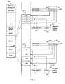
- FIG. 1is a block diagram of an example system 100 that includes a memory protection unit 102 that provides multiple alternative sets of memory protection attributes.
- the memory protection unit 102is shown in a microcontroller 103 that also includes an execution unit 104 and memory 107 .
- the microcontroller 103could be, for example, a member of the Atmel AVR32 family of microcontrollers.
- the memory protection unitcould be part of a memory device, a stand-alone controller device, or another device other than a microcontroller.
- various input/output resourcesare also provided (not shown in FIG. 1 ), and can be mapped to addresses within an overall memory map. In such implementations, use of input/output resources can also be controlled by the memory protection unit 102 .
- Memory 108is also included in the system 100 and is shown external to the microcontroller 103 .
- the memory 108is included in the same package as the microcontroller 103 .
- One or more buses 109can be used for memory and data transfers between the memory 108 and the microcontroller 103 .
- one bus 109 acan be used for instructions and another bus 109 b can be used for data.
- the execution unit 104can execute program instructions that are stored in the memory 108 . Execution of other program instructions can cause data to be retrieved from the memory 108 , manipulated in some manner by the execution unit 104 or stored in the memory 108 .
- the memory protection unit 102can be used to control the above-described operations.
- the memory protection unit 102can employ memory protection attributes to determine whether program instructions from a particular portion of memory 108 can be executed, or whether data can be read from or written to other portions of memory 108 .
- the memory protection unit 102can be employed to control whether data or instructions in various portions of memory 108 are bufferable or cacheable. For example, as shown in FIG.
- the data pathcan include one or more caches or buffers (e.g., instruction cache 124 , data cache 126 , instruction buffer 123 , data buffer 128 ) included in memory 107 , and the memory protection unit 102 can control whether data or instructions in various portions of memory 108 can be stored in or flow through one of the caches or buffers included in the memory 107 .
- caches or bufferse.g., instruction cache 124 , data cache 126 , instruction buffer 123 , data buffer 128 .
- attributes of different portions of memory 108can be applied to configurable regions or sub-regions of fixed or variable size that can be configurable through the memory protection unit 102 .
- the memory protection unit 102can include registers 110 , which can be configured to specify a location for each memory region or sub-region within a device's overall memory map.
- each regionhas a start address and size, based on values in a corresponding configuration register.
- each regionhas a start address and an ending address, which can be configured through a corresponding register or registers.
- each regionhas its own dedicated register or registers that characterize the region within the overall memory map.
- Each regioncan further include sub-regions.
- a fixed number of sub-regionse.g., three, four, eight, sixteen or some other number
- a fixed number of sub-regionsmay be distributed in a different manner.
- each regionmay include some sub-regions of a first size and other sub-regions of a second size.
- the number and distribution of sub-regions within a regioncan also be configurable through values in corresponding registers.
- registerscan store memory protection attributes that are applied to the various regions and sub-regions.
- one or more registerscan store values that specify whether particular regions or sub-regions are accessible for read, write or execution access (e.g., accessibility parameters).
- One or more other registerscan store values that specify whether contents of particular regions or sub-regions can be buffered (e.g., bufferability parameters).
- One or more other registerscan store values that specify whether contents of particular regions or sub-regions can be cached (e.g., cacheability parameters).
- the memory protection unit 102includes a first set of memory protection attributes (e.g., “A” attributes 130 ) and a second set of memory attributes (e.g., “B” attributes 132 ).
- Each set of memory protection attributes 130 or 132can include attributes that specify accessibility parameters for each region and sub-region, attributes that specify bufferability parameters for each region and sub-region, and attributes that specify cacheability parameters for each region and sub-region.
- other memory attributescan be included in each set.
- Implementations that include multiple alternative sets of memory protection attributescan include a mechanism for specifying which of the multiple alternative sets of memory protection attributes are to be applied to specific regions or sub-regions.
- some implementationsinclude a selection register (or a selection field within a register) for each sub-region of memory, which specifies which of the alternative sets of memory protection attributes are to be applied to the corresponding sub-region.
- the memory protection unitincludes one selection register for each region of memory, and each selection register includes a field for each sub-region within the region. Each field can store a value that uniquely identifies one of the alternative sets of memory protection attributes.
- the memory protection unit 102can be employed each time a memory access attempt or request is made (e.g., by the execution unit 104 executing program instructions). For example, if the execution unit 104 executes a read instruction directed to a specific address in instruction memory 114 , the memory protection unit 102 can identify a configured region and sub-region (e.g., a region or sub-region within the memory map that is characterized by values in the registers 110 ) that includes the specific address. The memory protection unit 102 can then determine which set of memory protection attributes (e.g., memory protection attributes 130 or 132 ) are to be applied to the relevant region and sub-region.
- memory protection attributese.g., memory protection attributes 130 or 132
- the memory protection unit 102can determine whether to allow or inhibit the memory access. In some implementations, the memory protection unit 102 inhibits a memory access by asserting an exception signal 134 that triggers an exception handler 112 within the execution unit 104 .
- a current mode of the execution unitis relevant in determining whether a memory access is to be permitted. For example, certain regions or sub-regions that are configured to cover the instruction memory 114 may only be accessible to the execution unit 104 when the execution unit is in a supervisory mode (e.g., as it may be when executing operating system instructions). Accordingly, the memory protection unit 102 may receive input from the execution unit 104 that specifies a current mode, which can, in some implementations, be used in conjunction with appropriate memory protection attributes in determining whether a memory access is to be allowed or inhibited.
- the system 100can include one or more caches (e.g., the data cache 126 or instruction cache 124 ) and one or more buffers (e.g., the instruction buffer 123 or the data buffer 128 ).
- the memory protection unit 102can also control whether data can be stored in or pass through a cache or buffer, or whether data is to bypass a cache and/or buffer.
- Some implementationsemploy caches and buffers to improve performance of a system, for example, where one or more aspects of a memory system are slower than the corresponding execution unit 104 .
- a fast cachee.g., data cache 126
- an instruction buffer 123can be employed to store multiple instructions retrieved from a relatively slow memory device, such as an instruction ROM.
- the memory protection unit 102can be employed to enforce buffer or cache parameters for particular regions or sub-regions of memory.
- FIG. 1depicts a Harvard architecture, in which instructions and data have separate data paths.
- a memory protection unitcan be employed within a von Neumann architecture, in which data and instructions travel over the same data path.
- the overall arrangement of componentscan be different.
- the memory protection unit 102can be included within the execution unit 104 .
- cache and bufferscan be included in the execution unit 104 in some implementations.
- bufferscan be included in individual memory devices.
- the memory protection unit 102can be a separate device that is external to the device that includes the execution unit 104 .
- cachecan be implemented by stand-alone devices, separate from the device that includes the execution unit 104 .
- more than one memory protection unitcan be provided.
- one memory protection unitcan be provided for the instruction path of a Harvard architecture-based device, and a second memory protection unit can be provided for the data path of the device.
- FIG. 1is a non-limiting example of one architecture, but various other architectures can be employed without departing from the spirit of this document.
- the memory system 107 and 108can include various kinds of memory devices, each of which can be used for different purposes (e.g., instructions, long-term data storage, scratch pad data storage, etc.), and each of which can have different specifications and operating parameters (e.g., width, size, speed, etc.).
- the example in FIG. 1depicts ROM, SRAM, DRAM and EEPROM devices.
- Other implementationscan include different kinds of memory (e.g., NVRAM, Flash, etc.) and different arrangements of the memory.
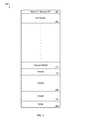
- FIG. 2is an example memory map 200 of the memory included in the system 100 shown in FIG. 1 .
- the memory map 200defines an address space for various memory types, including but not limited to: ROM 118 , SRAM 140 and 142 , DRAM 144 , internal SRAM 141 (e.g., internal registers), EEPROM 122 , and memory mapped I/O 202 .
- the memory map 200can be a map of a flat, unsegmented memory space controlled by memory protection unit 102 .
- ROM 118can be included in the instruction memory 114 .
- the ROM 118includes application program instructions that can be executed by the execution unit 104 .
- SRAM 140can also be included in instruction memory 114 .
- the SRAM 140includes application program instructions that may be separately loaded into the instruction memory 114 and used for a debugging mode or other type of special execution mode of the system 100 .
- SRAM 142 , DRAM 144 and EEPROM 122can be included in the data memory 108 .
- SRAM 142 and DRAM 144include data values used by application programs executed by the microcontroller 103 .
- EEPROM 122is used to store configuration values for a microcontroller based system.
- the EEPROM 122includes configuration values for peripheral devices included in the microcontroller based system. The use of EEPROM 122 to store configuration values can allow, for example, the values to be customized by a user for each system in which the microcontroller may be included.
- FIG. 3illustrates an example division of the memory 108 into regions that can include sub-regions, each of which can have different memory protection attributes.
- a protection region 302can be configured to include a portion of the ROM 118 , and the protection region 302 can include sub-regions 304 , 306 , 308 , and 310 .
- a memory protection unit address register 322(MPUAR 0 ) can be associated with region 302 . In one implementation, as shown, the address register 322 can be configured to define the start address and size of the protection region 302 .
- a second, memory protection unit address register 324(MPUAR 1 ) can define the start address and size of a second protection region 312 that, as shown, includes a portion of the DRAM 144 and has sub-regions 314 , 316 , 318 , and 320 .
- protection regionscan cover other areas of memory shown in the memory map 200 .
- the number of protection regions that can be included in the memory space of a microcontrollere.g., memory space mapped by the memory map 200
- a usermay program such configuration register(s) with a selected number of regions.
- the memory spaceis divided into eight regions.
- the memory spacecan be divided into sixteen or some other number of regions.
- FIG. 3illustrates two regions in the memory space mapped by memory map 200 .
- the protection regionscan be of different sizes.
- the size of each regionis characterized by a corresponding address register.
- the size of region 312can be specified by size bits 326 in address register 324 .
- the size of region 302can be specified by size bits 328 in address register 322 .
- memory regionscan be defined to cover the entire memory map 200 .
- memory regionsmay be defined that only cover a portion of the memory map 200 .
- the memory protection unit 102can optionally be configured to disable access to memory outside of defined protection regions (e.g., by causing an exception).
- all memoryis accessible, with unprotected regions being directly accessible, while memory protection attributes or protected regions are employed to enforce corresponding protection strategies.
- the address register associated with each regionincludes the base address for the start of the protection region in memory.
- the start in memory of region 312is specified by the base address 330 bits in address register 324 .
- the start of region 302is specified by the base address bits 332 in address register 322 .
- a regioncan range in size from 4 kBytes to 4 GBytes.
- the size of the regioncan be a power of two.
- the start address of the region(the base address) can be an integer multiple of the region size. For example, if the region is 8 kBytes, the 13 lowest bits of the start address may be implicitly set to zero.
- the size of a regioncan be specified by providing an end address for the region which can be included in an additional address register, for example, that can be associated with the region.
- the base addressneed not be an integer multiple of the region size.
- each address registeralso includes a valid bit (e.g., valid bits 323 and 325 ).
- the valid bitcan specify if the protection region is valid.
- memory protection attributesare only applied to valid regions. If a region is not valid, no memory accesses may be deemed to map to the region.
- each regioncan be divided into a number of sub-regions.
- region 312includes four sub-regions 314 , 316 , 318 , and 320 .
- the number of sub-regions included in a regioncan be another number that may be a power of two, which may divide the region into equal portions.
- the size of region 312is 8 kBytes. Since region 312 includes four sub-regions 314 , 316 , 318 , and 320 , each sub-region's size is equal to 2 kBytes in this example.
- a regioncan include eight or sixteen sub-regions, or some other number that may or may not be a power of two.
- each regionhas associated with it a select register, whose contents specify which set of multiple alternative sets of memory protection attributes are to be applied to the region or to sub-regions within the region.
- region 312has associated with it memory protection unit permission select register 334 (MPUPSR 1 ) and region 302 has associated with it memory protection unit permission select register 336 (MPUPSR 0 ).
- Each select registercan be divided into n fields that correspond to n sub-regions of the region, for example, to provide additional granularity in memory attribute configurability.
- Each fieldcan specify which of multiple alternative sets of memory protection attributes are to be applied to a corresponding sub-region.
- select register 334includes four fields— 337 , 338 , 340 , and 342 —which correspond to sub-regions 320 , 318 , 316 , 314 , respectively.
- each fieldspecifies whether the “A” alternative set of memory protection attributes are to be applied to the corresponding sub-region, or whether the “B” set of memory protection attributes are to be applied to the corresponding sub-region.
- field 337specifies that “A” attributes are to be applied to sub-region 320 ; field 338 specifies that “B” attributes are to be applied to sub-region 318 ; and so on.
- each regionhas its own select registers, a specific set of alternative memory protection attributes can be individually assigned to each sub-region, within each region in the memory map, providing in these implementations, considerable flexibility in memory protection.
- a select registerincludes eight fields for eight sub-regions. In other implementations, a select register includes sixteen fields for sixteen sub-regions. In some implementations, each field of the select register can include multiple bits to allow more sets of properties to be supported. For example, if the fields in the register 334 or 336 included two bits, four sets of memory property registers could be supported. In some implementations, additional memory properties can be supported with the inclusion of additional memory property registers for each register set supported by the specific implementation. In the example of FIG. 3 , each region is divided into the same number of sub-regions. In other implementations, each region may be divided into a different number of sub-regions.
- FIG. 4is a diagram of example registers that can be associated with the various regions and sub-regions that are shown in FIG. 3 .
- FIG. 4illustrates sample memory protection unit cacheability registers 402 a (MPUCRA) and 402 b (MPUCRB) that can specify alternative cacheability parameters for each region (e.g., fields 404 a and 416 a can specify alternative cacheability parameters for the first region 302 ; fields 405 a and 417 a can specify alternative cacheability parameters for the second region 312 ; etc.); sample memory protection unit bufferability registers 406 a (MPUBRA) and 406 b MPUBRB) that can specify alternative bufferability parameters for each region; and sample memory protection unit access permission registers 410 a (MPUAPRA) and 410 b (MPUAPRB) that can specify alternative access permissions for each region.
- MPUCRAsample memory protection unit cacheability registers 402 a
- MPUCRBsample memory protection unit cacheability registers 402 a
- MPUCRBsample memory protection
- the sample cacheability register 402 a , bufferable register 406 a , and the access permission register 410 amake up a first set of alternative memory protection parameters (e.g., the “A” register set 130 , as shown in FIG. 1 ).
- a second alternative set of memory protection parameters(e.g., the “B” register set 132 , as shown in FIG. 1 ) can include a second memory protection unit cacheable register 402 b (MPUCRB), a second memory protection unit bufferable register 406 b (MPUBRB), and a second memory protection unit access permission register 410 b (MPUAPRB). Additional alternative sets of memory protection attributes can be included but are not shown in FIG. 4 .
- a select register(e.g., the select register 336 ) can be used to select which of the alternative sets of memory protection attributes are to be applied to a specific sub-region within the region corresponding to the select register.
- the select register 336includes four fields: 344 , 346 , 348 , 350 —each of which is associated with sub-regions 310 , 308 , 306 , and 304 , respectively.
- field 348the third field of select register 336 , can specify that memory parameters in the “A” register set 130 are to be applied to the third sub-region 306 of the first region (e.g., rather than memory protection parameters from register set “B”).
- cacheability parameters from the “A” register set 130e.g., from the register 402 a
- bufferability parameters from the “A” register set 130e.g., from the register 406 a
- access permission parameters from the “A” register set 130e.g., from the register 410 a
- each of the parameter registersare themselves divided into as many fields as there are regions.
- the particular field that supplies a memory parameter for a particular regioncorresponds to the number of the particular region. That is, in a cacheability register having four fields, the third field supplies cacheability parameters for the third region; the second field supplies cacheability parameters for the second region; and so on.
- the cacheability register 402 aincludes four fields, one field for each region.
- the first field in the cacheability register 402 a , field 404 acan specify a first alternative cacheability parameter for region 302 .
- a field 404 a value equal to “1”can specify, for example, that, when the “A” set of parameters is selected for a given sub-region, the region 302 (in particular, the corresponding sub-region of region 302 ) is cacheable.
- Bufferability register 406 aalso includes four fields, one field for each region. The first field in the bufferability register 406 a , field 404 b , can specify a first alternative bufferability parameter of region 302 .
- a field 404 b value equal to “0”can specify, for example, that, when the “A” set of parameters is selected for a given sub-region, the region 302 (in particular, the corresponding sub-region of region 302 ) is not bufferable.
- Access permission register 410 aalso includes four fields, one field for each region.
- the first field in the access permission register 410 a , field 404 ccan specify a first alternative set of access permissions of region 302 .
- a field 404 c value equal to “0100”can specify, for example, that, when the “A” set of parameters is selected for a given sub-region, the region 302 (in particular, the corresponding sub-region of region 302 ) is read-only.
- a second set of alternative memory parameterscan be provided by cacheability register 402 b , bufferability register 406 b and access permission register 410 b .
- the first fields of these registers, 416 a , 416 b and 416 ccan respectively specify second alternative cacheability, bufferability and access permission parameters for the first region 302 .
- a field in the first region's select registere.g., MPUPSR 0 336 ) can select which set of alternative parameters are to be applied to a corresponding sub-region.
- field 344specifies that “B” memory parameters (e.g., parameters specified by fields 416 a , 416 b and 416 c ) are to be applied to the first sub-region of the first region; as another example, field 348 specifies that “A” memory parameters (e.g., parameters specified by fields 404 a , 404 b and 404 c ) are to be applied to the third sub-region of the first region.
- “B” memory parameterse.g., parameters specified by fields 416 a , 416 b and 416 c
- field 348specifies that “A” memory parameters (e.g., parameters specified by fields 404 a , 404 b and 404 c ) are to be applied to the third sub-region of the first region.
- the above-described arrangement and scheme for decoding memory parametersprovides considerable flexibility in configuring memory protection.
- the value of an access permission fieldcan specify different access permissions, depending on a privilege mode associated with the execution unit. For example, with reference to the table of example encoded values for other access permission modes, shown below, a value of “0001” can specify read and execute access to a region when the execution unit is in a supervisory mode; but the same value can specify no access if the execution unit is in a normal mode. Other values are provided in the table below as non-limiting examples of various combinations of access permissions that can be stored in the access permission registers 410 a and 410 b .
- Permission in Permission in privileged mode non-privileged modeEncoded value (e.g., supervisory mode) (e.g., normal mode) 0000 Read None 0001 Read/Execute None 0010 Read/Write None 0011 Read/Write/Execute None 0100 Read Read 0101 Read/Execute Read/Execute 0110 Read/Write Read/Write 0111 Read/Write/Execute Read/Write/Execute 1000 Read/Write Read 1001 Read/Write Read/Execute 1010 None None Other UNDEFINED UNDEFINED
- FIG. 5Ais a diagram of example aggregate memory parameters (e.g., access, bufferability and cacheability parameters) for the “A” register set 130 based on example bit encodings for each field of the corresponding registers.
- example parameters that are encoded by the fields of the cacheability register 402 a , the bufferable register 406 a , and the access permission register 410 aare depicted in FIG. 5A .
- the memory parameters 508which correspond to the first region 302 , are specified in this example by corresponding first fields 404 a , 404 b and 404 c in the cacheability, bufferability and access permission registers, respectively.
- FIG. 5Bis a diagram of example aggregate memory parameters for the “B” register set 132 .
- memory parameters 516are specified by fields 416 a , 416 b and 416 c . These fields also specify memory parameters for the first region 302 , but for the “B” register set. Thus, the memory 516 parameters would be active in a sub-region of the first region whose select register field specifies the “B” set of memory parameters (e.g., as depicted in FIG. 4 , the first and second sub-regions, as specified by fields 344 and 346 ).
- each regioncan have its own select register (such as the select register 336 , corresponding to region 0 ); thus, considerable flexibility is possible within the above-described memory protection scheme. Moreover, some implementations support more than two sets of alternative memory protection parameters (e.g, by increasing the number of bits in various fields of the registers), thereby providing additional flexibility.
- FIG. 6is a block diagram showing additional details of an example memory protection unit.
- the execution unit 104shown in FIG. 1 , can generate an address (ADDR 602 ).
- a region hit check module 604can identify the region and sub-region to which the memory access of address ADDR 602 maps. This can be determined, for example, by comparing the address to each of the address registers. More specifically, the address can be compared to a starting address and size in each address register to determine which region the address maps to.
- the region hit check module 604can identify the sub-region.
- a “multi” exception signal 608can be asserted and the memory access may be aborted or inhibited.
- a priority schemecan be applied to select one of multiple overlapping regions to which a generated address maps. If the address maps to no region, a “none” exception signal 606 can be asserted, in some implementations, and the memory access may not be performed. In particular, for example, the exception signal can be sent to the exception handler 112 to be handled by the execution unit 104 . In other implementations, accesses to memory regions that are not protected may simply be allowed to proceed.
- the memory protection unit 102can identify and enforce memory protection parameters associated with the identified sub-region.
- a select register that corresponds to the identified regione.g., the first select register, MPUPSR 0 336
- MPUPSR 0 336can be used to identify which of the alternative sets of memory protection attributes are to be applied to the sub-region of memory being accessed.
- a field within the select register(e.g., the third field) that corresponds to the position of the identified sub-region (e.g., the third sub-region) can be used to identify which of the alternative sets of memory protection attributes are to be applied.
- the third field of the select register 336(field 348 ) specifies the “A” set of alternative memory protection attributes (e.g., attributes 508 specified by fields 404 a , 404 b and 404 c ). As depicted in one implementation in FIG. 6 , this field can be used to control a multiplexer 610 that can route the appropriate set of alternative memory protection attributes to a privilege check module 616 .
- the privilege check module 616can apply the alternative memory protection attributes provided to it in order to determine whether to allow or inhibit the memory attempted memory access. For example, the privilege check module 616 can issue various control signals and exception signals to enforce a memory protection scheme. In particular, as one example, the privilege check module 616 can assert an instruction protection exception signal (“iprot” 624 ) if an attempted access to instruction memory violates the relevant protection scheme, and the privilege check module 616 can assert a similar data protection exception signal (“dprot” 626 ) if an attempted access to data memory violates the relevant protection scheme. In some implementations, such exception signals can be routed to an exception handler, such as the exception handler 112 that is shown in FIG. 1 .
- an exception handlersuch as the exception handler 112 that is shown in FIG. 1 .
- the privilege check module 616can assert control signals to enable or disable instruction or data caches (“icach” 628 and “dcach” 630 , respectively) or to enable or disable instruction or data buffers (“ibuf” 631 and “dbuf” 632 , respectively).
- the privilege check module 616includes additional inputs which can be used in enforcing a memory protection policy.
- the privilege check module 616can receive a signal 618 that indicates whether the execution unit is in a privileged or supervisory mode, a signal 620 that indicates whether the attempted memory access is a write or a read, and a signal 622 that indicates whether memory access is directed to instruction or data memory (e.g., in a Harvard-architecture device).
- a memory protection unitcan include two or more channels (e.g., one for instruction fetches and one for data access).
- the channelscan be implemented by two separate memory protection units; in other implementations, the two channels can be implemented by a single memory protection unit.
- FIG. 7is a flow diagram of an example method 700 for enforcing memory protection parameters for a sub-region in memory.
- the method 700can start, for example, when the execution unit 104 generates a request for a memory access at a specific address (ADDR) (box 702 ).
- a memory protection unit control register(not shown in the previous figures) can be checked to determine whether memory protection is enabled (box 704 ). If memory protection (e.g., address checking) is disabled, the method 700 can end; and if address checking is enabled, the method 700 continues.
- a region in memorycan be identified based on the address value, ADDR (box 706 ).
- the region hit check module 604shown in FIG. 6 , can identify which region and sub-region the memory access at ADDR 602 maps to (boxes 706 and 708 ) using the values in the address registers.
- the region hit check module 604can determine, in box 710 , if the address maps to a valid region (e.g., to exactly one region, in some implementations).
- exception signalscan be asserted ( 711 ) to the exception handler 112 , causing, in one implementation as shown, the access to be aborted or inhibiting, and causing the method 700 to end; if the address is valid, the method 700 can continue.
- Appropriate memory protection attributescan be identified.
- an appropriate set of alternative memory protection attributescan be identified, and specific protection attributes within the set can be obtained (e.g., based on value(s) in an appropriate selection register), and other values in appropriate fields of corresponding cacheability, bufferability and access permission registers can be obtained (box 712 ).
- a region to which the address mapscan be associated with a select register (e.g., register 336 ).
- the field in the select register corresponding to the sub-region to which the address mapscan specify the appropriate alternative set of memory parameters (e.g., the “A” register set 130 or the “B” register set 132 ), from which specific memory properties for the sub-region can be drawn.
- the memory properties for the sub-regioncan be provided by fields in the various corresponding memory protection registers (e.g., a cacheability register, a bufferability register and an access permissions register) that correspond to the region.
- the privilege check module 616can then determine (box 722 ) whether the attempted access is allowed by the implemented memory protection policy. If so, the memory access can be allowed (box 724 ). If the attempted access is not allowed by the implemented memory protection policy, the memory access can be blocked or inhibited, and the memory protection unit may additionally generate an exception (box 726 ).
- the current microcontroller privilege levelis relevant to determining whether an attempted access is allowed. Whether the memory access is an attempted write or an attempted read, and whether the access is directed to instruction or data memory may also be relevant to determining whether an attempted access is allowed. If any of privilege, access type or access target (e.g., data memory or instruction memory) are relevant to a memory protection scheme, this information can also be identified (identification not shown in FIG. 7 ).
Landscapes
- Engineering & Computer Science (AREA)
- Theoretical Computer Science (AREA)
- Computer Security & Cryptography (AREA)
- Physics & Mathematics (AREA)
- General Engineering & Computer Science (AREA)
- General Physics & Mathematics (AREA)
- Storage Device Security (AREA)
Abstract
Description
| Permission in | Permission in | ||
| privileged mode | non-privileged mode | ||
| Encoded value | (e.g., supervisory mode) | (e.g., normal mode) | |
| 0000 | Read | None | |
| 0001 | Read/Execute | ||
| 0010 | Read/Write | None | |
| 0011 | Read/Write/Execute | ||
| 0100 | Read | ||
| 0101 | Read/Execute | Read/Execute | |
| 0110 | Read/Write | Read/ | |
| 0111 | Read/Write/Execute | Read/Write/Execute | |
| 1000 | Read/ | Read | |
| 1001 | Read/Write | Read/Execute | |
| 1010 | None | None | |
| Other | UNDEFINED | UNDEFINED | |
Claims (12)
Priority Applications (3)
| Application Number | Priority Date | Filing Date | Title |
|---|---|---|---|
| US11/744,573US8051263B2 (en) | 2007-05-04 | 2007-05-04 | Configurable memory protection |
| PCT/US2008/061175WO2008137316A1 (en) | 2007-05-04 | 2008-04-22 | Configurable memory protection |
| TW097116389ATW200903255A (en) | 2007-05-04 | 2008-05-02 | Configurable memory protection |
Applications Claiming Priority (1)
| Application Number | Priority Date | Filing Date | Title |
|---|---|---|---|
| US11/744,573US8051263B2 (en) | 2007-05-04 | 2007-05-04 | Configurable memory protection |
Publications (2)
| Publication Number | Publication Date |
|---|---|
| US20080276051A1 US20080276051A1 (en) | 2008-11-06 |
| US8051263B2true US8051263B2 (en) | 2011-11-01 |
Family
ID=39580136
Family Applications (1)
| Application Number | Title | Priority Date | Filing Date |
|---|---|---|---|
| US11/744,573Active2029-01-18US8051263B2 (en) | 2007-05-04 | 2007-05-04 | Configurable memory protection |
Country Status (3)
| Country | Link |
|---|---|
| US (1) | US8051263B2 (en) |
| TW (1) | TW200903255A (en) |
| WO (1) | WO2008137316A1 (en) |
Cited By (6)
| Publication number | Priority date | Publication date | Assignee | Title |
|---|---|---|---|---|
| US9430409B2 (en) | 2012-06-27 | 2016-08-30 | Nordic Semiconductor Asa | Memory protection |
| WO2017163204A1 (en)* | 2016-03-23 | 2017-09-28 | Craig Michael Horn | A memory management system and method |
| US20180343234A1 (en)* | 2017-05-26 | 2018-11-29 | Microsoft Technology Licensing, Llc | Subsystem firewalls |
| US10346345B2 (en) | 2017-05-26 | 2019-07-09 | Microsoft Technology Licensing, Llc | Core mapping |
| US10353815B2 (en) | 2017-05-26 | 2019-07-16 | Microsoft Technology Licensing, Llc | Data security for multiple banks of memory |
| US10659455B2 (en) | 2014-04-09 | 2020-05-19 | Cardex Systems Inc. | Self-authenticating chips |
Families Citing this family (35)
| Publication number | Priority date | Publication date | Assignee | Title |
|---|---|---|---|---|
| TW200805065A (en)* | 2006-01-17 | 2008-01-16 | Nxp Bv | Region protection unit, instruction set and method for protecting a memory region |
| JP4939387B2 (en) | 2007-12-06 | 2012-05-23 | ルネサスエレクトロニクス株式会社 | Data processing apparatus and address space protection method |
| US8301856B2 (en)* | 2010-02-16 | 2012-10-30 | Arm Limited | Restricting memory areas for an instruction read in dependence upon a hardware mode and a security flag |
| EP2383654A1 (en)* | 2010-04-28 | 2011-11-02 | Siemens Aktiengesellschaft | A memory device and a firmware configurator |
| US20130111181A1 (en)* | 2011-10-31 | 2013-05-02 | Lsi Corporation | Methods and apparatus for increasing device access performance in data processing systems |
| KR20130050156A (en)* | 2011-11-07 | 2013-05-15 | 한국전자통신연구원 | Apparatus for translating virtual address space |
| CN108959110B (en) | 2011-12-29 | 2023-05-30 | 太浩研究有限公司 | Processor for preventing administrator mode execution of user mode instructions and method thereof |
| US9495305B1 (en) | 2012-11-02 | 2016-11-15 | David Fuchs | Detecting pointer errors for memory protection |
| US9720843B2 (en)* | 2012-12-28 | 2017-08-01 | Intel Corporation | Access type protection of memory reserved for use by processor logic |
| US9317426B2 (en) | 2013-01-08 | 2016-04-19 | GreenTec-USA. Inc. | Write once read many media methods |
| US9395993B2 (en)* | 2013-07-29 | 2016-07-19 | Intel Corporation | Execution-aware memory protection |
| US9513692B2 (en)* | 2013-09-18 | 2016-12-06 | Intel Corporation | Heterogenous memory access |
| US9411600B2 (en)* | 2013-12-08 | 2016-08-09 | Intel Corporation | Instructions and logic to provide memory access key protection functionality |
| US9307409B2 (en) | 2013-12-27 | 2016-04-05 | Intel Corporation | Apparatus, system and method of protecting domains of a multimode wireless radio transceiver |
| GB2522906B (en)* | 2014-02-10 | 2021-07-14 | Advanced Risc Mach Ltd | Region identifying operation for identifying a region of a memory attribute unit corresponding to a target memory address |
| US9710404B2 (en)* | 2015-03-23 | 2017-07-18 | Intel Corporation | Dynamic configuration and peripheral access in a processor |
| US10114958B2 (en)* | 2015-06-16 | 2018-10-30 | Microsoft Technology Licensing, Llc | Protected regions |
| JP6504984B2 (en)* | 2015-09-28 | 2019-04-24 | ルネサスエレクトロニクス株式会社 | Data processor |
| US20170139844A1 (en)* | 2015-11-17 | 2017-05-18 | Silicon Laboratories Inc. | Asymmetric memory |
| US10824572B2 (en) | 2016-09-09 | 2020-11-03 | Cylance Inc. | Memory space protection |
| DE102016220639A1 (en)* | 2016-10-20 | 2018-04-26 | Infineon Technologies Ag | Memory protection unit and method for protecting a memory address space |
| US10671547B2 (en) | 2016-12-19 | 2020-06-02 | Intel Corporation | Lightweight trusted tasks |
| US11500665B2 (en) | 2018-08-30 | 2022-11-15 | Micron Technology, Inc. | Dynamic configuration of a computer processor based on the presence of a hypervisor |
| US10942863B2 (en) | 2018-08-30 | 2021-03-09 | Micron Technology, Inc. | Security configurations in page table entries for execution domains using a sandbox application operation |
| US11914726B2 (en) | 2018-08-30 | 2024-02-27 | Micron Technology, Inc. | Access control for processor registers based on execution domains |
| US11481241B2 (en) | 2018-08-30 | 2022-10-25 | Micron Technology, Inc. | Virtual machine register in a computer processor |
| US10915457B2 (en) | 2018-08-30 | 2021-02-09 | Micron Technology, Inc. | Memory access control through permissions specified in page table entries for execution domains |
| US11182507B2 (en) | 2018-08-30 | 2021-11-23 | Micron Technology, Inc. | Domain crossing in executing instructions in computer processors |
| US10915465B2 (en) | 2018-08-30 | 2021-02-09 | Micron Technology, Inc. | Memory configured to store predefined set of domain registers for instructions being executed in computer processors |
| US11256427B2 (en)* | 2018-12-28 | 2022-02-22 | Micron Technology, Inc. | Unauthorized memory access mitigation |
| US11256631B1 (en)* | 2020-01-17 | 2022-02-22 | Ralph Crittenden Moore | Enhanced security via dynamic regions for memory protection units (MPUs) |
| GB2593506B (en)* | 2020-03-25 | 2022-05-11 | Advanced Risc Mach Ltd | Memory system verification |
| US20230350805A1 (en)* | 2022-04-29 | 2023-11-02 | Cadence Design Systems, Inc. | Technique for Overriding Memory Attributes |
| US20250021494A1 (en)* | 2023-07-13 | 2025-01-16 | Texas Instruments Incorporated | Processor with hardware-integrated memory access protection |
| FR3155620A1 (en)* | 2023-11-17 | 2025-05-23 | Stmicroelectronics International N.V. | Method of operating a non-volatile memory |
Citations (14)
| Publication number | Priority date | Publication date | Assignee | Title |
|---|---|---|---|---|
| US5325499A (en) | 1990-09-28 | 1994-06-28 | Tandon Corporation | Computer system including a write protection circuit for preventing illegal write operations and a write poster with improved memory |
| US5649159A (en)* | 1994-08-31 | 1997-07-15 | Motorola, Inc. | Data processor with a multi-level protection mechanism, multi-level protection circuit, and method therefor |
| US6021476A (en)* | 1997-04-30 | 2000-02-01 | Arm Limited | Data processing apparatus and method for controlling access to a memory having a plurality of memory locations for storing data values |
| US6484227B1 (en) | 1999-08-23 | 2002-11-19 | Advanced Micro Devices, Inc. | Method and apparatus for overlapping programmable address regions |
| US6519690B1 (en)* | 1999-08-23 | 2003-02-11 | Advanced Micro Devices, Inc. | Flexible address programming with wrap blocking |
| US20030101322A1 (en) | 2001-10-25 | 2003-05-29 | Gardner Robert D. | Protection of user process data in a secure platform architecture |
| US6697276B1 (en) | 2002-02-01 | 2004-02-24 | Netlogic Microsystems, Inc. | Content addressable memory device |
| WO2004046934A2 (en) | 2002-11-18 | 2004-06-03 | Arm Limited | Secure memory for protecting against malicious programs |
| US6901505B2 (en) | 2001-08-09 | 2005-05-31 | Advanced Micro Devices, Inc. | Instruction causing swap of base address from segment register with address from another register |
| US6904504B2 (en)* | 2001-11-14 | 2005-06-07 | Intel Corporation | Method and apparatus for software selection of protected register settings |
| US20050268058A1 (en)* | 2004-05-27 | 2005-12-01 | Microsoft Corporation | Alternative methods in memory protection |
| US7068545B1 (en)* | 2005-01-04 | 2006-06-27 | Arm Limited | Data processing apparatus having memory protection unit |
| US20070011419A1 (en)* | 2005-07-07 | 2007-01-11 | Conti Gregory R | Method and system for a multi-sharing security firewall |
| US20070250675A1 (en)* | 2006-04-20 | 2007-10-25 | Nec Electronics Corporation | Microcomputer and method for controlling memory access |
- 2007
- 2007-05-04USUS11/744,573patent/US8051263B2/enactiveActive
- 2008
- 2008-04-22WOPCT/US2008/061175patent/WO2008137316A1/enactiveApplication Filing
- 2008-05-02TWTW097116389Apatent/TW200903255A/enunknown
Patent Citations (14)
| Publication number | Priority date | Publication date | Assignee | Title |
|---|---|---|---|---|
| US5325499A (en) | 1990-09-28 | 1994-06-28 | Tandon Corporation | Computer system including a write protection circuit for preventing illegal write operations and a write poster with improved memory |
| US5649159A (en)* | 1994-08-31 | 1997-07-15 | Motorola, Inc. | Data processor with a multi-level protection mechanism, multi-level protection circuit, and method therefor |
| US6021476A (en)* | 1997-04-30 | 2000-02-01 | Arm Limited | Data processing apparatus and method for controlling access to a memory having a plurality of memory locations for storing data values |
| US6484227B1 (en) | 1999-08-23 | 2002-11-19 | Advanced Micro Devices, Inc. | Method and apparatus for overlapping programmable address regions |
| US6519690B1 (en)* | 1999-08-23 | 2003-02-11 | Advanced Micro Devices, Inc. | Flexible address programming with wrap blocking |
| US6901505B2 (en) | 2001-08-09 | 2005-05-31 | Advanced Micro Devices, Inc. | Instruction causing swap of base address from segment register with address from another register |
| US20030101322A1 (en) | 2001-10-25 | 2003-05-29 | Gardner Robert D. | Protection of user process data in a secure platform architecture |
| US6904504B2 (en)* | 2001-11-14 | 2005-06-07 | Intel Corporation | Method and apparatus for software selection of protected register settings |
| US6697276B1 (en) | 2002-02-01 | 2004-02-24 | Netlogic Microsystems, Inc. | Content addressable memory device |
| WO2004046934A2 (en) | 2002-11-18 | 2004-06-03 | Arm Limited | Secure memory for protecting against malicious programs |
| US20050268058A1 (en)* | 2004-05-27 | 2005-12-01 | Microsoft Corporation | Alternative methods in memory protection |
| US7068545B1 (en)* | 2005-01-04 | 2006-06-27 | Arm Limited | Data processing apparatus having memory protection unit |
| US20070011419A1 (en)* | 2005-07-07 | 2007-01-11 | Conti Gregory R | Method and system for a multi-sharing security firewall |
| US20070250675A1 (en)* | 2006-04-20 | 2007-10-25 | Nec Electronics Corporation | Microcomputer and method for controlling memory access |
Non-Patent Citations (6)
| Title |
|---|
| "AVR101: High Endurance EEPROM", ARM1156T2F-S Technical Reference Manual Rev.RUpl, ARM Ltd., , Chapter 3 pp. 61-60 and Chapter 5 p. 7.* |
| "AVR101: High Endurance EEPROM", ARM1156T2F-S Technical Reference Manual Rev.RUpl, ARM Ltd., <www.arm.com/pdfs/DDI0290C—arm1156t2fs—r0p0—trm.pdf>, Chapter 3 pp. 61-60 and Chapter 5 p. 7.* |
| "Introduction to the Cortex-M3 Processor," white paper available at http://www.arm.com/pdfs/IntroToCortex-M3.pdf, 17 pages, Oct. 2006. |
| ARM Cortex-M3 Datasheet, available at http://www.arm.com/pdfs/Cortex-M3-DS.pdf, 4 pages, Jan. 2003. |
| International Search Report & Written Opinion, PCT/US/2008/061175, mailed Jul. 30, 2008, 12 pages. |
| TMS470R1x System Module Reference Guide, available at http://focus.ti.com/lit/ug/spnu189h/spnu189h.pdf, 132 pages, Nov. 2004. |
Cited By (12)
| Publication number | Priority date | Publication date | Assignee | Title |
|---|---|---|---|---|
| US9430409B2 (en) | 2012-06-27 | 2016-08-30 | Nordic Semiconductor Asa | Memory protection |
| EP3702923A1 (en) | 2012-06-27 | 2020-09-02 | Nordic Semiconductor ASA | Memory protection |
| US10659455B2 (en) | 2014-04-09 | 2020-05-19 | Cardex Systems Inc. | Self-authenticating chips |
| US11336642B2 (en) | 2014-04-09 | 2022-05-17 | Cardex Systems Inc. | Self-authenticating chips |
| US12021863B2 (en) | 2014-04-09 | 2024-06-25 | Cardex Systems Inc. | Self-authenticating chips |
| WO2017163204A1 (en)* | 2016-03-23 | 2017-09-28 | Craig Michael Horn | A memory management system and method |
| US20180343234A1 (en)* | 2017-05-26 | 2018-11-29 | Microsoft Technology Licensing, Llc | Subsystem firewalls |
| US10346345B2 (en) | 2017-05-26 | 2019-07-09 | Microsoft Technology Licensing, Llc | Core mapping |
| US10353815B2 (en) | 2017-05-26 | 2019-07-16 | Microsoft Technology Licensing, Llc | Data security for multiple banks of memory |
| US10587575B2 (en)* | 2017-05-26 | 2020-03-10 | Microsoft Technology Licensing, Llc | Subsystem firewalls |
| US10783075B2 (en) | 2017-05-26 | 2020-09-22 | Microsoft Technology Licensing, Llc | Data security for multiple banks of memory |
| US11444918B2 (en)* | 2017-05-26 | 2022-09-13 | Microsoft Technology Licensing, Llc | Subsystem firewalls |
Also Published As
| Publication number | Publication date |
|---|---|
| US20080276051A1 (en) | 2008-11-06 |
| TW200903255A (en) | 2009-01-16 |
| WO2008137316A1 (en) | 2008-11-13 |
Similar Documents
| Publication | Publication Date | Title |
|---|---|---|
| US8051263B2 (en) | Configurable memory protection | |
| US8949551B2 (en) | Memory protection unit (MPU) having a shared portion and method of operation | |
| TWI797347B (en) | Apparatus, method and computer program with memory protection unit using memory protection table stored in memory system to control access to memory | |
| JP7449273B2 (en) | Range check command | |
| US8352694B2 (en) | Method of controlling memory access | |
| JP6652491B2 (en) | Area specifying operation for specifying the area of the memory attribute unit corresponding to the target memory address | |
| US9430409B2 (en) | Memory protection | |
| US9116845B2 (en) | Remote permissions provisioning for storage in a cache and device therefor | |
| US8639895B2 (en) | Systems and methods for memory region descriptor attribute override | |
| US20180095902A1 (en) | Enforcing memory operand types using protection keys | |
| US20130254491A1 (en) | Controlling a processor cache using a real-time attribute | |
| KR102817483B1 (en) | Binary search procedure for control tables stored in the memory system. | |
| US20120215989A1 (en) | Memory protection in a data processing system | |
| KR20180033467A (en) | Processor with advanced operating system support | |
| JP6071341B2 (en) | Memory management unit with region descriptor globalization control | |
| GB2440968A (en) | Protecting system control registers in a data processing apparatus | |
| US7716453B2 (en) | Descriptor-based memory management unit and method for memory management | |
| US20230409494A1 (en) | Technique for constraining access to memory using capabilities | |
| US11119941B2 (en) | Capability enforcement controller | |
| US12007902B2 (en) | Configurable memory system and memory managing method thereof | |
| KR20230058678A (en) | Memory protection for vector operations |
Legal Events
| Date | Code | Title | Description |
|---|---|---|---|
| AS | Assignment | Owner name:ATMEL CORPORATION, CALIFORNIA Free format text:ASSIGNMENT OF ASSIGNORS INTEREST;ASSIGNOR:RENNO, ERIK KNUTSEN;REEL/FRAME:019362/0955 Effective date:20070503 | |
| STCF | Information on status: patent grant | Free format text:PATENTED CASE | |
| AS | Assignment | Owner name:MORGAN STANLEY SENIOR FUNDING, INC. AS ADMINISTRATIVE AGENT, NEW YORK Free format text:PATENT SECURITY AGREEMENT;ASSIGNOR:ATMEL CORPORATION;REEL/FRAME:031912/0173 Effective date:20131206 Owner name:MORGAN STANLEY SENIOR FUNDING, INC. AS ADMINISTRAT Free format text:PATENT SECURITY AGREEMENT;ASSIGNOR:ATMEL CORPORATION;REEL/FRAME:031912/0173 Effective date:20131206 | |
| CC | Certificate of correction | ||
| FPAY | Fee payment | Year of fee payment:4 | |
| AS | Assignment | Owner name:ATMEL CORPORATION, CALIFORNIA Free format text:TERMINATION AND RELEASE OF SECURITY INTEREST IN PATENT COLLATERAL;ASSIGNOR:MORGAN STANLEY SENIOR FUNDING, INC.;REEL/FRAME:038376/0001 Effective date:20160404 | |
| AS | Assignment | Owner name:JPMORGAN CHASE BANK, N.A., AS ADMINISTRATIVE AGENT, ILLINOIS Free format text:SECURITY INTEREST;ASSIGNOR:ATMEL CORPORATION;REEL/FRAME:041715/0747 Effective date:20170208 Owner name:JPMORGAN CHASE BANK, N.A., AS ADMINISTRATIVE AGENT Free format text:SECURITY INTEREST;ASSIGNOR:ATMEL CORPORATION;REEL/FRAME:041715/0747 Effective date:20170208 | |
| AS | Assignment | Owner name:JPMORGAN CHASE BANK, N.A., AS ADMINISTRATIVE AGENT, ILLINOIS Free format text:SECURITY INTEREST;ASSIGNORS:MICROCHIP TECHNOLOGY INCORPORATED;SILICON STORAGE TECHNOLOGY, INC.;ATMEL CORPORATION;AND OTHERS;REEL/FRAME:046426/0001 Effective date:20180529 Owner name:JPMORGAN CHASE BANK, N.A., AS ADMINISTRATIVE AGENT Free format text:SECURITY INTEREST;ASSIGNORS:MICROCHIP TECHNOLOGY INCORPORATED;SILICON STORAGE TECHNOLOGY, INC.;ATMEL CORPORATION;AND OTHERS;REEL/FRAME:046426/0001 Effective date:20180529 | |
| AS | Assignment | Owner name:WELLS FARGO BANK, NATIONAL ASSOCIATION, AS NOTES COLLATERAL AGENT, CALIFORNIA Free format text:SECURITY INTEREST;ASSIGNORS:MICROCHIP TECHNOLOGY INCORPORATED;SILICON STORAGE TECHNOLOGY, INC.;ATMEL CORPORATION;AND OTHERS;REEL/FRAME:047103/0206 Effective date:20180914 Owner name:WELLS FARGO BANK, NATIONAL ASSOCIATION, AS NOTES C Free format text:SECURITY INTEREST;ASSIGNORS:MICROCHIP TECHNOLOGY INCORPORATED;SILICON STORAGE TECHNOLOGY, INC.;ATMEL CORPORATION;AND OTHERS;REEL/FRAME:047103/0206 Effective date:20180914 | |
| MAFP | Maintenance fee payment | Free format text:PAYMENT OF MAINTENANCE FEE, 8TH YEAR, LARGE ENTITY (ORIGINAL EVENT CODE: M1552); ENTITY STATUS OF PATENT OWNER: LARGE ENTITY Year of fee payment:8 | |
| AS | Assignment | Owner name:JPMORGAN CHASE BANK, N.A., AS ADMINISTRATIVE AGENT, DELAWARE Free format text:SECURITY INTEREST;ASSIGNORS:MICROCHIP TECHNOLOGY INC.;SILICON STORAGE TECHNOLOGY, INC.;ATMEL CORPORATION;AND OTHERS;REEL/FRAME:053311/0305 Effective date:20200327 | |
| AS | Assignment | Owner name:ATMEL CORPORATION, ARIZONA Free format text:RELEASE BY SECURED PARTY;ASSIGNOR:JPMORGAN CHASE BANK, N.A, AS ADMINISTRATIVE AGENT;REEL/FRAME:053466/0011 Effective date:20200529 Owner name:SILICON STORAGE TECHNOLOGY, INC., ARIZONA Free format text:RELEASE BY SECURED PARTY;ASSIGNOR:JPMORGAN CHASE BANK, N.A, AS ADMINISTRATIVE AGENT;REEL/FRAME:053466/0011 Effective date:20200529 Owner name:MICROSEMI CORPORATION, CALIFORNIA Free format text:RELEASE BY SECURED PARTY;ASSIGNOR:JPMORGAN CHASE BANK, N.A, AS ADMINISTRATIVE AGENT;REEL/FRAME:053466/0011 Effective date:20200529 Owner name:MICROSEMI STORAGE SOLUTIONS, INC., ARIZONA Free format text:RELEASE BY SECURED PARTY;ASSIGNOR:JPMORGAN CHASE BANK, N.A, AS ADMINISTRATIVE AGENT;REEL/FRAME:053466/0011 Effective date:20200529 Owner name:MICROCHIP TECHNOLOGY INC., ARIZONA Free format text:RELEASE BY SECURED PARTY;ASSIGNOR:JPMORGAN CHASE BANK, N.A, AS ADMINISTRATIVE AGENT;REEL/FRAME:053466/0011 Effective date:20200529 | |
| AS | Assignment | Owner name:WELLS FARGO BANK, NATIONAL ASSOCIATION, MINNESOTA Free format text:SECURITY INTEREST;ASSIGNORS:MICROCHIP TECHNOLOGY INC.;SILICON STORAGE TECHNOLOGY, INC.;ATMEL CORPORATION;AND OTHERS;REEL/FRAME:053468/0705 Effective date:20200529 | |
| AS | Assignment | Owner name:WELLS FARGO BANK, NATIONAL ASSOCIATION, AS COLLATERAL AGENT, MINNESOTA Free format text:SECURITY INTEREST;ASSIGNORS:MICROCHIP TECHNOLOGY INCORPORATED;SILICON STORAGE TECHNOLOGY, INC.;ATMEL CORPORATION;AND OTHERS;REEL/FRAME:055671/0612 Effective date:20201217 | |
| AS | Assignment | Owner name:WELLS FARGO BANK, NATIONAL ASSOCIATION, AS NOTES COLLATERAL AGENT, MINNESOTA Free format text:SECURITY INTEREST;ASSIGNORS:MICROCHIP TECHNOLOGY INCORPORATED;SILICON STORAGE TECHNOLOGY, INC.;ATMEL CORPORATION;AND OTHERS;REEL/FRAME:057935/0474 Effective date:20210528 | |
| AS | Assignment | Owner name:MICROSEMI STORAGE SOLUTIONS, INC., ARIZONA Free format text:RELEASE BY SECURED PARTY;ASSIGNOR:JPMORGAN CHASE BANK, N.A., AS ADMINISTRATIVE AGENT;REEL/FRAME:059333/0222 Effective date:20220218 Owner name:MICROSEMI CORPORATION, ARIZONA Free format text:RELEASE BY SECURED PARTY;ASSIGNOR:JPMORGAN CHASE BANK, N.A., AS ADMINISTRATIVE AGENT;REEL/FRAME:059333/0222 Effective date:20220218 Owner name:ATMEL CORPORATION, ARIZONA Free format text:RELEASE BY SECURED PARTY;ASSIGNOR:JPMORGAN CHASE BANK, N.A., AS ADMINISTRATIVE AGENT;REEL/FRAME:059333/0222 Effective date:20220218 Owner name:SILICON STORAGE TECHNOLOGY, INC., ARIZONA Free format text:RELEASE BY SECURED PARTY;ASSIGNOR:JPMORGAN CHASE BANK, N.A., AS ADMINISTRATIVE AGENT;REEL/FRAME:059333/0222 Effective date:20220218 Owner name:MICROCHIP TECHNOLOGY INCORPORATED, ARIZONA Free format text:RELEASE BY SECURED PARTY;ASSIGNOR:JPMORGAN CHASE BANK, N.A., AS ADMINISTRATIVE AGENT;REEL/FRAME:059333/0222 Effective date:20220218 | |
| AS | Assignment | Owner name:ATMEL CORPORATION, ARIZONA Free format text:RELEASE BY SECURED PARTY;ASSIGNOR:JPMORGAN CHASE BANK, N.A., AS ADMINISTRATIVE AGENT;REEL/FRAME:059262/0105 Effective date:20220218 | |
| AS | Assignment | Owner name:MICROSEMI STORAGE SOLUTIONS, INC., ARIZONA Free format text:RELEASE BY SECURED PARTY;ASSIGNOR:WELLS FARGO BANK, NATIONAL ASSOCIATION, AS NOTES COLLATERAL AGENT;REEL/FRAME:059358/0001 Effective date:20220228 Owner name:MICROSEMI CORPORATION, ARIZONA Free format text:RELEASE BY SECURED PARTY;ASSIGNOR:WELLS FARGO BANK, NATIONAL ASSOCIATION, AS NOTES COLLATERAL AGENT;REEL/FRAME:059358/0001 Effective date:20220228 Owner name:ATMEL CORPORATION, ARIZONA Free format text:RELEASE BY SECURED PARTY;ASSIGNOR:WELLS FARGO BANK, NATIONAL ASSOCIATION, AS NOTES COLLATERAL AGENT;REEL/FRAME:059358/0001 Effective date:20220228 Owner name:SILICON STORAGE TECHNOLOGY, INC., ARIZONA Free format text:RELEASE BY SECURED PARTY;ASSIGNOR:WELLS FARGO BANK, NATIONAL ASSOCIATION, AS NOTES COLLATERAL AGENT;REEL/FRAME:059358/0001 Effective date:20220228 Owner name:MICROCHIP TECHNOLOGY INCORPORATED, ARIZONA Free format text:RELEASE BY SECURED PARTY;ASSIGNOR:WELLS FARGO BANK, NATIONAL ASSOCIATION, AS NOTES COLLATERAL AGENT;REEL/FRAME:059358/0001 Effective date:20220228 | |
| AS | Assignment | Owner name:MICROSEMI STORAGE SOLUTIONS, INC., ARIZONA Free format text:RELEASE BY SECURED PARTY;ASSIGNOR:WELLS FARGO BANK, NATIONAL ASSOCIATION, AS NOTES COLLATERAL AGENT;REEL/FRAME:059863/0400 Effective date:20220228 Owner name:MICROSEMI CORPORATION, ARIZONA Free format text:RELEASE BY SECURED PARTY;ASSIGNOR:WELLS FARGO BANK, NATIONAL ASSOCIATION, AS NOTES COLLATERAL AGENT;REEL/FRAME:059863/0400 Effective date:20220228 Owner name:ATMEL CORPORATION, ARIZONA Free format text:RELEASE BY SECURED PARTY;ASSIGNOR:WELLS FARGO BANK, NATIONAL ASSOCIATION, AS NOTES COLLATERAL AGENT;REEL/FRAME:059863/0400 Effective date:20220228 Owner name:SILICON STORAGE TECHNOLOGY, INC., ARIZONA Free format text:RELEASE BY SECURED PARTY;ASSIGNOR:WELLS FARGO BANK, NATIONAL ASSOCIATION, AS NOTES COLLATERAL AGENT;REEL/FRAME:059863/0400 Effective date:20220228 Owner name:MICROCHIP TECHNOLOGY INCORPORATED, ARIZONA Free format text:RELEASE BY SECURED PARTY;ASSIGNOR:WELLS FARGO BANK, NATIONAL ASSOCIATION, AS NOTES COLLATERAL AGENT;REEL/FRAME:059863/0400 Effective date:20220228 | |
| AS | Assignment | Owner name:MICROSEMI STORAGE SOLUTIONS, INC., ARIZONA Free format text:RELEASE BY SECURED PARTY;ASSIGNOR:WELLS FARGO BANK, NATIONAL ASSOCIATION, AS NOTES COLLATERAL AGENT;REEL/FRAME:059363/0001 Effective date:20220228 Owner name:MICROSEMI CORPORATION, ARIZONA Free format text:RELEASE BY SECURED PARTY;ASSIGNOR:WELLS FARGO BANK, NATIONAL ASSOCIATION, AS NOTES COLLATERAL AGENT;REEL/FRAME:059363/0001 Effective date:20220228 Owner name:ATMEL CORPORATION, ARIZONA Free format text:RELEASE BY SECURED PARTY;ASSIGNOR:WELLS FARGO BANK, NATIONAL ASSOCIATION, AS NOTES COLLATERAL AGENT;REEL/FRAME:059363/0001 Effective date:20220228 Owner name:SILICON STORAGE TECHNOLOGY, INC., ARIZONA Free format text:RELEASE BY SECURED PARTY;ASSIGNOR:WELLS FARGO BANK, NATIONAL ASSOCIATION, AS NOTES COLLATERAL AGENT;REEL/FRAME:059363/0001 Effective date:20220228 Owner name:MICROCHIP TECHNOLOGY INCORPORATED, ARIZONA Free format text:RELEASE BY SECURED PARTY;ASSIGNOR:WELLS FARGO BANK, NATIONAL ASSOCIATION, AS NOTES COLLATERAL AGENT;REEL/FRAME:059363/0001 Effective date:20220228 | |
| AS | Assignment | Owner name:MICROSEMI STORAGE SOLUTIONS, INC., ARIZONA Free format text:RELEASE BY SECURED PARTY;ASSIGNOR:WELLS FARGO BANK, NATIONAL ASSOCIATION, AS NOTES COLLATERAL AGENT;REEL/FRAME:060894/0437 Effective date:20220228 Owner name:MICROSEMI CORPORATION, ARIZONA Free format text:RELEASE BY SECURED PARTY;ASSIGNOR:WELLS FARGO BANK, NATIONAL ASSOCIATION, AS NOTES COLLATERAL AGENT;REEL/FRAME:060894/0437 Effective date:20220228 Owner name:ATMEL CORPORATION, ARIZONA Free format text:RELEASE BY SECURED PARTY;ASSIGNOR:WELLS FARGO BANK, NATIONAL ASSOCIATION, AS NOTES COLLATERAL AGENT;REEL/FRAME:060894/0437 Effective date:20220228 Owner name:SILICON STORAGE TECHNOLOGY, INC., ARIZONA Free format text:RELEASE BY SECURED PARTY;ASSIGNOR:WELLS FARGO BANK, NATIONAL ASSOCIATION, AS NOTES COLLATERAL AGENT;REEL/FRAME:060894/0437 Effective date:20220228 Owner name:MICROCHIP TECHNOLOGY INCORPORATED, ARIZONA Free format text:RELEASE BY SECURED PARTY;ASSIGNOR:WELLS FARGO BANK, NATIONAL ASSOCIATION, AS NOTES COLLATERAL AGENT;REEL/FRAME:060894/0437 Effective date:20220228 | |
| MAFP | Maintenance fee payment | Free format text:PAYMENT OF MAINTENANCE FEE, 12TH YEAR, LARGE ENTITY (ORIGINAL EVENT CODE: M1553); ENTITY STATUS OF PATENT OWNER: LARGE ENTITY Year of fee payment:12 |