US8050092B2 - NAND flash memory with integrated bit line capacitance - Google Patents
NAND flash memory with integrated bit line capacitanceDownload PDFInfo
- Publication number
- US8050092B2 US8050092B2US12/474,463US47446309AUS8050092B2US 8050092 B2US8050092 B2US 8050092B2US 47446309 AUS47446309 AUS 47446309AUS 8050092 B2US8050092 B2US 8050092B2
- Authority
- US
- United States
- Prior art keywords
- volatile memory
- memory cells
- charge
- column
- memory cell
- Prior art date
- Legal status (The legal status is an assumption and is not a legal conclusion. Google has not performed a legal analysis and makes no representation as to the accuracy of the status listed.)
- Expired - Fee Related, expires
Links
Images


Classifications
- G—PHYSICS
- G11—INFORMATION STORAGE
- G11C—STATIC STORES
- G11C11/00—Digital stores characterised by the use of particular electric or magnetic storage elements; Storage elements therefor
- G11C11/005—Digital stores characterised by the use of particular electric or magnetic storage elements; Storage elements therefor comprising combined but independently operative RAM-ROM, RAM-PROM, RAM-EPROM cells
- G—PHYSICS
- G11—INFORMATION STORAGE
- G11C—STATIC STORES
- G11C16/00—Erasable programmable read-only memories
- G11C16/02—Erasable programmable read-only memories electrically programmable
- G11C16/06—Auxiliary circuits, e.g. for writing into memory
- G11C16/26—Sensing or reading circuits; Data output circuits
- G—PHYSICS
- G11—INFORMATION STORAGE
- G11C—STATIC STORES
- G11C2216/00—Indexing scheme relating to G11C16/00 and subgroups, for features not directly covered by these groups
- G11C2216/12—Reading and writing aspects of erasable programmable read-only memories
- G11C2216/14—Circuits or methods to write a page or sector of information simultaneously into a nonvolatile memory, typically a complete row or word line in flash memory
Definitions
- Data storage devicesgenerally operate to store and retrieve user data in a fast and effective manner.
- Some data storage devicesutilize solid-state memory elements (cells) to store the user data, such as in the case of a solid-state drive (SSD).
- the memory cellscan be volatile or non-volatile, and can take a variety of constructions such as but not limited to dynamic random access memory (DRAM), static random access memory (SRAM), Flash, electrically erasable programmable read only memory (EEPROM), spin-torque transfer random access memory (STRAM), and resistive random access memory (RRAM).
- DRAMdynamic random access memory
- SRAMstatic random access memory
- Flashelectrically erasable programmable read only memory
- STRAMspin-torque transfer random access memory
- RRAMresistive random access memory
- the cellscan be programmed to store data in relation to a given programmed state.
- the programmed statecan be sensed by a sense amplifier which senses a voltage drop across the cell responsive to application of a read current.
- Each cellcan be used to store a single bit of user data, or can be used to store multiple bits of user data.
- the memory cellscan be arranged into an array of rows and columns.
- the cells in each columncan be connected in a NAND configuration, such as in the case of certain types of Flash memory arrays.
- a page read operationcan be carried out to read the contents of the memory cells along a selected row by applying a word line voltage to the selected row while applying read currents to bit lines along each column. In this way, the entire contents of the selected row (a page of memory) can be retrieved from the array. While operable, these and other types of read operations can be time and resource intensive.
- Various embodiments of the present inventionare generally directed to a method and apparatus for outputting data from a memory array comprising a plurality of non-volatile memory cells arranged into rows and columns, such as but not limited to a NAND connected Flash memory array.
- the methodgenerally comprises storing charge in a volatile memory cell connected to the memory array, and discharging said stored charge from the volatile memory cell through a selected column of the array.
- the apparatusgenerally comprises a memory array comprising a plurality of non-volatile memory cells arranged into rows and columns, and a row of volatile memory cells connected to the memory array, wherein charge stored in a selected volatile memory cell is discharged from the selected volatile memory cell through an associated column of the memory array.
- the apparatusgenerally comprises a memory array comprising a plurality of non-volatile memory cells arranged into rows and columns, and first means connected to the memory array for reading respective programmed states of a selected row of the non-volatile memory cells by storing multi-bit data in the form of charge and by subsequently discharging said charge through the memory array.
- FIG. 1provides a functional block representation of a data storage device constructed and operated in accordance with various embodiments of the present invention.
- FIG. 2shows a functional block representation of a portion of the memory array of the device of FIG. 1 .
- FIG. 3illustrates a number of memory cells of the array of FIG. 2 , which in some embodiments are characterized as non-volatile Flash memory cells arranged in a NAND configuration.
- FIG. 4Ashows a functional representation of a memory block in accordance with some embodiments.
- FIG. 4Bshows a functional representation of a memory array formed from a number of memory blocks of FIG. 4A .
- FIG. 5graphically represents a schematic illustration of portions of the memory block of FIG. 4A in accordance with various embodiments of the present invention.
- FIG. 6displays an elevational representation of the schematic of FIG. 5 .
- FIG. 7sets forth a timing diagram for an exemplary read operation carried out in accordance with various embodiments of the present invention.
- FIG. 8illustrates an exemplary write operation on a selected memory block.
- FIG. 9provides a flow chart for an exemplary read routine generally illustrative of steps carried out in accordance with various embodiments of the present invention.
- the present disclosurerelates to reading the programmed states of non-volatile memory cells, and in particular to methods and devices that may be used to improve the rate at which the programmed states of the memory cells can be output during a read operation.
- a plurality of non-volatile memory cellsare arranged in rows and columns as a memory array.
- a row of volatile memory cellsis added to the memory array, such as but not limited to dynamic random access memory (DRAM) cells.
- DRAMdynamic random access memory
- Reading data from the memory arraycan be carried out by writing a selected state to the volatile memory cell of an associated column, which results in the storage of charge by the volatile memory cell.
- the stored chargeis thereafter discharged from the volatile memory cell through the associated column, and the discharged charge is used to sense a programmed state of a selected non-volatile memory cell in the column.
- FIG. 1provides a functional block representation of an exemplary data storage device 100 . While not limiting, for purposes of the present discussion it will be contemplated that the device 100 is characterized as a solid-state drive (SSD) that utilizes Flash memory cells arranged in a NAND configuration.
- SSDsolid-state drive
- the device 100includes a top level controller 102 , an interface (I/F) circuit 104 and a non-volatile data storage array 106 .
- the I/F circuit 104operates under the direction of the controller 102 to transfer user data between the array 106 and a host device (not shown).
- the controller 102is a programmable microcontroller. Data can be buffered in the I/F circuit 104 pending a transfer of the data between the array 106 and the host device.
- FIG. 2provides a functional representation of portions of the non-volatile storage array 106 .
- a number of non-volatile memory cells 108are arranged in rows and columns and controlled by control logic 110 that can transfer data between the array 106 and the I/F 104 ( FIG. 1 ). Data, addressing and control/status signals are transferred via paths 112 , 114 and 116 , respectively.
- the cells 108are coupled via various control lines to an X (row) decoder 118 and a Y (column) decoder 120 .
- a write/erase circuit 122operates to carry out write and erase operations with the cells 108 .
- a read circuit 124operates to carry out read operations with the cells 108 . It will be appreciated that the arrangement of FIG. 2 is merely exemplary in nature, as any number of different configurations can be utilized depending on the requirements of a given application.
- FIG. 3shows a number of the memory cells 108 of FIG. 2 characterized as Flash memory cells 130 arranged in a NAND configuration.
- a substrate 132includes spaced apart, localized doped regions 134 . Adjacent pairs of the doped regions 134 are spanned by gate structures 136 each comprising a floating gate (FG) 138 , a control gate (CG) 140 , and respective insulating oxide layers 142 , 144 .
- FGfloating gate
- CGcontrol gate
- the Flash memory cells 130each substantially operates as a modified n-channel metal oxide semiconductor field effect transistor (MOSFET).
- MOSFETmetal oxide semiconductor field effect transistor
- FCfloating gate
- CHconductive channel
- FGfloating gate
- V Tthe threshold voltage
- the Flash memory cell 130can store different programmed values in relation to different amounts of accumulated charge on the floating gate 138 .
- Increased amounts of chargecan be successively added to the floating gate during subsequent write operations.
- a separate erase operationis required to remove the accumulated charge from the floating gate and return the floating gate to an uncharged state.
- An erase operationcan be carried out on an entire block of the Flash memory cells at the same time.
- Flash memory cellssuch as 130 can have relatively long write programming times (such as on the order of 200 microseconds, ⁇ s) and erase times (e.g., around 2 milliseconds, ms), and transfer data at relatively low data throughput rates (e.g., around 20 megabytes per second, MB/s).
- volatile memory cellssuch as dynamic random access memory (DRAM) can have significantly higher levels of performance, such as no separate erase requirements and data I/O (read/write) rates on the order of 1 gigabytes per second, GB/s or higher.
- DRAMdynamic random access memory
- various embodiments of the present inventionare generally directed to a novel memory architecture that can be used to provide a non-volatile memory block with high bandwidth read performance.
- a Flash memoryis provided with a row of DRAM memory cells. Charge stored in the DRAM memory cells is used to read the programmed states of the Flash memory cells. This can result in a Flash memory block with data transfer rates that approach, or even exceed, those achievable by a DRAM memory array.
- Flash and DRAMutilize a combination of Flash and DRAM, although such is merely illustrative and not limiting.
- suitable configurations for the non-volatile memory cellsinclude but are not limited to ferroelectric random access memory (FeRAM), spin-torque transfer random access memory (STRAM) and resistive random access memory (RRAM).
- Other suitable configurations for the volatile memory cellsinclude but are not limited to various charge storage devices including capacitive and inductive elements, static random access memory (SRAM) and various latches or gate logic.
- FIG. 4Ashows an embodiment for an exemplary memory block 150 suitable for use in the data storage device 100 of FIG. 1 .
- the block 150is formed of a non-volatile Flash memory portion 152 and a volatile DRAM portion 154 .
- the non-volatile portion 152includes Flash memory cells arranged into rows and columns. While any number of sizes can be used, an exemplary size for the portion 152 can be 32 rows by 4096 columns (32 ⁇ 4K).
- the DRAM portion 154comprises a single row of 4096 DRAM cells (1 ⁇ 4K). Each DRAM cell is connected to a respective column in the Flash memory portion 152 .
- FIG. 4Bshows a larger memory array 155 that can be formed from a number of the memory blocks 150 from FIG. 4A .
- the array 155 in FIG. 4Bis made up of 512 memory blocks 150 (blocks 0 to 511 ), although other numbers of blocks can be used.
- Page buffers 156are used during data transfer operations with the memory blocks 150 . As explained below, up to 512 concurrent data operations can be supported with the memory array 155 , one for each block 150 .
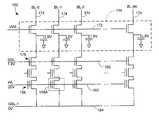
- FIG. 5shows an exemplary schematic representation of portions of the block 150 of FIG. 4A .
- the Flash memory portion 152 of FIG. 4Ais represented by a relatively large dotted line enclosure in FIG. 5 , and is made up of Flash non-volatile memory cells 158 .
- the Flash cellsare arranged into columns 160 and rows 162 , with the Flash cells 158 connected in a NAND configuration along each column.
- the Flash cells 158are further connected along each row 162 via a respective word line 164 , such as the exemplary word line WL-N for row N.
- the DRAM memory portion 154 of FIG. 4Ais represented by a relatively small dotted line enclosure in FIG. 5 , and is shown to be made up of DRAM volatile memory cells 166 each comprising a transistor 168 and a capacitor 170 .
- the transistors 168are connected to a volatile memory cell word line VWL 172 .
- the DRAM cells 166are respectively connected to the Flash cells 158 in each column 160 along respective bit lines 174 .
- the bit lines 174are respectively identified as BL-0 to BL-4K.
- Upper and lower control transistors (MOSFETs) 176 , 178bound each column 160 as shown.
- the gates of the upper transistors 176are connected to a high level source line (SSL) 180
- the gates of the lower transistors 178are connected to a first low level global source line (GSL-0) 182 .
- the drains of the lower transistors 178are connected to a second low level global source line (GSL-1) 184 .
- Read operationscan be carried out on a row-by-row basis, so that the programmed states of the non-volatile memory cells 158 along a given row 162 are retrieved in a page mode operation.
- the contents of row Nare read by applying a gate control voltage to the word line WL-N with a selected magnitude that will differentiate between the different possible programmed states of the Flash cells 158 along the row.
- the cells along row Nwill either transition to a conductive state or remain in a non-conductive state responsive to the applied voltage on WL-N.
- the remaining word lines 164receive a second, higher voltage that will ensure that all of the remaining Flash cells 158 in the block 152 will be placed in a conductive state.
- Suitable voltagesare provided to the SSL and GSL-0 lines 180 , 182 to place the upper and lower transistors 176 , 178 in a conductive state.
- the SSL linemay be provided with a VCC voltage (e.g., +3V) and the GSL-0 line may be provided with a VSS voltage (e.g., ground).
- the GSL-1 linemay also be set to VSS.
- the non-selected word linesmay be provided with a pass voltage of about +5V.
- a voltage sourceapplies the VCC voltage to each of the bit lines BL-0 through BL-4K.
- the capacitor 170 in the DRAM cell 166will store charge to provide a capacitive voltage. It will be appreciated that the storage of charge in this manner constitutes a programming operation on the DRAM cell 166 , and the storage of charge on all of the capacitors 170 can be characterized as the writing of a multi-bit value (e.g., 11111 . . . ) to the row of DRAM cells.
- the time required to store charge on each capacitormay be on the order of the time required to carry out a normal DRAM write operation.
- all of the bit lines 174can be supplied with current simultaneously so that all of the DRAM capacitors 170 store associated amounts of charge simultaneously.
- the voltage sourcecan sequentially apply the requisite charge to each bit line 174 and capacitor 170 in turn.
- the charge stored by a selected volatile memory cell 166is subsequently discharged through the non-volatile memory cells 158 in the associated column.
- This discharged chargeforms a read current that passes through the column, and the sensed voltage across the column generated by this read current can be used to determine the programmed state of the non-volatile cell 158 along the selected row.
- the time required to sense the programmed state of the selected non-volatile cell 158 in a given columnmay be longer than the time required to charge the capacitor 170 in the volatile memory cell 166 associated with the column.
- the sensing operationwill be initiated while charge is being stored by the capacitor 170 and will continue after the voltage source has been decoupled from the transistor, since the discharge of the stored charge will maintain current passing through the column for the sense operation.
- the arraycan be configured such that the capacitor is initially charged and the sense operation does not commence until after the charging operation is completed.
- the voltage sourcecan be decoupled from the bit lines in a number of ways, such as individually by upstream switching circuitry or globally by deasserting the VWL word line 172 .
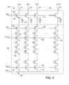
- FIG. 6provides an elevational representation of the block 150 of FIG. 5 in accordance with an exemplary construction.
- a number of localized n+ doped regions 186are formed in a substrate 188 . Adjacent pairs of the doped regions 186 form respective drain and source regions for the respective transistors 158 , 168 , 176 and 178 .
- the capacitor 170 in each columncan be formed from respective cell plates 190 , 192 which extend over the column along the length of the column as shown to take a 128 F 2 (32 ⁇ 4 F 2 ) size, although other sizes and shapes can be used, including a U shaped set of plates.
- each Flash cell 158can be configured with a 2.5 F 2 sized control gate, 70 angstrom tunneling oxide, and 0.5 ratio, and provided with a capacitance of about 15.8 attofarads, aF (15.8 ⁇ 10 ⁇ 18 F). This provides the 32 Flash cells along each column with a combined capacitance of about 0.505 femtofarads, fF (0.505 ⁇ 10 ⁇ 12 F). The total capacitance along a selected bit line will depend on a number of factors including construction, separation and length.
- An exemplary total bit line capacitance value for the block 150may be on the order of about 136 fF.
- using a capacitance for the capacitor 170 that is about one-tenth of this bit line capacitance, i.e. about 13.6 fF for the capacitor 170may provide a 10 to 1 data I/O performance ratio compared to conventional DRAM.
- a value of about 13.6 fF for the capacitor 170is relatively small and is readily achievable using a configuration such as in FIG. 6 .
- a read operation on a conventional Flash blockcan require the application of the pass voltage to the non-selected word lines of each block in turn for a duration of time on the order of about 25 microseconds, ⁇ s (25 ⁇ 10 ⁇ 6 s) in order to output 4K (4096 cells) of data.
- FIG. 7shows a timing diagram 200 to illustrate a timing sequence for read operations upon the exemplary memory array 155 of FIG. 4B . It will be appreciated that the timing diagram 200 is merely representational and is not necessarily drawn to scale.
- An activation pulseis initially represented at 202 , and this represents the concurrent assertion of the non-selected word lines (pass word lines) for all 512 blocks 150 in the array 155 .
- the duration of the pulse 202is represented by the interval 204 and may be on the order of about 200 nanoseconds, ns (200 ⁇ 10 ⁇ 9 s). It is contemplated that the capacitance of the control gates will be sufficient to maintain the non-selected Flash cells in a conductive state throughout the duration of the read operation
- Each of the DRAM VWL word lines(VWL- 0 to VWL- 511 ) are next successively asserted in turn, as shown by pulses 206 .
- These pulsesresult in the charging of the respective capacitors 170 along the respective DRAM rows (portions 154 ) in each block, and the discharge of the charge stored on the capacitors to the bit lines and through the associated columns.
- the pulses 206 in FIG. 7represent the entire interval of time that each bit line is charged, both initially by the bit line voltage source and subsequently by charge transfer from the DRAM capacitor.
- a second curve 208 in FIG. 7generally represents the associated bit line voltage profile for the respective bit lines during the read operation.
- the bit linesmay be precharged to a value of 1 ⁇ 2 VCC (e.g., about 1V), represented by baseline 210 .
- the pass word line activation of pulse 202results in a decay of the bit line voltage at portion 212 , followed by an associated rise portions 214 coincident with assertion of the respective VWL word lines 206 .
- the sensing of data for each block 150will be completed within the charge/discharge interval as indicated by boundary 216 , and the read operation on all 512 blocks will be completed at boundary 218 .
- each charge/discharge interval 206may be on the order of about 30 nanoseconds, ns (30 ⁇ 10 ⁇ 9 s) in duration, with about 10 ns of precharge, 10 ns of hold time, and about 10 ns of charge transfer time after the DRAM word line VWL has been deasserted. These are merely exemplary and other values and ratios can be utilized.
- the volatile memory cellscan further be used to facilitate write (programming) operations upon the non-volatile memory cells (e.g., Flash cells 158 ).
- a programmed statecan be written to a selected Flash memory cell 158 A with the application of a suitable write voltage to the associated word line 162 , such as 20V, and the assertion of the SSL and GSL lines 180 , 184 with 1.8V and 0V.
- the bit line for the selected cell 158 A(in this case, BL-1) is set to 0V and the remaining bit lines are set to 1.8V.
- the desired programmed statewill be provided to the selected Flash cell 158 A while the non-selected cells 158 will fail to receive enough voltage to alter their existing states.
- the various voltages and magnitudesare not limiting and can be a variety of values depending on the requirements of a given application.
- a column of the Flash memory cells 158can be erased in a conventional manner.
- FIG. 9provides a flow chart for a DATA READ routine 220 to summarize various aspects of the foregoing discussion.
- a memory arrayis provided at step 222 with both non-volatile memory cells and volatile memory cells, such as the exemplary Flash cells 158 and DRAM cells 166 discussed above, although this is not limiting.
- Chargeis stored in a selected volatile memory cell at step 224 , and this stored charge is discharged from the volatile memory cell to a selected non-volatile memory cell at step 226 . Such discharge can be used to sense the programmed state of the non-volatile memory cell.
- the various embodiments illustrated hereinprovide advantageous reading of data from a memory array in an efficient manner.
- the use of both volatile and non-volatile memory cells to store and output dataprovides increased data throughput and long term storage.
- the presence of a capacitor or other charge storage deviceallows data to be outputted without the presence of an external voltage and a more rapid successive access to individual blocks of memory cells.
- the various embodiments discussed hereinhave numerous potential applications and are not limited to a certain field of electronic media or type of data storage devices.
- rows and columnswill be read broadly as relational identifiers in an ordered array of elements along different axes without constituting a specific physical layout.
- rowmay constitute a physical column
- columnmay constitute a physical row.
Landscapes
- Engineering & Computer Science (AREA)
- Computer Hardware Design (AREA)
- Read Only Memory (AREA)
- Semiconductor Memories (AREA)
- Dram (AREA)
Abstract
Description
Claims (20)
Priority Applications (3)
| Application Number | Priority Date | Filing Date | Title |
|---|---|---|---|
| US12/474,463US8050092B2 (en) | 2009-05-29 | 2009-05-29 | NAND flash memory with integrated bit line capacitance |
| PCT/US2010/025193WO2010138219A1 (en) | 2009-05-29 | 2010-02-24 | Nand flash memory with integrated bit line capacitance |
| CN201080001812.8ACN102057440B (en) | 2009-05-29 | 2010-02-24 | There is the nand flash memory of integrated bit line capacitance |
Applications Claiming Priority (1)
| Application Number | Priority Date | Filing Date | Title |
|---|---|---|---|
| US12/474,463US8050092B2 (en) | 2009-05-29 | 2009-05-29 | NAND flash memory with integrated bit line capacitance |
Publications (2)
| Publication Number | Publication Date |
|---|---|
| US20100302849A1 US20100302849A1 (en) | 2010-12-02 |
| US8050092B2true US8050092B2 (en) | 2011-11-01 |
Family
ID=42198480
Family Applications (1)
| Application Number | Title | Priority Date | Filing Date |
|---|---|---|---|
| US12/474,463Expired - Fee RelatedUS8050092B2 (en) | 2009-05-29 | 2009-05-29 | NAND flash memory with integrated bit line capacitance |
Country Status (3)
| Country | Link |
|---|---|
| US (1) | US8050092B2 (en) |
| CN (1) | CN102057440B (en) |
| WO (1) | WO2010138219A1 (en) |
Cited By (3)
| Publication number | Priority date | Publication date | Assignee | Title |
|---|---|---|---|---|
| US9390793B1 (en) | 2015-03-20 | 2016-07-12 | Sandisk Technologies Llc | Leakage current compensation with reference bit line sensing in non-volatile memory |
| US9665479B2 (en) | 2014-02-11 | 2017-05-30 | Seagate Technology Llc | Managing response time |
| US9704572B2 (en) | 2015-03-20 | 2017-07-11 | Sandisk Technologies Llc | Sense amplifier with integrating capacitor and methods of operation |
Families Citing this family (8)
| Publication number | Priority date | Publication date | Assignee | Title |
|---|---|---|---|---|
| US20130256777A1 (en) | 2012-03-30 | 2013-10-03 | Seagate Technology Llc | Three dimensional floating gate nand memory |
| US9761310B2 (en) | 2014-09-06 | 2017-09-12 | NEO Semiconductor, Inc. | Method and apparatus for storing information using a memory able to perform both NVM and DRAM functions |
| TWI622055B (en)* | 2014-09-24 | 2018-04-21 | Neo半導體股份有限公司 | Method and apparatus for storing information using a memory able to perform both nvm and dram functions |
| JP6717024B2 (en)* | 2016-04-18 | 2020-07-01 | 富士通株式会社 | MEMORY AND MEMORY CONTROL METHOD |
| US10282108B2 (en)* | 2016-08-31 | 2019-05-07 | Micron Technology, Inc. | Hybrid memory device using different types of capacitors |
| US11361813B2 (en) | 2016-09-16 | 2022-06-14 | Aspiring Sky Co. Limited | Nonvolatile memory structures with DRAM |
| US10354716B2 (en)* | 2016-09-16 | 2019-07-16 | Aspiring Sky Co. Limited | SRAM based memory structures and methods thereof |
| US20200378513A1 (en)* | 2019-05-31 | 2020-12-03 | Robert Kowalski | Heated Faucet Cover |
Citations (17)
| Publication number | Priority date | Publication date | Assignee | Title |
|---|---|---|---|---|
| US5455786A (en)* | 1993-06-23 | 1995-10-03 | Hitachi, Ltd. | Ferroelectric memory |
| US5623442A (en)* | 1993-07-13 | 1997-04-22 | Nkk Corporation | Memory cells and memory devices with a storage capacitor of parasitic capacitance and information storing method using the same |
| US5768208A (en)* | 1996-06-18 | 1998-06-16 | Microchip Technology Incorporated | Fail safe non-volatile memory programming system and method therefor |
| US6198652B1 (en)* | 1998-04-13 | 2001-03-06 | Kabushiki Kaisha Toshiba | Non-volatile semiconductor integrated memory device |
| US6201733B1 (en)* | 1998-11-11 | 2001-03-13 | Hitachi, Ltd. | Semiconductor integrated circuit device, memory module and storage device |
| US6528839B2 (en)* | 1999-02-01 | 2003-03-04 | Shoji Shukuri | Semiconductor integrated circuit and nonvolatile memory element |
| US6992928B2 (en)* | 2002-04-11 | 2006-01-31 | Elpida Memory, Inc. | Semiconductor memory device with an improved memory cell structure and method of operating the same |
| US7180787B2 (en)* | 2004-03-29 | 2007-02-20 | Kabushiki Kaisha Toshiba | Semiconductor memory device |
| US7319613B2 (en) | 2004-02-10 | 2008-01-15 | Micron Technology, Inc. | NROM flash memory cell with integrated DRAM |
| US7333363B2 (en)* | 2005-04-25 | 2008-02-19 | Elpida Memory, Inc. | Semiconductor storage apparatus |
| US7397686B2 (en) | 2005-06-02 | 2008-07-08 | Kabushiki Kaisha Toshiba | Memory system combining flash EEPROM and FeRAM |
| US7414888B2 (en)* | 2005-09-22 | 2008-08-19 | Macronix International Co., Ltd. | Program method and circuit of non-volatile memory |
| US7417893B2 (en) | 2004-08-27 | 2008-08-26 | Micron Technology, Inc. | Integrated DRAM-NVRAM multi-level memory |
| US7697333B2 (en)* | 2006-08-16 | 2010-04-13 | Kabushiki Kaisha Toshiba | NAND flash memory |
| US7782683B2 (en)* | 2004-01-30 | 2010-08-24 | Samsung Electronics Co., Ltd. | Multi-port memory device for buffering between hosts and non-volatile memory devices |
| US7859899B1 (en)* | 2008-03-28 | 2010-12-28 | Cypress Semiconductor Corporation | Non-volatile memory and method of operating the same |
| US7872919B2 (en)* | 2008-06-30 | 2011-01-18 | Kabushiki Kaisha Toshiba | Semiconductor memory device |
Family Cites Families (5)
| Publication number | Priority date | Publication date | Assignee | Title |
|---|---|---|---|---|
| US7177197B2 (en)* | 2001-09-17 | 2007-02-13 | Sandisk Corporation | Latched programming of memory and method |
| ITMI20022464A1 (en)* | 2002-11-20 | 2004-05-21 | Simicroelectronics S R L | SEMICONDUCTOR MEMORY WITH BUILT-IN DRAM |
| JP4287235B2 (en)* | 2003-10-09 | 2009-07-01 | 株式会社東芝 | Nonvolatile semiconductor memory device |
| US20080158986A1 (en)* | 2006-12-29 | 2008-07-03 | Daniel Elmhurst | Flash memory and associated methods |
| KR101100359B1 (en)* | 2006-12-29 | 2011-12-30 | 샌디스크 코포레이션 | How to Read a Nonvolatile Memory Cell Considering the Storage State of Adjacent Memory Cells |
- 2009
- 2009-05-29USUS12/474,463patent/US8050092B2/ennot_activeExpired - Fee Related
- 2010
- 2010-02-24WOPCT/US2010/025193patent/WO2010138219A1/enactiveApplication Filing
- 2010-02-24CNCN201080001812.8Apatent/CN102057440B/ennot_activeExpired - Fee Related
Patent Citations (18)
| Publication number | Priority date | Publication date | Assignee | Title |
|---|---|---|---|---|
| US5455786A (en)* | 1993-06-23 | 1995-10-03 | Hitachi, Ltd. | Ferroelectric memory |
| US5623442A (en)* | 1993-07-13 | 1997-04-22 | Nkk Corporation | Memory cells and memory devices with a storage capacitor of parasitic capacitance and information storing method using the same |
| US5768208A (en)* | 1996-06-18 | 1998-06-16 | Microchip Technology Incorporated | Fail safe non-volatile memory programming system and method therefor |
| US6198652B1 (en)* | 1998-04-13 | 2001-03-06 | Kabushiki Kaisha Toshiba | Non-volatile semiconductor integrated memory device |
| US6201733B1 (en)* | 1998-11-11 | 2001-03-13 | Hitachi, Ltd. | Semiconductor integrated circuit device, memory module and storage device |
| US6528839B2 (en)* | 1999-02-01 | 2003-03-04 | Shoji Shukuri | Semiconductor integrated circuit and nonvolatile memory element |
| US6992928B2 (en)* | 2002-04-11 | 2006-01-31 | Elpida Memory, Inc. | Semiconductor memory device with an improved memory cell structure and method of operating the same |
| US7782683B2 (en)* | 2004-01-30 | 2010-08-24 | Samsung Electronics Co., Ltd. | Multi-port memory device for buffering between hosts and non-volatile memory devices |
| US7319613B2 (en) | 2004-02-10 | 2008-01-15 | Micron Technology, Inc. | NROM flash memory cell with integrated DRAM |
| US7180787B2 (en)* | 2004-03-29 | 2007-02-20 | Kabushiki Kaisha Toshiba | Semiconductor memory device |
| US7417893B2 (en) | 2004-08-27 | 2008-08-26 | Micron Technology, Inc. | Integrated DRAM-NVRAM multi-level memory |
| US7333363B2 (en)* | 2005-04-25 | 2008-02-19 | Elpida Memory, Inc. | Semiconductor storage apparatus |
| US7508707B2 (en)* | 2005-04-25 | 2009-03-24 | Elpida Memory, Inc. | Semiconductor storage apparatus |
| US7397686B2 (en) | 2005-06-02 | 2008-07-08 | Kabushiki Kaisha Toshiba | Memory system combining flash EEPROM and FeRAM |
| US7414888B2 (en)* | 2005-09-22 | 2008-08-19 | Macronix International Co., Ltd. | Program method and circuit of non-volatile memory |
| US7697333B2 (en)* | 2006-08-16 | 2010-04-13 | Kabushiki Kaisha Toshiba | NAND flash memory |
| US7859899B1 (en)* | 2008-03-28 | 2010-12-28 | Cypress Semiconductor Corporation | Non-volatile memory and method of operating the same |
| US7872919B2 (en)* | 2008-06-30 | 2011-01-18 | Kabushiki Kaisha Toshiba | Semiconductor memory device |
Cited By (3)
| Publication number | Priority date | Publication date | Assignee | Title |
|---|---|---|---|---|
| US9665479B2 (en) | 2014-02-11 | 2017-05-30 | Seagate Technology Llc | Managing response time |
| US9390793B1 (en) | 2015-03-20 | 2016-07-12 | Sandisk Technologies Llc | Leakage current compensation with reference bit line sensing in non-volatile memory |
| US9704572B2 (en) | 2015-03-20 | 2017-07-11 | Sandisk Technologies Llc | Sense amplifier with integrating capacitor and methods of operation |
Also Published As
| Publication number | Publication date |
|---|---|
| WO2010138219A1 (en) | 2010-12-02 |
| CN102057440B (en) | 2015-11-25 |
| US20100302849A1 (en) | 2010-12-02 |
| CN102057440A (en) | 2011-05-11 |
Similar Documents
| Publication | Publication Date | Title |
|---|---|---|
| US8050092B2 (en) | NAND flash memory with integrated bit line capacitance | |
| US7800953B2 (en) | Method and system for selectively limiting peak power consumption during programming or erase of non-volatile memory devices | |
| US9953717B2 (en) | NAND structure with tier select gate transistors | |
| US7362616B2 (en) | NAND flash memory with erase verify based on shorter evaluation time | |
| JP5642649B2 (en) | Semiconductor memory device and semiconductor device | |
| US8472254B2 (en) | Memory arrays and memory devices | |
| JP4038823B2 (en) | Semiconductor nonvolatile memory device and computer system using the same | |
| US7577031B2 (en) | Non-volatile memory with compensation for variations along a word line | |
| US11404122B2 (en) | Sub-block size reduction for 3D non-volatile memory | |
| KR920017121A (en) | Electrically Erasable and Programmable Read-Only Storage Devices with Verification Control Circuits | |
| JP2010522951A (en) | Nonvolatile memory and method for compensating voltage drop along a word line | |
| US20080239813A1 (en) | Method of Compensating Variations along a Word Line in a Non-Volatile Memory | |
| JP2008535140A (en) | Nonvolatile memory and method using compensation for source line bias error | |
| US9361976B2 (en) | Sense amplifier including a single-transistor amplifier and level shifter and methods therefor | |
| CN101123120A (en) | One-time programming memory using resistive storage medium and operating method thereof | |
| KR100843210B1 (en) | Resistive Memory Device and Data Writing Method | |
| KR20180001710A (en) | Nonvolatile memory device and erasing method of nonvolatile memory device | |
| US10685717B2 (en) | Erasing memory cells | |
| CN103383862B (en) | Integrated circuit device and method of operating the same | |
| JP4790335B2 (en) | Nonvolatile semiconductor memory device | |
| US7830708B1 (en) | Compensating for variations in memory cell programmed state distributions | |
| KR102861570B1 (en) | Memory device having page buffer | |
| US12347510B2 (en) | Bonding defect detection for die-to-die bonding in memory devices | |
| EP1752989B1 (en) | NAND flash memory with erase verify based on shorter delay before sensing | |
| JP2006286190A (en) | Semiconductor nonvolatile memory device and computer system using the same |
Legal Events
| Date | Code | Title | Description |
|---|---|---|---|
| AS | Assignment | Owner name:SEAGATE TECHNOLOGY LLC, CALIFORNIA Free format text:ASSIGNMENT OF ASSIGNORS INTEREST;ASSIGNORS:JUNG, CHULMIN;LIU, HARRY HONGYUE;LEE, BRIAN;AND OTHERS;REEL/FRAME:022752/0104 Effective date:20090528 | |
| AS | Assignment | Owner name:THE BANK OF NOVA SCOTIA, AS ADMINISTRATIVE AGENT, CANADA Free format text:SECURITY AGREEMENT;ASSIGNOR:SEAGATE TECHNOLOGY LLC;REEL/FRAME:026010/0350 Effective date:20110118 Owner name:THE BANK OF NOVA SCOTIA, AS ADMINISTRATIVE AGENT, Free format text:SECURITY AGREEMENT;ASSIGNOR:SEAGATE TECHNOLOGY LLC;REEL/FRAME:026010/0350 Effective date:20110118 | |
| ZAAA | Notice of allowance and fees due | Free format text:ORIGINAL CODE: NOA | |
| ZAAB | Notice of allowance mailed | Free format text:ORIGINAL CODE: MN/=. | |
| STCF | Information on status: patent grant | Free format text:PATENTED CASE | |
| AS | Assignment | Owner name:THE BANK OF NOVA SCOTIA, AS ADMINISTRATIVE AGENT, CANADA Free format text:SECURITY AGREEMENT;ASSIGNORS:SEAGATE TECHNOLOGY LLC;EVAULT, INC. (F/K/A I365 INC.);SEAGATE TECHNOLOGY US HOLDINGS, INC.;REEL/FRAME:029127/0527 Effective date:20120718 Owner name:WELLS FARGO BANK, NATIONAL ASSOCIATION, AS COLLATERAL AGENT, CALIFORNIA Free format text:SECOND LIEN PATENT SECURITY AGREEMENT;ASSIGNORS:SEAGATE TECHNOLOGY LLC;EVAULT, INC. (F/K/A I365 INC.);SEAGATE TECHNOLOGY US HOLDINGS, INC.;REEL/FRAME:029253/0585 Effective date:20120718 Owner name:THE BANK OF NOVA SCOTIA, AS ADMINISTRATIVE AGENT, Free format text:SECURITY AGREEMENT;ASSIGNORS:SEAGATE TECHNOLOGY LLC;EVAULT, INC. (F/K/A I365 INC.);SEAGATE TECHNOLOGY US HOLDINGS, INC.;REEL/FRAME:029127/0527 Effective date:20120718 Owner name:WELLS FARGO BANK, NATIONAL ASSOCIATION, AS COLLATE Free format text:SECOND LIEN PATENT SECURITY AGREEMENT;ASSIGNORS:SEAGATE TECHNOLOGY LLC;EVAULT, INC. (F/K/A I365 INC.);SEAGATE TECHNOLOGY US HOLDINGS, INC.;REEL/FRAME:029253/0585 Effective date:20120718 | |
| FEPP | Fee payment procedure | Free format text:PAYOR NUMBER ASSIGNED (ORIGINAL EVENT CODE: ASPN); ENTITY STATUS OF PATENT OWNER: LARGE ENTITY | |
| FPAY | Fee payment | Year of fee payment:4 | |
| FEPP | Fee payment procedure | Free format text:7.5 YR SURCHARGE - LATE PMT W/IN 6 MO, LARGE ENTITY (ORIGINAL EVENT CODE: M1555); ENTITY STATUS OF PATENT OWNER: LARGE ENTITY | |
| MAFP | Maintenance fee payment | Free format text:PAYMENT OF MAINTENANCE FEE, 8TH YEAR, LARGE ENTITY (ORIGINAL EVENT CODE: M1552); ENTITY STATUS OF PATENT OWNER: LARGE ENTITY Year of fee payment:8 | |
| FEPP | Fee payment procedure | Free format text:MAINTENANCE FEE REMINDER MAILED (ORIGINAL EVENT CODE: REM.); ENTITY STATUS OF PATENT OWNER: LARGE ENTITY | |
| LAPS | Lapse for failure to pay maintenance fees | Free format text:PATENT EXPIRED FOR FAILURE TO PAY MAINTENANCE FEES (ORIGINAL EVENT CODE: EXP.); ENTITY STATUS OF PATENT OWNER: LARGE ENTITY | |
| STCH | Information on status: patent discontinuation | Free format text:PATENT EXPIRED DUE TO NONPAYMENT OF MAINTENANCE FEES UNDER 37 CFR 1.362 | |
| FP | Lapsed due to failure to pay maintenance fee | Effective date:20231101 | |
| AS | Assignment | Owner name:SEAGATE TECHNOLOGY US HOLDINGS, INC., CALIFORNIA Free format text:RELEASE BY SECURED PARTY;ASSIGNOR:WELLS FARGO BANK, NATIONAL ASSOCIATION, AS COLLATERAL AGENT;REEL/FRAME:067471/0955 Effective date:20240516 Owner name:EVAULT, INC. (F/K/A I365 INC.), CALIFORNIA Free format text:RELEASE BY SECURED PARTY;ASSIGNOR:WELLS FARGO BANK, NATIONAL ASSOCIATION, AS COLLATERAL AGENT;REEL/FRAME:067471/0955 Effective date:20240516 Owner name:SEAGATE TECHNOLOGY LLC, CALIFORNIA Free format text:RELEASE BY SECURED PARTY;ASSIGNOR:WELLS FARGO BANK, NATIONAL ASSOCIATION, AS COLLATERAL AGENT;REEL/FRAME:067471/0955 Effective date:20240516 | |
| AS | Assignment | Owner name:EVAULT INC, CALIFORNIA Free format text:RELEASE BY SECURED PARTY;ASSIGNOR:WELLS FARGO BANK, NATIONAL ASSOCIATION, AS COLLATERAL AGENT;REEL/FRAME:068457/0076 Effective date:20240723 Owner name:SEAGATE TECHNOLOGY LLC, CALIFORNIA Free format text:RELEASE BY SECURED PARTY;ASSIGNOR:WELLS FARGO BANK, NATIONAL ASSOCIATION, AS COLLATERAL AGENT;REEL/FRAME:068457/0076 Effective date:20240723 | |
| AS | Assignment | Owner name:SEAGATE TECHNOLOGY LLC, CALIFORNIA Free format text:RELEASE BY SECURED PARTY;ASSIGNOR:THE BANK OF NOVA SCOTIA;REEL/FRAME:070363/0903 Effective date:20241223 Owner name:EVAULT, INC. (F/K/A I365 INC.), CALIFORNIA Free format text:RELEASE BY SECURED PARTY;ASSIGNOR:THE BANK OF NOVA SCOTIA;REEL/FRAME:070363/0903 Effective date:20241223 Owner name:SEAGATE TECHNOLOGY US HOLDINGS, INC., CALIFORNIA Free format text:RELEASE BY SECURED PARTY;ASSIGNOR:THE BANK OF NOVA SCOTIA;REEL/FRAME:070363/0903 Effective date:20241223 | |
| AS | Assignment | Owner name:SEAGATE TECHNOLOGY PUBLIC LIMITED COMPANY, CALIFORNIA Free format text:RELEASE BY SECURED PARTY;ASSIGNOR:THE BANK OF NOVA SCOTIA;REEL/FRAME:072193/0001 Effective date:20250303 Owner name:SEAGATE TECHNOLOGY, CALIFORNIA Free format text:RELEASE BY SECURED PARTY;ASSIGNOR:THE BANK OF NOVA SCOTIA;REEL/FRAME:072193/0001 Effective date:20250303 Owner name:SEAGATE TECHNOLOGY HDD HOLDINGS, CALIFORNIA Free format text:RELEASE BY SECURED PARTY;ASSIGNOR:THE BANK OF NOVA SCOTIA;REEL/FRAME:072193/0001 Effective date:20250303 Owner name:I365 INC., CALIFORNIA Free format text:RELEASE BY SECURED PARTY;ASSIGNOR:THE BANK OF NOVA SCOTIA;REEL/FRAME:072193/0001 Effective date:20250303 Owner name:SEAGATE TECHNOLOGY LLC, CALIFORNIA Free format text:RELEASE BY SECURED PARTY;ASSIGNOR:THE BANK OF NOVA SCOTIA;REEL/FRAME:072193/0001 Effective date:20250303 Owner name:SEAGATE TECHNOLOGY INTERNATIONAL, CAYMAN ISLANDS Free format text:RELEASE BY SECURED PARTY;ASSIGNOR:THE BANK OF NOVA SCOTIA;REEL/FRAME:072193/0001 Effective date:20250303 Owner name:SEAGATE HDD CAYMAN, CAYMAN ISLANDS Free format text:RELEASE BY SECURED PARTY;ASSIGNOR:THE BANK OF NOVA SCOTIA;REEL/FRAME:072193/0001 Effective date:20250303 Owner name:SEAGATE TECHNOLOGY (US) HOLDINGS, INC., CALIFORNIA Free format text:RELEASE BY SECURED PARTY;ASSIGNOR:THE BANK OF NOVA SCOTIA;REEL/FRAME:072193/0001 Effective date:20250303 |