US8049947B2 - Components and methods for use in electro-optic displays - Google Patents
Components and methods for use in electro-optic displaysDownload PDFInfo
- Publication number
- US8049947B2 US8049947B2US12/550,470US55047009AUS8049947B2US 8049947 B2US8049947 B2US 8049947B2US 55047009 AUS55047009 AUS 55047009AUS 8049947 B2US8049947 B2US 8049947B2
- Authority
- US
- United States
- Prior art keywords
- layer
- electro
- backplane
- optic
- areas
- Prior art date
- Legal status (The legal status is an assumption and is not a legal conclusion. Google has not performed a legal analysis and makes no representation as to the accuracy of the status listed.)
- Expired - Fee Related, expires
Links
- 238000000034methodMethods0.000titleclaimsabstractdescription161
- 239000010410layerSubstances0.000claimsabstractdescription239
- 239000012790adhesive layerSubstances0.000claimsabstractdescription149
- 230000008569processEffects0.000claimsabstractdescription132
- 239000007787solidSubstances0.000claimsabstractdescription63
- 239000000758substrateSubstances0.000claimsdescription106
- 239000000382optic materialSubstances0.000claimsdescription94
- 239000000463materialSubstances0.000claimsdescription25
- 239000012530fluidSubstances0.000claimsdescription23
- 239000002245particleSubstances0.000claimsdescription21
- 230000000873masking effectEffects0.000claimsdescription19
- 239000011241protective layerSubstances0.000claimsdescription13
- 239000002775capsuleSubstances0.000claimsdescription11
- 230000005684electric fieldEffects0.000claimsdescription8
- 238000003475laminationMethods0.000abstractdescription43
- 238000000429assemblyMethods0.000description26
- 239000000853adhesiveSubstances0.000description25
- 230000001070adhesive effectEffects0.000description25
- 238000004519manufacturing processMethods0.000description21
- 230000003287optical effectEffects0.000description13
- 238000000576coating methodMethods0.000description11
- 239000011248coating agentSubstances0.000description10
- 230000008901benefitEffects0.000description9
- 238000005520cutting processMethods0.000description9
- 239000007788liquidSubstances0.000description9
- 239000004973liquid crystal related substanceSubstances0.000description8
- 238000010030laminatingMethods0.000description7
- 230000008859changeEffects0.000description6
- -1Poly(ethylene terephthalate)Polymers0.000description5
- 239000011230binding agentSubstances0.000description5
- 238000003698laser cuttingMethods0.000description5
- 238000007639printingMethods0.000description5
- 229920000139polyethylene terephthalatePolymers0.000description4
- 239000005020polyethylene terephthalateSubstances0.000description4
- 238000012545processingMethods0.000description4
- 238000000926separation methodMethods0.000description4
- 238000012360testing methodMethods0.000description4
- 230000000694effectsEffects0.000description3
- 239000007789gasSubstances0.000description3
- AMGQUBHHOARCQH-UHFFFAOYSA-Nindium;oxotinChemical compound[In].[Sn]=OAMGQUBHHOARCQH-UHFFFAOYSA-N0.000description3
- 239000011159matrix materialSubstances0.000description3
- 239000003094microcapsuleSubstances0.000description3
- 239000002985plastic filmSubstances0.000description3
- 229920006255plastic filmPolymers0.000description3
- 230000000717retained effectEffects0.000description3
- 229920002799BoPETPolymers0.000description2
- 229910052782aluminiumInorganic materials0.000description2
- XAGFODPZIPBFFR-UHFFFAOYSA-NaluminiumChemical compound[Al]XAGFODPZIPBFFR-UHFFFAOYSA-N0.000description2
- 230000005540biological transmissionEffects0.000description2
- 230000001427coherent effectEffects0.000description2
- 239000004020conductorSubstances0.000description2
- 230000006870functionEffects0.000description2
- 238000003384imaging methodMethods0.000description2
- 239000003550markerSubstances0.000description2
- 229910052751metalInorganic materials0.000description2
- 239000002184metalSubstances0.000description2
- 230000004044responseEffects0.000description2
- 210000003934vacuoleAnatomy0.000description2
- 239000002699waste materialSubstances0.000description2
- 238000009736wettingMethods0.000description2
- 229920000134Metallised filmPolymers0.000description1
- 239000005041Mylar™Substances0.000description1
- 241001422033ThestylusSpecies0.000description1
- 238000010521absorption reactionMethods0.000description1
- 208000033853acromesomelic dysplasia 4Diseases0.000description1
- 239000002313adhesive filmSubstances0.000description1
- 238000007754air knife coatingMethods0.000description1
- 230000000712assemblyEffects0.000description1
- QVGXLLKOCUKJST-UHFFFAOYSA-Natomic oxygenChemical compound[O]QVGXLLKOCUKJST-UHFFFAOYSA-N0.000description1
- 230000004888barrier functionEffects0.000description1
- 230000015572biosynthetic processEffects0.000description1
- 230000001413cellular effectEffects0.000description1
- 239000012612commercial materialSubstances0.000description1
- 229920001940conductive polymerPolymers0.000description1
- 238000011109contaminationMethods0.000description1
- 238000007766curtain coatingMethods0.000description1
- 230000000593degrading effectEffects0.000description1
- 238000007607die coating methodMethods0.000description1
- 238000003618dip coatingMethods0.000description1
- 239000000428dustSubstances0.000description1
- 238000001652electrophoretic depositionMethods0.000description1
- 238000005516engineering processMethods0.000description1
- 238000007765extrusion coatingMethods0.000description1
- 239000012467final productSubstances0.000description1
- 239000011521glassSubstances0.000description1
- 238000007756gravure coatingMethods0.000description1
- 238000010348incorporationMethods0.000description1
- 238000007641inkjet printingMethods0.000description1
- 238000009685knife-over-roll coatingMethods0.000description1
- 238000011031large-scale manufacturing processMethods0.000description1
- 230000007774longtermEffects0.000description1
- 238000004020luminiscence typeMethods0.000description1
- 238000007567mass-production techniqueMethods0.000description1
- 239000012528membraneSubstances0.000description1
- 230000005499meniscusEffects0.000description1
- 229910044991metal oxideInorganic materials0.000description1
- 150000004706metal oxidesChemical class0.000description1
- 238000012986modificationMethods0.000description1
- 230000004048modificationEffects0.000description1
- 239000001301oxygenSubstances0.000description1
- 229910052760oxygenInorganic materials0.000description1
- 239000000047productSubstances0.000description1
- 238000002310reflectometryMethods0.000description1
- 238000012827research and developmentMethods0.000description1
- 238000007763reverse roll coatingMethods0.000description1
- 230000002441reversible effectEffects0.000description1
- 238000006748scratchingMethods0.000description1
- 230000002393scratching effectEffects0.000description1
- 238000007650screen-printingMethods0.000description1
- 238000004528spin coatingMethods0.000description1
- 238000005507sprayingMethods0.000description1
- 239000007858starting materialSubstances0.000description1
- 238000007651thermal printingMethods0.000description1
- 238000012546transferMethods0.000description1
- 230000000007visual effectEffects0.000description1
- XLYOFNOQVPJJNP-UHFFFAOYSA-NwaterChemical compoundOXLYOFNOQVPJJNP-UHFFFAOYSA-N0.000description1
- 239000002023woodSubstances0.000description1
Images


Classifications
- G—PHYSICS
- G02—OPTICS
- G02F—OPTICAL DEVICES OR ARRANGEMENTS FOR THE CONTROL OF LIGHT BY MODIFICATION OF THE OPTICAL PROPERTIES OF THE MEDIA OF THE ELEMENTS INVOLVED THEREIN; NON-LINEAR OPTICS; FREQUENCY-CHANGING OF LIGHT; OPTICAL LOGIC ELEMENTS; OPTICAL ANALOGUE/DIGITAL CONVERTERS
- G02F1/00—Devices or arrangements for the control of the intensity, colour, phase, polarisation or direction of light arriving from an independent light source, e.g. switching, gating or modulating; Non-linear optics
- G02F1/01—Devices or arrangements for the control of the intensity, colour, phase, polarisation or direction of light arriving from an independent light source, e.g. switching, gating or modulating; Non-linear optics for the control of the intensity, phase, polarisation or colour
- G02F1/165—Devices or arrangements for the control of the intensity, colour, phase, polarisation or direction of light arriving from an independent light source, e.g. switching, gating or modulating; Non-linear optics for the control of the intensity, phase, polarisation or colour based on translational movement of particles in a fluid under the influence of an applied field
- G02F1/166—Devices or arrangements for the control of the intensity, colour, phase, polarisation or direction of light arriving from an independent light source, e.g. switching, gating or modulating; Non-linear optics for the control of the intensity, phase, polarisation or colour based on translational movement of particles in a fluid under the influence of an applied field characterised by the electro-optical or magneto-optical effect
- G02F1/167—Devices or arrangements for the control of the intensity, colour, phase, polarisation or direction of light arriving from an independent light source, e.g. switching, gating or modulating; Non-linear optics for the control of the intensity, phase, polarisation or colour based on translational movement of particles in a fluid under the influence of an applied field characterised by the electro-optical or magneto-optical effect by electrophoresis
- B—PERFORMING OPERATIONS; TRANSPORTING
- B32—LAYERED PRODUCTS
- B32B—LAYERED PRODUCTS, i.e. PRODUCTS BUILT-UP OF STRATA OF FLAT OR NON-FLAT, e.g. CELLULAR OR HONEYCOMB, FORM
- B32B38/00—Ancillary operations in connection with laminating processes
- B32B38/10—Removing layers, or parts of layers, mechanically or chemically
- B—PERFORMING OPERATIONS; TRANSPORTING
- B32—LAYERED PRODUCTS
- B32B—LAYERED PRODUCTS, i.e. PRODUCTS BUILT-UP OF STRATA OF FLAT OR NON-FLAT, e.g. CELLULAR OR HONEYCOMB, FORM
- B32B2457/00—Electrical equipment
- B32B2457/20—Displays, e.g. liquid crystal displays, plasma displays
- B—PERFORMING OPERATIONS; TRANSPORTING
- B32—LAYERED PRODUCTS
- B32B—LAYERED PRODUCTS, i.e. PRODUCTS BUILT-UP OF STRATA OF FLAT OR NON-FLAT, e.g. CELLULAR OR HONEYCOMB, FORM
- B32B37/00—Methods or apparatus for laminating, e.g. by curing or by ultrasonic bonding
- B32B37/12—Methods or apparatus for laminating, e.g. by curing or by ultrasonic bonding characterised by using adhesives
- G—PHYSICS
- G02—OPTICS
- G02F—OPTICAL DEVICES OR ARRANGEMENTS FOR THE CONTROL OF LIGHT BY MODIFICATION OF THE OPTICAL PROPERTIES OF THE MEDIA OF THE ELEMENTS INVOLVED THEREIN; NON-LINEAR OPTICS; FREQUENCY-CHANGING OF LIGHT; OPTICAL LOGIC ELEMENTS; OPTICAL ANALOGUE/DIGITAL CONVERTERS
- G02F1/00—Devices or arrangements for the control of the intensity, colour, phase, polarisation or direction of light arriving from an independent light source, e.g. switching, gating or modulating; Non-linear optics
- G02F1/01—Devices or arrangements for the control of the intensity, colour, phase, polarisation or direction of light arriving from an independent light source, e.g. switching, gating or modulating; Non-linear optics for the control of the intensity, phase, polarisation or colour
- G02F1/13—Devices or arrangements for the control of the intensity, colour, phase, polarisation or direction of light arriving from an independent light source, e.g. switching, gating or modulating; Non-linear optics for the control of the intensity, phase, polarisation or colour based on liquid crystals, e.g. single liquid crystal display cells
- G02F1/133—Constructional arrangements; Operation of liquid crystal cells; Circuit arrangements
- G02F1/1333—Constructional arrangements; Manufacturing methods
- G02F1/133377—Cells with plural compartments or having plurality of liquid crystal microcells partitioned by walls, e.g. one microcell per pixel
- G—PHYSICS
- G02—OPTICS
- G02F—OPTICAL DEVICES OR ARRANGEMENTS FOR THE CONTROL OF LIGHT BY MODIFICATION OF THE OPTICAL PROPERTIES OF THE MEDIA OF THE ELEMENTS INVOLVED THEREIN; NON-LINEAR OPTICS; FREQUENCY-CHANGING OF LIGHT; OPTICAL LOGIC ELEMENTS; OPTICAL ANALOGUE/DIGITAL CONVERTERS
- G02F1/00—Devices or arrangements for the control of the intensity, colour, phase, polarisation or direction of light arriving from an independent light source, e.g. switching, gating or modulating; Non-linear optics
- G02F1/01—Devices or arrangements for the control of the intensity, colour, phase, polarisation or direction of light arriving from an independent light source, e.g. switching, gating or modulating; Non-linear optics for the control of the intensity, phase, polarisation or colour
- G02F1/165—Devices or arrangements for the control of the intensity, colour, phase, polarisation or direction of light arriving from an independent light source, e.g. switching, gating or modulating; Non-linear optics for the control of the intensity, phase, polarisation or colour based on translational movement of particles in a fluid under the influence of an applied field
- G02F1/1675—Constructional details
- G02F1/1679—Gaskets; Spacers; Sealing of cells; Filling or closing of cells
- G02F1/1681—Gaskets; Spacers; Sealing of cells; Filling or closing of cells having two or more microcells partitioned by walls, e.g. of microcup type
- Y—GENERAL TAGGING OF NEW TECHNOLOGICAL DEVELOPMENTS; GENERAL TAGGING OF CROSS-SECTIONAL TECHNOLOGIES SPANNING OVER SEVERAL SECTIONS OF THE IPC; TECHNICAL SUBJECTS COVERED BY FORMER USPC CROSS-REFERENCE ART COLLECTIONS [XRACs] AND DIGESTS
- Y10—TECHNICAL SUBJECTS COVERED BY FORMER USPC
- Y10T—TECHNICAL SUBJECTS COVERED BY FORMER US CLASSIFICATION
- Y10T156/00—Adhesive bonding and miscellaneous chemical manufacture
- Y10T156/10—Methods of surface bonding and/or assembly therefor
- Y10T156/1052—Methods of surface bonding and/or assembly therefor with cutting, punching, tearing or severing
- Y—GENERAL TAGGING OF NEW TECHNOLOGICAL DEVELOPMENTS; GENERAL TAGGING OF CROSS-SECTIONAL TECHNOLOGIES SPANNING OVER SEVERAL SECTIONS OF THE IPC; TECHNICAL SUBJECTS COVERED BY FORMER USPC CROSS-REFERENCE ART COLLECTIONS [XRACs] AND DIGESTS
- Y10—TECHNICAL SUBJECTS COVERED BY FORMER USPC
- Y10T—TECHNICAL SUBJECTS COVERED BY FORMER US CLASSIFICATION
- Y10T156/00—Adhesive bonding and miscellaneous chemical manufacture
- Y10T156/10—Methods of surface bonding and/or assembly therefor
- Y10T156/1089—Methods of surface bonding and/or assembly therefor of discrete laminae to single face of additional lamina
- Y10T156/1092—All laminae planar and face to face
- Y10T156/1093—All laminae planar and face to face with covering of discrete laminae with additional lamina
Definitions
- 11/850,831is also a continuation-in-part of application Ser. No. 11/747,546, filed May 11, 2007 (now U.S. Pat. No. 7,443,571, issued Oct. 28, 2008), which is a continuation of application Ser. No. 10/907,065, filed Mar. 18, 2005 (now U.S. Pat. No. 7,236,292), which is a divisional of application Ser. No. 10/249,957, filed May 22, 2003 (now U.S. Pat. No. 6,982,178), which claims benefit of Application Ser. No. 60/319,300, filed Jun. 10, 2002, and Application Ser. No. 60/320,186, filed May 12, 2003.
- This applicationis also related to:
- This inventionrelates to components and methods for use in electro-optic displays. More specifically, this invention relates to methods for the manufacture of electro-optic displays, and to certain sub-assemblies produced during such methods. This invention primarily relates to such methods and sub-assemblies for forming electro-optic displays containing an electro-optic medium which is a solid (such displays may hereinafter for convenience be referred to as “solid electro-optic displays”), in the sense that the electro-optic medium has solid external surfaces, although the medium may, and often does, have internal liquid- or gas-filled spaces, and to methods for assembling displays using such an electro-optic medium.
- solid electro-optic displaysincludes encapsulated electrophoretic displays, encapsulated liquid crystal displays, and other types of displays discussed below.
- optical propertyis typically color perceptible to the human eye, it may be another optical property, such as optical transmission, reflectance, luminescence or, in the case of displays intended for machine reading, pseudo-color in the sense of a change in reflectance of electromagnetic wavelengths outside the visible range.
- bistable and “bistability”are used herein in their conventional meaning in the art to refer to displays comprising display elements having first and second display states differing in at least one optical property, and such that after any given element has been driven, by means of an addressing pulse of finite duration, to assume either its first or second display state, after the addressing pulse has terminated, that state will persist for at least several times, for example at least four times, the minimum duration of the addressing pulse required to change the state of the display element.
- addressing pulseof finite duration
- some particle-based electrophoretic displays capable of gray scaleare stable not only in their extreme black and white states but also in their intermediate gray states, and the same is true of some other types of electro-optic displays.
- This type of displayis properly called “multi-stable” rather than bistable, although for convenience the term “bistable” may be used herein to cover both bistable and multi-stable displays.
- electro-optic displaysare known.
- One type of electro-optic displayis a rotating bichromal member type as described, for example, in U.S. Pat. Nos. 5,808,783; 5,777,782; 5,760,761; 6,054,071 6,055,091; 6,097,531; 6,128,124; 6,137,467; and 6,147,791 (although this type of display is often referred to as a “rotating bichromal ball” display, the term “rotating bichromal member” is preferred as more accurate since in some of the patents mentioned above the rotating members are not spherical).
- Such a displayuses a large number of small bodies (typically spherical or cylindrical) which have two or more sections with differing optical characteristics, and an internal dipole. These bodies are suspended within liquid-filled vacuoles within a matrix, the vacuoles being filled with liquid so that the bodies are free to rotate. The appearance of the display is changed by applying an electric field thereto, thus rotating the bodies to various positions and varying which of the sections of the bodies is seen through a viewing surface.
- This type of electro-optic mediumis typically bistable.
- electro-optic displayuses an electrochromic medium, for example an electrochromic medium in the form of a nanochromic film comprising an electrode formed at least in part from a semi-conducting metal oxide and a plurality of dye molecules capable of reversible color change attached to the electrode; see, for example O'Regan, B., et al., Nature 1991, 353, 737; and Wood, D., Information Display, 18(3), 24 (March 2002). See also Bach, U., et al., Adv. Mater., 2002, 14(11), 845. Nanochromic films of this type are also described, for example, in U.S. Pat. Nos. 6,301,038; 6,870.657; and 6,950,220. This type of medium is also typically bistable.
- electro-optic displayis an electro-wetting display developed by Philips and described in an article in the Sep. 25, 2003 issue of the Journal “Nature” and entitled “Performing Pixels: Moving Images on Electronic Paper”, Hayes, R. A., et al., “Video-Speed Electronic Paper Based on Electrowetting”, Nature, 425, 383-385 (2003). It is shown in copending application Ser. No. 10/711,802, filed Oct. 6, 2004 (Publication No. 2005/0151709), that such electro-wetting displays can be made bistable.
- Electrophoretic displayscan have attributes of good brightness and contrast, wide viewing angles, state bistability, and low power consumption when compared with liquid crystal displays. Nevertheless, problems with the long-term image quality of these displays have prevented their widespread usage. For example, particles that make up electrophoretic displays tend to settle, resulting in inadequate service-life for these displays.
- electrophoretic mediarequire the presence of a fluid.
- this fluidis a liquid, but electrophoretic media can be produced using gaseous fluids; see, for example, Kitamura, T., et al., “Electrical toner movement for electronic paper-like display”, IDW Japan, 2001, Paper HCS1-1, and Yamaguchi, Y., et al., “Toner display using insulative particles charged triboelectrically”, IDW Japan, 2001, Paper AMD4-4). See also U.S. Patent Publication No.
- gas-based electrophoretic mediaappear to be susceptible to the same types of problems due to particle settling as liquid-based electrophoretic media, when the media are used in an orientation which permits such settling, for example in a sign where the medium is disposed in a vertical plane. Indeed, particle settling appears to be a more serious problem in gas-based electrophoretic media than in liquid-based ones, since the lower viscosity of gaseous suspending fluids as compared with liquid ones allows more rapid settling of the electrophoretic particles.
- encapsulated electrophoretic mediacomprise numerous small capsules, each of which itself comprises an internal phase containing electrophoretically-mobile particles suspended in a liquid suspending medium, and a capsule wall surrounding the internal phase.
- the capsulesare themselves held within a polymeric binder to form a coherent layer positioned between two electrodes. Encapsulated media of this type are described, for example, in U.S. Pat. Nos.
- the walls surrounding the discrete microcapsules in an encapsulated electrophoretic mediumcould be replaced by a continuous phase, thus producing a so-called polymer-dispersed electrophoretic display, in which the electrophoretic medium comprises a plurality of discrete droplets of an electrophoretic fluid and a continuous phase of a polymeric material, and that the discrete droplets of electrophoretic fluid within such a polymer-dispersed electrophoretic display may be regarded as capsules or microcapsules even though no discrete capsule membrane is associated with each individual droplet; see for example, the aforementioned U.S. Pat. No. 6,866,760. Accordingly, for purposes of the present application, such polymer-dispersed electrophoretic media are regarded as sub-species of encapsulated electrophoretic media.
- microcell electrophoretic displayA related type of electrophoretic display is a so-called “microcell electrophoretic display”.
- the charged particles and the fluidare not encapsulated within microcapsules but instead are retained within a plurality of cavities formed within a carrier medium, typically a polymeric film. See, for example, U.S. Pat. Nos. 6,672,921 and 6,788,449, both assigned to Sipix Imaging, Inc.
- electrophoretic mediaare often opaque (since, for example, in many electrophoretic media, the particles substantially block transmission of visible light through the display) and operate in a reflective mode
- many electrophoretic displayscan be made to operate in a so-called “shutter mode” in which one display state is substantially opaque and one is light-transmissive. See, for example, the aforementioned U.S. Pat. Nos. 6,130,774 and 6,172,798, and U.S. Pat. Nos. 5,872,552; 6,144,361; 6,271,823; 6,225,971; and 6,184,856.
- Dielectrophoretic displayswhich are similar to electrophoretic displays but rely upon variations in electric field strength, can operate in a similar mode; see U.S. Pat. No. 4,418,346.
- Other types of electro-optic displaysmay also be capable of operating in shutter mode.
- An encapsulated electrophoretic displaytypically does not suffer from the clustering and settling failure mode of traditional electrophoretic devices and provides further advantages, such as the ability to print or coat the display on a wide variety of flexible and rigid substrates.
- printingis intended to include all forms of printing and coating, including, but without limitation: pre-metered coatings such as patch die coating, slot or extrusion coating, slide or cascade coating, curtain coating; roll coating such as knife over roll coating, forward and reverse roll coating; gravure coating; dip coating; spray coating; meniscus coating; spin coating; brush coating; air knife coating; silk screen printing processes; electrostatic printing processes; thermal printing processes; ink jet printing processes; electrophoretic deposition (see U.S. Patent Publication No. 2004/0226820); and other similar techniques.)
- pre-metered coatingssuch as patch die coating, slot or extrusion coating, slide or cascade coating, curtain coating
- roll coatingsuch as knife over roll coating, forward and reverse roll coating
- gravure coatingdip coating
- spray coatingmeniscus coating
- spin coating
- electro-optic mediafor example encapsulated liquid crystal media, may also be used in the methods of the present invention.
- An electrophoretic displaynormally comprises a layer of electrophoretic material and at least two other layers disposed on opposed sides of the electrophoretic material, one of these two layers being an electrode layer.
- both the layersare electrode layers, and one or both of the electrode layers are patterned to define the pixels of the display.
- one electrode layermay be patterned into elongate row electrodes and the other into elongate column electrodes running at right angles to the row electrodes, the pixels being defined by the intersections of the row and column electrodes.
- one electrode layerhas the form of a single continuous electrode and the other electrode layer is patterned into a matrix of pixel electrodes, each of which defines one pixel of the display.
- electrophoretic displaywhich is intended for use with a stylus, print head or similar movable electrode separate from the display
- only one of the layers adjacent the electrophoretic layercomprises an electrode, the layer on the opposed side of the electrophoretic layer typically being a protective layer intended to prevent the movable electrode damaging the electrophoretic layer.
- the manufacture of a three-layer electro-optic displaynormally involves at least one lamination operation.
- a process for manufacturing an encapsulated electrophoretic displayin which an encapsulated electrophoretic medium comprising capsules in a binder is coated on to a flexible substrate comprising indium-tin-oxide (ITO) or a similar conductive coating (which acts as an one electrode of the final display) on a plastic film, the capsules/binder coating being dried to form a coherent layer of the electrophoretic medium firmly adhered to the substrate.
- ITOindium-tin-oxide
- a similar conductive coatingwhich acts as an one electrode of the final display
- a backplanecontaining an array of pixel electrodes and an appropriate arrangement of conductors to connect the pixel electrodes to drive circuitry, is prepared.
- the substrate having the capsule/binder layer thereonis laminated to the backplane using a lamination adhesive.
- a lamination adhesiveA very similar process can be used to prepare an electrophoretic display usable with a stylus or similar movable electrode by replacing the backplane with a simple protective layer, such as a plastic film, over which the stylus or other movable electrode can slide.
- the backplaneis itself flexible and is prepared by printing the pixel electrodes and conductors on a plastic film or other flexible substrate.
- the obvious lamination technique for mass production of displays by this processis roll lamination using a lamination adhesive. Similar manufacturing techniques can be used with other types of electro-optic displays.
- a microcell electrophoretic medium or a rotating bichromal member mediummay be laminated to a backplane in substantially the same manner as an encapsulated electrophoretic medium.
- electrophoretic displaysare derived from technology used in liquid crystal displays (LCD's).
- LCD'sliquid crystal displays
- electrophoretic displaysmay make use of an active matrix backplane comprising an array of transistors or diodes and a corresponding array of pixel electrodes, and a “continuous” front electrode (in the sense of an electrode which extends over multiple pixels and typically the whole display) on a transparent substrate, these components being essentially the same as in LCD's.
- the methods used for assembling LCD'scannot be used with encapsulated electrophoretic displays.
- LCD'sare normally assembled by forming the backplane and front electrode on separate glass substrates, then adhesively securing these components together leaving a small aperture between them, placing the resultant assembly under vacuum, and immersing the assembly in a bath of the liquid crystal, so that the liquid crystal flows through the aperture between the backplane and the front electrode. Finally, with the liquid crystal in place, the aperture is sealed to provide the final display.
- This LCD assembly processcannot readily be transferred to solid electro-optic displays. Because the electro-optic material is solid, it must be present between the backplane and the front electrode before these two integers are secured to each other. Furthermore, in contrast to a liquid crystal material, which is simply placed between the front electrode and the backplane without being attached to either, a solid electro-optic medium normally needs to be secured to both; in most cases the solid electro-optic medium is formed on the front electrode, since this is generally easier than forming the medium on the circuitry-containing backplane, and the front electrode/electro-optic medium combination is then laminated to the backplane, typically by covering the entire surface of the electro-optic medium with an adhesive and laminating under heat, pressure and possibly vacuum.
- the manufacture of solid electro-optic displaysalso presents problems in that the optical components (the electro-optic medium) and the electronic components (in the backplane) have differing performance criteria.
- the optical componentsit is desirable for the optical components to optimize reflectivity, contrast ratio and response time, while it is desirable for the electronic components to optimize conductivity, voltage-current relationship, and capacitance, or to possess memory, logic, or other higher-order electronic device capabilities. Therefore, a process for manufacturing an optical component may not be ideal for manufacturing an electronic component, and vice versa.
- a process for manufacturing an electronic componentcan involve processing under high temperatures. The processing temperature can be in the range from about 300° C. to about 600° C. Subjecting many optical components to such high temperatures, however, can be harmful to the optical components by degrading the electro-optic medium chemically or by causing mechanical damage.
- This U.S. Pat. No. 6,312,304describes a method of manufacturing an electro-optic display comprising providing a modulating layer including a first substrate and an electro-optic material provided adjacent the first substrate, the modulating layer being capable of changing a visual state upon application of an electric field; providing a pixel layer comprising a second substrate, a plurality of pixel electrodes provided on a front surface of the second substrate and a plurality of contact pads provided on a rear surface of the second substrate, each pixel electrode being connected to a contact pad through a via extending through the second substrate; providing a circuit layer including a third substrate and at least one circuit element; and laminating the modulating layer, the pixel layer, and the circuit layer to form the electro-optic display.
- Electro-optic displaysare often costly; for example, the cost of the color LCD found in a portable computer is typically a substantial fraction of the entire cost of the computer.
- electro-optic displaysspreads to devices, such as cellular telephones and personal digital assistants (PDA's), much less costly than portable computers, there is great pressure to reduce the costs of such displays.
- PDA'spersonal digital assistants
- U.S. Pat. No. 6,982,178describes a method of assembling a solid electro-optic display (including a particle-based electrophoretic display) which is well adapted for mass production.
- this patentdescribes a so-called “front plane laminate” (“FPL”) which comprises, in order, a light-transmissive electrically-conductive layer; a layer of a solid electro-optic medium in electrical contact with the electrically-conductive layer; an adhesive layer; and a release sheet.
- FPLfront plane laminate
- the light-transmissive electrically-conductive layerwill be carried on a light-transmissive substrate, which is preferably flexible, in the sense that the substrate can be manually wrapped around a drum (say) 10 inches (254 mm) in diameter without permanent deformation.
- the term “light-transmissive”is used in this patent and herein to mean that the layer thus designated transmits sufficient light to enable an observer, looking through that layer, to observe the change in display states of the electro-optic medium, which will be normally be viewed through the electrically-conductive layer and adjacent substrate (if present).
- the substratewill be typically be a polymeric film, and will normally have a thickness in the range of about 1 to about 25 mil (25 to 634 ⁇ m), preferably about 2 to about 10 mil (51 to 254 ⁇ m).
- the electrically-conductive layeris conveniently a thin metal layer of, for example, aluminum or ITO, or may be a conductive polymer.
- PET films coated with aluminum or ITOare available commercially, for example as “aluminized Mylar” (“Mylar” is a Registered Trade Mark) from E.I. du Pont de Nemours & Company, Wilmington Del., and such commercial materials may be used with good results in the front plane laminate.
- aluminized Mylar(“Mylar” is a Registered Trade Mark) from E.I. du Pont de Nemours & Company, Wilmington Del., and such commercial materials may be used with good results in the front plane laminate.
- the aforementioned U.S. Pat. No. 6,982,178also describes a method for testing the electro-optic medium in a front plane laminate prior to incorporation of the front plane laminate into a display.
- the release sheetis provided with an electrically conductive layer, and a voltage sufficient to change the optical state of the electro-optic medium is applied between this electrically conductive layer and the electrically conductive layer on the opposed side of the electro-optic medium.
- Observation of the electro-optic mediumwill then reveal any faults in the medium, thus avoiding laminating faulty electro-optic medium into a display, with the resultant cost of scrapping the entire display, not merely the faulty front plane laminate.
- Assembly of an electro-optic display using such a front plane laminatemay be effected by removing the release sheet from the front plane laminate and contacting the adhesive layer with the backplane under conditions effective to cause the adhesive layer to adhere to the backplane, thereby securing the adhesive layer, layer of electro-optic medium and electrically-conductive layer to the backplane.
- This processis well-adapted to mass production since the front plane laminate may be mass produced, typically using roll-to-roll coating techniques, and then cut into pieces of any size needed for use with specific backplanes.
- double release sheetwhich is essentially a simplified version of the front plane laminate of the aforementioned U.S. Pat. No. 6,982,178.
- One form of the double release sheetcomprises a layer of a solid electro-optic medium sandwiched between two adhesive layers, one or both of the adhesive layers being covered by a release sheet.
- Another form of the double release sheetcomprises a layer of a solid electro-optic medium sandwiched between two release sheets.
- Both forms of the double release filmare intended for use in a process generally similar to the process for assembling an electro-optic display from a front plane laminate already described, but involving two separate laminations; typically, in a first lamination the double release sheet is laminated to a front electrode to form a front sub-assembly, and then in a second lamination the front sub-assembly is laminated to a backplane to form the final display, although the order of these two laminations could be reversed if desired.
- Electro-optic displays manufactured using the aforementioned front plane laminates or double release filmsnormally have a layer of lamination adhesive between the electro-optic layer itself and the backplane, and the presence of this lamination adhesive layer affects the electro-optic characteristics of the displays.
- the electrical conductivity of the lamination adhesive layeraffects both the low temperature performance and the resolution of the display.
- the low temperature performance of the displaycan (it has been found empirically) be improved by increasing the conductivity of the lamination adhesive layer, for example by doping the layer with tetrabutylammonium hexafluorophosphate or other materials as described in the aforementioned U.S. Pat. No. 7,012,735 and Publication No. 2005/0122565.
- the aforementioned 2007/0109219describes a so-called “inverted front plane laminate”, which is a variant of the front plane laminate described in the aforementioned U.S. Pat. No. 6,982,178.
- This inverted front plane laminatecomprises, in order, at least one of a light-transmissive protective layer and a light-transmissive electrically-conductive layer; an adhesive layer; a layer of a solid electro-optic medium; and a release sheet.
- This inverted front plane laminateis used to form an electro-optic display having a layer of lamination adhesive between the electro-optic layer and the front electrode or front substrate; a second, typically thin layer of adhesive may or may not be present between the electro-optic layer and a backplane.
- Such electro-optic displayscan combine good resolution with good low temperature performance.
- lamination of small displaysmay result in only about 20 percent of the electro-optic medium being incorporated into the final displays, the remaining 80 percent or so being wasted. If electro-optic medium is not to be wasted in the gutters, it is necessary to hold discrete pieces of electro-optic medium (and any other layers attached thereto prior to the lamination) accurately spaced from one another so that these discrete pieces can be laminated to other components of the final display.
- the present inventionprovides methods for the production of electro-optic displays which reduce or eliminate the aforementioned problems.
- the present inventionalso provides certain sub-assemblies useful in such methods.
- this inventionprovides a (first) sub-assembly for use in forming an electro-optic display, the sub-assembly comprising:
- This first sub-assembly of the present inventionmay have an adhesive layer in contact with the areas of electro-optic material and a release layer on the opposed side of the adhesive layer from the electro-optic material.
- the adhesive layer and/or release layermay or may not extend across the gutter areas.
- the substratemay comprise a light-transmissive electrically-conductive layer.
- the first sub-assemblymay further comprise a removable masking film disposed on the opposed side of the substrate from the electro-optic material.
- the first sub-assemblymay further comprise a substrate adhesive layer disposed between the areas of electro-optic material and the substrate, with the gutter areas being essentially free from the substrate adhesive layer.
- This inventionalso provides a (second) sub-assembly for use in forming an electro-optic display, the sub-assembly comprising:
- This second sub-assembly of the present inventionmay have an adhesive layer in contact with the areas of electro-optic material and a release layer on the opposed side of the adhesive layer from the electro-optic material.
- the adhesive and the release layermay or may not extend across the gutter areas, although the latter is generally preferred.
- Both the first and second sub-assemblies of the present inventionmay make use of any of the types of solid electro-optic materials discussed above.
- either type of sub-assemblymay comprise a rotating bichromal member or electrochromic material.
- either type of sub-assemblymay comprise an electrophoretic material comprising a plurality of electrically charged particles disposed in a fluid and capable of moving through the fluid under the influence of an electric field.
- the electrically charged particles and the fluidare confined within a plurality of capsules or microcells.
- the electrically charged particles and the fluidmay be present as a plurality of discrete droplets surrounded by a continuous phase comprising a polymeric material.
- the fluidmay be liquid or gaseous.
- this inventionprovides a (first) process for forming a first sub-assembly of the present invention, this first process comprising:
- the support surfacemay comprise a template having a plurality of recesses within which the components are received.
- Each of the componentsmay further comprise a substrate adhesive layer disposed on the opposed side of the layer of electro-optic material from the at least one of an adhesive layer and a release layer, and the components are disposed on the support surface with the substrate adhesive layer facing the substrate, so that the substrate adhesive layer acts to adhere the components to the substrate.
- the first processmay further comprise: forming a sub-assembly comprising an adhesive layer on a second substrate; and, after adhering the components to the light-transmissive substrate, removing the release layer from the components, and contacting the components with the adhesive layer on the second substrate under conditions effect to cause the components and the light-transmissive substrate to adhere to the adhesive layer.
- the substrate used in the first processmay comprise a light-transmissive electrically-conductive layer.
- this inventionprovides a (second) process for forming a first sub-assembly of the present invention, this second process comprising:
- This second process of the present inventionmay further comprise: forming an adhesive layer overlying the layer of electro-optic material on the release sheet; severing both the layer of electro-optic material and the adhesive layer to define the plurality of discrete areas; removing both the layer of electro-optic material and the adhesive layer from the gutter areas; and after removal of the layer of electro-optic material and the adhesive layer from the gutter areas, contacting the light-transmissive substrate with the adhesive layer in the plurality of discrete areas, thereby causing the light-transmissive substrate to adhere to the adhesive layer.
- the second process of the inventionmay further comprise: providing a release layer overlying the adhesive layer on the release sheet; severing the layer of electro-optic material, the adhesive layer and the release layer to define the plurality of discrete areas; and removing the release layer from both the plurality of discrete areas and the gutter areas prior to contacting the light-transmissive substrate with the adhesive layer.
- the removal of the release layermay be effected in two stages, with the first stage causing removal of the release layer from the gutter areas, leaving the release layer covering the adhesive layer and the layer of electro-optic material in the plurality of discrete areas, and the second stage causing removal of the release layer from the adhesive layer and the layer of electro-optic material in the plurality of discrete areas.
- Another form of the second process of the present inventionfurther comprises: forming a sub-assembly comprising an adhesive layer on a second release sheet; and after adhering the light-transmissive substrate to the electro-optic material in the plurality of discrete areas, removing the release sheet from the layer of electro-optic material, and contacting the electro-optic material with the adhesive layer of the sub-assembly, thereby adhering the sub-assembly to the layer of electro-optic material.
- the removal of the layer of electro-optic material from the gutter areasmay be effected by placing a sheet of material over both the plurality of discrete areas and the gutter areas, and thereafter removing the sheet of material with the portions of the electro-optic material from the gutter areas attached thereto, while leaving the electro-optic material in the plurality of discrete areas.
- the portion of the release layer in the gutter areasmay first be removed, and thereafter a sheet of material may be placed over both the plurality of discrete areas and the gutter areas, and the sheet of material thereafter removed with the portions of the adhesive layer and the electro-optic material from the gutter areas attached thereto, while leaving the adhesive layer and the electro-optic material in the plurality of discrete areas.
- the removal of the sheet of materialmay also remove the release layer from the plurality of discrete areas.
- the substratemay comprise a light-transmissive electrically-conductive layer.
- This inventionalso provides a display assembly comprising:
- Such a display assemblymay further comprise at least one of a light-transmissive electrically-conductive layer and a protective layer overlying the layer of solid electro-optic medium in the plurality of spaced backplane areas.
- a light-transmissive electrically-conductive layeroverlies the layer of solid electro-optic medium in the plurality of spaced backplane areas
- a protective layeroverlies the light-transmissive electrically-conductive layer in the plurality of spaced backplane areas.
- Each backplane areamay be provided with at least one front plane contact electrode and the portion of the light-transmissive electrically-conductive layer adjacent each front plane contact electrode may be essentially free of solid electro-optic material.
- the display assemblymay further comprise a removable masking film overlying the protective layer in the plurality of spaced backplane areas.
- the display assemblymay comprise a rotating bichromal member or electrochromic material.
- the display assemblymay comprise an electrophoretic material comprising a plurality of electrically charged particles disposed in a fluid and capable of moving through the fluid under the influence of an electric field.
- the electrically charged particles and the fluidmay be confined within a plurality of capsules or microcells.
- the electrically charged particles and the fluidmay be present as a plurality of discrete droplets surrounded by a continuous phase comprising a polymeric material.
- the fluidmay be liquid or gaseous.
- the gutter areasare essentially free from both the adhesive layer and the layer of solid electro-optic medium so that both the adhesive layer and the layer of solid electro-optic material have the form of a series of discrete islands, each island overlying one of the plurality of backplane areas.
- This variant of the display assemblymay further comprise a substrate disposed on the opposed side of the adhesive layer and the layer of solid electro-optic medium from the backplane assembly, and adhering to all the islands of the layer of solid electro-optic material.
- the adhesive layer and the layer of solid electro-optic materialextend across the gutter areas, the adhesive layer and the layer of solid electro-optic material being at least partially severed along the peripheries of the gutter areas, such that the portions of the adhesive layer and the layer of solid electro-optic material overlying the gutter areas can be removed from the gutter areas without removing the portions of the adhesive layer and the layer of solid electro-optic material overlying the backplane areas.
- This inventionalso provides a process for forming a display assembly of the invention, the process comprising:
- the support surfacemay comprise a template having a plurality of recesses within which the components are received. At least part of the surface of the substrate may be tacky, the tacky surface of the substrate serving to hold the components in fixed positions on the substrate during the contacting of the components with the backplane assembly. Also, in this process, each component may further comprise a release layer on the opposed side of the adhesive layer from the layer of solid electro-optic material, the release layer being removed from the components after the components have been placed on the substrate but before the components are contacted with the backplane assembly.
- Each componentmay comprise at least one of a light-transmissive electrically-conductive layer and a protective layer on the opposed side of the layer of solid electro-optic medium from the adhesive layer, and each backplane area may be provided with at least one front plane contact electrode and the portion of the light-transmissive electrically-conductive layer of each component adjacent each front plane contact electrode may be essentially free of solid electro-optic material.
- the aforementioned processmay further comprise removing the support surface from the components after the components are adhered to the backplane areas of the backplane assembly.
- the processmay comprise severing the backplane assembly after the components are adhered thereto, thereby separating the plurality of backplane areas from one another and forming a plurality of discrete electro-optic displays.
- the present inventionalso provides a second process for forming a display assembly of the invention of the type in which the adhesive layer and the layer of solid electro-optic material extend across the gutter areas but are at least partially severed along the peripheries of the gutter areas.
- the second processcomprises:
- This processmay further comprise removing the layer of solid electro-optic material, adhesive layer, and release sheet from the gutter areas, and may also comprise severing the backplane assembly after removal of the layer of solid electro-optic material, adhesive layer, and release sheet from the gutter areas, thereby separating the plurality of backplane areas from one another and forming a plurality of discrete electro-optic displays.
- the electro-optic sheet used in this processmay comprise at least one of a light-transmissive electrically-conductive layer and a protective layer on the opposed side of the layer of solid electro-optic medium from the adhesive layer, and when this type of electro-optic sheet is used, each backplane area may be provided with at least one front plane contact electrode and, prior to the contacting of the electro-optic sheet with the backplane assembly, the layer of electro-optic material may be removed from the portion of the light-transmissive electrically-conductive layer which will lie adjacent each front plane contact electrode.
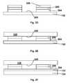
- FIGS. 1A to 1E of the accompanying drawingsare schematic side elevations illustrating various states of one form of the first process of the present invention which produces a first sub-assembly of the invention.
- FIGS. 2A to 2Fare schematic side elevations illustrating various states of one form of the second process of the present invention, this second process producing both first and second sub-assemblies of the invention.
- FIGS. 3A to 3Dare schematic side elevations illustrating various states of a modified form of the second process of the invention shown in FIGS. 2A to 2F , this modified process again producing both first and second sub-assemblies of the invention.
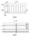
- FIG. 4Ais a schematic side elevation through part of a sheet of FPL used in a third process of the invention for producing a large number of small displays.
- FIG. 4Bis a top plan view of part of the sheet of FPL shown in FIG. 4A and illustrates the manner in which the sheet is kiss cut at an intermediate stage of the third process.
- FIG. 4Cis a schematic side elevation, similar to that of FIG. 4A but at the intermediate stage of the third process illustrated in FIG. 4B .
- FIG. 4Dis a schematic side elevation, similar to those of FIGS. 4A and 4C but at a stage of the third process later than that shown in FIG. 4C .
- FIG. 4Eis a schematic side elevation of a template used in a process for laminating multiple FPL pieces produced by the process shown in FIGS. 4A-4D to backplanes.
- FIG. 4Fis a schematic side elevation, similar to that of FIG. 4E , but showing the template with multiple FPL pieces retained therein.
- FIG. 4Gis a schematic side elevation, similar to that of FIG. 4F , but showing the loaded template being laminated to a sheet comprising multiple backplanes.
- FIG. 4His a schematic side elevation, similar to that of FIG. 4G , showing the structure produced by the lamination.
- FIG. 4Iis a schematic side elevation, similar to that of FIG. 4H , but showing the final structure produced by removal of the template from the structure of FIG. 4H , and prior to the severing of the structure to produce individual displays.
- FIG. 5Ais a schematic top plan view of a sheet of FPL at the first stage of a fourth process of the invention.
- FIG. 5Bis a schematic top plan view, similar to that of FIG. 5A , but at a second stage of the fourth process.
- FIG. 5Cis a schematic cross-section along line C-C in FIG. 5B , but at a third stage of the fourth process.
- loose and tight release sheetsare used in their conventional meaning in the art to indicate the magnitude of the force necessary to peel the relevant release sheet from the layer with which it is in contact, a tight release sheet requiring more force than a loose release sheet.
- a tight release sheetrequiring more force than a loose release sheet.
- the tight release sheetshould have an adhesion at least about 1.5 times, and preferably about 3 times, the adhesion of the loose release sheet.
- the two adhesive layerswill be denoted as “front” and “rear” adhesive layers, these terms denoting the position of the relevant adhesive layer in the final display produced by laminating the sub-assembly to a backplane;
- the front adhesive layeris the adhesive layer lying between the electro-optic medium and the viewing surface of the display (i.e., the surface through which an observer views the display, normally the surface remote from the backplane and regarded as the “front” of the display), while the rear adhesive layer lies on the opposed side of the electro-optic layer from the front adhesive layer, and adjacent the backplane.
- the front adhesive layerlies between the electro-optic layer and the front electrode, while the rear adhesive layer lies between the electro-optic layer and the pixel electrodes.
- the accompanying drawingsare not strictly to scale. In particular, for ease of illustration, the thicknesses of the various layers are greatly exaggerated relative to their lateral dimensions.
- the present inventionis well adapted for the production of thin, flexible, electro-optic displays; typically, the sub-assemblies or front plane laminates which are the products of the processes described below will have thicknesses (measured without the remaining release sheet, which is discarded before the final lamination to a backplane) of about 100 ⁇ m, and can be laminated to flexible backplanes of similar thickness.
- FIGS. 1A-1E , 2 A- 2 F and 3 A- 3 D of the accompanying drawingsillustrate various stages of three different processes of the present invention, all of which ultimately produce first sub-assemblies of the present invention; the second process shown in FIGS. 2A-2F also produces a second sub-assembly of the present invention. Accordingly, it is considered most convenient to first describe the various sub-assemblies of the invention produced by these processes and thereafter to describe the may in which these sub-assemblies are produced by the multi-step processes of the present invention.
- the first sub-assemblies of the present invention produced by the illustrated processesare shown in FIGS. 1D , 1 E, 2 E and 2 F of the accompanying drawings; as explained below, the third process shown in FIGS. 3A-3D ultimately produces first sub-assemblies identical to those shown in FIGS. 2E and 2F .
- the first sub-assemblies shown in FIGS. 1E and 2Fare specialized forms of the inverted front plane laminates described in the aforementioned 2007/0109219; other first sub-assemblies of the present invention (not illustrated) may be specialized forms of the “classic” (i.e., non-inverted) front plane laminates described in the aforementioned U.S. Pat. No. 6,982,178.
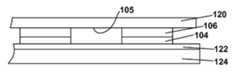
- the first sub-assemblies of the present inventioncomprise a light-transmissive substrate 120 in each of FIGS. 1D , 1 E, 2 E and 2 F.
- the substrate 120is typically a multi-layer structure and usually includes a light-transmissive electrode layer, for example an indium-tin-oxide (ITO) layer, which forms the front electrode of the final display; this electrode layer is not shown separately in the drawings.
- ITOindium-tin-oxide
- substrates 120 lacking electrode layerscan be used, for example in electro-optic displays which are intended to be written using a stylus or similar external electrode.
- the first sub-assemblies of the present inventionfurther comprise a plurality of discrete areas of an electro-optic material ( 104 in FIGS. 1D and 1E , 204 in FIGS. 2E and 2F ) disposed on the substrate 120 .
- the sub-assemblies illustratedhave a substrate (or front) adhesive layer ( 106 in FIGS. 1D and 1E , 206 in FIGS. 2E and 2F ) interposed between the electro-optic material 104 or 204 and the substrate 120 although in some cases this front adhesive layer can be omitted, for example by using an electro-optic material comprising a binder which functions as its own adhesive, as described in the aforementioned U.S. Pat. No. 7,110,164.
- the discrete areas of electro-optic material 104 or 204are separated from each other by gutter areas ( 105 in FIGS. 1D and 1E , 205 in FIGS. 2E and 2F ) free from the electro-optic material and the adhesive layer 106 or 206 .
- gutter areas105 in FIGS. 1D and 1E , 205 in FIGS. 2E and 2F .
- each sub-assemblywould normally have a larger number of discrete areas of electro-optic material; for example, a sub-assembly intended for producing six individual displays might have a 3 ⁇ 2 arrangement of such areas, separated from each other by two parallel gutter areas and a third gutter area extending at right angles to the first two.
- certain sub-assemblies of the present inventioncan be in the form of continuous webs of indefinite length, with a large number of areas of electro-optic material arranged in a two dimensional array and separated from each other by two sets of gutter areas extending in perpendicular directions.
- the first sub-assemblies of the present inventionfurther comprise at least one of an adhesive layer and a release layer on the opposed side of the layer of electro-optic material from the substrate.
- the first sub-assemblies shown in FIGS. 1D and 2Epossess only a release layer 102 on the opposed side of the layer of electro-optic material from the substrate, whereas the sub-assemblies shown in FIGS. 1E and 2F possess both an adhesive layer 122 in contact with the electro-optic layer 104 or 204 and a release layer 124 on the opposed side of the adhesive layer 122 from the electro-optic layer 104 or 204 . Note that in FIG.
- the release layer 102is discontinuous, with separate pieces of release layer 102 just covering the adjacent areas of the electro-optic layer 104 and not extending across the gutter areas 105
- the release layer 102is continuous and extends across the gutter areas 205
- both the adhesive layer 122 and the release layer 124are continuous and extend across the gutter areas 105 or 205 .
- FIG. 2DA second sub-assembly of the present invention is illustrated in FIG. 2D .
- This sub-assemblycomprises a release sheet 102 bearing a plurality of discrete areas of electro-optic material 204 , the discrete areas 204 being separated from each other by gutter areas 205 free from the electro-optic material.
- the second sub-assemblyfurther comprises an adhesive layer 206 on the opposed side of the electro-optic layer from the release sheet 102 and a release layer or sheet 208 on the opposed side of adhesive layer 206 from the release sheet 102 .
- the adhesive layer 206could be omitted.
- the release sheet 208 shown in FIG. 2Dis discontinuous and does not extend across the gutter areas 205 , but second sub-assemblies of the present invention having continuous release sheets similar to 208 can be produced if desired.
- a first method of the present inventionis especially but not exclusively intended for the production of small electro-optic displays.
- an electro-optic mediumis coated or otherwise deposited on to a tight release sheet 102 to form a continuous electro-optic layer 104 .
- a continuous front adhesive layer 106is coated on to a loose release sheet 108 .
- the two resulting sub-assembliesare then laminated to each other with the adhesive layer 106 is contact with the electro-optic layer 104 to produce the structure shown in FIG. 1A .
- These stepsare as described in the aforementioned U.S. Pat. No. 7,110,164, and resulting assembly is a double release sheet as described in the aforementioned 2004/0155857.
- the sheet shown in FIG. 1Ais severed into pieces of appropriate size to form individual displays.
- the cutting of the sheetis conveniently effected by laser cutting, as indicated by lines 110 and 112 in FIG. 1A so as to leave a tab 108 A of the loose release sheet 108 extending outwardly beyond the other layers.
- cutsmay, and typically are, made completely through the sheet to provide any desired apertures or cut-outs in the front adhesive layer 106 and electro-optic layer 104 ; for example, apertures may be cut through the front adhesive and electro-optic layers to provide pre-formed connection apertures as described in the aforementioned application Ser. No.
- a plurality of these pieces(designated 114 in FIG. 1B ) with the loose release sheet 108 removed are then placed, adhesive side up, in a template or jig comprising a thin alignment sheet 116 taped to a laminating tray 118 .
- the alignment sheet 116is disposable and is typically discarded after three or four laminations (as described below), whereas the laminating tray is permanent; this arrangement has the advantage that the alignment sheet 116 can rapidly be changed to enable various parts to be laminated in the same laminator without the need for a plurality of expensive metal templates.
- the alignment sheet 116which is typically formed of a polymeric film, for example poly(ethylene terephthalate) (PET), can be laser cut using the same digital file used to laser cut the pieces 114 .
- the thickness of the alignment sheet 116should be chosen so that the upper (adhesive) surfaces of the pieces 114 extend slightly (about 1-2 mil, 25-51 ⁇ m) above the alignment sheet 116 .
- the pieces 114 held in the template 116 , 118are then laminated to an oversized (i.e., larger than the alignment sheet 116 ) sheet of a front substrate 120 .
- the front substrate 120is a multi-layer structure including an indium-tin-oxide (ITO) layer which forms the front electrode of the final display.
- ITOindium-tin-oxide
- the front substratefurther comprises a removable masking film, which is removed before the final display is placed in use, as described below.
- This front substrate structureis designed to provide the front light-transmissive electrode for the final display.
- the front substrate 120also provides the necessary mechanical support for this thin and relatively fragile front electrode.
- the front substratepreferably provides all necessary water vapor and oxygen barriers, and ultra-violet absorption properties, desirable to protect certain electro-optic layers, especially electrophoretic layers.
- the front substratemay also provide desirable anti-glare properties to the viewing surface of the final display.
- the front substrate 120serves all of these functions while still being thin and flexible enough to enable the formation of a final display sufficiently flexible to be wound around a mandrel of (say) 15 mm diameter.
- the front substrateincludes a masking film; this masking film is provided primarily to increase the thickness of the front substrate so as to facilitate handling of this substrate during the laminations.
- the total thickness of the front substrate as it remains in the final displayi.e., with the masking film removed
- the masking filmis used to add about 2 mil (51 ⁇ m) to this thickness for ease of handling.
- the masking filmalso typically serves to prevent scratching or adhesion of dust or debris to an adjacent anti-glare layer during the laminations.
- FIG. 1Dshows an enlarged view of two of the pieces 114 on the substrate 120 , the pieces 114 and the substrate 120 together forming a first sub-assembly of the present invention, as already described.
- the substrate 120 bearing the pieces 114is then placed on a laser cutter with the pieces 114 facing the laser.
- the laser cutteris then used to cut tooling holes through the front substrate 120 in positions aligned with the positions of the pieces 114 ; these tooling holes will be used to engage the sheet with alignment pins to locate the sheet during a later lamination, as described below.
- tooling holescould be pre-cut in the front substrate 120 before this front substrate is laminated to the pieces 114 , and if such pre-cut tooling holes are provided, they can be engaged with pins provided on the template 116 , 118 to align the front substrate during its lamination to the pieces 114 .
- a rear adhesive layer 122( FIG. 1C ) is coated on to a release sheet 124 , and the exposed surface of the rear adhesive layer is covered by an interleaf (in effect, a further release sheet—not shown in the drawings) which serves to prevent contamination of the surface of the adhesive layer during laser cutting.
- the release layer/adhesive/interleaf “sandwich”is laser cut, with the interleaf facing the laser, to form tooling holes similar to those previously cut through the front substrate, and intended for the same purpose.
- the laser cuttermay also be used to cut other apertures through the adhesive layer required for specific displays; for example, the laser cutter may cut apertures which, in conjunction with corresponding apertures previously cut in the front adhesive and electro-optic layers, will constitute pre-formed connection apertures as described in the aforementioned application Ser. No. 11/682,409.
- the interleafis removed from the rear adhesive layer, 122 , which is then placed, together with its adhering release sheet 124 , on the bed of a laminator, with its tooling holes engaged with alignment pins (not shown) on the laminator, as illustrated in FIG. 1C .
- the tight release sheet 102is peeled from the pieces 114 carried on the substrate 120 , and the tooling holes previously cut in the release sheet 120 are also engaged with the alignment pins on the laminator, such that the exposed surface of the electro-optic layer 104 is facing the rear adhesive layer 122 .
- the two sheetsare them laminated together, thus forming an inverted front plane laminate as described in the aforementioned 2007/0109219.
- FIG. 1CThe tight release sheet 102 is peeled from the pieces 114 carried on the substrate 120 , and the tooling holes previously cut in the release sheet 120 are also engaged with the alignment pins on the laminator, such that the exposed surface of the electro-optic layer 104 is facing the rear adhesive layer
- FIG. 1Eis an enlarged view, similar to that of FIG. 1D and illustrating a portion of substrate 120 bearing two pieces 114 at the same stage as FIG. 1C .
- the structure shown in FIG. 1Econstitutes a first sub-assembly of the present invention.
- the masking filmis typically removed, since it is convenient to remove this film in one piece before the individual displays are separated from each other; however, removal of the masking film can be effected later if desired.
- the next major stepis separation of the sheet into a plurality of pieces of inverted front plane laminate. This separation is effected by laser cutting of the laminated sheet which is held on alignment pins to ensure accurate location of the cuts. The cuts sever the third release sheet 124 , rear adhesive layer 122 and front substrate 120 to produce separate pieces of an inverted front plane laminate which are ready, after removal of the third release sheet 124 , for lamination to backplanes to form the final displays.
- the cutting of the laminated sheetis desirably effected so as to leave a tab of the third release sheet 124 extending beyond the front substrate 120 , adhesive layers 106 and 122 and electro-optic layer 104 ; such a tab facilitates removal of the third release sheet 124 during the production of the final displays.
- a second process of the inventionis primarily intended for use in producing larger displays than the first process described above with reference to FIGS. 1A-1E ; the parts produced by the second process are sufficiently large that loss of the electro-optic material present in gutter areas between adjacent displays can be tolerated.
- the main difference between the first and second processesis that the second process does not make use of a jig to align separate pieces of electro-optic medium on a front substrate; instead, in the second process, a continuous layer of electro-optic material is severed to produce multiple “islands” of electro-optic material separated by gutter areas free from electro-optic material.
- the second process of the present inventionis identical to the first process up to the point shown in FIG. 2A , which is identical to FIG. 1A . However, as may be seen by comparing FIGS. 1B and 2B , the next cutting step differs.
- the cutting step of the second processis effected with the loose release sheet 108 facing the laser cutter and with kiss cutting such that the loose release sheet 108 , the front adhesive layer 106 and the electro-optic layer 104 are severed but the tight release sheet 102 is not.
- any through apertures needed for alignment holes, pre-formed connection apertures or other purposesmay be cut (although this can also be done later, as described below). Since it may in some cases be possible to carry out the entire second process on a roll-to-roll basis, the through apertures formed in this step may include tractor feed holes formed along the side edges of a web of material and serving as alignment holes for later stages of the process.
- the continuous portion of the loose release sheet 108(i.e., the portion of this release sheet covering what will become the gutter areas at later stages of the process) is then removed, either manually or mechanically, thus leaving the structure shown in FIG. 2B , in which “islands” 208 of loose release sheet corresponding to the final displays remain above continuous but severed layers of front adhesive layer 106 and electro-optic layer 104 .
- the next step of the processis removal of the unwanted parts of the front adhesive and electro-optic layers 106 and 104 respectively. This removal can be effected manually, since the front adhesive and electro-optic layers possess sufficient mechanical cohesion that they can be manually rolled up on themselves and removed in large pieces from the underlying tight release sheet 102 . However, as illustrated in FIG.
- a sacrificial sheet 210(which does not need to be tacky) is cold rolled over the islands 208 and the exposed portions of the front adhesive layer 106 .
- the sacrificial sheet 210is then removed, thus removing the portions of the front adhesive layer 106 and electro-optic layer 104 not covered by the islands 208 , and leaving the structure shown in FIG. 2D .
- this structurecomprises a second sub-assembly of the present invention, in which there extend upwardly from the tight release sheet 102 multiple “mesas” comprising the islands 208 of the loose release sheet and similarly sized underlying areas 206 and 204 of the front adhesive layer and electro-optic layer respectively, with the mesas being separated from each other by gutter areas 205 .
- the front adhesive layer 206for example when the electro-optic material can act as its own adhesive.
- each of these mesaswill eventually form a separate display. (In some cases, it may be possible to recycle the portions of the front adhesive layer and electro-optic layer removed on the throwaway sheet 210 in other small displays.)
- the remaining portions 208 of the loose release sheetare peeled from the structure shown in FIG. 2D and the remaining layers of the structure are laminated to a sheet of the front substrate 120 , which can be identical to that used in the first process of the invention as described above, and which can have previously been provided with any apertures needed for engagement with alignment pins etc. during later stages of the process.
- the first sub-assembly of the invention resulting from this laminationis shown in FIG. 2E and has already been described in detail above.
- the sub-assembly shown in FIG. 2Eis very similar to that produced in the first process of the invention following the lamination shown in FIG. 1B and the subsequent laser cutting, the only difference being that in the structure of FIG. 2E the tight release sheet 102 is continuous. Accordingly, the remaining steps of the second process are essentially identical to those of the first. Again, a rear adhesive layer 122 is coated on to a third release sheet 124 , an interleaf is applied over the adhesive layer 122 and any necessary apertures are cut in the resulting structure. The interleaf is then removed, the tight release sheet 102 is removed from the structure of FIG. 2E , and the two resulting films are laminated together to produce the final inverted front plane laminate or sub-assembly shown in FIG. 2F , which is identical to that produced by the first process of the invention.
- FIGS. 3A-3DThe third process of the present invention shown in FIGS. 3A-3D is essentially a variant of the second process described above. As shown in FIGS. 3A and 3B , which are identical to FIGS. 2A and 2B respectively, the third process is identical to the second up to the point shown in FIG. 3B . However, in the next step of the process, instead of the throwaway sheet 210 , a tacky film 310 ( FIG. 3C ) is rolled over, and adheres to, the exposed surfaces of both the loose release sheet 108 and the front adhesive layer 106 .
- the tacky film 310when the tacky film 310 is removed, the remaining loose release sheet 108 , and the unwanted portions of the front adhesive layer 106 and electro-optic 104 are removed therewith, thus producing the structure shown in FIG. 3D ; in effect, the use of the tacky film 310 enables the step from FIG. 2B to FIG. 2C and the subsequent removal of the loose release sheet prior to lamination to the front substrate 120 , to be combined into a single operation.
- the remaining steps of the third processare identical to those of the second.
- the third process of the inventionall removal of unwanted material is effected in sheet form, or in continuous web form if the process is carried out using continuous webs of material. Accordingly, the third process of the invention is very suitable for use on a continuous, roll-to-roll basis.
- the process shown in FIGS. 3A-3D and the subsequent laminations to form the final electro-optic displaysare to be carried out on continuous webs, care must be taken to maintain correct alignment throughout the various steps of the process.
- the “mesas” 204 , 206are produced at known locations on the release sheet 102 . If the structure shown in FIG. 3D is to be subjected to a lamination similar to that shown in FIG.
- the mesasend up aligned with the backplanes, it is necessary to first transfer the mesas to known positions relative to some fixed marker on the front substrate, and then to bring the front substrate bearing the mesas into contact with the backplanes so that the fixed marker on the front substrate is in a known alignment with the backplanes.
- the necessary alignmentsare most readily achieved by providing all the webs with tractor feed holes and ensuring that the webs are driven by common tractor feed devices so that they automatically remain in the desired alignment with each other.
- FIG. 4Aa schematic side elevation through part of a sheet of classic FPL (generally designated 400 ) intended which will be used in a third process of the invention for producing a large number of small displays.
- the sheet 400 of FPL shown in FIG. 4Acomprises an essentially transparent front substrate 402 and a light-transmissive electrically-conductive layer 404 , the latter forming the front electrode in the final electro-optic displays.
- These two layersmay be formed from a commercial ITO-coated PET film.
- the sheet 400further comprises an electro-optic layer 406 , which may be formed of an encapsulated electrophoretic medium (although other types of solid electro-optic medium can also be employed), an adhesive layer 408 and a release sheet 410 .
- the release sheet 410bears on its surface a thin, electrically-conductive layer 412 , which need not be transparent; as described in the aforementioned U.S. Pat. Nos. 6,982,178 and 7,236,292 and as briefly mentioned above, the conductive layer 412 permits testing of the electro-optic layer 406 in the sheet before the sheet is severed to produce individual displays.
- a masking film 414is secured to the surface of the front substrate 402 remote from the electro-optic layer 406 by an adhesive layer 416 .
- the masking film 414serves to protect the exposed surface of the front substrate (which will form the viewing surface of the final display) during the processing steps described below, but is removed before the display is used. In some cases, depending upon the type of front substrate used, and the processing conditions, the masking film and its associated adhesive layer may be omitted.
- FIGS. 4B and 4CThe first step in the third process of the invention is illustrated in FIGS. 4B and 4C , with FIG. 4B being a top plan view of part of the sheet 400 and FIG. 4C being a schematic side elevation similar to that of FIG. 4A .
- the first step of the processis making a series of kiss cuts 418 with a laser, these cuts running parallel to the long edges of the sheet 400 , and extending from the exposed surface of the release sheet 410 through the layers 410 and 412 .
- FIG. 4Bbeing a top plan view of part of the sheet 400
- FIG. 4Cbeing a schematic side elevation similar to that of FIG. 4A .
- the first step of the processis making a series of kiss cuts 418 with a laser, these cuts running parallel to the long edges of the sheet 400 , and extending from the exposed surface of the release sheet 410 through the layers 410 and 412 .
- the kiss cuts 418are in closely-spaced pairs; the pairs of cuts are spaced from adjacent pairs by a distance equal to twice the length of the final FPL pieces, and pairs of cuts adjacent the long edges of the sheet 400 being spaced from the edge by a distance equal to the length of the final FPL pieces.
- the portions of the layers 410 and 412 lying between the closely-spaced pairs of kiss cuts 418are then removed, and the adhesive layer 408 and the electro-optic layer 406 are also mechanically removed between the closely-spaced pairs of kiss cuts 418 , thus leaving a series of parallel “trenches” 420 extending across sheet 400 , as best seen in FIG. 4C .
- the next step in the processis to fill the trenches 420 with strips of conductive adhesive 422 carried on a release sheet 424 , thus placing the conductive adhesive 422 in electrical contact with the conductive layer 404 , as illustrated in FIG. 4D .
- each component 430has an elongate rectangular main section 430 A, where all the layers originally present in the sheet 400 are retained, and a part-circular connection area 430 B, where the release sheet 424 , the conductive adhesive 422 , the conductive layer 404 , the transparent front substrate 402 , the masking film 414 and its associated adhesive layer 416 are present.
- the individual FPL components 430 thus producedmust now be laminated to backplanes.
- the first step in this laminationillustrated in FIG. 4E , is cutting in a template 432 a series of apertures 434 , each just large enough to hold one FPL component 430 .
- a low tack adhesive filmcomprising an adhesive layer 436 on a base layer 438 is then adhered to the cut template 432 so that the adhesive layer 436 is exposed only within the recesses formed by the apertures 434 .
- FIG. 4EThe first step in this lamination, illustrated in FIG. 4E , is cutting in a template 432 a series of apertures 434 , each just large enough to hold one FPL component 430 .
- a low tack adhesive filmcomprising an adhesive layer 436 on a base layer 438 is then adhered to the cut template 432 so that the adhesive layer 436 is exposed only within the recesses formed by the apertures 434 .
- the FPL components 430are placed within the apertures 434 , with the masking film 414 adhered to the adhesive layer 436 , leaving the release sheet 410 exposed; note that the template 432 is made thinner than the FPL components 430 .
- the release sheet 410is peeled from the components 430 (the conductive layer 412 of course being removed with the release sheet 410 ) exposing the adhesive layer 408 , and the release sheet 424 is removed from the conductive adhesive 422 , thus exposing the conductive adhesive 422 ; the remaining layers of the FPL components 430 are still thicker than the template 432 , so that the exposed adhesive layer 408 projects clear of the template 432 .
- the filled templateis then laminated to a backplane assembly 440 ( FIG.
- FIG. 4Gwhich has a plurality of backplane areas, each disposed opposite one of the FPL components 430 .
- the filled template and the backplane assembly 440are laminated to each other using a hot roll laminator schematically indicated at 442 in FIG. 4G .
- the resultant display assembly of the inventionis illustrated in FIG. 4H .
- the backplane areas of the backplane assembly 440are arranged so that each connection area 430 B ( FIG. 4B ) contacts a contact pad on the backplane area, thus establishing electrical contact between the contact pad and the conductive layer 404 ( FIG. 4A or 4 B) via the conductive adhesive 422 .
- the next step of the processis removal of the template 432 , together with the adhesive layer 436 and the base layer 438 is then peeled from the FPL components 430 ; to achieve this peeling, the tackiness of the adhesive layer 436 must be sufficiently low to enable the adhesive layer to be peeled from the masking film 414 without peeling the masking film from the front substrate 402 .
- the display assembly obtained by removal of the template 432 , the adhesive layer 436 and the base layer 438is a display assembly of the present invention.
- FIGS. 5A-5Cillustrate a fourth process of the present invention for producing a display assembly.
- the process of FIGS. 5A-5Cbegins with a sheet 400 of FPL identical (except perhaps in size) to that used as the starting material in the third process, as described above with reference to FIG. 4A .
- the fourth processdoes not use a template but laminates the entire sheet 400 to the backplane assembly, after appropriate cutting of the sheet 400 to enable post-lamination separation of the FPL components from the remaining portions of the sheet 400 .
- the first step of the fourth processis kiss cutting (indicated by broken lines) of the release sheet 410 and the conductive layer 412 disposed thereon to define a series of spaced individual FPL pieces (or components), generally designated 530 each comprising an elongate rectangular main section 530 A and a part-circular connection area 530 B.
- the sheet 400is completely severed by through cuts along the periphery of the each FPL component 530 , except that two small sections 550 A and 550 B remain uncut to hold the components 530 within the sheet 400 .
- the remaining broken lines in FIG. 5Bindicate that only the kiss cuts through the release sheet 410 and the conductive layer 412 are present in sections 550 A and 550 B and along the line dividing the sections 530 A and 530 B of the components 530 .
- connection areas 530 Bare then covered (as illustrated in FIG. 5C ) with pre-cut pieces of a conductive adhesive layer 522 carried on a release sheet 524 .
- the release sheet 410 and the conductive layer 412are then removed from the main sections 530 A and the release 524 is removed from the connection areas 530 B; outside the FPL components 530 , the release sheet 410 remains in position.
- the sheet 400is then laminated to an appropriate backplane assembly (not shown) using a hot roll laminator in a manner exactly analogous to the lamination described with reference to FIG. 4G , except that no template is used.
- the sheet 400may of course be mounted upon a suitable support member during the lamination, and any conventional means, such as pins on the support member interacting with apertures cut in the sheet 400 , may be used to align the sheet with the support member.
- This laminationresults in the main sections 530 A of the FPL components becoming adhered to backplane areas and the connections areas 530 B being in electrical contact with contact pads (not shown) via the conductive adhesive layer 522 , in a manner exactly analogous to lamination described above with reference to FIG. 4G .
- the portion of the sheet 400 not forming part of the FPL components 530is next peeled from the backplane assembly, with the two small sections 550 A and 550 B ( FIG. 5B ) tearing as the sheet 400 is peeled.
- the resulting assemblyis very similar to that illustrated in FIG. 4I , and again the final step is typically severing the backplane assembly to produce a plurality of discrete displays.
- the third and fourth processes of the inventionproduce the same final product, as illustrated in FIG. 4I .
- the choice between the third and fourth processesdepends upon a number of factors, including the physical characteristics of the FPL and the size of the displays being created. For any given FPL, there will be a minimum width of gutter area in the fourth process which will permit ready peeling of the gutter area after lamination. The fourth process inevitably wastes some FPL (that present in the gutter areas), and if the displays being produced are very small, this wastage may become uneconomic. Furthermore, if the displays are very small, difficulty may be encountered in placing the conductive adhesive in the connection areas 530 B in the fourth process. Accordingly, in general the third process may be better adopted for very small displays and the fourth process for larger displays.
- the processes of the present inventioncan be carried out with any electro-optic layer which has solid external surfaces to which adhesive layers and release sheets can adhere and sufficient mechanical cohesion to permit the necessary manipulation of films containing the electro-optic layer. Accordingly, the present processes can be carried out using any of the types of electro-optic media described above.
- the present methodscan make use of rotating bichromal member, electrochromic or electrophoretic media, and in the last case the electrophoretic media may be of the encapsulated, polymer-dispersed or microcell types.
Landscapes
- Physics & Mathematics (AREA)
- Nonlinear Science (AREA)
- Chemical Kinetics & Catalysis (AREA)
- Health & Medical Sciences (AREA)
- Electrochemistry (AREA)
- Molecular Biology (AREA)
- Chemical & Material Sciences (AREA)
- Life Sciences & Earth Sciences (AREA)
- General Physics & Mathematics (AREA)
- Optics & Photonics (AREA)
- Engineering & Computer Science (AREA)
- Mechanical Engineering (AREA)
- Electrochromic Elements, Electrophoresis, Or Variable Reflection Or Absorption Elements (AREA)
Abstract
Description
- (a) copending application Ser. No. 10/605,024, filed Sep. 2, 2003 (Publication No. 2004/0155857);
- (b) application Ser. No. 10/904,063, filed Oct. 21, 2004 (now U.S. Pat. No. 7,110,164), which is a continuation-in-part of the aforementioned application Ser. No. 10/605,024;
- (c) application Ser. No. 11/307,297, filed Jan. 31, 2006, which is a divisional of the aforementioned application Ser. No. 10/904,063;
- (d) copending application Ser. No. 11/550,114, filed Oct. 17, 2006 (Publication No. 2007/0109219) and claiming benefit of Application Ser. No. 60/596,743, filed Oct. 18, 2005 and of Application Ser. No. 60/596,799, filed Oct. 21, 2005;
- (e) copending application Ser. No. 11/612,732, filed Dec. 19, 2006 (Publication No. 2007/0152956) and claiming benefit of Application Ser. No. 60/597,801, filed Dec. 20, 2005;
- (f) copending application Ser. No. 11/682,409, filed Mar. 6, 2007 and claiming benefit of Application Ser. No. 60/767,171, filed Mar. 8, 2006; and
- (g) copending application Ser. No. 11/561,536, filed Nov. 20, 2006 (Publication No. 2007/0153361) and claiming benefit of Application Ser. No. 60/597,279, filed Nov. 21, 2005, and of Application Ser. No. 60/744,022, filed Mar. 31, 2006.
- a light-transmissive substrate;
- a plurality of discrete areas of an electro-optic material disposed on the substrate, the discrete areas being separated from each other by gutter areas essentially free from the electro-optic material; and
- on the opposed side of the areas of electro-optic material from the substrate, at least one of an adhesive layer and a release layer peelable from the sub-assembly without substantial damage thereto.
- a release sheet;
- a plurality of discrete areas of an electro-optic material disposed on the substrate, the discrete areas being separated from each other by gutter areas essentially free from the electro-optic material,
- the release sheet being peelable from the electro-optic material without substantial damage thereto; and
- on the opposed side of the areas of electro-optic material from the substrate, at least one of an adhesive layer and a release layer, the release layer being peelable from the electro-optic material or adhesive layer with which it is in contact without substantial damage thereto.
- forming a plurality of components, each component comprising a layer of electro-optic material and a release layer peelable from the layer of electro-optic material without substantial damage thereto;
- disposing the plurality of components on a support surface, the components being spaced from each other, with the layer of electro-optic material facing away from the support surface; and
- contacting the disposed plurality of components with a light-transmissive substrate under conditions effective to cause the plurality of components to adhere to the substrate.
- forming a layer of electro-optic material on a release sheet;
- severing the layer of electro-optic material on the release sheet to define a plurality of discrete areas separated from each other by gutter areas;
- removing the layer of electro-optic material from the gutter areas while leaving the electro-optic material on the release sheet in the plurality of discrete areas; and
- after removal of the layer of electro-optic material from the gutter areas, adhering a light-transmissive substrate to the electro-optic material in the plurality of discrete areas.
- a backplane assembly comprising a plurality of spaced backplane areas, each backplane area comprising a plurality of electrodes, the backplane areas being separated by gutter areas free from electrodes;
- an adhesive layer overlying the plurality of spaced backplane areas; and
- a layer of a solid electro-optic medium overlying the adhesive layer in the plurality of spaced backplane areas.
- forming a plurality of components, each component comprising a layer of solid electro-optic material and an adhesive layer;
- disposing the plurality of components on a support surface, the components being spaced from each other, with the adhesive layer facing away from the support surface; and
- contacting the disposed plurality of components with a backplane assembly comprising a plurality of spaced backplane areas, each backplane area comprising a plurality of electrodes, the backplane areas being separated by gutter areas free from electrodes, the contacting being effected under conditions effective to cause the plurality of components to adhere to the backplane areas of the backplane assembly.
- forming an electro-optic sheet comprising, in this order, a layer of solid electro-optic material, an adhesive layer, and a release sheet;
- partially severing the electro-optic sheet to define a plurality of discrete components separated from each other by gutter areas, the layer of solid electro-optic material, adhesive layer, and release sheet being severed along at least the major portion of the periphery of each component;
- removing the release sheet from the adhesive layer in the plurality of discrete components but leaving the release sheet in contact with the adhesive layer in the gutter areas; and
- contacting the electro-optic sheet with a backplane assembly comprising a plurality of spaced backplane areas, each backplane area comprising a plurality of electrodes, the contacting being effected such that each component becomes aligned with one of the spaced backplane areas under conditions effective to cause the plurality of components to adhere to the backplane areas of the backplane assembly, thereby producing the display assembly.
Claims (25)
Priority Applications (1)
| Application Number | Priority Date | Filing Date | Title |
|---|---|---|---|
| US12/550,470US8049947B2 (en) | 2002-06-10 | 2009-08-31 | Components and methods for use in electro-optic displays |
Applications Claiming Priority (11)
| Application Number | Priority Date | Filing Date | Title |
|---|---|---|---|
| US31930002P | 2002-06-10 | 2002-06-10 | |
| US32018603P | 2003-05-12 | 2003-05-12 | |
| US10/249,957US6982178B2 (en) | 2002-06-10 | 2003-05-22 | Components and methods for use in electro-optic displays |
| US10/907,065US7236292B2 (en) | 2002-06-10 | 2005-03-18 | Components and methods for use in electro-optic displays |
| US59533205P | 2005-06-23 | 2005-06-23 | |
| US59595705P | 2005-08-19 | 2005-08-19 | |
| US11/426,077US7554712B2 (en) | 2005-06-23 | 2006-06-23 | Edge seals for, and processes for assembly of, electro-optic displays |
| US82625806P | 2006-09-20 | 2006-09-20 | |
| US11/747,546US7443571B2 (en) | 2002-06-10 | 2007-05-11 | Components and methods for use in electro-optic displays |
| US11/850,831US7583427B2 (en) | 2002-06-10 | 2007-09-06 | Components and methods for use in electro-optic displays |
| US12/550,470US8049947B2 (en) | 2002-06-10 | 2009-08-31 | Components and methods for use in electro-optic displays |
Related Parent Applications (1)
| Application Number | Title | Priority Date | Filing Date |
|---|---|---|---|
| US11/850,831Continuation-In-PartUS7583427B2 (en) | 2002-06-10 | 2007-09-06 | Components and methods for use in electro-optic displays |
Publications (2)
| Publication Number | Publication Date |
|---|---|
| US20100165446A1 US20100165446A1 (en) | 2010-07-01 |
| US8049947B2true US8049947B2 (en) | 2011-11-01 |
Family
ID=42284611
Family Applications (1)
| Application Number | Title | Priority Date | Filing Date |
|---|---|---|---|
| US12/550,470Expired - Fee RelatedUS8049947B2 (en) | 2002-06-10 | 2009-08-31 | Components and methods for use in electro-optic displays |
Country Status (1)
| Country | Link |
|---|---|
| US (1) | US8049947B2 (en) |
Cited By (42)
| Publication number | Priority date | Publication date | Assignee | Title |
|---|---|---|---|---|
| US8270064B2 (en) | 2009-02-09 | 2012-09-18 | E Ink Corporation | Electrophoretic particles, and processes for the production thereof |
| US8446664B2 (en) | 2010-04-02 | 2013-05-21 | E Ink Corporation | Electrophoretic media, and materials for use therein |
| US8553012B2 (en) | 2001-03-13 | 2013-10-08 | E Ink Corporation | Apparatus for displaying drawings |
| US8754859B2 (en) | 2009-10-28 | 2014-06-17 | E Ink Corporation | Electro-optic displays with touch sensors and/or tactile feedback |
| US9293511B2 (en) | 1998-07-08 | 2016-03-22 | E Ink Corporation | Methods for achieving improved color in microencapsulated electrophoretic devices |
| WO2016191673A1 (en) | 2015-05-27 | 2016-12-01 | E Ink Corporation | Methods and circuitry for driving display devices |
| US9671635B2 (en) | 2014-02-07 | 2017-06-06 | E Ink Corporation | Electro-optic display backplane structures with drive components and pixel electrodes on opposed surfaces |
| US9715155B1 (en) | 2013-01-10 | 2017-07-25 | E Ink Corporation | Electrode structures for electro-optic displays |
| US9726957B2 (en) | 2013-01-10 | 2017-08-08 | E Ink Corporation | Electro-optic display with controlled electrochemical reactions |
| US9835925B1 (en) | 2015-01-08 | 2017-12-05 | E Ink Corporation | Electro-optic displays, and processes for the production thereof |
| US10175550B2 (en) | 2014-11-07 | 2019-01-08 | E Ink Corporation | Applications of electro-optic displays |
| US10190743B2 (en) | 2012-04-20 | 2019-01-29 | E Ink Corporation | Illumination systems for reflective displays |
| WO2019089042A1 (en) | 2017-11-03 | 2019-05-09 | E Ink Corporation | Processes for producing electro-optic displays |
| US10317767B2 (en) | 2014-02-07 | 2019-06-11 | E Ink Corporation | Electro-optic display backplane structure with drive components and pixel electrodes on opposed surfaces |
| US10324577B2 (en) | 2017-02-28 | 2019-06-18 | E Ink Corporation | Writeable electrophoretic displays including sensing circuits and styli configured to interact with sensing circuits |
| US10446585B2 (en) | 2014-03-17 | 2019-10-15 | E Ink Corporation | Multi-layer expanding electrode structures for backplane assemblies |
| US10466565B2 (en) | 2017-03-28 | 2019-11-05 | E Ink Corporation | Porous backplane for electro-optic display |
| US10495941B2 (en) | 2017-05-19 | 2019-12-03 | E Ink Corporation | Foldable electro-optic display including digitization and touch sensing |
| US10527899B2 (en) | 2016-05-31 | 2020-01-07 | E Ink Corporation | Backplanes for electro-optic displays |
| US10573257B2 (en) | 2017-05-30 | 2020-02-25 | E Ink Corporation | Electro-optic displays |
| WO2020060960A1 (en) | 2018-09-17 | 2020-03-26 | E Ink Corporation | Backplanes with hexagonal and triangular electrodes |
| WO2020097462A1 (en) | 2018-11-09 | 2020-05-14 | E Ink Corporation | Electro-optic displays |
| WO2020122917A1 (en) | 2018-12-13 | 2020-06-18 | E Ink Corporation | Illumination systems for reflective displays |
| US10824042B1 (en) | 2017-10-27 | 2020-11-03 | E Ink Corporation | Electro-optic display and composite materials having low thermal sensitivity for use therein |
| US10882042B2 (en) | 2017-10-18 | 2021-01-05 | E Ink Corporation | Digital microfluidic devices including dual substrates with thin-film transistors and capacitive sensing |
| US11175561B1 (en) | 2018-04-12 | 2021-11-16 | E Ink Corporation | Electrophoretic display media with network electrodes and methods of making and using the same |
| WO2021247470A1 (en) | 2020-06-03 | 2021-12-09 | E Ink Corporation | Foldable electrophoretic display module including non-conductive support plate |
| US11397361B2 (en) | 2015-06-29 | 2022-07-26 | E Ink Corporation | Method for mechanical and electrical connection to display electrodes |
| US11404013B2 (en) | 2017-05-30 | 2022-08-02 | E Ink Corporation | Electro-optic displays with resistors for discharging remnant charges |
| US11467466B2 (en) | 2012-04-20 | 2022-10-11 | E Ink Corporation | Illumination systems for reflective displays |
| US11511096B2 (en) | 2018-10-15 | 2022-11-29 | E Ink Corporation | Digital microfluidic delivery device |
| US11521565B2 (en) | 2018-12-28 | 2022-12-06 | E Ink Corporation | Crosstalk reduction for electro-optic displays |
| US11537024B2 (en) | 2018-12-30 | 2022-12-27 | E Ink California, Llc | Electro-optic displays |
| WO2023167901A1 (en) | 2022-03-01 | 2023-09-07 | E Ink California, Llc | Temperature compensation in electro-optic displays |
| US11892739B2 (en) | 2020-02-07 | 2024-02-06 | E Ink Corporation | Electrophoretic display layer with thin film top electrode |
| US11935495B2 (en) | 2021-08-18 | 2024-03-19 | E Ink Corporation | Methods for driving electro-optic displays |
| US12190730B2 (en) | 2022-02-28 | 2025-01-07 | E Ink Corporation | Parking space management system |
| WO2025049362A1 (en) | 2023-08-30 | 2025-03-06 | E Ink Corporation | An electro-optic device having electrophoretic medium comprising an organic electroactive compound |
| WO2025096260A1 (en) | 2023-10-31 | 2025-05-08 | E Ink Corporation | A color electro-optic display comprising a light fastness additive |
| US12313951B2 (en) | 2016-06-10 | 2025-05-27 | E Ink Corporation | Electro-optic display apparatus |
| WO2025147504A1 (en) | 2024-01-05 | 2025-07-10 | E Ink Corporation | An electrophoretic medium comprising particles having a pigment core and a polymeric shell |
| WO2025151355A1 (en) | 2024-01-08 | 2025-07-17 | E Ink Corporation | Electrophoretic device having an adhesive layer comprising conductive filler particles and a polymeric dispersant |
Families Citing this family (3)
| Publication number | Priority date | Publication date | Assignee | Title |
|---|---|---|---|---|
| JP2010114106A (en)* | 2008-11-04 | 2010-05-20 | Canon Inc | Transfer method of functional region, led array, led printer head, and led printer |
| US9443453B2 (en)* | 2013-06-14 | 2016-09-13 | Green Light Innovations | Illuminated display board having an angled light source |
| US10926256B2 (en)* | 2017-07-12 | 2021-02-23 | Sharp Life Science (Eu) Limited | Housing for simple assembly of an EWOD device |
Citations (261)
| Publication number | Priority date | Publication date | Assignee | Title |
|---|---|---|---|---|
| US3391014A (en) | 1964-04-27 | 1968-07-02 | Harris Intertype Corp | Liquid development of electrostatic images |
| US3668106A (en) | 1970-04-09 | 1972-06-06 | Matsushita Electric Industrial Co Ltd | Electrophoretic display device |
| US3756693A (en) | 1970-12-21 | 1973-09-04 | Matsushita Electric Industrial Co Ltd | Electrophoretic display device |
| US3767392A (en) | 1970-04-15 | 1973-10-23 | Matsushita Electric Industrial Co Ltd | Electrophoretic light image reproduction process |
| US3772013A (en) | 1971-01-06 | 1973-11-13 | Xerox Corp | Photoelectrophoretic imaging process employing electrically photosensitive particles and inert particles |
| US3792308A (en) | 1970-06-08 | 1974-02-12 | Matsushita Electric Industrial Co Ltd | Electrophoretic display device of the luminescent type |
| US3870517A (en) | 1969-10-18 | 1975-03-11 | Matsushita Electric Industrial Co Ltd | Color image reproduction sheet employed in photoelectrophoretic imaging |
| US3892568A (en) | 1969-04-23 | 1975-07-01 | Matsushita Electric Industrial Co Ltd | Electrophoretic image reproduction process |
| US3959906A (en) | 1973-11-14 | 1976-06-01 | J. Robert Norris, Jr. | Message display system |
| US4093534A (en) | 1974-02-12 | 1978-06-06 | Plessey Handel Und Investments Ag | Working fluids for electrophoretic image display devices |
| US4160257A (en) | 1978-07-17 | 1979-07-03 | Dennison Manufacturing Company | Three electrode system in the generation of electrostatic images |
| US4272596A (en) | 1979-06-01 | 1981-06-09 | Xerox Corporation | Electrophoretic display device |
| US4418346A (en) | 1981-05-20 | 1983-11-29 | Batchelder J Samuel | Method and apparatus for providing a dielectrophoretic display of visual information |
| US4522472A (en) | 1982-02-19 | 1985-06-11 | North American Philips Corporation | Electrophoretic image display with reduced drives and leads |
| US4550982A (en) | 1981-11-09 | 1985-11-05 | Nippon Electric Co., Ltd. | All-solid-state display including an organic electrochromic layer with ion donor/acceptor |
| US4602263A (en) | 1984-09-04 | 1986-07-22 | Polaroid Corporation | Thermal imaging method |
| US4655897A (en) | 1984-11-13 | 1987-04-07 | Copytele, Inc. | Electrophoretic display panels and associated methods |
| US4681403A (en) | 1981-07-16 | 1987-07-21 | U.S. Philips Corporation | Display device with micromechanical leaf spring switches |
| US4703573A (en) | 1985-02-04 | 1987-11-03 | Montgomery John W | Visual and audible activated work and method of forming same |
| US4742345A (en) | 1985-11-19 | 1988-05-03 | Copytele, Inc. | Electrophoretic display panel apparatus and methods therefor |
| US4746917A (en) | 1986-07-14 | 1988-05-24 | Copytele, Inc. | Method and apparatus for operating an electrophoretic display between a display and a non-display mode |
| US4902108A (en) | 1986-03-31 | 1990-02-20 | Gentex Corporation | Single-compartment, self-erasing, solution-phase electrochromic devices, solutions for use therein, and uses thereof |
| US5250938A (en) | 1990-12-19 | 1993-10-05 | Copytele, Inc. | Electrophoretic display panel having enhanced operation |
| US5276438A (en) | 1991-08-29 | 1994-01-04 | Copytele, Inc. | Electrophoretic display panel with internal mesh background screen |
| US5288433A (en) | 1988-04-29 | 1994-02-22 | Jim Stevens | Electrochromic device and a method to manufacture the same |
| US5293528A (en) | 1992-02-25 | 1994-03-08 | Copytele, Inc. | Electrophoretic display panel and associated methods providing single pixel erase capability |
| US5378404A (en) | 1991-04-22 | 1995-01-03 | Alliedsignal Inc. | Process for forming dispersions or solutions of electrically conductive conjugated polymers in a polymeric or liquid phase |
| US5402145A (en) | 1993-02-17 | 1995-03-28 | Copytele, Inc. | Electrophoretic display panel with arc driven individual pixels |
| US5412398A (en) | 1992-02-25 | 1995-05-02 | Copytele, Inc. | Electrophoretic display panel and associated methods for blinking displayed characters |
| US5467107A (en) | 1993-10-01 | 1995-11-14 | Copytele, Inc. | Electrophoretic display panel with selective character addressability |
| US5485176A (en) | 1991-11-21 | 1996-01-16 | Kabushiki Kaisha Sega Enterprises | Information display system for electronically reading a book |
| US5484292A (en) | 1989-08-21 | 1996-01-16 | Mctaggart; Stephen I. | Apparatus for combining audio and visual indicia |
| US5548282A (en) | 1993-05-05 | 1996-08-20 | Pricer Ab | Electronic shelf edge price display system |
| US5745094A (en) | 1994-12-28 | 1998-04-28 | International Business Machines Corporation | Electrophoretic display |
| US5760761A (en) | 1995-12-15 | 1998-06-02 | Xerox Corporation | Highlight color twisting ball display |
| US5777782A (en) | 1996-12-24 | 1998-07-07 | Xerox Corporation | Auxiliary optics for a twisting ball display |
| US5800950A (en) | 1995-03-16 | 1998-09-01 | Kabushiki Kaisha Toshiba | Recording medium |
| US5808783A (en) | 1996-06-27 | 1998-09-15 | Xerox Corporation | High reflectance gyricon display |
| US5825526A (en) | 1996-04-24 | 1998-10-20 | Minnesota Mining And Manufacturing Company | Tape for use in manufacturing electrochromic devices |
| US5930026A (en) | 1996-10-25 | 1999-07-27 | Massachusetts Institute Of Technology | Nonemissive displays and piezoelectric power supplies therefor |
| US5961804A (en) | 1997-03-18 | 1999-10-05 | Massachusetts Institute Of Technology | Microencapsulated electrophoretic display |
| US6017584A (en) | 1995-07-20 | 2000-01-25 | E Ink Corporation | Multi-color electrophoretic displays and materials for making the same |
| US6025896A (en) | 1997-10-09 | 2000-02-15 | Brother Kogyo Kabushiki Kaisha | Display device |
| US6054071A (en) | 1998-01-28 | 2000-04-25 | Xerox Corporation | Poled electrets for gyricon-based electric-paper displays |
| US6055091A (en) | 1996-06-27 | 2000-04-25 | Xerox Corporation | Twisting-cylinder display |
| US6067185A (en) | 1997-08-28 | 2000-05-23 | E Ink Corporation | Process for creating an encapsulated electrophoretic display |
| US6097531A (en) | 1998-11-25 | 2000-08-01 | Xerox Corporation | Method of making uniformly magnetized elements for a gyricon display |
| US6105290A (en) | 1993-05-25 | 2000-08-22 | Coates Signco Pty. Limited | Display device |
| US6118426A (en) | 1995-07-20 | 2000-09-12 | E Ink Corporation | Transducers and indicators having printed displays |
| US6117368A (en) | 1993-04-21 | 2000-09-12 | Copytele, Inc. | Black and white electrophoretic particles and method of manufacture |
| US6120588A (en) | 1996-07-19 | 2000-09-19 | E Ink Corporation | Electronically addressable microencapsulated ink and display thereof |
| US6120839A (en) | 1995-07-20 | 2000-09-19 | E Ink Corporation | Electro-osmotic displays and materials for making the same |
| US6124851A (en) | 1995-07-20 | 2000-09-26 | E Ink Corporation | Electronic book with multiple page displays |
| US6128124A (en) | 1998-10-16 | 2000-10-03 | Xerox Corporation | Additive color electric paper without registration or alignment of individual elements |
| US6130774A (en) | 1998-04-27 | 2000-10-10 | E Ink Corporation | Shutter mode microencapsulated electrophoretic display |
| US6137467A (en) | 1995-01-03 | 2000-10-24 | Xerox Corporation | Optically sensitive electric paper |
| US6144361A (en) | 1998-09-16 | 2000-11-07 | International Business Machines Corporation | Transmissive electrophoretic display with vertical electrodes |
| US6147791A (en) | 1998-11-25 | 2000-11-14 | Xerox Corporation | Gyricon displays utilizing rotating elements and magnetic latching |
| US6151153A (en) | 1998-06-16 | 2000-11-21 | Photon Dynamics, Inc. | Modulator transfer process and assembly |
| US6177921B1 (en) | 1997-08-28 | 2001-01-23 | E Ink Corporation | Printable electrode structures for displays |
| US6184856B1 (en) | 1998-09-16 | 2001-02-06 | International Business Machines Corporation | Transmissive electrophoretic display with laterally adjacent color cells |
| US6204953B1 (en) | 1997-10-07 | 2001-03-20 | Optical Coating Laboratory, Inc. | Protective coating materials for electrochromic devices |
| US6225971B1 (en) | 1998-09-16 | 2001-05-01 | International Business Machines Corporation | Reflective electrophoretic display with laterally adjacent color cells using an absorbing panel |
| US6232950B1 (en) | 1997-08-28 | 2001-05-15 | E Ink Corporation | Rear electrode structures for displays |
| US6241921B1 (en) | 1998-05-15 | 2001-06-05 | Massachusetts Institute Of Technology | Heterogeneous display elements and methods for their fabrication |
| US6249271B1 (en) | 1995-07-20 | 2001-06-19 | E Ink Corporation | Retroreflective electrophoretic displays and materials for making the same |
| US6252564B1 (en) | 1997-08-28 | 2001-06-26 | E Ink Corporation | Tiled displays |
| US6262706B1 (en) | 1995-07-20 | 2001-07-17 | E Ink Corporation | Retroreflective electrophoretic displays and materials for making the same |
| US6262833B1 (en) | 1998-10-07 | 2001-07-17 | E Ink Corporation | Capsules for electrophoretic displays and methods for making the same |
| US6271823B1 (en) | 1998-09-16 | 2001-08-07 | International Business Machines Corporation | Reflective electrophoretic display with laterally adjacent color cells using a reflective panel |
| US6301038B1 (en) | 1997-02-06 | 2001-10-09 | University College Dublin | Electrochromic system |
| US6300932B1 (en) | 1997-08-28 | 2001-10-09 | E Ink Corporation | Electrophoretic displays with luminescent particles and materials for making the same |
| US6312971B1 (en) | 1999-08-31 | 2001-11-06 | E Ink Corporation | Solvent annealing process for forming a thin semiconductor film with advantageous properties |
| US6312304B1 (en) | 1998-12-15 | 2001-11-06 | E Ink Corporation | Assembly of microencapsulated electronic displays |
| US6323989B1 (en) | 1996-07-19 | 2001-11-27 | E Ink Corporation | Electrophoretic displays using nanoparticles |
| US20010046399A1 (en) | 2000-03-31 | 2001-11-29 | Brother Kogyo Kabushiki Kaisha | Image forming device and ink sheet cartridge mounted on the image forming device |
| US6327072B1 (en) | 1999-04-06 | 2001-12-04 | E Ink Corporation | Microcell electrophoretic displays |
| US6330054B1 (en) | 1998-09-30 | 2001-12-11 | Brother Kogyo Kabushiki Kaisha | Image-forming method and image-forming apparatus on recording medium including microcapsules |
| US6337761B1 (en) | 1999-10-01 | 2002-01-08 | Lucent Technologies Inc. | Electrophoretic display and method of making the same |
| EP1099207B1 (en) | 1998-07-22 | 2002-03-27 | E-Ink Corporation | Electronic display |
| JP2002098945A (en) | 2000-09-21 | 2002-04-05 | Seiko Epson Corp | Liquid crystal device, light shielding sheet for liquid crystal device, and method of manufacturing liquid crystal device |
| US6377387B1 (en) | 1999-04-06 | 2002-04-23 | E Ink Corporation | Methods for producing droplets for use in capsule-based electrophoretic displays |
| US6376828B1 (en) | 1998-10-07 | 2002-04-23 | E Ink Corporation | Illumination system for nonemissive electronic displays |
| US6392786B1 (en) | 1999-07-01 | 2002-05-21 | E Ink Corporation | Electrophoretic medium provided with spacers |
| US20020061451A1 (en) | 2000-09-14 | 2002-05-23 | Dai Nippon Printing Co., Ltd. | Intermediate transfer recording medium and method for image formation |
| US20020060321A1 (en) | 2000-07-14 | 2002-05-23 | Kazlas Peter T. | Minimally- patterned, thin-film semiconductor devices for display applications |
| US6400492B1 (en) | 1999-06-11 | 2002-06-04 | Ricoh Company Limited | Electrophoretic display liquid, and electrophoretic display medium, method and device using the liquid |
| US6413790B1 (en) | 1999-07-21 | 2002-07-02 | E Ink Corporation | Preferred methods for producing electrical circuit elements used to control an electronic display |
| US20020090980A1 (en) | 2000-12-05 | 2002-07-11 | Wilcox Russell J. | Displays for portable electronic apparatus |
| US20020106874A1 (en) | 1998-07-03 | 2002-08-08 | Masaaki Iwane | Crystal growth process, semiconductor device, and its production process |
| US6445489B1 (en) | 1998-03-18 | 2002-09-03 | E Ink Corporation | Electrophoretic displays and systems for addressing such displays |
| US6459418B1 (en) | 1995-07-20 | 2002-10-01 | E Ink Corporation | Displays combining active and non-active inks |
| US6473072B1 (en) | 1998-05-12 | 2002-10-29 | E Ink Corporation | Microencapsulated electrophoretic electrostatically-addressed media for drawing device applications |
| US6480182B2 (en) | 1997-03-18 | 2002-11-12 | Massachusetts Institute Of Technology | Printable electronic display |
| US6498114B1 (en) | 1999-04-09 | 2002-12-24 | E Ink Corporation | Method for forming a patterned semiconductor film |
| US6504524B1 (en) | 2000-03-08 | 2003-01-07 | E Ink Corporation | Addressing methods for displays having zero time-average field |
| US6506438B2 (en) | 1998-12-15 | 2003-01-14 | E Ink Corporation | Method for printing of transistor arrays on plastic substrates |
| US6512354B2 (en) | 1998-07-08 | 2003-01-28 | E Ink Corporation | Method and apparatus for sensing the state of an electrophoretic display |
| US6515649B1 (en) | 1995-07-20 | 2003-02-04 | E Ink Corporation | Suspended particle displays and materials for making the same |
| US6515790B2 (en) | 2000-01-28 | 2003-02-04 | Minolta Co., Ltd. | Reversible image display medium and image display method |
| US6518949B2 (en) | 1998-04-10 | 2003-02-11 | E Ink Corporation | Electronic displays using organic-based field effect transistors |
| US6531997B1 (en) | 1999-04-30 | 2003-03-11 | E Ink Corporation | Methods for addressing electrophoretic displays |
| US6538801B2 (en) | 1996-07-19 | 2003-03-25 | E Ink Corporation | Electrophoretic displays using nanoparticles |
| US6545291B1 (en) | 1999-08-31 | 2003-04-08 | E Ink Corporation | Transistor design for use in the construction of an electronically driven display |
| EP1145072B1 (en) | 1998-06-22 | 2003-05-07 | E-Ink Corporation | Method of addressing microencapsulated display media |
| US20030102858A1 (en) | 1998-07-08 | 2003-06-05 | E Ink Corporation | Method and apparatus for determining properties of an electrophoretic display |
| US6580545B2 (en) | 2001-04-19 | 2003-06-17 | E Ink Corporation | Electrochromic-nanoparticle displays |
| US20030179436A1 (en) | 2000-03-03 | 2003-09-25 | Rong-Chang Liang | Electrophoretic display and novel process for its manufacture |
| US6639578B1 (en) | 1995-07-20 | 2003-10-28 | E Ink Corporation | Flexible displays |
| US6657772B2 (en) | 2001-07-09 | 2003-12-02 | E Ink Corporation | Electro-optic display and adhesive composition for use therein |
| US6661563B2 (en) | 2000-01-31 | 2003-12-09 | Fujitsu Limited | Sheet-shaped display, sphere-like resin body, and micro-capsule |
| US6664944B1 (en) | 1995-07-20 | 2003-12-16 | E-Ink Corporation | Rear electrode structures for electrophoretic displays |
| US6671030B2 (en) | 2000-04-27 | 2003-12-30 | Seiko Epson Corporation | Electro-optical device including a contiguous sealing member and method for manufacturing the same |
| US6672921B1 (en) | 2000-03-03 | 2004-01-06 | Sipix Imaging, Inc. | Manufacturing process for electrophoretic display |
| USD485294S1 (en) | 1998-07-22 | 2004-01-13 | E Ink Corporation | Electrode structure for an electronic display |
| US6680517B2 (en) | 2000-08-23 | 2004-01-20 | Tdk Corporation | Anisotropic conductive film, production method thereof, and display apparatus using anisotropic film |
| US6693620B1 (en) | 1999-05-03 | 2004-02-17 | E Ink Corporation | Threshold addressing of electrophoretic displays |
| US6704133B2 (en) | 1998-03-18 | 2004-03-09 | E-Ink Corporation | Electro-optic display overlays and systems for addressing such displays |
| US6710540B1 (en) | 1995-07-20 | 2004-03-23 | E Ink Corporation | Electrostatically-addressable electrophoretic display |
| US6721083B2 (en) | 1996-07-19 | 2004-04-13 | E Ink Corporation | Electrophoretic displays using nanoparticles |
| US6723392B1 (en) | 1999-03-31 | 2004-04-20 | Daicel Chemical Industries, Ltd. | Light scattering sheet, light scattering composite sheet, and liquid crystal display |
| US6724519B1 (en) | 1998-12-21 | 2004-04-20 | E-Ink Corporation | Protective electrodes for electrophoretic displays |
| US6727881B1 (en) | 1995-07-20 | 2004-04-27 | E Ink Corporation | Encapsulated electrophoretic displays and methods and materials for making the same |
| US6731367B1 (en) | 1998-12-04 | 2004-05-04 | Seiko Epson Corporation | Electro-optical panel, electro-optical panel module, and projection display device |
| US20040097054A1 (en) | 2002-10-25 | 2004-05-20 | Yoshiyuki Abe | Fabrication method of semiconductor circuit device |
| US20040105036A1 (en) | 2002-08-06 | 2004-06-03 | E Ink Corporation | Protection of electro-optic displays against thermal effects |
| US6750844B2 (en) | 2000-06-14 | 2004-06-15 | Canon Kabushiki Kaisha | Electrophoretic display device and process for production thereof |
| US20040112750A1 (en) | 2002-09-03 | 2004-06-17 | E Ink Corporation | Electrophoretic medium with gaseous suspending fluid |
| US6753999B2 (en) | 1998-03-18 | 2004-06-22 | E Ink Corporation | Electrophoretic displays in portable devices and systems for addressing such displays |
| US20040119681A1 (en) | 1998-11-02 | 2004-06-24 | E Ink Corporation | Broadcast system for electronic ink signs |
| US20040155857A1 (en) | 2002-09-03 | 2004-08-12 | E Ink Corporation | Electro-optic displays |
| US6788449B2 (en) | 2000-03-03 | 2004-09-07 | Sipix Imaging, Inc. | Electrophoretic display and novel process for its manufacture |
| US20040180476A1 (en)* | 2000-04-18 | 2004-09-16 | E Ink Corporation | Flexible electronic circuits and displays |
| US20040190114A1 (en) | 1998-07-08 | 2004-09-30 | E Ink | Methods for achieving improved color in microencapsulated electrophoretic devices |
| US6816147B2 (en) | 2000-08-17 | 2004-11-09 | E Ink Corporation | Bistable electro-optic display, and method for addressing same |
| US6819471B2 (en) | 2001-08-16 | 2004-11-16 | E Ink Corporation | Light modulation by frustration of total internal reflection |
| US6822782B2 (en) | 2001-05-15 | 2004-11-23 | E Ink Corporation | Electrophoretic particles and processes for the production thereof |
| US6825068B2 (en) | 2000-04-18 | 2004-11-30 | E Ink Corporation | Process for fabricating thin film transistors |
| US6825829B1 (en) | 1997-08-28 | 2004-11-30 | E Ink Corporation | Adhesive backed displays |
| US6825970B2 (en) | 2001-09-14 | 2004-11-30 | E Ink Corporation | Methods for addressing electro-optic materials |
| US6831769B2 (en) | 2001-07-09 | 2004-12-14 | E Ink Corporation | Electro-optic display and lamination adhesive |
| US20040263947A1 (en) | 1998-04-10 | 2004-12-30 | Paul Drzaic | Full color reflective display with multichromatic sub-pixels |
| US6839158B2 (en) | 1997-08-28 | 2005-01-04 | E Ink Corporation | Encapsulated electrophoretic displays having a monolayer of capsules and materials and methods for making the same |
| US20050001810A1 (en) | 2001-09-19 | 2005-01-06 | Gaku Yakushiji | Particles and device for displaying image |
| US6842279B2 (en) | 2002-06-27 | 2005-01-11 | E Ink Corporation | Illumination system for nonemissive electronic displays |
| US6842657B1 (en) | 1999-04-09 | 2005-01-11 | E Ink Corporation | Reactive formation of dielectric layers and protection of organic layers in organic semiconductor device fabrication |
| US6845184B1 (en) | 1998-10-09 | 2005-01-18 | Fujitsu Limited | Multi-layer opto-electronic substrates with electrical and optical interconnections and methods for making |
| US20050012980A1 (en) | 2003-05-02 | 2005-01-20 | E Ink Corporation | Electrophoretic displays with controlled amounts of pigment |
| US20050024353A1 (en) | 2001-11-20 | 2005-02-03 | E Ink Corporation | Methods for driving electro-optic displays |
| US6859247B2 (en) | 2000-09-29 | 2005-02-22 | Seiko Epson Corporation | Electro-optical apparatus and projection-type display apparatus |
| US6865010B2 (en) | 2001-12-13 | 2005-03-08 | E Ink Corporation | Electrophoretic electronic displays with low-index films |
| US6866760B2 (en) | 1998-08-27 | 2005-03-15 | E Ink Corporation | Electrophoretic medium and process for the production thereof |
| US6870657B1 (en) | 1999-10-11 | 2005-03-22 | University College Dublin | Electrochromic device |
| US6870661B2 (en) | 2001-05-15 | 2005-03-22 | E Ink Corporation | Electrophoretic displays containing magnetic particles |
| US20050062714A1 (en) | 2003-09-19 | 2005-03-24 | E Ink Corporation | Methods for reducing edge effects in electro-optic displays |
| US6891672B2 (en) | 2001-02-27 | 2005-05-10 | The University Of British Columbia | High dynamic range display devices |
| US6900851B2 (en) | 2002-02-08 | 2005-05-31 | E Ink Corporation | Electro-optic displays and optical systems for addressing such displays |
| US20050122563A1 (en) | 2003-07-24 | 2005-06-09 | E Ink Corporation | Electro-optic displays |
| US20050122284A1 (en) | 2003-11-25 | 2005-06-09 | E Ink Corporation | Electro-optic displays, and methods for driving same |
| US20050122306A1 (en) | 2003-10-29 | 2005-06-09 | E Ink Corporation | Electro-optic displays with single edge addressing and removable driver circuitry |
| US20050152018A1 (en) | 2002-03-18 | 2005-07-14 | E Ink Corporation | Electro-optic displays, and methods for driving same |
| US20050156340A1 (en) | 2004-01-20 | 2005-07-21 | E Ink Corporation | Preparation of capsules |
| US6922276B2 (en) | 2002-12-23 | 2005-07-26 | E Ink Corporation | Flexible electro-optic displays |
| US20050179642A1 (en) | 2001-11-20 | 2005-08-18 | E Ink Corporation | Electro-optic displays with reduced remnant voltage |
| US20050212747A1 (en) | 2004-03-26 | 2005-09-29 | E Ink Corporation | Methods for driving bistable electro-optic displays |
| US20050214963A1 (en) | 2004-03-29 | 2005-09-29 | Daniels John J | Roll-to-roll fabricated light sheet and encapsulated semiconductor circuit devices |
| US6958848B2 (en) | 2002-05-23 | 2005-10-25 | E Ink Corporation | Capsules, materials for use therein and electrophoretic media and displays containing such capsules |
| US20050253777A1 (en) | 2004-05-12 | 2005-11-17 | E Ink Corporation | Tiled displays and methods for driving same |
| US6967640B2 (en) | 2001-07-27 | 2005-11-22 | E Ink Corporation | Microencapsulated electrophoretic display with integrated driver |
| US20050259068A1 (en) | 2001-12-10 | 2005-11-24 | Norio Nihei | Image display |
| US20050270261A1 (en) | 1999-04-30 | 2005-12-08 | Danner Guy M | Methods for driving electro-optic displays, and apparatus for use therein |
| US20050280626A1 (en) | 2001-11-20 | 2005-12-22 | E Ink Corporation | Methods and apparatus for driving electro-optic displays |
| US6982178B2 (en) | 2002-06-10 | 2006-01-03 | E Ink Corporation | Components and methods for use in electro-optic displays |
| US6987603B2 (en) | 2003-01-31 | 2006-01-17 | E Ink Corporation | Construction of electrophoretic displays |
| US7002728B2 (en) | 1997-08-28 | 2006-02-21 | E Ink Corporation | Electrophoretic particles, and processes for the production thereof |
| US20060038772A1 (en) | 1995-07-20 | 2006-02-23 | E Ink Corporation | Methods for driving electrophoretic displays using dielectrophoretic forces |
| US7012600B2 (en) | 1999-04-30 | 2006-03-14 | E Ink Corporation | Methods for driving bistable electro-optic displays, and apparatus for use therein |
| US7012583B2 (en) | 2003-02-07 | 2006-03-14 | Shimadzu Corporation | Apparatus and method for testing pixels of flat panel display |
| US7012735B2 (en) | 2003-03-27 | 2006-03-14 | E Ink Corporaiton | Electro-optic assemblies, and materials for use therein |
| US7023420B2 (en) | 2000-11-29 | 2006-04-04 | E Ink Corporation | Electronic display with photo-addressing means |
| US7030412B1 (en) | 1999-05-05 | 2006-04-18 | E Ink Corporation | Minimally-patterned semiconductor devices for display applications |
| US7030854B2 (en) | 2001-03-13 | 2006-04-18 | E Ink Corporation | Apparatus for displaying drawings |
| US7034783B2 (en) | 2003-08-19 | 2006-04-25 | E Ink Corporation | Method for controlling electro-optic display |
| US20060087479A1 (en) | 2002-06-21 | 2006-04-27 | Bridgestone Corporation | Image display and method for manufacturing image display |
| US20060087718A1 (en) | 2002-04-26 | 2006-04-27 | Bridgestone Corporation | Particle for image display and its apparatus |
| US20060087489A1 (en) | 2002-07-17 | 2006-04-27 | Ryou Sakurai | Image display |
| US7038655B2 (en) | 1999-05-03 | 2006-05-02 | E Ink Corporation | Electrophoretic ink composed of particles with field dependent mobilities |
| US20060139308A1 (en) | 1995-07-20 | 2006-06-29 | E Ink Corporation | Addressing schemes for electronic displays |
| US7071913B2 (en) | 1995-07-20 | 2006-07-04 | E Ink Corporation | Retroreflective electrophoretic displays and materials for making the same |
| US7075703B2 (en) | 2004-01-16 | 2006-07-11 | E Ink Corporation | Process for sealing electro-optic displays |
| US7079305B2 (en) | 2001-03-19 | 2006-07-18 | E Ink Corporation | Electrophoretic medium and process for the production thereof |
| US20060181504A1 (en) | 2005-02-17 | 2006-08-17 | Seiko Epson Corporation | Electrophoresis device, method of driving electrophoresis device, and electronic apparatus |
| US20060197738A1 (en) | 2005-03-04 | 2006-09-07 | Seiko Epson Corporation | Electrophoretic device, method of driving electrophoretic device, and electronic apparatus |
| US20060202949A1 (en) | 1999-05-03 | 2006-09-14 | E Ink Corporation | Electrophoretic display elements |
| US7110164B2 (en) | 2002-06-10 | 2006-09-19 | E Ink Corporation | Electro-optic displays, and processes for the production thereof |
| US7109968B2 (en) | 1995-07-20 | 2006-09-19 | E Ink Corporation | Non-spherical cavity electrophoretic displays and methods and materials for making the same |
| US7110163B2 (en) | 2001-07-09 | 2006-09-19 | E Ink Corporation | Electro-optic display and lamination adhesive for use therein |
| US20060209008A1 (en) | 2002-04-17 | 2006-09-21 | Bridgestone Corporation | Image display device |
| US20060214906A1 (en) | 2002-12-24 | 2006-09-28 | Bridgestone Corporation | Image display |
| US7116318B2 (en) | 2002-04-24 | 2006-10-03 | E Ink Corporation | Backplanes for display applications, and components for use therein |
| US7116466B2 (en) | 2004-07-27 | 2006-10-03 | E Ink Corporation | Electro-optic displays |
| US7119759B2 (en) | 1999-05-03 | 2006-10-10 | E Ink Corporation | Machine-readable displays |
| US7119772B2 (en) | 1999-04-30 | 2006-10-10 | E Ink Corporation | Methods for driving bistable electro-optic displays, and apparatus for use therein |
| US20060231401A1 (en) | 2002-12-17 | 2006-10-19 | Ryou Sakurai | Image display panel manufacturing method, image display device manufacturing method, and image disiplay device |
| US20060238488A1 (en) | 2002-02-15 | 2006-10-26 | Norio Nihei | Image display unit |
| US20060263927A1 (en) | 2003-02-25 | 2006-11-23 | Bridgestone Corporation | Image displaying panel and image display unit |
| US20060279527A1 (en) | 1999-05-03 | 2006-12-14 | E Ink Corporation | Machine-readable displays |
| US20060291034A1 (en) | 2005-06-23 | 2006-12-28 | E Ink Corporation | Edge seals for, and processes for assembly of, electro-optic displays |
| US20070013683A1 (en) | 2003-10-03 | 2007-01-18 | Koninkijkle Phillips Electronics N.V. | Electrophoretic display unit |
| US7167155B1 (en) | 1995-07-20 | 2007-01-23 | E Ink Corporation | Color electrophoretic displays |
| US7170670B2 (en) | 2001-04-02 | 2007-01-30 | E Ink Corporation | Electrophoretic medium and display with improved image stability |
| US7173752B2 (en) | 2003-11-05 | 2007-02-06 | E Ink Corporation | Electro-optic displays, and materials for use therein |
| US7176880B2 (en) | 1999-07-21 | 2007-02-13 | E Ink Corporation | Use of a storage capacitor to enhance the performance of an active matrix driven electronic display |
| US20070035808A1 (en) | 2001-07-09 | 2007-02-15 | E Ink Corporation | Electro-optic display and materials for use therein |
| US20070052757A1 (en) | 1996-07-19 | 2007-03-08 | E Ink Corporation | Electronically addressable microencapsulated ink and display thereof |
| US7190008B2 (en) | 2002-04-24 | 2007-03-13 | E Ink Corporation | Electro-optic displays, and components for use therein |
| US7202847B2 (en) | 2002-06-28 | 2007-04-10 | E Ink Corporation | Voltage modulated driver circuits for electro-optic displays |
| US7206119B2 (en) | 2003-12-31 | 2007-04-17 | E Ink Corporation | Electro-optic displays, and method for driving same |
| US20070091417A1 (en) | 2005-10-25 | 2007-04-26 | E Ink Corporation | Electrophoretic media and displays with improved binder |
| US20070103427A1 (en) | 2003-11-25 | 2007-05-10 | Koninklijke Philips Electronice N.V. | Display apparatus with a display device and a cyclic rail-stabilized method of driving the display device |
| US20070109219A1 (en) | 2002-09-03 | 2007-05-17 | E Ink Corporation | Components and methods for use in electro-optic displays |
| US7223672B2 (en) | 2002-04-24 | 2007-05-29 | E Ink Corporation | Processes for forming backplanes for electro-optic displays |
| US7230751B2 (en) | 2005-01-26 | 2007-06-12 | E Ink Corporation | Electrophoretic displays using gaseous fluids |
| US7230750B2 (en) | 2001-05-15 | 2007-06-12 | E Ink Corporation | Electrophoretic media and processes for the production thereof |
| US7236291B2 (en) | 2003-04-02 | 2007-06-26 | Bridgestone Corporation | Particle use for image display media, image display panel using the particles, and image display device |
| US7236290B1 (en) | 2000-07-25 | 2007-06-26 | E Ink Corporation | Electrophoretic medium with improved stability |
| US20070146310A1 (en) | 2001-04-02 | 2007-06-28 | E Ink Corporation | Materials for use in electrophoretic displays |
| US20070152956A1 (en) | 2002-06-10 | 2007-07-05 | E Ink Corporation | Electro-optic display with edge seal |
| US20070153361A1 (en) | 2002-06-10 | 2007-07-05 | E Ink Corporation | Components and testing methods for use in the production of electro-optic displays |
| US7242513B2 (en) | 1997-08-28 | 2007-07-10 | E Ink Corporation | Encapsulated electrophoretic displays having a monolayer of capsules and materials and methods for making the same |
| US7247379B2 (en) | 1997-08-28 | 2007-07-24 | E Ink Corporation | Electrophoretic particles, and processes for the production thereof |
| US7256766B2 (en) | 1998-08-27 | 2007-08-14 | E Ink Corporation | Electrophoretic display comprising optical biasing element |
| US7259744B2 (en) | 1995-07-20 | 2007-08-21 | E Ink Corporation | Dielectrophoretic displays |
| US20070200874A1 (en) | 2001-11-20 | 2007-08-30 | E Ink Corporation | Voltage modulated driver circuits for electro-optic displays |
| US20070211002A1 (en) | 2006-03-09 | 2007-09-13 | E Ink Corporation | Electro-optic display with edge seal |
| US20070211331A1 (en) | 2006-03-08 | 2007-09-13 | E Ink Corporation | Electro-optic displays, and materials and methods for production thereof |
| US20070223079A1 (en) | 2006-03-22 | 2007-09-27 | E Ink Corporation | Electro-optic media produced using ink jet printing |
| US20070247697A1 (en) | 2003-11-05 | 2007-10-25 | E Ink Corporation | Electro-optic displays, and materials for use therein |
| US7304634B2 (en) | 1995-07-20 | 2007-12-04 | E Ink Corporation | Rear electrode structures for electrophoretic displays |
| US20070285385A1 (en) | 1998-11-02 | 2007-12-13 | E Ink Corporation | Broadcast system for electronic ink signs |
| US20070286975A1 (en) | 2003-11-05 | 2007-12-13 | E Ink Corporation | Electro-optic displays, and materials for use therein |
| US7312916B2 (en) | 2002-08-07 | 2007-12-25 | E Ink Corporation | Electrophoretic media containing specularly reflective particles |
| US20070296452A1 (en) | 2006-05-26 | 2007-12-27 | Kang Gary Y | Flexible display testing and inspection |
| US20080013155A1 (en) | 2006-07-11 | 2008-01-17 | E Ink Corporation | Electrophoretic medium and display with improved image stability |
| US20080013156A1 (en) | 2006-07-13 | 2008-01-17 | E Ink Corporation | Particles for use in electrophoretic displays |
| US7321459B2 (en) | 2002-03-06 | 2008-01-22 | Bridgestone Corporation | Image display device and method |
| US20080023332A1 (en) | 2003-03-25 | 2008-01-31 | E Ink Corporation | Processes for the production of electrophoretic displays |
| US20080024429A1 (en) | 2006-07-25 | 2008-01-31 | E Ink Corporation | Electrophoretic displays using gaseous fluids |
| US20080024482A1 (en) | 2002-06-13 | 2008-01-31 | E Ink Corporation | Methods for driving electro-optic displays |
| US7327511B2 (en) | 2004-03-23 | 2008-02-05 | E Ink Corporation | Light modulators |
| US20080030832A1 (en) | 2006-08-02 | 2008-02-07 | E Ink Corporation | Multi-layer light modulator |
| US20080048969A1 (en) | 2003-06-30 | 2008-02-28 | E Ink Corporation | Methods for driving electrophoretic displays |
| US7339715B2 (en) | 2003-03-25 | 2008-03-04 | E Ink Corporation | Processes for the production of electrophoretic displays |
| US20080074730A1 (en) | 2006-09-22 | 2008-03-27 | E Ink Corporation | Electro-optic display and materials for use therein |
| US7352353B2 (en) | 1995-07-20 | 2008-04-01 | E Ink Corporation | Electrostatically addressable electrophoretic display |
| US7365733B2 (en) | 2002-12-16 | 2008-04-29 | E Ink Corporation | Backplanes for electro-optic displays |
| US20080117495A1 (en) | 1995-07-20 | 2008-05-22 | E Ink Corporation | Dielectrophoretic displays |
| US7388572B2 (en) | 2004-02-27 | 2008-06-17 | E Ink Corporation | Backplanes for electro-optic displays |
| US7411719B2 (en) | 1995-07-20 | 2008-08-12 | E Ink Corporation | Electrophoretic medium and process for the production thereof |
| US7420549B2 (en) | 2003-10-08 | 2008-09-02 | E Ink Corporation | Electro-wetting displays |
| US7453445B2 (en) | 2004-08-13 | 2008-11-18 | E Ink Corproation | Methods for driving electro-optic displays |
Family Cites Families (1)
| Publication number | Priority date | Publication date | Assignee | Title |
|---|---|---|---|---|
| US719008A (en)* | 1902-10-20 | 1903-01-27 | Int Harvester Co | Folding frame for grinders. |
- 2009
- 2009-08-31USUS12/550,470patent/US8049947B2/ennot_activeExpired - Fee Related
Patent Citations (316)
| Publication number | Priority date | Publication date | Assignee | Title |
|---|---|---|---|---|
| US3391014A (en) | 1964-04-27 | 1968-07-02 | Harris Intertype Corp | Liquid development of electrostatic images |
| US3892568A (en) | 1969-04-23 | 1975-07-01 | Matsushita Electric Industrial Co Ltd | Electrophoretic image reproduction process |
| US3870517A (en) | 1969-10-18 | 1975-03-11 | Matsushita Electric Industrial Co Ltd | Color image reproduction sheet employed in photoelectrophoretic imaging |
| US3668106A (en) | 1970-04-09 | 1972-06-06 | Matsushita Electric Industrial Co Ltd | Electrophoretic display device |
| US3767392A (en) | 1970-04-15 | 1973-10-23 | Matsushita Electric Industrial Co Ltd | Electrophoretic light image reproduction process |
| US3792308A (en) | 1970-06-08 | 1974-02-12 | Matsushita Electric Industrial Co Ltd | Electrophoretic display device of the luminescent type |
| US3756693A (en) | 1970-12-21 | 1973-09-04 | Matsushita Electric Industrial Co Ltd | Electrophoretic display device |
| US3772013A (en) | 1971-01-06 | 1973-11-13 | Xerox Corp | Photoelectrophoretic imaging process employing electrically photosensitive particles and inert particles |
| US3959906A (en) | 1973-11-14 | 1976-06-01 | J. Robert Norris, Jr. | Message display system |
| US4093534A (en) | 1974-02-12 | 1978-06-06 | Plessey Handel Und Investments Ag | Working fluids for electrophoretic image display devices |
| US4160257A (en) | 1978-07-17 | 1979-07-03 | Dennison Manufacturing Company | Three electrode system in the generation of electrostatic images |
| US4272596A (en) | 1979-06-01 | 1981-06-09 | Xerox Corporation | Electrophoretic display device |
| US4418346A (en) | 1981-05-20 | 1983-11-29 | Batchelder J Samuel | Method and apparatus for providing a dielectrophoretic display of visual information |
| US4681403A (en) | 1981-07-16 | 1987-07-21 | U.S. Philips Corporation | Display device with micromechanical leaf spring switches |
| US4550982A (en) | 1981-11-09 | 1985-11-05 | Nippon Electric Co., Ltd. | All-solid-state display including an organic electrochromic layer with ion donor/acceptor |
| US4522472A (en) | 1982-02-19 | 1985-06-11 | North American Philips Corporation | Electrophoretic image display with reduced drives and leads |
| US4602263A (en) | 1984-09-04 | 1986-07-22 | Polaroid Corporation | Thermal imaging method |
| US4655897A (en) | 1984-11-13 | 1987-04-07 | Copytele, Inc. | Electrophoretic display panels and associated methods |
| US4703573A (en) | 1985-02-04 | 1987-11-03 | Montgomery John W | Visual and audible activated work and method of forming same |
| US4742345A (en) | 1985-11-19 | 1988-05-03 | Copytele, Inc. | Electrophoretic display panel apparatus and methods therefor |
| US4902108A (en) | 1986-03-31 | 1990-02-20 | Gentex Corporation | Single-compartment, self-erasing, solution-phase electrochromic devices, solutions for use therein, and uses thereof |
| US4746917A (en) | 1986-07-14 | 1988-05-24 | Copytele, Inc. | Method and apparatus for operating an electrophoretic display between a display and a non-display mode |
| US5288433A (en) | 1988-04-29 | 1994-02-22 | Jim Stevens | Electrochromic device and a method to manufacture the same |
| US5484292A (en) | 1989-08-21 | 1996-01-16 | Mctaggart; Stephen I. | Apparatus for combining audio and visual indicia |
| US5250938A (en) | 1990-12-19 | 1993-10-05 | Copytele, Inc. | Electrophoretic display panel having enhanced operation |
| US5378404A (en) | 1991-04-22 | 1995-01-03 | Alliedsignal Inc. | Process for forming dispersions or solutions of electrically conductive conjugated polymers in a polymeric or liquid phase |
| US5276438A (en) | 1991-08-29 | 1994-01-04 | Copytele, Inc. | Electrophoretic display panel with internal mesh background screen |
| US5485176A (en) | 1991-11-21 | 1996-01-16 | Kabushiki Kaisha Sega Enterprises | Information display system for electronically reading a book |
| US5293528A (en) | 1992-02-25 | 1994-03-08 | Copytele, Inc. | Electrophoretic display panel and associated methods providing single pixel erase capability |
| US5412398A (en) | 1992-02-25 | 1995-05-02 | Copytele, Inc. | Electrophoretic display panel and associated methods for blinking displayed characters |
| US5561443A (en) | 1993-02-17 | 1996-10-01 | Copytele, Inc. | Electrophoretic display panel with arc driven individual pixels |
| US5402145A (en) | 1993-02-17 | 1995-03-28 | Copytele, Inc. | Electrophoretic display panel with arc driven individual pixels |
| US6117368A (en) | 1993-04-21 | 2000-09-12 | Copytele, Inc. | Black and white electrophoretic particles and method of manufacture |
| US5548282A (en) | 1993-05-05 | 1996-08-20 | Pricer Ab | Electronic shelf edge price display system |
| US6105290A (en) | 1993-05-25 | 2000-08-22 | Coates Signco Pty. Limited | Display device |
| US5467107A (en) | 1993-10-01 | 1995-11-14 | Copytele, Inc. | Electrophoretic display panel with selective character addressability |
| US5872552A (en) | 1994-12-28 | 1999-02-16 | International Business Machines Corporation | Electrophoretic display |
| US5745094A (en) | 1994-12-28 | 1998-04-28 | International Business Machines Corporation | Electrophoretic display |
| US6137467A (en) | 1995-01-03 | 2000-10-24 | Xerox Corporation | Optically sensitive electric paper |
| US5800950A (en) | 1995-03-16 | 1998-09-01 | Kabushiki Kaisha Toshiba | Recording medium |
| US6664944B1 (en) | 1995-07-20 | 2003-12-16 | E-Ink Corporation | Rear electrode structures for electrophoretic displays |
| US6120839A (en) | 1995-07-20 | 2000-09-19 | E Ink Corporation | Electro-osmotic displays and materials for making the same |
| US6710540B1 (en) | 1995-07-20 | 2004-03-23 | E Ink Corporation | Electrostatically-addressable electrophoretic display |
| US6017584A (en) | 1995-07-20 | 2000-01-25 | E Ink Corporation | Multi-color electrophoretic displays and materials for making the same |
| US7106296B1 (en) | 1995-07-20 | 2006-09-12 | E Ink Corporation | Electronic book with multiple page displays |
| US7109968B2 (en) | 1995-07-20 | 2006-09-19 | E Ink Corporation | Non-spherical cavity electrophoretic displays and methods and materials for making the same |
| US6680725B1 (en) | 1995-07-20 | 2004-01-20 | E Ink Corporation | Methods of manufacturing electronically addressable displays |
| US7071913B2 (en) | 1995-07-20 | 2006-07-04 | E Ink Corporation | Retroreflective electrophoretic displays and materials for making the same |
| US20060139308A1 (en) | 1995-07-20 | 2006-06-29 | E Ink Corporation | Addressing schemes for electronic displays |
| US20060038772A1 (en) | 1995-07-20 | 2006-02-23 | E Ink Corporation | Methods for driving electrophoretic displays using dielectrophoretic forces |
| US6118426A (en) | 1995-07-20 | 2000-09-12 | E Ink Corporation | Transducers and indicators having printed displays |
| US6262706B1 (en) | 1995-07-20 | 2001-07-17 | E Ink Corporation | Retroreflective electrophoretic displays and materials for making the same |
| US6639578B1 (en) | 1995-07-20 | 2003-10-28 | E Ink Corporation | Flexible displays |
| US6727881B1 (en) | 1995-07-20 | 2004-04-27 | E Ink Corporation | Encapsulated electrophoretic displays and methods and materials for making the same |
| US6124851A (en) | 1995-07-20 | 2000-09-26 | E Ink Corporation | Electronic book with multiple page displays |
| US7167155B1 (en) | 1995-07-20 | 2007-01-23 | E Ink Corporation | Color electrophoretic displays |
| US6515649B1 (en) | 1995-07-20 | 2003-02-04 | E Ink Corporation | Suspended particle displays and materials for making the same |
| US6459418B1 (en) | 1995-07-20 | 2002-10-01 | E Ink Corporation | Displays combining active and non-active inks |
| US6249271B1 (en) | 1995-07-20 | 2001-06-19 | E Ink Corporation | Retroreflective electrophoretic displays and materials for making the same |
| US7259744B2 (en) | 1995-07-20 | 2007-08-21 | E Ink Corporation | Dielectrophoretic displays |
| US7304634B2 (en) | 1995-07-20 | 2007-12-04 | E Ink Corporation | Rear electrode structures for electrophoretic displays |
| US7352353B2 (en) | 1995-07-20 | 2008-04-01 | E Ink Corporation | Electrostatically addressable electrophoretic display |
| US20080117495A1 (en) | 1995-07-20 | 2008-05-22 | E Ink Corporation | Dielectrophoretic displays |
| US7391555B2 (en) | 1995-07-20 | 2008-06-24 | E Ink Corporation | Non-spherical cavity electrophoretic displays and materials for making the same |
| US7411719B2 (en) | 1995-07-20 | 2008-08-12 | E Ink Corporation | Electrophoretic medium and process for the production thereof |
| US5760761A (en) | 1995-12-15 | 1998-06-02 | Xerox Corporation | Highlight color twisting ball display |
| US5825526A (en) | 1996-04-24 | 1998-10-20 | Minnesota Mining And Manufacturing Company | Tape for use in manufacturing electrochromic devices |
| US6055091A (en) | 1996-06-27 | 2000-04-25 | Xerox Corporation | Twisting-cylinder display |
| US5808783A (en) | 1996-06-27 | 1998-09-15 | Xerox Corporation | High reflectance gyricon display |
| US20070052757A1 (en) | 1996-07-19 | 2007-03-08 | E Ink Corporation | Electronically addressable microencapsulated ink and display thereof |
| US6422687B1 (en) | 1996-07-19 | 2002-07-23 | E Ink Corporation | Electronically addressable microencapsulated ink and display thereof |
| US6538801B2 (en) | 1996-07-19 | 2003-03-25 | E Ink Corporation | Electrophoretic displays using nanoparticles |
| US20070057908A1 (en) | 1996-07-19 | 2007-03-15 | E Ink Corporation | Electronically addressable microencapsulated ink and display thereof |
| US6721083B2 (en) | 1996-07-19 | 2004-04-13 | E Ink Corporation | Electrophoretic displays using nanoparticles |
| US6323989B1 (en) | 1996-07-19 | 2001-11-27 | E Ink Corporation | Electrophoretic displays using nanoparticles |
| US7148128B2 (en) | 1996-07-19 | 2006-12-12 | E Ink Corporation | Electronically addressable microencapsulated ink and display thereof |
| US6652075B2 (en) | 1996-07-19 | 2003-11-25 | E Ink Corporation | Electronically addressable microencapsulated ink and display thereof |
| US6120588A (en) | 1996-07-19 | 2000-09-19 | E Ink Corporation | Electronically addressable microencapsulated ink and display thereof |
| US5930026A (en) | 1996-10-25 | 1999-07-27 | Massachusetts Institute Of Technology | Nonemissive displays and piezoelectric power supplies therefor |
| US6130773A (en) | 1996-10-25 | 2000-10-10 | Massachusetts Institute Of Technology | Nonemissive displays and piezoelectric power supplies therefor |
| US5777782A (en) | 1996-12-24 | 1998-07-07 | Xerox Corporation | Auxiliary optics for a twisting ball display |
| US6301038B1 (en) | 1997-02-06 | 2001-10-09 | University College Dublin | Electrochromic system |
| US5961804A (en) | 1997-03-18 | 1999-10-05 | Massachusetts Institute Of Technology | Microencapsulated electrophoretic display |
| US6980196B1 (en) | 1997-03-18 | 2005-12-27 | Massachusetts Institute Of Technology | Printable electronic display |
| US6480182B2 (en) | 1997-03-18 | 2002-11-12 | Massachusetts Institute Of Technology | Printable electronic display |
| US6825829B1 (en) | 1997-08-28 | 2004-11-30 | E Ink Corporation | Adhesive backed displays |
| US6535197B1 (en) | 1997-08-28 | 2003-03-18 | E Ink Corporation | Printable electrode structures for displays |
| US6392785B1 (en) | 1997-08-28 | 2002-05-21 | E Ink Corporation | Non-spherical cavity electrophoretic displays and materials for making the same |
| US6177921B1 (en) | 1997-08-28 | 2001-01-23 | E Ink Corporation | Printable electrode structures for displays |
| US6252564B1 (en) | 1997-08-28 | 2001-06-26 | E Ink Corporation | Tiled displays |
| US6232950B1 (en) | 1997-08-28 | 2001-05-15 | E Ink Corporation | Rear electrode structures for displays |
| US7002728B2 (en) | 1997-08-28 | 2006-02-21 | E Ink Corporation | Electrophoretic particles, and processes for the production thereof |
| US6842167B2 (en) | 1997-08-28 | 2005-01-11 | E Ink Corporation | Rear electrode structures for displays |
| US7247379B2 (en) | 1997-08-28 | 2007-07-24 | E Ink Corporation | Electrophoretic particles, and processes for the production thereof |
| US20050007336A1 (en) | 1997-08-28 | 2005-01-13 | E Ink Corporation | Adhesive backed displays |
| US6839158B2 (en) | 1997-08-28 | 2005-01-04 | E Ink Corporation | Encapsulated electrophoretic displays having a monolayer of capsules and materials and methods for making the same |
| US6445374B2 (en) | 1997-08-28 | 2002-09-03 | E Ink Corporation | Rear electrode structures for displays |
| US6300932B1 (en) | 1997-08-28 | 2001-10-09 | E Ink Corporation | Electrophoretic displays with luminescent particles and materials for making the same |
| US6067185A (en) | 1997-08-28 | 2000-05-23 | E Ink Corporation | Process for creating an encapsulated electrophoretic display |
| US7242513B2 (en) | 1997-08-28 | 2007-07-10 | E Ink Corporation | Encapsulated electrophoretic displays having a monolayer of capsules and materials and methods for making the same |
| US6204953B1 (en) | 1997-10-07 | 2001-03-20 | Optical Coating Laboratory, Inc. | Protective coating materials for electrochromic devices |
| US6025896A (en) | 1997-10-09 | 2000-02-15 | Brother Kogyo Kabushiki Kaisha | Display device |
| US6054071A (en) | 1998-01-28 | 2000-04-25 | Xerox Corporation | Poled electrets for gyricon-based electric-paper displays |
| US6445489B1 (en) | 1998-03-18 | 2002-09-03 | E Ink Corporation | Electrophoretic displays and systems for addressing such displays |
| US6704133B2 (en) | 1998-03-18 | 2004-03-09 | E-Ink Corporation | Electro-optic display overlays and systems for addressing such displays |
| US6753999B2 (en) | 1998-03-18 | 2004-06-22 | E Ink Corporation | Electrophoretic displays in portable devices and systems for addressing such displays |
| US6864875B2 (en) | 1998-04-10 | 2005-03-08 | E Ink Corporation | Full color reflective display with multichromatic sub-pixels |
| US20040263947A1 (en) | 1998-04-10 | 2004-12-30 | Paul Drzaic | Full color reflective display with multichromatic sub-pixels |
| US6518949B2 (en) | 1998-04-10 | 2003-02-11 | E Ink Corporation | Electronic displays using organic-based field effect transistors |
| US7075502B1 (en) | 1998-04-10 | 2006-07-11 | E Ink Corporation | Full color reflective display with multichromatic sub-pixels |
| US6130774A (en) | 1998-04-27 | 2000-10-10 | E Ink Corporation | Shutter mode microencapsulated electrophoretic display |
| US6172798B1 (en) | 1998-04-27 | 2001-01-09 | E Ink Corporation | Shutter mode microencapsulated electrophoretic display |
| US6473072B1 (en) | 1998-05-12 | 2002-10-29 | E Ink Corporation | Microencapsulated electrophoretic electrostatically-addressed media for drawing device applications |
| US6738050B2 (en) | 1998-05-12 | 2004-05-18 | E Ink Corporation | Microencapsulated electrophoretic electrostatically addressed media for drawing device applications |
| US6241921B1 (en) | 1998-05-15 | 2001-06-05 | Massachusetts Institute Of Technology | Heterogeneous display elements and methods for their fabrication |
| US6151153A (en) | 1998-06-16 | 2000-11-21 | Photon Dynamics, Inc. | Modulator transfer process and assembly |
| EP1145072B1 (en) | 1998-06-22 | 2003-05-07 | E-Ink Corporation | Method of addressing microencapsulated display media |
| US20020106874A1 (en) | 1998-07-03 | 2002-08-08 | Masaaki Iwane | Crystal growth process, semiconductor device, and its production process |
| US20040190114A1 (en) | 1998-07-08 | 2004-09-30 | E Ink | Methods for achieving improved color in microencapsulated electrophoretic devices |
| US6995550B2 (en) | 1998-07-08 | 2006-02-07 | E Ink Corporation | Method and apparatus for determining properties of an electrophoretic display |
| US6512354B2 (en) | 1998-07-08 | 2003-01-28 | E Ink Corporation | Method and apparatus for sensing the state of an electrophoretic display |
| US20030102858A1 (en) | 1998-07-08 | 2003-06-05 | E Ink Corporation | Method and apparatus for determining properties of an electrophoretic display |
| EP1099207B1 (en) | 1998-07-22 | 2002-03-27 | E-Ink Corporation | Electronic display |
| USD485294S1 (en) | 1998-07-22 | 2004-01-13 | E Ink Corporation | Electrode structure for an electronic display |
| US6866760B2 (en) | 1998-08-27 | 2005-03-15 | E Ink Corporation | Electrophoretic medium and process for the production thereof |
| US7256766B2 (en) | 1998-08-27 | 2007-08-14 | E Ink Corporation | Electrophoretic display comprising optical biasing element |
| US6271823B1 (en) | 1998-09-16 | 2001-08-07 | International Business Machines Corporation | Reflective electrophoretic display with laterally adjacent color cells using a reflective panel |
| US6184856B1 (en) | 1998-09-16 | 2001-02-06 | International Business Machines Corporation | Transmissive electrophoretic display with laterally adjacent color cells |
| US6225971B1 (en) | 1998-09-16 | 2001-05-01 | International Business Machines Corporation | Reflective electrophoretic display with laterally adjacent color cells using an absorbing panel |
| US6144361A (en) | 1998-09-16 | 2000-11-07 | International Business Machines Corporation | Transmissive electrophoretic display with vertical electrodes |
| US6330054B1 (en) | 1998-09-30 | 2001-12-11 | Brother Kogyo Kabushiki Kaisha | Image-forming method and image-forming apparatus on recording medium including microcapsules |
| US6262833B1 (en) | 1998-10-07 | 2001-07-17 | E Ink Corporation | Capsules for electrophoretic displays and methods for making the same |
| US6376828B1 (en) | 1998-10-07 | 2002-04-23 | E Ink Corporation | Illumination system for nonemissive electronic displays |
| US6845184B1 (en) | 1998-10-09 | 2005-01-18 | Fujitsu Limited | Multi-layer opto-electronic substrates with electrical and optical interconnections and methods for making |
| US6128124A (en) | 1998-10-16 | 2000-10-03 | Xerox Corporation | Additive color electric paper without registration or alignment of individual elements |
| US20040119681A1 (en) | 1998-11-02 | 2004-06-24 | E Ink Corporation | Broadcast system for electronic ink signs |
| US20070285385A1 (en) | 1998-11-02 | 2007-12-13 | E Ink Corporation | Broadcast system for electronic ink signs |
| US6147791A (en) | 1998-11-25 | 2000-11-14 | Xerox Corporation | Gyricon displays utilizing rotating elements and magnetic latching |
| US6097531A (en) | 1998-11-25 | 2000-08-01 | Xerox Corporation | Method of making uniformly magnetized elements for a gyricon display |
| US6731367B1 (en) | 1998-12-04 | 2004-05-04 | Seiko Epson Corporation | Electro-optical panel, electro-optical panel module, and projection display device |
| US6312304B1 (en) | 1998-12-15 | 2001-11-06 | E Ink Corporation | Assembly of microencapsulated electronic displays |
| US6506438B2 (en) | 1998-12-15 | 2003-01-14 | E Ink Corporation | Method for printing of transistor arrays on plastic substrates |
| US6724519B1 (en) | 1998-12-21 | 2004-04-20 | E-Ink Corporation | Protective electrodes for electrophoretic displays |
| US6723392B1 (en) | 1999-03-31 | 2004-04-20 | Daicel Chemical Industries, Ltd. | Light scattering sheet, light scattering composite sheet, and liquid crystal display |
| US6327072B1 (en) | 1999-04-06 | 2001-12-04 | E Ink Corporation | Microcell electrophoretic displays |
| US6377387B1 (en) | 1999-04-06 | 2002-04-23 | E Ink Corporation | Methods for producing droplets for use in capsule-based electrophoretic displays |
| US6842657B1 (en) | 1999-04-09 | 2005-01-11 | E Ink Corporation | Reactive formation of dielectric layers and protection of organic layers in organic semiconductor device fabrication |
| US6498114B1 (en) | 1999-04-09 | 2002-12-24 | E Ink Corporation | Method for forming a patterned semiconductor film |
| US7193625B2 (en) | 1999-04-30 | 2007-03-20 | E Ink Corporation | Methods for driving electro-optic displays, and apparatus for use therein |
| US20050270261A1 (en) | 1999-04-30 | 2005-12-08 | Danner Guy M | Methods for driving electro-optic displays, and apparatus for use therein |
| US20070091418A1 (en) | 1999-04-30 | 2007-04-26 | E Ink Corporation | Methods for driving electro-optic displays, and apparatus for use therein |
| US6531997B1 (en) | 1999-04-30 | 2003-03-11 | E Ink Corporation | Methods for addressing electrophoretic displays |
| US20060232531A1 (en) | 1999-04-30 | 2006-10-19 | E Ink Corporation | Methods for driving bistable electro-optic displays, and apparatus for use therein |
| US7312794B2 (en) | 1999-04-30 | 2007-12-25 | E Ink Corporation | Methods for driving electro-optic displays, and apparatus for use therein |
| US7119772B2 (en) | 1999-04-30 | 2006-10-10 | E Ink Corporation | Methods for driving bistable electro-optic displays, and apparatus for use therein |
| US7012600B2 (en) | 1999-04-30 | 2006-03-14 | E Ink Corporation | Methods for driving bistable electro-optic displays, and apparatus for use therein |
| US20060139310A1 (en) | 1999-04-30 | 2006-06-29 | E Ink Corporation | Methods for driving bistable electro-optic displays, and apparatus for use therein |
| US20060139311A1 (en) | 1999-04-30 | 2006-06-29 | E Ink Corporation | Methods for driving bistable electro-optic displays, and apparatus for use therein |
| US20060279527A1 (en) | 1999-05-03 | 2006-12-14 | E Ink Corporation | Machine-readable displays |
| US7038655B2 (en) | 1999-05-03 | 2006-05-02 | E Ink Corporation | Electrophoretic ink composed of particles with field dependent mobilities |
| US20060202949A1 (en) | 1999-05-03 | 2006-09-14 | E Ink Corporation | Electrophoretic display elements |
| US7119759B2 (en) | 1999-05-03 | 2006-10-10 | E Ink Corporation | Machine-readable displays |
| US6693620B1 (en) | 1999-05-03 | 2004-02-17 | E Ink Corporation | Threshold addressing of electrophoretic displays |
| US7030412B1 (en) | 1999-05-05 | 2006-04-18 | E Ink Corporation | Minimally-patterned semiconductor devices for display applications |
| US6400492B1 (en) | 1999-06-11 | 2002-06-04 | Ricoh Company Limited | Electrophoretic display liquid, and electrophoretic display medium, method and device using the liquid |
| US6392786B1 (en) | 1999-07-01 | 2002-05-21 | E Ink Corporation | Electrophoretic medium provided with spacers |
| US6521489B2 (en) | 1999-07-21 | 2003-02-18 | E Ink Corporation | Preferred methods for producing electrical circuit elements used to control an electronic display |
| US7176880B2 (en) | 1999-07-21 | 2007-02-13 | E Ink Corporation | Use of a storage capacitor to enhance the performance of an active matrix driven electronic display |
| US6413790B1 (en) | 1999-07-21 | 2002-07-02 | E Ink Corporation | Preferred methods for producing electrical circuit elements used to control an electronic display |
| US20070085818A1 (en) | 1999-07-21 | 2007-04-19 | E Ink Corporation | Use of a storage capacitor to enhance the performance of an active matrix driven electronic display |
| US6545291B1 (en) | 1999-08-31 | 2003-04-08 | E Ink Corporation | Transistor design for use in the construction of an electronically driven display |
| US6750473B2 (en) | 1999-08-31 | 2004-06-15 | E-Ink Corporation | Transistor design for use in the construction of an electronically driven display |
| US6312971B1 (en) | 1999-08-31 | 2001-11-06 | E Ink Corporation | Solvent annealing process for forming a thin semiconductor film with advantageous properties |
| US6337761B1 (en) | 1999-10-01 | 2002-01-08 | Lucent Technologies Inc. | Electrophoretic display and method of making the same |
| US6870657B1 (en) | 1999-10-11 | 2005-03-22 | University College Dublin | Electrochromic device |
| US6515790B2 (en) | 2000-01-28 | 2003-02-04 | Minolta Co., Ltd. | Reversible image display medium and image display method |
| US6661563B2 (en) | 2000-01-31 | 2003-12-09 | Fujitsu Limited | Sheet-shaped display, sphere-like resin body, and micro-capsule |
| US20030179436A1 (en) | 2000-03-03 | 2003-09-25 | Rong-Chang Liang | Electrophoretic display and novel process for its manufacture |
| US6672921B1 (en) | 2000-03-03 | 2004-01-06 | Sipix Imaging, Inc. | Manufacturing process for electrophoretic display |
| US6788449B2 (en) | 2000-03-03 | 2004-09-07 | Sipix Imaging, Inc. | Electrophoretic display and novel process for its manufacture |
| US6504524B1 (en) | 2000-03-08 | 2003-01-07 | E Ink Corporation | Addressing methods for displays having zero time-average field |
| US20010046399A1 (en) | 2000-03-31 | 2001-11-29 | Brother Kogyo Kabushiki Kaisha | Image forming device and ink sheet cartridge mounted on the image forming device |
| US7365394B2 (en) | 2000-04-18 | 2008-04-29 | E Ink Corporation | Process for fabricating thin film transistors |
| US20040180476A1 (en)* | 2000-04-18 | 2004-09-16 | E Ink Corporation | Flexible electronic circuits and displays |
| US6825068B2 (en) | 2000-04-18 | 2004-11-30 | E Ink Corporation | Process for fabricating thin film transistors |
| US6671030B2 (en) | 2000-04-27 | 2003-12-30 | Seiko Epson Corporation | Electro-optical device including a contiguous sealing member and method for manufacturing the same |
| US6750844B2 (en) | 2000-06-14 | 2004-06-15 | Canon Kabushiki Kaisha | Electrophoretic display device and process for production thereof |
| US20020060321A1 (en) | 2000-07-14 | 2002-05-23 | Kazlas Peter T. | Minimally- patterned, thin-film semiconductor devices for display applications |
| US6683333B2 (en) | 2000-07-14 | 2004-01-27 | E Ink Corporation | Fabrication of electronic circuit elements using unpatterned semiconductor layers |
| US7236290B1 (en) | 2000-07-25 | 2007-06-26 | E Ink Corporation | Electrophoretic medium with improved stability |
| US6816147B2 (en) | 2000-08-17 | 2004-11-09 | E Ink Corporation | Bistable electro-optic display, and method for addressing same |
| US7280094B2 (en) | 2000-08-17 | 2007-10-09 | E Ink Corporation | Bistable electro-optic display, and method for addressing same |
| US6680517B2 (en) | 2000-08-23 | 2004-01-20 | Tdk Corporation | Anisotropic conductive film, production method thereof, and display apparatus using anisotropic film |
| US20020061451A1 (en) | 2000-09-14 | 2002-05-23 | Dai Nippon Printing Co., Ltd. | Intermediate transfer recording medium and method for image formation |
| JP2002098945A (en) | 2000-09-21 | 2002-04-05 | Seiko Epson Corp | Liquid crystal device, light shielding sheet for liquid crystal device, and method of manufacturing liquid crystal device |
| US6859247B2 (en) | 2000-09-29 | 2005-02-22 | Seiko Epson Corporation | Electro-optical apparatus and projection-type display apparatus |
| US7023420B2 (en) | 2000-11-29 | 2006-04-04 | E Ink Corporation | Electronic display with photo-addressing means |
| US20060194619A1 (en) | 2000-12-05 | 2006-08-31 | E Ink Corporation | Displays for portable electronic apparatus |
| US20020090980A1 (en) | 2000-12-05 | 2002-07-11 | Wilcox Russell J. | Displays for portable electronic apparatus |
| US6891672B2 (en) | 2001-02-27 | 2005-05-10 | The University Of British Columbia | High dynamic range display devices |
| US7312784B2 (en) | 2001-03-13 | 2007-12-25 | E Ink Corporation | Apparatus for displaying drawings |
| US7030854B2 (en) | 2001-03-13 | 2006-04-18 | E Ink Corporation | Apparatus for displaying drawings |
| US20060197737A1 (en) | 2001-03-13 | 2006-09-07 | E Ink Corporation | Apparatus for displaying drawings |
| US7079305B2 (en) | 2001-03-19 | 2006-07-18 | E Ink Corporation | Electrophoretic medium and process for the production thereof |
| US7170670B2 (en) | 2001-04-02 | 2007-01-30 | E Ink Corporation | Electrophoretic medium and display with improved image stability |
| US20070146310A1 (en) | 2001-04-02 | 2007-06-28 | E Ink Corporation | Materials for use in electrophoretic displays |
| US6580545B2 (en) | 2001-04-19 | 2003-06-17 | E Ink Corporation | Electrochromic-nanoparticle displays |
| US7180649B2 (en) | 2001-04-19 | 2007-02-20 | E Ink Corporation | Electrochromic-nanoparticle displays |
| US7230750B2 (en) | 2001-05-15 | 2007-06-12 | E Ink Corporation | Electrophoretic media and processes for the production thereof |
| US7375875B2 (en) | 2001-05-15 | 2008-05-20 | E Ink Corporation | Electrophoretic media and processes for the production thereof |
| US6870661B2 (en) | 2001-05-15 | 2005-03-22 | E Ink Corporation | Electrophoretic displays containing magnetic particles |
| US20070200795A1 (en) | 2001-05-15 | 2007-08-30 | E Ink Corporation | Electrophoretic media and processes for the production thereof |
| US6822782B2 (en) | 2001-05-15 | 2004-11-23 | E Ink Corporation | Electrophoretic particles and processes for the production thereof |
| US7411720B2 (en) | 2001-05-15 | 2008-08-12 | E Ink Corporation | Electrophoretic particles and processes for the production thereof |
| US20050018273A1 (en) | 2001-05-15 | 2005-01-27 | E Ink Corporation | Electrophoretic particles and processes for the production thereof |
| US6831769B2 (en) | 2001-07-09 | 2004-12-14 | E Ink Corporation | Electro-optic display and lamination adhesive |
| US6657772B2 (en) | 2001-07-09 | 2003-12-02 | E Ink Corporation | Electro-optic display and adhesive composition for use therein |
| US20070035808A1 (en) | 2001-07-09 | 2007-02-15 | E Ink Corporation | Electro-optic display and materials for use therein |
| US7110163B2 (en) | 2001-07-09 | 2006-09-19 | E Ink Corporation | Electro-optic display and lamination adhesive for use therein |
| US7382363B2 (en) | 2001-07-27 | 2008-06-03 | E Ink Corporation | Microencapsulated electrophoretic display with integrated driver |
| US6967640B2 (en) | 2001-07-27 | 2005-11-22 | E Ink Corporation | Microencapsulated electrophoretic display with integrated driver |
| US6819471B2 (en) | 2001-08-16 | 2004-11-16 | E Ink Corporation | Light modulation by frustration of total internal reflection |
| US6825970B2 (en) | 2001-09-14 | 2004-11-30 | E Ink Corporation | Methods for addressing electro-optic materials |
| US20050001810A1 (en) | 2001-09-19 | 2005-01-06 | Gaku Yakushiji | Particles and device for displaying image |
| US20070200874A1 (en) | 2001-11-20 | 2007-08-30 | E Ink Corporation | Voltage modulated driver circuits for electro-optic displays |
| US20050280626A1 (en) | 2001-11-20 | 2005-12-22 | E Ink Corporation | Methods and apparatus for driving electro-optic displays |
| US20050024353A1 (en) | 2001-11-20 | 2005-02-03 | E Ink Corporation | Methods for driving electro-optic displays |
| US20050179642A1 (en) | 2001-11-20 | 2005-08-18 | E Ink Corporation | Electro-optic displays with reduced remnant voltage |
| US20050259068A1 (en) | 2001-12-10 | 2005-11-24 | Norio Nihei | Image display |
| US6865010B2 (en) | 2001-12-13 | 2005-03-08 | E Ink Corporation | Electrophoretic electronic displays with low-index films |
| US6900851B2 (en) | 2002-02-08 | 2005-05-31 | E Ink Corporation | Electro-optic displays and optical systems for addressing such displays |
| US20060238488A1 (en) | 2002-02-15 | 2006-10-26 | Norio Nihei | Image display unit |
| US7321459B2 (en) | 2002-03-06 | 2008-01-22 | Bridgestone Corporation | Image display device and method |
| US20050152018A1 (en) | 2002-03-18 | 2005-07-14 | E Ink Corporation | Electro-optic displays, and methods for driving same |
| US6950220B2 (en) | 2002-03-18 | 2005-09-27 | E Ink Corporation | Electro-optic displays, and methods for driving same |
| US20060209008A1 (en) | 2002-04-17 | 2006-09-21 | Bridgestone Corporation | Image display device |
| US20070035532A1 (en) | 2002-04-24 | 2007-02-15 | E Ink Corporation | Backplanes for display applications, and components for use therein |
| US7190008B2 (en) | 2002-04-24 | 2007-03-13 | E Ink Corporation | Electro-optic displays, and components for use therein |
| US7116318B2 (en) | 2002-04-24 | 2006-10-03 | E Ink Corporation | Backplanes for display applications, and components for use therein |
| US20070069247A1 (en) | 2002-04-24 | 2007-03-29 | E Ink Corporation | Electro-optic displays, and components for use therein |
| US7442587B2 (en) | 2002-04-24 | 2008-10-28 | E Ink Corporation | Processes for forming backplanes for electro-optic displays |
| US7223672B2 (en) | 2002-04-24 | 2007-05-29 | E Ink Corporation | Processes for forming backplanes for electro-optic displays |
| US20060087718A1 (en) | 2002-04-26 | 2006-04-27 | Bridgestone Corporation | Particle for image display and its apparatus |
| US7202991B2 (en) | 2002-05-23 | 2007-04-10 | E Ink Corporation | Capsules, materials for use therein and electrophoretic media and displays containing such capsules |
| US7061663B2 (en) | 2002-05-23 | 2006-06-13 | E Ink Corporation | Capsules, materials for use therein and electrophoretic media and displays containing such capsules |
| US6958848B2 (en) | 2002-05-23 | 2005-10-25 | E Ink Corporation | Capsules, materials for use therein and electrophoretic media and displays containing such capsules |
| US20070152956A1 (en) | 2002-06-10 | 2007-07-05 | E Ink Corporation | Electro-optic display with edge seal |
| US7443571B2 (en) | 2002-06-10 | 2008-10-28 | E Ink Corporation | Components and methods for use in electro-optic displays |
| US7110164B2 (en) | 2002-06-10 | 2006-09-19 | E Ink Corporation | Electro-optic displays, and processes for the production thereof |
| US6982178B2 (en) | 2002-06-10 | 2006-01-03 | E Ink Corporation | Components and methods for use in electro-optic displays |
| US7236292B2 (en) | 2002-06-10 | 2007-06-26 | E Ink Corporation | Components and methods for use in electro-optic displays |
| US20070153361A1 (en) | 2002-06-10 | 2007-07-05 | E Ink Corporation | Components and testing methods for use in the production of electro-optic displays |
| US20080024482A1 (en) | 2002-06-13 | 2008-01-31 | E Ink Corporation | Methods for driving electro-optic displays |
| US20060087479A1 (en) | 2002-06-21 | 2006-04-27 | Bridgestone Corporation | Image display and method for manufacturing image display |
| US6842279B2 (en) | 2002-06-27 | 2005-01-11 | E Ink Corporation | Illumination system for nonemissive electronic displays |
| US7202847B2 (en) | 2002-06-28 | 2007-04-10 | E Ink Corporation | Voltage modulated driver circuits for electro-optic displays |
| US20060087489A1 (en) | 2002-07-17 | 2006-04-27 | Ryou Sakurai | Image display |
| US20040105036A1 (en) | 2002-08-06 | 2004-06-03 | E Ink Corporation | Protection of electro-optic displays against thermal effects |
| US7312916B2 (en) | 2002-08-07 | 2007-12-25 | E Ink Corporation | Electrophoretic media containing specularly reflective particles |
| US20040155857A1 (en) | 2002-09-03 | 2004-08-12 | E Ink Corporation | Electro-optic displays |
| US20070109219A1 (en) | 2002-09-03 | 2007-05-17 | E Ink Corporation | Components and methods for use in electro-optic displays |
| US20040112750A1 (en) | 2002-09-03 | 2004-06-17 | E Ink Corporation | Electrophoretic medium with gaseous suspending fluid |
| US20040097054A1 (en) | 2002-10-25 | 2004-05-20 | Yoshiyuki Abe | Fabrication method of semiconductor circuit device |
| US7365733B2 (en) | 2002-12-16 | 2008-04-29 | E Ink Corporation | Backplanes for electro-optic displays |
| US20060231401A1 (en) | 2002-12-17 | 2006-10-19 | Ryou Sakurai | Image display panel manufacturing method, image display device manufacturing method, and image disiplay device |
| US6922276B2 (en) | 2002-12-23 | 2005-07-26 | E Ink Corporation | Flexible electro-optic displays |
| US20060214906A1 (en) | 2002-12-24 | 2006-09-28 | Bridgestone Corporation | Image display |
| US6987603B2 (en) | 2003-01-31 | 2006-01-17 | E Ink Corporation | Construction of electrophoretic displays |
| US7012583B2 (en) | 2003-02-07 | 2006-03-14 | Shimadzu Corporation | Apparatus and method for testing pixels of flat panel display |
| US20060263927A1 (en) | 2003-02-25 | 2006-11-23 | Bridgestone Corporation | Image displaying panel and image display unit |
| US20080023332A1 (en) | 2003-03-25 | 2008-01-31 | E Ink Corporation | Processes for the production of electrophoretic displays |
| US7339715B2 (en) | 2003-03-25 | 2008-03-04 | E Ink Corporation | Processes for the production of electrophoretic displays |
| US7012735B2 (en) | 2003-03-27 | 2006-03-14 | E Ink Corporaiton | Electro-optic assemblies, and materials for use therein |
| US7236291B2 (en) | 2003-04-02 | 2007-06-26 | Bridgestone Corporation | Particle use for image display media, image display panel using the particles, and image display device |
| US20050012980A1 (en) | 2003-05-02 | 2005-01-20 | E Ink Corporation | Electrophoretic displays with controlled amounts of pigment |
| US20080048969A1 (en) | 2003-06-30 | 2008-02-28 | E Ink Corporation | Methods for driving electrophoretic displays |
| US20050122563A1 (en) | 2003-07-24 | 2005-06-09 | E Ink Corporation | Electro-optic displays |
| US20060176267A1 (en) | 2003-07-24 | 2006-08-10 | E Ink Corporation | Improvements in electro-optic displays |
| US7034783B2 (en) | 2003-08-19 | 2006-04-25 | E Ink Corporation | Method for controlling electro-optic display |
| US20060181492A1 (en) | 2003-08-19 | 2006-08-17 | E Ink Corporation | Methods for controlling electro-optic displays |
| US20050062714A1 (en) | 2003-09-19 | 2005-03-24 | E Ink Corporation | Methods for reducing edge effects in electro-optic displays |
| US20070013683A1 (en) | 2003-10-03 | 2007-01-18 | Koninkijkle Phillips Electronics N.V. | Electrophoretic display unit |
| US7420549B2 (en) | 2003-10-08 | 2008-09-02 | E Ink Corporation | Electro-wetting displays |
| US20050122306A1 (en) | 2003-10-29 | 2005-06-09 | E Ink Corporation | Electro-optic displays with single edge addressing and removable driver circuitry |
| US20070247697A1 (en) | 2003-11-05 | 2007-10-25 | E Ink Corporation | Electro-optic displays, and materials for use therein |
| US20070097489A1 (en) | 2003-11-05 | 2007-05-03 | E Ink Corporation | Electro-optic displays, and materials for use therein |
| US20070286975A1 (en) | 2003-11-05 | 2007-12-13 | E Ink Corporation | Electro-optic displays, and materials for use therein |
| US7173752B2 (en) | 2003-11-05 | 2007-02-06 | E Ink Corporation | Electro-optic displays, and materials for use therein |
| US7349148B2 (en) | 2003-11-05 | 2008-03-25 | E Ink Corporation | Electro-optic displays, and materials for use therein |
| US20050122284A1 (en) | 2003-11-25 | 2005-06-09 | E Ink Corporation | Electro-optic displays, and methods for driving same |
| US20070103427A1 (en) | 2003-11-25 | 2007-05-10 | Koninklijke Philips Electronice N.V. | Display apparatus with a display device and a cyclic rail-stabilized method of driving the display device |
| US7206119B2 (en) | 2003-12-31 | 2007-04-17 | E Ink Corporation | Electro-optic displays, and method for driving same |
| US7075703B2 (en) | 2004-01-16 | 2006-07-11 | E Ink Corporation | Process for sealing electro-optic displays |
| US20050156340A1 (en) | 2004-01-20 | 2005-07-21 | E Ink Corporation | Preparation of capsules |
| US7388572B2 (en) | 2004-02-27 | 2008-06-17 | E Ink Corporation | Backplanes for electro-optic displays |
| US7327511B2 (en) | 2004-03-23 | 2008-02-05 | E Ink Corporation | Light modulators |
| US20050212747A1 (en) | 2004-03-26 | 2005-09-29 | E Ink Corporation | Methods for driving bistable electro-optic displays |
| US20050214963A1 (en) | 2004-03-29 | 2005-09-29 | Daniels John J | Roll-to-roll fabricated light sheet and encapsulated semiconductor circuit devices |
| US20050253777A1 (en) | 2004-05-12 | 2005-11-17 | E Ink Corporation | Tiled displays and methods for driving same |
| US7304787B2 (en) | 2004-07-27 | 2007-12-04 | E Ink Corporation | Electro-optic displays |
| US7116466B2 (en) | 2004-07-27 | 2006-10-03 | E Ink Corporation | Electro-optic displays |
| US7453445B2 (en) | 2004-08-13 | 2008-11-18 | E Ink Corproation | Methods for driving electro-optic displays |
| US7230751B2 (en) | 2005-01-26 | 2007-06-12 | E Ink Corporation | Electrophoretic displays using gaseous fluids |
| US20060181504A1 (en) | 2005-02-17 | 2006-08-17 | Seiko Epson Corporation | Electrophoresis device, method of driving electrophoresis device, and electronic apparatus |
| US20060197738A1 (en) | 2005-03-04 | 2006-09-07 | Seiko Epson Corporation | Electrophoretic device, method of driving electrophoretic device, and electronic apparatus |
| US20060291034A1 (en) | 2005-06-23 | 2006-12-28 | E Ink Corporation | Edge seals for, and processes for assembly of, electro-optic displays |
| US20070091417A1 (en) | 2005-10-25 | 2007-04-26 | E Ink Corporation | Electrophoretic media and displays with improved binder |
| US20070211331A1 (en) | 2006-03-08 | 2007-09-13 | E Ink Corporation | Electro-optic displays, and materials and methods for production thereof |
| US20070211002A1 (en) | 2006-03-09 | 2007-09-13 | E Ink Corporation | Electro-optic display with edge seal |
| US20070223079A1 (en) | 2006-03-22 | 2007-09-27 | E Ink Corporation | Electro-optic media produced using ink jet printing |
| US20070296452A1 (en) | 2006-05-26 | 2007-12-27 | Kang Gary Y | Flexible display testing and inspection |
| US20080013155A1 (en) | 2006-07-11 | 2008-01-17 | E Ink Corporation | Electrophoretic medium and display with improved image stability |
| US20080013156A1 (en) | 2006-07-13 | 2008-01-17 | E Ink Corporation | Particles for use in electrophoretic displays |
| US20080024429A1 (en) | 2006-07-25 | 2008-01-31 | E Ink Corporation | Electrophoretic displays using gaseous fluids |
| US20080030832A1 (en) | 2006-08-02 | 2008-02-07 | E Ink Corporation | Multi-layer light modulator |
| US20080074730A1 (en) | 2006-09-22 | 2008-03-27 | E Ink Corporation | Electro-optic display and materials for use therein |
Non-Patent Citations (35)
| Title |
|---|
| Amundson, K., "Electrophoretic Imaging Films for Electronic Paper Displays" in Crawford, G. ed. Flexible Flat Panel Displays, John Wiley & Sons, Ltd., Hoboken, NJ: 2005. |
| Amundson, K., et al., "Flexible, Active-Matrix Display Constructed Using a Microencapsulated Electrophoretic Material and an Organic-Semiconductor-Based Backplane", SID 01 Digest, 160 (Jun. 2001). |
| Au, J. et al., "Ultra-Thin 3.1-in. Active-Matrix Electronic Ink Display for Mobile Devices", IDA'02, 223 (2002). |
| Bach, U., et al., "Nanomaterials-Based Electrochromics for Paper-Quality Displays", Adv. Mater, 14(11), 845 (2002). |
| Bouchard, A. et al., "High-Resolution Microencapsulated Electrophoretic Display on Silicon", SID 04 Digest, 651 (2004). |
| Caillot, E. et al. "Active Matrix Electrophoretic Information Display for High Performance Mobile Devices", IDMC Proceedings (2003). |
| Chen, Y., et al., "A Conformable Electronic Ink Display using a Foil-Based a-Si TFT Array", SID 01 Digest, 157 (Jun. 2001). |
| Comiskey, B., et al., "An electrophoretic ink for all-printed reflective electronic displays", Nature, 394, 253 (1998). |
| Comiskey, B., et al., "Electrophoretic Ink: A Printable Display Material", SID 97 Digest (1997), p. 75. |
| Croucher, M.D., et al., "Electrophoretic Display: Materials as Related to Performance", Photog. Sci. Eng., 25, 80 (1981). |
| Dalisa, A.L., "Electrophoretic Display Technology", IEEE Trans. Electron Dev., ED-24, 827 (1977). |
| Danner, G.M. et al., "Reliability Performance for Microencapsulated Electrophoretic Displays with Simulated Active Matrix Drive", SID 03 Digest, 573 (2003). |
| Drzaic, P., et al., "A Printed and Rollable Bistable Electronic Display", SID 98 Digest (1998), p. 1131. |
| Duthaler, G., et al., "Active-Matrix Color Displays Using Electrophoretic Ink and Color Filters", SID 02 Digest, 1374 (2002). |
| Gates, H. et al., "A5 Sized Electronic Paper Display for Document Viewing", SID 05 Digest, (2005). |
| Gutcho, M.H., Microcapsules and Mlcroencapsulation Techniques, Noyes Data Corp., Park Ridge NJ, (1976). |
| Hayes, R.A., et al., "Video-Speed Electronic Paper Based on Electrowetting", Nature, vol. 425, Sep. 25, pp. 383-385 (2003). |
| Henzen, A. et al., "An Electronic Ink Low Latency Drawing Tablet", SID 04 Digest, 1070 (2004). |
| Henzen, A. et al., "Development of Active Matrix Electronic Ink Displays for Handheld Devices", SID 03 Digest, 176, (2003). |
| Henzen, A. et al., "Development of Active Matrix Electronic Ink Displays for Smart Handheld Applications", IDW'02, 227 (2002). |
| Jacobson, J., et al., "The last book", IBM Systems J., 36, 457 (1997). |
| Jo, G-R, et al., "Toner Display Based on Particle Movements", Chem. Mater, 14, 664 (2002). |
| Johnson, M. et al., "High Quality Images on Electronic Paper Displays", SID 05 Digest, 1666 (2005). |
| Kazlas, P. et al., "Card-size Active-matrix Electronic Ink Display", Eurodisplay 2002, 259 (2002). |
| Kazlas, P., et al., "12.1" SVGA Microencapsulated Electrophoretic Active Matrix Display for Information Applicances, SID 01 Digest, 152 (Jun. 2001). |
| Kitamura, T., et al., "Electrical toner movement for electronic paper-like display", Asia Display/IDA '01, p. 1517, Paper HCS1-1 (2001). |
| O'Regan, B. et al., "A Low Cost, High-efficiency Solar Cell Based on Dye-sensitized colloidal TiO2 Films", Nature, vol. 353, Oct. 24, 1991, 773-740. |
| Ota, I., et al., "Developments in Electrophoretic Displays", Proceedings of the SID, 18, 243 (1977). |
| Pitt, M.G., et al., "Power Consumption of Microencapsulated Electrophoretic Displays for Smart Handheld Applications", SID 02 Digest, 1378 (2002). |
| Shiwa, S., et al., "Electrophoretic Display Method Using lonographic Technology," SID 88 Digest (1988), p. 61. |
| Webber, R., "Image Stability in Active-Matrix Microencapsulated Electrophoretic Displays", SID 02 Digest, 126 (2002). |
| Whitesides, T. et al., "Towards Video-rate Microencapsulated Dual-Particle Electrophoretic Displays", SID 04 Digest, 133 (2004). |
| Wood, D., "An Electrochromic Renaissance?" Information Display, 18(3), 24 (Mar. 2002). |
| Yamaguchi, Y., et al., "Toner display using insulative particles charged triboelectrically", Asia Display/IDA '01, p. 1729, Paper AMD4-4 (2001). |
| Zehner, R. et al., "Drive Waveforms for Active Matrix Electrophoretic Displays", SID 03 Digest, 842 (2003). |
Cited By (70)
| Publication number | Priority date | Publication date | Assignee | Title |
|---|---|---|---|---|
| US9293511B2 (en) | 1998-07-08 | 2016-03-22 | E Ink Corporation | Methods for achieving improved color in microencapsulated electrophoretic devices |
| US8553012B2 (en) | 2001-03-13 | 2013-10-08 | E Ink Corporation | Apparatus for displaying drawings |
| US8270064B2 (en) | 2009-02-09 | 2012-09-18 | E Ink Corporation | Electrophoretic particles, and processes for the production thereof |
| US9778500B2 (en) | 2009-10-28 | 2017-10-03 | E Ink Corporation | Electro-optic displays with touch sensors and/or tactile feedback |
| US8754859B2 (en) | 2009-10-28 | 2014-06-17 | E Ink Corporation | Electro-optic displays with touch sensors and/or tactile feedback |
| US8446664B2 (en) | 2010-04-02 | 2013-05-21 | E Ink Corporation | Electrophoretic media, and materials for use therein |
| US11467466B2 (en) | 2012-04-20 | 2022-10-11 | E Ink Corporation | Illumination systems for reflective displays |
| US10190743B2 (en) | 2012-04-20 | 2019-01-29 | E Ink Corporation | Illumination systems for reflective displays |
| US11708958B2 (en) | 2012-04-20 | 2023-07-25 | E Ink Corporation | Illumination systems for reflective displays |
| US11460165B2 (en) | 2012-04-20 | 2022-10-04 | E Ink Corporation | Illumination systems for reflective displays |
| US12000560B2 (en) | 2012-04-20 | 2024-06-04 | E Ink Corporation | Illumination systems for reflective displays |
| US11560997B2 (en) | 2012-04-20 | 2023-01-24 | E Ink Corporation | Hybrid reflective-emissive display for use as a signal light |
| US11513414B2 (en) | 2013-01-10 | 2022-11-29 | E Ink Corporation | Electro-optic displays including redox compounds |
| US9715155B1 (en) | 2013-01-10 | 2017-07-25 | E Ink Corporation | Electrode structures for electro-optic displays |
| US10429715B2 (en) | 2013-01-10 | 2019-10-01 | E Ink Corporation | Electrode structures for electro-optic displays |
| US9726957B2 (en) | 2013-01-10 | 2017-08-08 | E Ink Corporation | Electro-optic display with controlled electrochemical reactions |
| US10520786B2 (en) | 2013-01-10 | 2019-12-31 | E Ink Corporation | Electrode structures for electro-optic displays |
| US10317767B2 (en) | 2014-02-07 | 2019-06-11 | E Ink Corporation | Electro-optic display backplane structure with drive components and pixel electrodes on opposed surfaces |
| US9671635B2 (en) | 2014-02-07 | 2017-06-06 | E Ink Corporation | Electro-optic display backplane structures with drive components and pixel electrodes on opposed surfaces |
| US10446585B2 (en) | 2014-03-17 | 2019-10-15 | E Ink Corporation | Multi-layer expanding electrode structures for backplane assemblies |
| US10175550B2 (en) | 2014-11-07 | 2019-01-08 | E Ink Corporation | Applications of electro-optic displays |
| US10976634B2 (en) | 2014-11-07 | 2021-04-13 | E Ink Corporation | Applications of electro-optic displays |
| US9835925B1 (en) | 2015-01-08 | 2017-12-05 | E Ink Corporation | Electro-optic displays, and processes for the production thereof |
| US10254621B2 (en) | 2015-01-08 | 2019-04-09 | E Ink Corporation | Electro-optic displays, and processes for the production thereof |
| US10997930B2 (en) | 2015-05-27 | 2021-05-04 | E Ink Corporation | Methods and circuitry for driving display devices |
| US11398197B2 (en) | 2015-05-27 | 2022-07-26 | E Ink Corporation | Methods and circuitry for driving display devices |
| WO2016191673A1 (en) | 2015-05-27 | 2016-12-01 | E Ink Corporation | Methods and circuitry for driving display devices |
| US11397361B2 (en) | 2015-06-29 | 2022-07-26 | E Ink Corporation | Method for mechanical and electrical connection to display electrodes |
| US10527899B2 (en) | 2016-05-31 | 2020-01-07 | E Ink Corporation | Backplanes for electro-optic displays |
| US12313951B2 (en) | 2016-06-10 | 2025-05-27 | E Ink Corporation | Electro-optic display apparatus |
| US10324577B2 (en) | 2017-02-28 | 2019-06-18 | E Ink Corporation | Writeable electrophoretic displays including sensing circuits and styli configured to interact with sensing circuits |
| US10466565B2 (en) | 2017-03-28 | 2019-11-05 | E Ink Corporation | Porous backplane for electro-optic display |
| US11016358B2 (en) | 2017-03-28 | 2021-05-25 | E Ink Corporation | Porous backplane for electro-optic display |
| US10495941B2 (en) | 2017-05-19 | 2019-12-03 | E Ink Corporation | Foldable electro-optic display including digitization and touch sensing |
| US10825405B2 (en) | 2017-05-30 | 2020-11-03 | E Ink Corporatior | Electro-optic displays |
| US10573257B2 (en) | 2017-05-30 | 2020-02-25 | E Ink Corporation | Electro-optic displays |
| US11404013B2 (en) | 2017-05-30 | 2022-08-02 | E Ink Corporation | Electro-optic displays with resistors for discharging remnant charges |
| US11107425B2 (en) | 2017-05-30 | 2021-08-31 | E Ink Corporation | Electro-optic displays with resistors for discharging remnant charges |
| US10882042B2 (en) | 2017-10-18 | 2021-01-05 | E Ink Corporation | Digital microfluidic devices including dual substrates with thin-film transistors and capacitive sensing |
| US10824042B1 (en) | 2017-10-27 | 2020-11-03 | E Ink Corporation | Electro-optic display and composite materials having low thermal sensitivity for use therein |
| EP4137884A3 (en)* | 2017-11-03 | 2023-04-19 | E Ink Corporation | Processes for producing electro-optic displays |
| WO2019089042A1 (en) | 2017-11-03 | 2019-05-09 | E Ink Corporation | Processes for producing electro-optic displays |
| EP4137884A2 (en) | 2017-11-03 | 2023-02-22 | E Ink Corporation | Processes for producing electro-optic displays |
| US11175561B1 (en) | 2018-04-12 | 2021-11-16 | E Ink Corporation | Electrophoretic display media with network electrodes and methods of making and using the same |
| US11656524B2 (en) | 2018-04-12 | 2023-05-23 | E Ink Corporation | Electrophoretic display media with network electrodes and methods of making and using the same |
| WO2020060960A1 (en) | 2018-09-17 | 2020-03-26 | E Ink Corporation | Backplanes with hexagonal and triangular electrodes |
| US11353759B2 (en) | 2018-09-17 | 2022-06-07 | Nuclera Nucleics Ltd. | Backplanes with hexagonal and triangular electrodes |
| US11511096B2 (en) | 2018-10-15 | 2022-11-29 | E Ink Corporation | Digital microfluidic delivery device |
| US12186514B2 (en) | 2018-10-15 | 2025-01-07 | E Ink Corporation | Digital microfluidic delivery device |
| US11450287B2 (en) | 2018-11-09 | 2022-09-20 | E Ink Corporation | Electro-optic displays |
| US11145262B2 (en) | 2018-11-09 | 2021-10-12 | E Ink Corporation | Electro-optic displays |
| WO2020097462A1 (en) | 2018-11-09 | 2020-05-14 | E Ink Corporation | Electro-optic displays |
| WO2020122917A1 (en) | 2018-12-13 | 2020-06-18 | E Ink Corporation | Illumination systems for reflective displays |
| US11521565B2 (en) | 2018-12-28 | 2022-12-06 | E Ink Corporation | Crosstalk reduction for electro-optic displays |
| US11537024B2 (en) | 2018-12-30 | 2022-12-27 | E Ink California, Llc | Electro-optic displays |
| US12032264B2 (en) | 2018-12-30 | 2024-07-09 | E Ink Corporation | Electro-optic displays |
| US12339560B2 (en) | 2018-12-30 | 2025-06-24 | E Ink Corporation | Electro-optic displays |
| US11892739B2 (en) | 2020-02-07 | 2024-02-06 | E Ink Corporation | Electrophoretic display layer with thin film top electrode |
| US12429744B2 (en) | 2020-02-07 | 2025-09-30 | E Ink Corporation | Electrophoretic display layer with thin film top electrode |
| WO2021247470A1 (en) | 2020-06-03 | 2021-12-09 | E Ink Corporation | Foldable electrophoretic display module including non-conductive support plate |
| US11874580B2 (en) | 2020-06-03 | 2024-01-16 | E Ink Corporation | Foldable electrophoretic display module including non-conductive support plate |
| US11513415B2 (en) | 2020-06-03 | 2022-11-29 | E Ink Corporation | Foldable electrophoretic display module including non-conductive support plate |
| US11935495B2 (en) | 2021-08-18 | 2024-03-19 | E Ink Corporation | Methods for driving electro-optic displays |
| US12190730B2 (en) | 2022-02-28 | 2025-01-07 | E Ink Corporation | Parking space management system |
| US11830449B2 (en) | 2022-03-01 | 2023-11-28 | E Ink Corporation | Electro-optic displays |
| WO2023167901A1 (en) | 2022-03-01 | 2023-09-07 | E Ink California, Llc | Temperature compensation in electro-optic displays |
| WO2025049362A1 (en) | 2023-08-30 | 2025-03-06 | E Ink Corporation | An electro-optic device having electrophoretic medium comprising an organic electroactive compound |
| WO2025096260A1 (en) | 2023-10-31 | 2025-05-08 | E Ink Corporation | A color electro-optic display comprising a light fastness additive |
| WO2025147504A1 (en) | 2024-01-05 | 2025-07-10 | E Ink Corporation | An electrophoretic medium comprising particles having a pigment core and a polymeric shell |
| WO2025151355A1 (en) | 2024-01-08 | 2025-07-17 | E Ink Corporation | Electrophoretic device having an adhesive layer comprising conductive filler particles and a polymeric dispersant |
Also Published As
| Publication number | Publication date |
|---|---|
| US20100165446A1 (en) | 2010-07-01 |
Similar Documents
| Publication | Publication Date | Title |
|---|---|---|
| US8049947B2 (en) | Components and methods for use in electro-optic displays | |
| US7583427B2 (en) | Components and methods for use in electro-optic displays | |
| US12038666B2 (en) | Method of forming a top plane connection in an electro-optic device | |
| US7843624B2 (en) | Electro-optic displays, and materials and methods for production thereof | |
| US8390301B2 (en) | Electro-optic displays, and materials and methods for production thereof | |
| US8034209B2 (en) | Electro-optic displays, and materials and methods for production thereof | |
| EP2309304B1 (en) | Methods for production of electro-optic displays | |
| US8830553B2 (en) | Edge seals for, and processes for assembly of, electro-optic displays | |
| US9182646B2 (en) | Electro-optic displays, and processes for the production thereof | |
| US8854721B2 (en) | Components and testing methods for use in the production of electro-optic displays | |
| US7513813B2 (en) | Sub-assemblies and processes for the production of electro-optic displays | |
| EP1676165B1 (en) | Film for use in manufacturing electro-optic displays | |
| HK40072011A (en) | Laminated electro-optic displays and methods of making the same | |
| EP2064581A2 (en) | Components and methods for use in electro-optic displays | |
| HK40003820B (en) | Laminated electro-optic displays and methods of making the same | |
| HK40003820A (en) | Laminated electro-optic displays and methods of making the same |
Legal Events
| Date | Code | Title | Description |
|---|---|---|---|
| AS | Assignment | Owner name:E INK CORPORATION,MASSACHUSETTS Free format text:ASSIGNMENT OF ASSIGNORS INTEREST;ASSIGNORS:DANNER, GUY M.;NORTHROP, VALERIE C.;ZALESKY, JONATHAN L.;AND OTHERS;SIGNING DATES FROM 20100311 TO 20100312;REEL/FRAME:024157/0668 Owner name:E INK CORPORATION, MASSACHUSETTS Free format text:ASSIGNMENT OF ASSIGNORS INTEREST;ASSIGNORS:DANNER, GUY M.;NORTHROP, VALERIE C.;ZALESKY, JONATHAN L.;AND OTHERS;SIGNING DATES FROM 20100311 TO 20100312;REEL/FRAME:024157/0668 | |
| ZAAA | Notice of allowance and fees due | Free format text:ORIGINAL CODE: NOA | |
| ZAAB | Notice of allowance mailed | Free format text:ORIGINAL CODE: MN/=. | |
| ZAAA | Notice of allowance and fees due | Free format text:ORIGINAL CODE: NOA | |
| ZAAB | Notice of allowance mailed | Free format text:ORIGINAL CODE: MN/=. | |
| STCF | Information on status: patent grant | Free format text:PATENTED CASE | |
| FPAY | Fee payment | Year of fee payment:4 | |
| MAFP | Maintenance fee payment | Free format text:PAYMENT OF MAINTENANCE FEE, 8TH YEAR, LARGE ENTITY (ORIGINAL EVENT CODE: M1552); ENTITY STATUS OF PATENT OWNER: LARGE ENTITY Year of fee payment:8 | |
| FEPP | Fee payment procedure | Free format text:MAINTENANCE FEE REMINDER MAILED (ORIGINAL EVENT CODE: REM.); ENTITY STATUS OF PATENT OWNER: LARGE ENTITY | |
| LAPS | Lapse for failure to pay maintenance fees | Free format text:PATENT EXPIRED FOR FAILURE TO PAY MAINTENANCE FEES (ORIGINAL EVENT CODE: EXP.); ENTITY STATUS OF PATENT OWNER: LARGE ENTITY | |
| STCH | Information on status: patent discontinuation | Free format text:PATENT EXPIRED DUE TO NONPAYMENT OF MAINTENANCE FEES UNDER 37 CFR 1.362 | |
| FP | Lapsed due to failure to pay maintenance fee | Effective date:20231101 |