US8049806B2 - Thin camera and associated methods - Google Patents
Thin camera and associated methodsDownload PDFInfo
- Publication number
- US8049806B2 US8049806B2US11/487,580US48758006AUS8049806B2US 8049806 B2US8049806 B2US 8049806B2US 48758006 AUS48758006 AUS 48758006AUS 8049806 B2US8049806 B2US 8049806B2
- Authority
- US
- United States
- Prior art keywords
- substrate
- camera
- refractive element
- concave
- planar
- Prior art date
- Legal status (The legal status is an assumption and is not a legal conclusion. Google has not performed a legal analysis and makes no representation as to the accuracy of the status listed.)
- Expired - Fee Related, expires
Links
- 238000000034methodMethods0.000titleclaimsdescription15
- 239000000758substrateSubstances0.000claimsabstractdescription198
- 238000000926separation methodMethods0.000claimsabstractdescription50
- 238000003491arrayMethods0.000claimsabstractdescription5
- 239000000463materialSubstances0.000claimsdescription43
- 230000010076replicationEffects0.000claimsdescription5
- 239000000853adhesiveSubstances0.000claimsdescription4
- 230000001070adhesive effectEffects0.000claimsdescription4
- 238000004519manufacturing processMethods0.000claimsdescription4
- 230000003287optical effectEffects0.000description70
- 235000012431wafersNutrition0.000description37
- 238000003384imaging methodMethods0.000description28
- 241001197925TheilaSpecies0.000description16
- 125000006850spacer groupChemical group0.000description10
- 230000004075alterationEffects0.000description9
- 230000000903blocking effectEffects0.000description9
- 239000003086colorantSubstances0.000description9
- 150000001875compoundsChemical class0.000description9
- 238000013461designMethods0.000description9
- 238000013459approachMethods0.000description7
- 229920000642polymerPolymers0.000description7
- 210000001747pupilAnatomy0.000description7
- 239000011521glassSubstances0.000description6
- 238000001459lithographyMethods0.000description5
- 239000002131composite materialSubstances0.000description4
- 238000000151depositionMethods0.000description3
- 239000006185dispersionSubstances0.000description3
- -1e.g.Substances0.000description3
- 230000007246mechanismEffects0.000description3
- 239000002184metalSubstances0.000description3
- 238000012634optical imagingMethods0.000description3
- 241000608282Sagiyama virusSpecies0.000description2
- 238000004891communicationMethods0.000description2
- 230000008021depositionEffects0.000description2
- 230000007613environmental effectEffects0.000description2
- 239000004593EpoxySubstances0.000description1
- VYPSYNLAJGMNEJ-UHFFFAOYSA-NSilicium dioxideChemical compoundO=[Si]=OVYPSYNLAJGMNEJ-UHFFFAOYSA-N0.000description1
- 230000003247decreasing effectEffects0.000description1
- 238000005530etchingMethods0.000description1
- 238000001914filtrationMethods0.000description1
- 239000005350fused silica glassSubstances0.000description1
- 238000005286illuminationMethods0.000description1
- 238000009434installationMethods0.000description1
- 230000013011matingEffects0.000description1
- 238000012856packingMethods0.000description1
- 239000002245particleSubstances0.000description1
- 238000000059patterningMethods0.000description1
- 239000002861polymer materialSubstances0.000description1
- 238000012805post-processingMethods0.000description1
- 238000012545processingMethods0.000description1
- 238000005070samplingMethods0.000description1
- 238000004904shorteningMethods0.000description1
- 229910000679solderInorganic materials0.000description1
- 238000012546transferMethods0.000description1
- 239000012780transparent materialSubstances0.000description1
Images


Classifications
- G—PHYSICS
- G02—OPTICS
- G02B—OPTICAL ELEMENTS, SYSTEMS OR APPARATUS
- G02B9/00—Optical objectives characterised both by the number of the components and their arrangements according to their sign, i.e. + or -
- G02B9/12—Optical objectives characterised both by the number of the components and their arrangements according to their sign, i.e. + or - having three components only
- G—PHYSICS
- G02—OPTICS
- G02B—OPTICAL ELEMENTS, SYSTEMS OR APPARATUS
- G02B13/00—Optical objectives specially designed for the purposes specified below
- G02B13/001—Miniaturised objectives for electronic devices, e.g. portable telephones, webcams, PDAs, small digital cameras
- G02B13/0015—Miniaturised objectives for electronic devices, e.g. portable telephones, webcams, PDAs, small digital cameras characterised by the lens design
- G02B13/002—Miniaturised objectives for electronic devices, e.g. portable telephones, webcams, PDAs, small digital cameras characterised by the lens design having at least one aspherical surface
- G02B13/0035—Miniaturised objectives for electronic devices, e.g. portable telephones, webcams, PDAs, small digital cameras characterised by the lens design having at least one aspherical surface having three lenses
- G—PHYSICS
- G02—OPTICS
- G02B—OPTICAL ELEMENTS, SYSTEMS OR APPARATUS
- G02B13/00—Optical objectives specially designed for the purposes specified below
- G02B13/001—Miniaturised objectives for electronic devices, e.g. portable telephones, webcams, PDAs, small digital cameras
- G02B13/0055—Miniaturised objectives for electronic devices, e.g. portable telephones, webcams, PDAs, small digital cameras employing a special optical element
- G02B13/006—Miniaturised objectives for electronic devices, e.g. portable telephones, webcams, PDAs, small digital cameras employing a special optical element at least one element being a compound optical element, e.g. cemented elements
- G—PHYSICS
- G02—OPTICS
- G02B—OPTICAL ELEMENTS, SYSTEMS OR APPARATUS
- G02B13/00—Optical objectives specially designed for the purposes specified below
- G02B13/001—Miniaturised objectives for electronic devices, e.g. portable telephones, webcams, PDAs, small digital cameras
- G02B13/0085—Miniaturised objectives for electronic devices, e.g. portable telephones, webcams, PDAs, small digital cameras employing wafer level optics
- H—ELECTRICITY
- H04—ELECTRIC COMMUNICATION TECHNIQUE
- H04N—PICTORIAL COMMUNICATION, e.g. TELEVISION
- H04N23/00—Cameras or camera modules comprising electronic image sensors; Control thereof
- H04N23/50—Constructional details
- H04N23/54—Mounting of pick-up tubes, electronic image sensors, deviation or focusing coils
- H—ELECTRICITY
- H10—SEMICONDUCTOR DEVICES; ELECTRIC SOLID-STATE DEVICES NOT OTHERWISE PROVIDED FOR
- H10F—INORGANIC SEMICONDUCTOR DEVICES SENSITIVE TO INFRARED RADIATION, LIGHT, ELECTROMAGNETIC RADIATION OF SHORTER WAVELENGTH OR CORPUSCULAR RADIATION
- H10F39/00—Integrated devices, or assemblies of multiple devices, comprising at least one element covered by group H10F30/00, e.g. radiation detectors comprising photodiode arrays
- H10F39/011—Manufacture or treatment of image sensors covered by group H10F39/12
- H10F39/024—Manufacture or treatment of image sensors covered by group H10F39/12 of coatings or optical elements
- H—ELECTRICITY
- H10—SEMICONDUCTOR DEVICES; ELECTRIC SOLID-STATE DEVICES NOT OTHERWISE PROVIDED FOR
- H10F—INORGANIC SEMICONDUCTOR DEVICES SENSITIVE TO INFRARED RADIATION, LIGHT, ELECTROMAGNETIC RADIATION OF SHORTER WAVELENGTH OR CORPUSCULAR RADIATION
- H10F39/00—Integrated devices, or assemblies of multiple devices, comprising at least one element covered by group H10F30/00, e.g. radiation detectors comprising photodiode arrays
- H10F39/80—Constructional details of image sensors
- H10F39/806—Optical elements or arrangements associated with the image sensors
Definitions
- the present inventionis directed to a thin camera. More particularly, the present invention is directed to a thin camera using color filters, a thin camera having an increased field of view and/or a thin camera that can be made on a wafer level, and associated methods.
- a conventional camera 10shown in FIG. 1A includes a lens 12 with a focal length f and a detector array 14 , having a plurality of pixels.
- a lens 12 with a focal length fand a detector array 14 , having a plurality of pixels.
- an array of filters 15having some pattern, typically with more green filters than red or blue filters, is provided.
- An example of the filter array 15is shown in FIG. 1B .
- Each filter in the filter array 15corresponds to a detector, or pixel, in the detector array 14 .
- this camerais relatively thick.
- One approach to realizing a thin camera with sufficient resolutioninvolves scaling an imaging system of a conventional camera, e.g., an f/1 camera having a lens with a focal length f.
- the focal planehas n x pixels or sensors of a size p x in the x-direction and n y pixels of size p y in the y-direction.
- This camerawould then have the potential to generate an image with a resolution of n x ⁇ n y , if the imaging system had a high enough resolution.
- the sampling rate of the sensor planeis then equal to 1/p x in the x-direction and 1/p y in the y-direction.
- One way to measure the resolution of the imaging systemis the modulation transfer function (MTF).
- MTFmodulation transfer function
- the MTFis a measure of the contrast of spatial frequencies imaged by the optical imaging system. MTF is measured in terms of contrast as a function of spatial frequencies in lp/mm. For a sensor with pixels of dimensions of p x ⁇ p y , an MTF of approximately 20%-50% at typical spatial frequencies of approximately 1/(4p x ) and 1/(4p y ) in each dimension may be needed in order to obtain good quality images at the resolution of the image sensor (n x ⁇ n y ).
- p x and p ycould be reduced by a desired scaling factor, thus keeping n x and n y the same, as noted above, then f could be reduced, while maintaining the resolution.
- the problemis that as p x and p y are scaled down, higher MTF is required by the optical imaging system. It becomes harder and harder to make optical imaging systems capable of delivering the required MTF as the pixel size is scaled down. In addition, as the pixel size is reduced, other issues become more predominant including color crosstalk, electrical crosstalk, and reduced fill factor.
- Another solutionuses compound eye image capturing, the size of the lens being in accordance with a desired thinness of the camera.
- Each lens in the compound eyecorresponds to a plurality of pixels, with the compound eye being selected so that spacing of the lenses is not an integral multiple of pixel spacing.
- the lenses used in the compound eye image capturing systemgenerally have low resolution, for example a point spread function (PSF) much larger than the area of each pixel.
- PSFpoint spread function
- a resolution greater than that of an individual sub-cameramay be achieved by combining the images from multiple sub-cameras.
- a color filter array 15 ′ shown in FIG. 1Chas a color filter for each lens. Multiple lenses may be used for each color and the images for each color combined.
- the use of compound eye image capturingis computationally intensive and it is difficult to achieve a resolution equal or close to that of the number of pixels in the sensor array for the entire composite image.
- each sub-camera in a compound eye image capturing systemtypically contains one lens which is located approximately one focal length away from the sensor plane.
- a signal separatoris often used between the lens and the focal plane to reduce crosstalk. Due to the shortness of the focal length of these systems and the thickness of typical lens substrates, there is no room in such systems to place multiple compound element lens systems in the space between the entrance pupil of the lens system and the signal separator.
- the present inventionis therefore directed to a thin color camera and associated methods, which substantially overcome one or more of the problems due to the limitations and disadvantages of the related art.
- a cameraincluding a first substrate having a convex refractive element, a second substrate having a concave refractive element, a separation between the first to second substrates, the separation including an air gap between convex refractive element and the concave refractive element, and a third substrate having a detector array thereon, the concave refractive element being closer to the detector than the convex refractive element, at least two of the first to third substrates being secured at a wafer level.
- the cameramay include a fourth substrate between the first and second substrates and a second convex refractive element on the fourth substrate.
- the fourth substratemay be a spacer substrate having an opening therein allowing optical communication between the convex refractive element and the concave refractive element.
- the fourth substratemay be opaque.
- the fourth substratemay include a compensation element, e.g., a diffractive element.
- An air gapis provided by a structure formed on at least one of the first and second substrates.
- the structuremay include material deposited on the at least one of the first and second substrates.
- the cameramay include a color filter between the first and third substrates.
- the color filtermay be on a surface of the first substrate facing the second substrate.
- One of the first and second substratesmay have a substantially uniformly planar surface, and the color filter may be on the substantially uniformly planar surface.
- the cameramay include baffle material provided on at least two surfaces of the first and second substrates.
- the baffle materialmay be provided on at least one of a surface having the convex refractive element and a surface having the concave refractive surface.
- the baffle materialmay be a lithograph.
- the baffle materialmay provide the separation.
- the baffle materialmay be a spacer substrate.
- the baffle materialmay be an adhesive.
- the second substrate and the third substratemay be secured with no air gap there between.
- the second substratemay be directly secured to the third substrate.
- the convex refractive elementincludes at least two refractive elements on the same surface.
- a discriminating elementmay be between the first and third substrates, the discriminating element providing different characteristics for each of the at least two refractive elements.
- the discriminating elementmay be a color filter or a patterned color filter.
- Baffle materialmay be between the at least two refractive lenses.
- the concave and convex refractive elementsmay be lithographs.
- the concave and convex refractive elementsmay be formed on a wafer level.
- the concave and convex refractive elementsmay be formed in different materials.
- One of the concave and convex refractive elementsmay be formed by replication and another may be formed by direct lithography.
- a largest separation between the substratesmay be between the second substrate and a substrate adjacent a surface of the second substrate opposite the third substrate.
- the cameramay include an array of sub-cameras, each sub-camera having at least a different convex refractive element.
- At least one of the above and other features and advantages of the present inventionmay be realized by providing a method of making a camera, the method including forming a convex refractive element on a first planar substrate, forming a concave refractive element on a second planar substrate, providing a separator between the first and second planar substrates, the separator providing an air gap between convex refractive element and the concave refractive element, providing a third planar substrate having a detector array thereon, the third planar substrate being closer to the second planar substrate than the first planar substrate, and securing the first to third substrates, along a z-axis, wherein the z axis is perpendicular to a plane of the detector array.
- Securingmay include securing at least two of the first planar substrate, the second planar substrate, the separator and the third planar substrate on a wafer level. At least two of the forming of the convex refractive element, the concave refractive element and the separator may include lithography. Securing may include attaching the second substrate directly to the third substrate. Securing may hermetically seal the concave lens and/or the detector array.
- a cameraincluding a first substrate having a convex refractive element, a second substrate having a concave refractive element, wherein a diameter of the concave refractive element is larger than a diameter of the convex refractive element, a first separation between the first to second substrates, the separation including a first air gap between convex refractive element and the concave refractive element, and a third substrate having a detector array, the third substrate being closer to the second substrate than the first substrate, the first, second and third substrates being secured along a z-axis, wherein the z axis is perpendicular to a plane of the detector array, and a second separation between the second and third substrates, wherein the second separation is smaller than the first separation.
- the cameramay include baffle material on the first substrate.
- the cameramay include baffle material on the second substrate, wherein a diameter of an opening in the baffle material on the second substrate is smaller than a diameter of an opening in the baffle material on the first substrate.
- the cameramay include a spacer substrate serving as at least one of the first separation and the second separation.
- the spacer substratemay be opaque or absorptive.
- Baffle materialmay serve as one of the first and second separations. The second separation has no air gap therein.
- a cameraincluding a first substrate having a convex refractive element having a first lens diameter, a first baffle having a first baffle opening larger than the first lens diameter, a second substrate having a concave refractive element having a second lens diameter, a second baffle between the first and second substrates, the second baffle having a second baffle opening that is larger than the first baffle opening and the second lens diameter; and a third substrate having a detector array, the third substrate being closer to the second substrate than to the first substrate, at least two of the first, second and third substrates being secured along a z-axis, wherein the z axis is perpendicular to a plane of the detector array.
- the second lens diametermay be larger than the first lens diameter.
- the concave refractive elementmay be on a top surface of the first substrate.
- the first bafflemay be on the top surface of the first substrate.
- the second bafflemay be a spacer substrate between the first and second substrates. At least one of the first and second baffles may be lithographs.
- the convex refractive elementmay include a plurality of convex refractive elements
- the concave refractive elementmay includes a plurality of concave refractive elements
- the detector arraymay include a plurality of detector arrays, each of the plurality forming a plurality of sub-cameras.
- the cameramay further include an array of discriminating elements associated with each of the plurality of cameras.
- a color cameraincluding at least three sub-cameras, each sub-camera including a first substrate having a first imaging element, a second substrate having a second imaging element, a color filter, and a third substrate having a detector array thereon, at least two of the first to third substrates being secured at a wafer level, and a combiner for combining images from the at least three sub-cameras to form a composite multi-color image.
- At least one of the above and other features and advantages of the present inventionmay be realized by providing a camera, including a first substrate having a first imaging element, a second substrate having a second imaging element, and a third substrate having a detector array thereon, at least two of the first to third substrates being secured at a wafer level, wherein one of the first and second imaging elements is a replicated lithograph and the other of the first and second imaging elements is a direct lithograph.
- FIG. 1Aillustrates a schematic side view of an imaging system in a conventional camera
- FIG. 1Billustrates a plan view of a conventional color filter array for use with the conventional camera of FIG. 1A ;
- FIG. 1Cillustrates a plan view of another conventional color filter array
- FIG. 2Aillustrates a schematic perspective view of a thin camera according to an embodiment of the present invention
- FIG. 2Billustrates a plan view of a color filter according to an embodiment of the present invention
- FIGS. 3A and 3Billustrate plan views of further color filters according to other embodiments of the present invention.
- FIGS. 4A-4Dillustrate schematic side views of different blocking elements in the system according to the present invention.
- FIG. 5illustrates a schematic side view of an embodiment of the present invention including a mask adjacent to the lenses
- FIG. 6illustrates a schematic side view of still another embodiment of the present invention.
- FIG. 7Aillustrates a schematic side view of a thin camera according to another embodiment of the present invention.
- FIG. 7Billustrates a schematic perspective view of the thin camera of FIG. 7A ;
- FIG. 7Cillustrates a cross-sectional view of the thin camera of FIG. 7A ;
- FIG. 8Aillustrates a schematic side view of a thin camera in accordance with yet another embodiment of the present invention.
- FIG. 8Billustrates a cross-sectional view of the thin camera as shown in FIG. 8A ;
- FIG. 9illustrates an exploded schematic perspective view of a thin camera according to still another embodiment of the present invention.
- FIG. 10illustrates a plan view of a plurality of thin cameras in accordance with any of the embodiments of the present invention to be made in parallel.
- the thickness of layers and regionsmay be exaggerated for clarity. It will also be understood that when a layer is referred to as being “on” another layer or substrate, it may be directly on the other layer or substrate, or intervening layers may also be present. Further, it will be understood that when a layer is referred to as being “under” another layer, it may be directly under, or one or more intervening layers may also be present. In addition, it will also be understood that when a layer is referred to as being “between” two layers, it may be the only layer between the two layers, or one or more intervening layers may also be present. Like numbers refer to like elements throughout. As used herein, the term “wafer is to mean any substrate on which a plurality of components are formed which are to be separated prior to final use.
- a thin camera 20includes an imaging lens array (ILA) 22 , a color filter 25 and a detector array 24 .
- the detector array 24may be the same as in the conventional camera, and may include a microlens array, with a microlens corresponding to each pixel to improve the fill factor.
- ILAimaging lens array
- Dis also halved and the f/# is maintained.
- a 2 ⁇ 2 array of lenses 22 a - 22 dcan be used with each lens addressing a quarter of the area of the sensor plane.
- Each combination of a lens 22 a - 22 d , a color filter 25 a - 25 d and corresponding portion of the detector array 24constitutes a sub-camera.
- the images from each of the four sub-camerasare provided to a processor 30 where they are combined in a known manner to form a composite color image.
- the color filter 25may be placed anywhere between the front of the camera and the sensor plane.
- the size of the lens and the corresponding thickness of the sub-camerais half that of a conventional single lens camera, while being much more computationally straightforward than for a compound eye camera.
- the ILAmay contain multiple surfaces.
- a single lens on one surface of a multi-surface ILAwill be referred to as “a lens element.” All of the optical surfaces of the ILA for a single camera will be referred to as “a lens system.”
- Each lens system for an ILAwill contain a pupil and one or more aperture stops.
- a region through which light is transmitted through each lens elementis defined as “a lens aperture” for the lens system.
- curved surfacescan be placed on the wafer while still maintaining regions that are substantially planar.
- lens elementsare typically formed in the regions of the lens apertures, but not outside of these regions. Having regions that are substantially planar facilitates stacking the components.
- wafer to wafer bondingWhen wafer to wafer bonding is used to stack lens elements, precise spacing between the components may be needed. It may also be important that there is no tilt or a precisely controlled tilt between the components as they are stacked. Also, if the cameras are to be assembled at the wafer level and all cameras are to be assembled without active alignment of the z-axis spacings, then the z-axis spacings need to be controlled across the entire wafer. In order to have this control, wafer level fabrication is important because there is a macroscopic planarity across the wafer.
- This macroscopic planarityenables planarization techniques to be used including deposition of material along the periphery of lens elements, or along the periphery of lens element arrays or the use of spacer wafers, as discussed in detail below, as well as using a final planar surface in this stack to secure the entire optical assembly to the detector array 24 .
- Additional optical elementsmay be used to compensate for deviation from a desired focal length and/or chromatic aberrations, as disclosed, for example, in U.S. Pat. No. 6,934,460, which is hereby incorporated by reference.
- a conventional camera assemblywhen multiple optical elements are used, these optical elements are typically placed in a cylindrical plastic housing. This housing may also provide spacing between the lens assembly and the sensor. Active focal adjustment is typically performed by adjusting this spacing after assembly using mechanical movement, e.g., through a turn-screw, during factory installation.
- the sensoritself may contain a sensor microlens array directly on top of the active area of the sensor, with one microlens over each pixel in the sensor.
- a color filter arraymay be located between the sensor microlens array and the sensor or directly on top of the sensor microlens array.
- a cover platee.g., a flat rectangular piece of planar glass, may be placed on top of the sensor, i.e., above the microlenses and the color filters, in order to provide a seal for the sensor while still allowing light to be transmitted.
- a separation including an air gap, between the lens assembly and the sensormay be larger than any separation between optical elements within the lens assembly. This separation may be problematic when attempting to shrink the camera.
- Lens arrays other than the four lens array shown in FIG. 2Amay be used in accordance with embodiments of the present invention.
- the ILAmay only have three lens apertures, one for each color.
- more than three colorsmay be filtered by the color filter 25 , while employing a corresponding lens for each color.
- no individual color filtermay be associated with a lens, e.g., a fourth lens in a four sub-camera configuration, which may instead provide a Bayer pattern and a lens having a different focal length than the remaining lens systems in the ILA, e.g., a telephoto lens, a wide angle lens, a macro lens, a fisheye lens, etc., in order for different optical effects to be realized.
- each lens systemsmay provide a different focal length and be associated with a Bayer pattern to realize full color.
- FIG. 2BAn exemplary embodiment of the color filter 25 to be used is shown in FIG. 2B , in which the color filter 25 may have a different color filter 25 a through 25 d corresponding to each lens 22 a through 22 d , as shown in FIG. 2B .
- filter 25 amay transmit red (R) light
- filters 25 b and 25 cmay transmit green (G) light
- filter 25 dmay transmit blue (B) light. Since each lens captures the whole image, these color images may then be combined for full color image.
- FIGS. 3A and 3BOther filter alternatives for realizing color images are shown in FIGS. 3A and 3B .
- a filter 35would include regions 35 a through 35 d .
- at least two colorsmay be provided on each sub-camera.
- Region 35 atransmits all light, i.e., has no filter
- region 35 btransmits red and green
- region 35 ctransmits blue and green
- region 35 dtransmits red and blue.
- Region 35 dmay be eliminated, due to the green dominance realized by the other regions. If all four regions are used, then to determine the value of red simply subtract the power from a sub-camera corresponding to region 35 c , from a sub-camera corresponding to region 35 a .
- the values for the other colorscan also be obtained.
- only three sub-cameras and associated filtersare needed to realize full color, while maintaining green dominance. This may also increase the amount of light incident on the detector plane. For example, using a conventional filter, 25% of red light, 25% of blue light and 50% of green light is transmitted. With the three filters noted above, approximately 67% of red light, 67% of blue light and 100% of green light is transmitted. If the same amount of power is to be incident on each detector, then some of the light in the most transmissive filter may be blocked to provide the shifting as noted above, while allowing the detectors to have the same gain.
- FIG. 3BAnother alternate embodiment uses a color filter 37 shown in FIG. 3B , which uses the format established by the Joint Photographic Experts Group (JPEG). Again assuming four lens systems are used, the filter 37 may include regions 37 a through 37 d . As shown in FIG. 3B , two of the regions 35 a , 35 d have a Y filter, region 35 b has a R filter and region 35 c has a B filter.
- the YUV componentsmay be determined from the filter 37 shown in FIG. 3B .
- the signal transmitted by the Y filterserves as the luminance. If more of the light needs to be transmitted, the proportions of the light transmitted by the Y filter could remain the same, while passing about all of the green light, about 0.51 of the red light, and about 0.2 of the blue light, with the remaining filters staying the same.
- JPEG encodinghas a higher number of Y samples. This fact may be used to improve the resolution of the camera. For example, by providing different information on the different Y regions, resolution can be improved. Such different information may be provided by blocking some of the light, shifting the image, or a combination thereof. If the point spread function (PSF) of the ILA is smaller than the pixel size, by focusing the light for one of the Y regions onto metal or other opaque material in the plane of the detector array to block some of the light will result in a differences between the images of the two Y regions. This may also be achieved by eliminating the microlens associated with each pixel to receive the altered image.
- PSFpoint spread function
- appropriate lenses in the ILA or microlenses for the detectorsmay be offset, i.e. to be off-axis.
- the resolution of the composite imagewill be determined by that of the Y image, with the other color images having a lower resolution.
- the Y filterallows more power through than the other filters, light can be blocked for this filter while equalizing power on the array of detectors.
- CMYKcomplementary metal-oxide-semiconductor
- a baffle blocking light between the lenses themselves or between the lenses and the detector plane isolating light from the respective lensesmay be used to minimize this crosstalk or other stray light, as shown in FIGS. 4A-4D .
- Such a bafflemay be opaque or absorptive.
- These bafflesmay be in addition conventional stops and/or may serve as conventional aperture stops within the system.
- the lens size and the focal lengthmay be reduced to maintain the f/#, and the space between the lenses may include a blocking element as shown in FIGS. 4A , 4 B and 4 D.
- the use of smaller lenses with a low fill factore.g.
- the detectorsmay still have a 100% fill factor.
- baffles 46may be placed between lenses 42 of the ILA over a detector array 44 . This allows smaller lenses to be used with the same detector array 44 . Providing baffles 46 on the ILA, e.g., on the top surface of the optical system, may serve to stop down the aperture of the system.
- tapered baffles 50may be between adjacent lenses 42 and between the lenses 42 and the detector plane 44 .
- These tapered blocking elements 50may extend to the detector plane 44 to block as much crosstalk as possible, without unnecessarily blocking wanted light.
- baffles 52may be used to reduce crosstalk. This may be particularly useful for blocking off-axis illumination.
- the lenses 42may be only one element in an optical system for imaging onto the detector plane 44 .
- the lenses 42may be formed on a substrate 60 , with other optical elements 64 , e.g., diffractive or refractive optical elements, on an opposite surface of the substrate 60 .
- further substrates containing optical elementsmay be provided.
- the bafflesmay include a first baffle 64 and a second baffle 66 on different substrates.
- the first baffle 64is closer to the lenses 42 than to the detector plane 44 and is wider than the second baffle 66 , which is closer to the detector plane 44 . In this fashion, a tapered structure different from than in FIG. 4B may be used to minimize crosstalk.
- a coding mask 68may be provided on this surface, as shown in FIG. 5 .
- This coding mask 68may be used to increase resolution, as discussed in the above mentioned patent applications.
- An additional substrate 70 including further optical elements 72 for imaging onto the detector plane 44may be used.
- the optical elements 72may be of poor quality, e.g., having aberrations, while collecting all the light.
- the alignment of the mask 68 relative to the lenses 42 on the same substrate 60may be much more readily achieved than aligning the coding mask 68 on the detector plane 44 , where it may also be placed, i.e., on the bottom surface of the optical system. Further, this may reduce alignment requirements between the lenses 42 and the detector plane 44 .
- lenses 42 of the ILAmay be covered with a color filter 82 corresponding to a color filter 84 between the ILA and the detector plane 44 .
- the individual filters 82 a , 82 b of the color filter 82may match the individual color filters 84 a , 84 b of the color filter 84 .
- the color filter 82does not have to be on top of the lenses 42 , but may be beneath them, as long as it serves to block light entering one lens of the ILA from entering the path of another lens of the ILA. Further, the color filter 84 may be directly on the detector, either before or after the microlens array on the detector.
- crosstalkmay be reduced by providing opaque or absorptive material on a plurality of surfaces of these substrates to form a plurality of baffles.
- bafflesmay allow a wider beam of light to be transmitted as the light approaches the detector. While the initial lens of the camera is smaller than a corresponding detector, unlike a conventional camera in which the initial lens is typically larger than the detector, the image in the thin camera gradually expands so that the image fills the detector.
- FIGS. 7A to 7CA thin camera in accordance with an embodiment of the present invention is shown in FIGS. 7A to 7C .
- a single lens systemmay be used for all colors, and the color filter may be provided directly on the detector array 24 .
- this lens systemmay be provided in any number, e.g., three or four, as discussed above, forming a plurality of sub-cameras for each camera, with a design and/or location of the color filters may be varied.
- a first substrate 110may have a first refractive convex surface 112 which may assist in imaging the light input thereto.
- a second surface 114 of the first substratemay be planar, and may include an infrared filter 115 thereon.
- the infrared filter 115may be any of the surfaces.
- a first surface 122 of a second substrate 120may have a diffractive element 123 thereon, which may correct for color and imaging aberrations.
- a second surfacemay have a second refractive convex surface 124 , which may further assist in imaging the light.
- a third substrate 130may have a refractive, concave surface 132 therein. The concave surface 132 may flatten the field of the image, so that all image points may be imaged at the same plane 135 to be imaged onto the detector array 24 .
- a camera using sensors as the imaging mediamay have an optical element placed right against the image plane.
- the final substratehere the third substrate 130 , here including the refractive concave surface 132 may be bonded directly to the detector array 24 . If the detector array includes a cover plate, the third substrate 130 may be bonded to that cover plate. If the detector array does not have a cover plate, the third substrate 130 may be secured to the microlenses associated with the detector array, and may serve as the cover plate to seal the detector array from environmental factors.
- This configurationmay eliminate a need for active focus adjustment. Again, additional optical elements may be used to compensate for deviation from a desired focal length and/or chromatic aberrations.
- the substrates 110 , 120 and 130may have opposing planar substrates with the optical elements 112 , 115 , 123 , 124 and 132 formed thereon.
- the use of planar substratesmay be advantageous, since it allows control of the tilt of all of the elements in the lens system.
- the use of planar substratesalso allows stacking of the elements and bonding directly to the planar surfaces, which facilitates wafer level assembly.
- the planar surfaces of the substratesmay be left in the periphery around each element or planar surfaces can be formed around the periphery of each lens element through deposition of suitable material.
- the cameraSince the camera is designed to have no active focus adjustment, it is important to control the separations 512 and 523 . In some cases, e.g., for separation 512 , a thin spacing may be desired. In other cases, e.g., for, separation 523 , a larger spacing may be needed. In both cases, separation that provide accurate control of the distance between the elements in the z-direction and that seal the optical elements to protect them, e.g., from particles, debris and other environmental factors, may be desired. It also may be advantageous to place the separation 512 and 512 outside of the optical path for at least two reasons. First, having light travel through air may aid in shortening the overall length of the camera. Second, if the separations are outside the lens apertures, opaque material may be used, allowing the separations to also serve as baffles.
- the separations 512 , 523may be realized through lithographic techniques or through the use of a separate wafer.
- Lithographic techniquesthat can be used include depositing and patterning material or, etching of the optical elements into the planar substrate such that a periphery thereof extends above the vertex of the optical element. If a material is patterned and etched, a material that is opaque or absorptive, e.g. a metal or an absorptive polymer, may be used.
- Polymers, e.g. SU-8, that can be patterned lithographically to controlled thicknesses, e.g., about 50-100 microns,may be used.
- the polymermay be transmissive, in order to further serve as a baffle, the polymer may be coated with an opaque material or may be dyed to become absorptive itself.
- Such standoffsmay be formed as disclosed, for example, in U.S. Pat. No. 5,912,872 and U.S. Pat. No. 6,096,155, or such a spacer wafer may be formed, as disclosed, for example, in U.S. Pat. No. 6,669,803, all of which are hereby incorporated by reference.
- an initial separation 501 of opaque and/or absorptive materiale.g., metal
- the initial separation 501may also serve as the main aperture stop.
- the initial separation 501may be formed lithographically on the first substrates 110 .
- Some minimal air gapsufficient to allow some air gap between opposing optical surfaces, i.e., between a vertex of a refractive surface or a diffractive surface and an opposing substrate surface, e.g., a minimum on the order of about 5-10 microns, may be needed to insure proper functioning of respective optical elements. Additionally, larger air gaps may be provided to allow for a more compact design, since light may travel at larger angles in air than in the substrates. Also, if providing lens systems having different focal lengths for different optical effects, as noted above, different air gaps may be provided for the different lens systems.
- the separation 523is larger than the separation 512 , allowing the image to fill the sensor 24 , and both are larger than a separation between the final substrate 130 and the detector array 24 , which may have no air gap therebetween.
- the cameramay be made thinner than a conventional approach requiring spacing between the optical system and the sensors.
- the separations 501 , 512 and 523may be formed in different manners and of different materials.
- the largest air gap in FIGS. 7A to 7Coccurs prior to the concave element, 132 but after the initial convex refractive, 112 .
- the largest air gaptypically occurs between the last optical element and the sensor.
- This inventionis different in this respect.
- having as large an air gap as possible within the cameraminimizes the thickness of the camera. In general light travels at larger angles in air than within a substrate so the thickness is minimized when air gaps are larger. However, room is also needed for the substrates to hold the elements and where air is located is critical in terms of both minimizing the thickness and maximizing performance.
- each optical lens elementit is desirable to keep the clear aperture of each optical lens element smaller than the sensor, so that wafer to wafer bonding can be used.
- reducing the clear aperture of each lens elementallows reduction in the SAG of each lens element.
- the smaller the SAG of each lens elementthe easier and less expensive it may be to fabricate, if the elements are to be fabricated on wafers, especially if etched into a wafer.
- the smaller the diameter of each lensthe smaller the SAG. Therefore, since, it is desirable to keep the lens diameters as small as possible for each lens element, this can be achieved by keeping the beam diameter smaller than the detector element, until the very last surface. This last surface can then be used to simultaneously increase the diameter of the beam and to flatten the field.
- the field flattenertends to have a diameter that is intermediate to that of the entrance pupil and that of the sensor.
- the entrance pupilmay be located on the first refractive convex surface 112 , so that the clear aperture of the first refractive convex surface 112 is equal to that of the entrance pupil.
- the clear aperture of the field flattenermay be intermediate to that of the first refractive convex surface 112 and the area of the sensor 24 .
- the concave elementhave a diameter intermediate to that of the first convex lens element 112 and that of the sensor 24 .
- concave refractive element 132may serve these purposes.
- a large air gapmay be needed prior to the concave field flattener 132 .
- FIGS. 8A and 8BAnother embodiment of thin camera of the present invention is shown in FIGS. 8A and 8B .
- a single lens systemmay be used for all colors or this single lens system may be one of a plurality of lens systems.
- a first substrate 150may have a main aperture stop 152 thereon, which may restrict the light input to the camera.
- the second substrate 160may include a first refractive surface 162 which may assist in imaging the light input thereto.
- the second substrate 160may include a second refractive surface 164 which may further assist in imaging the light.
- a diffractive element 172may be on a third substrate 170 , which may correct for color and imaging aberrations.
- the third substrate 170may also have a third refractive surface 174 which may further assist in imaging the light.
- a final substrate 180may have a refractive, concave surface 182 therein. The concave surface 182 may flatten the field of the image, so that all image points are imaged at the same plane to be imaged onto the detector array 24 .
- separations 556 , 567 and 578 , between opposing substratesmay be different.
- the largest separation 556is between the main aperture stop 152 and the first refractive surface 162 , although, in other embodiments, the largest separation could be located elsewhere, e.g., separation 567 .
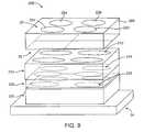
- a thin camera 200may include the multi-surface imaging lens array (ILA) 22 , the color filter 25 and the detector array 24 .
- the multi-surface ILAmay include a first optics substrate 205 , which may have lenses 22 a - 22 d on one surface and the color filter 25 on another surface, a second optics substrate 210 , which may have lens elements thereon, e.g., diffractive optical elements 212 on one side thereof and convex refractive elements 214 on another side thereof, and a final optics substrate 230 having lens elements thereon, e.g., concave refractive elements 232 .
- a spacer substrate 220may be provided between the second optics substrate 210 and final optics substrate 230 . As discussed above with respect to previous embodiments, this spacer substrate 220 may serve as a baffle and may include an opening thereon to allow optical communication between the optical elements. Any desired number of substrates may be provided between the first and final substrates 205 , 230 , with or without spacer substrates therebetween.
- a thin cameramay be realized by using optical elements created on a wafer level, which may be secured using planar surfaces thereof.
- Various mechanisms for providing separation between these optical elementsmay be used. Baffles, which may include the separation mechanisms, may be provided throughout the optical assembly. These separation mechanisms may also seal and protect the optical elements of the optical assembly.
- the final planar surface of the optical systemmay be placed directly on the detector array, i.e., on top of the detector microlens array or the detector cover plate. Diffractive elements and other corrective elements may be used to correct for variations from a desired optical functioning, e.g., focal length variation or aberrations. Lenses having different focal lengths may be provided in an array of cameras, to provide further optical functioning.
- Some embodiments of the present inventionmay use an array of lenses for each camera, e.g., a lens for each color to be imaged by the optical system.
- Other embodiments of the present inventionmay use a single lens for each camera. Using a lens for each color may allow each lens to be optimized for a particular associated wavelength range, may be thinner and may allow the color filter to be placed within the optical system, i.e., after a top surface and before the detector array.
- using the plurality of lenses for each cameramay increase end signal processing to combine resultant images.
- Using a single lensmay fit a more conventional approach, reducing post processing, but cannot be made as thin and may require the color filter to remain in the detector array.
- FIG. 10illustrates a partial plan view of a plurality of thin cameras in accordance with any of the above embodiments formed in parallel.
- all or components of a plurality of thin cameras 500here each including a four lens ILA, may be formed on a wafer 400 .
- One or more of the components of the thin cameras 500may be secured together simultaneously and then singulated, e.g., along lanes 450 and 452 , to form the individual thin cameras 500 .
- the substratesmay be secured on planar surfaces thereof, and may be secured by providing adhesive materials, e.g., epoxy or solder, or may fuse adjoining substrates.
- adhesive materialse.g., epoxy or solder
- kinematic featuresmay be formed lithographically to aid in mating and aligning substrates.
- the creation of passive optical elementsmay be performed lithographically or a master may be made and passive optical elements replicated from this master, either of which will be referred to herein as “lithographs.” Further, a replicated lithograph may be transferred into a substrate, as disclosed, for example, in U.S. Pat. No. 6,027,595, which is incorporated by reference herein.
- the method and material used to make these passive optical elementsmay be determined by the design of the passive optical elements. For example, if a refractive optical element having a large sag is required, replication may be advantageous, as direct lithographic techniques may require a lot of time to create such a lens, since an etch time is directly proportional to the sag.
- plastic materialse.g., polymers. These plastic materials may typically be cheaper and lighter than glass, but may have a higher coefficient of thermal expansion and may have a higher dispersion than glass.
- replicated elementsare made of a polymer and lithographic elements are made of glass. These materials have different coefficients of thermal expansion, different indices of refraction, and different chromatic dispersion characteristics.
- a higher MTFmay be realized compared to using one material alone.
- a systemmay be created using direct lithography for some optical elements and replication for other optical elements.
- At least two of the first substrate, the second substrate, the final substrate and the detector arraymay be created and secured on a wafer level, i.e., a plurality of these elements may be created and secured together, and then singulated to form the stack shown, for example, in FIG. 2 , 7 C, 8 B or 9 .
- Such wafer level creationmay be realized in accordance with the teachings of U.S. Pat. Nos. 6,451,150 and 6,483,627, which are incorporated by reference herein in their entirety. Further, all of the optical elements may be created on a wafer level, even if only secured on a die level. As shown in FIGS.
- substrates having the passive optical elements thereonmay be coextensive with the detector substrate, or the substrate having the detector array may extend beyond the passive optical elements in at least one direction, as shown in FIG. 9 .
- only the final substratemay be coextensive with the detector array.
- Components of the cameras 500may be secured and singulated, and then secured to other components which have also been previously secured and singulated with other components.
- an array of these camerasmay be provided by the different cameras.
- a two by two array of cameras 500one having a standard lens configuration, another having a wide angle lens, another having a telephoto lens, and another having a macro lens, may be formed.
- the largest air gapis typically placed between the last lens surface and the sensor. This is often done because it is difficult to place a lens element directly on or close to the sensor plane. As noted above, with a wafer scale camera, this constraint is removed.
- Optical surfacescan be easily located near the sensor plane as described above. Placing a field flattener near the sensor plane may allow the bulk of the imaging optics, e.g., elements 112 , 124 in FIGS. 7A-7C , elements 162 , 164 , 174 in FIG.
- Embodiments of the present inventionhave been disclosed herein and, although specific terms are employed, they are used and are to be interpreted in a generic and descriptive sense only and not for purpose of limitation.
- any appropriate three or more color components for realizing full color imagingmay be employed.
- circular lenseshave been illustrated for the ILA, other shapes allowing higher packing densities for a higher fill factor, such as hexagonal lenses, may be used.
- different apertureshave been described for providing different images in the sub-cameras having the same color, other optical elements that provide a difference may be used.
- the active areas of the pixels themselvesmay be shaped differently for the different sub-cameras. Accordingly, it will be understood by those of ordinary skill in the art that various changes in form and details may be made without departing from the spirit and scope of the present invention as set forth in the following claims.
Landscapes
- Physics & Mathematics (AREA)
- General Physics & Mathematics (AREA)
- Optics & Photonics (AREA)
- Engineering & Computer Science (AREA)
- Multimedia (AREA)
- Signal Processing (AREA)
- Solid State Image Pick-Up Elements (AREA)
Abstract
Description
Y=0.299R+0.58G+0.114B
U=B−Y
V=R−Y (1)
Thus, the YUV components may be determined from the
Claims (27)
Priority Applications (8)
| Application Number | Priority Date | Filing Date | Title |
|---|---|---|---|
| US11/487,580US8049806B2 (en) | 2004-09-27 | 2006-07-17 | Thin camera and associated methods |
| PCT/US2007/016156WO2008011003A2 (en) | 2006-07-17 | 2007-07-17 | Camera system and associated methods |
| JP2009520799AJP5292291B2 (en) | 2006-07-17 | 2007-07-17 | Manufacturing method of camera system |
| CN2007800336275ACN101512768B (en) | 2006-07-17 | 2007-07-17 | Camera system and associated methods |
| KR1020097003164AKR101185881B1 (en) | 2006-07-17 | 2007-07-17 | Camera system and associated methods |
| EP07796897AEP2044629A4 (en) | 2006-07-17 | 2007-07-17 | CAMERA SYSTEM AND RELATED METHODS |
| US12/805,617US8953087B2 (en) | 2004-04-08 | 2010-08-10 | Camera system and associated methods |
| JP2013087770AJP5372280B2 (en) | 2006-07-17 | 2013-04-18 | Camera system |
Applications Claiming Priority (2)
| Application Number | Priority Date | Filing Date | Title |
|---|---|---|---|
| US10/949,807US7773143B2 (en) | 2004-04-08 | 2004-09-27 | Thin color camera having sub-pixel resolution |
| US11/487,580US8049806B2 (en) | 2004-09-27 | 2006-07-17 | Thin camera and associated methods |
Related Parent Applications (1)
| Application Number | Title | Priority Date | Filing Date |
|---|---|---|---|
| US10/949,807Continuation-In-PartUS7773143B2 (en) | 2004-01-26 | 2004-09-27 | Thin color camera having sub-pixel resolution |
Related Child Applications (1)
| Application Number | Title | Priority Date | Filing Date |
|---|---|---|---|
| PCT/US2007/016156Continuation-In-PartWO2008011003A2 (en) | 2004-04-08 | 2007-07-17 | Camera system and associated methods |
Publications (2)
| Publication Number | Publication Date |
|---|---|
| US20070126898A1 US20070126898A1 (en) | 2007-06-07 |
| US8049806B2true US8049806B2 (en) | 2011-11-01 |
Family
ID=38118334
Family Applications (1)
| Application Number | Title | Priority Date | Filing Date |
|---|---|---|---|
| US11/487,580Expired - Fee RelatedUS8049806B2 (en) | 2004-04-08 | 2006-07-17 | Thin camera and associated methods |
Country Status (1)
| Country | Link |
|---|---|
| US (1) | US8049806B2 (en) |
Cited By (20)
| Publication number | Priority date | Publication date | Assignee | Title |
|---|---|---|---|---|
| US20080170140A1 (en)* | 2007-01-11 | 2008-07-17 | Silver Alan G | Video Camera System Using Multiple Image Sensors |
| US20100165134A1 (en)* | 2006-04-17 | 2010-07-01 | Dowski Jr Edward R | Arrayed Imaging Systems And Associated Methods |
| US20100171866A1 (en)* | 2009-01-05 | 2010-07-08 | Applied Quantum Technologies, Inc. | Multiscale Optical System |
| US20100225799A1 (en)* | 2009-03-03 | 2010-09-09 | Olympus Corporation | Image pickup unit, method of manufacturing image pickup unit and electronic apparatus provided with image pickup unit |
| US20110002053A1 (en)* | 2009-07-02 | 2011-01-06 | David Ovrutsky | Wafer level optical elements and applications thereof |
| US20110102661A1 (en)* | 2008-07-04 | 2011-05-05 | Hiroshi Oshitani | Imaging Lens and Manufacturing Method and Imaging Unit Therefor |
| US20110109777A1 (en)* | 2005-10-13 | 2011-05-12 | Rjs Technology, Inc. | System and method for a high performance color filter mosaic array |
| US20110211106A1 (en)* | 2010-01-04 | 2011-09-01 | Duke University | Monocentric Lens-based Multi-scale Optical Systems and Methods of Use |
| US20120257292A1 (en)* | 2011-04-08 | 2012-10-11 | Himax Technologies Limited | Wafer Level Lens Module and Method for Manufacturing the Wafer Level Lens Module |
| US8388793B1 (en)* | 2011-08-29 | 2013-03-05 | Visera Technologies Company Limited | Method for fabricating camera module |
| CN103579268A (en)* | 2012-08-09 | 2014-02-12 | 全视科技有限公司 | Lens array for partitioned image sensor having color filters |
| US8817394B2 (en)* | 2013-01-17 | 2014-08-26 | Himax Technologies Limited | Lens module and manufacturing method thereof |
| US20140339664A1 (en)* | 2011-12-21 | 2014-11-20 | Heptagon Micro Optics Pte. Ltd | Optical Devices and Opto-electronic Modules and Methods for Manufacturing The Same |
| US8922913B2 (en) | 2013-05-08 | 2014-12-30 | Omnivision Technologies, Inc. | Five-aspheric-surface wafer-level lens systems having wide viewing angle |
| US20160057361A1 (en)* | 2010-10-24 | 2016-02-25 | Linx Computational Imaging Ltd. | Geometrically Distorted Luminance In A Multi-Lens Camera |
| CN105445825A (en)* | 2014-09-04 | 2016-03-30 | 全视技术有限公司 | Wafer level method of making aperture lens and related aperture lens system |
| US9432591B2 (en) | 2009-01-05 | 2016-08-30 | Duke University | Multiscale optical system having dynamic camera settings |
| US9494771B2 (en) | 2009-01-05 | 2016-11-15 | Duke University | Quasi-monocentric-lens-based multi-scale optical system |
| US9635253B2 (en) | 2009-01-05 | 2017-04-25 | Duke University | Multiscale telescopic imaging system |
| US10725280B2 (en) | 2009-01-05 | 2020-07-28 | Duke University | Multiscale telescopic imaging system |
Families Citing this family (98)
| Publication number | Priority date | Publication date | Assignee | Title |
|---|---|---|---|---|
| US7224856B2 (en)* | 2001-10-23 | 2007-05-29 | Digital Optics Corporation | Wafer based optical chassis and associated methods |
| US7961989B2 (en)* | 2001-10-23 | 2011-06-14 | Tessera North America, Inc. | Optical chassis, camera having an optical chassis, and associated methods |
| JP4188394B2 (en)* | 2005-09-20 | 2008-11-26 | フジノン株式会社 | Surveillance camera device and surveillance camera system |
| US20070236591A1 (en)* | 2006-04-11 | 2007-10-11 | Tam Samuel W | Method for mounting protective covers over image capture devices and devices manufactured thereby |
| KR100832073B1 (en)* | 2006-11-15 | 2008-05-27 | 삼성전기주식회사 | Contactless Optical Sensor Module |
| US8456560B2 (en)* | 2007-01-26 | 2013-06-04 | Digitaloptics Corporation | Wafer level camera module and method of manufacture |
| CA2685080A1 (en) | 2007-04-24 | 2008-11-06 | Flextronics Ap Llc | Small form factor modules using wafer level optics with bottom cavity and flip-chip assembly |
| US8099190B2 (en)* | 2007-06-22 | 2012-01-17 | Asm International N.V. | Apparatus and method for transferring two or more wafers whereby the positions of the wafers can be measured |
| JP2009010261A (en)* | 2007-06-29 | 2009-01-15 | Fujikura Ltd | Semiconductor package and manufacturing method thereof |
| JPWO2009004965A1 (en)* | 2007-07-04 | 2011-02-03 | コニカミノルタオプト株式会社 | Imaging lens, imaging device, and portable terminal |
| US20090032925A1 (en)* | 2007-07-31 | 2009-02-05 | England Luke G | Packaging with a connection structure |
| EP2223173B1 (en)* | 2007-12-19 | 2013-09-04 | Heptagon Micro Optics Pte. Ltd. | Camera device and manufacturing methods therefor |
| TWI505703B (en)* | 2007-12-19 | 2015-10-21 | Heptagon Micro Optics Pte Ltd | Optical module, wafer level package and manufacturing method thereof |
| WO2009087974A1 (en)* | 2008-01-11 | 2009-07-16 | Panasonic Corporation | Binocular camera module |
| US8389920B2 (en)* | 2008-03-13 | 2013-03-05 | Aptina Imaging Corporation | Method and apparatus for breaking surface tension during a recessed color filter array process |
| DK3876510T3 (en) | 2008-05-20 | 2024-11-11 | Adeia Imaging Llc | CAPTURE AND PROCESSING OF IMAGES USING MONOLITHIC CAMERA ARRAY WITH HETEROGENEOUS IMAGES |
| US11792538B2 (en) | 2008-05-20 | 2023-10-17 | Adeia Imaging Llc | Capturing and processing of images including occlusions focused on an image sensor by a lens stack array |
| US8866920B2 (en) | 2008-05-20 | 2014-10-21 | Pelican Imaging Corporation | Capturing and processing of images using monolithic camera array with heterogeneous imagers |
| US7920339B2 (en)* | 2008-07-02 | 2011-04-05 | Aptina Imaging Corporation | Method and apparatus providing singlet wafer lens system with field flattener |
| WO2010074743A1 (en) | 2008-12-22 | 2010-07-01 | Tessera North America, Inc. | Focus compensation for thin cameras |
| US9419032B2 (en)* | 2009-08-14 | 2016-08-16 | Nanchang O-Film Optoelectronics Technology Ltd | Wafer level camera module with molded housing and method of manufacturing |
| EP2502115A4 (en) | 2009-11-20 | 2013-11-06 | Pelican Imaging Corp | CAPTURE AND IMAGE PROCESSING USING A MONOLITHIC CAMERAS NETWORK EQUIPPED WITH HETEROGENEOUS IMAGERS |
| CN102118551A (en)* | 2009-12-31 | 2011-07-06 | 鸿富锦精密工业(深圳)有限公司 | Imaging device |
| CN102131044B (en)* | 2010-01-20 | 2014-03-26 | 鸿富锦精密工业(深圳)有限公司 | Camera module |
| US8928793B2 (en) | 2010-05-12 | 2015-01-06 | Pelican Imaging Corporation | Imager array interfaces |
| US20120147228A1 (en)* | 2010-12-14 | 2012-06-14 | Duparre Jacques | Imaging systems with optical crosstalk suppression structures |
| US8878950B2 (en) | 2010-12-14 | 2014-11-04 | Pelican Imaging Corporation | Systems and methods for synthesizing high resolution images using super-resolution processes |
| US20120154945A1 (en)* | 2010-12-16 | 2012-06-21 | William Mark Hiatt | Optical apertures and applications thereof |
| EP2708019B1 (en) | 2011-05-11 | 2019-10-16 | FotoNation Limited | Systems and methods for transmitting and receiving array camera image data |
| US20130265459A1 (en) | 2011-06-28 | 2013-10-10 | Pelican Imaging Corporation | Optical arrangements for use with an array camera |
| KR20140045458A (en) | 2011-06-28 | 2014-04-16 | 펠리칸 이매징 코포레이션 | Optical arrangements for use with an array camera |
| US20130070060A1 (en) | 2011-09-19 | 2013-03-21 | Pelican Imaging Corporation | Systems and methods for determining depth from multiple views of a scene that include aliasing using hypothesized fusion |
| CN104081414B (en) | 2011-09-28 | 2017-08-01 | Fotonation开曼有限公司 | Systems and methods for encoding and decoding light field image files |
| EP2817955B1 (en) | 2012-02-21 | 2018-04-11 | FotoNation Cayman Limited | Systems and methods for the manipulation of captured light field image data |
| US9210392B2 (en) | 2012-05-01 | 2015-12-08 | Pelican Imaging Coporation | Camera modules patterned with pi filter groups |
| US8791403B2 (en)* | 2012-06-01 | 2014-07-29 | Omnivision Technologies, Inc. | Lens array for partitioned image sensor to focus a single image onto N image sensor regions |
| JP2015534734A (en) | 2012-06-28 | 2015-12-03 | ペリカン イメージング コーポレイション | System and method for detecting defective camera arrays, optical arrays, and sensors |
| US20140002674A1 (en) | 2012-06-30 | 2014-01-02 | Pelican Imaging Corporation | Systems and Methods for Manufacturing Camera Modules Using Active Alignment of Lens Stack Arrays and Sensors |
| US9634051B2 (en)* | 2012-07-17 | 2017-04-25 | Heptagon Micro Optics Pte. Ltd. | Optical devices, in particular computational cameras, and methods for manufacturing the same |
| PL4296963T3 (en) | 2012-08-21 | 2025-04-28 | Adeia Imaging Llc | Method for depth detection in images captured using array cameras |
| WO2014032020A2 (en) | 2012-08-23 | 2014-02-27 | Pelican Imaging Corporation | Feature based high resolution motion estimation from low resolution images captured using an array source |
| US9214013B2 (en) | 2012-09-14 | 2015-12-15 | Pelican Imaging Corporation | Systems and methods for correcting user identified artifacts in light field images |
| EP4307659A1 (en) | 2012-09-28 | 2024-01-17 | Adeia Imaging LLC | Generating images from light fields utilizing virtual viewpoints |
| US9595553B2 (en) | 2012-11-02 | 2017-03-14 | Heptagon Micro Optics Pte. Ltd. | Optical modules including focal length adjustment and fabrication of the optical modules |
| WO2014078443A1 (en) | 2012-11-13 | 2014-05-22 | Pelican Imaging Corporation | Systems and methods for array camera focal plane control |
| US9462164B2 (en) | 2013-02-21 | 2016-10-04 | Pelican Imaging Corporation | Systems and methods for generating compressed light field representation data using captured light fields, array geometry, and parallax information |
| US9374512B2 (en) | 2013-02-24 | 2016-06-21 | Pelican Imaging Corporation | Thin form factor computational array cameras and modular array cameras |
| US9774789B2 (en) | 2013-03-08 | 2017-09-26 | Fotonation Cayman Limited | Systems and methods for high dynamic range imaging using array cameras |
| US8866912B2 (en) | 2013-03-10 | 2014-10-21 | Pelican Imaging Corporation | System and methods for calibration of an array camera using a single captured image |
| US9521416B1 (en) | 2013-03-11 | 2016-12-13 | Kip Peli P1 Lp | Systems and methods for image data compression |
| US9106784B2 (en) | 2013-03-13 | 2015-08-11 | Pelican Imaging Corporation | Systems and methods for controlling aliasing in images captured by an array camera for use in super-resolution processing |
| US9888194B2 (en) | 2013-03-13 | 2018-02-06 | Fotonation Cayman Limited | Array camera architecture implementing quantum film image sensors |
| WO2014165244A1 (en) | 2013-03-13 | 2014-10-09 | Pelican Imaging Corporation | Systems and methods for synthesizing images from image data captured by an array camera using restricted depth of field depth maps in which depth estimation precision varies |
| US9124831B2 (en) | 2013-03-13 | 2015-09-01 | Pelican Imaging Corporation | System and methods for calibration of an array camera |
| US9578259B2 (en) | 2013-03-14 | 2017-02-21 | Fotonation Cayman Limited | Systems and methods for reducing motion blur in images or video in ultra low light with array cameras |
| WO2014153098A1 (en) | 2013-03-14 | 2014-09-25 | Pelican Imaging Corporation | Photmetric normalization in array cameras |
| US9497429B2 (en) | 2013-03-15 | 2016-11-15 | Pelican Imaging Corporation | Extended color processing on pelican array cameras |
| US9633442B2 (en) | 2013-03-15 | 2017-04-25 | Fotonation Cayman Limited | Array cameras including an array camera module augmented with a separate camera |
| US9438888B2 (en) | 2013-03-15 | 2016-09-06 | Pelican Imaging Corporation | Systems and methods for stereo imaging with camera arrays |
| US10122993B2 (en) | 2013-03-15 | 2018-11-06 | Fotonation Limited | Autofocus system for a conventional camera that uses depth information from an array camera |
| WO2014150856A1 (en) | 2013-03-15 | 2014-09-25 | Pelican Imaging Corporation | Array camera implementing quantum dot color filters |
| US9445003B1 (en) | 2013-03-15 | 2016-09-13 | Pelican Imaging Corporation | Systems and methods for synthesizing high resolution images using image deconvolution based on motion and depth information |
| TWI490526B (en)* | 2013-07-05 | 2015-07-01 | Pixart Imaging Inc | Optical sensing module and electronical apparatus having the same |
| US9898856B2 (en) | 2013-09-27 | 2018-02-20 | Fotonation Cayman Limited | Systems and methods for depth-assisted perspective distortion correction |
| US9264592B2 (en) | 2013-11-07 | 2016-02-16 | Pelican Imaging Corporation | Array camera modules incorporating independently aligned lens stacks |
| US10119808B2 (en) | 2013-11-18 | 2018-11-06 | Fotonation Limited | Systems and methods for estimating depth from projected texture using camera arrays |
| WO2015081279A1 (en) | 2013-11-26 | 2015-06-04 | Pelican Imaging Corporation | Array camera configurations incorporating multiple constituent array cameras |
| US10089740B2 (en) | 2014-03-07 | 2018-10-02 | Fotonation Limited | System and methods for depth regularization and semiautomatic interactive matting using RGB-D images |
| US20150281601A1 (en)* | 2014-03-25 | 2015-10-01 | INVIS Technologies Corporation | Modular Packaging and Optical System for Multi-Aperture and Multi-Spectral Camera Core |
| US9247117B2 (en) | 2014-04-07 | 2016-01-26 | Pelican Imaging Corporation | Systems and methods for correcting for warpage of a sensor array in an array camera module by introducing warpage into a focal plane of a lens stack array |
| US9300877B2 (en)* | 2014-05-05 | 2016-03-29 | Omnivision Technologies, Inc. | Optical zoom imaging systems and associated methods |
| US9270953B2 (en) | 2014-05-16 | 2016-02-23 | Omnivision Technologies, Inc. | Wafer level camera having movable color filter grouping |
| US9521319B2 (en) | 2014-06-18 | 2016-12-13 | Pelican Imaging Corporation | Array cameras and array camera modules including spectral filters disposed outside of a constituent image sensor |
| US9632384B2 (en)* | 2014-08-01 | 2017-04-25 | Apple Inc. | Electrically activated lens component with interlock feature |
| JP2017531976A (en) | 2014-09-29 | 2017-10-26 | フォトネイション ケイマン リミテッド | System and method for dynamically calibrating an array camera |
| US9942474B2 (en) | 2015-04-17 | 2018-04-10 | Fotonation Cayman Limited | Systems and methods for performing high speed video capture and depth estimation using array cameras |
| US9829698B2 (en) | 2015-08-31 | 2017-11-28 | Panasonic Corporation | Endoscope |
| US20180017741A1 (en)* | 2016-07-15 | 2018-01-18 | Advanced Semiconductor Engineering, Inc. | Semiconductor package device and method of manufacturing the same |
| US10482618B2 (en) | 2017-08-21 | 2019-11-19 | Fotonation Limited | Systems and methods for hybrid depth regularization |
| US10935771B2 (en) | 2017-12-21 | 2021-03-02 | Anteryon International B.V. | Lens system |
| CN111727396B (en)* | 2017-12-21 | 2022-05-13 | 安特尔耀恩国际有限公司 | Lens system |
| US11270110B2 (en) | 2019-09-17 | 2022-03-08 | Boston Polarimetrics, Inc. | Systems and methods for surface modeling using polarization cues |
| WO2021071992A1 (en) | 2019-10-07 | 2021-04-15 | Boston Polarimetrics, Inc. | Systems and methods for augmentation of sensor systems and imaging systems with polarization |
| DE112020005932T5 (en) | 2019-11-30 | 2023-01-05 | Boston Polarimetrics, Inc. | SYSTEMS AND METHODS FOR SEGMENTATION OF TRANSPARENT OBJECTS USING POLARIZATION CHARACTERISTICS |
| EP4081933A4 (en) | 2020-01-29 | 2024-03-20 | Intrinsic Innovation LLC | Systems and methods for characterizing object pose detection and measurement systems |
| US11797863B2 (en) | 2020-01-30 | 2023-10-24 | Intrinsic Innovation Llc | Systems and methods for synthesizing data for training statistical models on different imaging modalities including polarized images |
| US11953700B2 (en) | 2020-05-27 | 2024-04-09 | Intrinsic Innovation Llc | Multi-aperture polarization optical systems using beam splitters |
| US12020455B2 (en) | 2021-03-10 | 2024-06-25 | Intrinsic Innovation Llc | Systems and methods for high dynamic range image reconstruction |
| US12069227B2 (en) | 2021-03-10 | 2024-08-20 | Intrinsic Innovation Llc | Multi-modal and multi-spectral stereo camera arrays |
| US11954886B2 (en) | 2021-04-15 | 2024-04-09 | Intrinsic Innovation Llc | Systems and methods for six-degree of freedom pose estimation of deformable objects |
| US11290658B1 (en) | 2021-04-15 | 2022-03-29 | Boston Polarimetrics, Inc. | Systems and methods for camera exposure control |
| US12067746B2 (en) | 2021-05-07 | 2024-08-20 | Intrinsic Innovation Llc | Systems and methods for using computer vision to pick up small objects |
| US12175741B2 (en) | 2021-06-22 | 2024-12-24 | Intrinsic Innovation Llc | Systems and methods for a vision guided end effector |
| US12340538B2 (en) | 2021-06-25 | 2025-06-24 | Intrinsic Innovation Llc | Systems and methods for generating and using visual datasets for training computer vision models |
| US12172310B2 (en) | 2021-06-29 | 2024-12-24 | Intrinsic Innovation Llc | Systems and methods for picking objects using 3-D geometry and segmentation |
| US11689813B2 (en) | 2021-07-01 | 2023-06-27 | Intrinsic Innovation Llc | Systems and methods for high dynamic range imaging using crossed polarizers |
| US12293535B2 (en) | 2021-08-03 | 2025-05-06 | Intrinsic Innovation Llc | Systems and methods for training pose estimators in computer vision |
| US20230064097A1 (en)* | 2021-08-26 | 2023-03-02 | Meta Platforms Technologies, Llc | Diffractive optical element (doe) on an imaging sensor to reduce and minimize flare |
Citations (55)
| Publication number | Priority date | Publication date | Assignee | Title |
|---|---|---|---|---|
| US4479143A (en) | 1980-12-16 | 1984-10-23 | Sharp Kabushiki Kaisha | Color imaging array and color imaging device |
| US4804249A (en) | 1986-12-24 | 1989-02-14 | Honeywell Inc. | Optical filter for incoherent imaging systems |
| US5274456A (en) | 1987-12-28 | 1993-12-28 | Hitachi, Ltd. | Semiconductor device and video camera unit using it and their manufacturing method |
| JPH06269010A (en) | 1993-03-13 | 1994-09-22 | Victor Co Of Japan Ltd | Color separation optical system, image pickup method and image pickup device |
| US5355222A (en) | 1992-05-15 | 1994-10-11 | Precision Tracking Fm, Inc. | Optical receiver for area location system |
| US5451766A (en) | 1993-07-12 | 1995-09-19 | U.S. Philips Corporation | Imaging device containing an electrooptic material to adjust the effective focal length of a lens element |
| US5568197A (en) | 1991-04-08 | 1996-10-22 | Canon Kabushiki Kaisha | Camera apparatus having an optical low-pass filter |
| US5671073A (en) | 1995-02-15 | 1997-09-23 | California Institute Of Technology | Holographic storage using shift multiplexing |
| US5748371A (en) | 1995-02-03 | 1998-05-05 | The Regents Of The University Of Colorado | Extended depth of field optical systems |
| US5757423A (en) | 1993-10-22 | 1998-05-26 | Canon Kabushiki Kaisha | Image taking apparatus |
| US5760832A (en) | 1994-12-16 | 1998-06-02 | Minolta Co., Ltd. | Multiple imager with shutter control |
| US6069738A (en) | 1998-05-27 | 2000-05-30 | University Technology Corporation | Apparatus and methods for extending depth of field in image projection systems |
| US6108036A (en) | 1996-03-25 | 2000-08-22 | Sharp Kabushiki Kaisha | Imaging apparatus having a spatial filter and image shifting mechanism controller based on an image mode |
| US6137535A (en) | 1996-11-04 | 2000-10-24 | Eastman Kodak Company | Compact digital camera with segmented fields of view |
| EP1067779A2 (en) | 1999-06-30 | 2001-01-10 | Canon Kabushiki Kaisha | Image pickup apparatus |
| US6285064B1 (en) | 2000-03-28 | 2001-09-04 | Omnivision Technologies, Inc. | Chip scale packaging technique for optical image sensing integrated circuits |
| WO2001099431A2 (en) | 2000-06-16 | 2001-12-27 | University Technology Corporation | Method and apparatus for increasing resolution in digital imaging system by offsetting pixels |
| US20020006687A1 (en) | 2000-05-23 | 2002-01-17 | Lam Ken M. | Integrated IC chip package for electronic image sensor die |
| US6346969B1 (en) | 1996-12-30 | 2002-02-12 | Hyundai Electronics Industries Co., Ltd. | Color filter array and its color interpolation apparatus |
| US6366319B1 (en) | 1997-07-03 | 2002-04-02 | Photronics Corp. | Subtractive color processing system for digital imaging |
| JP2002135796A (en) | 2000-10-25 | 2002-05-10 | Canon Inc | Imaging device |
| EP1215729A2 (en) | 2000-12-18 | 2002-06-19 | Canon Kabushiki Kaisha | Image pickup apparatus |
| US6414296B1 (en) | 2000-09-21 | 2002-07-02 | Imation Corp. | Multiple pixel reading of holographic data including a position error calculation |
| US6417950B1 (en) | 2000-08-28 | 2002-07-09 | University Technology Corporation | Three-color imaging on each pixel for increased resolution |
| US20020089596A1 (en) | 2000-12-28 | 2002-07-11 | Yasuo Suda | Image sensing apparatus |
| US20020122124A1 (en) | 2000-10-25 | 2002-09-05 | Yasuo Suda | Image sensing apparatus and its control method, control program, and storage medium |
| EP1244151A2 (en) | 2001-03-21 | 2002-09-25 | Canon Kabushiki Kaisha | Semiconductor device and its manufacture method |
| WO2002077695A1 (en) | 2001-03-21 | 2002-10-03 | The Regents Of The University Of Colorado | High-speed confocal microscope |
| US20020163582A1 (en) | 2001-05-04 | 2002-11-07 | Gruber Michael A. | Self-calibrating, digital, large format camera with single or mulitiple detector arrays and single or multiple optical systems |
| US20020176148A1 (en) | 2000-03-03 | 2002-11-28 | Ichiro Onuki | Optical apparatus |
| US20020181123A1 (en) | 2001-06-04 | 2002-12-05 | Xiaofeng Han | Astigmatism correcting optical coupler |
| US20020181126A1 (en) | 1998-06-30 | 2002-12-05 | Kimihiko Nishioka | Variable optical-property element |
| WO2003024090A1 (en) | 2001-09-07 | 2003-03-20 | Koninklijke Philips Electronics N.V. | Image device having camera and image perspective correction and possibly rotation and staggering correction |
| US6611289B1 (en) | 1999-01-15 | 2003-08-26 | Yanbin Yu | Digital cameras using multiple sensors with multiple lenses |
| US6632701B2 (en) | 2000-09-25 | 2003-10-14 | Foveon, Inc. | Vertical color filter detector group and array |
| US20040012698A1 (en)* | 2001-03-05 | 2004-01-22 | Yasuo Suda | Image pickup model and image pickup device |
| US20040095502A1 (en) | 2001-02-28 | 2004-05-20 | Reinhard Losehand | Digital camera with a light-sensitive sensor |
| JP2004302095A (en) | 2003-03-31 | 2004-10-28 | Mitsubishi Electric Corp | Imaging device |
| US20050073603A1 (en) | 2003-10-01 | 2005-04-07 | Digital Optics Corporation | Thin camera having sub-pixel resolution |
| US6882364B1 (en) | 1997-12-02 | 2005-04-19 | Fuji Photo Film Co., Ltd | Solid-state imaging apparatus and signal processing method for transforming image signals output from a honeycomb arrangement to high quality video signals |
| WO2005041561A1 (en) | 2003-10-27 | 2005-05-06 | Koninklijke Philips Electronics N.V. | Camera module and manufacturing method for such a camera module |
| US20050104991A1 (en) | 1999-09-03 | 2005-05-19 | Sony Corporation | Imaging element, imaging device, camera module and camera system |
| US20050128335A1 (en) | 2003-12-11 | 2005-06-16 | Timo Kolehmainen | Imaging device |
| US20050242410A1 (en) | 2002-07-18 | 2005-11-03 | Koninklijke Philips Electronics N.V. | Camera module, holder for use in a camera module, camera system and method of manufacturing a camera module |
| US20050248680A1 (en) | 2004-05-04 | 2005-11-10 | Tessera, Inc. | Compact lens turret assembly |
| US20050258350A1 (en) | 2002-09-09 | 2005-11-24 | Koninklijke Philips Electronics, N.V. | Optoelectronic semiconductor device and method of manufacturing such a device |
| US7003177B1 (en) | 1999-03-30 | 2006-02-21 | Ramot At Tel-Aviv University Ltd. | Method and system for super resolution |
| US20060044450A1 (en)* | 2002-09-17 | 2006-03-02 | Koninklijke Philips Electronics, N.C. | Camera device, method of manufacturing a camera device, wafer scale package |
| US7009652B1 (en) | 1999-08-20 | 2006-03-07 | Minolta Co. Ltd | Image input apparatus |
| US7034866B1 (en) | 2000-11-22 | 2006-04-25 | Koninklijke Philips Electronics N.V. | Combined display-camera for an image processing system |
| US7199348B2 (en)* | 2004-08-25 | 2007-04-03 | Newport Imaging Corporation | Apparatus for multiple camera devices and method of operating same |
| US7499093B2 (en)* | 1998-12-24 | 2009-03-03 | Aptina Imaging Corporation | Contoured surface cover plate for image sensor array |
| US7511749B2 (en)* | 2003-12-18 | 2009-03-31 | Aptina Imaging Corporation | Color image sensor having imaging element array forming images on respective regions of sensor elements |
| US7564019B2 (en)* | 2005-08-25 | 2009-07-21 | Richard Ian Olsen | Large dynamic range cameras |
| US7566855B2 (en)* | 2005-08-25 | 2009-07-28 | Richard Ian Olsen | Digital camera with integrated infrared (IR) response |
Family Cites Families (1)
| Publication number | Priority date | Publication date | Assignee | Title |
|---|---|---|---|---|
| JPS6274063U (en)* | 1985-10-30 | 1987-05-12 |
- 2006
- 2006-07-17USUS11/487,580patent/US8049806B2/ennot_activeExpired - Fee Related
Patent Citations (60)
| Publication number | Priority date | Publication date | Assignee | Title |
|---|---|---|---|---|
| US4479143A (en) | 1980-12-16 | 1984-10-23 | Sharp Kabushiki Kaisha | Color imaging array and color imaging device |
| US4804249A (en) | 1986-12-24 | 1989-02-14 | Honeywell Inc. | Optical filter for incoherent imaging systems |
| US5274456A (en) | 1987-12-28 | 1993-12-28 | Hitachi, Ltd. | Semiconductor device and video camera unit using it and their manufacturing method |
| US5568197A (en) | 1991-04-08 | 1996-10-22 | Canon Kabushiki Kaisha | Camera apparatus having an optical low-pass filter |
| US5355222A (en) | 1992-05-15 | 1994-10-11 | Precision Tracking Fm, Inc. | Optical receiver for area location system |
| JPH06269010A (en) | 1993-03-13 | 1994-09-22 | Victor Co Of Japan Ltd | Color separation optical system, image pickup method and image pickup device |
| US5451766A (en) | 1993-07-12 | 1995-09-19 | U.S. Philips Corporation | Imaging device containing an electrooptic material to adjust the effective focal length of a lens element |
| US5757423A (en) | 1993-10-22 | 1998-05-26 | Canon Kabushiki Kaisha | Image taking apparatus |
| US5760832A (en) | 1994-12-16 | 1998-06-02 | Minolta Co., Ltd. | Multiple imager with shutter control |
| US5748371A (en) | 1995-02-03 | 1998-05-05 | The Regents Of The University Of Colorado | Extended depth of field optical systems |
| US5671073A (en) | 1995-02-15 | 1997-09-23 | California Institute Of Technology | Holographic storage using shift multiplexing |
| US6108036A (en) | 1996-03-25 | 2000-08-22 | Sharp Kabushiki Kaisha | Imaging apparatus having a spatial filter and image shifting mechanism controller based on an image mode |
| US6137535A (en) | 1996-11-04 | 2000-10-24 | Eastman Kodak Company | Compact digital camera with segmented fields of view |
| US6346969B1 (en) | 1996-12-30 | 2002-02-12 | Hyundai Electronics Industries Co., Ltd. | Color filter array and its color interpolation apparatus |
| US6366319B1 (en) | 1997-07-03 | 2002-04-02 | Photronics Corp. | Subtractive color processing system for digital imaging |
| US6882364B1 (en) | 1997-12-02 | 2005-04-19 | Fuji Photo Film Co., Ltd | Solid-state imaging apparatus and signal processing method for transforming image signals output from a honeycomb arrangement to high quality video signals |
| US6069738A (en) | 1998-05-27 | 2000-05-30 | University Technology Corporation | Apparatus and methods for extending depth of field in image projection systems |
| US20020181126A1 (en) | 1998-06-30 | 2002-12-05 | Kimihiko Nishioka | Variable optical-property element |
| US7499093B2 (en)* | 1998-12-24 | 2009-03-03 | Aptina Imaging Corporation | Contoured surface cover plate for image sensor array |
| US6611289B1 (en) | 1999-01-15 | 2003-08-26 | Yanbin Yu | Digital cameras using multiple sensors with multiple lenses |
| US7003177B1 (en) | 1999-03-30 | 2006-02-21 | Ramot At Tel-Aviv University Ltd. | Method and system for super resolution |
| US6859229B1 (en) | 1999-06-30 | 2005-02-22 | Canon Kabushiki Kaisha | Image pickup apparatus |
| EP1067779A2 (en) | 1999-06-30 | 2001-01-10 | Canon Kabushiki Kaisha | Image pickup apparatus |
| US7009652B1 (en) | 1999-08-20 | 2006-03-07 | Minolta Co. Ltd | Image input apparatus |
| US20050104991A1 (en) | 1999-09-03 | 2005-05-19 | Sony Corporation | Imaging element, imaging device, camera module and camera system |
| US20020176148A1 (en) | 2000-03-03 | 2002-11-28 | Ichiro Onuki | Optical apparatus |
| US6285064B1 (en) | 2000-03-28 | 2001-09-04 | Omnivision Technologies, Inc. | Chip scale packaging technique for optical image sensing integrated circuits |
| US20020006687A1 (en) | 2000-05-23 | 2002-01-17 | Lam Ken M. | Integrated IC chip package for electronic image sensor die |
| US6541284B2 (en) | 2000-05-23 | 2003-04-01 | Atmel Corporation | Integrated IC chip package for electronic image sensor die |
| WO2001099431A2 (en) | 2000-06-16 | 2001-12-27 | University Technology Corporation | Method and apparatus for increasing resolution in digital imaging system by offsetting pixels |
| US6417950B1 (en) | 2000-08-28 | 2002-07-09 | University Technology Corporation | Three-color imaging on each pixel for increased resolution |
| US6414296B1 (en) | 2000-09-21 | 2002-07-02 | Imation Corp. | Multiple pixel reading of holographic data including a position error calculation |
| US6632701B2 (en) | 2000-09-25 | 2003-10-14 | Foveon, Inc. | Vertical color filter detector group and array |
| US20020122124A1 (en) | 2000-10-25 | 2002-09-05 | Yasuo Suda | Image sensing apparatus and its control method, control program, and storage medium |
| JP2002135796A (en) | 2000-10-25 | 2002-05-10 | Canon Inc | Imaging device |
| US7034866B1 (en) | 2000-11-22 | 2006-04-25 | Koninklijke Philips Electronics N.V. | Combined display-camera for an image processing system |
| EP1215729A2 (en) | 2000-12-18 | 2002-06-19 | Canon Kabushiki Kaisha | Image pickup apparatus |
| US20020089596A1 (en) | 2000-12-28 | 2002-07-11 | Yasuo Suda | Image sensing apparatus |
| US20040095502A1 (en) | 2001-02-28 | 2004-05-20 | Reinhard Losehand | Digital camera with a light-sensitive sensor |
| US20040012698A1 (en)* | 2001-03-05 | 2004-01-22 | Yasuo Suda | Image pickup model and image pickup device |
| US20020163054A1 (en) | 2001-03-21 | 2002-11-07 | Yasuo Suda | Semiconductor device and its manufacture method |
| WO2002077695A1 (en) | 2001-03-21 | 2002-10-03 | The Regents Of The University Of Colorado | High-speed confocal microscope |
| EP1244151A2 (en) | 2001-03-21 | 2002-09-25 | Canon Kabushiki Kaisha | Semiconductor device and its manufacture method |
| US6635941B2 (en)* | 2001-03-21 | 2003-10-21 | Canon Kabushiki Kaisha | Structure of semiconductor device with improved reliability |
| US20020163582A1 (en) | 2001-05-04 | 2002-11-07 | Gruber Michael A. | Self-calibrating, digital, large format camera with single or mulitiple detector arrays and single or multiple optical systems |
| US20020181123A1 (en) | 2001-06-04 | 2002-12-05 | Xiaofeng Han | Astigmatism correcting optical coupler |
| WO2003024090A1 (en) | 2001-09-07 | 2003-03-20 | Koninklijke Philips Electronics N.V. | Image device having camera and image perspective correction and possibly rotation and staggering correction |
| US20050242410A1 (en) | 2002-07-18 | 2005-11-03 | Koninklijke Philips Electronics N.V. | Camera module, holder for use in a camera module, camera system and method of manufacturing a camera module |
| US20050258350A1 (en) | 2002-09-09 | 2005-11-24 | Koninklijke Philips Electronics, N.V. | Optoelectronic semiconductor device and method of manufacturing such a device |
| US20060044450A1 (en)* | 2002-09-17 | 2006-03-02 | Koninklijke Philips Electronics, N.C. | Camera device, method of manufacturing a camera device, wafer scale package |
| JP2004302095A (en) | 2003-03-31 | 2004-10-28 | Mitsubishi Electric Corp | Imaging device |
| US20050073603A1 (en) | 2003-10-01 | 2005-04-07 | Digital Optics Corporation | Thin camera having sub-pixel resolution |
| WO2005041561A1 (en) | 2003-10-27 | 2005-05-06 | Koninklijke Philips Electronics N.V. | Camera module and manufacturing method for such a camera module |
| US20050128335A1 (en) | 2003-12-11 | 2005-06-16 | Timo Kolehmainen | Imaging device |
| US7453510B2 (en)* | 2003-12-11 | 2008-11-18 | Nokia Corporation | Imaging device |
| US7511749B2 (en)* | 2003-12-18 | 2009-03-31 | Aptina Imaging Corporation | Color image sensor having imaging element array forming images on respective regions of sensor elements |
| US20050248680A1 (en) | 2004-05-04 | 2005-11-10 | Tessera, Inc. | Compact lens turret assembly |
| US7199348B2 (en)* | 2004-08-25 | 2007-04-03 | Newport Imaging Corporation | Apparatus for multiple camera devices and method of operating same |
| US7564019B2 (en)* | 2005-08-25 | 2009-07-21 | Richard Ian Olsen | Large dynamic range cameras |
| US7566855B2 (en)* | 2005-08-25 | 2009-07-28 | Richard Ian Olsen | Digital camera with integrated infrared (IR) response |
Non-Patent Citations (11)
| Title |
|---|
| Dowski, Jr., et al., [I] "Aberration Invariant Optical/Digital Incoherent Systems," Imaging Systems Laboratory, Dept. of Electrical Engineering, U.Colorado, Boulder, CO, Optical Review, 3(6A):429-432, (1996). |
| Dowski, Jr., et al., [II] "Aberration Invariant Optical/Digital Incoherent Optical Systems", Imaging Systems Laboratory, Dept. of Electrical Engineering, U.Colorado, Boulder, CO, (3 pages) (1996). |
| Dowski, Jr., et al., [III] "Wavefront Coding: A Modern Method of Achieving High Performance and/or Low Cost Imaging Systems" (9 pages), SPIE, (1999). |
| European Search Report in EP 11153126.5-1234, dated Mar. 24, 2011 (Feldman, et al.). |
| Korean Office action in KR 10-2006-7017082, dated May 17, 2011 (Feldman, et al.). |
| Kubala, et al. "Reducing Complexity in Computational Imaging System", Optical Society of America, © 2003. |
| Machine Translation of JP2004-302095 published Oct. 28, 2004.* |
| Mait, et al. Evolutionary Paths in Imaging and Recent Trends, Optics Express, 11(18):2093-2101 (Sep. 8, 2003). |
| Potuluri, et al. "High Depth of Field Microscopic Imaging Using an Inteferometric Camera", Optics Express, 8(11):624-630 (May 21, 2001). |
| Tanida, et al. Thin Observation Module by Bound Optics (TOMBO): Concept and Experimental Verification, Applied Optics, 40(11):1806-1813 (Apr. 10, 2001). |
| Tanida, et al., "Color Imaging with an Integrated Compound Imaging System", Optics Express, 11(18):2109-2117 (Sep. 8, 2003). |
Cited By (46)
| Publication number | Priority date | Publication date | Assignee | Title |
|---|---|---|---|---|
| US8860857B2 (en)* | 2005-10-13 | 2014-10-14 | Rjs Technology, Inc. | System and method for a high performance color filter mosaic array |
| US20110109777A1 (en)* | 2005-10-13 | 2011-05-12 | Rjs Technology, Inc. | System and method for a high performance color filter mosaic array |
| US20100165134A1 (en)* | 2006-04-17 | 2010-07-01 | Dowski Jr Edward R | Arrayed Imaging Systems And Associated Methods |
| US9418193B2 (en) | 2006-04-17 | 2016-08-16 | Omnivision Technologies, Inc. | Arrayed imaging systems having improved alignment and associated methods |
| US10002215B2 (en) | 2006-04-17 | 2018-06-19 | Omnivision Technologies, Inc. | Arrayed imaging systems having improved alignment and associated methods |
| US8599301B2 (en)* | 2006-04-17 | 2013-12-03 | Omnivision Technologies, Inc. | Arrayed imaging systems having improved alignment and associated methods |
| US8319846B2 (en)* | 2007-01-11 | 2012-11-27 | Raytheon Company | Video camera system using multiple image sensors |
| US20080170140A1 (en)* | 2007-01-11 | 2008-07-17 | Silver Alan G | Video Camera System Using Multiple Image Sensors |
| US20110102661A1 (en)* | 2008-07-04 | 2011-05-05 | Hiroshi Oshitani | Imaging Lens and Manufacturing Method and Imaging Unit Therefor |
| US8542310B2 (en)* | 2008-07-04 | 2013-09-24 | Konica Minolta Opto, Inc. | Imaging lens, manufacturing method and imaging unit therefor |
| US20100171866A1 (en)* | 2009-01-05 | 2010-07-08 | Applied Quantum Technologies, Inc. | Multiscale Optical System |
| US9494771B2 (en) | 2009-01-05 | 2016-11-15 | Duke University | Quasi-monocentric-lens-based multi-scale optical system |
| US8259212B2 (en)* | 2009-01-05 | 2012-09-04 | Applied Quantum Technologies, Inc. | Multiscale optical system |
| US10725280B2 (en) | 2009-01-05 | 2020-07-28 | Duke University | Multiscale telescopic imaging system |
| US9432591B2 (en) | 2009-01-05 | 2016-08-30 | Duke University | Multiscale optical system having dynamic camera settings |
| US9762813B2 (en) | 2009-01-05 | 2017-09-12 | Duke University | Monocentric lens-based multi-scale optical systems and methods of use |
| US9635253B2 (en) | 2009-01-05 | 2017-04-25 | Duke University | Multiscale telescopic imaging system |
| US9256056B2 (en) | 2009-01-05 | 2016-02-09 | Duke University | Monocentric lens-based multi-scale optical systems and methods of use |
| US20100225799A1 (en)* | 2009-03-03 | 2010-09-09 | Olympus Corporation | Image pickup unit, method of manufacturing image pickup unit and electronic apparatus provided with image pickup unit |
| US8422138B2 (en)* | 2009-07-02 | 2013-04-16 | Digitaloptics Corporation East | Wafer level optical elements and applications thereof |
| US9030745B2 (en)* | 2009-07-02 | 2015-05-12 | Nan Chang O-Film Optoelectronics Technology Ltd | Wafer level optical elements and applications thereof |
| US20110002053A1 (en)* | 2009-07-02 | 2011-01-06 | David Ovrutsky | Wafer level optical elements and applications thereof |
| US20110211106A1 (en)* | 2010-01-04 | 2011-09-01 | Duke University | Monocentric Lens-based Multi-scale Optical Systems and Methods of Use |
| US8830377B2 (en) | 2010-01-04 | 2014-09-09 | Duke University | Monocentric lens-based multi-scale optical systems and methods of use |
| US9654696B2 (en) | 2010-10-24 | 2017-05-16 | LinX Computation Imaging Ltd. | Spatially differentiated luminance in a multi-lens camera |
| US9681057B2 (en) | 2010-10-24 | 2017-06-13 | Linx Computational Imaging Ltd. | Exposure timing manipulation in a multi-lens camera |
| US20160057361A1 (en)* | 2010-10-24 | 2016-02-25 | Linx Computational Imaging Ltd. | Geometrically Distorted Luminance In A Multi-Lens Camera |
| US9615030B2 (en) | 2010-10-24 | 2017-04-04 | Linx Computational Imaging Ltd. | Luminance source selection in a multi-lens camera |
| US9413984B2 (en) | 2010-10-24 | 2016-08-09 | Linx Computational Imaging Ltd. | Luminance source selection in a multi-lens camera |
| US9578257B2 (en)* | 2010-10-24 | 2017-02-21 | Linx Computational Imaging Ltd. | Geometrically distorted luminance in a multi-lens camera |
| US20120257292A1 (en)* | 2011-04-08 | 2012-10-11 | Himax Technologies Limited | Wafer Level Lens Module and Method for Manufacturing the Wafer Level Lens Module |
| US8388793B1 (en)* | 2011-08-29 | 2013-03-05 | Visera Technologies Company Limited | Method for fabricating camera module |
| CN107634073A (en)* | 2011-12-21 | 2018-01-26 | 新加坡恒立私人有限公司 | Optical devices and optical-electric module and the method for manufacturing Optical devices and optical-electric module |
| US20170077162A1 (en)* | 2011-12-21 | 2017-03-16 | Heptagon Micro Optics Pte. Ltd. | Optical devices and opto-electronic modules and methods for manufacturing the same |
| CN107403815B (en)* | 2011-12-21 | 2020-11-20 | 新加坡恒立私人有限公司 | Optical devices and optoelectronic modules and methods for manufacturing optical devices and optoelectronic modules |
| US10236314B2 (en)* | 2011-12-21 | 2019-03-19 | Ams Sensors Singapore Pte. Ltd. | Optical devices and opto-electronic modules and methods for manufacturing the same |
| US20140339664A1 (en)* | 2011-12-21 | 2014-11-20 | Heptagon Micro Optics Pte. Ltd | Optical Devices and Opto-electronic Modules and Methods for Manufacturing The Same |
| US9490287B2 (en)* | 2011-12-21 | 2016-11-08 | Heptagon Micro Optics Pte. Ltd. | Optical devices and opto-electronic modules and methods for manufacturing the same |
| CN107403815A (en)* | 2011-12-21 | 2017-11-28 | 新加坡恒立私人有限公司 | Optical devices and optical-electric module and the method for manufacturing Optical devices and optical-electric module |
| CN103579268A (en)* | 2012-08-09 | 2014-02-12 | 全视科技有限公司 | Lens array for partitioned image sensor having color filters |
| US20140327977A1 (en)* | 2013-01-17 | 2014-11-06 | Himax Technologies Limited | Lens module and manufacturing method thereof |
| US8817394B2 (en)* | 2013-01-17 | 2014-08-26 | Himax Technologies Limited | Lens module and manufacturing method thereof |
| US9261629B2 (en)* | 2013-01-17 | 2016-02-16 | Himax Technologies Limited | Lens module and manufacturing method thereof |
| US8922913B2 (en) | 2013-05-08 | 2014-12-30 | Omnivision Technologies, Inc. | Five-aspheric-surface wafer-level lens systems having wide viewing angle |
| CN105445825B (en)* | 2014-09-04 | 2020-10-23 | 豪威科技股份有限公司 | Wafer-level method of manufacturing an apertured lens and associated apertured lens system |
| CN105445825A (en)* | 2014-09-04 | 2016-03-30 | 全视技术有限公司 | Wafer level method of making aperture lens and related aperture lens system |
Also Published As
| Publication number | Publication date |
|---|---|
| US20070126898A1 (en) | 2007-06-07 |
Similar Documents
| Publication | Publication Date | Title |
|---|---|---|
| US8049806B2 (en) | Thin camera and associated methods | |
| US8953087B2 (en) | Camera system and associated methods | |
| KR101185881B1 (en) | Camera system and associated methods | |
| US11978752B2 (en) | Aperture-metasurface and hybrid refractive-metasurface imaging systems | |
| CN105141933B (en) | Thin camera with subpixel resolution | |
| US8259212B2 (en) | Multiscale optical system | |
| US8325266B2 (en) | Method of forming thin camera | |
| US7119319B2 (en) | Solid-state image sensing element and its design support method, and image sensing device | |
| CN1934872B (en) | Thin camera with sub-pixel resolution | |
| US9793308B2 (en) | Imager integrated circuit and stereoscopic image capture device | |
| US20070097249A1 (en) | Camera module | |
| CN105579902A (en) | Camera module and method of manufacturing same | |
| US7157690B2 (en) | Imaging device with triangular photodetector array for use in imaging | |
| US11930256B2 (en) | Imaging device, imaging optical system, and imaging method | |
| US20160234411A1 (en) | Wide-Angle Camera Using Achromatic Doublet Prism Array And Method of Manufacturing The Same | |
| JPH03175403A (en) | Solid-state image pickup device | |
| TWI803719B (en) | Image sensor pixel array with phase detection auto-focus pixels and method for manufacturing the same | |
| JP2008526062A (en) | Image sensor with totally separate color zones | |
| TWI436475B (en) | Optical module and manufacturing method thereof | |
| CN102129106A (en) | Optical module and manufacturing method thereof |
Legal Events
| Date | Code | Title | Description |
|---|---|---|---|
| AS | Assignment | Owner name:DIGITAL OPTICS CORPORATION, NORTH CAROLINA Free format text:ASSIGNMENT OF ASSIGNORS INTEREST;ASSIGNORS:FELDMAN, MICHAEL R.;MORRIS, JAMES E.;TEKOLSTE, ROBERT;REEL/FRAME:018504/0727 Effective date:20060907 | |
| AS | Assignment | Owner name:TESSERA NORTH AMERICA, INC., NORTH CAROLINA Free format text:CHANGE OF NAME;ASSIGNOR:DIGITAL OPTICS CORPORATION;REEL/FRAME:024697/0727 Effective date:20070330 | |
| STCF | Information on status: patent grant | Free format text:PATENTED CASE | |
| AS | Assignment | Owner name:DIGITALOPTICS CORPORATION EAST, NORTH CAROLINA Free format text:CHANGE OF NAME;ASSIGNOR:TESSERA NORTH AMERICA, INC.;REEL/FRAME:027768/0541 Effective date:20110701 | |
| AS | Assignment | Owner name:FLIR SYSTEMS TRADING BELGIUM BVBA, BELGIUM Free format text:ASSIGNMENT OF ASSIGNORS INTEREST;ASSIGNOR:DIGITALOPTICS CORPORATION EAST;REEL/FRAME:032827/0362 Effective date:20130808 | |
| FEPP | Fee payment procedure | Free format text:PAT HOLDER NO LONGER CLAIMS SMALL ENTITY STATUS, ENTITY STATUS SET TO UNDISCOUNTED (ORIGINAL EVENT CODE: STOL); ENTITY STATUS OF PATENT OWNER: SMALL ENTITY | |
| FEPP | Fee payment procedure | Free format text:PAT HOLDER CLAIMS SMALL ENTITY STATUS, ENTITY STATUS SET TO SMALL (ORIGINAL EVENT CODE: LTOS); ENTITY STATUS OF PATENT OWNER: SMALL ENTITY | |
| REMI | Maintenance fee reminder mailed | ||
| AS | Assignment | Owner name:DIGITALOPTICS CORPORATION EAST, NORTH CAROLINA Free format text:CORRECTIVE ASSIGNMENT TO CORRECT THE PATENT NO. 7817833 PREVIOUSLY RECORDED AT REEL: 027768 FRAME: 0541. ASSIGNOR(S) HEREBY CONFIRMS THE ASSIGNMENT;ASSIGNOR:TESSERA NORTH AMERICA, INC.;REEL/FRAME:036733/0896 Effective date:20110701 | |
| FPAY | Fee payment | Year of fee payment:4 | |
| SULP | Surcharge for late payment | ||
| FEPP | Fee payment procedure | Free format text:MAINTENANCE FEE REMINDER MAILED (ORIGINAL EVENT CODE: REM.); ENTITY STATUS OF PATENT OWNER: SMALL ENTITY | |
| LAPS | Lapse for failure to pay maintenance fees | Free format text:PATENT EXPIRED FOR FAILURE TO PAY MAINTENANCE FEES (ORIGINAL EVENT CODE: EXP.); ENTITY STATUS OF PATENT OWNER: SMALL ENTITY | |
| STCH | Information on status: patent discontinuation | Free format text:PATENT EXPIRED DUE TO NONPAYMENT OF MAINTENANCE FEES UNDER 37 CFR 1.362 | |
| FP | Lapsed due to failure to pay maintenance fee | Effective date:20191101 |