US8049685B2 - Passive matrix thin-film electro-luminescent display - Google Patents
Passive matrix thin-film electro-luminescent displayDownload PDFInfo
- Publication number
- US8049685B2 US8049685B2US11/558,093US55809306AUS8049685B2US 8049685 B2US8049685 B2US 8049685B2US 55809306 AUS55809306 AUS 55809306AUS 8049685 B2US8049685 B2US 8049685B2
- Authority
- US
- United States
- Prior art keywords
- display
- resolution
- signal
- low
- resolution component
- Prior art date
- Legal status (The legal status is an assumption and is not a legal conclusion. Google has not performed a legal analysis and makes no representation as to the accuracy of the status listed.)
- Active, expires
Links
Images


Classifications
- G—PHYSICS
- G09—EDUCATION; CRYPTOGRAPHY; DISPLAY; ADVERTISING; SEALS
- G09G—ARRANGEMENTS OR CIRCUITS FOR CONTROL OF INDICATING DEVICES USING STATIC MEANS TO PRESENT VARIABLE INFORMATION
- G09G3/00—Control arrangements or circuits, of interest only in connection with visual indicators other than cathode-ray tubes
- G09G3/20—Control arrangements or circuits, of interest only in connection with visual indicators other than cathode-ray tubes for presentation of an assembly of a number of characters, e.g. a page, by composing the assembly by combination of individual elements arranged in a matrix no fixed position being assigned to or needed to be assigned to the individual characters or partial characters
- G09G3/22—Control arrangements or circuits, of interest only in connection with visual indicators other than cathode-ray tubes for presentation of an assembly of a number of characters, e.g. a page, by composing the assembly by combination of individual elements arranged in a matrix no fixed position being assigned to or needed to be assigned to the individual characters or partial characters using controlled light sources
- G09G3/30—Control arrangements or circuits, of interest only in connection with visual indicators other than cathode-ray tubes for presentation of an assembly of a number of characters, e.g. a page, by composing the assembly by combination of individual elements arranged in a matrix no fixed position being assigned to or needed to be assigned to the individual characters or partial characters using controlled light sources using electroluminescent panels
- G—PHYSICS
- G09—EDUCATION; CRYPTOGRAPHY; DISPLAY; ADVERTISING; SEALS
- G09G—ARRANGEMENTS OR CIRCUITS FOR CONTROL OF INDICATING DEVICES USING STATIC MEANS TO PRESENT VARIABLE INFORMATION
- G09G2300/00—Aspects of the constitution of display devices
- G09G2300/02—Composition of display devices
- G09G2300/023—Display panel composed of stacked panels
- G—PHYSICS
- G09—EDUCATION; CRYPTOGRAPHY; DISPLAY; ADVERTISING; SEALS
- G09G—ARRANGEMENTS OR CIRCUITS FOR CONTROL OF INDICATING DEVICES USING STATIC MEANS TO PRESENT VARIABLE INFORMATION
- G09G2300/00—Aspects of the constitution of display devices
- G09G2300/06—Passive matrix structure, i.e. with direct application of both column and row voltages to the light emitting or modulating elements, other than LCD or OLED
- G—PHYSICS
- G09—EDUCATION; CRYPTOGRAPHY; DISPLAY; ADVERTISING; SEALS
- G09G—ARRANGEMENTS OR CIRCUITS FOR CONTROL OF INDICATING DEVICES USING STATIC MEANS TO PRESENT VARIABLE INFORMATION
- G09G2310/00—Command of the display device
- G09G2310/02—Addressing, scanning or driving the display screen or processing steps related thereto
- G09G2310/0202—Addressing of scan or signal lines
- G09G2310/0205—Simultaneous scanning of several lines in flat panels
- G09G2310/021—Double addressing, i.e. scanning two or more lines, e.g. lines 2 and 3; 4 and 5, at a time in a first field, followed by scanning two or more lines in another combination, e.g. lines 1 and 2; 3 and 4, in a second field
- G—PHYSICS
- G09—EDUCATION; CRYPTOGRAPHY; DISPLAY; ADVERTISING; SEALS
- G09G—ARRANGEMENTS OR CIRCUITS FOR CONTROL OF INDICATING DEVICES USING STATIC MEANS TO PRESENT VARIABLE INFORMATION
- G09G2330/00—Aspects of power supply; Aspects of display protection and defect management
- G09G2330/02—Details of power systems and of start or stop of display operation
- G09G2330/021—Power management, e.g. power saving
Definitions
- the present inventionrelates to passive matrix thin-film electro-luminescent display systems and specifically a method for driving them to decrease their refresh rate and power consumption.
- Electro-luminescent displaywhich is formed by coating a thin layer of electro-luminescent material between a pair of electrodes. Displays employing this technology produce light as a function of the current between the two electrodes when the electro-luminescent materials are electrically stimulated. Electro-luminescent displays are primarily classified as active-matrix or passive-matrix displays. Active-matrix displays employ a relatively complex, active circuit at each pixel in the display to control the flow of current through the electro-luminescent material layer(s). The formation of this active circuit at each pixel can be expensive and often the performance of these circuits is somewhat limited. Passive-matrix displays are much simpler in their construction. Each pair of electrodes at each pixel is formed by the intersection of a row and a column electrode. As this type of display does not require the costly formation of active circuits at each pixel site, they are much less expensive to construct.
- a prior-art displayis illustrated having electrodes 12 and 16 with an electro-luminescent layer 14 formed between the electrodes 12 and 16 and responsive to a current provided by the electrodes 12 and 16 to produce light.
- the two electrodes 12 and 16are typically patterned in orthogonal directions 8 and 6 over a substrate 10 and driven by external row and column drivers (not shown) connected to the electrodes 12 and 16 .
- passive-matrix displayscan be much less expensive to construct than active-matrix displays, they often suffer from relatively severe operational limitations, for example, resolution and refresh rate limitations, which restrict the commercial application of the passive-matrix displays to small, very low-resolution displays. Because of these limitations, the typical passive-matrix thin-film EL display is less than 2 inches in diagonal and has fewer than 150 lines of light-emitting elements. One of the more severe of these limitations occurs due to the fact that the thin-film EL display is formed from a very thin layer of relatively high-resistance EL material between a pair of metal electrodes.
- the EL pixelhas a very high capacitance and when driving this pixel in a display, enough current must be provided to the pixel to overcome the capacitance before the pixel can emit light.
- the larger the pixel, and the thinner the electro-luminescent materialthe larger the capacitance and the more energy that is required to overcome this capacitance before light is produced. Therefore, large displays employing thin films of electro-luminescent materials will require significant power to overcome the capacitance of the pixels in the display.
- the amount of power that is dissipated by charging and discharging the capacitance of the light-emitting elements in the displayincreases. Further, it is necessary to turn on and off a large number of rows of data at the very high rates that occur when the display has a large number of lines (e.g., significantly more than 100 lines) that have to be refreshed at a rate of 70 Hz. Accordingly, it becomes very expensive to construct drivers that are capable of providing high enough currents to perform the required process of pre-charging each pixel, providing current to light each pixel, and then providing sufficient reverse bias in order to perform this refresh process. Therefore, it is not only necessary to reduce the amount of power that is dissipated in pre-charging and reverse biasing each light-emitting element, but to also reduce the peak current that must be provided by the drivers.
- US Patent Application 2002/0101179filed Dec. 27, 2001 by Kawashima, entitled “Organic Electroluminescence Driving Circuit, Passive Matrix Organic Electroluminescence Display Device, and Organic Electroluminescence Driving Method,” suggests driving the passive-matrix display using two power supplies.
- the first power supplyserves as a “voltage holding” supply.
- the second of these power suppliesis used to provide current to activate the light-emitting elements of the display (i.e., provide current to light each light-emitting element). In such a device, all but the active light-emitting elements are attached to the voltage holding supply.
- This power supplymaintains the charge in the capacitors at or near the threshold of the light-emitting diodes such that the light-emitting elements do not have to be charged or discharged.
- Such displayswill often have leakage current near this threshold, and therefore require power to be dissipated even when the display is intended to be dark, which of course also elevates the black level of the display somewhat as the light-emitting elements will produce a small amount of light in response to this leakage current.
- One of the matrices in each orthogonal pairis then used to provide a signal to the row drivers while the second of the matrices in the same orthogonal pair is used to provide a signal to the column drivers.
- These row and column driver inputsare then updated to display each of the orthogonal pairs of matrices during each image update cycle.
- pre-charging and reverse biasing of the light-emitting elementsare avoided, reducing the overall power required to drive the passive matrix display and decreasing the instantaneous current load that is required from each of the drivers.
- the image processing that is required to create the orthogonal pairs of matricesis significant, especially when such processing must be accomplished in real time and at rates of 30 Hz or higher.
- the driversmust be equipped with significant memory and be capable of driving each row to several drive voltage levels.
- a passive-matrix, thin-film electro-luminescent display systemthat includes a display having a substrate with organic layers and orthogonally-arranged electrodes formed thereon.
- One or more display driversreceives an input image signal for addressing the light-emitting elements of the display; (ii) decomposes the signal into a low-resolution component signal and a high-resolution component signal, wherein the low-resolution component signal contains one half or less of the number of addressable locations as the high-resolution component signal; and (iii) provides a drive signal for driving the display wherein the low-resolution component signal and the high-resolution component signal are independently provided to the display to form a combined image.
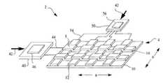
- FIG. 1is a perspective view of a passive-matrix display and controller according to an embodiment of the present invention
- FIG. 2is a perspective view of a single light-emitting element of a passive-matrix display according to an embodiment of the present invention
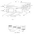
- FIG. 3is a cross section of stacked light-emitting elements of a passive-matrix display formed on opposite sides of a single substrate according to an alternative embodiment of the present invention
- FIG. 4is a cross section of stacked light-emitting elements of a passive-matrix display formed on two substrates according to an alternative embodiment of the present invention
- FIG. 5is a perspective view of stacked light-emitting elements of a passive-matrix display formed on one substrate and sharing an electrode according to an alternative embodiment of the present invention
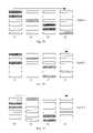
- FIG. 6is an illustration of prior-art temporal control of a passive-matrix display
- FIGS. 7A-7Care an illustration of row-interleaved temporal control of a passive-matrix display according to an embodiment of the present invention.
- FIG. 8is an illustration of row-interleaved temporal control of a passive-matrix display according to an alternative embodiment of the present invention.
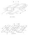
- FIG. 9is an illustration of two-dimensionally interleaved temporal control of a passive-matrix display according to another embodiment of the present invention.
- FIG. 10is an illustration of row-interleaved temporal control of a passive-matrix display according to another alternative embodiment of the present invention.
- FIGS. 11A-11Dare an illustration of frame-interleaved temporal control of a passive-matrix display according to an embodiment of the present invention.
- FIG. 12is a flow diagram illustrating a method of the present invention.
- FIG. 13is a perspective view of a light-emitting element of a prior-art passive-matrix display.
- FIG. 14is a perspective view of a prior-art passive-matrix display.
- a passive-matrix, thin-film electro-luminescent display system 2having improved efficiency, comprising a display 4 consisting of a substrate 10 , a first electrode layer 12 patterned to form lines along a first dimension 6 of the substrate 10 , one or more thin-film electro-luminescent layers 14 formed on the first electrode layer 12 and a second electrode layer 16 formed on the one or more thin-film electro-luminescent layer(s) 14 wherein the second electrode layer 16 is patterned to form lines along a second dimension 8 of the substrate 10 different from the first dimension 6 comprising an electro-luminescent unit 5 .
- Individual light-emitting elements 5are formed at the intersection of the lines of the first and second electrode layers 12 and 16 , respectively; and one or more display drivers 40 , 50 for receiving an input image signal 42 for addressing the light-emitting elements 5 of the display 4 , decomposing the input image signal 42 into a low-resolution component signal and a high-resolution component signal wherein the low-resolution component signal contains one half or less of the number of addressable locations as the high-resolution component signal; and providing a drive signal 44 , 54 for driving the display 4 .
- the low-resolution component signal and the high-resolution component signalare independently provided to the display 4 to form a final image such that the refresh rate of the display 4 may be reduced; thereby; reducing the power used to charge the capacitance of the light-emitting elements 5 .
- the passive-matrix displaymay have greater resolution without requiring an increase in power consumption.
- the first and second electrodes 12 , 16are formed orthogonally over the surface of the display 4 and are often referred to as row and column electrodes. Electrical signals are provided to the first and second electrodes by row driver 46 and column driver 56 . These row and column drivers may be a single integrated circuit or, as shown, separate devices. Additional digital logic or analog circuitry (not shown) may be provided to receive an input image signal 42 and to decompose the signal into a low-resolution component signal and a high-resolution component signal which is provided through the row driver 40 and column driver 50 .
- Such circuitryis known in the art, as are methods for forming electrodes and depositing electro-luminescent materials between the electrodes; for example, by employing OLED, PLED, or inorganic light-emitting materials.
- OLEDorganic light-emitting
- PLEDorganic light-emitting diode
- inorganic light-emitting materialsfor example, by employing OLED, PLED, or inorganic light-emitting materials.
- the formation of electrodes in passive-matrix configurations over a substrateis also known, for example, by employing photolithography to pattern the first electrodes 12 , evaporative or coating techniques to form the electro-luminescent layer 14 , and employing pillars (not shown in FIGS. 1 and 2 ) to pattern the second electrodes 16 .
- the electro-luminescent layer 14may emit a single color or a broadband light such as white, or be patterned to emit different colors at different locations over the substrate 10 .
- Color filtersmay be employed to provide patterned color emission. As described herein, rows and columns are arbitrary designations and may be exchanged in various embodiments of the present invention.
- the present inventionprovides an improved resolution display without increasing the refresh rate or power requirements of the display.
- the apparent resolution of the displaymay stay the same while power usage is reduced.
- the power usageis reduced by requiring fewer charge/discharge cycles of rows or columns or the same number of charge/discharge cycles at a lower refresh frequency, thereby reducing the power required to drive the rows or columns.
- the human visual systemis sensitive to either high spatial resolution component information at a relatively lower temporal frequency or low spatial resolution information at a relatively higher temporal frequency, but not both at the same time, providing the high-spatial resolution component information at a relatively lower temporal frequency and the low spatial resolution information at a relatively higher temporal frequency apparent display resolution is maintained, while reducing the required refresh rate for the high spatial resolution component information, the power requirements are reduced as compared to a prior-art display having a similar resolution.
- This limitationserves to take optimal advantage of the bandwidth of the human visual system (HVS) and can be employed to likewise optimize the performance of a passive-matrix display system.
- a passive-matrix display optimized to take advantage of the spatial frequency response of the HVScan include alternating high- and low-resolution component signals driven to a single display.
- a low-spatial resolution component signalmight be written more often than a high spatial resolution component signal, less often, or at the same frequency.
- a full frame of each signal typemight be temporally interleaved or groups of lines or single lines of each signal type might be temporally interleaved.
- the low spatial resolution component signalwill preferably be written more often than the high spatial resolution component signal.
- the conceptcan be extended to any size display and/or multiple levels of resolution.
- the low-resolution component linesshould be contiguous, generally, since they all receive the same signal. However, they need not be the same lines each time (ignoring top and bottom edge effects).
- the high-resolution component linesmay be chosen arbitrarily. Note that the averaging is only necessary in one dimension, since the same number of columns is employed in the other dimension in either case.
- high- and low-resolution componentit is also possible to write high- and low-resolution component to different levels of a stacked display.
- the colorsmay be treated differently, for example, one may display green high spatial resolution component more frequently than red or blue since both the temporal and spatial resolution of the human visual system tends to be lower for red or blue than for high luminance signals such as green.
- greenLikewise, in an RGBW system, white might get more high-resolution component signals.
- electro-luminescent elements 5may be formed on either side of a substrate 10 by employing an additional first electrode 13 , additional electro-luminescent layer 18 , and additional second electrode 20 on a second side of the substrate 10 .
- the displaymay further comprise a second substrate 19 .
- a first plurality of electro-luminescent elements 5 a in a first stack layer 24are formed on the first substrate 10 and is driven by the low-resolution component signal while a second plurality of electro-luminescent elements 5 b in a second stack layer 26 are formed on the second substrate 19 and is driven by the high-resolution component signal.
- the high- and low-resolution elementsmay be exchanged with respect to the first and second substrates 19 .
- the second substrate 19is located on the patterning pillars 11 ; however, the second substrate 19 is not limited to that location and may be located anywhere above (or below) the first substrate 10 .
- the substrates and electrodes through which light travelsshould preferably be transparent.
- the back substrate and/or electrodemay be opaque or reflective while the others are transparent.
- the location of the reflective or opaque electrodedepends upon whether the device is intended to be a top- or a bottom-emitting device. Note that the first stack layer 24 and the second stack layer 26 are oriented such that one is viewed through an additional substrate 19 as compared to the other.
- additional layers that may serve as an insulatormay be placed over the top of one or both of the first and second stack layers 24 , 26 , to provide electrical insulation and the first and second stack layers 24 , 26 may be arranged such that both substrates 10 , 19 are external to the device and provide a means for creating physical protection of the active areas of the device.
- two electro-luminescent elementsmay be stacked on top of each other and share a common electrode 16 .
- Such structures and means for driving themare discussed in more detail in commonly assigned, co-pending U.S. patent application Ser. No. 11/536,712, filed Sep. 29, 2006 by Cok, which is hereby incorporated in its entirety by reference.
- the displayfurther comprises one or more thin-film electro-luminescent layers 18 which together comprise a second electro-luminescent unit and at least a third electrode layer 20 and wherein the low-resolution component signal is used to drive a first electro-luminescent unit at a first refresh rate and the high-resolution component signal is used to drive a second electro-luminescent unit at a second refresh rate.
- the first plurality of electro-luminescent elementsare shown formed at the same resolution on the first substrate as the second plurality of electro-luminescent elements formed on the second substrate (or on the other side of the same substrate).
- the first plurality of electro-luminescent elementsmay be formed at a relatively lower resolution on the first substrate and the second plurality of electro-luminescent elements are formed at a relatively higher resolution on the second substrate.
- the substratecomprises two sides (as shown in FIG.
- the first plurality of electro-luminescent elements formed on a first side of the substratemay be driven by the low-resolution component signal and the second plurality of electro-luminescent elements formed on the second side of the substrate may be driven by the high-resolution component signal.
- the present inventionmay employ a common refresh rate for both the high- and the low-resolution signals, in some embodiments of the present invention, the refresh rates for the high- and the low-resolution signals may be different. In simpler embodiments, the refresh rates may differ by integral values or by multiples of each other. In particular, the first refresh rate may be at least twice the second refresh rate.
- either the rows or columns of a displaymay be driven at different refresh rates, or both may be driven at different refresh rates.
- multiple light-emitting elements along both dimensions of the displaymay be activated when the low-resolution component signal is provided to the display and multiple light-emitting elements along only one dimension of the display are activated when the high-resolution component signal is provided to the display.
- the low-resolution signalmay drive a plurality of contiguous elements in one or more rows or columns simultaneously with the same signal and the high-resolution signal alternately drives one row or column.
- the low-resolution signalmay be displayed more frequently than the high-resolution signal.
- the low-resolution signal and high-resolution signalmay be interleaved full-frame signals or the low-resolution signal and high-resolution signals are interleaved row or column signals.
- the low-and high-resolution signalsmay be alternately displayed on the electro-luminescent elements.
- the low-resolution signalis displayed on some or all of the rows or columns in the group and the high-resolution signal is alternately and cyclically displayed on one or more of the rows or columns, respectively, in the group.
- the rows or columnsmay be grouped into a plurality of disjoint sets of contiguous rows or columns, respectively, and the low-resolution signal is displayed on some or all of the rows or columns in the group and the high-resolution signal is alternately displayed on one or more of the rows or columns in a different group.
- each columnis labeled with a different time period and each time-labeled column represents an entire display driven at the time period indicated.
- the arrowsindicate a temporal sequence. Only the rows are shown and all of the light-emitting elements in each row are operated simultaneously where indicated by a dotted pattern for a low-resolution component signal and a slash pattern for a high-resolution component signal.
- the orthogonal columns overlapping the rows to form light-emitting elementsare not illustrated (except in FIG. 9 ). As shown in the prior-art illustration of FIG.
- the first rowis controlled with a signal to emit light (in concert with the column control signal, not shown).
- the second rowis operated, at t 2 the third row is operated, and at t 3 the fourth row is operated. All of the light-emitting elements are operated in four time periods comprising a frame refresh cycle, and then the process repeats. The periods are made short enough that an observer does not perceive flicker from the temporally sequential energizing of the rows.
- a six-row display having improved resolutionis operated for three refresh cycles having four periods each, thereby demonstrating improved resolution of the display device using the same time and power as the display of FIG. 6 .
- the first two rowsare operated with a low-resolution component signal.
- the two rowsare energized with the same column signal, allowing them to be operated simultaneously.
- This common, low-resolution component signalmay be the average of the signals for each row, the minimum value of each row the signal for one row or the other or some proportion of one of these quantities.
- a low-resolution component signalis provided.
- a high-resolution component signalis provided to row 3 .
- the high-resolution component signalmay simply be the original row signal.
- a low-resolution component, common signalis provided to rows four and five, and at t 3 a high-resolution component signal is provided to row 6 .
- a second refresh cycle of the same display and illustrated in FIG. 7Bthe first and third rows are operated with a common signal at time t 0 , a high-resolution component signal is supplied to row two at t 1 , the fourth and sixth rows are operated at time t 2 with a common signal, and at t 3 a high-resolution component signal is provided to row 5 .
- a third refresh cycle illustrated in FIG. 7Ca similar procedure is followed, except that the high-resolution component signals are applied to rows one and four, and the low-resolution component signals are supplied to rows two and three and to rows five and six. While it is not necessary that the high-resolution component signals cycle through all of the rows, improved appearance and reduced flickering will result if such cycling is employed.
- the order of the cyclesis not critical.
- the processmay be extended to displays having more rows and low-resolution component signals may also be provided, for example, as shown in FIG. 8 for a single frame cycle, three or more rows may be averaged together for the low-resolution component signal and fewer high-resolution component signals provided relative to the number of low-resolution component signals.
- a two-dimensional subset of the light-emitting elementsmay be driven in common with a low-resolution component signal (as shown at t 0 and t 2 ) and a two-dimensional subset likewise driven with a high-resolution component signal (as shown at t 1 and t 3 ).
- one or the other of the high- and low-resolution component signalsmay include all of the elements in one or more rows; and the other of the high- and low-resolution component signals may include a two-dimensional subset.
- the refresh rate of the high-resolution component signalmay differ from the refresh rate of the low-resolution component.
- rows one and threemay be simultaneously driven at t 0 with a common low-resolution component signal.
- row fourmay be driven with a high-resolution component signal, and at t 2 row two may be driven with a high-resolution component signal.
- a similar schememay be employed for rows five through eight. In this case the high-resolution component signals are driven twice as often as the low-resolution component signals. Note that in this illustration, the display has eight rows and six time periods are used for a frame refresh cycle.
- the low-resolution component signalsare driven twice as often as the low-resolution component signals.
- FIGS. 7-10employ alternate low and high-resolution signals by rows or groups of rows.
- the entire display including all of the light-emitting elementsmay be driven first by the low-resolution signal and then the entire display, including all of the light-emitting elements, may be driven secondly by the high-resolution signal (or vice versa).
- FIG. 11A-Da display having eight rows driven in four time periods comprising a frame refresh cycle is shown.
- the first two rowsare driven with a common, low-resolution signal
- time t 1 rowsthree and four are similarly driven, then rows five and six, followed by rows seven and eight.
- This frame cycleeffectively drives the entire display with a low-resolution component signal in four periods.
- a second frame cycleFIG. 11B
- every other rowis driven with a high-resolution component signal.
- the low-resolution component signalis applied again (illustrated here with different temporal row ordering) and in the fourth cycle ( FIG. 11D ) the rows not driven in the second frame cycle ( FIG. 11B ) are driven with the high-resolution component signal.
- It is also possible to drive the display with relatively more low-resolution component signalsfor example, by driving the display according to the order of frame cycles of FIGS. 11A , 11 C, 11 B, 11 A, 11 C, 11 D and so on.
- it is also possible to drive the display with relatively more high-resolution component signalsfor example by driving the display according to the order of frame cycles of FIGS. 11A , 11 B, 11 D, 11 C, 11 B, 11 D and so on.
- the ordering of the rows presentedmay be varied.
- a passive-matrix displaymay be controlled by receiving an input image signal in operation 100 for addressing the light-emitting elements of the display.
- Operation 105decomposes the input image signal into a low-resolution component signal and a high-resolution component signal, wherein the low-resolution component signal contains one half or less of the number of addressable locations as the high-resolution component signal.
- Operation 110provides a drive signal for driving the display wherein the low-resolution component signal and the high-resolution component signal are independently provided to the display to form a final image.
- the present inventionis employed in a flat-panel OLED device composed of small molecule or polymeric OLEDs as disclosed in but not limited to U.S. Pat. No. 4,769,292, issued Sep. 6, 1988 to Tang et al., and U.S. Pat. No. 5,061,569, issued Oct. 29, 1991 to VanSlyke et al.
- organic light-emitting displayscan be used to fabricate such a device, including passive-matrix OLED displays having either a top- or bottom-emitter architecture.
Landscapes
- Engineering & Computer Science (AREA)
- Physics & Mathematics (AREA)
- Computer Hardware Design (AREA)
- General Physics & Mathematics (AREA)
- Theoretical Computer Science (AREA)
- Electroluminescent Light Sources (AREA)
- Control Of Indicators Other Than Cathode Ray Tubes (AREA)
- Control Of El Displays (AREA)
Abstract
Description
- 2 display system
- 4 display
- 5,5a,5belectro-luminescent element
- 6 first dimension
- 8 second dimension
- 10 substrate
- 11 pillar
- 12 first electrode
- 13 first electrode
- 14 layer of electro-luminescent material
- 16 second electrode
- 18 second layer of electro-luminescent material
- 19 second substrate
- 20 second electrode
- 24 first stack layer
- 26 second stack layer
- 40 driver
- 42 input signal
- 44 drive signal
- 46 circuit
- 50 driver
- 52 input signal
- 54 drive signal
- 56 circuit
- 100 receive signal step
- 105 decompose signal step
- 110 drive display step
Claims (16)
Priority Applications (6)
| Application Number | Priority Date | Filing Date | Title |
|---|---|---|---|
| US11/558,093US8049685B2 (en) | 2006-11-09 | 2006-11-09 | Passive matrix thin-film electro-luminescent display |
| JP2009536237AJP5167267B2 (en) | 2006-11-09 | 2007-10-26 | Passive matrix thin-film electroluminescent display |
| PCT/US2007/022727WO2008063348A2 (en) | 2006-11-09 | 2007-10-26 | Passive matrix thin-film electro-luminescent display |
| KR1020097009411AKR101249459B1 (en) | 2006-11-09 | 2007-10-26 | Passive matrix thin-film electro-luminescent display |
| EP11008346.6AEP2426659B1 (en) | 2006-11-09 | 2007-10-26 | Passive matrix thin-film electro-luminescent display |
| EP07861540AEP2092504A2 (en) | 2006-11-09 | 2007-10-26 | Passive matrix thin-film electro-luminescent display |
Applications Claiming Priority (1)
| Application Number | Priority Date | Filing Date | Title |
|---|---|---|---|
| US11/558,093US8049685B2 (en) | 2006-11-09 | 2006-11-09 | Passive matrix thin-film electro-luminescent display |
Publications (2)
| Publication Number | Publication Date |
|---|---|
| US20080111771A1 US20080111771A1 (en) | 2008-05-15 |
| US8049685B2true US8049685B2 (en) | 2011-11-01 |
Family
ID=39110882
Family Applications (1)
| Application Number | Title | Priority Date | Filing Date |
|---|---|---|---|
| US11/558,093Active2029-10-04US8049685B2 (en) | 2006-11-09 | 2006-11-09 | Passive matrix thin-film electro-luminescent display |
Country Status (5)
| Country | Link |
|---|---|
| US (1) | US8049685B2 (en) |
| EP (2) | EP2092504A2 (en) |
| JP (1) | JP5167267B2 (en) |
| KR (1) | KR101249459B1 (en) |
| WO (1) | WO2008063348A2 (en) |
Cited By (2)
| Publication number | Priority date | Publication date | Assignee | Title |
|---|---|---|---|---|
| US9524666B2 (en) | 2014-12-03 | 2016-12-20 | Revolution Display, Llc | OLED display modules for large-format OLED displays |
| US9779478B1 (en)* | 2016-10-04 | 2017-10-03 | Oculus Vr, Llc | Rendering composite content on a head-mounted display including a high resolution inset |
Families Citing this family (10)
| Publication number | Priority date | Publication date | Assignee | Title |
|---|---|---|---|---|
| US8265166B2 (en)* | 2007-05-14 | 2012-09-11 | Sandisk Il Ltd. | Dual decoder portable media device |
| DE102008024126A1 (en)* | 2008-05-19 | 2009-12-03 | X-Motive Gmbh | Method and driver for driving a passive matrix OLED display |
| US8248358B2 (en)* | 2009-03-27 | 2012-08-21 | Qualcomm Mems Technologies, Inc. | Altering frame rates in a MEMS display by selective line skipping |
| US20130100176A1 (en)* | 2011-10-21 | 2013-04-25 | Qualcomm Mems Technologies, Inc. | Systems and methods for optimizing frame rate and resolution for displays |
| JP2015501944A (en)* | 2011-11-11 | 2015-01-19 | クォルコム・メムズ・テクノロジーズ・インコーポレーテッド | System, device and method for driving a display |
| CN103854596A (en)* | 2012-11-29 | 2014-06-11 | 利亚德光电股份有限公司 | Led display |
| US10417947B2 (en)* | 2015-06-30 | 2019-09-17 | Rockwell Collins, Inc. | Fail-operational emissive display with redundant drive elements |
| US10937924B2 (en) | 2016-10-08 | 2021-03-02 | Goertek. Inc | Display device and electronics apparatus |
| US10824022B2 (en)* | 2017-06-06 | 2020-11-03 | Liqxtal Technology Inc. | Liquid crystal lens and manufacturing method thereof |
| US12424168B2 (en)* | 2021-11-30 | 2025-09-23 | Sharp Display Technology Corporation | Display device |
Citations (62)
| Publication number | Priority date | Publication date | Assignee | Title |
|---|---|---|---|---|
| US4528561A (en)* | 1980-08-11 | 1985-07-09 | Canon Kabushiki Kaisha | Information output device for recording information with varied resolution |
| US4769292A (en) | 1987-03-02 | 1988-09-06 | Eastman Kodak Company | Electroluminescent device with modified thin film luminescent zone |
| US4821208A (en)* | 1986-06-18 | 1989-04-11 | Technology, Inc. | Display processors accommodating the description of color pixels in variable-length codes |
| US5025394A (en)* | 1988-09-09 | 1991-06-18 | New York Institute Of Technology | Method and apparatus for generating animated images |
| US5061569A (en) | 1990-07-26 | 1991-10-29 | Eastman Kodak Company | Electroluminescent device with organic electroluminescent medium |
| US5488674A (en)* | 1992-05-15 | 1996-01-30 | David Sarnoff Research Center, Inc. | Method for fusing images and apparatus therefor |
| US5488687A (en)* | 1992-09-17 | 1996-01-30 | Star Technologies, Inc. | Dual resolution output system for image generators |
| US5612715A (en)* | 1991-07-01 | 1997-03-18 | Seiko Epson Corporation | System and method for dynamically adjusting display resolution of computer generated displays |
| US5642125A (en)* | 1992-06-17 | 1997-06-24 | Xerox Corporation | Two path liquid crystal light valve color display |
| US5644324A (en)* | 1993-03-03 | 1997-07-01 | Maguire, Jr.; Francis J. | Apparatus and method for presenting successive images |
| US5696531A (en)* | 1991-02-05 | 1997-12-09 | Minolta Camera Kabushiki Kaisha | Image display apparatus capable of combining image displayed with high resolution and image displayed with low resolution |
| US5703436A (en)* | 1994-12-13 | 1997-12-30 | The Trustees Of Princeton University | Transparent contacts for organic devices |
| US5726670A (en)* | 1992-07-20 | 1998-03-10 | Olympus Optical Co., Ltd. | Display apparatus to be mounted on the head or face of an individual |
| US5808589A (en)* | 1994-08-24 | 1998-09-15 | Fergason; James L. | Optical system for a head mounted display combining high and low resolution images |
| US6078427A (en)* | 1998-12-01 | 2000-06-20 | Kaiser Electro-Optics, Inc. | Smooth transition device for area of interest head-mounted display |
| US6222675B1 (en)* | 1998-12-01 | 2001-04-24 | Kaiser Electro-Optics, Inc. | Area of interest head-mounted display using low resolution, wide angle; high resolution, narrow angle; and see-through views |
| US6274980B1 (en)* | 1998-11-16 | 2001-08-14 | The Trustees Of Princeton University | Single-color stacked organic light emitting device |
| US6304245B1 (en)* | 1997-09-30 | 2001-10-16 | U.S. Philips Corporation | Method for mixing pictures |
| US6396507B1 (en)* | 1996-09-13 | 2002-05-28 | Nippon Steel Corporation | Data storage/access network system for zooming image and method of the storage/access |
| US20020101179A1 (en) | 2000-12-28 | 2002-08-01 | Shingo Kawashima | Organic electroluminescence driving circuit, passive matrix organic electroluminescence display device, and organic electroluminescence driving method |
| US20020113782A1 (en)* | 2001-02-21 | 2002-08-22 | Verberne Henricus Renatus Martinus | Display system for processing a video signal |
| US20020167460A1 (en)* | 2001-05-11 | 2002-11-14 | Xerox Corporation | Methods of using mixed resolution displays |
| US20020167461A1 (en)* | 2001-05-09 | 2002-11-14 | Barry Bronson | Wearable display and method of displaying images using a wearable display |
| US20020167458A1 (en)* | 2001-05-11 | 2002-11-14 | Xerox Corporation | System utilizing mixed resolution displays |
| US20020167459A1 (en)* | 2001-05-11 | 2002-11-14 | Xerox Corporation | Methods of using mixed resolution displays |
| US6486607B1 (en) | 2001-07-19 | 2002-11-26 | Jian-Jong Yeuan | Circuit and system for driving organic thin-film EL elements |
| US20030030613A1 (en)* | 2001-08-10 | 2003-02-13 | Lg. Philips Lcd Co., Ltd. | Method and device for driving a liquid crystal panel |
| US6614448B1 (en)* | 1998-12-28 | 2003-09-02 | Nvidia Corporation | Circuit and method for displaying images using multisamples of non-uniform color resolution |
| US20030170491A1 (en)* | 2002-02-15 | 2003-09-11 | Eastman Kodak Company | Providing an organic electroluminescent device having stacked electroluminescent units |
| US20030193463A1 (en)* | 1998-05-15 | 2003-10-16 | Fumiaki Yamada | Matrix driven liquid crystal display module system, apparatus and method |
| US6639706B2 (en)* | 2001-01-24 | 2003-10-28 | Kollsman, Inc. | Optical path switch and method of using thereof |
| US6657603B1 (en)* | 1999-05-28 | 2003-12-02 | Lasergraphics, Inc. | Projector with circulating pixels driven by line-refresh-coordinated digital images |
| US6677948B1 (en)* | 1999-06-14 | 2004-01-13 | Mitutoyo Corporation | Systems and methods for multi-resolution image defocusing |
| US20040061710A1 (en)* | 2000-06-12 | 2004-04-01 | Dean Messing | System for improving display resolution |
| US6724353B2 (en)* | 2000-08-08 | 2004-04-20 | Koninklijke Philips Electronics N.V. | Display device |
| US6734838B1 (en)* | 1998-05-18 | 2004-05-11 | Dimension Technologies Inc. | Enhanced resolution for image generation |
| US20040145536A1 (en)* | 2003-01-29 | 2004-07-29 | Stephany Thomas M. | Hand-held device having a window and a flexible, retractable-detractable display for permitting an image to be viewed from either the window or the display |
| US6781606B2 (en)* | 1999-05-20 | 2004-08-24 | Hewlett-Packard Development Company, L.P. | System and method for displaying images using foveal video |
| US20040218818A1 (en)* | 2003-04-29 | 2004-11-04 | Canon Kabushiki Kaisha | Selection of the decoding size of a multiresolution image |
| US6819649B1 (en)* | 1999-02-12 | 2004-11-16 | D Data Inc. | Electroluminescent multilayer optical information storage medium with integrated readout and compositions of matter for use therein |
| US20040227703A1 (en)* | 2003-05-13 | 2004-11-18 | Mcnc Research And Development Institute | Visual display with increased field of view |
| US20040251820A1 (en)* | 2003-06-11 | 2004-12-16 | Eastman Kodak Company | Stacked OLED display having improved efficiency |
| US6850352B1 (en)* | 2004-01-08 | 2005-02-01 | Hewlett-Packard Development Company, L.P. | Method and system for generating color using a low-resolution spatial color modulator and a high-resolution modulator |
| US6873343B2 (en)* | 2000-05-11 | 2005-03-29 | Zoran Corporation | Scalable graphics image drawings on multiresolution image with/without image data re-usage |
| US6898331B2 (en)* | 2002-08-28 | 2005-05-24 | Bae Systems Aircraft Controls, Inc. | Image fusion system and method |
| US20050116968A1 (en)* | 2003-12-02 | 2005-06-02 | John Barrus | Multi-capability display |
| US20050219163A1 (en) | 2002-04-25 | 2005-10-06 | Smith Euan C | Display driver circuits for organic light emitting diode displays with skipping of blank lines |
| US6958761B2 (en)* | 2002-11-04 | 2005-10-25 | Samsung Sdi Co., Ltd. | Method of fast processing image data for improving visibility of image |
| US20050264589A1 (en)* | 2004-05-31 | 2005-12-01 | International Business Machines Corporation | System, method, and program for displaying multiple windows having different resolutions |
| US6980182B1 (en) | 2003-10-22 | 2005-12-27 | Rockwell Collins | Display system |
| WO2006035248A1 (en) | 2004-09-30 | 2006-04-06 | Cambridge Display Technology Limited | Multi-line addressing methods and apparatus |
| US7123780B2 (en)* | 2001-12-11 | 2006-10-17 | Sony Corporation | Resolution enhancement for images stored in a database |
| US7142179B2 (en)* | 2005-03-23 | 2006-11-28 | Eastman Kodak Company | OLED display device |
| US7206002B2 (en)* | 2001-11-30 | 2007-04-17 | Ricoh Company, Ltd. | Image processing apparatus and method that avoid generation of moire |
| US7218328B2 (en)* | 1999-11-29 | 2007-05-15 | Seos Limited | Image display apparatus |
| US20070139354A1 (en)* | 2005-12-19 | 2007-06-21 | Lg Philips Lcd Co., Ltd. | Liquid crystal display device and driving method thereof |
| US20070285416A1 (en)* | 2006-06-13 | 2007-12-13 | Novatek Microelectronics Corp. | Method for displaying frame and display apparatus using the same |
| US20080024390A1 (en)* | 2006-07-31 | 2008-01-31 | Henry Harlyn Baker | Method and system for producing seamless composite images having non-uniform resolution from a multi-imager system |
| US7528810B2 (en)* | 2004-05-25 | 2009-05-05 | Victor Company Of Japan, Limited | Display with multiple emission layers |
| US7609230B2 (en)* | 2004-09-23 | 2009-10-27 | Hewlett-Packard Development Company, L.P. | Display method and system using transmissive and emissive components |
| US7629945B2 (en)* | 2001-05-11 | 2009-12-08 | Xerox Corporation | Mixed resolution displays |
| US7633473B2 (en)* | 2004-12-14 | 2009-12-15 | Samsung Electronics Co., Ltd. | Thin film transistor panel and liquid crystal display using the same |
Family Cites Families (24)
| Publication number | Priority date | Publication date | Assignee | Title |
|---|---|---|---|---|
| US4719385A (en)* | 1985-04-26 | 1988-01-12 | Barrow William A | Multi-colored thin-film electroluminescent display |
| JPH01142694A (en)* | 1987-11-04 | 1989-06-05 | Planar Syst Inc | Full-color thin film electroluminescence display device |
| US4886343A (en)* | 1988-06-20 | 1989-12-12 | Honeywell Inc. | Apparatus and method for additive/subtractive pixel arrangement in color mosaic displays |
| US5416494A (en)* | 1991-12-24 | 1995-05-16 | Nippondenso Co., Ltd. | Electroluminescent display |
| JPH08234702A (en)* | 1995-02-28 | 1996-09-13 | Sony Corp | Display device |
| JP4081852B2 (en)* | 1998-04-30 | 2008-04-30 | ソニー株式会社 | Matrix driving method for organic EL element and matrix driving apparatus for organic EL element |
| JP3850625B2 (en) | 1999-04-02 | 2006-11-29 | 株式会社日立製作所 | Display device and display method |
| KR100717199B1 (en)* | 2000-02-01 | 2007-05-11 | 코닌클리케 필립스 일렉트로닉스 엔.브이. | A method of displaying an image on a matrix display device, and a display apparatus comprising such matrix display device. |
| JP2001350453A (en)* | 2000-06-08 | 2001-12-21 | Hitachi Ltd | Image display method and image display device |
| JP2002082647A (en)* | 2000-09-05 | 2002-03-22 | Hitachi Ltd | Display device and display method |
| JP4633920B2 (en)* | 2000-12-14 | 2011-02-16 | 株式会社日立製作所 | Display device and display method |
| US7027013B2 (en)* | 2000-12-22 | 2006-04-11 | Ifire Technology, Inc. | Shared pixel electroluminescent display driver system |
| JP4602608B2 (en)* | 2001-08-28 | 2010-12-22 | 株式会社日立製作所 | Display device |
| US7002533B2 (en)* | 2001-08-17 | 2006-02-21 | Michel Sayag | Dual-stage high-contrast electronic image display |
| KR100444498B1 (en)* | 2001-09-21 | 2004-08-16 | 엘지전자 주식회사 | Hybrid electro-luminescence panel |
| US6936856B2 (en)* | 2002-01-15 | 2005-08-30 | Osram Opto Semiconductors Gmbh | Multi substrate organic light emitting devices |
| JP2004031214A (en)* | 2002-06-27 | 2004-01-29 | Matsushita Electric Ind Co Ltd | Organic electroluminescent device |
| JP4170068B2 (en)* | 2002-11-12 | 2008-10-22 | シャープ株式会社 | Data signal line driving method, data signal line driving circuit, and display device using the same |
| US7230594B2 (en)* | 2002-12-16 | 2007-06-12 | Eastman Kodak Company | Color OLED display with improved power efficiency |
| JP2004219759A (en)* | 2003-01-15 | 2004-08-05 | Chi Mei Electronics Corp | Image display processing method, image display processing apparatus, image display device, and image display processing system |
| JP4402358B2 (en)* | 2003-03-05 | 2010-01-20 | キヤノン株式会社 | Color image display panel and driving method thereof |
| JP4459576B2 (en)* | 2003-08-29 | 2010-04-28 | オプトレックス株式会社 | Liquid crystal display |
| JP3793214B2 (en)* | 2004-08-30 | 2006-07-05 | キヤノン株式会社 | Display device and control method thereof |
| US7973747B2 (en)* | 2004-10-28 | 2011-07-05 | Panasonic Corporation | Display and display driving method |
- 2006
- 2006-11-09USUS11/558,093patent/US8049685B2/enactiveActive
- 2007
- 2007-10-26KRKR1020097009411Apatent/KR101249459B1/enactiveActive
- 2007-10-26EPEP07861540Apatent/EP2092504A2/ennot_activeCeased
- 2007-10-26JPJP2009536237Apatent/JP5167267B2/enactiveActive
- 2007-10-26WOPCT/US2007/022727patent/WO2008063348A2/enactiveApplication Filing
- 2007-10-26EPEP11008346.6Apatent/EP2426659B1/enactiveActive
Patent Citations (69)
| Publication number | Priority date | Publication date | Assignee | Title |
|---|---|---|---|---|
| US4528561A (en)* | 1980-08-11 | 1985-07-09 | Canon Kabushiki Kaisha | Information output device for recording information with varied resolution |
| US4821208A (en)* | 1986-06-18 | 1989-04-11 | Technology, Inc. | Display processors accommodating the description of color pixels in variable-length codes |
| US4769292A (en) | 1987-03-02 | 1988-09-06 | Eastman Kodak Company | Electroluminescent device with modified thin film luminescent zone |
| US5025394A (en)* | 1988-09-09 | 1991-06-18 | New York Institute Of Technology | Method and apparatus for generating animated images |
| US5061569A (en) | 1990-07-26 | 1991-10-29 | Eastman Kodak Company | Electroluminescent device with organic electroluminescent medium |
| US5696531A (en)* | 1991-02-05 | 1997-12-09 | Minolta Camera Kabushiki Kaisha | Image display apparatus capable of combining image displayed with high resolution and image displayed with low resolution |
| US5612715A (en)* | 1991-07-01 | 1997-03-18 | Seiko Epson Corporation | System and method for dynamically adjusting display resolution of computer generated displays |
| US5488674A (en)* | 1992-05-15 | 1996-01-30 | David Sarnoff Research Center, Inc. | Method for fusing images and apparatus therefor |
| US5642125A (en)* | 1992-06-17 | 1997-06-24 | Xerox Corporation | Two path liquid crystal light valve color display |
| US5726670A (en)* | 1992-07-20 | 1998-03-10 | Olympus Optical Co., Ltd. | Display apparatus to be mounted on the head or face of an individual |
| US5488687A (en)* | 1992-09-17 | 1996-01-30 | Star Technologies, Inc. | Dual resolution output system for image generators |
| US5644324A (en)* | 1993-03-03 | 1997-07-01 | Maguire, Jr.; Francis J. | Apparatus and method for presenting successive images |
| US6094182A (en)* | 1993-03-03 | 2000-07-25 | Maguire, Jr.; Francis J. | Apparatus and method for providing images for viewing at various distances |
| US5808589A (en)* | 1994-08-24 | 1998-09-15 | Fergason; James L. | Optical system for a head mounted display combining high and low resolution images |
| US5703436A (en)* | 1994-12-13 | 1997-12-30 | The Trustees Of Princeton University | Transparent contacts for organic devices |
| US6396507B1 (en)* | 1996-09-13 | 2002-05-28 | Nippon Steel Corporation | Data storage/access network system for zooming image and method of the storage/access |
| US6304245B1 (en)* | 1997-09-30 | 2001-10-16 | U.S. Philips Corporation | Method for mixing pictures |
| US20030193463A1 (en)* | 1998-05-15 | 2003-10-16 | Fumiaki Yamada | Matrix driven liquid crystal display module system, apparatus and method |
| US6734838B1 (en)* | 1998-05-18 | 2004-05-11 | Dimension Technologies Inc. | Enhanced resolution for image generation |
| US6274980B1 (en)* | 1998-11-16 | 2001-08-14 | The Trustees Of Princeton University | Single-color stacked organic light emitting device |
| US6078427A (en)* | 1998-12-01 | 2000-06-20 | Kaiser Electro-Optics, Inc. | Smooth transition device for area of interest head-mounted display |
| US6222675B1 (en)* | 1998-12-01 | 2001-04-24 | Kaiser Electro-Optics, Inc. | Area of interest head-mounted display using low resolution, wide angle; high resolution, narrow angle; and see-through views |
| US6614448B1 (en)* | 1998-12-28 | 2003-09-02 | Nvidia Corporation | Circuit and method for displaying images using multisamples of non-uniform color resolution |
| US6819649B1 (en)* | 1999-02-12 | 2004-11-16 | D Data Inc. | Electroluminescent multilayer optical information storage medium with integrated readout and compositions of matter for use therein |
| US7417617B2 (en)* | 1999-05-18 | 2008-08-26 | Dimension Technologies, Inc. | Enhanced resolution for image generation |
| US6781606B2 (en)* | 1999-05-20 | 2004-08-24 | Hewlett-Packard Development Company, L.P. | System and method for displaying images using foveal video |
| US6657603B1 (en)* | 1999-05-28 | 2003-12-02 | Lasergraphics, Inc. | Projector with circulating pixels driven by line-refresh-coordinated digital images |
| US6677948B1 (en)* | 1999-06-14 | 2004-01-13 | Mitutoyo Corporation | Systems and methods for multi-resolution image defocusing |
| US7218328B2 (en)* | 1999-11-29 | 2007-05-15 | Seos Limited | Image display apparatus |
| US6873343B2 (en)* | 2000-05-11 | 2005-03-29 | Zoran Corporation | Scalable graphics image drawings on multiresolution image with/without image data re-usage |
| US20040061710A1 (en)* | 2000-06-12 | 2004-04-01 | Dean Messing | System for improving display resolution |
| US6724353B2 (en)* | 2000-08-08 | 2004-04-20 | Koninklijke Philips Electronics N.V. | Display device |
| US20020101179A1 (en) | 2000-12-28 | 2002-08-01 | Shingo Kawashima | Organic electroluminescence driving circuit, passive matrix organic electroluminescence display device, and organic electroluminescence driving method |
| US6639706B2 (en)* | 2001-01-24 | 2003-10-28 | Kollsman, Inc. | Optical path switch and method of using thereof |
| US20020113782A1 (en)* | 2001-02-21 | 2002-08-22 | Verberne Henricus Renatus Martinus | Display system for processing a video signal |
| US7081870B2 (en)* | 2001-05-09 | 2006-07-25 | Hewlett-Packard Development Company, L.P. | Wearable display and method of displaying images using a wearable display |
| US20020167461A1 (en)* | 2001-05-09 | 2002-11-14 | Barry Bronson | Wearable display and method of displaying images using a wearable display |
| US7333071B2 (en)* | 2001-05-11 | 2008-02-19 | Xerox Corporation | Methods of using mixed resolution displays |
| US20020167458A1 (en)* | 2001-05-11 | 2002-11-14 | Xerox Corporation | System utilizing mixed resolution displays |
| US7629945B2 (en)* | 2001-05-11 | 2009-12-08 | Xerox Corporation | Mixed resolution displays |
| US20020167459A1 (en)* | 2001-05-11 | 2002-11-14 | Xerox Corporation | Methods of using mixed resolution displays |
| US20020167460A1 (en)* | 2001-05-11 | 2002-11-14 | Xerox Corporation | Methods of using mixed resolution displays |
| US6486607B1 (en) | 2001-07-19 | 2002-11-26 | Jian-Jong Yeuan | Circuit and system for driving organic thin-film EL elements |
| US20030030613A1 (en)* | 2001-08-10 | 2003-02-13 | Lg. Philips Lcd Co., Ltd. | Method and device for driving a liquid crystal panel |
| US7206002B2 (en)* | 2001-11-30 | 2007-04-17 | Ricoh Company, Ltd. | Image processing apparatus and method that avoid generation of moire |
| US7123780B2 (en)* | 2001-12-11 | 2006-10-17 | Sony Corporation | Resolution enhancement for images stored in a database |
| US20030170491A1 (en)* | 2002-02-15 | 2003-09-11 | Eastman Kodak Company | Providing an organic electroluminescent device having stacked electroluminescent units |
| US20050219163A1 (en) | 2002-04-25 | 2005-10-06 | Smith Euan C | Display driver circuits for organic light emitting diode displays with skipping of blank lines |
| US6898331B2 (en)* | 2002-08-28 | 2005-05-24 | Bae Systems Aircraft Controls, Inc. | Image fusion system and method |
| US6958761B2 (en)* | 2002-11-04 | 2005-10-25 | Samsung Sdi Co., Ltd. | Method of fast processing image data for improving visibility of image |
| US20040145536A1 (en)* | 2003-01-29 | 2004-07-29 | Stephany Thomas M. | Hand-held device having a window and a flexible, retractable-detractable display for permitting an image to be viewed from either the window or the display |
| US20040218818A1 (en)* | 2003-04-29 | 2004-11-04 | Canon Kabushiki Kaisha | Selection of the decoding size of a multiresolution image |
| US7495638B2 (en)* | 2003-05-13 | 2009-02-24 | Research Triangle Institute | Visual display with increased field of view |
| US20040227703A1 (en)* | 2003-05-13 | 2004-11-18 | Mcnc Research And Development Institute | Visual display with increased field of view |
| US20040251820A1 (en)* | 2003-06-11 | 2004-12-16 | Eastman Kodak Company | Stacked OLED display having improved efficiency |
| US6909233B2 (en)* | 2003-06-11 | 2005-06-21 | Eastman Kodak Company | Stacked OLED display having improved efficiency |
| US6980182B1 (en) | 2003-10-22 | 2005-12-27 | Rockwell Collins | Display system |
| US20050116968A1 (en)* | 2003-12-02 | 2005-06-02 | John Barrus | Multi-capability display |
| US6850352B1 (en)* | 2004-01-08 | 2005-02-01 | Hewlett-Packard Development Company, L.P. | Method and system for generating color using a low-resolution spatial color modulator and a high-resolution modulator |
| US7528810B2 (en)* | 2004-05-25 | 2009-05-05 | Victor Company Of Japan, Limited | Display with multiple emission layers |
| US20050264589A1 (en)* | 2004-05-31 | 2005-12-01 | International Business Machines Corporation | System, method, and program for displaying multiple windows having different resolutions |
| US7609230B2 (en)* | 2004-09-23 | 2009-10-27 | Hewlett-Packard Development Company, L.P. | Display method and system using transmissive and emissive components |
| WO2006035248A1 (en) | 2004-09-30 | 2006-04-06 | Cambridge Display Technology Limited | Multi-line addressing methods and apparatus |
| US7633473B2 (en)* | 2004-12-14 | 2009-12-15 | Samsung Electronics Co., Ltd. | Thin film transistor panel and liquid crystal display using the same |
| US7142179B2 (en)* | 2005-03-23 | 2006-11-28 | Eastman Kodak Company | OLED display device |
| US20070139354A1 (en)* | 2005-12-19 | 2007-06-21 | Lg Philips Lcd Co., Ltd. | Liquid crystal display device and driving method thereof |
| US20070285416A1 (en)* | 2006-06-13 | 2007-12-13 | Novatek Microelectronics Corp. | Method for displaying frame and display apparatus using the same |
| US7782310B2 (en)* | 2006-06-13 | 2010-08-24 | Novatek Microelectronics Corp. | Method for displaying frame and display apparatus using the same |
| US20080024390A1 (en)* | 2006-07-31 | 2008-01-31 | Henry Harlyn Baker | Method and system for producing seamless composite images having non-uniform resolution from a multi-imager system |
Non-Patent Citations (2)
| Title |
|---|
| U.S. Appl. No. 11/226,622, filed Sep. 14, 2005, Kahen. |
| U.S. Appl. No. 11/536,712, filed Sep. 26, 2006, Cok. |
Cited By (7)
| Publication number | Priority date | Publication date | Assignee | Title |
|---|---|---|---|---|
| US9524666B2 (en) | 2014-12-03 | 2016-12-20 | Revolution Display, Llc | OLED display modules for large-format OLED displays |
| US9530347B2 (en) | 2014-12-03 | 2016-12-27 | Revolution Display, Llc | OLED display modules for large-format OLED displays |
| US9703519B2 (en) | 2014-12-03 | 2017-07-11 | Revolution Display, Llc | LED display modules for large-format LED displays |
| US9779478B1 (en)* | 2016-10-04 | 2017-10-03 | Oculus Vr, Llc | Rendering composite content on a head-mounted display including a high resolution inset |
| US9972071B2 (en)* | 2016-10-04 | 2018-05-15 | Oculus Vr, Llc | Rendering composite content on a head-mounted display including a high resolution inset |
| US10373294B1 (en)* | 2016-10-04 | 2019-08-06 | Facebook Technologies, Llc | Rendering composite content on a head-mounted display including a high resolution inset |
| US10504207B1 (en) | 2016-10-04 | 2019-12-10 | Facebook Technologies, Llc | Rendering composite content on a head-mounted display including a high resolution inset |
Also Published As
| Publication number | Publication date |
|---|---|
| EP2426659B1 (en) | 2013-12-11 |
| EP2426659A1 (en) | 2012-03-07 |
| WO2008063348A3 (en) | 2008-12-04 |
| KR20090086212A (en) | 2009-08-11 |
| EP2092504A2 (en) | 2009-08-26 |
| JP5167267B2 (en) | 2013-03-21 |
| US20080111771A1 (en) | 2008-05-15 |
| KR101249459B1 (en) | 2013-03-29 |
| JP2010509634A (en) | 2010-03-25 |
| WO2008063348A2 (en) | 2008-05-29 |
Similar Documents
| Publication | Publication Date | Title |
|---|---|---|
| US8049685B2 (en) | Passive matrix thin-film electro-luminescent display | |
| US11069298B2 (en) | Driving circuit, display panel, driving method and display device | |
| JP3808534B2 (en) | Image display device | |
| US7995002B2 (en) | Tiled passive matrix electro-luminescent display | |
| JP4114216B2 (en) | Display device and driving method thereof | |
| CN110391267B (en) | Display panel, driving method thereof and display device | |
| KR100578841B1 (en) | Light emitting display device, display panel and driving method thereof | |
| US20070152923A1 (en) | Light emitting display and method of driving thereof | |
| US12342680B2 (en) | Display panel and display device | |
| CN106157896A (en) | Pixel-driving circuit, image element driving method, array base palte and display floater | |
| JP2006018297A (en) | Demultiplexer, display device using demultiplexer, display panel of display device using demultiplexer, and driving method thereof | |
| CN112435628B (en) | Display panel and display control method thereof, duty ratio adjustment method and display device | |
| WO2003054845A1 (en) | Active matrix electroluminescent display device | |
| KR20060124145A (en) | Organic electroluminescent device and manufacturing method thereof | |
| CN118447796A (en) | Timing control device and driving method thereof, display panel, and display device | |
| JP2007065614A (en) | Electroluminescence display device, driving method thereof, and electroluminescence display panel | |
| JP2005352147A (en) | Active matrix type light emitting display panel | |
| JP2007140276A (en) | Active matrix type display device | |
| JP3981140B2 (en) | Image display device | |
| JP3690643B2 (en) | Passive matrix organic thin-film light-emitting display | |
| KR100590064B1 (en) | Light emitting display device and driving method thereof | |
| US20060038753A1 (en) | Light emitting display driver and method thereof | |
| KR20070028752A (en) | EL display device and driving method | |
| JP2007108503A (en) | Active matrix type display device and its driving method |
Legal Events
| Date | Code | Title | Description |
|---|---|---|---|
| AS | Assignment | Owner name:EASTMAN KODAK COMPANY, NEW YORK Free format text:ASSIGNMENT OF ASSIGNORS INTEREST;ASSIGNORS:MILLER, MICHAEL E.;COK, RONALD S.;REEL/FRAME:018501/0677 Effective date:20061108 | |
| AS | Assignment | Owner name:GLOBAL OLED TECHNOLOGY LLC,DELAWARE Free format text:ASSIGNMENT OF ASSIGNORS INTEREST;ASSIGNOR:EASTMAN KODAK COMPANY;REEL/FRAME:024068/0468 Effective date:20100304 Owner name:GLOBAL OLED TECHNOLOGY LLC, DELAWARE Free format text:ASSIGNMENT OF ASSIGNORS INTEREST;ASSIGNOR:EASTMAN KODAK COMPANY;REEL/FRAME:024068/0468 Effective date:20100304 | |
| STCF | Information on status: patent grant | Free format text:PATENTED CASE | |
| FPAY | Fee payment | Year of fee payment:4 | |
| MAFP | Maintenance fee payment | Free format text:PAYMENT OF MAINTENANCE FEE, 8TH YEAR, LARGE ENTITY (ORIGINAL EVENT CODE: M1552); ENTITY STATUS OF PATENT OWNER: LARGE ENTITY Year of fee payment:8 | |
| MAFP | Maintenance fee payment | Free format text:PAYMENT OF MAINTENANCE FEE, 12TH YEAR, LARGE ENTITY (ORIGINAL EVENT CODE: M1553); ENTITY STATUS OF PATENT OWNER: LARGE ENTITY Year of fee payment:12 |