US8049203B2 - Nanoelectronic structure and method of producing such - Google Patents
Nanoelectronic structure and method of producing suchDownload PDFInfo
- Publication number
- US8049203B2 US8049203B2US11/812,226US81222607AUS8049203B2US 8049203 B2US8049203 B2US 8049203B2US 81222607 AUS81222607 AUS 81222607AUS 8049203 B2US8049203 B2US 8049203B2
- Authority
- US
- United States
- Prior art keywords
- nanoelement
- volume element
- semiconductor device
- semiconductor
- substrate
- Prior art date
- Legal status (The legal status is an assumption and is not a legal conclusion. Google has not performed a legal analysis and makes no representation as to the accuracy of the status listed.)
- Expired - Fee Related, expires
Links
Images


Classifications
- B—PERFORMING OPERATIONS; TRANSPORTING
- B82—NANOTECHNOLOGY
- B82Y—SPECIFIC USES OR APPLICATIONS OF NANOSTRUCTURES; MEASUREMENT OR ANALYSIS OF NANOSTRUCTURES; MANUFACTURE OR TREATMENT OF NANOSTRUCTURES
- B82Y10/00—Nanotechnology for information processing, storage or transmission, e.g. quantum computing or single electron logic
- B—PERFORMING OPERATIONS; TRANSPORTING
- B82—NANOTECHNOLOGY
- B82B—NANOSTRUCTURES FORMED BY MANIPULATION OF INDIVIDUAL ATOMS, MOLECULES, OR LIMITED COLLECTIONS OF ATOMS OR MOLECULES AS DISCRETE UNITS; MANUFACTURE OR TREATMENT THEREOF
- B82B1/00—Nanostructures formed by manipulation of individual atoms or molecules, or limited collections of atoms or molecules as discrete units
- B82B1/005—Constitution or structural means for improving the physical properties of a device
- H—ELECTRICITY
- H01—ELECTRIC ELEMENTS
- H01L—SEMICONDUCTOR DEVICES NOT COVERED BY CLASS H10
- H01L21/00—Processes or apparatus adapted for the manufacture or treatment of semiconductor or solid state devices or of parts thereof
- H01L21/02—Manufacture or treatment of semiconductor devices or of parts thereof
- H01L21/02104—Forming layers
- H01L21/02365—Forming inorganic semiconducting materials on a substrate
- H01L21/02367—Substrates
- H01L21/0237—Materials
- H01L21/02387—Group 13/15 materials
- H01L21/02392—Phosphides
- H—ELECTRICITY
- H01—ELECTRIC ELEMENTS
- H01L—SEMICONDUCTOR DEVICES NOT COVERED BY CLASS H10
- H01L21/00—Processes or apparatus adapted for the manufacture or treatment of semiconductor or solid state devices or of parts thereof
- H01L21/02—Manufacture or treatment of semiconductor devices or of parts thereof
- H01L21/02104—Forming layers
- H01L21/02365—Forming inorganic semiconducting materials on a substrate
- H01L21/02518—Deposited layers
- H01L21/02521—Materials
- H01L21/02538—Group 13/15 materials
- H01L21/02543—Phosphides
- H—ELECTRICITY
- H01—ELECTRIC ELEMENTS
- H01L—SEMICONDUCTOR DEVICES NOT COVERED BY CLASS H10
- H01L21/00—Processes or apparatus adapted for the manufacture or treatment of semiconductor or solid state devices or of parts thereof
- H01L21/02—Manufacture or treatment of semiconductor devices or of parts thereof
- H01L21/02104—Forming layers
- H01L21/02365—Forming inorganic semiconducting materials on a substrate
- H01L21/02518—Deposited layers
- H01L21/02521—Materials
- H01L21/02538—Group 13/15 materials
- H01L21/02546—Arsenides
- H—ELECTRICITY
- H01—ELECTRIC ELEMENTS
- H01L—SEMICONDUCTOR DEVICES NOT COVERED BY CLASS H10
- H01L21/00—Processes or apparatus adapted for the manufacture or treatment of semiconductor or solid state devices or of parts thereof
- H01L21/02—Manufacture or treatment of semiconductor devices or of parts thereof
- H01L21/02104—Forming layers
- H01L21/02365—Forming inorganic semiconducting materials on a substrate
- H01L21/02518—Deposited layers
- H01L21/02587—Structure
- H01L21/0259—Microstructure
- H01L21/02603—Nanowires
- H—ELECTRICITY
- H01—ELECTRIC ELEMENTS
- H01L—SEMICONDUCTOR DEVICES NOT COVERED BY CLASS H10
- H01L21/00—Processes or apparatus adapted for the manufacture or treatment of semiconductor or solid state devices or of parts thereof
- H01L21/02—Manufacture or treatment of semiconductor devices or of parts thereof
- H01L21/02104—Forming layers
- H01L21/02365—Forming inorganic semiconducting materials on a substrate
- H01L21/02612—Formation types
- H01L21/02617—Deposition types
- H01L21/02636—Selective deposition, e.g. simultaneous growth of mono- and non-monocrystalline semiconductor materials
- H01L21/02639—Preparation of substrate for selective deposition
- H01L21/02645—Seed materials
- H—ELECTRICITY
- H01—ELECTRIC ELEMENTS
- H01L—SEMICONDUCTOR DEVICES NOT COVERED BY CLASS H10
- H01L21/00—Processes or apparatus adapted for the manufacture or treatment of semiconductor or solid state devices or of parts thereof
- H01L21/02—Manufacture or treatment of semiconductor devices or of parts thereof
- H01L21/02104—Forming layers
- H01L21/02365—Forming inorganic semiconducting materials on a substrate
- H01L21/02612—Formation types
- H01L21/02617—Deposition types
- H01L21/02636—Selective deposition, e.g. simultaneous growth of mono- and non-monocrystalline semiconductor materials
- H01L21/02653—Vapour-liquid-solid growth
- H—ELECTRICITY
- H10—SEMICONDUCTOR DEVICES; ELECTRIC SOLID-STATE DEVICES NOT OTHERWISE PROVIDED FOR
- H10B—ELECTRONIC MEMORY DEVICES
- H10B12/00—Dynamic random access memory [DRAM] devices
- H10B12/01—Manufacture or treatment
- H10B12/02—Manufacture or treatment for one transistor one-capacitor [1T-1C] memory cells
- H10B12/05—Making the transistor
- H—ELECTRICITY
- H10—SEMICONDUCTOR DEVICES; ELECTRIC SOLID-STATE DEVICES NOT OTHERWISE PROVIDED FOR
- H10B—ELECTRONIC MEMORY DEVICES
- H10B12/00—Dynamic random access memory [DRAM] devices
- H10B12/30—DRAM devices comprising one-transistor - one-capacitor [1T-1C] memory cells
- H10B12/31—DRAM devices comprising one-transistor - one-capacitor [1T-1C] memory cells having a storage electrode stacked over the transistor
- H—ELECTRICITY
- H10—SEMICONDUCTOR DEVICES; ELECTRIC SOLID-STATE DEVICES NOT OTHERWISE PROVIDED FOR
- H10D—INORGANIC ELECTRIC SEMICONDUCTOR DEVICES
- H10D10/00—Bipolar junction transistors [BJT]
- H10D10/40—Vertical BJTs
- H—ELECTRICITY
- H10—SEMICONDUCTOR DEVICES; ELECTRIC SOLID-STATE DEVICES NOT OTHERWISE PROVIDED FOR
- H10D—INORGANIC ELECTRIC SEMICONDUCTOR DEVICES
- H10D10/00—Bipolar junction transistors [BJT]
- H10D10/80—Heterojunction BJTs
- H10D10/821—Vertical heterojunction BJTs
- H—ELECTRICITY
- H10—SEMICONDUCTOR DEVICES; ELECTRIC SOLID-STATE DEVICES NOT OTHERWISE PROVIDED FOR
- H10D—INORGANIC ELECTRIC SEMICONDUCTOR DEVICES
- H10D62/00—Semiconductor bodies, or regions thereof, of devices having potential barriers
- H10D62/10—Shapes, relative sizes or dispositions of the regions of the semiconductor bodies; Shapes of the semiconductor bodies
- H10D62/117—Shapes of semiconductor bodies
- H10D62/118—Nanostructure semiconductor bodies
- H10D62/119—Nanowire, nanosheet or nanotube semiconductor bodies
- H10D62/121—Nanowire, nanosheet or nanotube semiconductor bodies oriented parallel to substrates
- H—ELECTRICITY
- H10—SEMICONDUCTOR DEVICES; ELECTRIC SOLID-STATE DEVICES NOT OTHERWISE PROVIDED FOR
- H10D—INORGANIC ELECTRIC SEMICONDUCTOR DEVICES
- H10D62/00—Semiconductor bodies, or regions thereof, of devices having potential barriers
- H10D62/10—Shapes, relative sizes or dispositions of the regions of the semiconductor bodies; Shapes of the semiconductor bodies
- H10D62/117—Shapes of semiconductor bodies
- H10D62/118—Nanostructure semiconductor bodies
- H10D62/119—Nanowire, nanosheet or nanotube semiconductor bodies
- H10D62/122—Nanowire, nanosheet or nanotube semiconductor bodies oriented at angles to substrates, e.g. perpendicular to substrates
- H—ELECTRICITY
- H10—SEMICONDUCTOR DEVICES; ELECTRIC SOLID-STATE DEVICES NOT OTHERWISE PROVIDED FOR
- H10H—INORGANIC LIGHT-EMITTING SEMICONDUCTOR DEVICES HAVING POTENTIAL BARRIERS
- H10H20/00—Individual inorganic light-emitting semiconductor devices having potential barriers, e.g. light-emitting diodes [LED]
- H10H20/80—Constructional details
- H10H20/81—Bodies
- H10H20/819—Bodies characterised by their shape, e.g. curved or truncated substrates
- H10H20/821—Bodies characterised by their shape, e.g. curved or truncated substrates of the light-emitting regions, e.g. non-planar junctions
- H—ELECTRICITY
- H10—SEMICONDUCTOR DEVICES; ELECTRIC SOLID-STATE DEVICES NOT OTHERWISE PROVIDED FOR
- H10D—INORGANIC ELECTRIC SEMICONDUCTOR DEVICES
- H10D30/00—Field-effect transistors [FET]
- H10D30/60—Insulated-gate field-effect transistors [IGFET]
- H10D30/67—Thin-film transistors [TFT]
- H10D30/6728—Vertical TFTs
- H—ELECTRICITY
- H10—SEMICONDUCTOR DEVICES; ELECTRIC SOLID-STATE DEVICES NOT OTHERWISE PROVIDED FOR
- H10D—INORGANIC ELECTRIC SEMICONDUCTOR DEVICES
- H10D30/00—Field-effect transistors [FET]
- H10D30/60—Insulated-gate field-effect transistors [IGFET]
- H10D30/67—Thin-film transistors [TFT]
- H10D30/674—Thin-film transistors [TFT] characterised by the active materials
- H10D30/675—Group III-V materials, Group II-VI materials, Group IV-VI materials, selenium or tellurium
- H—ELECTRICITY
- H10—SEMICONDUCTOR DEVICES; ELECTRIC SOLID-STATE DEVICES NOT OTHERWISE PROVIDED FOR
- H10D—INORGANIC ELECTRIC SEMICONDUCTOR DEVICES
- H10D30/00—Field-effect transistors [FET]
- H10D30/60—Insulated-gate field-effect transistors [IGFET]
- H10D30/67—Thin-film transistors [TFT]
- H10D30/6757—Thin-film transistors [TFT] characterised by the structure of the channel, e.g. transverse or longitudinal shape or doping profile
- H—ELECTRICITY
- H10—SEMICONDUCTOR DEVICES; ELECTRIC SOLID-STATE DEVICES NOT OTHERWISE PROVIDED FOR
- H10H—INORGANIC LIGHT-EMITTING SEMICONDUCTOR DEVICES HAVING POTENTIAL BARRIERS
- H10H20/00—Individual inorganic light-emitting semiconductor devices having potential barriers, e.g. light-emitting diodes [LED]
- H10H20/80—Constructional details
- H10H20/81—Bodies
- H10H20/817—Bodies characterised by the crystal structures or orientations, e.g. polycrystalline, amorphous or porous
- H10H20/818—Bodies characterised by the crystal structures or orientations, e.g. polycrystalline, amorphous or porous within the light-emitting regions
- Y—GENERAL TAGGING OF NEW TECHNOLOGICAL DEVELOPMENTS; GENERAL TAGGING OF CROSS-SECTIONAL TECHNOLOGIES SPANNING OVER SEVERAL SECTIONS OF THE IPC; TECHNICAL SUBJECTS COVERED BY FORMER USPC CROSS-REFERENCE ART COLLECTIONS [XRACs] AND DIGESTS
- Y10—TECHNICAL SUBJECTS COVERED BY FORMER USPC
- Y10S—TECHNICAL SUBJECTS COVERED BY FORMER USPC CROSS-REFERENCE ART COLLECTIONS [XRACs] AND DIGESTS
- Y10S977/00—Nanotechnology
- Y10S977/70—Nanostructure
- Y10S977/762—Nanowire or quantum wire, i.e. axially elongated structure having two dimensions of 100 nm or less
- Y—GENERAL TAGGING OF NEW TECHNOLOGICAL DEVELOPMENTS; GENERAL TAGGING OF CROSS-SECTIONAL TECHNOLOGIES SPANNING OVER SEVERAL SECTIONS OF THE IPC; TECHNICAL SUBJECTS COVERED BY FORMER USPC CROSS-REFERENCE ART COLLECTIONS [XRACs] AND DIGESTS
- Y10—TECHNICAL SUBJECTS COVERED BY FORMER USPC
- Y10S—TECHNICAL SUBJECTS COVERED BY FORMER USPC CROSS-REFERENCE ART COLLECTIONS [XRACs] AND DIGESTS
- Y10S977/00—Nanotechnology
- Y10S977/902—Specified use of nanostructure
- Y10S977/932—Specified use of nanostructure for electronic or optoelectronic application
- Y10S977/936—Specified use of nanostructure for electronic or optoelectronic application in a transistor or 3-terminal device
- Y10S977/938—Field effect transistors, FETS, with nanowire- or nanotube-channel region
Definitions
- the present inventionrelates to the methods and structures for controlling access resistance and conductivity characteristics of nanoelement devices.
- Nanostructuresinclude so-called one-dimensional nanoelements, essentially in one-dimensional form, that are of nanometer dimensions in their width and diameter, and are commonly known as nanowires, nanowhiskers, nanorods, nanotubes, etc.
- nanoelementis used.
- VLSvapor-liquid-solid
- the present inventionis limited to neither the nanowires nor the VLS process, e.g. selectively grown nanowires and nanostructures, etched structures, other nanoelements, and structures fabricated from nanowires are also included, although the description is focused on VLS-grown nanowires. Methods for growing nanowires on semiconductor substrates are described in US Published Applications 2003/010244 and 2004/0075464.
- Semiconductor nanoelement devicesshow great promise, potentially outperforming standard electrical, opto-electrical, and sensor—etc. semiconductor devices. These devices can utilize certain nanoelement specific properties, 2D, 1D, or 0D quantum confinement, flexibility in axial material variation due to less lattice match restrictions, antenna properties, ballistic transport, wave guiding properties etc. Furthermore, in order to design first rate semiconductor devices from nanoelements, i.e. transistors, light emitting diodes, semiconductor lasers, and sensors, and to fabricate efficient contacts, particularly with low access resistance, to such devices, the ability to dope and fabricate doped regions is crucial. The general importance of doping is easily exemplified by the basic pn-junction, a structure being a critical part of several device families, where the built in voltage is established by doping of the p and n regions.
- the limitations in the commonly used planar technologyare related to difficulties in making field effect transistors, FET, with low access resistance, the difficulty to control the threshold voltage in the post-growth process, the presence of short-channel effects as the planar gate length is reduced, and the lack of suitable substrate and lattice-matched heterostructure material for the narrow band gap technologies.
- nanoelement FETOne advantage of a nanoelement FET is the possibility to tailor the band structure along the transport channel using segments of different band gap and or doping levels. This allows for a reduction in both the source-to-gate and gate-to-drain access resistance. These segments may be incorporated directly during the growth, which is not possible in the planar technologies.
- the doping of nanoelementsis challenged by several factors. Physical incorporation of dopants into the nanoelement crystal may be inhibited, but also the established carrier concentration from a certain dopant concentration may be lowered as compared to the corresponding doped bulk semiconductor.
- One factor that limits the physical incorporation and solubility of dopants in nanoelementsis that the nanoelement growth temperatures very often are moderate.
- US25006673teaches a method of providing charge carriers to a nanowhisker from adjacent layers.
- the solubility and diffusion of dopant in the catalytic particlewill influence the dopant incorporation.
- One related effect, with similar long term consequences,is the out-diffusion of dopants in the nanoelement to surface sites.
- the efficiency of the dopingthe amount of majority charge carriers established by ionization of donors/acceptor atoms at a certain temperature may be lowered compared to the bulk semiconductor, caused by an increase in donor or acceptor effective activation energy, due to the small dimensions of the nanoelement.
- Surface depletion effects, decreasing the volume of the carrier reservoir,will also be increased due to the high surface to volume ratio of the nanoelement.
- the semiconductor nanoelement devicecomprises at least one semiconductor nanoelement.
- the semiconductor deviceis arranged to be electrically connectable.
- the devicecomprises a semiconductor volume element with a larger diameter than the nanoelement arranged in epitaxial connection to the nanoelement.
- the volume elementis doped, typically to a high degree, and provides a high charge carrier injection into the nanoelement. Additionally the volume elements facilitate a low access resistance in an electrical connection made to the device.
- the nanoelementmay further protrude from a semiconductor substrate.
- the volume elementmay be arranged in a wrap around configuration, enclosing an end portion of the nanoelement, on top of the nanoelement or along the nanoelement circumferential surface of the nanoelement.
- the nanoelement and volume elementmay comprise concentric layers being a semiconductor material of different composition or doping as compared to the nanoelement or volume element respectively, a dielectric material or a low resistivity material (i.e., an electrically conductive material), such as a metal or metal alloy.
- a low resistivity contact for semiconductor device according to the present inventionmay be formed by having a volume element concentric layer being a low resistivity material.
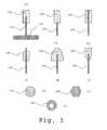
- FIG. 1is a sectional view of different configurations of funnel structures comprising one nanoelement with a volume element on top and three schematic cross sections of the nanoelement,
- FIG. 2is a sectional view of a funnel structure with a volume element with a low resistivity contact on the circumferential and top surfaces, arranged in a wrap around configuration on a nanoelement that is upstanding on a semiconductor substrate,
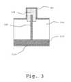
- FIG. 3is a sectional view of a semiconductor device comprising an intrinsic GaAs nanoelement, a p-type GaAs substrate underneath the nanoelement, a heavily n-doped InGaP volume element arranged in a wrap around configuration on the nanoelement, a SiO 2 layer surrounding the nanoelement and partly the volume element, and Ti/Au contacts deposited on both sides of the device, whereby a pn-junction is formed in the nanoelement,
- FIG. 4is a band diagram showing the energy levels in a funnel structure according to FIG. 3 , where the band gap of the volume element is larger than for the nanoelement,
- FIG. 5is a sectional view of EWIGFET in InAs, where the doping and diameter are designed so that the channel is closed at zero gate bias, and a volume element on top ensures a low access resistance,
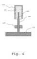
- FIG. 6is a sectional view of a FET device comprising an intrinsic GaAs nanoelement upstanding on a p + -GaP:Zn substrate with a gate electrode and a highly n-doped InGaP volume element arranged in a wrap around configuration on the nanoelement,
- FIG. 7is a sectional view of an array of FET devices according to FIG. 6 , however with the volume element arranged on top of the nanoelement,
- FIG. 8is a sectional view of an array of three identical LEDs comprising a p-GaAs nanoelement, upstanding on a p-GaP substrate, with a concentric layer of InGaP, a dielectric layer, e.g. SiO 2 enclosing the nanoelement, a n + -InGaP:Si volume element and a ITO contact deposited on the circumferential and top surfaces of the volume element,
- a dielectric layere.g. SiO 2
- FIG. 9is a sectional view of a semiconductor device intended for storing charge with a dielectric layer and conductive layer arranged on top of a nanoelement-volume element structure
- FIG. 10is a sectional view of a volume element (p)-nanoelement-volume element (n) structure
- FIG. 11is a schematic sectional view of a volume element (n)-nanoelement-volume element (n) structure and a volume element (p)-nanoelement-volume element (p) structure,
- FIG. 12is a funnel structure comprising a p+volume element in series with a intrinsic nanoelement and a n-type nanoelement, wherein the doping levels and dimensions are adjusted to have a pn-junction with essentially the whole depletion region located in the nanoelement, making it functional as a sensor,
- FIG. 13is a sectional view of a funnel structure with three heterostructure segments in a nanoelement extending with a volume element in contact with a semiconductor substrate enclosing the first heterostructure segment,
- FIG. 14is a scanning electron microscope micrograph showing a funnel structure according to FIG. 13 .
- FIG. 15is a cross sectional view of a volume element-nanoelement funnel structure with one nanoelement enclosed in the volume element and another nanoelement arranged on top of the volume element,
- FIG. 16is a scanning electron microscope micrograph showing a funnel structure according to FIG. 15 .
- FIG. 17is a sectional view of a volume element arranged on a relatively short nanoelement enabling lattice mismatch between the volume element and the substrate,
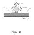
- FIG. 18is a cross sectional view of a volume element arranged on a short nanoelement contacting a patterned low resistivity layer on a substrate, and
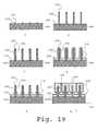
- FIG. 19is an illustration of one processing scheme for a LED device utilizing VLS growth of a nanoelement and growth of a volume element on top.
- a semiconductor deviceopens new possibilities for the implementation of different electronic and photonic semiconductor devices, particularly in small dimensions.
- the embodiments of present inventiondecrease general difficulties associated with doping of nanoelements, and to establish an alternative and feasible route to the doping of nanoelements, not only for when doping is complicated by the dimensions or the fabrication methods of such nanoelements, but also for providing new possibilities by the different prerequisites and for decreasing access resistances to electrical and optical devices made from nanoelements.
- nanoelement technologyin particular nanowire technology
- reasoning about nanoelements hereinafter mainlyis referred to the mentioned nanowire technology, in particular VLS grown nanowires
- the present inventionis, as appreciated by a skilled person, applicable on nanoelement semiconductor devices in general, irrespective of specific kind of nanoelements utilized.
- nanoelement formatin itself is not optimal from this perspective as the elongated nature and low area of the nanoelement cross-section will build device resistance.
- the main tools of fabricating low resistance contactsa task complicated by the intrinsically low contact-surfaces given by the nanoelement geometry, are high doping and low band gap adjustment on the semiconductor side of the contact, but as mentioned, the doping of nanoelements is challenged by several factors.
- the access to sufficient and accurate doping and a large contact surface without appreciably increasing device length and access resistancewould be beneficial for all types of semiconductor devices.
- the embodiments of the present inventionprovide a nanostructure, a so called funnel structure, comprising an epitaxial structure with at least one essentially one-dimensional nanoelement and at least one element extending in three dimensions, having a large volume and a large surface, hereinafter referred to as a volume element.
- a nanostructurea so called funnel structure
- the challenging doping procedures for nanoelementsmay be avoided, the processing is simplified and more reliable, the access resistance may be decreased, both due to doping and to an increased contact surface, the advantages of using a nanoelement may be utilized, and new applications and possibilities for nanoelement semiconductor devices open up.
- the funnel structurecomprises one nanoelement portion, possibly with all the attractive properties of such an element, and one epitaxially connected wider portion with an inherently large surface, a volume element portion, not necessarily of nanometer dimension adjacent to the nanoelement, where nanoelement properties are of less importance and rather bulk-like properties, enabling the volume element to easily be highly doped, are desired.
- the volume elementalthough not necessarily of nanometer dimension, may have some nanoelement properties, such as the ability to grow a crystalline structure with segments of different composition and without detrimental defects, not possible in using planar technology.
- the volume elementmay be a relatively thick shell that is epitaxially grown only around the one portion of the nanowire.
- the volume elementis preferably sufficiently thick and long such that it has bulk semiconductor like doping characteristics rather than 1D nanowire-like doping characteristics.
- the nanoelementmay have a diameter in the order of 100 nm to 500 nm, and the volume element a diameter in the order of 500 nm to 1000 nm, i.e. a thickness preferably on the order of 150 nm greater, such as about 200 nm.
- the funnel structureworks as a carrier reservoir enabling high carrier injection into the nanoelement from a region with well defined doping where low resistance contacts easily can be fabricated, preferably in a wrap around configuration in order to increase contact area and minimize distance between the nanoelement and the contact.
- the three-dimensional part of the funnelhas a certain volume and thickness, eliminating the challenges in doping of one-dimensional nanoelements, in order to achieve the necessary doping concentration and profiles, to decrease internal series resistance and contact resistance, increase carrier injection into the nanoelement, to establish desired built-in-voltage, and to provide a large contact surface.
- the low internal resistance and the increased amount of carriers due to the funnel natureprovide a high injection of majority carriers into the nanoelement already at low forward voltages.
- the funnel structuremay advantageously also be used as a light emitting diode or a pin detector (i.e., photodectotor based on a diode, such as p-i-n diode).
- the funnel structuremay be implemented in a nanoelement FET (field effect transistor) device wherein access resistance is decreased by utilizing funnel structures between drain/gate and/or source/gate.
- the increased surface area of a nanoelement device, due to a volume element,is not only important as means for reducing the access resistance, but also provides a large contact surface for a dielectric covering the volume element, enabling charge storage in e.g. a memory device. It is well known that the resistance arisen from the heterojunction discontinuity in valence or conduction band between two semiconductors or, similarly, the resistance from the Schottky barrier between a semiconductor and a metal can be decreased by high doping. The increased doping will decrease the width of the barrier and facilitate carriers to tunnel through the barrier effectively decreasing contact resistance.
- donor doped materialis n-type and acceptor doped material is p-type.
- the “n”indicates that electrons are charge carriers and consequently the “p” indicates that holes are the charge carriers.
- the pure and undoped materialis called intrinsic, but may naturally be n- or p-type.
- the conductivityis varied by adding different amount of dopants.
- a region that is highly dopedis in the figures and hereinafter denoted with a “+” sign.
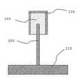
- the funnel structure of one embodimentcomprises a nanoelement 100 and a volume element 105 .
- the nanoelement 100comprises an intrinsic semiconductor (which may naturally be n or p-type as deposited) forming a first elongated cylinder
- the volume element 105comprises of a heavily doped semiconductor forming a second cylinder or sphere, with a larger diameter, epitaxially grown on one end portion of the nanoelement 100 .
- the volume element 105may be in a wrap around configuration where the volume element 105 partly encloses the nanoelement 100 end portion, such as the upper end portion, but does not enclose the lower portion of the nanoelement 100 adjacent to the substrate 110 .
- the funnel structureis commonly upstanding on the surface of a semiconductor substrate 110 .
- the funnel structuremay be upstanding at 90 degrees or at a different angle with respect to the substrate 110 .
- the volume element 105may be arranged in sequence ( 10 , 11 ) with the nanoelement 100 or the nanoelement 100 may extend through the volume element 105 , either continuing beyond ( 13 ) the volume element 105 or ending at the end ( 12 ) of the volume element 105 . Since different materials and processing may be employed to fabricate the nanoelements, different shapes are possible for the nanoelements.
- the volume elements 105can be cylindrical, rounded (mushroom shaped) ( 14 ), or slanted ( 15 ) at the part enclosing the nanoelement 100 .
- the cross-sections of the nanoelement 100 and the volume element 105 sare not necessarily circular ( 16 ), but may be polygonal. ( 17 ), such as hexagonal, due to the crystal structure of the material, or hollow ( 18 ).
- One embodiment of the present inventionis funnel structure, as illustrated in FIG. 2 , comprising, from the bottom, a nanoelement 100 of a semiconductor that is intrinsically p-type, upstanding on a semiconductor substrate 110 that is p-doped, forming a first elongated cylinder, with a diameter of about 100 nm and a length of about 2 ⁇ m, a heavily n-doped volume element 105 forming a second cylinder with an essentially larger diameter, i.e.
- volume element 105encloses the top portion, for example the upper 250 nm, of the nanoelement 100 in a wrapped around configuration, and a low resistance contact formed by a concentric layer 106 covering the top and mantle (side) surface(s) of the volume element 105 .
- the semiconductor substrate 110 in connection with the nanoelement 100is p-doped GaAs
- the nanoelement 100is an intrinsically p-type GaAs nanowire
- the volume element 105is n + -doped GaP
- the low resistivity contact 106is an ITO (InSnO) layer with a thickness of 10 nm. Due to the doped regions, a pn-junction is formed somewhere in the region between the substrate 110 and the volume element 105 .
- the dimensions given for the nanoelement 100 and volume element 105 in the embodimentsare by way of example only, and the length and diameter of the nanoelement and the diameter and height of the volume element 105 may be varied, within certain limits.
- the length of the nanoelement 100may be as short as a few epitaxial layers if the purpose of the nanoelement 100 only is to make it feasible to grow a three-dimensional volume element 105 on the substrate.
- the volume element 105 diameterpreferably is at least 50 nm wider than the diameter of the nanoelement 100 .
- the maximum diameter of the volume element 105is dependent on the device density.
- FIG. 3Another embodiment, shown in FIG. 3 , is a similar funnel structure to the foregoing example, comprising an intrinsic GaAs nanoelement 100 , a p-GaAs substrate 110 , a n + -InGaP volume element 105 , a filler layer 120 of SiO 2 (or another suitable insulating material) enclosing the whole nanoelement 100 and partly the volume element 105 , and thin film Ti/Au contacts ( 106 , 113 ) on the top surface of the structure and bottom surface of the substrate 110 respectively.
- the band diagramschematically illustrated in FIG. 4 , of such a funnel structure, shows the pn-junction formed in the nanoelement 100 with the volume element 105 and the substrate 110 respectively as the doped regions.
- the exact location and extension of the depletion zoneis dependent on the doping concentrations and profiles, geometry, etc.
- a p-type volume element 105 and an n-type one-dimensional nanoelement 100 and substrate 110e.g. a p-type volume element 105 and an n-type one-dimensional nanoelement 100 and substrate 110 .
- Suitable materials for the substrateinclude, but is not limited to, 110 Si, GaAs, GaP, GaP:Zn, GaAs, InAs, InP, GaN, Al 2 O 3 , SiC, Ge, GaSb, ZnO, InSb, SOI (silicon-on-insulator), CdS, ZnSe, CdTe, etc.
- Suitable materials for the nanoelements 100 and the volume elements 105include, bit is not limited to: GaAs (p), InAs, Ge, ZnO, InN, GaInN, GaN AlGaInN, BN, InP, InAsP, GaInP, InGaP:Si, InGaP:Zn, GaInAs, AlInP, GaAlInP, GaAlInAsP, GaInSb, InSb, Si, etc.
- Possible donor dopantsare, but not limited to, for e.g. GaP are Si, Sn, Te, Se, S, etc, and acceptor dopants for the same material are Zn, Fe, Mg, Be, Cd, etc.
- the doping levelis dependent on the type of semiconductor.
- GaAsis intrinsic at 10 16 cm ⁇ 3
- a typical doping level in the nanoelement 100is 10 16 -10 17 cm ⁇ 3 and 10 17 -10 20 in the volume element, depending on the dimensions and the conditions in the manufacturing process.
- measuring the doping level in nanoelementsis challenging and methods for measuring the doping level in nanoelements with high accuracy are not perfected at the present day.
- low resistivity contact materialsare dependent on the material to be deposited on, but metal, metal alloys as well as non-metal compounds like Al, Al—Si, TiSi 2 , TiN, W, MoSi 2 , PtSi, CoSi 2 , WSi 2 , In, AuGa, AuSb, AuGe, PdGe, Ti/Pt/Au, Ti/Al/Ti/Au, Pd/Au, ITO (InSnO), etc and combinations of e.g. metal and ITO can be used.
- the single and combination contactsare not limited to these materials.
- One embodiment of the present inventionis a semiconductor device, wherein a volume element 105 is arranged in a wrap around configuration on an end portion of a nanoelement 100 , as shown in FIG. 3 , and the nanoelement 100 is doped and has less than half of the donor or acceptor dopant concentration of the volume element 105 .
- One embodiment of the present inventionis a funnel structure according to FIG. 3 , wherein the generally one-dimensional nanoelement 100 is modulation doped by the volume element 105 .
- the volume element materialhas a higher band gap than the nanoelement material and due to the doping charge carriers diffuse from the volume element 105 into the nanoelement 100 . This is advantageous when doping in combination with high carrier mobility is needed.
- One embodiment of the present inventionis a semiconductor device comprising a nanoelement-volume element funnel structure, wherein the nanoelement 100 extends partly through the volume element 105 , i.e. a wrap around configuration, and wherein the nanoelement 100 changes composition, e.g. from GaAs to GaAsP, approximately where the volume element 105 begins.
- Another embodimentis based on a funnel structure comprising a volume element 105 on a nanoelement 100 with a wrap around configuration, wherein the volume element 105 composition gradually approaches or approximately has the same composition as the volume element 105 approximately where the volume element 105 begins.
- the composition of the nanoelement below the volume elementmay be different from the composition of the volume element.
- One embodiment of the present inventionis a semiconductor device comprising a nanoelement-volume element funnel structure, wherein the nanoelement 100 is doped to the same conductivity type as the volume element 105 . This may be necessary when the nanoelement 100 cannot be doped to the required doping level. An additional carrier injection from the volume element 105 is needed. In addition the access resistance is decreased.
- the nanoelements 100Due to the nanometer dimensions of the nanoelements 100 it is also possible to selectively change the composition along the length thereof, to grow a nanoelement of one composition onto a substrate 110 of another composition, and to form heterojunctions, with maintaining epitaxy despite a significant lattice mismatch. In particular, this allows for attaching a volume element 105 according to the embodiments of the present invention, which is otherwise not possible to grow on the substrate, to the substrate via a nanoelement 100 without introducing significant defects. Heterostructures along the length of the nanoelement 100 or in the volume element 105 may be introduced to enable the semiconductor device to carry out a desired function or to perform according to certain requirements.
- a heterostructure in a nanoelementcomprises at least two lengthwise segments of different composition and/or doping, a first segment of a first material and a second segment of a second material.
- An epitaxial boundaryis present between the first and the second segment, the boundary being limited to a number of lattice planes, wherein the composition or doping changes gradually.
- a heterostructure in a volume elementcomprises a plurality of concentric segments of different composition.
- the nanoelement 100can be doped to the same or different conductivity when compared to the three-dimensional volume element 105 .
- High doping and low band gap adjustment on the semiconductor side of the contactas mentioned, a usual tool for reducing the access resistance in common nanoelement devices, can be utilized also for the volume element 105 in the present invention.
- the doping level of the volume element 105may gradually change from the interface to the outer surface, i.e. gradient doping of the volume element 105 .
- heterostructures of the nanoelement 100 and/or the volume element 105comprising concentric layers of materials of different compositions and/or doping levels.
- a concentric layer of the nanoelement 100 or volume element 105can also be a dielectric material, or a low resistivity material, e.g. a metal, enclosing at least partly the nanoelement 100 or volume element 105 .
- modulation dopingmentioned above, of the nanoelement 100 can be obtained by use of a concentric layer of a doped semiconductor material with a higher band gap than the core material.
- Typical semiconductor material utilized in concentric layers of the nanoelement 100 and volume element 105are Ga/As/AlGaAS, AlSb, Si, GaP, InP, InAs, InGaP InPSb, GaInPSb, AlPSb, GaAsSb, InAsP, Al, AlAs, GaAlInAsP, etc.
- the choice of semiconductor materialsis not limited to these materials.
- One embodiment of the present invention that comprises heterostructures along the nanoelement 100 and a concentric layer on the nanoelement 100is an enhancement nanowire wrap insulating gate field effect transistor (EWIGFET), as illustrated in the schematic sectional view in FIG. 5 .
- the transistorcomprises a nanoelement, in this case a VLS grown nanowire, upstanding on a InAs substrate 110 , with a first n + -InAs nanoelement segment 100 a , a second intrinsic n-type InAs nanoelement segment 100 b and a third n + -InAs nanoelement segment 100 c , a thin concentric layer 101 of a dielectric material enclosing the part of the nanoelement segments 100 a , 100 b , 100 c that are not enclosed in a n + -InAs volume element 105 arranged on top of the nanoelement segment 100 c .
- EWIGFETenhancement nanowire wrap insulating gate field effect transistor
- a gate electrode 125 in a wrap around configurationis provided in between two filler layers 120 , 121 that fill the volume surrounding the nanoelement segments 100 a , 100 b , 100 c and partly also the volume element 105 .
- the dielectric material 101may act as a gate insulating layer between the gate 125 and the channel 100 b of the transistor.
- a thin film Ni contact 106is deposited on the top surface of the device.
- the volume element 105is utilized to decrease the access resistance partly by doping of the volume element 105 and partly by increasing the contact surface area.
- the nanoelement 100 in the EWIGFETis made of InAs, wherein the doping and diameter are designed so that the channel is closed at zero gate bias. However the same design applies to other materials than InAs, like InSb, InP, GaAs, Ge and Si.
- a DWIGFETis obtained when the doping levels are increased in such a way that the channel remains open at zero gate bias.
- the WIGFET structure described aboveis simplified and the challenging doping of the nanoelement 100 is excluded.
- an intrinsically p-type GaAs nanoelement 100with a portion of the nanoelement 100 enclosed in a thin concentric layer 101 of a dielectric material, e.g. SiO 2 , is upstanding on a p + -GaP:Zn substrate 110 with a n + InGaP volume element 105 arranged on top of the nanoelement 100 , enclosing the portion of the nanoelement that is not covered by the concentric layer 101 .
- a gate electrode 125is provided in a wrap around configuration along a small portion of the nanoelement 100 between the volume element 105 and the substrate 110 .
- the heavy doping of the volume element 105makes it a carrier reservoir for the undoped nanoelement 100 and creates a pn-junction in the nanoelement 100 .
- a voltage to the gate electrode 125a current flows in the nanoelement 100 .
- Layer 101functions as a gate insulating layer of the transistor. If the gate insulating layer is omitted, then a MESFET type transistor is formed.
- FIG. 7Another embodiment of the present invention, similar to the WIGFET structure described above, is a FET structure according to FIG. 7 .
- FIG. 7In this cross sectional view, an array of three FET structures is shown, wherein the volume element 105 is arranged on top of the nanoelement 100 instead of in a wrap around configuration as in FIG. 6 .
- the volume element 105is doped, either p or n type, in order to be one side of a pn-junction. This region has a certain volume and thickness in order to achieve the necessary doping concentration to decrease internal series resistance and contact resistance, increase carrier injection into the nanoelement 100 , while increasing built-in-voltage.
- the low internal resistance and the increased amount of carriers due to the funnel naturevouch for a high injection of majority carriers into the nanoelement 100 already at low forward voltages.
- High injection of carriers into the nanoelement 100introduces high concentrations of electron hole pairs into the nanoelement 100 increasing light emitting recombination.
- the high concentration of electron-hole pairsin combination with the active region being extended into a waveguide, directing the light, can enable stimulated emission, increasing the output of the device further.
- the nanoelement 100 material compositioncan be chosen to propagate into the volume element 105 in order to decrease the optical disturbance by the volume element-nanoelement connection. Extending the length of the nanoelement 100 in the direction of the emitted light will increase re-absorption. To decrease re-absorption the composition of the nanoelement 100 is adjusted in the direction of the emitted light in order to raise the band gap as compared to the energy of the emitted light.
- One embodiment of the present inventionis functional as a LED.
- An array of three identical such LEDsis shown in FIG. 8 .
- An undoped intrinsically p-type GaAs nanoelement 100 with length about 2 ⁇ m and diameter about 100 nm, upstanding on a p-doped GaP substrate 110is completely enclosed in a thin concentric layer 101 of InGaP.
- the concentric layer 101is utilized to optimize the wave guiding properties and acts as a cladding layer.
- An insulating and transparent masking material 115e.g. SiO 2 , covers about the lower half of the nanoelement 100 .
- an InGaP volume element 105Above this transparent masking material 115 and enclosing the nanoelement 100 there is an InGaP volume element 105 , with a diameter of about 500 nm and a length of about 1 ⁇ m, heavily doped with Si to obtain an n+-type material.
- a top electrode 106is deposited on the top surface and a bottom electrode 113 is deposited on the bottom side of the substrate 110 .
- the volume element 105 top surfaceis covered by a first concentric dielectric layer 106 in order to store a charge, e.g. for memory devices.
- this embodimentcomprises an intrinsic nanoelement 100 upstanding on a p-type semiconductor substrate 110 , a n-doped volume element 105 in a wrap around configuration, a concentric dielectric layer 101 enclosing the portion of the nanoelement 100 that is not enclosed by the volume element 105 , a dielectric material 906 deposited on the top and circumferential surfaces of the volume element 105 , a second concentric layer 107 , i.e. a top electrode on the dielectric material, and a wrap around gate electrode 125 .
- the stored chargecan be read out by applying a voltage to the gate electrode 125 .
- the charge storage dielectricmay comprise an a capacitor dielectric such that a capacitor is located in electrical contact with the transistor (i.e., a DRAM-type configuration).
- the nanoelement-volume element sequencemay be repeated along the nanoelement 100 .
- a first n-doped volume element 105 a and second p-doped volume element 105 bshare a common nanoelement 100 in-between, forming a volume element (p)-nanoelement-volume element (n) structure, shown in FIG. 10 .
- a structuremay advantageously be implemented in LEDs and diodes or as emitter-base and base-collector junctions in hetero-bipolar transistors.
- Another embodimentis when a first volume element 105 a and second volume element 105 b of common conductivity type (n or p and individually ohmically connected to a circuitry) are connected through a nanoelement 100 where a non-ohmic terminal altogether forming a volume element (n)-nanoelement-volume element (n) or volume element (p)-nanoelement-volume element (p) structure, as shown in FIG. 11 , whereby charge carriers of the proper type are injected into the nanoelement 100 .
- this structurecomprises two volume elements 105 a , 105 b , one n-type volume element 105 b at the bottom, in conjunction with the substrate 110 , and one p + -type volume element 105 a arranged in a wrap around configuration on top of the nanoelement 100 that is upstanding on the substrate 110 and extending through the lower volume element 105 b .
- a pn-junctionis formed and the volume of the active region, i.e. the depletion region, appreciably coincides with the one-dimensional region in the funnel structure, close to the junction between the nanoelement 100 and the upper volume element 105 a .
- the one-dimensional regionis easily depleted due to low doping ion concentration and low volume, since the total amount of charge moved is low.
- the high doping concentration together with a larger volume of the volume elements 105 a , 105 bgives that the depletion region will protrude into less volume and, especially, less distance in the direction of transport in the volume element 105 a .
- One embodiment comprising a heterostructure in the one dimensional nanoelement 100is a funnel structure as the one shown in the schematic drawing in FIG. 13 and in the scanning electron microscope micrograph in FIG. 14 .
- a one-dimensional nanoelementcomprising a first nanoelement segment 100 a of GaP, a second nanoelement segment 100 b of GaAsP and a third nanoelement segment 100 c of GaP, is upstanding on a semiconductor substrate 110 .
- the first segment 100 ais fully enclosed in a three-dimensional GaP volume element 105 .
- This structuredecreases the injection resistance from the substrate 110 into the nanoelement segment 100 a .
- a similar structureis the funnel structure shown in the schematic drawing in FIG. 15 and in the scanning electron microscope micrograph in FIG. 16 , providing another embodiment of the present invention, wherein a first one-dimensional nanoelement 100 a made of GaAsP is enclosed, both on the cylindrical mantle surface and on the top, by an InGaP volume element 105 .
- the one-dimensional nanoelement 100 b visible in FIG. 16is grown on top of the volume element 105 .
- FIG. 17Another embodiment, similar to the embodiments referring to FIGS. 13 and 15 above, is shown in FIG. 17 .
- a patterned low resistivity layer 118such as conductor or electrode, preferably a metal layer, is provided on the substrate 110 .
- Layer 118contains a small hole.
- a nanoelement segment 100 afills up the hole and protrudes sufficiently to enable radial growth of the volume element 105 that is enclosing the nanoelement segment 100 a , whereby the volume element 105 forms an ohmic contact between the low resistivity layer 118 and the semiconductor device.
- a second nanoelement segment 100 bis upstanding from the volume element 105 .
- this embodimentis useful when a non-conducting substrate is used and a metallic contact, preferably lithographically defined, is desired to a single crystal or high quality polycrystalline semiconductor volume element.
- Another embodiment of the present inventionis a light emitting device, where the nanoelement's main function is to provide a good heterojunction between a substrate 110 and a volume element 105 that normally are impossible to combine due to too large lattice mismatch, i.e. the nanoelement 100 is utilized as a very thin template bridging the incompatible materials.
- an undoped InGaN nanoelement 100is grown on a n + GaN/Sapphire substrate 110 through a silicon nitride mask 115 allowing for a p + GaN volume element 105 on top with an optional contact 106 .
- a method of fabricating funnel structuresis to first grow a nanoelement 100 , mask the intended nanoelement 100 with a masking layer 115 and re-grow selectively the intended volume element 105 , as shown in FIG. 19 .
- the volume element 105grows both in axial and radial directions. Hence, when the nanoelement 100 is masked partly, the nanoelement 100 becomes enclosed in the volume element 105 .
- Appropriate masking materialsare e.g. silicon nitride, silicon oxide, etc.
- nanoelement growthis locally enhanced by a substance, as VLS grown nanowires
- the ability to alter between radial and axial growth by altering growth conditionsenables the procedure (nanowire growth, mask formation, and subsequent selective growth) that can be repeated to form nanoelement-volume element sequences of higher order.
- nanoelement growth and selective growthare not distinguished by separate growth conditions it may be better to first grow the nanoelement 100 along the length and by different selective growth steps grow different types of volume element 105 regions.
- a fabrication method according to the embodiment of the present inventionwill be exemplified with the fabrication of a light emitting pn-diode/array with active nanowire region(s), illustrated in FIG. 19 .
- the methodcomprises the steps of:
- the volume elementis either doped ( 8 ) during the growth or afterwards (not shown).
- Concentric layers ( 106 , 101 )may optionally be grown both on the volume element ( 105 ) and the nanoelement ( 100 ).
Landscapes
- Engineering & Computer Science (AREA)
- Physics & Mathematics (AREA)
- Manufacturing & Machinery (AREA)
- Microelectronics & Electronic Packaging (AREA)
- Power Engineering (AREA)
- Condensed Matter Physics & Semiconductors (AREA)
- General Physics & Mathematics (AREA)
- Computer Hardware Design (AREA)
- Chemical & Material Sciences (AREA)
- Nanotechnology (AREA)
- Crystallography & Structural Chemistry (AREA)
- Materials Engineering (AREA)
- Mathematical Physics (AREA)
- Theoretical Computer Science (AREA)
- Electrodes Of Semiconductors (AREA)
- Led Devices (AREA)
Abstract
Description
- 1. definition of local catalyst/
catalyst islands 130 on ap+ GaP substrate 110 by lithography, - 2.
GaAs nanowire 100 growth from thelocal catalyst islands 130, - 3. radial growth of thin InGaP
concentric layer 101 around thenanowire 100, - 4. deposition of SiO2as a
mask material 115, - 5. partial etch back of
mask 115 to expose the upper parts of thenanowires 100, - 6. selective epitaxial growth of n+
InGaP volume element 105, and - 7. contact106,113 formation on the volume element and to the substrate, respectively.
- 1. definition of local catalyst/
Claims (33)
Priority Applications (6)
| Application Number | Priority Date | Filing Date | Title |
|---|---|---|---|
| EP07861100AEP2095426A4 (en) | 2006-12-22 | 2007-12-22 | NANOELECTRIC STRUCTURE AND MANUFACTURING METHOD THEREFOR |
| PCT/SE2007/001171WO2008079077A2 (en) | 2006-12-22 | 2007-12-22 | Nanoelectronic structure and method of producing such |
| US12/662,962US8067299B2 (en) | 2006-12-22 | 2010-05-13 | Nanoelectronic structure and method of producing such |
| US13/227,950US8455857B2 (en) | 2006-12-22 | 2011-09-08 | Nanoelectronic structure and method of producing such |
| US13/886,478US8796119B2 (en) | 2006-12-22 | 2013-05-03 | Nanoelectronic structure and method of producing such |
| US14/323,340US9096429B2 (en) | 2006-12-22 | 2014-07-03 | Nanoelectronic structure and method of producing such |
Applications Claiming Priority (3)
| Application Number | Priority Date | Filing Date | Title |
|---|---|---|---|
| SE0602840 | 2006-12-22 | ||
| SE0602840-1 | 2006-12-22 | ||
| SE0602840 | 2006-12-22 |
Related Child Applications (2)
| Application Number | Title | Priority Date | Filing Date |
|---|---|---|---|
| US12/662,962DivisionUS8067299B2 (en) | 2006-12-22 | 2010-05-13 | Nanoelectronic structure and method of producing such |
| US13/227,950ContinuationUS8455857B2 (en) | 2006-12-22 | 2011-09-08 | Nanoelectronic structure and method of producing such |
Publications (2)
| Publication Number | Publication Date |
|---|---|
| US20080149914A1 US20080149914A1 (en) | 2008-06-26 |
| US8049203B2true US8049203B2 (en) | 2011-11-01 |
Family
ID=39541533
Family Applications (5)
| Application Number | Title | Priority Date | Filing Date |
|---|---|---|---|
| US11/812,226Expired - Fee RelatedUS8049203B2 (en) | 2006-12-22 | 2007-06-15 | Nanoelectronic structure and method of producing such |
| US12/662,962Expired - Fee RelatedUS8067299B2 (en) | 2006-12-22 | 2010-05-13 | Nanoelectronic structure and method of producing such |
| US13/227,950Expired - Fee RelatedUS8455857B2 (en) | 2006-12-22 | 2011-09-08 | Nanoelectronic structure and method of producing such |
| US13/886,478Expired - Fee RelatedUS8796119B2 (en) | 2006-12-22 | 2013-05-03 | Nanoelectronic structure and method of producing such |
| US14/323,340Expired - Fee RelatedUS9096429B2 (en) | 2006-12-22 | 2014-07-03 | Nanoelectronic structure and method of producing such |
Family Applications After (4)
| Application Number | Title | Priority Date | Filing Date |
|---|---|---|---|
| US12/662,962Expired - Fee RelatedUS8067299B2 (en) | 2006-12-22 | 2010-05-13 | Nanoelectronic structure and method of producing such |
| US13/227,950Expired - Fee RelatedUS8455857B2 (en) | 2006-12-22 | 2011-09-08 | Nanoelectronic structure and method of producing such |
| US13/886,478Expired - Fee RelatedUS8796119B2 (en) | 2006-12-22 | 2013-05-03 | Nanoelectronic structure and method of producing such |
| US14/323,340Expired - Fee RelatedUS9096429B2 (en) | 2006-12-22 | 2014-07-03 | Nanoelectronic structure and method of producing such |
Country Status (1)
| Country | Link |
|---|---|
| US (5) | US8049203B2 (en) |
Cited By (38)
| Publication number | Priority date | Publication date | Assignee | Title |
|---|---|---|---|---|
| US20110316019A1 (en)* | 2006-12-22 | 2011-12-29 | Qunano Ab | Nanoelectronic Structure and Method of Producing Such |
| US20120153124A1 (en)* | 2010-12-21 | 2012-06-21 | Zena Technologies, Inc. | Vertically structured passive pixel arrays and methods for fabricating the same |
| US8710488B2 (en)* | 2009-12-08 | 2014-04-29 | Zena Technologies, Inc. | Nanowire structured photodiode with a surrounding epitaxially grown P or N layer |
| US8735797B2 (en) | 2009-12-08 | 2014-05-27 | Zena Technologies, Inc. | Nanowire photo-detector grown on a back-side illuminated image sensor |
| US8748799B2 (en) | 2010-12-14 | 2014-06-10 | Zena Technologies, Inc. | Full color single pixel including doublet or quadruplet si nanowires for image sensors |
| US8766272B2 (en) | 2009-12-08 | 2014-07-01 | Zena Technologies, Inc. | Active pixel sensor with nanowire structured photodetectors |
| US8791470B2 (en) | 2009-10-05 | 2014-07-29 | Zena Technologies, Inc. | Nano structured LEDs |
| US8810808B2 (en) | 2009-05-26 | 2014-08-19 | Zena Technologies, Inc. | Determination of optimal diameters for nanowires |
| US8835905B2 (en) | 2010-06-22 | 2014-09-16 | Zena Technologies, Inc. | Solar blind ultra violet (UV) detector and fabrication methods of the same |
| US8866065B2 (en) | 2010-12-13 | 2014-10-21 | Zena Technologies, Inc. | Nanowire arrays comprising fluorescent nanowires |
| US8890271B2 (en) | 2010-06-30 | 2014-11-18 | Zena Technologies, Inc. | Silicon nitride light pipes for image sensors |
| US8889455B2 (en) | 2009-12-08 | 2014-11-18 | Zena Technologies, Inc. | Manufacturing nanowire photo-detector grown on a back-side illuminated image sensor |
| US20140346558A1 (en)* | 2013-05-21 | 2014-11-27 | Daegu Gyeongbuk Institute Of Science & Technology | Rectifying device and method for manufacturing the same |
| US9000353B2 (en) | 2010-06-22 | 2015-04-07 | President And Fellows Of Harvard College | Light absorption and filtering properties of vertically oriented semiconductor nano wires |
| US20150137079A1 (en)* | 2012-07-19 | 2015-05-21 | Taiwan Semiconductor Manufacturing Company Limited | Vertical tunnel field effect transistor (fet) |
| US9082673B2 (en) | 2009-10-05 | 2015-07-14 | Zena Technologies, Inc. | Passivated upstanding nanostructures and methods of making the same |
| US20150279672A1 (en)* | 2012-10-26 | 2015-10-01 | Aledia | Process for growing at least one nanowire using a transition metal nitride layer obtained in two steps |
| US9177985B2 (en) | 2009-06-04 | 2015-11-03 | Zena Technologies, Inc. | Array of nanowires in a single cavity with anti-reflective coating on substrate |
| US20150325695A1 (en)* | 2014-05-09 | 2015-11-12 | SK Hynix Inc. | Semiconductor apparatus, method for fabricating the same, and variable resistive memory device |
| US9287516B2 (en)* | 2014-04-07 | 2016-03-15 | International Business Machines Corporation | Forming pn junction contacts by different dielectrics |
| US9299866B2 (en) | 2010-12-30 | 2016-03-29 | Zena Technologies, Inc. | Nanowire array based solar energy harvesting device |
| US9304035B2 (en) | 2008-09-04 | 2016-04-05 | Zena Technologies, Inc. | Vertical waveguides with various functionality on integrated circuits |
| US9318655B2 (en) | 2006-12-22 | 2016-04-19 | Qunano Ab | Elevated LED |
| US9343490B2 (en) | 2013-08-09 | 2016-05-17 | Zena Technologies, Inc. | Nanowire structured color filter arrays and fabrication method of the same |
| US9406709B2 (en) | 2010-06-22 | 2016-08-02 | President And Fellows Of Harvard College | Methods for fabricating and using nanowires |
| US9429723B2 (en) | 2008-09-04 | 2016-08-30 | Zena Technologies, Inc. | Optical waveguides in image sensors |
| US9478685B2 (en) | 2014-06-23 | 2016-10-25 | Zena Technologies, Inc. | Vertical pillar structured infrared detector and fabrication method for the same |
| US9515218B2 (en) | 2008-09-04 | 2016-12-06 | Zena Technologies, Inc. | Vertical pillar structured photovoltaic devices with mirrors and optical claddings |
| US20170012126A1 (en)* | 2014-03-28 | 2017-01-12 | Intel Corporation | Selectively regrown top contact for vertical semiconductor devices |
| US9680039B2 (en) | 2002-07-08 | 2017-06-13 | Qunano Ab | Nanostructures and methods for manufacturing the same |
| US9679966B2 (en) | 2012-10-26 | 2017-06-13 | Commissariat A L'energie Atomique Et Aux Energies Alternatives | Electronic device containing nanowire(s), equipped with a transition metal buffer layer, process for growing at least one nanowire, and process for manufacturing a device |
| US20170278927A1 (en)* | 2016-03-23 | 2017-09-28 | Globalfoundries Inc. | High density memory cell structures |
| US20180090350A1 (en)* | 2016-09-28 | 2018-03-29 | Stmicroelectronics S.R.L. | Apparatus for manufacturing a silicon carbide wafer |
| US10263149B2 (en) | 2006-12-22 | 2019-04-16 | Qunano Ab | Nanostructured LED array with collimating reflectors |
| US10319926B2 (en) | 2015-11-05 | 2019-06-11 | International Business Machines Corporation | End-bonded metal contacts on carbon nanotubes |
| US10828400B2 (en) | 2014-06-10 | 2020-11-10 | The Research Foundation For The State University Of New York | Low temperature, nanostructured ceramic coatings |
| US11830724B2 (en) | 2018-11-06 | 2023-11-28 | Stmicroelectronics S.R.L. | Apparatus and method for manufacturing a wafer |
| US11946158B2 (en) | 2019-09-03 | 2024-04-02 | Stmicroelectronics S.R.L. | Apparatus for growing a semiconductor wafer and associated manufacturing process |
Families Citing this family (50)
| Publication number | Priority date | Publication date | Assignee | Title |
|---|---|---|---|---|
| US8178403B2 (en)* | 2006-09-18 | 2012-05-15 | Qunano Ab | Method of producing precision vertical and horizontal layers in a vertical semiconductor structure |
| EP2064744A2 (en)* | 2006-09-19 | 2009-06-03 | QuNano AB | Assembly of nanoscaled field effect transistors |
| KR101361129B1 (en)* | 2007-07-03 | 2014-02-13 | 삼성전자주식회사 | luminous device and method of manufacturing the same |
| JP5524839B2 (en) | 2007-08-21 | 2014-06-18 | ザ、リージェンツ、オブ、ザ、ユニバーシティ、オブ、カリフォルニア | Thermoelectric device with nanostructures and method of operating the device |
| KR101436000B1 (en)* | 2008-02-22 | 2014-08-29 | 삼성전자주식회사 | Nano- or micro-sized diodes and methods of making the same |
| JP5453406B2 (en)* | 2008-06-13 | 2014-03-26 | クナノ アーベー | Nanostructured MOS capacitor |
| JP4530098B1 (en)* | 2009-05-29 | 2010-08-25 | 日本ユニサンティスエレクトロニクス株式会社 | Semiconductor device |
| US8211735B2 (en)* | 2009-06-08 | 2012-07-03 | International Business Machines Corporation | Nano/microwire solar cell fabricated by nano/microsphere lithography |
| JP2011040421A (en) | 2009-08-06 | 2011-02-24 | Elpida Memory Inc | Semiconductor device and method of manufacturing the same |
| EP2472585B1 (en)* | 2009-09-30 | 2022-07-06 | National University Corporation Hokkaido University | Tunnel field effect transistor and method for manufacturing same |
| US8129247B2 (en) | 2009-12-04 | 2012-03-06 | International Business Machines Corporation | Omega shaped nanowire field effect transistors |
| US8173993B2 (en)* | 2009-12-04 | 2012-05-08 | International Business Machines Corporation | Gate-all-around nanowire tunnel field effect transistors |
| US8384065B2 (en)* | 2009-12-04 | 2013-02-26 | International Business Machines Corporation | Gate-all-around nanowire field effect transistors |
| US8143113B2 (en)* | 2009-12-04 | 2012-03-27 | International Business Machines Corporation | Omega shaped nanowire tunnel field effect transistors fabrication |
| US8097515B2 (en)* | 2009-12-04 | 2012-01-17 | International Business Machines Corporation | Self-aligned contacts for nanowire field effect transistors |
| US8455334B2 (en) | 2009-12-04 | 2013-06-04 | International Business Machines Corporation | Planar and nanowire field effect transistors |
| US8722492B2 (en) | 2010-01-08 | 2014-05-13 | International Business Machines Corporation | Nanowire pin tunnel field effect devices |
| US8324940B2 (en) | 2010-04-13 | 2012-12-04 | International Business Machines Corporation | Nanowire circuits in matched devices |
| US8361907B2 (en) | 2010-05-10 | 2013-01-29 | International Business Machines Corporation | Directionally etched nanowire field effect transistors |
| US8324030B2 (en) | 2010-05-12 | 2012-12-04 | International Business Machines Corporation | Nanowire tunnel field effect transistors |
| JP5841752B2 (en)* | 2010-07-02 | 2016-01-13 | 株式会社半導体エネルギー研究所 | Semiconductor device |
| US8835231B2 (en) | 2010-08-16 | 2014-09-16 | International Business Machines Corporation | Methods of forming contacts for nanowire field effect transistors |
| KR101636915B1 (en)* | 2010-09-03 | 2016-07-07 | 삼성전자주식회사 | Semiconductor compound structure and method of manufacturing the same using graphene or carbon nanotubes, and seciconductor device including the semiconductor compound |
| WO2012035243A1 (en)* | 2010-09-14 | 2012-03-22 | Commissariat A L'energie Atomique Et Aux Energies Alternatives | Nanowire-based optoelectronic device for light emission |
| US8536563B2 (en) | 2010-09-17 | 2013-09-17 | International Business Machines Corporation | Nanowire field effect transistors |
| US9240328B2 (en) | 2010-11-19 | 2016-01-19 | Alphabet Energy, Inc. | Arrays of long nanostructures in semiconductor materials and methods thereof |
| US8736011B2 (en) | 2010-12-03 | 2014-05-27 | Alphabet Energy, Inc. | Low thermal conductivity matrices with embedded nanostructures and methods thereof |
| WO2012088085A1 (en)* | 2010-12-21 | 2012-06-28 | Alphabet Energy, Inc. | Arrays of filled nanostructures with protruding segments and methods thereof |
| CA2825888A1 (en)* | 2011-02-02 | 2012-11-29 | Alphabet Energy, Inc. | Electrode structures for arrays of nanostructures and methods thereof |
| US9035278B2 (en) | 2011-09-26 | 2015-05-19 | Glo Ab | Coalesced nanowire structures with interstitial voids and method for manufacturing the same |
| US8350249B1 (en)* | 2011-09-26 | 2013-01-08 | Glo Ab | Coalesced nanowire structures with interstitial voids and method for manufacturing the same |
| US9051175B2 (en) | 2012-03-07 | 2015-06-09 | Alphabet Energy, Inc. | Bulk nano-ribbon and/or nano-porous structures for thermoelectric devices and methods for making the same |
| US10090292B2 (en) | 2012-07-06 | 2018-10-02 | Qunano Ab | Radial nanowire Esaki diode devices and methods |
| US9142400B1 (en) | 2012-07-17 | 2015-09-22 | Stc.Unm | Method of making a heteroepitaxial layer on a seed area |
| US9257627B2 (en) | 2012-07-23 | 2016-02-09 | Alphabet Energy, Inc. | Method and structure for thermoelectric unicouple assembly |
| US9082930B1 (en) | 2012-10-25 | 2015-07-14 | Alphabet Energy, Inc. | Nanostructured thermolectric elements and methods of making the same |
| US8937294B2 (en) | 2013-03-15 | 2015-01-20 | Rohm And Haas Electronic Materials Llc | Multi-heterojunction nanoparticles, methods of manufacture thereof and articles comprising the same |
| WO2015016851A1 (en)* | 2013-07-31 | 2015-02-05 | Hewlett-Packard Development Company, L.P. | Memristor and methods for making the same |
| US9634114B2 (en)* | 2013-08-13 | 2017-04-25 | National University Corporation Hakkaido University | Tunnel field-effect transistor, method for manufacturing same, and switch element |
| WO2015157501A1 (en) | 2014-04-10 | 2015-10-15 | Alphabet Energy, Inc. | Ultra-long silicon nanostructures, and methods of forming and transferring the same |
| US9786774B2 (en)* | 2014-06-27 | 2017-10-10 | Taiwan Semiconductor Manufacturing Company, Ltd. | Metal gate of gate-all-around transistor |
| KR102198694B1 (en) | 2014-07-11 | 2021-01-06 | 삼성전자주식회사 | Semiconductor light emitting device and manufacturing method of the same |
| US9425324B2 (en)* | 2014-09-30 | 2016-08-23 | Taiwan Semiconductor Manufacturing Company Limited | Semiconductor device and channel structure thereof |
| WO2016069831A1 (en)* | 2014-10-30 | 2016-05-06 | President And Fellows Of Harvard College | Nanoscale wires with tip-localized junctions |
| US9460921B2 (en)* | 2015-04-06 | 2016-10-04 | The United States Of America, As Represented By The Secretary Of Commerce | Nanowire article and processes for making and using same |
| US9755013B2 (en) | 2015-04-22 | 2017-09-05 | Globalfoundries Inc. | High density capacitor structure and method |
| US10483105B2 (en) | 2015-05-13 | 2019-11-19 | Stc.Unm | Nanowire bending for planar device process on (001) Si substrates |
| JP6375316B2 (en)* | 2016-01-06 | 2018-08-15 | ユニサンティス エレクトロニクス シンガポール プライベート リミテッドUnisantis Electronics Singapore Pte Ltd. | Semiconductor device manufacturing method and semiconductor device |
| FR3048817B1 (en)* | 2016-03-11 | 2018-06-15 | Valeo Comfort And Driving Assistance | SCREEN AND HIGH HEAD DISPLAY INCLUDING SUCH SCREEN |
| KR20250065040A (en)* | 2023-11-03 | 2025-05-12 | 삼성전자주식회사 | Semiconductor device |
Citations (75)
| Publication number | Priority date | Publication date | Assignee | Title |
|---|---|---|---|---|
| EP0443920A1 (en) | 1990-02-23 | 1991-08-28 | Thomson-Csf | Process for the controlled growth of needle-like crystals and their application for making pointed microcathodes |
| US5196396A (en) | 1991-07-16 | 1993-03-23 | The President And Fellows Of Harvard College | Method of making a superconducting fullerene composition by reacting a fullerene with an alloy containing alkali metal |
| EP0544408A2 (en) | 1991-10-28 | 1993-06-02 | Xerox Corporation | Quantum confinement semiconductor light emitting devices |
| US5252835A (en) | 1992-07-17 | 1993-10-12 | President And Trustees Of Harvard College | Machining oxide thin-films with an atomic force microscope: pattern and object formation on the nanometer scale |
| US5332910A (en) | 1991-03-22 | 1994-07-26 | Hitachi, Ltd. | Semiconductor optical device with nanowhiskers |
| US5362972A (en) | 1990-04-20 | 1994-11-08 | Hitachi, Ltd. | Semiconductor device using whiskers |
| US5381753A (en) | 1992-04-30 | 1995-01-17 | Matsushita Electric Industrial Co., Ltd. | Fabrication method of fine structures |
| WO1995002709A2 (en) | 1993-07-15 | 1995-01-26 | President And Fellows Of Harvard College | EXTENDED NITRIDE MATERIAL COMPRISING β-C3N¿4? |
| US5544617A (en) | 1992-05-22 | 1996-08-13 | Denki Kagaku Kogyo Kabushiki Kaisha | Method for producing single crystal, and needle-like single crystal |
| WO1997031139A1 (en) | 1996-02-26 | 1997-08-28 | President And Fellows Of Harvard College | Metal oxide nanorods |
| EP0838865A2 (en) | 1996-10-28 | 1998-04-29 | Sony Corporation | Quantum wires formed on a substrate, manufacturing method thereof, and device having quantum wires on a substrate |
| US5858862A (en) | 1996-09-25 | 1999-01-12 | Sony Corporation | Process for producing quantum fine wire |
| US5897945A (en) | 1996-02-26 | 1999-04-27 | President And Fellows Of Harvard College | Metal oxide nanorods |
| US5899734A (en) | 1997-06-04 | 1999-05-04 | Lg Semicon Co., Ltd. | Method of fabricating semiconductor device |
| US5997832A (en) | 1997-03-07 | 1999-12-07 | President And Fellows Of Harvard College | Preparation of carbide nanorods |
| JP2000068493A (en) | 1998-08-24 | 2000-03-03 | Sony Corp | Semiconductor element having quantum structure and manufacture thereof |
| US6159742A (en) | 1998-06-05 | 2000-12-12 | President And Fellows Of Harvard College | Nanometer-scale microscopy probes |
| WO2001003208A1 (en) | 1999-07-02 | 2001-01-11 | President And Fellows Of Harvard College | Nanoscopic wire-based devices, arrays, and methods of their manufacture |
| US6190634B1 (en) | 1995-06-07 | 2001-02-20 | President And Fellows Of Harvard College | Carbide nanomaterials |
| WO2001077726A1 (en) | 2000-04-06 | 2001-10-18 | Btg International Limited | Optical device |
| US6307241B1 (en) | 1995-06-07 | 2001-10-23 | The Regents Of The Unversity Of California | Integrable ferromagnets for high density storage |
| WO2001084238A1 (en) | 2000-05-04 | 2001-11-08 | Btg International Limited | Nanostructures |
| WO2002001648A1 (en) | 2000-06-28 | 2002-01-03 | Motorola, Inc. | Semiconductor structure, device, circuit, and process |
| US6340822B1 (en) | 1999-10-05 | 2002-01-22 | Agere Systems Guardian Corp. | Article comprising vertically nano-interconnected circuit devices and method for making the same |
| WO2002017362A2 (en) | 2000-08-22 | 2002-02-28 | President And Fellows Of Harvard College | Doped elongated semiconductors, growing such semiconductors, devices including such semiconductors and fabricating such devices |
| WO2002048701A2 (en) | 2000-12-11 | 2002-06-20 | President And Fellows Of Harvard College | Nanosensors |
| EP1221722A1 (en) | 2001-01-06 | 2002-07-10 | Interuniversitair Microelektronica Centrum Vzw | Highly efficient paraboloid light emitting diode |
| US20020129761A1 (en) | 2001-01-18 | 2002-09-19 | Tomohide Takami | Nanofiber and method of manufacturing nanofiber |
| US6455340B1 (en) | 2001-12-21 | 2002-09-24 | Xerox Corporation | Method of fabricating GaN semiconductor structures using laser-assisted epitaxial liftoff |
| WO2002080280A1 (en) | 2001-03-30 | 2002-10-10 | The Regents Of The University Of California | Methods of fabricating nanostructures and nanowires and devices fabricated therefrom |
| WO2002095883A2 (en) | 2001-05-23 | 2002-11-28 | Novalux, Inc. | Wavelength selectable, controlled chirp, semiconductor laser |
| WO2003005450A2 (en) | 2001-05-18 | 2003-01-16 | President And Fellows Of Harvard College | Nanoscale wires and related devices |
| US6559468B1 (en) | 1999-03-29 | 2003-05-06 | Hewlett-Packard Development Company Lp | Molecular wire transistor (MWT) |
| US20030089899A1 (en) | 2000-08-22 | 2003-05-15 | Lieber Charles M. | Nanoscale wires and related devices |
| US6586965B2 (en) | 2001-10-29 | 2003-07-01 | Hewlett Packard Development Company Lp | Molecular crossbar latch |
| US20030121764A1 (en) | 2001-12-27 | 2003-07-03 | The Regents Of The University Of California | Nanowire optoelectric switching device and method |
| WO2003053851A2 (en) | 2001-07-20 | 2003-07-03 | President And Fellows Of Harvard College | Transition metal oxide nanowires |
| US6596377B1 (en)* | 2000-03-27 | 2003-07-22 | Science & Technology Corporation @ Unm | Thin film product and method of forming |
| WO2003063208A2 (en) | 2002-01-18 | 2003-07-31 | California Institute Of Technology | Array-based architecture for molecular electronics |
| WO2004010552A1 (en) | 2002-07-19 | 2004-01-29 | President And Fellows Of Harvard College | Nanoscale coherent optical components |
| US6693021B1 (en)* | 1997-10-30 | 2004-02-17 | Sumitomo Electric Industries, Ltd. | GaN single crystal substrate and method of making the same |
| US6709929B2 (en)* | 2001-06-25 | 2004-03-23 | North Carolina State University | Methods of forming nano-scale electronic and optoelectronic devices using non-photolithographically defined nano-channel templates |
| US6716409B2 (en) | 2000-09-18 | 2004-04-06 | President And Fellows Of The Harvard College | Fabrication of nanotube microscopy tips |
| US6743408B2 (en) | 2000-09-29 | 2004-06-01 | President And Fellows Of Harvard College | Direct growth of nanotubes, and their use in nanotweezers |
| US20040109666A1 (en)* | 2002-12-10 | 2004-06-10 | John Kim | Optoelectronic devices employing fibers for light collection and emission |
| US20040175844A1 (en) | 2002-12-09 | 2004-09-09 | The Regents Of The University Of California | Sacrificial template method of fabricating a nanotube |
| US20040252737A1 (en) | 2003-06-16 | 2004-12-16 | Gyu Chul Yi | Zinc oxide based nanorod with quantum well or coaxial quantum structure |
| US20040262636A1 (en)* | 2002-12-09 | 2004-12-30 | The Regents Of The University Of California | Fluidic nanotubes and devices |
| US20050006673A1 (en)* | 2003-04-04 | 2005-01-13 | Btg International Limited | Nanowhiskers with PN junctions, doped nanowhiskers, and methods for preparing them |
| US20050011431A1 (en) | 2003-04-04 | 2005-01-20 | Btg International Limited | Precisely positioned nanowhiskers and nanowhisker arrays and method for preparing them |
| US20050017171A1 (en) | 2003-07-08 | 2005-01-27 | Btg International Limited | Probe structures incorporating nanowhiskers, production methods thereof and methods of forming nanowhiskers |
| US20050199886A1 (en) | 2004-03-10 | 2005-09-15 | Siltron Inc. | Nitride semiconductor device and method of manufacturing the same |
| US20050224790A1 (en)* | 2004-04-07 | 2005-10-13 | Samsung Electronics Co., Ltd. | Nanowire light emitting device and method of fabricating the same |
| US20060019470A1 (en) | 2004-02-06 | 2006-01-26 | Btg International Limited | Directionally controlled growth of nanowhiskers |
| US20060057360A1 (en) | 2003-11-26 | 2006-03-16 | Samuelson Lars I | Nanostructures formed of branched nanowhiskers and methods of producing the same |
| US20060073680A1 (en)* | 2004-08-20 | 2006-04-06 | Jung Han | Epitaxial growth of aligned algainn nanowires by metal-organic chemical vapor deposition |
| US20060112466A1 (en)* | 2002-12-13 | 2006-05-25 | Canon Kabushiki Kaisha | Nanostructure, electronic device and method of manufacturing the same |
| US20060125056A1 (en) | 2004-06-25 | 2006-06-15 | Btg International Limited | Formation of nanowhiskers on a substrate of dissimilar material |
| US20060189018A1 (en) | 2003-06-26 | 2006-08-24 | Gyu-Chul Yi | P-n heterojuction structure of zinc oxide-based nanorod and semiconductor thin film, preparation thereof, and nano-device comprising same |
| US20060223211A1 (en)* | 2004-12-02 | 2006-10-05 | The Regents Of The University Of California | Semiconductor devices based on coalesced nano-rod arrays |
| WO2006135336A1 (en) | 2005-06-16 | 2006-12-21 | Qunano Ab | Semiconductor nanowire transistor |
| US20070001220A1 (en)* | 2004-09-16 | 2007-01-04 | Atomate Corporation | Nanotube Transistor and Rectifying Devices |
| US20070057248A1 (en)* | 2005-04-22 | 2007-03-15 | Tsinghua University | Superlattice nano-device and method for making same |
| US20070172183A1 (en)* | 2006-01-24 | 2007-07-26 | Shih-Yuan Wang | Photonic crystal devices including gain material and methods for using the same |
| US20070206488A1 (en) | 2006-02-23 | 2007-09-06 | Claes Thelander | Data storage nanostructures |
| US20070257264A1 (en)* | 2005-11-10 | 2007-11-08 | Hersee Stephen D | CATALYST-FREE GROWTH OF GaN NANOSCALE NEEDLES AND APPLICATION IN InGaN/GaN VISIBLE LEDS |
| US7303631B2 (en)* | 2004-10-29 | 2007-12-04 | Sharp Laboratories Of America, Inc. | Selective growth of ZnO nanostructure using a patterned ALD ZnO seed layer |
| US20070286945A1 (en)* | 2006-03-22 | 2007-12-13 | Qimonda Ag | Methods for forming an integrated circuit, including openings in a mold layer |
| US7309621B2 (en)* | 2005-04-26 | 2007-12-18 | Sharp Laboratories Of America, Inc. | Method to fabricate a nanowire CHEMFET sensor device using selective nanowire deposition |
| US20080036038A1 (en)* | 2006-03-10 | 2008-02-14 | Hersee Stephen D | PULSED GROWTH OF CATALYST-FREE GROWITH OF GaN NANOWIRES AND APPLICATION IN GROUP III NITRIDE SEMICONDUCTOR BULK MATERIAL |
| US7335908B2 (en)* | 2002-07-08 | 2008-02-26 | Qunano Ab | Nanostructures and methods for manufacturing the same |
| US20080149946A1 (en)* | 2006-12-22 | 2008-06-26 | Philips Lumileds Lighting Company, Llc | Semiconductor Light Emitting Device Configured To Emit Multiple Wavelengths Of Light |
| US7445742B2 (en)* | 2003-08-15 | 2008-11-04 | Hewlett-Packard Development Company, L.P. | Imprinting nanoscale patterns for catalysis and fuel cells |
| US20100025673A1 (en)* | 2005-11-25 | 2010-02-04 | Qiu-Hong Hu | Light Emitting Diode and Method for Manufacturing the Same |
| US20100078055A1 (en)* | 2005-08-22 | 2010-04-01 | Ruxandra Vidu | Nanostructure and photovoltaic cell implementing same |
Family Cites Families (9)
| Publication number | Priority date | Publication date | Assignee | Title |
|---|---|---|---|---|
| US6818465B2 (en) | 2001-08-22 | 2004-11-16 | Sony Corporation | Nitride semiconductor element and production method for nitride semiconductor element |
| US20040003839A1 (en) | 2002-07-05 | 2004-01-08 | Curtin Lawrence F. | Nano photovoltaic/solar cells |
| KR100553317B1 (en) | 2004-04-23 | 2006-02-20 | 한국과학기술연구원 | Silicon optical device using silicon nanowires and manufacturing method thereof |
| EP2410582B1 (en) | 2005-05-24 | 2019-09-04 | LG Electronics Inc. | Nano rod type light emitting diode and method for fabricating a nano rod type light emitting diode |
| CN101443265B (en) | 2006-03-08 | 2014-03-26 | 昆南诺股份有限公司 | Method for metal-free synthesis of epitaxial semiconductor nanowires on Si |
| US8049203B2 (en) | 2006-12-22 | 2011-11-01 | Qunano Ab | Nanoelectronic structure and method of producing such |
| US8183587B2 (en) | 2006-12-22 | 2012-05-22 | Qunano Ab | LED with upstanding nanowire structure and method of producing such |
| WO2008079078A1 (en) | 2006-12-22 | 2008-07-03 | Qunano Ab | Elevated led and method of producing such |
| AU2008203934C1 (en) | 2007-01-12 | 2014-03-13 | Qunano Ab | Nitride nanowires and method of producing such |
- 2007
- 2007-06-15USUS11/812,226patent/US8049203B2/ennot_activeExpired - Fee Related
- 2010
- 2010-05-13USUS12/662,962patent/US8067299B2/ennot_activeExpired - Fee Related
- 2011
- 2011-09-08USUS13/227,950patent/US8455857B2/ennot_activeExpired - Fee Related
- 2013
- 2013-05-03USUS13/886,478patent/US8796119B2/ennot_activeExpired - Fee Related
- 2014
- 2014-07-03USUS14/323,340patent/US9096429B2/ennot_activeExpired - Fee Related
Patent Citations (92)
| Publication number | Priority date | Publication date | Assignee | Title |
|---|---|---|---|---|
| EP0443920A1 (en) | 1990-02-23 | 1991-08-28 | Thomson-Csf | Process for the controlled growth of needle-like crystals and their application for making pointed microcathodes |
| US5362972A (en) | 1990-04-20 | 1994-11-08 | Hitachi, Ltd. | Semiconductor device using whiskers |
| US5332910A (en) | 1991-03-22 | 1994-07-26 | Hitachi, Ltd. | Semiconductor optical device with nanowhiskers |
| US5196396A (en) | 1991-07-16 | 1993-03-23 | The President And Fellows Of Harvard College | Method of making a superconducting fullerene composition by reacting a fullerene with an alloy containing alkali metal |
| EP0544408B1 (en) | 1991-10-28 | 2000-01-12 | Xerox Corporation | Quantum confinement semiconductor light emitting devices |
| EP0544408A2 (en) | 1991-10-28 | 1993-06-02 | Xerox Corporation | Quantum confinement semiconductor light emitting devices |
| US5381753A (en) | 1992-04-30 | 1995-01-17 | Matsushita Electric Industrial Co., Ltd. | Fabrication method of fine structures |
| US5544617A (en) | 1992-05-22 | 1996-08-13 | Denki Kagaku Kogyo Kabushiki Kaisha | Method for producing single crystal, and needle-like single crystal |
| US5252835A (en) | 1992-07-17 | 1993-10-12 | President And Trustees Of Harvard College | Machining oxide thin-films with an atomic force microscope: pattern and object formation on the nanometer scale |
| WO1995002709A2 (en) | 1993-07-15 | 1995-01-26 | President And Fellows Of Harvard College | EXTENDED NITRIDE MATERIAL COMPRISING β-C3N¿4? |
| US5840435A (en) | 1993-07-15 | 1998-11-24 | President And Fellows Of Harvard College | Covalent carbon nitride material comprising C2 N and formation method |
| US6307241B1 (en) | 1995-06-07 | 2001-10-23 | The Regents Of The Unversity Of California | Integrable ferromagnets for high density storage |
| US6190634B1 (en) | 1995-06-07 | 2001-02-20 | President And Fellows Of Harvard College | Carbide nanomaterials |
| US5897945A (en) | 1996-02-26 | 1999-04-27 | President And Fellows Of Harvard College | Metal oxide nanorods |
| WO1997031139A1 (en) | 1996-02-26 | 1997-08-28 | President And Fellows Of Harvard College | Metal oxide nanorods |
| US5858862A (en) | 1996-09-25 | 1999-01-12 | Sony Corporation | Process for producing quantum fine wire |
| US5976957A (en) | 1996-10-28 | 1999-11-02 | Sony Corporation | Method of making silicon quantum wires on a substrate |
| US6130143A (en) | 1996-10-28 | 2000-10-10 | Sony Corporation | Quantum wires formed on a substrate, manufacturing method thereof, and device having quantum wires on a substrate |
| US6130142A (en) | 1996-10-28 | 2000-10-10 | Sony Corporation | Quantum wires formed on a substrate, manufacturing method thereof, and device having quantum wires on a substrate |
| EP0838865A2 (en) | 1996-10-28 | 1998-04-29 | Sony Corporation | Quantum wires formed on a substrate, manufacturing method thereof, and device having quantum wires on a substrate |
| US5997832A (en) | 1997-03-07 | 1999-12-07 | President And Fellows Of Harvard College | Preparation of carbide nanorods |
| US5899734A (en) | 1997-06-04 | 1999-05-04 | Lg Semicon Co., Ltd. | Method of fabricating semiconductor device |
| US6693021B1 (en)* | 1997-10-30 | 2004-02-17 | Sumitomo Electric Industries, Ltd. | GaN single crystal substrate and method of making the same |
| US6159742A (en) | 1998-06-05 | 2000-12-12 | President And Fellows Of Harvard College | Nanometer-scale microscopy probes |
| JP2000068493A (en) | 1998-08-24 | 2000-03-03 | Sony Corp | Semiconductor element having quantum structure and manufacture thereof |
| US6559468B1 (en) | 1999-03-29 | 2003-05-06 | Hewlett-Packard Development Company Lp | Molecular wire transistor (MWT) |
| WO2001003208A1 (en) | 1999-07-02 | 2001-01-11 | President And Fellows Of Harvard College | Nanoscopic wire-based devices, arrays, and methods of their manufacture |
| US6340822B1 (en) | 1999-10-05 | 2002-01-22 | Agere Systems Guardian Corp. | Article comprising vertically nano-interconnected circuit devices and method for making the same |
| US6596377B1 (en)* | 2000-03-27 | 2003-07-22 | Science & Technology Corporation @ Unm | Thin film product and method of forming |
| WO2001077726A1 (en) | 2000-04-06 | 2001-10-18 | Btg International Limited | Optical device |
| WO2001084238A1 (en) | 2000-05-04 | 2001-11-08 | Btg International Limited | Nanostructures |
| US20030102444A1 (en) | 2000-05-04 | 2003-06-05 | Deppert Knut Wilfried | Nanostructures |
| WO2002001648A1 (en) | 2000-06-28 | 2002-01-03 | Motorola, Inc. | Semiconductor structure, device, circuit, and process |
| US20030089899A1 (en) | 2000-08-22 | 2003-05-15 | Lieber Charles M. | Nanoscale wires and related devices |
| US20020130311A1 (en) | 2000-08-22 | 2002-09-19 | Lieber Charles M. | Doped elongated semiconductors, growing such semiconductors, devices including such semiconductors and fabricating such devices |
| WO2002017362A2 (en) | 2000-08-22 | 2002-02-28 | President And Fellows Of Harvard College | Doped elongated semiconductors, growing such semiconductors, devices including such semiconductors and fabricating such devices |
| EP1314189A2 (en) | 2000-08-22 | 2003-05-28 | President And Fellows of Harvard College | Doped elongated semiconductors, their growth and applications |
| US6716409B2 (en) | 2000-09-18 | 2004-04-06 | President And Fellows Of The Harvard College | Fabrication of nanotube microscopy tips |
| US6743408B2 (en) | 2000-09-29 | 2004-06-01 | President And Fellows Of Harvard College | Direct growth of nanotubes, and their use in nanotweezers |
| WO2002048701A2 (en) | 2000-12-11 | 2002-06-20 | President And Fellows Of Harvard College | Nanosensors |
| EP1342075A2 (en) | 2000-12-11 | 2003-09-10 | President And Fellows Of Harvard College | Nanosensors |
| EP1221722A1 (en) | 2001-01-06 | 2002-07-10 | Interuniversitair Microelektronica Centrum Vzw | Highly efficient paraboloid light emitting diode |
| US20020129761A1 (en) | 2001-01-18 | 2002-09-19 | Tomohide Takami | Nanofiber and method of manufacturing nanofiber |
| US20020175408A1 (en) | 2001-03-30 | 2002-11-28 | The Regents Of The University Of California | Methods of fabricating nanostructures and nanowires and devices fabricated therefrom |
| US20020172820A1 (en) | 2001-03-30 | 2002-11-21 | The Regents Of The University Of California | Methods of fabricating nanostructures and nanowires and devices fabricated therefrom |
| US20050161662A1 (en) | 2001-03-30 | 2005-07-28 | Arun Majumdar | Methods of fabricating nanostructures and nanowires and devices fabricated therefrom |
| WO2002080280A1 (en) | 2001-03-30 | 2002-10-10 | The Regents Of The University Of California | Methods of fabricating nanostructures and nanowires and devices fabricated therefrom |
| WO2003005450A2 (en) | 2001-05-18 | 2003-01-16 | President And Fellows Of Harvard College | Nanoscale wires and related devices |
| WO2002095883A2 (en) | 2001-05-23 | 2002-11-28 | Novalux, Inc. | Wavelength selectable, controlled chirp, semiconductor laser |
| US6709929B2 (en)* | 2001-06-25 | 2004-03-23 | North Carolina State University | Methods of forming nano-scale electronic and optoelectronic devices using non-photolithographically defined nano-channel templates |
| WO2003053851A2 (en) | 2001-07-20 | 2003-07-03 | President And Fellows Of Harvard College | Transition metal oxide nanowires |
| US6586965B2 (en) | 2001-10-29 | 2003-07-01 | Hewlett Packard Development Company Lp | Molecular crossbar latch |
| US6455340B1 (en) | 2001-12-21 | 2002-09-24 | Xerox Corporation | Method of fabricating GaN semiconductor structures using laser-assisted epitaxial liftoff |
| US20030121764A1 (en) | 2001-12-27 | 2003-07-03 | The Regents Of The University Of California | Nanowire optoelectric switching device and method |
| US20030200521A1 (en) | 2002-01-18 | 2003-10-23 | California Institute Of Technology | Array-based architecture for molecular electronics |
| WO2003063208A2 (en) | 2002-01-18 | 2003-07-31 | California Institute Of Technology | Array-based architecture for molecular electronics |
| US7335908B2 (en)* | 2002-07-08 | 2008-02-26 | Qunano Ab | Nanostructures and methods for manufacturing the same |
| WO2004038767A2 (en) | 2002-07-16 | 2004-05-06 | President And Fellows Of Harvard College | Doped nanoscale wires and method of manufacture |
| US20040213307A1 (en)* | 2002-07-19 | 2004-10-28 | President And Fellows Of Harvard College | Nanoscale coherent optical components |
| WO2004010552A1 (en) | 2002-07-19 | 2004-01-29 | President And Fellows Of Harvard College | Nanoscale coherent optical components |
| US20040175844A1 (en) | 2002-12-09 | 2004-09-09 | The Regents Of The University Of California | Sacrificial template method of fabricating a nanotube |
| US20040262636A1 (en)* | 2002-12-09 | 2004-12-30 | The Regents Of The University Of California | Fluidic nanotubes and devices |
| US20040109666A1 (en)* | 2002-12-10 | 2004-06-10 | John Kim | Optoelectronic devices employing fibers for light collection and emission |
| US20060112466A1 (en)* | 2002-12-13 | 2006-05-25 | Canon Kabushiki Kaisha | Nanostructure, electronic device and method of manufacturing the same |
| US20050006673A1 (en)* | 2003-04-04 | 2005-01-13 | Btg International Limited | Nanowhiskers with PN junctions, doped nanowhiskers, and methods for preparing them |
| US20050011431A1 (en) | 2003-04-04 | 2005-01-20 | Btg International Limited | Precisely positioned nanowhiskers and nanowhisker arrays and method for preparing them |
| US20040252737A1 (en) | 2003-06-16 | 2004-12-16 | Gyu Chul Yi | Zinc oxide based nanorod with quantum well or coaxial quantum structure |
| US20060189018A1 (en) | 2003-06-26 | 2006-08-24 | Gyu-Chul Yi | P-n heterojuction structure of zinc oxide-based nanorod and semiconductor thin film, preparation thereof, and nano-device comprising same |
| US20050017171A1 (en) | 2003-07-08 | 2005-01-27 | Btg International Limited | Probe structures incorporating nanowhiskers, production methods thereof and methods of forming nanowhiskers |
| US7445742B2 (en)* | 2003-08-15 | 2008-11-04 | Hewlett-Packard Development Company, L.P. | Imprinting nanoscale patterns for catalysis and fuel cells |
| US20060057360A1 (en) | 2003-11-26 | 2006-03-16 | Samuelson Lars I | Nanostructures formed of branched nanowhiskers and methods of producing the same |
| US20060019470A1 (en) | 2004-02-06 | 2006-01-26 | Btg International Limited | Directionally controlled growth of nanowhiskers |
| US7354850B2 (en)* | 2004-02-06 | 2008-04-08 | Qunano Ab | Directionally controlled growth of nanowhiskers |
| US20050199886A1 (en) | 2004-03-10 | 2005-09-15 | Siltron Inc. | Nitride semiconductor device and method of manufacturing the same |
| US20050224790A1 (en)* | 2004-04-07 | 2005-10-13 | Samsung Electronics Co., Ltd. | Nanowire light emitting device and method of fabricating the same |
| US20060125056A1 (en) | 2004-06-25 | 2006-06-15 | Btg International Limited | Formation of nanowhiskers on a substrate of dissimilar material |
| US20060073680A1 (en)* | 2004-08-20 | 2006-04-06 | Jung Han | Epitaxial growth of aligned algainn nanowires by metal-organic chemical vapor deposition |
| US20070001220A1 (en)* | 2004-09-16 | 2007-01-04 | Atomate Corporation | Nanotube Transistor and Rectifying Devices |
| US7303631B2 (en)* | 2004-10-29 | 2007-12-04 | Sharp Laboratories Of America, Inc. | Selective growth of ZnO nanostructure using a patterned ALD ZnO seed layer |
| US20060223211A1 (en)* | 2004-12-02 | 2006-10-05 | The Regents Of The University Of California | Semiconductor devices based on coalesced nano-rod arrays |
| US20070057248A1 (en)* | 2005-04-22 | 2007-03-15 | Tsinghua University | Superlattice nano-device and method for making same |
| US7309621B2 (en)* | 2005-04-26 | 2007-12-18 | Sharp Laboratories Of America, Inc. | Method to fabricate a nanowire CHEMFET sensor device using selective nanowire deposition |
| WO2006135336A1 (en) | 2005-06-16 | 2006-12-21 | Qunano Ab | Semiconductor nanowire transistor |
| US20100078055A1 (en)* | 2005-08-22 | 2010-04-01 | Ruxandra Vidu | Nanostructure and photovoltaic cell implementing same |
| US20070257264A1 (en)* | 2005-11-10 | 2007-11-08 | Hersee Stephen D | CATALYST-FREE GROWTH OF GaN NANOSCALE NEEDLES AND APPLICATION IN InGaN/GaN VISIBLE LEDS |
| US20100025673A1 (en)* | 2005-11-25 | 2010-02-04 | Qiu-Hong Hu | Light Emitting Diode and Method for Manufacturing the Same |
| US20070172183A1 (en)* | 2006-01-24 | 2007-07-26 | Shih-Yuan Wang | Photonic crystal devices including gain material and methods for using the same |
| US20070206488A1 (en) | 2006-02-23 | 2007-09-06 | Claes Thelander | Data storage nanostructures |
| US20080036038A1 (en)* | 2006-03-10 | 2008-02-14 | Hersee Stephen D | PULSED GROWTH OF CATALYST-FREE GROWITH OF GaN NANOWIRES AND APPLICATION IN GROUP III NITRIDE SEMICONDUCTOR BULK MATERIAL |
| US7521274B2 (en)* | 2006-03-10 | 2009-04-21 | Stc.Unm | Pulsed growth of catalyst-free growth of GaN nanowires and application in group III nitride semiconductor bulk material |
| US20070286945A1 (en)* | 2006-03-22 | 2007-12-13 | Qimonda Ag | Methods for forming an integrated circuit, including openings in a mold layer |
| US20080149946A1 (en)* | 2006-12-22 | 2008-06-26 | Philips Lumileds Lighting Company, Llc | Semiconductor Light Emitting Device Configured To Emit Multiple Wavelengths Of Light |
Non-Patent Citations (258)
| Title |
|---|
| Abramson et al., "Fabrication and Characterization of a Nanowire/Polymer-Based Nanocomposite for a Prototype Thermoelectric Device", Journal of Microelectromechanical Systems, vol. 13, No. 3, Jun. 2004, pp. 505-513. |
| Abramson et al., "Nanowire Composite Thermoelectric Devices", Proceedings of IMECE2002, ASME International Mechanical Engineering Congress & Exposition, Nov. 17-22, 2002, pp. 7-11. |
| Akabori et al., "Selective Area MOVPE Growth of Two-Dimensional Photonic Crystals Having an Air-Hole Array and its Application to Air-Bridge-Type Structures", Physica E, No. 13, 2002, pp. 446-450. |
| Akabori, M., et al., "InGaAs Nano-Pillar Array Formation on Partially Masked InP(111)B by Selective Area Metal-Organic Vapour Phase Egitaxial Growth for Two-Dimensional Photonic Crystal Application", Nanotechnology, No. 14, Aug. 27, 2003, pp. 1071-1074. |
| Akabori, M., et al., "Selective Area MOVPE Growth of Two-Dimensional Photonic Crystals Having an Air-Hole Array and its Application to Air-Bridge-Type structure", Physica E, No. 13, Jan. 1, 2002, pp. 446-450. |
| Alferov, Z., et al., "For developing semiconductor heterostructures used in high-speed-and opto-electronics", Nov. 23, 2000, www.nobel.se.physics/laureates/2000/. |
| Awschalom, D.D. et al., "Spintronics", Scientific American, Jun. 1, 2002, pp. 66-73, vol. 286, No. 6. |
| Bachtold, A., et al., "Logic circuits with carbon nanotube transistors", Science, Nov. 9, 2001, pp. 1317-1320, vol. 294. |
| Bachtold, A., et al., "Scanned probe microsopy of electronic transport in carbon nanotubes", Phys. Rev. Lett., Jun. 26, 2000, pp. 6082-6085, vol. 84, No. 26. |
| Barrelet et al., "Synthesis CdS and ZnS Nanowires Using Single-Source Molecular Precursors", J. Am. Chem. Soc., vol. 125, 2003, pp. 11498-11499. |
| Bennett, C., et al., "Quantum information and computation", Nature, Mar. 16, 2000, pp. 247-255, vol. 404. |
| Bertness et al., "Catalyst-Free Growth of GaN Nanowires," Journal of Electronic Materials, 2006, 35(4):576-580. |
| Bhat, R., et al., "Patterned Quantum Well Heterostructures Grown by OMCVD on Non-Planar Substrates: Applications to Extremely Narrow SQW Lasers", Journal of Crystal Growth, Jan. 1, 1988, pp. 850-856, vol. 93. |
| Bindal et al., "The impact of silicon nano-wire technology on the design of single-work-function CMOS transistors and circuits," Nanotechnology, 2006, 17:4340-4351. |
| Björk et al., "Few-Electron Quantum Dots in Nanowires", Nano Letters, vol. 4, No. 9, Jul. 28, 2004, pp. 1621-1625. |
| Björk et al., "Heterostructures in One-Dimensional Nanowires", Proceedings of 7th International Conference of Nanometer-Scale Science and Technology and 21st European Conference on Surface Science, Jun. 24, 2002. |
| Bjork, M., "Semiconductor Nanowires and Devices", Tekn lic thesis, Lund University, Nov. 1, 2002. |
| Bjork, M.T ., et al., "One-dimensional Steeplechase for Electrons Realized", Nano Letters, Jan. 19, 2002, pp. 87-89, vol. 2, No. 2. |
| Bjork, M.T., "Nanowire resonant tunelling diodes", Applied Physics Letters , Dec. 2, 2002, pp. 4458-4460, vol. 81. No. 23. |
| Bjork, M.T., et al., :One-Dimensional heterostructures in semiconductor nanowhiskers, Applied Physics Letters, Feb. 11, 2002, pp. 1058-1060, vol. 80, No. 6. |
| Borgstrom et al., "Size- and Shape-Controlled GaAs Nano-Whiskers Grown by MOVPE: A Growth Study", Journal of Crystal Growth, vol. 260, 2004, pp. 18-22. |
| Borgstrom, M., et al., "High peak-to-valley ratios observed in InAs/InP resonant tunneling quantum dot stacks", Applied Physics Letters, May 21, 2001, pp. 3232-3234, vol. 78, No. 21. |
| Bozovic et al., "Plastic Deformation in Mechanically Strained Single-Walled Carbon Nanotubes", Physical Review B, vol. 57, Jan. 22, 2003, pp. 033407-1-033407-4. |
| Bryllert et al., "Vertical wrap-gated nanowire transistors," Nanotechnology, 2006, 17:S227-S230. |
| Burgess, D.S., "Nanowire Heterostructures Form Tunneling Diodes", Photonics Spectra, pp. 3-5, vol. 37, No. 2. |
| Canham, L.T., "Silicon Quantum Wire Array Fabrication by Electrochemical and Chemical Dissolution of Wafers", Applied Physics Letters, Sep. 3, 1990, pp. 1046-1048, vol. 57. |
| Capasso, F., et al., "Quantum Cascade Lasers", Physics Today, May 1, 2002, pp. 34-40. |
| Choi et al., "Self-Organzied GaN Quantum Wire UV Lasers", J. Phys. Chem. B., vol. 107, 2003, pp. 8721-8725. |
| Chow, E., et al., "Three-dimensional control of light in a two-dimensional photonic crystal slab", Nature, Oct. 26, 2000, pp. 983-986, vol. 407. |
| Cui, Y., et al., "Diameter-controlled synthesis of single-crystal silicon nanowires", Applied Physics Letters, Apr. 9, 2001. pp. 2214-2216, vol. 78, No. 15. |
| Cui, Y., et al., "Doping and Electrical Transport in Silicon Nanowires", The Journal of Physical Chemistry B, May 11, 2000, pp. 5213-5216, vol. 104, No. 22. |
| Cui, Y., et al., "Functional Nanoscale Electronic Devices Assembled Using Silicon Nanowire Building Blocks", Science, Feb. 2, 2001, pp. 851-853, vol. 291. |
| Cui, Y., et al., "High Performance Silicon Nanowire Field Effect Transistors", Nano Letters, Jan. 1, 2003, pp. 149-152, vol. 3, No. 2. |
| Cui, Y., et al., "Nanowire nanosensors for highly sensitive and selective detection of biological and chemical species", Science, Aug. 17, 2001, pp. 1289-1292, vol. 293. |
| Dai. H., et al., "Synthesis and Characterization of Carbide Nanorods", Nature, Jun. 29, 1995, pp. 769-772, vol. 375. |
| Dailey et al., "Vapor-liquid-solid growth of germanium nanostructures on silicon," Journal of Applied Physics, Dec. 15, 2004, 96(12):7556-7567. |
| Derycke, V., et al., "Carbon Nonotube Inter- and Intramolecular Logic Gates", Nano Letters, Aug. 26, 2001, pp. 453-456, vol. 1, No. 9. |
| Dick et al., "Synthesis of Branched ‘Nanotrees’ by Controlling Seeding of Multiple Branching Events", Nature Materials, vol. 3, May 2, 2004. |
| Duan, X. et al., "General Synthesis of Compound Semiconductor Nanowires", Advanced Materials, Jan. 1, 2000, pp. 298-302, vol. 12, No. 4. |
| Duan, X. et al., "Laser Assisted Catalytic Growth of Semiconductor Nanowires for Nanoscale Electronic Optoelectronic Device Application", Abstracts of Papers of- the Amer. Chem. Soc., Apr. 1, 2001, pp. 644- Inor Part 1, vol. 221. |
| Duan, X. et al., "Laser Assisted Catalytic Growth of Single-Crystal Compound Semiconductor Nanowires", Abstracts of Papers of- the Amer. Chem. Soc., Mar. 26, 2000, pp. 676-Inor Part 1, vol. 219. |
| Duan, X., "Single-nanowire electrically driven lasers", Nature, Jan. 16, 2003, pp. 241-244, vol. 421. |
| Duan, X., et al., "Indium phosphide nanowires as building blocks for nanoscale electronic and optoelectronic devices", Nature, Jan. 4, 2001, pp. 66-69, vol. 409. |
| Duan, X., et al., "Laser-Assisted Catalytic Growth of Single Crystal GaN Nanowires", Journal of Amer. Chem. Soc., Dec. 18, 1999, pp. 188-189, vol. 122, No.1. |
| Duan, X., et al., "Nonvolatile Memory and Programmable Logic from Molecule-Gated Nanowires", Nano Letters, May 1, 2002, pp. 487-490, vol. 2, No. 5. |
| Duan, X., et al., "Synthesis and optical properties of gallium arsenide nanowires", Applied Physics Letters, Feb. 28, 2000, pp. 1116-1118, vol. 76, No. 9. |
| Favier, F., et al., "Hydrogen Sensors and Switches from Electrodeposited Palladium Mesowire Arrays", Science, Sep. 21, 2001, pp. 2227-2231, vol. 293. |
| Ferry, D.K., et al., "Transport in Nanostructures", Cambridge University Press, Hardcover, Jan. 1, 1997, pp. 41-45 and 91-96. |
| Gao, et al., "Self-Assembled Nanowire-Nanoribbon Junction Arrays of ZnO", The Journal of Physical Chemistry, Nov. 12, 2002, pp. 12653-12658, vol. 106, No. 49. |
| Gates, B., et al., "Single-Crystalline Nanowires of Ag2Se Can Be Synthesized by Templating Against Nanowires of Trigonal Se", Journal of the Amer. Chem. Soc., Oct. 25, 2001, pp. 11500-11501, vol. 123, No. 46. |
| Gates, B., et al., "Synthesis and Characterization of Crystalline Ag2Se Nanowires through a Template-Engaged Reaction at Room Temperature", Advanced Fun. Materials, Oct. 1, 2002 pp. 679-686, vol. 12, No. 10. |
| Givargizov, E., "Growth of Whiskers by the Vapor-Liquid-Solid Mechanism", Current Tonics in Material Science, edited by E. Kaldis, Jan. 1, 1978, pp. 79-145, Chapter 3, vol. 1. |
| Givargizov, E.I., "Fundamental Aspects of VLS Growth", Journal of Crystal Growth, Jan. 1, 1975, pp. 20-30, vol. 31. |
| Gorbach et al., "Growth of III-V Semiconductor Layers on Si Patterned Substrates", Thin Solid Films, vol. 336, 1998, pp. 63-68. |
| Grätzel, "Photoelectrochemical Cells", Nature, vol. 414, Nov. 15, 2001, pp. 338-344. |
| Greene et al., "Low-Temperature Wafer-Scale Production of ZnO Nanowire Arrays", Angew. Chem. Int. Ed., vol. 42, 2003, pp. 3031-3034. |
| Greytak et al., "Growth and Transport Properties of Complementary Germanium Nanowire Field-Effect Transistors", Applied Physics Letters, vol. 84, No. 21, May 24, 2004, pp. 4176-4178. |
| Gudiksen, M.S., et al., "Diameter-selective synthesis of Semiconductor nanowires", J. Am. Chem. Soc., Aug. 22, 2000, pp. 8801-8802, vol. 122. |
| Gudiksen, M.S., et al., "Growth of nanawire superlattice structures for nanoscale photonics and electronics", Nature, Feb. 7, 2002, pp. 617-620, vol. 415. |
| Gudiksen, M.S., et al., "Size-Dependent Photoluminescence from Single Indium Phosphide Nanowires", Journal of Physical Chemistry B, Mar. 30, 2002, pp. 4036-4039, vol. 106, No. 16. |
| Gudiksen, M.S., et al., "Synthetic Control of the Diameter and Length of Single Crystal Semiconductor Nanowires", The Journal of Physical Chemistry B, Apr. 18, 2001, pp. 4062-4064, vol. 105. |
| Hahm et al., "Direct Ultrasensitive Electrical Detection of DNA and DNA Sequence Variations Using Nanowire Nanosensors", Nano Letters, vol. 4, No. 1, Dec. 9, 2003, pp. 51-54. |
| Han, W., et al., "Synthesis of Gallium Nitride Nanorods Throuah a Carbon Nanotube-Confined Reaction", Science, Aug. 29, 1997, pp. 1287-1289, vol. 277. |
| Hara, S., et al, "Formation and Photoldnescence Characterization of Quantum Well Wires Using Multiatdc Steps Grown By Metalorganic Vapor Phase Epitaxy", Journal of Crystal Growth, Jan. 1, 1994. pp. 692-697, vol. 145. |
| Haraguchi, K. et al., "GaAs p-n junction formed in quantum wire crystals", Applied Physics Letters, Feb. 10, 1992, pp. 745-747, vol. 60, No. 6. |
| Haraguchi, K., et al., "Polarization dependence of light emitted from GaAs p-n junctions in quantum wire crystals", Journal of Applied Physics, Apr. 15, 1994, pp. 4220-4225, vol. 75. |
| Hayakawa, K., et al., "AlGaAs Nano-Meter Scale Network Structures Fabricated by Selective Area MOVPE", Phys. Conf. Ser., No. 162, Chapter 8, Oct. 12-16, 1998. |
| Henning, P., et al., "Compositional information from amorphous Si-Ge multilayers using high-resolution electron microscopy imaging and direct digital recording", Ultramicroscopy, Jan. 1, 1996, pp. 221-235, vol. 66. |
| Hersee et al., "The Controlled Growth of GaN Nanowires," Nano Letters, 2006, 6(8):1808-1811. |
| Hickmott, T.W., et al., "Negative Charge, Barrier Heights, and the Conduction-Ban Discontinuity in A1xGa1-xAs Capacitors", Journal of Applied Physics, Apr. 15, 1985, pp. 2844-2853, vol. 57. |
| Hicks, L.D., et al., "Thermoelectric Figure of Merit of a One-Dimensional Conductor", Physical Review B, Jun. 15, 1993, pp. 16631-16634, vol. 47, No. 24. |
| Hiruma et al., "Quantum Size Microcrystals Grown Using Organametallic Vapor Phase Epitaxy", Appl. Phys. Lett., vol. 59, No. 4, Jul. 22, 1991, pp. 431-433. |
| Hiruma, K., et al., "GaAs free-standing quantum-size wires", Journal of Applied Physics, Sep. 1, 1993, pp. 3162-3171, vol. 74. |
| Hiruma, K., et al., "Gas and InAs Nanowire Growth Technology", Proceedings of the Science and Technology of Atomically Engineered Materials, Oct. 30, 1995, pp. 563-570. |
| Hiruma, K., et al., "Gas free-standing quantum-size wires", Journal of Applied Physics, Sep. 1, 1993, pp. 3162-3171, vol. 74. |
| Hiruma, K., et al., "Growth and Characterization of Nanometer-Scale GaAs, AiGaAs and GaAs/InAs Wires", IEICE Trans. Electron., Sep. 1, 1994, pp. 1420-1425, vol. E77-C, No. 9. |
| Hiruma, K., et al., "Growth and optical properties of nanometerscale GaAs and InAs whiskers", Applied Physics Review, Jan. 15, 1995, pp. 447-462, vol. 77. |
| Hiruma, K., et al., Self-organized growth of GaAs/InAs heterostructure nanocylinders by organometallic vapor phase epitaxy, Journal of Crystal Growth, Jan. 1, 1996, pp. 226-231, vol. 163. |
| Holmes, J., et al., "Control of Thickness and Orientation of Solution-Grown Silicon Nanowires", Science, Feb. 25, 2000, pp. 1471-1473, vol. 287. |
| Hornstra, "Dislocations in the Diamond Lattice", J. Phys. Checm. Solids, vol. 5, 1958, pp. 129-141. |
| Hu, J. et al., "Chemistry and Physics in One Dimension: Synthesis and Properties of Nanowires and Nanotubes", Acc. Chem. Res., Feb. 20, 1999, pp. 435-445, vol. 32, No. 5. |
| Hu, J., et al., "Controlled Growth and Electrical Properties of Heterojunctions of Carbon Nanotubes and Silicon Nanowires", Nature, May 6, 1999, pp. 48-51, vol. 399. |
| Huang, et al., "Directed Assembly of one-dimensional nanostructures into functional networks", Science, Jan. 26, 2001, pp. 630-633, vol. 291. |
| Huang, M., et al., "Catalytic Growth of Zinc Oxide Nanowires by Vapor Transport", Advanced Materials, Jan. 16, 2001, pp. 113-116, vol. 13, No. 2. |
| Huang, M., et al., "Nanowire Array as Potential 2-d Photonic Bandgap Materials", Abstracts of Paners in the Amer. Chem. Soc., Apr. 1, 2001, pp. 95-Phys Part 2, vol. 221. |
| Huang, M.H., et al., "Room-Temperature Ultraviolet Nanowire Nanolasers", Science, Jun. 8, 2001, pp. 1897-1899. |
| Huang, Y., et al., "Gallium Nitride Nanowire Nanodevices", Nano Letters, Jan. 11, 2002, pp. 81-82, vol. 2, No.2. |
| Huang, Y., et al., "Integrated Optoelectronics Assembled from Semiconductor Nanowires", Abstracts of Papers of- the Amer. Chem. Soc., Aug. 18, 2002, pp. 039-Phys Part 2, vol. 224. |
| Huang, Y., et al., "Logic Gates and Computation from Assembled Nanowire Building Blocks", Science, Nov. 9, 2001, pp. 1313-1317, vol. 294. |
| Iijima, S., "Helical microtubules of graphics carbon", Nature, Nov. 7, 1991, pp. 56-58, vol. 354. |
| International Search Report and Written Opinion dated Apr. 25, 2008, in PCT/SE2008/050036, 12 pages. |
| Itskevich, I.E., et al., "Resonant magnetotunneling through individual self-assembled InAs quantum dots", Physical Review B, Dec. 15, 1996, pp. 16401-16404, vol. 54, No. 23. |
| Jensen et al., "Role of Surface Diffusion in Chemical Beam Epitaxy of InAs Nanowires", Nano Letters, vol. 4, No. 10, Sep. 14, 2004, pp. 1961-1964. |
| Johnson et al., "Single Nanowire Waveguides and Lasers", Proceedings of SPIE, vol. 5223, 2003, pp. 187-196. |
| Johnson, J., et al., "Near-Field Imaging of Nonlinear Optical Mixing in Single Zinc Oxide Nanowires", Nano Letters, Apr. 1, 2002, pp. 279-283, vol. 2, No. 4. |
| Johnson, J., et al., "Single Gallium Nitride Nanowire Lasers", Nature Materials, Sep. 15, 2002, pp. 106-110, vol. 1, No. 2. |
| Johnson, J., et al., "Single Nanowire Lasers", Journal of Physical Chemistry B, Oct. 23, 2001, pp. 11387-11390, vol. 105, No. 46. |
| Jun, et al., "Architectural Control of Magnetic Semiconductor Nanocrystals", J. Am. Checm Soc., Jan. 4, 2002, pp. 615-619, vol. 124, No. 4. |
| Jun, et al., "Controlled Synthesis of Multi-Armed CdS Nanorod Architectures Using Monosurfactant System", J. Am. Chem. Soc., May 5, 2001, pp. 5150-5151, vol. 123. |
| Junno, T., et al., "Controlled manpulation of nanogarticles with an atomic force microscope", Applied Physics Letters, Jun. 26, 1995, pp. 3627-3629, vol. 66. |
| Kamins et al., "Growth and Structure of Chemically Vapor Deposited Ge Nanowires on Si Substrates", Nano Letters, vol. 4, No. 3, Jan. 23, 2004, pp. 503-506. |
| Kamins et al., "Ti-Catalyzed Si Nanowjres by Chemical Vapor Deposition: Microscopy and Growth Mechanisms", Journal of Applied Physics, vol. 89, No. 2, Jan. 15, 2001, pp. 1008-1016. |
| Kamins, T.I., et al., "Self-Assembled Silicon Nanowires for Integrating Microsystems, Nanoelectronics and Microelectronics", mstnews, 3/03, Mar. 1, 2003. |
| Kapon, E., et al., "Stimulated Emission in Semiconductor Quantum Wire Heterostructures", Physical Review Letters, Jul. 24, 1989, pp. 430-433, vol. 63, No. 4. |
| Kawanami, "Heteroepitaxial Technologies of III-V on Si", Solar Energy Materials & Solar Cells, vol. 66, 2001, pp. 479-486. |
| Kempa, K., et al., "Photonic Crystals Based on Periodic Arrays of Aligned Carbon Nanotubes", Nano Letters, Nov. 19, 2002, pp. 13-18,vol. 3, No. 1. |
| Kim et al., "Nanowire Arrays for Thermoelectric Devices", Proceedings of HT2003, ASME Summer Heat Transfer Conference, Jul. 21-23, 2003, pp. 101-104. |
| Kind, H., et al., "Nanowire Ultraviolet Photodetectors and Optical Switches", Advanced Materials, Jan. 16, 2002, pp. 158-160, vol. 14, No. 2. |
| Kipshidze et al., "Controlled growth of GaN nanowires by pulsed metalorganic chemical vapor deposition," Applied Physics Letters, 2005, 86:033104-1 to 033104-3. |
| Knutson, E., et al., "Aerosol Classification by Electric Mobility: Apparatus, Theory, and Applications", Journal of Aerosol Science, Jan. 1, 1975, pp. 443-451, vol. 6. |
| Koga, T., et al., "Carrier Pocket Engineering Applied to Strained . . .", Applied Physics Letters, Oct. 18, 1999, pp. 2438-2440, vol. 75. |
| Koga, T., et al., "Experimental Proof-of-Principle Investigation of Enhanced Z3dT in (001) Oriented Si/Ge Superlattices", Applied Physics Letters, Sep. 4, 2000, pp. 1490-1492, vol. 77, No. 10. |
| Kovtyukhova, N., et al., "Layer-by-Layer Assembly Rectifying Junctions in and on Metal Nanowires", Journal of Physical Chemistry B, Aug. 14, 2001, pp. 8762-8769, vol. 105. |
| Krost et al., "InP on Si(111): Accommodation of Lattice Mismatch and Structural Properties", Appl. Phys. Lett., vol. 64, No. 7, Feb. 7, 1994. pp. 769-771. |
| Kuykendall et al., "Crystallographic Alignment of High-Density Gallium Nitride Nanowire Arrays", Nature Materials, vol. 3, Jul. 25, 2004, pp. 524-528. |
| Lao et al., "Hierarchical ZnO Nanostructures", Nano Letters, vol. 2, Sep. 13, 2002, pp. 1287-1291. |
| Larrson et al., "Probing of individual Semiconductor Nanowhiskers by TEM-STM", Microscopy and Microanalysis, vol. 10, 2004, pp. 41-46. |
| Larsson et al, In-Situ Manipulations and Electrical Measurements of III-V Nanowhiskers with TEM-STM, Proceedings of 7th International Conference of Nanometer-Scale Science and Technology and 21st European Conference on Surface Science, Jun. 24, 2002. |
| Laughlin, R.B., et al., "For their discovery of a new form of quantum fluid with frictionally charged excitations", Jun. 16, 2000, www.nobel.se/physics/laureates/1998/. |
| Lauhon, L., et al., "Epitaxial Core-Shell and Core-Multishell Nanowire Heterostructures", Nature, Nov. 7, 2002, pp. 57-61, vol. 420, No. 6911. |
| Law et al., "Photochemical Sensing of NO2 with SnO2 Nanoribbon Nanosensors at Room Temperature", Angew. Chem. Int. Ed., vol. 41, No. 13, 2002, pp. 2405-2408. |
| Li, Y., et al, "Bismuth Nanotubes: A Rational Low-Temperature Synthetic Route", Journal of the Amer. Chem. Soc., Sep. 14, 2001, pp. 9904-9905, vol. 123, No. 40. |
| Lieber et al., "Nanowires as Building Blocks for Nanoelectronics and Nanophotonics", Electron Devices Meeting 2003 IEEE International, 2003, pp. 12.3.1-12.3.3. |
| Lieber, "Nanoscale Science and Technology: Building a Big Future from Small Things", MRS Bulletin, Jul. 2003, pp. 486-491. |
| Lieber, C., "Nanowire Sugerlattices", Nano Letters, Jan. 25, 2002, pp. 82-82, vol. 2, No. 2. |
| Lieber, C., "Nanowires as Building Blocks for Nanoscale Science and Technology", Abstracts of Papers of the Amer. Chem Soc., Aug. 18, 2002, pp. 033-Camp Part 1, vol. 224. |
| Lieber, C., "Semiconductor Nanowires: Building Blocks for Nanoscale Science and Technology", Abstracts of Papers of- the Amer. Chem. Soc., Aug. 1, 2001, pp. 383-Phys Part 2, vol. 222. |
| Lieber, C., "The incredible shrinking circuit", Sci. Am., Sep. 1, 2001, pp. 58-64, vol. 285. |
| Likharev, K.K., "Single-Electron Devices and their Applications", Proceedings of the IEEE, Apr. 1, 1999, pp. 606-632, vol. 87, No. 4. |
| Liu, J.L., et al., "Gas-source MBE growth of freestanding Si nanowires on Au/S1 substrate", Superlattices Microstructures, 1999, pp. 477-479, vol. 25, No. 1-2. |
| Ma et al., "Small-Diameter Silicon Nanowire Surfaces," Science, Mar. 21, 2003, 299:1874-1877. |
| Magnussion, M., et al., "Gold nanogarticles: Production, reshaping, and thermal charging", Journal of Nanoparticle Research, Jan. 1, 1999, pp. 243-251, vol. 1. |
| Manna et al., "Controlled Growth of Tetrapod-Branched Inorganic Nanocrystals", Nature Materials, vol. 2, Jun. 2003, pp. 382-385. |
| Manna, et al., "Synthesis of Soluble and Processable Rod-, Arrow-, Teardrop-, and Tetrapod-Shaped CdSe Nanocrystals", J. Am. Chec. Soc., Dec. 1, 2000, pp. 12700-12706, vol. 122, No. 51. |
| Markowitz, P.D., et al., "Phase Separation in A1xGa1-xAs Nanowhiskers Grown by the Solution-Liquid-Solid Mechanism", J. Am. Chem. Soc., Apr. 18, 2001, pp. 4502-4511, vol. 123. |
| Martensson et al., "Epitaxial-III-V Nanowires on Silicon", Nano Letters, vol. 4, No. 10, Sep. 23, 2004, pp. 1987-1990. |
| Martensson et al., "Nanowire Arrays Defined by Nanoimprint Lithography", Nano Letters, vol. 4, Mar. 17, 2004, pp. 699-702. |
| Martensson, T., et al., "Fabrication of Individually Seeded Nanowire Arrays by Vapour-Liquid-Solid Growth", Nanotechnology, Oct. 17, 2003, pp. 1255-1258, No. 14. |
| Matthews, J., et al., "Defects in Epitaxial Multilayers", Journal of Crystal Growth, Jan. 1, 1974, pp. 118-125, vol. 27. |
| McAlpine et al., "High-Performance Nanowire Electronics and Photonics on Glass and Plastic Substrates", Nano Letters, vol. 3, No. 11, Oct. 14, 2003, pp. 1531-1535. |
| McAlpine et al., "Nanoimprint Lithography for Hybrid Plastic Electronics", Nano Letters, vol. 3, No. 4, Mar. 7, 2003, pp. 443-445. |
| Melechko et al., "Large-Scale Synthesis of Arrays of High-Aspect-Ratio Ridig Vertically Aligned Carbon Nanofibres", Nanotechnology, No. 14, Aug. 19, 2003, pp. 1029-1035. |
| Melechko, A.V., et al., "Large-Scale Synthesis of Arrays of High-Aspect-Ratio Rigid Vertically Aligned Carbon Nanofibres", Nanotechnology, No. 14, Aug. 19, 2003, pp. 1029-1035. |
| Messer, B., et al., "Microchannel Networks for Nanowire Patterning", Journal of the Amer. Chem. Soc., Sep. 29, 2000, pp. 10232-10233, vol. 122, No. 41. |
| Michler, P. et al., "Quantum correlation among photons from a single quantum dot at room temperature", Nature, Aug. 31, 2000, pp. 968-970, vol. 406, No. 6799. |
| Mikkelsen et al., "Direct Imaging of the Atomic Structure Inside a Nanowire by Scanning Tunneling Microscopy", Nature Materials, vol. 3, Jul. 4, 2004, pp. 519-523. |
| Miller, M., et al., "Serpentine Superlattice: Concept and First Results", Journal of Crystal Growth, Jan. 1, 1991, pp. 323-327, vol. 111. |
| Mohan et al., "Controlled growth of highly uniform, axial/radial direction-defined, individually addressable InP nanowire arrays," Nanotechnology, 2005, 16:2903-2907. |
| Mohan et al., "Realization of conductive InAs nanotubes based on lattice-mismatched InP/InAs core-shell nanowires," Applied Physics Letters, 2006, 88:013110-1 to 013110-3. |
| Morales, A., et al., "A Laser Ablation Method for the Synthesis of Crystalline Semiconductor Nanowires", Science, Jan. 9, 1998, pp. 208-211, vol. 279. |
| Morales, A., et al., "Rational Synthesis of Silicon Nanowires", INOR, 651, Jan. 1, 2001. |
| Mullins, J., "News analysis: using unusable frequencies", IEEE Spectrum, Jul. 1, 2002, pp. 22-23, vol. 39, No. 7. |
| Murphy, C.J., et al., "Controlling the Aspect Ratio of Inorganic Nanorods and Nanawires", Advanced Materials, Jan. 4, 2002, pp. 80-82, vol. 14, No. 1. |
| Narihiro, M., et al., "Resonant tunneling of electrons via 20 nm scale InAs quantum dot and magnetotunneling spectroscopy of its electronic states", Applied Physics Letters, Jan. 6, 1997, pp. 105-107, vol. 70, No.1. |
| Ng et al., "Epitaxial Single Crystalline Inorganic Nanowires and Nanowalls: Growth Morphogenesis and Applications in Nano-Optoelectronics", Proceedings of SPIE, vol. 5349, 2004, pp. 11-17. |
| Ng et al., "Growth of Epitaxial Nanowires at the Junctions of Nanowalls", Science, vol. 300, May 23, 2003, p. 12. |
| Ng et al., "Single Crystal Nanowire Vertical Surround-Gate-Field-Effect Transistor", Nano Letters, vol. 4, No. 7, May 29, 2004, pp. 1247-1252. |
| Ng et al., "Three Dimensional Columnar Optical Nanostructures Fabricated by Using Lithography-Free Templating Approach", Applied Physics Letters, vol. 84, No. 15, Apr. 12, 2004, pp. 2898-2900. |
| Nicewarner-Pena, S.R., et al., "Submicrometer metallic barcodes", Science, Oct. 5, 2001, pp. 137-141, vol. 294. |
| Oda et al., "Natural Formation of Square Scale Structures on Patterned Vicinal Substrates by MOVPE: Application to the Fabrication of Quantum Structures", Inst. Phys. Conf. Ser., No. 166, Chapter 4, Aug. 22, 1999, pp. 191-194. |
| Oda, Y., et al., "Natural Formation of Square Scale Structures on Patterned Vicinal Substrates by MOVPE: Application to the Fabrication of Quantum Structures", Phys. Conf. Ser., No. 166, Chapter 4, Aug. 22-26, 1999, pp. 191-194. |
| Ohlsson et al., "Anti-Domain-Free GaP, Grown in Atomically Flat (001) Si Sub-μm-sized Openings", Applied Physics Letters, vol. 80, No. 24, Jun. 17, 2002, pp. 4546-4548. |
| Ohlsson et al., "Comparison Between (111)B and (100)III-V Nanowhiskers", Proceedings of 7th International Conference of Nanometer-Scale Science and Technology and 21st European Conference on Surface Science, Jun. 24, 2002. |
| Ohlsson, B., et al., "Anisotropic GaAs island phase grown on flat Gap: A stranski-Krastanow-formed corrugated surface", Journal of Applied Physics, May 15, 2001, pp. 5726-5730, vol. 89, No. 10. |
| Ohlsson, B., et al., "Fabrication and characterization of III-V nanowhiskers", MSS10 Conference-Austria, Jul. 23-27, 2001. |
| Ohlsson, B.J., et al., "Growth and characterization of GaAs and InAs nano-whiskers and InAs/GaAs heterostructures", Physica E, Mar. 1, 2002, pp. 1126-1130, No. 13. |
| Ohlsson, B.J., et al., "Size-, shape-, and position-controlled GaAS nono-whiskers", Applied Physics Letters, Nov. 12, 2001, pp. 3335-3337, vol. 79, No. 20. |
| Ohlsson, J., "Semiconductor Hetero and Nanostructures", Doctoral Thesis, Lund Institute of Technology, Lund University, Nov. 23, 2001. |
| O'Regan, et al., "A Low-Cost, High-Efficiency Solar Cell Based on Dye-Sensitized Colloidal TiOa Films", Nature, Oct. 24, 1991, pp. 737-740, vol. 353. |
| Ozaki et al., "Silicon Nanowhiskers Grown on a Hydrogen-Terminated Silicon (111) Surface", Applied Physics Letters, vol. 73, No. 25, Dec. 21, 1998, pp. 3700-3702. |
| Pan et al., "Single-crystal growth of metallic nanowires with preferred orientation," Nanotechnology, 2005, 16:1559-1564. |
| Pan, Z., et al., "Conduction band offset and electron effective mass in GaInNAs/GaAs quantum-well structures with low nitrogen concentration", Applied Physics Letters, Apr. 9, 2001, pp. 2217-2219, vol. 78, No. 15. |
| Panev, N., et al., "Sharp Exciton Emission From Single InAS Quantum Dots in GaAS Nanowires", Applied Physics Letters , Sep. 15, 2003, pp. 2238-2240, vol. 83, No. 11. |
| Persson et al., "Solid-phase-diffusion mechanism for GaAs nanowire growth", Nature Materials, vol. 3, Oct. 2004, pp. 677-681. |
| Persson, "Heterointerfaces in III-V semiconductor nanowhiskers", IEEE, 2002, pp. 281-283. |
| Persson, A., "Oriented Growth InAs-based Nanowhiskers", Diploma Work, Lund Institute of Technology, Lund University, May 29, 2001, pp. 1-48. |
| Persson, M., "Tight-Binding Simulation of Nanocrystalline Particles and Whiskers", Tekn lic thesis, Lund University, Aug. 1, 2002. |
| Persson, M.P. et al., "Electronic Structure of Nanometer-Scale GaAs Whiskers", Applied Physics Letters, Aug. 12, 2002, pp. 1309-1311, vol. 81, No. 7. |
| Pettersson, H., et al., "Electrical and Optical Properties of Self-Assembled InAs Quantum Dots in InP Studied by Space-Charge Spectroscopy and Photoluminescene", Phys. Rev. B, Feb. 15, 2000, pp. 4795-4800, vol. 61, No. 7. |
| Poole, et al., "Spatially Controlled, Nanoparticle-Free Growth of InP Nanowires", Applied Physics Letters, Sep. 8, 2002, pp. 2055-2057, vol. 83, No. 10. |
| Qian et al., "Core/Multishell Nanowire Heterostructures as Multicolor, High-Efficiency Light-Emitting Diodes," Nano Letters, 2005, 5(11):2287-2291. |
| Ramvall et al., Quantized Conductance in a Heterostructurally Defined Ga0-25In0-75As/InP, Appl. Phys. Lett., vol. 71, Aug. 18, 1997, pp. 918-920. |
| Randall, J.N., et al., "Quantum Dot Devices", in Norman G. Einsgruch and William R. Frensley, eds., Heterostructures and Quantum Devices (San Diego, CA: Academic Pres, Inc., 1994) Copyright 1994, p. 420. |
| Reed, M.A., et al., "Observation of Discrete Electronic States in a Zero-Dimensional Semiconductor Nanostructure", Physical Review Letters, Feb. 8, 1988, pp. 535-537, vol. 60, No. 6. |
| Sakaki, H., "Scattering Suppression and High-Mobility Effect of Size-Quantized Electrons in Ultrafine Semiconductor Wire Structures", Japanese Journal of Applied Physics, Dec. 1, 1980, pp. L735-L738, vol. 19, No. 12. |
| Samuelson et al., "Fabrication and Imaging of Quantum Well Wire Structures", SPIE, vol. 1676, 1992, pp. 154-160. |
| Samuelson et al., "Fabrication and Spectroscopic Studies of InP/GalnAs/Inp and GaAs/GalnAs/GaAs Quantum-Well Wire Structures", Inst. Phys. Confer. Ser. No. 127, Chapter 3, Jan. 1, 1992, pp. 95-98. |
| Samuelson et al., "Semiconductor Nanowires for Novel One-Dimensional Devices", Physica E, Vol. 21, 2004, pp. 560-567. |
| Samuelson, L., "Self-Forming Nanoscale Devices", Materials Today, Oct. 22, 2003, pp. 22-31. |
| Samuelson, L., et al., "Tunnel-Induced Photon Emission in Semiconductors Using an STM", Physica Scripta, Jan. 1, 1992, pp. 149-152, vol. T42. |
| Santori, C., et al., "Triggered Single Photons from a Quantum Dot", Physical Review Letters, Feb. 19, 2001, pp. 1502-1505, vol. 86, No. 8. |
| Sato, T., "Site-controlled growth of nanowhiskers", Applied Physics Letters, Jan. 9, 1995, pp. 159-161, vol. 66. |
| Scheibel, H., et al., "Generation of Monodisperse Ag- and NaCI Aerosols With Particle Diameters Between 2 and 300 nm", Journal of Aerosol Science, Jan. 1, 1983, pp. 113-126, vol. 14, No. 2. |
| Schubert et al., "Silicon Nanowhiskers Grown on <111> Si Substrates by Molecular-Bean Epitaxy", Applied Physics Letters, vol. 84, No. 24, Jun. 14, 2004, pp. 4968-4970. |
| Seifert, W. et al, "In-Situ Growth of Quantum Dot Structures by the Stranski-Krastanow Growth Mode", Prog. Crys. Growth Charact., Jan. 1, 1996, pp. 423-471, vol. 33. |
| Service, R.F., "Nanowire Fabricators Earn Their Stripes", Science, Jan. 1, 2002, pp. 946-947, vol. 295, No. 5557. |
| Shimada, et al., "Size, position and direction control on GaAs and InAs nanowhisker growth", Superlattices and Microstructures, Dec. 1998, pp. 453-458, vol. 24, No. 6. |
| Shirai, M., et al., "Gold cluster formation using an atomic force microscope and its applications to GaAs whisker growth", Superlattices and Microstructures, Aug. 1998, pp. 157-162, vol. 24, No. 2. |
| Shorubalko et al., "Tunable Nonlinear Current-Voltage Characteristics of Three-Terminal Ballistic Nanojunctions", Applied Physics Letters, vol. 83, No. 12, Sep. 22, 2003, pp. 2369-2371. |
| Song, J., et al., "Metal Nanowire Formation Using Mo3Se3-as Reducing and Sacrificing Templates", Journal of the Amer. Chem. Soc., Sep. 26, 2001, pp. 10397-10398, vol. 123, No. 42. |
| Song, J., et al., "MMo3Se3 (M=Li+,Na+, Rb+,Cs+, NMe4+) Nanowire Formation via Cation Exchange in Organic Solution", Journal of the Amer. Chem. Soc., Mar. 10, 2001, pp. 9714-9715, vol. 123, No. 39. |
| Takahashi, H., et al., "Formation and Characteristics of 100 nm Scale GaAs Quantum Wires by Selective Area MOVPE", Applied Surface Science, No. 216, Jan. 1, 2003, pp. 402-406. |
| Thelander et al., "Electron Transport in InAs Nanowires and Heterostructure Nanowire Devices", Solid State Communications, vol. 131, Jun. 11, 2004, pp. 573-579. |
| Thelander et al., "One Dimensional Heterostructures and Resonant Tunneling in III-V Nanowires", IEEE International Symposium on Compound Semiconductors, Aug. 25, 2003, pp. 151-152. |
| Thelander, C., "Quantum Devices from the Assembly of Zero-and One-Dimensional Building Blocks", Doctoral Thesis, Lund University, Nov. 7, 2003. |
| Thelander, C., et al., "Single-Electron Transistors in Heterostructure Nanowires", Applied Physics Letters, Sep. 8, 2003, pp. 2052-2054, vol. 83, No. 10. |
| Thelander, et al., "Gold manoparticle single-electron transistor with carbon nanotube leads", Applied Physics Letters, Sep. 24, 2001, pp. 2106-2108, vol. 79, No. 13. |
| Thornton et al., "A Photoemission Study of Passivated Silicon Surfaces Produced by Etching in Solutions of HF", Semicond. Sci. Technol., vol. 4, 1989, pp. 847-851. |
| U.S. Appl. No. 10/613,071, filed Jul. 7, 2003, Samuelson et al. |
| U.S. Appl. No. 11/812,225, filed Jun. 15, 2007, Samuelson et al. |
| U.S. Appl. No. 12/224,822, filed Mar. 7, 2007, Samuelson et al.* |
| U.S. Appl. No. 12/520,125, filed Dec. 20, 2007, Pederson et al.* |
| Venkatasubramanian, R., et al., "Thin-Film Thermoelectric Devices with High Room-Temperature Figures of Merit", Nature, Oct. 11, 2003, pp. 597-602, vol. 413. |
| Von Klitzing, K., "For the discovery of the quantized Hall effect", Jun. 16, 2000, www.nobel.se/physics/laureates/1985/. |
| Wagner, R.S., "VLS Mechanism of Crystal Growth", Whisker Technology, A.P. Levitt, ed., Chapter 3, Jan. 1, 1970, pp. 47-119. |
| Wagner, R.S., et al., "Vapour-Liquid-Solid Mechanism of Single Crystal Growth", Applied Physics Letters, Mar. 1, 1964, pp. 89-90, vol. 4, No. 5. |
| Wang et al., "Nanocrystals Branch Out", Nature Materials, vol. 2, Jun. 2003, pp. 385-386. |
| Wang et al., "Rational Growth of Branched and Hyperbranched Nanowire Structures", Nano Letters, vol. 4, No. 5, Mar. 31, 2004. |
| Wang, J., et al., "Highly Polarized Photoluminesence and Photodetection from Single Indium Phosphide Nanowires", Science, Aug. 24, 2001, pp. 1455-1457, vol. 293, No. 5534. |
| Westwater et al., "Growth of Silicon Nanowires Via Gold/Silane Vapor-Liquid-Solid Reaction", J. Vac. Sci. Technol. B., vol. 15, No. 3, 1997, pp. 554-557. |
| Westwater et al., "Nanoscale Silicon Whiskers Formed by Silane/Gold Reaction at 335°C", Materials Letters, vol. 24, Jun. 1995, pp. 109-112. |
| Westwater et al., "Si Nanowires Grown Via the Vapour-Liquid-Solid Reaction", Phys. Stat. Sol., vol. (a)165, 1998, pp. 37-42. |
| Westwater et al., "The Characters and Oxdiation of Vapor-Liquid-Solid Grown Si Nanowires", Mat. Res. Soc. Symp. Proc., vol. 452, 1997, pp. 237-242. |
| Westwater, J., et al., "Control of the size and position of silicon nanowires grown via the vapor-liquid-solid technique", Japanese Journal of Applied Physics, Part 1, Oct. 1997, pp. 6204-6209, vol. 36. |
| Whang et al., "Large-Scale Hierarchical Organization of Nanowire Arrays for Integrated Nanosystems", Nano Letters, vol. 3, No. 9, Aug. 5, 2003, pp. 1255-1259. |
| Wong, E., et al., "Nanobeam Mechanics: Elasticity, Strength, and Toughness of Nanorods and Nanotubes", Science, Sep. 26, 1997, pp. 1971-1975, vol. 277. |
| Wu et al., "Growth, Branching, and Kinking of Molecular-Beam Epitaxial <110> GaAs Nanowires", Applied Physics Letters, vol. 83, No. 16, Oct. 20, 2003, pp. 3368-3370. |
| Wu et al., "Single-Crystal Metallic Nanowires and Metal/Semiconductor Nanowire Heterostructures", Nature, vol. 430, Jul. 1, 2004, pp. 61-65. |
| Wu, Y., et al., "Block-by-block Growth of Single-Crystalline Si/SiGe Superlattice Nanowires", Nano Letters, Jan. 19, 2002, pp. 83-86, vol. 2, No. 2. |
| Wu, Y., et al., "Direct Observation of Vapor-Liquid-Solid Nanowire Growth", J. Am. Chem. Soc., Mar. 13, 2001, pp. 3165-3166, vol. 123. |
| Wu, Y., et al., "Germanium Nanowire Growth via Sample Vapor Transport", Chem. Mater, Mar. 20, 2000, pp. 605-607, vol. 12. |
| Wu, Y., et al., "Germanium/Carbon Core-Sheath Nanostructures", Applied Physics Letters, Jul. 3, 2000, pp. 43-45, vol. 77, No. 1. |
| Wu, Y., et al., "Inorganic Semiconductor Nanowires: Rational Growth, Assembly, and Novel Properties", Chemistry-A European Journal, Mar. 15, 2002, pp. 1261-1268, vol. 8, No. 6. |
| Wu, Y., et al., "Melting and Welding Semiconductor Nanowires in Nanotubes", Advanced Materials, Apr. 4, 2001, pp. 520-523, vol. 13, No. 7. |
| Wu, Y., et al., "Rational Synthesis of Inorganic Nanowires", Abstracts of Papers in the Amer. Chem. Soc., Apr. 1, 2001, pp. 108-Iec Part 1, vol. 221. |
| Wu, Y., et al., "Semiconductor Nanowire Array: Potential Substrates for Photocatalysis and Photovoltaics", Topics in Catalysis, Apr. 1, 2002, pp. 197-202, vol. 19, No. 2. |
| Wu, Y., et al., "Superconducting MgB2 Nanowires", Advanced Materials, Oct. 2, 2001, pp. 1487-1489, vol. 13, No. 19. |
| Xia, Y., et al., "Chemistry and Physics of Nanowires", Advanced Materials, Mar. 4, 2003, pp. 351-352, vol. 15, No. 5. |
| Xia, Y., et al., "One-Dimensional Nanostructures: Synthesis, Characterization, and Applications", Advanced Materials, Mar. 4, 2003, pp. 353-389, vol. 15, No. 5. |
| Yan, H., et al., "Dendritic Nanowire Ultraviolet Laser Array", J. Am. Chem. Soc., Mar. 29, 2003, pp. 4728-4729, vol. 125, No. 16. |
| Yan, H., et al., Morphogensis of One-Dimensional ZnO Nano- and Microcrystalsm, Advanced Materials, Mar. 4, 2003, pp. 402-405, vol. 15, No. 5. |
| Yang, "From Nanowire Lasers to Quantum Wire Lasers", Proceedings of SPIE, vol. 5349, 2004, pp. 18-23. |
| Yang, "Semicondcutor Nanowire Array", Proceedings of the SPIE, vol. 4806, 2002, pp. 222-224. |
| Yang, P., et al., "Controlled Growth of ZnO Nanowires and their Opitcal Properties", Advanced Functional Materials, May 2002, pp. 323-331, vol. 12, No. 5. |
| Yang, P., et al., "Inorganic Nanowires: Rational Synthesis, Functional Assemblies and Novel Properties", Abstracts of Papers in the Amer. Chem. Soc., Apr. 7, 2002, pp. 343-Inor Part 2, vol. 223. |
| Yang, P., et al., "Langmuir-Blodgett Assembly of One-Dimensional Nanostructures", Chemphyschem, Jun. 17, 2002, pp. 503-506, vol. 3, No. 6. |
| Yang, P., et al., "Nanowires from Vapor Condensation and their Assemblies", Abstracts of Papers in the Amer. Chem. Soc., Mar. 26, 2000, pp. 269-Inor Part 1, vol. 219. |
| Yao, Z., et al., "Carbon Nanotube Intramolecular Junctions", Nature, Nov. 18, 1999, pp. 273-276, vol. 402. |
| Yazawa, M. et al, "Heteroepitaxial Ultrafine Wire-Like Growth of InAs on GaAs Substrates", Applied Physics Letters, Mar. 11, 1991, pp. 1080-1082, vol. 58, No. 10. |
| Yazawa, M., "Nanocolumns composed of GaAs-InAs jointed whiskers and Si02 covers", Applied Physics Letters, Aug. 29, 1994, pp. 1157-1158, vol. 65. |
| Yazawa, M., et al., "Effect of one monolayer of surface gold atoms on the epitaxial growth of InAs nanowhiskers", Applied Physics Letters, Oct. 26, 1992, pp. 2051-2053, vol. 61. |
| Yu et al., "Silicon Nanowires: Preparation, Device Fabrication, and Transport Properties", J. Phys. Chem. B., vol. 104, No. 50, Nov. 23, 2000, pp. 11864-11870. |
| Zhang, Y., et al., "Heterostructures of Single-Walled Carbon Nanotubes and Carbide Nanorods", Science, Sep. 10, 1999, pp. 1719-1722, vol. 285. |
| Zheng, B., et al., "Synthesis of Ultra-Long and Highly Oriented Silicon Oxide Nanowires from Liquid Alloys", Advanced Materials, Jan. 16, 2002, pp. 122-124, vol. 14, No. 2. |
| Zhong et al., "Nanowire Crossbar Arrays as Address Decoders for Integrated Nanosystems" Science, vol. 302, Nov. 21, 2003, pp. 1377-1379. |
| Zhong, Z., et al., "Synthesis of P-Type Gallium Nitride Nanowires for Electronic and Photonic Nanodevices", Nano Letters, Feb. 20, 2003, pp. 343-346, vol. 3, No. 3. |
| Zhou, C.W., et al., "Modulated chemical doping of individual carbon nanotubes", Science, Nov. 24, 2000, pp. 1552-1555, vol. 290. |
| Zwiller, V., et al., "Single quantum dots emit single photons at a time: Antibunching experiment", Applied Physics Letters, Apr. 23, 2001, pp. 2476-2478, vol. 78, No. 17. |
Cited By (67)
| Publication number | Priority date | Publication date | Assignee | Title |
|---|---|---|---|---|
| US9680039B2 (en) | 2002-07-08 | 2017-06-13 | Qunano Ab | Nanostructures and methods for manufacturing the same |
| US9096429B2 (en) | 2006-12-22 | 2015-08-04 | Qunano Ab | Nanoelectronic structure and method of producing such |
| US8455857B2 (en)* | 2006-12-22 | 2013-06-04 | Qunano Ab | Nanoelectronic structure and method of producing such |
| US10263149B2 (en) | 2006-12-22 | 2019-04-16 | Qunano Ab | Nanostructured LED array with collimating reflectors |
| US9318655B2 (en) | 2006-12-22 | 2016-04-19 | Qunano Ab | Elevated LED |
| US8796119B2 (en) | 2006-12-22 | 2014-08-05 | Qunano Ab | Nanoelectronic structure and method of producing such |
| US20110316019A1 (en)* | 2006-12-22 | 2011-12-29 | Qunano Ab | Nanoelectronic Structure and Method of Producing Such |
| US9410843B2 (en) | 2008-09-04 | 2016-08-09 | Zena Technologies, Inc. | Nanowire arrays comprising fluorescent nanowires and substrate |
| US9601529B2 (en) | 2008-09-04 | 2017-03-21 | Zena Technologies, Inc. | Light absorption and filtering properties of vertically oriented semiconductor nano wires |
| US9337220B2 (en) | 2008-09-04 | 2016-05-10 | Zena Technologies, Inc. | Solar blind ultra violet (UV) detector and fabrication methods of the same |
| US9304035B2 (en) | 2008-09-04 | 2016-04-05 | Zena Technologies, Inc. | Vertical waveguides with various functionality on integrated circuits |
| US9429723B2 (en) | 2008-09-04 | 2016-08-30 | Zena Technologies, Inc. | Optical waveguides in image sensors |
| US9515218B2 (en) | 2008-09-04 | 2016-12-06 | Zena Technologies, Inc. | Vertical pillar structured photovoltaic devices with mirrors and optical claddings |
| US8810808B2 (en) | 2009-05-26 | 2014-08-19 | Zena Technologies, Inc. | Determination of optimal diameters for nanowires |
| US9177985B2 (en) | 2009-06-04 | 2015-11-03 | Zena Technologies, Inc. | Array of nanowires in a single cavity with anti-reflective coating on substrate |
| US9082673B2 (en) | 2009-10-05 | 2015-07-14 | Zena Technologies, Inc. | Passivated upstanding nanostructures and methods of making the same |
| US8791470B2 (en) | 2009-10-05 | 2014-07-29 | Zena Technologies, Inc. | Nano structured LEDs |
| US9490283B2 (en) | 2009-11-19 | 2016-11-08 | Zena Technologies, Inc. | Active pixel sensor with nanowire structured photodetectors |
| US8754359B2 (en) | 2009-12-08 | 2014-06-17 | Zena Technologies, Inc. | Nanowire photo-detector grown on a back-side illuminated image sensor |
| US9123841B2 (en) | 2009-12-08 | 2015-09-01 | Zena Technologies, Inc. | Nanowire photo-detector grown on a back-side illuminated image sensor |
| US8766272B2 (en) | 2009-12-08 | 2014-07-01 | Zena Technologies, Inc. | Active pixel sensor with nanowire structured photodetectors |
| US8889455B2 (en) | 2009-12-08 | 2014-11-18 | Zena Technologies, Inc. | Manufacturing nanowire photo-detector grown on a back-side illuminated image sensor |
| US9263613B2 (en) | 2009-12-08 | 2016-02-16 | Zena Technologies, Inc. | Nanowire photo-detector grown on a back-side illuminated image sensor |
| US8735797B2 (en) | 2009-12-08 | 2014-05-27 | Zena Technologies, Inc. | Nanowire photo-detector grown on a back-side illuminated image sensor |
| US8710488B2 (en)* | 2009-12-08 | 2014-04-29 | Zena Technologies, Inc. | Nanowire structured photodiode with a surrounding epitaxially grown P or N layer |
| US8835831B2 (en) | 2010-06-22 | 2014-09-16 | Zena Technologies, Inc. | Polarized light detecting device and fabrication methods of the same |
| US9054008B2 (en) | 2010-06-22 | 2015-06-09 | Zena Technologies, Inc. | Solar blind ultra violet (UV) detector and fabrication methods of the same |
| US8835905B2 (en) | 2010-06-22 | 2014-09-16 | Zena Technologies, Inc. | Solar blind ultra violet (UV) detector and fabrication methods of the same |
| US9000353B2 (en) | 2010-06-22 | 2015-04-07 | President And Fellows Of Harvard College | Light absorption and filtering properties of vertically oriented semiconductor nano wires |
| US9406709B2 (en) | 2010-06-22 | 2016-08-02 | President And Fellows Of Harvard College | Methods for fabricating and using nanowires |
| US8890271B2 (en) | 2010-06-30 | 2014-11-18 | Zena Technologies, Inc. | Silicon nitride light pipes for image sensors |
| US8866065B2 (en) | 2010-12-13 | 2014-10-21 | Zena Technologies, Inc. | Nanowire arrays comprising fluorescent nanowires |
| US8748799B2 (en) | 2010-12-14 | 2014-06-10 | Zena Technologies, Inc. | Full color single pixel including doublet or quadruplet si nanowires for image sensors |
| US9543458B2 (en) | 2010-12-14 | 2017-01-10 | Zena Technologies, Inc. | Full color single pixel including doublet or quadruplet Si nanowires for image sensors |
| US20120153124A1 (en)* | 2010-12-21 | 2012-06-21 | Zena Technologies, Inc. | Vertically structured passive pixel arrays and methods for fabricating the same |
| US8507840B2 (en)* | 2010-12-21 | 2013-08-13 | Zena Technologies, Inc. | Vertically structured passive pixel arrays and methods for fabricating the same |
| US9299866B2 (en) | 2010-12-30 | 2016-03-29 | Zena Technologies, Inc. | Nanowire array based solar energy harvesting device |
| US20200044063A1 (en)* | 2012-07-19 | 2020-02-06 | Taiwan Semiconductor Manufacturing Company Limited | Vertical tunnel field effect transistor (fet) |
| US20150137079A1 (en)* | 2012-07-19 | 2015-05-21 | Taiwan Semiconductor Manufacturing Company Limited | Vertical tunnel field effect transistor (fet) |
| US10475907B2 (en)* | 2012-07-19 | 2019-11-12 | Taiwan Semiconductor Manufacturing Company Limited | Vertical tunnel field effect transistor (FET) |
| US20170243961A1 (en)* | 2012-07-19 | 2017-08-24 | Taiwan Semiconductor Manufacturing Company Limited | Vertical tunnel field effect transistor (fet) |
| US9647097B2 (en)* | 2012-07-19 | 2017-05-09 | Taiwan Semiconductor Manufacturing Company Limited | Vertical tunnel field effect transistor (FET) |
| US10872972B2 (en)* | 2012-07-19 | 2020-12-22 | Taiwan Semiconductor Manufacturing Company Limited | Vertical tunnel field effect transistor (FET) |
| US9991342B2 (en) | 2012-10-26 | 2018-06-05 | Commissariat A L'energie Atomique Et Aux Energies Alternatives | Electronic device containing nanowire(s), equipped with a transition metal buffer layer, process for growing at least one nanowire, and process for manufacturing a device |
| US20150279672A1 (en)* | 2012-10-26 | 2015-10-01 | Aledia | Process for growing at least one nanowire using a transition metal nitride layer obtained in two steps |
| US9698011B2 (en) | 2012-10-26 | 2017-07-04 | Commissariat A L'energie Atomique Et Aux Energies Alternatives | Process for growing at least one nanowire using a transition metal nitride layer obtained in two steps |
| US10636653B2 (en)* | 2012-10-26 | 2020-04-28 | Commissariat A L'energie Atomique Et Aux Energies Alternatives | Process for growing at least one nanowire using a transition metal nitride layer obtained in two steps |
| US9679966B2 (en) | 2012-10-26 | 2017-06-13 | Commissariat A L'energie Atomique Et Aux Energies Alternatives | Electronic device containing nanowire(s), equipped with a transition metal buffer layer, process for growing at least one nanowire, and process for manufacturing a device |
| US20140346558A1 (en)* | 2013-05-21 | 2014-11-27 | Daegu Gyeongbuk Institute Of Science & Technology | Rectifying device and method for manufacturing the same |
| US9425329B2 (en)* | 2013-05-21 | 2016-08-23 | Daegu Gyeongbuk Institute Of Science & Technology | Rectifying device and method for manufacturing the same |
| US9343490B2 (en) | 2013-08-09 | 2016-05-17 | Zena Technologies, Inc. | Nanowire structured color filter arrays and fabrication method of the same |
| US10727339B2 (en)* | 2014-03-28 | 2020-07-28 | Intel Corporation | Selectively regrown top contact for vertical semiconductor devices |
| US20170012126A1 (en)* | 2014-03-28 | 2017-01-12 | Intel Corporation | Selectively regrown top contact for vertical semiconductor devices |
| US9306181B2 (en)* | 2014-04-07 | 2016-04-05 | International Business Machines Corporation | Forming pn junction contacts by different dielectrics |
| US9287516B2 (en)* | 2014-04-07 | 2016-03-15 | International Business Machines Corporation | Forming pn junction contacts by different dielectrics |
| US20150325695A1 (en)* | 2014-05-09 | 2015-11-12 | SK Hynix Inc. | Semiconductor apparatus, method for fabricating the same, and variable resistive memory device |
| US12201753B2 (en) | 2014-06-10 | 2025-01-21 | The Research Foundation For The State University Of New York | Low temperature, nanostructured ceramic coatings |
| US10828400B2 (en) | 2014-06-10 | 2020-11-10 | The Research Foundation For The State University Of New York | Low temperature, nanostructured ceramic coatings |
| US9478685B2 (en) | 2014-06-23 | 2016-10-25 | Zena Technologies, Inc. | Vertical pillar structured infrared detector and fabrication method for the same |
| US10319926B2 (en) | 2015-11-05 | 2019-06-11 | International Business Machines Corporation | End-bonded metal contacts on carbon nanotubes |
| US20170278927A1 (en)* | 2016-03-23 | 2017-09-28 | Globalfoundries Inc. | High density memory cell structures |
| US9966431B2 (en)* | 2016-03-23 | 2018-05-08 | Globalfoundries Inc. | Nanowire-based vertical memory cell array having a back plate and nanowire seeds contacting a bit line |
| US10199463B2 (en) | 2016-03-23 | 2019-02-05 | Globalfoundries Inc. | Nanowire-based vertical memory cell array having a metal layer interposed between a common back plate and the nanowires |
| US10475673B2 (en)* | 2016-09-28 | 2019-11-12 | Stmicroelectronics S.R.L. | Apparatus for manufacturing a silicon carbide wafer |
| US20180090350A1 (en)* | 2016-09-28 | 2018-03-29 | Stmicroelectronics S.R.L. | Apparatus for manufacturing a silicon carbide wafer |
| US11830724B2 (en) | 2018-11-06 | 2023-11-28 | Stmicroelectronics S.R.L. | Apparatus and method for manufacturing a wafer |
| US11946158B2 (en) | 2019-09-03 | 2024-04-02 | Stmicroelectronics S.R.L. | Apparatus for growing a semiconductor wafer and associated manufacturing process |
Also Published As
| Publication number | Publication date |
|---|---|
| US20140179087A1 (en) | 2014-06-26 |
| US20110316019A1 (en) | 2011-12-29 |
| US20100221882A1 (en) | 2010-09-02 |
| US20140312381A1 (en) | 2014-10-23 |
| US8796119B2 (en) | 2014-08-05 |
| US8455857B2 (en) | 2013-06-04 |
| US8067299B2 (en) | 2011-11-29 |
| US20080149914A1 (en) | 2008-06-26 |
| US9096429B2 (en) | 2015-08-04 |
Similar Documents
| Publication | Publication Date | Title |
|---|---|---|
| US9096429B2 (en) | Nanoelectronic structure and method of producing such | |
| Tomioka et al. | Selective-area growth of III-V nanowires and their applications | |
| EP2870632B1 (en) | Radial nanowire esaki diode devices and corresponding methods | |
| EP2095426A2 (en) | Nanoelectronic structure and method of producing such | |
| JP6600918B2 (en) | Tunnel field effect transistor | |
| KR101064318B1 (en) | Nanowhisker with PUN junction and processing method thereof | |
| US20120199187A1 (en) | Nanowire tunnel diode and method for making the same | |
| CN101622691B (en) | Hetero-crystalline semiconductor device and method of manufacturing the same | |
| US20070108435A1 (en) | Method of making nanowires | |
| US20250212468A1 (en) | Field effect transistor and switch element | |
| JP2025534211A (en) | Nanowire device with mask layer | |
| Gutsche et al. | III/V Nanowires for Electronic and Optoelectronic Applications |
Legal Events
| Date | Code | Title | Description |
|---|---|---|---|
| AS | Assignment | Owner name:QUNANO AB, SWEDEN Free format text:ASSIGNMENT OF ASSIGNORS INTEREST;ASSIGNORS:SAMUELSON, LARS IVAR;SVENSSON, PATRIK;OHLSSON, JONAS;AND OTHERS;REEL/FRAME:019827/0060;SIGNING DATES FROM 20070828 TO 20070829 Owner name:QUNANO AB, SWEDEN Free format text:ASSIGNMENT OF ASSIGNORS INTEREST;ASSIGNORS:SAMUELSON, LARS IVAR;SVENSSON, PATRIK;OHLSSON, JONAS;AND OTHERS;SIGNING DATES FROM 20070828 TO 20070829;REEL/FRAME:019827/0060 | |
| STCF | Information on status: patent grant | Free format text:PATENTED CASE | |
| FPAY | Fee payment | Year of fee payment:4 | |
| FEPP | Fee payment procedure | Free format text:MAINTENANCE FEE REMINDER MAILED (ORIGINAL EVENT CODE: REM.); ENTITY STATUS OF PATENT OWNER: SMALL ENTITY | |
| LAPS | Lapse for failure to pay maintenance fees | Free format text:PATENT EXPIRED FOR FAILURE TO PAY MAINTENANCE FEES (ORIGINAL EVENT CODE: EXP.); ENTITY STATUS OF PATENT OWNER: SMALL ENTITY | |
| STCH | Information on status: patent discontinuation | Free format text:PATENT EXPIRED DUE TO NONPAYMENT OF MAINTENANCE FEES UNDER 37 CFR 1.362 | |
| FP | Lapsed due to failure to pay maintenance fee | Effective date:20191101 |