US8048806B2 - Methods to avoid unstable plasma states during a process transition - Google Patents
Methods to avoid unstable plasma states during a process transitionDownload PDFInfo
- Publication number
- US8048806B2 US8048806B2US11/372,752US37275206AUS8048806B2US 8048806 B2US8048806 B2US 8048806B2US 37275206 AUS37275206 AUS 37275206AUS 8048806 B2US8048806 B2US 8048806B2
- Authority
- US
- United States
- Prior art keywords
- transition
- plasma
- process transition
- prior
- bias power
- Prior art date
- Legal status (The legal status is an assumption and is not a legal conclusion. Google has not performed a legal analysis and makes no representation as to the accuracy of the status listed.)
- Expired - Fee Related, expires
Links
- 238000000034methodMethods0.000titleclaimsabstractdescription157
- 230000008569processEffects0.000titleclaimsabstractdescription112
- 230000007704transitionEffects0.000titleclaimsabstractdescription110
- 238000012545processingMethods0.000claimsabstractdescription35
- 230000003071parasitic effectEffects0.000claimsabstractdescription8
- 230000015572biosynthetic processEffects0.000claimsabstractdescription6
- 230000002401inhibitory effectEffects0.000claimsabstractdescription5
- 239000007789gasSubstances0.000claimsdescription43
- 238000005530etchingMethods0.000claimsdescription13
- XKRFYHLGVUSROY-UHFFFAOYSA-NArgonChemical compound[Ar]XKRFYHLGVUSROY-UHFFFAOYSA-N0.000claimsdescription10
- 229910052786argonInorganic materials0.000claimsdescription5
- 230000000977initiatory effectEffects0.000claimsdescription5
- 238000009826distributionMethods0.000abstractdescription15
- 230000000087stabilizing effectEffects0.000abstractdescription2
- 210000002381plasmaAnatomy0.000description118
- 235000012431wafersNutrition0.000description9
- 230000008859changeEffects0.000description8
- 239000000463materialSubstances0.000description7
- 238000013459approachMethods0.000description6
- 230000000694effectsEffects0.000description6
- 230000006870functionEffects0.000description5
- 238000005259measurementMethods0.000description4
- 230000009467reductionEffects0.000description4
- 230000008901benefitEffects0.000description3
- 230000001419dependent effectEffects0.000description3
- 239000002184metalSubstances0.000description3
- IJGRMHOSHXDMSA-UHFFFAOYSA-NAtomic nitrogenChemical compoundN#NIJGRMHOSHXDMSA-UHFFFAOYSA-N0.000description2
- 230000003466anti-cipated effectEffects0.000description2
- 230000004888barrier functionEffects0.000description2
- 230000006872improvementEffects0.000description2
- 239000011261inert gasSubstances0.000description2
- 238000004519manufacturing processMethods0.000description2
- 238000011112process operationMethods0.000description2
- 238000010791quenchingMethods0.000description2
- 239000004065semiconductorSubstances0.000description2
- 230000035945sensitivityEffects0.000description2
- 238000004611spectroscopical analysisMethods0.000description2
- 208000033999Device damageDiseases0.000description1
- 238000004380ashingMethods0.000description1
- QVGXLLKOCUKJST-UHFFFAOYSA-Natomic oxygenChemical compound[O]QVGXLLKOCUKJST-UHFFFAOYSA-N0.000description1
- -1but not limited toSubstances0.000description1
- 239000003990capacitorSubstances0.000description1
- 238000011109contaminationMethods0.000description1
- 230000007423decreaseEffects0.000description1
- 230000003247decreasing effectEffects0.000description1
- 238000000151depositionMethods0.000description1
- 230000008021depositionEffects0.000description1
- 238000013461designMethods0.000description1
- 238000010586diagramMethods0.000description1
- 239000003989dielectric materialSubstances0.000description1
- 239000003085diluting agentSubstances0.000description1
- 238000005516engineering processMethods0.000description1
- 238000011010flushing procedureMethods0.000description1
- 239000001307heliumSubstances0.000description1
- 229910052734heliumInorganic materials0.000description1
- SWQJXJOGLNCZEY-UHFFFAOYSA-Nhelium atomChemical compound[He]SWQJXJOGLNCZEY-UHFFFAOYSA-N0.000description1
- 230000010354integrationEffects0.000description1
- 238000011835investigationMethods0.000description1
- 230000007257malfunctionEffects0.000description1
- 238000012986modificationMethods0.000description1
- 230000004048modificationEffects0.000description1
- 238000012544monitoring processMethods0.000description1
- 230000007935neutral effectEffects0.000description1
- 229910052757nitrogenInorganic materials0.000description1
- 230000003287optical effectEffects0.000description1
- 239000001301oxygenSubstances0.000description1
- 229910052760oxygenInorganic materials0.000description1
- 238000001020plasma etchingMethods0.000description1
- 230000000171quenching effectEffects0.000description1
- 230000004044responseEffects0.000description1
- 238000012163sequencing techniqueMethods0.000description1
- 238000005478sputtering typeMethods0.000description1
- 230000006641stabilisationEffects0.000description1
- 238000011105stabilizationMethods0.000description1
Images

Classifications
- H—ELECTRICITY
- H01—ELECTRIC ELEMENTS
- H01L—SEMICONDUCTOR DEVICES NOT COVERED BY CLASS H10
- H01L21/00—Processes or apparatus adapted for the manufacture or treatment of semiconductor or solid state devices or of parts thereof
- H01L21/67—Apparatus specially adapted for handling semiconductor or electric solid state devices during manufacture or treatment thereof; Apparatus specially adapted for handling wafers during manufacture or treatment of semiconductor or electric solid state devices or components ; Apparatus not specifically provided for elsewhere
- H01L21/67005—Apparatus not specifically provided for elsewhere
- H01L21/67011—Apparatus for manufacture or treatment
- H01L21/67017—Apparatus for fluid treatment
- H01L21/67063—Apparatus for fluid treatment for etching
- H01L21/67069—Apparatus for fluid treatment for etching for drying etching
- H—ELECTRICITY
- H01—ELECTRIC ELEMENTS
- H01L—SEMICONDUCTOR DEVICES NOT COVERED BY CLASS H10
- H01L21/00—Processes or apparatus adapted for the manufacture or treatment of semiconductor or solid state devices or of parts thereof
- H01L21/02—Manufacture or treatment of semiconductor devices or of parts thereof
- H01L21/04—Manufacture or treatment of semiconductor devices or of parts thereof the devices having potential barriers, e.g. a PN junction, depletion layer or carrier concentration layer
- H01L21/18—Manufacture or treatment of semiconductor devices or of parts thereof the devices having potential barriers, e.g. a PN junction, depletion layer or carrier concentration layer the devices having semiconductor bodies comprising elements of Group IV of the Periodic Table or AIIIBV compounds with or without impurities, e.g. doping materials
- H01L21/30—Treatment of semiconductor bodies using processes or apparatus not provided for in groups H01L21/20 - H01L21/26
- H01L21/31—Treatment of semiconductor bodies using processes or apparatus not provided for in groups H01L21/20 - H01L21/26 to form insulating layers thereon, e.g. for masking or by using photolithographic techniques; After treatment of these layers; Selection of materials for these layers
- H01L21/3105—After-treatment
- H01L21/311—Etching the insulating layers by chemical or physical means
- H01L21/31105—Etching inorganic layers
- H01L21/31111—Etching inorganic layers by chemical means
- H01L21/31116—Etching inorganic layers by chemical means by dry-etching
- H—ELECTRICITY
- H01—ELECTRIC ELEMENTS
- H01L—SEMICONDUCTOR DEVICES NOT COVERED BY CLASS H10
- H01L21/00—Processes or apparatus adapted for the manufacture or treatment of semiconductor or solid state devices or of parts thereof
- H01L21/70—Manufacture or treatment of devices consisting of a plurality of solid state components formed in or on a common substrate or of parts thereof; Manufacture of integrated circuit devices or of parts thereof
- H01L21/71—Manufacture of specific parts of devices defined in group H01L21/70
- H01L21/768—Applying interconnections to be used for carrying current between separate components within a device comprising conductors and dielectrics
- H01L21/76801—Applying interconnections to be used for carrying current between separate components within a device comprising conductors and dielectrics characterised by the formation and the after-treatment of the dielectrics, e.g. smoothing
- H01L21/76802—Applying interconnections to be used for carrying current between separate components within a device comprising conductors and dielectrics characterised by the formation and the after-treatment of the dielectrics, e.g. smoothing by forming openings in dielectrics
- H01L21/76807—Applying interconnections to be used for carrying current between separate components within a device comprising conductors and dielectrics characterised by the formation and the after-treatment of the dielectrics, e.g. smoothing by forming openings in dielectrics for dual damascene structures
Definitions
- charging damage associated with plasma processingbecomes a serious problem.
- Charging damagegenerally occurs when structures being formed on the wafer with a plasma process, cause non-uniform charging of the structures.
- the non-uniform chargingcauses a differential voltage to form on the structures.
- Such a differential voltagecan produce high currents or arcing in the structure that damage the structures. This can reduce yields and consequently increase manufacturing costs.
- a methodin a plasma processing chamber for stabilizing etch-rate distributions during a process transition from one process step to another process step.
- the methodincludes performing a pre-transition compensation of at least one other process parameter so as to avoid unstable plasma states by inhibiting formation of a parasitic plasma during the process transition.
- performing the pre-transition compensationincludes increasing a chamber pressure prior to the process transition.
- performing the pre-transition compensationincludes changing a gas chemistry in the chamber to a non-reactive gas chemistry prior to the process transition.
- performing the pre-transition compensationincludes setting a source power-to-bias power ratio within a range below about 1 for the transition.
- performing the pre-transition compensationincludes reducing a magnetic field strength prior to the process transition.
- performing the pre-transition compensationincludes initiating application of a bias power on the workpiece prior to the process transition.
- a method for processing a workpiece in plasma processing chamberwhich includes inhibiting deviations from an expected etch-rate distribution by avoiding unstable plasma states during a process transition from one process step to another process step.
- Thismay include changing at least one process parameter with a smooth non-linear transition.
- changing the process parameterincludes gradually changing from a first steady state to a transition state and gradually changing from the transition state to a second steady state.
- changing of the process parameteris along a Boltzmann curve, or a Sigmoidal Richards curve.
- changing of the process parameterincludes changing at least one of a plasma source power, a bias power, a gas flow, a chamber pressure, or a magnetic field strength.
- a methodfor avoiding unstable plasma states in a plasma processing chamber during a process transition from one process step to another process step, the method includes sequentially changing selected process parameters such that a plasma is able to stabilize after each change prior to changing a next selected process parameter.
- changing the plurality of process parametersincludes providing a non-reactive gas chemistry in the chamber prior to changing other process parameters.
- changing the plurality of process parametersincludes changing the source power after increasing a chamber pressure.
- changing the plurality of process parametersincludes changing a source power after providing a non-reactive gas chemistry in the plasma processing chamber.
- changing the plurality of process parametersincludes changing a source power after initiating application of a bias power on the workpiece.
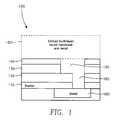
- FIG. 1is a dual-damascene stack for an all-in-one etching process.
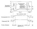
- FIG. 2 plot Aillustrates uncompensated transitions between process steps for plasma chamber conductance normalized to steady state.
- FIG. 2 plot Billustrates compensated transitions between process steps for plasma chamber conductance normalized to steady state.
- FIG. 2 plot Cillustrates a process variable with uncompensated ramp up and ramp down transitions.
- FIG. 2 plot Dillustrates a process variable with compensated ramp up and ramp down transitions.
- FIG. 2 plot Eillustrates a timing diagram with a compensated process chemistry.
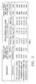
- FIG. 3is a table showing plasma-induced charging damage results for single and multi-step processes before and after compensation.
- FIG. 4Ais a graphical representation showing a conceptual charge damage risk as a function of source power-to-bias power ratio for compensated and uncompensated processes.
- FIG. 4Bis a graphical representation showing a conceptual charge damage risk as a function of source power-to-bias power ratio showing the effects of lower and higher pressure.
- Plasma-induced charging effectsare strong functions of chamber design and process conditions. During plasma-based processing of sensitive integrated circuits, there are multiple opportunities for these devices to become damaged. The focus on reducing charge damage has been during steady-state processing steps. For example, during etching or CVD processing, plasma-induced charging damage can occur during the steady-state processing step when process parameters are essentially fixed. Damage can also occur, however, in the non-steady state periods when process parameters are changing.
- the problem of plasma-induced charging damage associated with non-steady state periodsexists at lower source power frequencies, as well as high frequency plasma source power.
- High frequency plasma source poweris desirable as it is capable of providing denser plasma than low frequency plasma source power, which can facilitate high aspect ratio processing and reduces processing times.
- plasma-induced charging damageis more of a concern as gate oxides get thinner and device dimensions are getting smaller.
- the following teachingsare not limited to a specific plasma reactor, frequency, or process type, but are generally applicable in reducing charging damage and stabilization of plasma in all types of plasma processing, including deposition as well as etching.
- plasma uniformity and stabilitywere studied in a very-high-frequency capacitively coupled dielectric-etch chamber which may be used for all-in-one processing of sub-65 nm dual-damascene structures.
- Empirical resultsindicate that excessive magnetic-field strength and step-to-step transitions are the major variables influencing charging effects.
- Plasma stabilitycan be compensated by controlling these process parameters, and unstable and/or uncommon plasma states may also be avoided.
- Unstable and/or uncommon plasma statescan result from many anomalies such as software-control or hardware malfunctions. They may also occur when parasitic or secondary plasmas form, which impact and affect the primary plasma used to process the workpiece. The parasitic or secondary plasmas can cause unexpected etch-rate distribution deviations, e.g., uneven etching across the surface of the workpiece, or changes in the etch rate. Unstable plasma states can be controlled with step-to-step transitions to inhibit deviations from the expected etch-rate distribution (mean etch rate and uniformity). Thus, it is possible to inhibit etch-rate distribution that deviates from the otherwise expected etch-rate distribution.
- the risk of plasma charging damage during via 185 or trench 195 etchdepends on the integration scheme used in forming the dual-damascene structure. Shown in FIG. 1 is an all-in-one etch sequence of a more than seven layer dual-damascene structure suitable for the sub-65 nm node.
- the layers 110 - 150(layer 150 shown in phantom is an etched hardmask and resist multi-layer) are a combination of resist, hardmask, dielectric material, and barrier layers.
- the trench and via stepshave the highest risk of plasma-induced charging damage because of via-bottom metal 180 exposure.
- This sequencewas developed in a very-high-frequency capacitively coupled dielectric etcher and employs multiple steps with different source and bias power combinations to effectively etch diverse materials comprising the multiple layers 110 - 150 of the dual-damascene stack 100 .
- via and trench stepshave the highest risk of plasma-induced charging damage because of via-bottom metal 180 exposure.
- plasma instability during transitions from one plasma condition to anotheris a risk factor.
- Multiple process parametersare usually changed between steps in the etch sequence, including bias power, source power, pressure, magnetic field (which in some reactor types may be controlled with a charge species tuning unit or CSTU), and chemistry.
- bias powerwhich in some reactor types may be controlled with a charge species tuning unit or CSTU
- magnetic fieldwhich in some reactor types may be controlled with a charge species tuning unit or CSTU
- chemistrywhich in some reactor types may be controlled with a charge species tuning unit or CSTU
- CSTUcharge species tuning unit
- plot Bshows transitions that were compensated to produce more stable plasma during transitions.
- plot Bconductance excursions have been substantially reduced, and conductance at the beginning and after the etch Step 2 no longer deviates significantly from the steady-state conductance in Step 2 .
- FIG. 2shows that with the plasma conductance normalized with the steady-state conductance of a single-step process, the uncompensated transitions of plot A are marked by large excursions, while the compensated transitions of plot B are generally smoother with smaller excursions. These changes indicate that the compensated plasma is more stable while transitioning from one plasma state to another.
- FIG. 3shows that experimental data corroborate the reduction in damage risk when compensated transitions are used.
- the extent to which risk is reduced in a single-step etch processis show in Table 1 of FIG. 3 .
- uncompensated transitionsresult in 32% and 79% leakage-current yields for 200:1 and 100,000:1 antenna ratios, respectively. These yields improve to 97% and 99.5% with compensated transitions.
- EEPROM-based sensor results for the single-step etchshow similar improvements, as shown in Table 1.
- Mean and 95%-confidence-interval positive voltages and currentsdrop below the EEPROM-based thresholds.
- external-source gate-breakdown voltagesmeet the 100% yield criterion when compensated transitions are used. With uncompensated transitions, the yields for 1,000:1 and 100,000:1 antenna ratios are 88% and 37%, respectively, both of which are unacceptable.
- EEPROM-based sensorsresults, evaluated with the uncompensated multi-step sequence, reveal a very large damage risk as indicated by large voltage and current responses, shown in Table 1 of FIG. 5 .
- compensated transitions incorporated into the same sequenceEEPROM-based sensor voltages and currents are reduced to acceptable levels.
- the 200 mm antenna MOS capacitor gate-breakdown voltagesmeet the 100% yield criterion. Based on these data, plasma instabilities and the risk of plasma-induced charging effects can be minimized by compensating transitions between consecutive plasma-etching steps.
- a high risk factor that contributes to plasma-induced-charging sensitivitycan be compensated to reduce plasma charging damage.
- the plasma instability that can occur during transitions from one plasma state to anothercan be compensated.
- the plasmais more stable, and charging effects can be reduced.
- continuous etch processescan be developed, such as etching and ashing of complex multi-layer stacks, without plasma-charging-damage issues. This capability makes possible all-in-one via and trench etching, which is desirable for dual-damascene processes.
- plasma-induced charging damagemay be controlled and the recommended process operation window significantly increased.
- process parametersthat may be utilized to reduce plasma damage and/or avoid unstable plasma states.
- process power and power ratioBy controlling the process power and power ratio; the process pressure; the process chemistry; the magnetic field strength; and the transition ramp starting points, rates, and rate shapes for the above mentioned parameters, charging damage and/or deviations from expected etch-rate distributions can be reduced.
- charging damagethe following applies to reducing parasitic plasma and unexpected etch-rate distribution deviations cause therefrom.
- FIG. 4Ais a graphical representation showing a conceptual charge damage risk as a function of source power-to-bias power ratio. Charging damage risks are encountered in a source-frequency-based process without bias power. It has been determined that using a source-only plasma increases the risk since the sheath thickness is thinner and likely less stable, as indicated at the right side of FIG. 4A . As a result, the damage risk is higher since unusually large voltage and current gradients may develop at some point during the process. When the sheath thickness is increased with low bias frequency, charging damage reduction is observed, demonstrating that the wafer damage is influenced by the sheath. Thus, to reduce charging damage, a low source/bias power ratio W s /W b is desirable, for example within a range below approximately 1, with some minimum amount of bias power applied.
- the low-frequency poweris set within a threshold range to maintain sufficient sheath for high frequency source powered processes without increasing the damage risk.
- This low-frequency poweris dependent on plasma density and reactor type, but typically would be on the order of 100 W in an ENABLER reactor, available from Applied Materials, Inc., Santa Clara, Calif., which has an etching tool capable of operating at high frequencies greater than 100 MHz source power.
- the damage riskis in general, smaller, especially with the magnetic field, since the risk is higher with higher bias powers and magnetic fields.
- the damage-free windowincreases with equivalent magnetic-field strengths.
- a magnetic fieldis used during source-frequency based processing in order to redistribute the charged species such as the etchant radicals.
- the etch rate across the waferbecomes increasingly uniform.
- the magnetic field controlis a powerful uniformity-tuning knob. A consequence of using large magnetic fields is an increase in the damage risk since the voltage and current distributions are often negatively impacted when excessive field is employed.
- FIG. 4Bis a graphical representation showing a conceptual charge damage risk as a function of source power-to-bias power ratio showing the effects of lower and higher pressure.
- the pressureis increased, there is lower risk of damage during transitions as indicated by the dashed Higher Pressure line.
- the higher pressurestabilizes the plasma impedance and minimizes the damage risk, as compared to process transitions without pressure compensation.
- increasing pressure prior to transitioning the other parametersreduces the risk of charging damage occurring between process steps.
- the pressureis decreased, the risk of charging damage is increased as compared to process transitions without pressure compensation, as indicated by the Lower Pressure line.
- Another way to reduce charging damageis to control the process ramp starting points, rates, and rate shapes for process parameters such as source power, bias power, magnetic field strength, and pressure.
- the plasma-induced charging damageis sensitive to the transition from one process state to another. This sensitivity is also dependent on the approach to the next processing condition. There are a number of possibilities for each variable and an even larger number when the variables are changed at the same time. For example, the current approach is to simultaneously perform a linear ramp over a period of order one second from one processing step to another for each variable that requires a change, as illustrated in FIG. 2 , plot C of the Uncompensated VAR at 210 or 215 . These variables include low frequency bias power, high frequency source power, and magnetic field strength.
- Additional evidencesupports the delay of changing one or more parameters so that the plasma has time to react to these multiple changes.
- Thisis to ramp the power while maintaining a high pressure and, for example, an argon environment. Then, the non-reactive gas is replaced by the process gas, followed by a drop (or increase) in pressure to the final processing pressure.
- Source-frequency based processesare often used to remove organic films and typically do not use sputtering-type gases such as, but not limited to, argon.
- the organic-removing gassuch as oxygen is flowing inside the etcher prior to and after high source power is applied and removed, respectively. It has been determined, however, that during the source power ramp up to and ramp down from the steady-state high power, it is desirable to have a non-reactive gas such as argon in the etcher. It is during this period of time which is typically of order one second that other process variables are also changing from one state to another.
- etcher residence times of order one to three secondsare required in order to substantially change the etchant gas concentration. This time must include the time for the neutral gas to travel from the valve at the gas panel to the reactor chamber. By using this gas flushing step, monitoring wafers have reported a lower damage risk.
- the process chemistrymay include the introduction of Ar, or other non-reactive gas, for about 3-5 seconds to ensure that the Ar has been introduced to the plasma chamber to dilute the etchant gas concentration prior to process variable transition.
- Ar gasis flowed several seconds prior to ramp up 210 or 220 of a process variable to account for resident time for the Ar to travel from the gas panel and into the chamber. This ensures that Ar dilutes the reactive gas prior to transition of the process variable(s).
- Ar gasis flowed for several seconds prior to ramp down 215 or 225 , of a process variable.
- gas typemay be changed back to reactive gas prior to the end of the transition 210 , 215 , 220 , or 225 so long as sufficient resident Ar gas is delivered to, or remains in the chamber beyond the transition 210 , 215 , 220 , or 225 .
- the non-reactive gasmay be used as the non-reactive gas
- other diluent gasesmay be used.
- the non-reactive gasneed not be an inert gas, in this context, but instead can be a gas that dilutes the reactive gas and limits the change of the conductance (or impedance) of the plasma during a transition.
- the cusp configurationhas a substantially reduced the level of damage as compared to the mirror configuration.
- the damage riskis proportional to axial field strength.
- the use of source power with a large source-to-bias power ratioincreases the damage-free window size which may be further increased if the axial field strength is reduced.
- plasma-induced charging damagemay be controlled and the recommended process operation window significantly increased.
- the process chemistryis controlled during step transitions by introducing alternative chemistries that minimize the damage risk and instantaneous plasma non-uniformities.
- the process pressuremay be controlled during transition steps and step transitions by increasing pressure, which stabilizes the plasma impedance and minimizes the damage risk.
- the process powermay be controlled during transition steps such as between plasma processing steps, during the plasma formation (plasma strike), and during the dechucking step (plasma quenching) by maintaining a minimum low frequency bias power level (of order 100 W), which maintains a sufficient plasma sheath thickness and minimizes the damage risk.
- a minimum low frequency bias power levelof order 100 W
- the B-field strength (magnitude) and direction of the magnetic B-fieldmay be controlled during transition steps and step transitions in order to minimize the damage risk from magnetic-field-induced voltage and current gradients and fluctuations.
- the process ramp starting points, rates, and rate shapes for the above mentioned parametersmay be controlled since optimized values stabilize the plasma and minimize the damage risk.
- the power ratio of the multiple RF power sources operating at typical low and high fixed frequenciesmay be controlled since the damage risk is minimized with particular power ratios.
- the conductance, or impedance, of the plasmais used as a surrogate, to determine if charging damage is likely to occur during a transition.
- the plasma parameters, discussed herein,may be compensated so that the reactance, i.e. the impedance/conductance of the plasma does not contain excursions greater than some threshold value.
- the threshold for the acceptable excursion values of the plasma impedance/conductance from its steady state valuewill be dependent on the chamber, the process type, and the process parameters.
- the impedance/conductance of the plasmamay be monitored during the steady state and compared to the impedance/conductance of the plasma during the transition to develop a compensation scheme for a specific process.
- a maximum deviation of the impedance/conductance in some implementationsmay be a percentage value, while in others it may be an absolute value. For example, if the impedance/conductance increases more than approximately 200% of its steady value, additional compensation would be provided. Conversely, if the impedance/conductance value decreases by 50%, compensation in the form of increased bias, for example, could be provided to limit such an impedance/conductance excursion.
- a threshold range value for the impedance/conductancemay be used in determining whether charging damage is likely to occur.
- the acceptable excursion percentagewill vary based on process type, process parameters, chamber type, and device structures and tolerances. Therefore, the proper type and amount of compensation may be determined based on impedance/conductance measurements. Furthermore, transitions may be limited based on plasma impedance/conductance measurements.
- spectroscopy and/or plasma voltage/current measurementsmay be used as a surrogate to determine whether charging damage is likely to occur.
- impedance/conductance, spectroscopye.g. optical, endpoint technologies, etc.
- voltage/currente.g. voltage/current
- one or more of the measured surrogate characteristicsare monitored during steady state processing and during a process transition.
- the change of one or more of the surrogate characteristics through the process transitionis limited to inhibit charging damage, and/or to avoid unexpected etch-rate distribution deviations caused by parasitic or secondary plasmas. (It should be noted that charge damage is not always caused by unstable plasma, and, unstable plasma can cause unexpected etch-rate distribution deviations without causing damage).
- the implementations disclosed hereinare not limited to two frequencies, i.e. lower frequency bias power and higher frequency source power. Three or more frequencies may be used in some implementations. Moreover, certain implementations may use other than RF frequency, for example microwave, infrared, or x-ray. Furthermore, some or all of the various compensation implementations and approaches disclosed herein may be combined to further reduce the risk of charging damage.
Landscapes
- Engineering & Computer Science (AREA)
- Computer Hardware Design (AREA)
- Physics & Mathematics (AREA)
- Condensed Matter Physics & Semiconductors (AREA)
- General Physics & Mathematics (AREA)
- Manufacturing & Machinery (AREA)
- Chemical & Material Sciences (AREA)
- Microelectronics & Electronic Packaging (AREA)
- Power Engineering (AREA)
- General Chemical & Material Sciences (AREA)
- Inorganic Chemistry (AREA)
- Chemical Kinetics & Catalysis (AREA)
- Drying Of Semiconductors (AREA)
Abstract
Description
This application claims the benefit of U.S. Provisional Application No. 60/660,662, filed on Mar. 11, 2005, by Kutney, et. al., entitled METHOD TO REDUCE PLASMA-INDUCED CHARGING DAMAGE, herein incorporated by reference in its entirety.
This application is a continuation-in-part of U.S. application Ser. No. 11/366,301, by Kutney et. al., filed Mar. 1, 2006, assigned to the present assignee, hereby incorporated by reference, which claims the benefit of the above referenced Provisional Application 60/660,662, and which is a continuation-in-part of the following U.S. Applications assigned to the present assignee, which are hereby incorporated by reference:
U.S. application Ser. No. 11/046,656, filed Jan. 28, 2005 entitled PLASMA REACTOR WITH MINIMAL D.C. COILS FOR CUSP, SOLENOID AND MIRROR FIELDS FOR PLASMA UNIFORMITY AND DEVICE DAMAGE REDUCTION, by Daniel Hoffman et al., which is a continuation-in-part of Ser. No. 10/841,116, filed May 7, 2004 entitled CAPACITIVELY COUPLED PLASMA REACTOR WITH MAGNETIC PLASMA CONTROL by Daniel Hoffman, et al., which is divisional of U.S. application Ser. No. 10/192,271, filed Jul. 9, 2002 entitled CAPACITIVELY COUPLED PLASMA REACTOR WITH MAGNETIC PLASMA CONTROL by Daniel Hoffman, et al., all of which are assigned to the present assignee; and
U.S. application Ser. No. 11/046,538, filed Jan. 28, 2005 entitled PLASMA REACTOR OVERHEAD SOURCE POWER ELECTRODE WITH LOW ARCING TENDENCY, CYLINDRICAL GAS OUTLETS AND SHAPED SURFACE, by Douglas Buchberger et al., which is a continuation-in-part of U.S. application Ser. No. 10/754,280, filed Jan. 8, 2004 entitled PLASMA REACTOR WITH OVERHEAD RF SOURCE POWER ELECTRODE WITH LOW LOSS, LOW ARCING TENDENCY AND LOW CONTAMINATION by Daniel J. Hoffman et al., which is a continuation-in-part of U.S. patent application Ser. No. 10/028,922, filed Dec. 19, 2001 entitled PLASMA REACTOR WITH OVERHEAD RF ELECTRODE TUNED TO THE PLASMA by Daniel Hoffman et al., which is a continuation-in-part of U.S. patent application Ser. No. 09/527,342, filed Mar. 17, 2000 entitled PLASMA REACTOR WITH OVERHEAD RF ELECTRODE TUNED TO THE PLASMA by Daniel Hoffman et al., now issued as U.S. Pat. No. 6,528,751.
As structures fabricated on semiconductor wafers are reduced in size, charging damage associated with plasma processing becomes a serious problem. Charging damage generally occurs when structures being formed on the wafer with a plasma process, cause non-uniform charging of the structures. The non-uniform charging causes a differential voltage to form on the structures. Such a differential voltage can produce high currents or arcing in the structure that damage the structures. This can reduce yields and consequently increase manufacturing costs. As such, a need exists to provide methods capable of reducing plasma-induced charging damage during wafer processing.
In some implementations, a method is provided in a plasma processing chamber for stabilizing etch-rate distributions during a process transition from one process step to another process step. The method includes performing a pre-transition compensation of at least one other process parameter so as to avoid unstable plasma states by inhibiting formation of a parasitic plasma during the process transition. In certain implementations, performing the pre-transition compensation includes increasing a chamber pressure prior to the process transition. In certain implementations, performing the pre-transition compensation includes changing a gas chemistry in the chamber to a non-reactive gas chemistry prior to the process transition. In certain implementations, performing the pre-transition compensation includes setting a source power-to-bias power ratio within a range below about 1 for the transition. In certain implementations, performing the pre-transition compensation includes reducing a magnetic field strength prior to the process transition. In certain implementations, performing the pre-transition compensation includes initiating application of a bias power on the workpiece prior to the process transition.
In some implementations, a method is provided for processing a workpiece in plasma processing chamber which includes inhibiting deviations from an expected etch-rate distribution by avoiding unstable plasma states during a process transition from one process step to another process step. This may include changing at least one process parameter with a smooth non-linear transition. In certain implementations, changing the process parameter includes gradually changing from a first steady state to a transition state and gradually changing from the transition state to a second steady state. In certain implementations, changing of the process parameter is along a Boltzmann curve, or a Sigmoidal Richards curve. In certain implementations, changing of the process parameter includes changing at least one of a plasma source power, a bias power, a gas flow, a chamber pressure, or a magnetic field strength.
In some implementations, a method is provided for avoiding unstable plasma states in a plasma processing chamber during a process transition from one process step to another process step, the method includes sequentially changing selected process parameters such that a plasma is able to stabilize after each change prior to changing a next selected process parameter. In certain implementations, changing the plurality of process parameters includes providing a non-reactive gas chemistry in the chamber prior to changing other process parameters. In certain implementations, changing the plurality of process parameters includes changing the source power after increasing a chamber pressure. In certain implementations, changing the plurality of process parameters includes changing a source power after providing a non-reactive gas chemistry in the plasma processing chamber. In certain implementations, changing the plurality of process parameters includes changing a source power after initiating application of a bias power on the workpiece.
Plasma-induced charging effects are strong functions of chamber design and process conditions. During plasma-based processing of sensitive integrated circuits, there are multiple opportunities for these devices to become damaged. The focus on reducing charge damage has been during steady-state processing steps. For example, during etching or CVD processing, plasma-induced charging damage can occur during the steady-state processing step when process parameters are essentially fixed. Damage can also occur, however, in the non-steady state periods when process parameters are changing.
The problem of plasma-induced charging damage associated with non-steady state periods exists at lower source power frequencies, as well as high frequency plasma source power. High frequency plasma source power is desirable as it is capable of providing denser plasma than low frequency plasma source power, which can facilitate high aspect ratio processing and reduces processing times. Furthermore, plasma-induced charging damage is more of a concern as gate oxides get thinner and device dimensions are getting smaller. The following teachings, however, are not limited to a specific plasma reactor, frequency, or process type, but are generally applicable in reducing charging damage and stabilization of plasma in all types of plasma processing, including deposition as well as etching.
In this example, plasma uniformity and stability were studied in a very-high-frequency capacitively coupled dielectric-etch chamber which may be used for all-in-one processing of sub-65 nm dual-damascene structures. Empirical results indicate that excessive magnetic-field strength and step-to-step transitions are the major variables influencing charging effects. Plasma stability can be compensated by controlling these process parameters, and unstable and/or uncommon plasma states may also be avoided.
Unstable and/or uncommon plasma states can result from many anomalies such as software-control or hardware malfunctions. They may also occur when parasitic or secondary plasmas form, which impact and affect the primary plasma used to process the workpiece. The parasitic or secondary plasmas can cause unexpected etch-rate distribution deviations, e.g., uneven etching across the surface of the workpiece, or changes in the etch rate. Unstable plasma states can be controlled with step-to-step transitions to inhibit deviations from the expected etch-rate distribution (mean etch rate and uniformity). Thus, it is possible to inhibit etch-rate distribution that deviates from the otherwise expected etch-rate distribution.
During dual-damascene etching, device structures are sensitive to plasma-induced charging damage that could result in costly device-yield loss. This risk is high when metal lines are exposed through electrically transparent films or directly to the process plasma during key steps of the manufacturing sequence-low-κ dielectric etch, resist strip, and barrier removal-because charge imbalances can build up or instantaneously exceed the safe charging limit for a device during any one of these steps.
The risk of plasma charging damage during via185 ortrench 195 etch depends on the integration scheme used in forming the dual-damascene structure. Shown inFIG. 1 is an all-in-one etch sequence of a more than seven layer dual-damascene structure suitable for the sub-65 nm node. The layers110-150 (layer 150 shown in phantom is an etched hardmask and resist multi-layer) are a combination of resist, hardmask, dielectric material, and barrier layers. During the continuous multi-step etching of a dual-damascene stack with more than seven layers for the formation oftrench 195 and via185 structures, the trench and via steps have the highest risk of plasma-induced charging damage because of via-bottom metal 180 exposure. This sequence was developed in a very-high-frequency capacitively coupled dielectric etcher and employs multiple steps with different source and bias power combinations to effectively etch diverse materials comprising the multiple layers110-150 of the dual-damascene stack 100.
During the etching of the multi-layer dual-damascene stack 100 for bothtrench 195 and via185 structure formation with multiple steps, via and trench steps have the highest risk of plasma-induced charging damage because of via-bottom metal 180 exposure.
Turning toFIG. 2 , plasma instability during transitions from one plasma condition to another is a risk factor. Multiple process parameters are usually changed between steps in the etch sequence, including bias power, source power, pressure, magnetic field (which in some reactor types may be controlled with a charge species tuning unit or CSTU), and chemistry. During transitions between any two steps, adjusted process parameters are ramped to new setpoints in a simple linear fashion, as shown at210 or215 of plot C, or without any control whatsoever. In addition, these process parameters are simultaneously changed at the beginning of each step, often giving rise to situations in which multiple parameters are significantly changing before settling to their step set points.
Empirical data have revealed that uncompensated transitions increase the risk of plasma-induced charging damage and increase the existence of unstable and uncommon plasma states, because the plasma undergoes significant distribution, density, and energy changes. This uncompensated change can be represented by plasma conductance, which characterizes the energy allowed to flow through the plasma. As shown inFIG. 2 , plot A, for typical uncompensated transitions, conductance varies significantly in magnitude over time during transitions to and from the steady-state etching condition, shown inStep 2. In addition, the conductance at the beginning and afterStep 2 clearly deviates from the steady-state etch-step value. All of the indicators suggest that the plasma is undergoing significant change during transitions.
InFIG. 2 , plot B shows transitions that were compensated to produce more stable plasma during transitions. As shown inFIG. 2 , plot B, conductance excursions have been substantially reduced, and conductance at the beginning and after theetch Step 2 no longer deviates significantly from the steady-state conductance inStep 2. These improvements result from careful control and sequencing of process parameters, discussed further below, that are undergoing change and which may be implemented universally throughout the etch, or any other plasma processing sequence.
Thus,FIG. 2 shows that with the plasma conductance normalized with the steady-state conductance of a single-step process, the uncompensated transitions of plot A are marked by large excursions, while the compensated transitions of plot B are generally smoother with smaller excursions. These changes indicate that the compensated plasma is more stable while transitioning from one plasma state to another.
To verify the robustness of the transient-compensation solution, a multi-step sequence for etching a complex multi-layer dual-damascene stack was tested using EEPROM-based sensors. EEPROM-based sensors results, evaluated with the uncompensated multi-step sequence, reveal a very large damage risk as indicated by large voltage and current responses, shown in Table 1 ofFIG. 5 . With compensated transitions incorporated into the same sequence, EEPROM-based sensor voltages and currents are reduced to acceptable levels. In addition, the 200 mm antenna MOS capacitor gate-breakdown voltages meet the 100% yield criterion. Based on these data, plasma instabilities and the risk of plasma-induced charging effects can be minimized by compensating transitions between consecutive plasma-etching steps.
Thus, in the context of dual-damascene process, a high risk factor that contributes to plasma-induced-charging sensitivity can be compensated to reduce plasma charging damage. The plasma instability that can occur during transitions from one plasma state to another can be compensated. By continuously controlling the plasma state during a transition, the plasma is more stable, and charging effects can be reduced. With this risk factor mitigated, continuous etch processes can be developed, such as etching and ashing of complex multi-layer stacks, without plasma-charging-damage issues. This capability makes possible all-in-one via and trench etching, which is desirable for dual-damascene processes.
Further, carefully controlling process parameters and, hence the plasma state during transitions between multiple processing steps, and by introducing and controlling steady-state transition steps, plasma-induced charging damage may be controlled and the recommended process operation window significantly increased.
Discussed further below are process parameters that may be utilized to reduce plasma damage and/or avoid unstable plasma states. By controlling the process power and power ratio; the process pressure; the process chemistry; the magnetic field strength; and the transition ramp starting points, rates, and rate shapes for the above mentioned parameters, charging damage and/or deviations from expected etch-rate distributions can be reduced. Although the below discussion is discussed with reference to charging damage, the following applies to reducing parasitic plasma and unexpected etch-rate distribution deviations cause therefrom.
A way to reduce charging damage is to ensure that the power ratio between source power and bias power is within a low damage-risk regime.FIG. 4A is a graphical representation showing a conceptual charge damage risk as a function of source power-to-bias power ratio. Charging damage risks are encountered in a source-frequency-based process without bias power. It has been determined that using a source-only plasma increases the risk since the sheath thickness is thinner and likely less stable, as indicated at the right side ofFIG. 4A . As a result, the damage risk is higher since unusually large voltage and current gradients may develop at some point during the process. When the sheath thickness is increased with low bias frequency, charging damage reduction is observed, demonstrating that the wafer damage is influenced by the sheath. Thus, to reduce charging damage, a low source/bias power ratio Ws/Wbis desirable, for example within a range below approximately 1, with some minimum amount of bias power applied.
The low-frequency power is set within a threshold range to maintain sufficient sheath for high frequency source powered processes without increasing the damage risk. This low-frequency power is dependent on plasma density and reactor type, but typically would be on the order of 100 W in an ENABLER reactor, available from Applied Materials, Inc., Santa Clara, Calif., which has an etching tool capable of operating at high frequencies greater than 100 MHz source power.
Related to this is the success in minimizing damage when the power ratio is controlled and maximized. When the source-to-bias power ratio is small, the damage risk is in general, smaller, especially with the magnetic field, since the risk is higher with higher bias powers and magnetic fields. On the other hand, as more source power is applied, the damage-free window increases with equivalent magnetic-field strengths.
Thus, to reduce charging damage, source power only processes should be avoided and some amount of lower frequency bias power applied. In addition, this is true even for plasma strike, plasma quench, and dechucking. Damage risk has been observed by the present inventors to be lower during any process when low frequency bias power is applied during the usually high-frequency-only process.
Often, a magnetic field is used during source-frequency based processing in order to redistribute the charged species such as the etchant radicals. When sufficient magnetic field is used, the etch rate across the wafer becomes increasingly uniform. Thus, the magnetic field control is a powerful uniformity-tuning knob. A consequence of using large magnetic fields is an increase in the damage risk since the voltage and current distributions are often negatively impacted when excessive field is employed.
An additional factor in reducing charge damage is to control the process stability during transition steps by increasing pressure.FIG. 4B is a graphical representation showing a conceptual charge damage risk as a function of source power-to-bias power ratio showing the effects of lower and higher pressure. As shown inFIG. 4B , if the pressure is increased, there is lower risk of damage during transitions as indicated by the dashed Higher Pressure line. The higher pressure stabilizes the plasma impedance and minimizes the damage risk, as compared to process transitions without pressure compensation. Thus, increasing pressure prior to transitioning the other parameters reduces the risk of charging damage occurring between process steps. Conversely, if the pressure is decreased, the risk of charging damage is increased as compared to process transitions without pressure compensation, as indicated by the Lower Pressure line.
Another way to reduce charging damage is to control the process ramp starting points, rates, and rate shapes for process parameters such as source power, bias power, magnetic field strength, and pressure. The plasma-induced charging damage is sensitive to the transition from one process state to another. This sensitivity is also dependent on the approach to the next processing condition. There are a number of possibilities for each variable and an even larger number when the variables are changed at the same time. For example, the current approach is to simultaneously perform a linear ramp over a period of order one second from one processing step to another for each variable that requires a change, as illustrated inFIG. 2 , plot C of the Uncompensated VAR at210 or215. These variables include low frequency bias power, high frequency source power, and magnetic field strength. Other variables, however, such as pressure, temperature, gas flows, and backside helium pressures are several variables are programmed to reach their next set point as quickly as possible (infinite ramp rates). In the past, power and magnetic field strength ramp rates were fixed at approximately 1,000 W/s and 10 A/s, respectively.
To inhibit charging damage, however, power and magnetic field strength ramp rates, as well as the other parameters, should not be instantaneously large or extremely small. Furthermore, the plasma is more stable during transitions when ramp rates are smooth, e.g., without an instantaneous in slope, such as if they simulate a Boltzmann curve or a Sigmoidal Richards curve. A Boltzmann curve for example may be represented as:
where
- A1is the initial value,
- A2is the final value,
- x0is the center point, and
- dx is the time constant for the slope of the curve at x0
- A Boltzmann curve is illustrated in
FIG. 3 , plot D of the Compensated VAR at220 or225, in the transition betweenprocess Step 1 andStep 2 and betweenprocess Step 2 andStep 3, respectively. Transitions of this nature allow the plasma impedance to respond smoothly without shocking the plasma.
Additional evidence supports the delay of changing one or more parameters so that the plasma has time to react to these multiple changes. One example of this is to ramp the power while maintaining a high pressure and, for example, an argon environment. Then, the non-reactive gas is replaced by the process gas, followed by a drop (or increase) in pressure to the final processing pressure.
A way to reduce charging damage is to control the process chemistry during transitions by introducing alternative chemistries that minimize the damage risk. Source-frequency based processes are often used to remove organic films and typically do not use sputtering-type gases such as, but not limited to, argon. In some applications, the organic-removing gas such as oxygen is flowing inside the etcher prior to and after high source power is applied and removed, respectively. It has been determined, however, that during the source power ramp up to and ramp down from the steady-state high power, it is desirable to have a non-reactive gas such as argon in the etcher. It is during this period of time which is typically of order one second that other process variables are also changing from one state to another. Once variables reach their final processing state, then the chemistry can be safely switched with respect to plasma-induced-charging damage. Likewise, before the steady-state processing condition is ramped to next state (not necessarily ramped down), argon, or other non-reactive gas, is needed in the etcher in order to reduce the concentrations of the reactive process gas.
Typically, etcher residence times of order one to three seconds are required in order to substantially change the etchant gas concentration. This time must include the time for the neutral gas to travel from the valve at the gas panel to the reactor chamber. By using this gas flushing step, monitoring wafers have reported a lower damage risk.
As shown inFIG. 2 plot E, the process chemistry may include the introduction of Ar, or other non-reactive gas, for about 3-5 seconds to ensure that the Ar has been introduced to the plasma chamber to dilute the etchant gas concentration prior to process variable transition. Thus, Ar gas is flowed several seconds prior to ramp up210 or220 of a process variable to account for resident time for the Ar to travel from the gas panel and into the chamber. This ensures that Ar dilutes the reactive gas prior to transition of the process variable(s). Similarly, Ar gas is flowed for several seconds prior to ramp down215 or225, of a process variable. Although Ar flow is indicated beyond ramp up210 or220 and ramp down215 or225, gas type may be changed back to reactive gas prior to the end of thetransition transition
In one particular implementation, it has been observed that if the source power-to-bias power ratio Ws/Wbis greater than about 1, introducing Ar prior to a transition greatly reduces the risk of charge damage. Further, it is anticipated that other compensation means could be employed instead of, or in addition to, non-reactive gas introduction to significantly reduce the risk of charging damage when the source/bias power ratio Ws/Wbis above about 1.
As indicated above, although inert gases may be used as the non-reactive gas, in other implementations other diluent gases may be used. For example, it is anticipated that in some processes, nitrogen, or the like, may be used. Thus, the non-reactive gas need not be an inert gas, in this context, but instead can be a gas that dilutes the reactive gas and limits the change of the conductance (or impedance) of the plasma during a transition.
Yet another way to reduce charging damage is to control the B-field strength (magnitude) and direction of the B-field during transitions in order to minimize the damage risk from magnetic-field-induced voltage and current gradients and fluctuations. Investigations have also been performed with several magnetic-field configurations which alter the radial Brand axial Bzcomponents of the magnetic field across the wafer surface. When the radial component is zero along the entire wafer surface, the magnetic field is in its mirror configuration since only axial fields will exist along the wafer surface. The other extreme is the cusp configuration when the axial field is zero, while the radial component is nonzero. An example of a cusp configured reactor is disclosed in U.S. Pat. No. 5,674,321, by Pu and Shan, issued Oct. 7, 1997, entitled METHOD AND APPARATUS FOR PRODUCING PLASMA UNIFORMITY IN A MAGNETIC FIELD-ENHANCED PLASMA REACTOR, assigned to Applied Materials, Inc., Santa Clara, Calif., herein incorporated by reference in its entirety.
The cusp configuration has a substantially reduced the level of damage as compared to the mirror configuration. Thus, the damage risk is proportional to axial field strength. As mentioned previously, the use of source power with a large source-to-bias power ratio increases the damage-free window size which may be further increased if the axial field strength is reduced.
The approaches disclosed herein, however, which are used to minimize the damage risk, will also affect the semiconductor material in the etcher. These approaches may also provide benefit to the process which is to ultimately alter the material in a controlled fashion. Certain materials are sensitive to process parameters and by slowing, speeding, offsetting, and/or changing the approach midstream to the final state, the material will be affected.
Nevertheless, by carefully controlling process parameters and, hence the plasma state during transitions between multiple processing steps and by introducing and controlling steady-state transition steps, plasma-induced charging damage may be controlled and the recommended process operation window significantly increased. In order to achieve this reduction, the process chemistry is controlled during step transitions by introducing alternative chemistries that minimize the damage risk and instantaneous plasma non-uniformities. Alternatively, or in addition, the process pressure may be controlled during transition steps and step transitions by increasing pressure, which stabilizes the plasma impedance and minimizes the damage risk. Further, the process power may be controlled during transition steps such as between plasma processing steps, during the plasma formation (plasma strike), and during the dechucking step (plasma quenching) by maintaining a minimum low frequency bias power level (of order 100 W), which maintains a sufficient plasma sheath thickness and minimizes the damage risk. Moreover, the B-field strength (magnitude) and direction of the magnetic B-field may be controlled during transition steps and step transitions in order to minimize the damage risk from magnetic-field-induced voltage and current gradients and fluctuations. Furthermore, the process ramp starting points, rates, and rate shapes for the above mentioned parameters may be controlled since optimized values stabilize the plasma and minimize the damage risk. The power ratio of the multiple RF power sources operating at typical low and high fixed frequencies may be controlled since the damage risk is minimized with particular power ratios.
Referring toFIG. 2 , plots A & B, in some implementations, the conductance, or impedance, of the plasma is used as a surrogate, to determine if charging damage is likely to occur during a transition. The plasma parameters, discussed herein, may be compensated so that the reactance, i.e. the impedance/conductance of the plasma does not contain excursions greater than some threshold value. The threshold for the acceptable excursion values of the plasma impedance/conductance from its steady state value (either pre-transition or post transition steady state value), will be dependent on the chamber, the process type, and the process parameters.
As such, the impedance/conductance of the plasma may be monitored during the steady state and compared to the impedance/conductance of the plasma during the transition to develop a compensation scheme for a specific process. A maximum deviation of the impedance/conductance in some implementations may be a percentage value, while in others it may be an absolute value. For example, if the impedance/conductance increases more than approximately 200% of its steady value, additional compensation would be provided. Conversely, if the impedance/conductance value decreases by 50%, compensation in the form of increased bias, for example, could be provided to limit such an impedance/conductance excursion. Similarly, a threshold range value for the impedance/conductance may be used in determining whether charging damage is likely to occur. The acceptable excursion percentage will vary based on process type, process parameters, chamber type, and device structures and tolerances. Therefore, the proper type and amount of compensation may be determined based on impedance/conductance measurements. Furthermore, transitions may be limited based on plasma impedance/conductance measurements.
Similarly, other methodologies such as spectroscopy and/or plasma voltage/current measurements, alone or in combination with impedance/conductance measurements, may be used as a surrogate to determine whether charging damage is likely to occur. Further, it also is possible to use the above methodologies, impedance/conductance, spectroscopy (e.g. optical, endpoint technologies, etc.), or voltage/current, or combinations thereof, to inhibit deviations from the expected etch-rate distribution resulting from parasitic or secondary plasma.
As such, one or more of the measured surrogate characteristics are monitored during steady state processing and during a process transition. The change of one or more of the surrogate characteristics through the process transition is limited to inhibit charging damage, and/or to avoid unexpected etch-rate distribution deviations caused by parasitic or secondary plasmas. (It should be noted that charge damage is not always caused by unstable plasma, and, unstable plasma can cause unexpected etch-rate distribution deviations without causing damage).
The implementations disclosed herein are not limited to two frequencies, i.e. lower frequency bias power and higher frequency source power. Three or more frequencies may be used in some implementations. Moreover, certain implementations may use other than RF frequency, for example microwave, infrared, or x-ray. Furthermore, some or all of the various compensation implementations and approaches disclosed herein may be combined to further reduce the risk of charging damage.
While the invention herein disclosed has been described by the specific embodiments and implementations, numerous modifications and variations could be made thereto by those skilled in the art without departing from the scope of the invention set forth in the claims.
Claims (13)
1. A method of etching in a plasma processing chamber comprising:
conducting a process transition from one process step to another process step, wherein the process transition comprises changing of at least one process parameter; and
performing a pre-transition compensation of at least one other process parameter so as to avoid unstable plasma states by inhibiting formation of a parasitic plasma during the process transition.
2. The method ofclaim 1 wherein performing the pre-transition compensation comprises increasing a sheath size above a workpiece being processed by initiating application of a bias power prior to the process transition.
3. The method ofclaim 1 wherein performing a pre-transition compensation comprises increasing a chamber pressure prior to the process transition.
4. The method ofclaim 3 further comprising reducing the chamber pressure for processing after the process transition.
5. The method ofclaim 3 wherein performing the pre-transition compensation comprises increasing a chamber pressure prior to the process transition if a source power-to-bias power ratio is greater than about 1.
6. The method ofclaim 3 wherein performing the pre-transition compensation comprises setting a source power-to-bias power ratio within a range below about 1 for the transition.
7. The method ofclaim 3 wherein performing the pre-transition compensation comprises initiating a bias power prior to the process transition.
8. The method ofclaim 7 wherein initiating the bias power comprises setting bias power to about 100 W prior to the process transition.
9. The method ofclaim 1 wherein performing the pre-transition compensation comprises changing a gas chemistry in the chamber to a non-reactive gas prior to the process transition.
10. The method ofclaim 9 further introducing a reactive gas after the process transition for processing a workpiece.
11. The method ofclaim 9 wherein performing the pre-transition compensation comprises changing a gas chemistry in the chamber to a non-reactive gas prior to the process transition if a source power-to-bias power ratio is greater than about 1.
12. The method ofclaim 9 wherein introducing the non-reactive gas into the plasma processing chamber prior to the process transition comprises starting a flow of the non-reactive gas to the process chamber before the process transition at a time prior to the process transition greater than a residence time of the non-reactive gas to arrive from a gas panel to the processing chamber.
13. The method ofclaim 12 wherein introducing the non-reactive gas into the plasma processing chamber comprises introducing argon at least 2 seconds prior to the process transition.
Priority Applications (2)
| Application Number | Priority Date | Filing Date | Title |
|---|---|---|---|
| US11/372,752US8048806B2 (en) | 2000-03-17 | 2006-03-10 | Methods to avoid unstable plasma states during a process transition |
| TW96108462ATWI389178B (en) | 2006-03-10 | 2007-03-12 | Methods to avoid unstable plasma states during a process transition |
Applications Claiming Priority (10)
| Application Number | Priority Date | Filing Date | Title |
|---|---|---|---|
| US09/527,342US6528751B1 (en) | 2000-03-17 | 2000-03-17 | Plasma reactor with overhead RF electrode tuned to the plasma |
| US10/028,922US7030335B2 (en) | 2000-03-17 | 2001-12-19 | Plasma reactor with overhead RF electrode tuned to the plasma with arcing suppression |
| US10/192,271US6853141B2 (en) | 2002-05-22 | 2002-07-09 | Capacitively coupled plasma reactor with magnetic plasma control |
| US10/754,280US7220937B2 (en) | 2000-03-17 | 2004-01-08 | Plasma reactor with overhead RF source power electrode with low loss, low arcing tendency and low contamination |
| US10/841,116US20050001556A1 (en) | 2002-07-09 | 2004-05-07 | Capacitively coupled plasma reactor with magnetic plasma control |
| US11/046,538US7196283B2 (en) | 2000-03-17 | 2005-01-28 | Plasma reactor overhead source power electrode with low arcing tendency, cylindrical gas outlets and shaped surface |
| US11/046,656US8617351B2 (en) | 2002-07-09 | 2005-01-28 | Plasma reactor with minimal D.C. coils for cusp, solenoid and mirror fields for plasma uniformity and device damage reduction |
| US66066205P | 2005-03-11 | 2005-03-11 | |
| US11/366,301US20070048882A1 (en) | 2000-03-17 | 2006-03-01 | Method to reduce plasma-induced charging damage |
| US11/372,752US8048806B2 (en) | 2000-03-17 | 2006-03-10 | Methods to avoid unstable plasma states during a process transition |
Related Parent Applications (1)
| Application Number | Title | Priority Date | Filing Date |
|---|---|---|---|
| US11/366,301Continuation-In-PartUS20070048882A1 (en) | 2000-03-17 | 2006-03-01 | Method to reduce plasma-induced charging damage |
Publications (2)
| Publication Number | Publication Date |
|---|---|
| US20070066064A1 US20070066064A1 (en) | 2007-03-22 |
| US8048806B2true US8048806B2 (en) | 2011-11-01 |
Family
ID=37884744
Family Applications (1)
| Application Number | Title | Priority Date | Filing Date |
|---|---|---|---|
| US11/372,752Expired - Fee RelatedUS8048806B2 (en) | 2000-03-17 | 2006-03-10 | Methods to avoid unstable plasma states during a process transition |
Country Status (1)
| Country | Link |
|---|---|
| US (1) | US8048806B2 (en) |
Cited By (2)
| Publication number | Priority date | Publication date | Assignee | Title |
|---|---|---|---|---|
| US10009028B2 (en) | 2016-09-30 | 2018-06-26 | Lam Research Corporation | Frequency and match tuning in one state and frequency tuning in the other state |
| US10068926B2 (en) | 2011-05-05 | 2018-09-04 | Semiconductor Energy Laboratory Co., Ltd. | Semiconductor device and method for manufacturing the same |
Families Citing this family (7)
| Publication number | Priority date | Publication date | Assignee | Title |
|---|---|---|---|---|
| US7883633B2 (en) | 2003-02-14 | 2011-02-08 | Applied Materials, Inc. | Method for shaping a magnetic field in a magnetic field-enhanced plasma reactor |
| US8048328B2 (en) | 2003-02-14 | 2011-11-01 | Applied Materials, Inc. | Method for shaping a magnetic field in a magnetic field-enhanced plasma reactor |
| JP4145925B2 (en)* | 2006-01-31 | 2008-09-03 | シャープ株式会社 | Plasma etching method |
| US20110060442A1 (en)* | 2009-09-10 | 2011-03-10 | Valcore Jr John C | Methods and arrangement for detecting a wafer-released event within a plasma processing chamber |
| US8797705B2 (en)* | 2009-09-10 | 2014-08-05 | Lam Research Corporation | Methods and arrangement for plasma dechuck optimization based on coupling of plasma signaling to substrate position and potential |
| JP6408903B2 (en)* | 2014-12-25 | 2018-10-17 | 東京エレクトロン株式会社 | Etching processing method and etching processing apparatus |
| CN111270224B (en)* | 2018-12-04 | 2022-06-28 | 财团法人金属工业研究发展中心 | Chemical vapor deposition apparatus, method for the same, and power compensation module |
Citations (260)
| Publication number | Priority date | Publication date | Assignee | Title |
|---|---|---|---|---|
| US2951960A (en) | 1959-03-24 | 1960-09-06 | Tung Sol Electric Inc | Gaseous discharge device |
| US2967926A (en) | 1958-03-10 | 1961-01-10 | Union Carbide Corp | Testing process and apparatus |
| US3355615A (en) | 1964-04-27 | 1967-11-28 | Bihan Raymond Le | Ion source having critically dimensioned extraction means |
| US3610986A (en) | 1970-05-01 | 1971-10-05 | Union Carbide Corp | Electron beam source including a pilot nonthermionic, electron source |
| US4293794A (en) | 1980-04-01 | 1981-10-06 | Kapetanakos Christos A | Generation of intense, high-energy ion pulses by magnetic compression of ion rings |
| US4401054A (en) | 1980-05-02 | 1983-08-30 | Nippon Telegraph & Telephone Public Corporation | Plasma deposition apparatus |
| US4438368A (en) | 1980-11-05 | 1984-03-20 | Mitsubishi Denki Kabushiki Kaisha | Plasma treating apparatus |
| US4458180A (en) | 1982-02-18 | 1984-07-03 | Elscint Ltd. | Plasma electron source for cold-cathode discharge device or the like |
| US4464223A (en) | 1983-10-03 | 1984-08-07 | Tegal Corp. | Plasma reactor apparatus and method |
| US4526643A (en) | 1983-03-24 | 1985-07-02 | Tokyo Shibaura Denki Kabushiki Kaisha | Dry etching apparatus using reactive ions |
| US4552639A (en) | 1984-07-20 | 1985-11-12 | Varian Associates, Inc. | Magnetron sputter etching system |
| US4570106A (en) | 1982-02-18 | 1986-02-11 | Elscint, Inc. | Plasma electron source for cold-cathode discharge device or the like |
| US4579618A (en) | 1984-01-06 | 1986-04-01 | Tegal Corporation | Plasma reactor apparatus |
| US4600492A (en) | 1984-07-25 | 1986-07-15 | Kabushiki Kaisha Tokuda Seisakusho | Magnet driving method and device for same |
| US4631106A (en) | 1984-09-19 | 1986-12-23 | Hitachi, Ltd. | Plasma processor |
| US4665489A (en) | 1984-03-15 | 1987-05-12 | Kabushiki Kaisha Meidensha | Unmanned vehicle control system and method |
| US4665487A (en) | 1984-05-25 | 1987-05-12 | Kabushiki Kaisha Meidensha | Unmanned vehicle control system and method |
| US4668365A (en) | 1984-10-25 | 1987-05-26 | Applied Materials, Inc. | Apparatus and method for magnetron-enhanced plasma-assisted chemical vapor deposition |
| US4668338A (en) | 1985-12-30 | 1987-05-26 | Applied Materials, Inc. | Magnetron-enhanced plasma etching process |
| US4740268A (en) | 1987-05-04 | 1988-04-26 | Motorola Inc. | Magnetically enhanced plasma system |
| US4792378A (en) | 1987-12-15 | 1988-12-20 | Texas Instruments Incorporated | Gas dispersion disk for use in plasma enhanced chemical vapor deposition reactor |
| US4829215A (en) | 1984-08-31 | 1989-05-09 | Anelva Corporation | Discharge reaction apparatus utilizing dynamic magnetic field |
| US4842683A (en) | 1986-12-19 | 1989-06-27 | Applied Materials, Inc. | Magnetic field-enhanced plasma etch reactor |
| US4859908A (en) | 1986-09-24 | 1989-08-22 | Matsushita Electric Industrial Co., Ltd. | Plasma processing apparatus for large area ion irradiation |
| US4888518A (en) | 1987-11-16 | 1989-12-19 | Itt Corporation | Gas circulation apparatus for ceramic electron tubes |
| US4947085A (en) | 1987-03-27 | 1990-08-07 | Mitsubishi Denki Kabushiki Kaisha | Plasma processor |
| US4950956A (en) | 1986-10-08 | 1990-08-21 | Anelva Corporation | Plasma processing apparatus |
| US4963242A (en) | 1988-05-23 | 1990-10-16 | Nippon Telegraph And Telephone Corporation | Plasma etching apparatus |
| US4973883A (en) | 1987-05-01 | 1990-11-27 | Semiconductor Energy Laborator Co., Ltd. | Plasma processing apparatus with a lisitano coil |
| US4990229A (en) | 1989-06-13 | 1991-02-05 | Plasma & Materials Technologies, Inc. | High density plasma deposition and etching apparatus |
| US5006760A (en) | 1987-01-09 | 1991-04-09 | Motorola, Inc. | Capacitive feed for plasma reactor |
| US5017835A (en) | 1987-03-18 | 1991-05-21 | Hans Oechsner | High-frequency ion source |
| US5032202A (en) | 1989-10-03 | 1991-07-16 | Martin Marietta Energy Systems, Inc. | Plasma generating apparatus for large area plasma processing |
| US5053678A (en) | 1988-03-16 | 1991-10-01 | Hitachi, Ltd. | Microwave ion source |
| US5055853A (en) | 1988-10-03 | 1991-10-08 | Garnier Robert C | Magnetic frill generator |
| US5061838A (en) | 1989-06-23 | 1991-10-29 | Massachusetts Institute Of Technology | Toroidal electron cyclotron resonance reactor |
| US5074456A (en) | 1990-09-18 | 1991-12-24 | Lam Research Corporation | Composite electrode for plasma processes |
| US5077499A (en) | 1990-04-18 | 1991-12-31 | Mitsubishi Denki Kabushiki Kaisha | High-frequency feeding method for use in plasma apparatus and device for carrying out the method |
| US5079481A (en) | 1990-08-02 | 1992-01-07 | Texas Instruments Incorporated | Plasma-assisted processing magneton with magnetic field adjustment |
| US5081398A (en) | 1989-10-20 | 1992-01-14 | Board Of Trustees Operating Michigan State University | Resonant radio frequency wave coupler apparatus using higher modes |
| US5087857A (en) | 1990-06-18 | 1992-02-11 | Samsung Electronics Co., Ltd. | Plasma generating apparatus and method using modulation system |
| US5089083A (en) | 1989-04-25 | 1992-02-18 | Tokyo Electron Limited | Plasma etching method |
| US5107170A (en) | 1988-10-18 | 1992-04-21 | Nissin Electric Co., Ltd. | Ion source having auxillary ion chamber |
| US5115167A (en) | 1988-04-05 | 1992-05-19 | Mitsubishi Denki Kabushiki Kaisha | Plasma processor |
| US5120466A (en) | 1984-07-13 | 1992-06-09 | Canon Kabushiki Kaisha | Fluid crystal device |
| US5122251A (en) | 1989-06-13 | 1992-06-16 | Plasma & Materials Technologies, Inc. | High density plasma deposition and etching apparatus |
| US5140223A (en) | 1989-07-18 | 1992-08-18 | Leybold Aktiengesellschaft | Circuit for adjusting the impedance of a plasma section to a high-frequency generator |
| US5145554A (en)* | 1989-02-23 | 1992-09-08 | Seiko Epson Corporation | Method of anisotropic dry etching of thin film semiconductors |
| US5175472A (en) | 1991-12-30 | 1992-12-29 | Comdel, Inc. | Power monitor of RF plasma |
| US5195045A (en) | 1991-02-27 | 1993-03-16 | Astec America, Inc. | Automatic impedance matching apparatus and method |
| US5198725A (en) | 1991-07-12 | 1993-03-30 | Lam Research Corporation | Method of producing flat ecr layer in microwave plasma device and apparatus therefor |
| US5208512A (en) | 1990-10-16 | 1993-05-04 | International Business Machines Corporation | Scanned electron cyclotron resonance plasma source |
| US5210466A (en) | 1989-10-03 | 1993-05-11 | Applied Materials, Inc. | VHF/UHF reactor system |
| US5211825A (en) | 1990-09-21 | 1993-05-18 | Hitachi, Ltd. | Plasma processing apparatus and the method of the same |
| US5213658A (en) | 1990-10-26 | 1993-05-25 | Mitsubishi Denki Kabushiki Kaisha | Plasma processing method |
| US5215619A (en) | 1986-12-19 | 1993-06-01 | Applied Materials, Inc. | Magnetic field-enhanced plasma etch reactor |
| US5218271A (en) | 1990-06-22 | 1993-06-08 | Research Institute Of Applied Mechanics And Electrodynamics Of Moscow Aviation Institute | Plasma accelerator with closed electron drift |
| US5223457A (en) | 1989-10-03 | 1993-06-29 | Applied Materials, Inc. | High-frequency semiconductor wafer processing method using a negative self-bias |
| US5225024A (en) | 1989-05-08 | 1993-07-06 | Applied Materials, Inc. | Magnetically enhanced plasma reactor system for semiconductor processing |
| US5246532A (en) | 1990-10-26 | 1993-09-21 | Mitsubishi Denki Kabushiki Kaisha | Plasma processing apparatus |
| US5252194A (en) | 1990-01-26 | 1993-10-12 | Varian Associates, Inc. | Rotating sputtering apparatus for selected erosion |
| US5256931A (en) | 1990-10-12 | 1993-10-26 | U.S. Philips Corp. | Electron source having a material-retaining device |
| US5272417A (en) | 1989-05-12 | 1993-12-21 | Tadahiro Ohmi | Device for plasma process |
| US5273610A (en) | 1992-06-23 | 1993-12-28 | Association Institutions For Material Sciences, Inc. | Apparatus and method for determining power in plasma processing |
| US5274306A (en) | 1990-08-31 | 1993-12-28 | Kaufman & Robinson, Inc. | Capacitively coupled radiofrequency plasma source |
| US5279669A (en) | 1991-12-13 | 1994-01-18 | International Business Machines Corporation | Plasma reactor for processing substrates comprising means for inducing electron cyclotron resonance (ECR) and ion cyclotron resonance (ICR) conditions |
| US5280219A (en) | 1991-05-21 | 1994-01-18 | Materials Research Corporation | Cluster tool soft etch module and ECR plasma generator therefor |
| US5300460A (en) | 1989-10-03 | 1994-04-05 | Applied Materials, Inc. | UHF/VHF plasma for use in forming integrated circuit structures on semiconductor wafers |
| US5304279A (en) | 1990-08-10 | 1994-04-19 | International Business Machines Corporation | Radio frequency induction/multipole plasma processing tool |
| US5308417A (en) | 1991-09-12 | 1994-05-03 | Applied Materials, Inc. | Uniformity for magnetically enhanced plasma chambers |
| US5312778A (en) | 1989-10-03 | 1994-05-17 | Applied Materials, Inc. | Method for plasma processing using magnetically enhanced plasma chemical vapor deposition |
| US5314603A (en) | 1991-07-24 | 1994-05-24 | Tokyo Electron Yamanashi Limited | Plasma processing apparatus capable of detecting and regulating actual RF power at electrode within chamber |
| US5325019A (en) | 1992-08-21 | 1994-06-28 | Sematech, Inc. | Control of plasma process by use of harmonic frequency components of voltage and current |
| US5345145A (en) | 1992-03-31 | 1994-09-06 | Matsushita Electric Industrial Co., Ltd. | Method and apparatus for generating highly dense uniform plasma in a high frequency electric field |
| US5401351A (en) | 1993-01-27 | 1995-03-28 | Nec Corporation | Radio frequency electron cyclotron resonance plasma etching apparatus |
| US5432315A (en) | 1991-05-31 | 1995-07-11 | Hitachi, Ltd. | Plasma process apparatus including ground electrode with protection film |
| US5433836A (en) | 1991-03-25 | 1995-07-18 | Commonwealth Scientific And Industrial Research Organization | Arc source macroparticle filter |
| US5444207A (en) | 1992-03-26 | 1995-08-22 | Kabushiki Kaisha Toshiba | Plasma generating device and surface processing device and method for processing wafers in a uniform magnetic field |
| US5449977A (en) | 1992-04-17 | 1995-09-12 | Matsushita Electric Industrial Co., Ltd. | Apparatus and method for generating plasma of uniform flux density |
| EP0678903A1 (en) | 1994-04-20 | 1995-10-25 | Tokyo Electron Limited | Plasma treatment method and apparatus |
| US5463525A (en) | 1993-12-20 | 1995-10-31 | International Business Machines Corporation | Guard ring electrostatic chuck |
| US5467013A (en) | 1993-12-07 | 1995-11-14 | Sematech, Inc. | Radio frequency monitor for semiconductor process control |
| US5474648A (en) | 1994-07-29 | 1995-12-12 | Lsi Logic Corporation | Uniform and repeatable plasma processing |
| US5503676A (en) | 1994-09-19 | 1996-04-02 | Lam Research Corporation | Apparatus and method for magnetron in-situ cleaning of plasma reaction chamber |
| US5506475A (en) | 1994-03-22 | 1996-04-09 | Martin Marietta Energy Systems, Inc. | Microwave electron cyclotron electron resonance (ECR) ion source with a large, uniformly distributed, axially symmetric, ECR plasma volume |
| US5512130A (en) | 1994-03-09 | 1996-04-30 | Texas Instruments Incorporated | Method and apparatus of etching a clean trench in a semiconductor material |
| US5519373A (en) | 1993-12-28 | 1996-05-21 | Shin-Etsu Chemical Co., Ltd. | Dipole ring magnet for use in magnetron sputtering or magnetron etching |
| US5527394A (en) | 1991-06-08 | 1996-06-18 | Fraunhofer Gesellschaft Zur Forderung Der Angewandten Forschung E.V. | Apparatus for plasma enhanced processing of substrates |
| US5534070A (en) | 1993-03-31 | 1996-07-09 | Canon Kabushiki Kaisha | Plasma CVD process using a very-high-frequency and plasma CVD apparatus |
| US5534108A (en) | 1993-05-28 | 1996-07-09 | Applied Materials, Inc. | Method and apparatus for altering magnetic coil current to produce etch uniformity in a magnetic field-enhanced plasma reactor |
| US5537004A (en) | 1993-03-06 | 1996-07-16 | Tokyo Electron Limited | Low frequency electron cyclotron resonance plasma processor |
| US5554223A (en) | 1993-03-06 | 1996-09-10 | Tokyo Electron Limited | Plasma processing apparatus with a rotating electromagnetic field |
| US5556717A (en) | 1993-10-27 | 1996-09-17 | Sony Corporation | Coating-type magnetic recording medium comprising an ascorbic ester compound in or on a magnetic recording layer |
| US5556549A (en) | 1994-05-02 | 1996-09-17 | Lsi Logic Corporation | Power control and delivery in plasma processing equipment |
| US5565382A (en) | 1993-10-12 | 1996-10-15 | Applied Materials, Inc. | Process for forming tungsten silicide on semiconductor wafer using dichlorosilane gas |
| US5567268A (en) | 1994-01-31 | 1996-10-22 | Sony Corporation | Plasma processing apparatus and method for carrying out plasma processing by using such plasma processing apparatus |
| US5576629A (en) | 1994-10-24 | 1996-11-19 | Fourth State Technology, Inc. | Plasma monitoring and control method and system |
| US5576600A (en) | 1994-12-23 | 1996-11-19 | Dynatenn, Inc. | Broad high current ion source |
| US5587038A (en) | 1994-06-16 | 1996-12-24 | Princeton University | Apparatus and process for producing high density axially extending plasmas |
| US5592055A (en) | 1994-10-21 | 1997-01-07 | Proel Tecnologie S.P.A. | Radio-frequency plasma source |
| US5595627A (en) | 1995-02-07 | 1997-01-21 | Tokyo Electron Limited | Plasma etching method |
| US5605637A (en) | 1994-12-15 | 1997-02-25 | Applied Materials Inc. | Adjustable dc bias control in a plasma reactor |
| US5627435A (en) | 1993-07-12 | 1997-05-06 | The Boc Group, Inc. | Hollow cathode array and method of cleaning sheet stock therewith |
| US5659276A (en) | 1995-07-12 | 1997-08-19 | Shin-Etsu Chemical Co., Ltd. | Magnetic field generator for magnetron plasma |
| US5660671A (en) | 1990-09-29 | 1997-08-26 | Tokyo Electron Limited | Magnetron plasma processing apparatus and processing method |
| US5662770A (en) | 1993-04-16 | 1997-09-02 | Micron Technology, Inc. | Method and apparatus for improving etch uniformity in remote source plasma reactors with powered wafer chucks |
| US5662819A (en) | 1994-02-10 | 1997-09-02 | Sony Corporation | Plasma processing method with controlled ion/radical ratio |
| US5685914A (en) | 1994-04-05 | 1997-11-11 | Applied Materials, Inc. | Focus ring for semiconductor wafer processing in a plasma reactor |
| US5705019A (en) | 1994-10-26 | 1998-01-06 | Sumitomo Metal Industries, Ltd. | Plasma processing apparatus |
| US5707486A (en) | 1990-07-31 | 1998-01-13 | Applied Materials, Inc. | Plasma reactor using UHF/VHF and RF triode source, and process |
| US5710486A (en) | 1995-05-08 | 1998-01-20 | Applied Materials, Inc. | Inductively and multi-capacitively coupled plasma reactor |
| US5717294A (en) | 1994-02-28 | 1998-02-10 | Kabushiki Kaisha Toshiba | Plasma process apparatus |
| US5718795A (en) | 1995-08-21 | 1998-02-17 | Applied Materials, Inc. | Radial magnetic field enhancement for plasma processing |
| US5720826A (en) | 1995-05-30 | 1998-02-24 | Canon Kabushiki Kaisha | Photovoltaic element and fabrication process thereof |
| US5726412A (en) | 1993-02-18 | 1998-03-10 | Commissariat A L'energie Atomique | Linear microwave source for plasma surface treatment |
| US5733511A (en) | 1994-06-21 | 1998-03-31 | The Boc Group, Inc. | Power distribution for multiple electrode plasma systems using quarter wavelength transmission lines |
| US5759424A (en)* | 1994-03-24 | 1998-06-02 | Hitachi, Ltd. | Plasma processing apparatus and processing method |
| US5770922A (en) | 1996-07-22 | 1998-06-23 | Eni Technologies, Inc. | Baseband V-I probe |
| US5783102A (en) | 1996-02-05 | 1998-07-21 | International Business Machines Corporation | Negative ion deductive source for etching high aspect ratio structures |
| EP0719447B1 (en) | 1993-09-17 | 1998-07-22 | Isis Innovation Limited | Rf plasma reactor |
| US5792376A (en) | 1995-01-06 | 1998-08-11 | Kabushiki Kaisha Toshiba | Plasma processing apparatus and plasma processing method |
| US5798029A (en) | 1994-04-22 | 1998-08-25 | Applied Materials, Inc. | Target for sputtering equipment |
| US5824607A (en) | 1997-02-06 | 1998-10-20 | Applied Materials, Inc. | Plasma confinement for an inductively coupled plasma reactor |
| US5846885A (en) | 1995-08-23 | 1998-12-08 | Fujitsu Limited | Plasma treatment method |
| US5849372A (en) | 1993-09-17 | 1998-12-15 | Isis Innovation Limited | RF plasma reactor and methods of generating RF plasma |
| US5849136A (en) | 1991-10-11 | 1998-12-15 | Applied Materials, Inc. | High frequency semiconductor wafer processing apparatus and method |
| US5855685A (en) | 1995-10-09 | 1999-01-05 | Anelva Corporation | Plasma enhanced CVD apparatus, plasma enhanced processing apparatus and plasma enhanced CVD method |
| US5855725A (en) | 1995-05-30 | 1999-01-05 | Anelva Corporation | Vacuum processing system and method of removing film deposited on inner face of vacuum vessel in the vacuum processing system |
| US5858819A (en) | 1994-06-15 | 1999-01-12 | Seiko Epson Corporation | Fabrication method for a thin film semiconductor device, the thin film semiconductor device itself, liquid crystal display, and electronic device |
| US5863376A (en) | 1996-06-05 | 1999-01-26 | Lam Research Corporation | Temperature controlling method and apparatus for a plasma processing chamber |
| US5866986A (en) | 1996-08-05 | 1999-02-02 | Integrated Electronic Innovations, Inc. | Microwave gas phase plasma source |
| US5868848A (en) | 1995-06-07 | 1999-02-09 | Tokyo Electron Limited | Plasma processing apparatus |
| US5876576A (en) | 1997-10-27 | 1999-03-02 | Applied Materials, Inc. | Apparatus for sputtering magnetic target materials |
| US5880034A (en) | 1997-04-29 | 1999-03-09 | Princeton University | Reduction of semiconductor structure damage during reactive ion etching |
| US5885358A (en) | 1996-07-09 | 1999-03-23 | Applied Materials, Inc. | Gas injection slit nozzle for a plasma process reactor |
| US5902461A (en) | 1997-09-03 | 1999-05-11 | Applied Materials, Inc. | Apparatus and method for enhancing uniformity of a metal film formed on a substrate with the aid of an inductively coupled plasma |
| US5907220A (en) | 1996-03-13 | 1999-05-25 | Applied Materials, Inc. | Magnetron for low pressure full face erosion |
| US5914568A (en) | 1997-03-19 | 1999-06-22 | Tokyo Electron Limited | Plasma processing apparatus |
| US5929717A (en) | 1998-01-09 | 1999-07-27 | Lam Research Corporation | Method of and apparatus for minimizing plasma instability in an RF processor |
| US5936481A (en) | 1997-09-10 | 1999-08-10 | Adtec Corporation Limited | System for impedance matching and power control for apparatus for high frequency plasma treatment |
| US5942074A (en) | 1996-03-29 | 1999-08-24 | Lam Research Corporation | Single-piece gas director for plasma reactors |
| US5945008A (en) | 1994-09-29 | 1999-08-31 | Sony Corporation | Method and apparatus for plasma control |
| US5958140A (en) | 1995-07-27 | 1999-09-28 | Tokyo Electron Limited | One-by-one type heat-processing apparatus |
| US5971591A (en) | 1997-10-20 | 1999-10-26 | Eni Technologies, Inc. | Process detection system for plasma process |
| US5997962A (en) | 1995-06-30 | 1999-12-07 | Tokyo Electron Limited | Plasma process utilizing an electrostatic chuck |
| US6000360A (en) | 1996-07-03 | 1999-12-14 | Tokyo Electron Limited | Plasma processing apparatus |
| US6014943A (en) | 1996-09-12 | 2000-01-18 | Tokyo Electron Limited | Plasma process device |
| US6016131A (en) | 1995-08-16 | 2000-01-18 | Applied Materials, Inc. | Inductively coupled plasma reactor with an inductive coil antenna having independent loops |
| US6015476A (en) | 1998-02-05 | 2000-01-18 | Applied Materials, Inc. | Plasma reactor magnet with independently controllable parallel axial current-carrying elements |
| US6030486A (en) | 1996-01-24 | 2000-02-29 | Applied Materials, Inc. | Magnetically confined plasma reactor for processing a semiconductor wafer |
| US6043608A (en) | 1996-10-31 | 2000-03-28 | Nec Corporation | Plasma processing apparatus |
| US6051151A (en) | 1997-11-12 | 2000-04-18 | International Business Machines Corporation | Apparatus and method of producing a negative ion plasma |
| US6074518A (en)* | 1994-04-20 | 2000-06-13 | Tokyo Electron Limited | Plasma processing apparatus |
| US6073577A (en) | 1998-06-30 | 2000-06-13 | Lam Research Corporation | Electrode for plasma processes and method for manufacture and use thereof |
| US6076482A (en) | 1997-09-20 | 2000-06-20 | Applied Materials, Inc. | Thin film processing plasma reactor chamber with radially upward sloping ceiling for promoting radially outward diffusion |
| US6079356A (en) | 1997-12-02 | 2000-06-27 | Applied Materials, Inc. | Reactor optimized for chemical vapor deposition of titanium |
| US6085688A (en) | 1998-03-27 | 2000-07-11 | Applied Materials, Inc. | Method and apparatus for improving processing and reducing charge damage in an inductively coupled plasma reactor |
| US6089182A (en) | 1995-08-17 | 2000-07-18 | Tokyo Electron Limited | Plasma processing apparatus |
| US6093457A (en) | 1997-03-27 | 2000-07-25 | Matsushita Electric Industrial Co., Ltd. | Method for plasma processing |
| US6095084A (en) | 1996-02-02 | 2000-08-01 | Applied Materials, Inc. | High density plasma process chamber |
| US6106663A (en) | 1998-06-19 | 2000-08-22 | Lam Research Corporation | Semiconductor process chamber electrode |
| US6110395A (en) | 1997-08-26 | 2000-08-29 | Trikon Technologies, Inc. | Method and structure for controlling plasma uniformity |
| US6142096A (en) | 1996-05-16 | 2000-11-07 | Sharp Kabushiki Kaisha | Electronic device manufacturing apparatus and method for manufacturing electronic device |
| US6152071A (en) | 1996-12-11 | 2000-11-28 | Canon Kabushiki Kaisha | High-frequency introducing means, plasma treatment apparatus, and plasma treatment method |
| US6155200A (en) | 1997-07-08 | 2000-12-05 | Tokyo Electron Limited | ECR plasma generator and an ECR system using the generator |
| US6162709A (en) | 1997-12-01 | 2000-12-19 | Applied Materials, Inc. | Use of an asymmetric waveform to control ion bombardment during substrate processing |
| US6174450B1 (en) | 1997-04-16 | 2001-01-16 | Lam Research Corporation | Methods and apparatus for controlling ion energy and plasma density in a plasma processing system |
| US6188564B1 (en) | 1999-03-31 | 2001-02-13 | Lam Research Corporation | Method and apparatus for compensating non-uniform wafer processing in plasma processing chamber |
| US6190495B1 (en) | 1998-07-29 | 2001-02-20 | Tokyo Electron Limited | Magnetron plasma processing apparatus |
| US6213959B1 (en) | 1998-04-15 | 2001-04-10 | Clete Kushida | Morphometric modeling system and method |
| US6213050B1 (en) | 1998-12-01 | 2001-04-10 | Silicon Genesis Corporation | Enhanced plasma mode and computer system for plasma immersion ion implantation |
| US6218312B1 (en) | 1996-05-13 | 2001-04-17 | Applied Materials Inc. | Plasma reactor with heated source of a polymer-hardening precursor material |
| US6245190B1 (en) | 1997-03-26 | 2001-06-12 | Hitachi, Ltd. | Plasma processing system and plasma processing method |
| US6247242B1 (en) | 1998-03-19 | 2001-06-19 | Pioneer Electronic Corporation | Mechanism for detecting position of a movable member |
| US6251216B1 (en) | 1997-12-17 | 2001-06-26 | Matsushita Electronics Corporation | Apparatus and method for plasma processing |
| JP2001185542A (en) | 1999-12-27 | 2001-07-06 | Hitachi Ltd | Plasma processing apparatus and plasma processing method using the same |
| US6262538B1 (en) | 1999-08-26 | 2001-07-17 | International Business Machines Corporation | High density plasma tool with adjustable uniformity and stochastic electron heating for reduced gas cracking |
| US6274008B1 (en) | 2000-01-21 | 2001-08-14 | Applied Materials, Inc. | Integrated process for copper via filling |
| US6284673B2 (en) | 1999-07-08 | 2001-09-04 | Genus Inc. | Method for providing uniform gas delivery to substrates in CVD and PECVD processes |
| US6291999B1 (en) | 1997-09-30 | 2001-09-18 | Daihen Corp. | Plasma monitoring apparatus |
| US6294026B1 (en) | 1996-11-26 | 2001-09-25 | Siemens Aktiengesellschaft | Distribution plate for a reaction chamber with multiple gas inlets and separate mass flow control loops |
| US6296747B1 (en) | 2000-06-22 | 2001-10-02 | Applied Materials, Inc. | Baffled perforated shield in a plasma sputtering reactor |
| US6300227B1 (en) | 1998-12-01 | 2001-10-09 | Silicon Genesis Corporation | Enhanced plasma mode and system for plasma immersion ion implantation |
| JP2001319920A (en) | 2000-03-01 | 2001-11-16 | Hitachi Ltd | Plasma processing apparatus and processing method |
| US6337292B1 (en) | 1998-10-29 | 2002-01-08 | Lg. Philips Lcd Co., Ltd. | Method of forming silicon oxide layer and method of manufacturing thin film transistor thereby |
| US6346915B1 (en) | 1999-08-06 | 2002-02-12 | Matsushita Electric Industrial Co., Ltd. | Plasma processing method and apparatus |
| US6376388B1 (en) | 1993-07-16 | 2002-04-23 | Fujitsu Limited | Dry etching with reduced damage to MOS device |
| US6382129B1 (en) | 1998-03-24 | 2002-05-07 | Applied Materials, Inc. | Semiconductor wafer processor, plasma generating apparatus, magnetic field generator, and method of generating a magnetic field |
| US6392350B1 (en) | 1998-06-30 | 2002-05-21 | Tokyo Electron Limited | Plasma processing method |
| US6404088B1 (en) | 1999-09-07 | 2002-06-11 | Ebara Corporation | Magnetic bearing device |
| US6415736B1 (en) | 1999-06-30 | 2002-07-09 | Lam Research Corporation | Gas distribution apparatus for semiconductor processing |
| US20020092618A1 (en) | 1992-12-01 | 2002-07-18 | Applied Materials, Inc. | Parallel-plate electrode plasma reactor having an inductive antenna coupling power through a parallel plate electrode |
| TW497173B (en) | 2000-04-06 | 2002-08-01 | Applied Materials Inc | Inductively coupled plasma source with controllable power deposition |
| US6432259B1 (en) | 1999-12-14 | 2002-08-13 | Applied Materials, Inc. | Plasma reactor cooled ceiling with an array of thermally isolated plasma heated mini-gas distribution plates |
| US6431297B1 (en) | 1999-02-18 | 2002-08-13 | Kabushiki Kaisha Toshiba | Apparatus for driving electric car by inverter-controlled motor through gear mechanism |
| US20020108933A1 (en) | 2000-03-17 | 2002-08-15 | Applied Materials, Inc. | Plasma reactor with overhead RF electrode tuned to the plasma with arcing suppression |
| US6436388B2 (en) | 1997-03-15 | 2002-08-20 | Ikue Kudo | Method of treating rhabdomyolysis by administering hepatocyte growth factor |
| US6436230B1 (en) | 1999-11-26 | 2002-08-20 | Tokyo Electron Limited | Process device |
| US6444104B2 (en) | 2000-01-21 | 2002-09-03 | Applied Materials, Inc. | Sputtering target having an annular vault |
| US6444039B1 (en) | 2000-03-07 | 2002-09-03 | Simplus Systems Corporation | Three-dimensional showerhead apparatus |
| US6449568B1 (en) | 1998-02-27 | 2002-09-10 | Eni Technology, Inc. | Voltage-current sensor with high matching directivity |
| US6451703B1 (en) | 2000-03-10 | 2002-09-17 | Applied Materials, Inc. | Magnetically enhanced plasma etch process using a heavy fluorocarbon etching gas |
| US20020139477A1 (en) | 2001-03-30 | 2002-10-03 | Lam Research Corporation | Plasma processing method and apparatus with control of plasma excitation power |
| US6462481B1 (en) | 2000-07-06 | 2002-10-08 | Applied Materials Inc. | Plasma reactor having a symmetric parallel conductor coil antenna |
| US6475335B1 (en) | 1995-02-15 | 2002-11-05 | Applied Materials, Inc. | RF plasma reactor with hybrid conductor and multi-radius dome ceiling |
| US6485617B2 (en) | 2000-01-21 | 2002-11-26 | Applied Materials, Inc. | Sputtering method utilizing an extended plasma region |
| US6488807B1 (en) | 1991-06-27 | 2002-12-03 | Applied Materials, Inc. | Magnetic confinement in a plasma reactor having an RF bias electrode |
| US20020179443A1 (en) | 2001-05-31 | 2002-12-05 | Satoshi Hada | Power supply control system for heater used in gas sensor |
| US6491801B1 (en) | 2001-08-07 | 2002-12-10 | Applied Materials, Inc. | Auxiliary vertical magnet outside a nested unbalanced magnetron |
| US6495009B1 (en) | 2001-08-07 | 2002-12-17 | Applied Materials, Inc. | Auxiliary in-plane magnet inside a nested unbalanced magnetron |
| US6506687B1 (en)* | 1998-06-24 | 2003-01-14 | Hitachi, Ltd. | Dry etching device and method of producing semiconductor devices |
| US6521082B1 (en) | 2002-04-16 | 2003-02-18 | Applied Materials Inc. | Magnetically enhanced plasma apparatus and method with enhanced plasma uniformity and enhanced ion energy control |
| US6528751B1 (en) | 2000-03-17 | 2003-03-04 | Applied Materials, Inc. | Plasma reactor with overhead RF electrode tuned to the plasma |
| US6545580B2 (en) | 1998-09-09 | 2003-04-08 | Veeco Instruments, Inc. | Electromagnetic field generator and method of operation |
| US20030085000A1 (en) | 2001-07-06 | 2003-05-08 | Applied Materials, Inc. | Method and apparatus for controlling the magnetic field intensity in a plasma enhanced semiconductor wafer processing chamber |
| US6579421B1 (en) | 1999-01-07 | 2003-06-17 | Applied Materials, Inc. | Transverse magnetic field for ionized sputter deposition |
| US6586886B1 (en) | 2001-12-19 | 2003-07-01 | Applied Materials, Inc. | Gas distribution plate electrode for a plasma reactor |
| US20030132195A1 (en) | 2000-09-12 | 2003-07-17 | Manabu Edamura | Plasma processing method and apparatus using dynamic sensing of a plasma environment |
| US6599399B2 (en) | 1997-03-07 | 2003-07-29 | Applied Materials, Inc. | Sputtering method to generate ionized metal plasma using electron beams and magnetic field |
| US6599367B1 (en) | 1998-03-06 | 2003-07-29 | Tokyo Electron Limited | Vacuum processing apparatus |
| US20030148040A1 (en)* | 2002-02-07 | 2003-08-07 | Hiroshi Satoh | Coating method and aperture plate |
| US6610184B2 (en) | 2001-11-14 | 2003-08-26 | Applied Materials, Inc. | Magnet array in conjunction with rotating magnetron for plasma sputtering |
| US20030168427A1 (en) | 1995-12-04 | 2003-09-11 | Daniel L. Flamm | Process depending on plasma discharges sustained by inductive coupling |
| US6627050B2 (en) | 2000-07-28 | 2003-09-30 | Applied Materials, Inc. | Method and apparatus for depositing a tantalum-containing layer on a substrate |
| US6639950B1 (en) | 1998-10-23 | 2003-10-28 | Nokia Networks Oy | Method and arrangement for correcting phase error in linearization loop of power amplifier |
| US6652712B2 (en) | 2001-12-19 | 2003-11-25 | Applied Materials, Inc | Inductive antenna for a plasma reactor producing reduced fluorine dissociation |
| US20030218427A1 (en) | 2002-05-22 | 2003-11-27 | Applied Materials, Inc. | Capacitively coupled plasma reactor with magnetic plasma control |
| US6663754B2 (en) | 2001-04-13 | 2003-12-16 | Applied Materials, Inc. | Tubular magnet as center pole in unbalanced sputtering magnetron |
| US6663715B1 (en) | 1999-11-10 | 2003-12-16 | Nec Corporation | Plasma CVD apparatus for large area CVD film |
| US6674241B2 (en) | 2001-07-24 | 2004-01-06 | Tokyo Electron Limited | Plasma processing apparatus and method of controlling chemistry |
| US6673199B1 (en) | 2001-03-07 | 2004-01-06 | Applied Materials, Inc. | Shaping a plasma with a magnetic field to control etch rate uniformity |
| US20040011467A1 (en) | 1999-11-15 | 2004-01-22 | Hemker David J. | Materials and gas chemistries for processing systems |
| US20040035365A1 (en)* | 2002-07-12 | 2004-02-26 | Yohei Yamazawa | Plasma processing apparatus |
| US6700376B2 (en) | 2001-02-02 | 2004-03-02 | Ge Medical Systems Global Technology Company, Llc | Method and apparatus for correcting static magnetic field using a pair of magnetic fields which are the same or different from each other in intensity and direction |
| US20040056602A1 (en) | 2002-07-09 | 2004-03-25 | Applied Materials, Inc. | Capacitively coupled plasma reactor with uniform radial distribution of plasma |
| US6716302B2 (en) | 2000-11-01 | 2004-04-06 | Applied Materials Inc. | Dielectric etch chamber with expanded process window |
| US6761804B2 (en) | 2002-02-11 | 2004-07-13 | Applied Materials, Inc. | Inverted magnetron |
| US20040134615A1 (en)* | 2002-10-23 | 2004-07-15 | Klaus Breitschwerdt | Device and method for anisotropic plasma etching of a substrate, particularly a silicon element |
| US20040134611A1 (en) | 2001-01-22 | 2004-07-15 | Tokyo Electron Limited | Plasma process system and plasma process method |
| US6764575B1 (en) | 1999-09-02 | 2004-07-20 | Tokyo Electron Limited | Magnetron plasma processing apparatus |
| US6767429B2 (en) | 2000-01-12 | 2004-07-27 | Tokyo Electron Limited | Vacuum processing apparatus |
| US20040182516A1 (en) | 2003-02-14 | 2004-09-23 | Applied Materials, Inc. | Method and apparatus for shaping a magnetic field in a magnetic field-enhanced plasma reactor |
| US6805770B1 (en) | 2001-08-30 | 2004-10-19 | Oster Magnetics, Inc. | Technique for improving uniformity of magnetic fields that rotate or oscillate about an axis |
| US6818097B2 (en) | 2002-04-22 | 2004-11-16 | Nisshinbo Industries, Inc. | Highly heat-resistant plasma etching electrode and dry etching device including the same |
| US20040233027A1 (en) | 2002-09-09 | 2004-11-25 | Oster Eugene L. | Apparatus for manipulating magnetic fields |
| US20050001556A1 (en) | 2002-07-09 | 2005-01-06 | Applied Materials, Inc. | Capacitively coupled plasma reactor with magnetic plasma control |
| US6872259B2 (en) | 2000-03-30 | 2005-03-29 | Tokyo Electron Limited | Method of and apparatus for tunable gas injection in a plasma processing system |
| US6894245B2 (en) | 2000-03-17 | 2005-05-17 | Applied Materials, Inc. | Merie plasma reactor with overhead RF electrode tuned to the plasma with arcing suppression |
| US20050126710A1 (en)* | 2002-03-05 | 2005-06-16 | Franz Laermer | Device and method for anisotropically plasma etching of a substrate, particularly a silicon body |
| US20050167051A1 (en) | 2002-07-09 | 2005-08-04 | Applied Materials, Inc. | Plasma reactor with minimal D.C. coils for cusp, solenoid and mirror fields for plasma uniformity and device damage reduction |
| US20050178748A1 (en)* | 2000-03-17 | 2005-08-18 | Applied Materials, Inc. | Plasma reactor overhead source power electrode with low arcing tendency, cylindrical gas outlets and shaped surface |
| US20060169410A1 (en)* | 2005-02-01 | 2006-08-03 | Kenji Maeda | Plasma processing apparatus capable of controlling plasma emission intensity |
| US20060175016A1 (en)* | 2005-02-07 | 2006-08-10 | Manabu Edamura | Plasma processing apparatus |
| US7141757B2 (en)* | 2000-03-17 | 2006-11-28 | Applied Materials, Inc. | Plasma reactor with overhead RF source power electrode having a resonance that is virtually pressure independent |
| US7163641B2 (en) | 1998-04-24 | 2007-01-16 | Micron Technology, Inc. | Method of forming high aspect ratio apertures |
| US7218503B2 (en) | 1998-09-30 | 2007-05-15 | Lam Research Corporation | Method of determining the correct average bias compensation voltage during a plasma process |
| US20070212811A1 (en)* | 2002-06-05 | 2007-09-13 | Applied Materials, Inc. | Low temperature CVD process with selected stress of the CVD layer on CMOS devices |
| US20080044960A1 (en)* | 2000-08-11 | 2008-02-21 | Applied Materials, Inc. | Semiconductor on insulator vertical transistor fabrication and doping process |
| US7458335B1 (en) | 2002-10-10 | 2008-12-02 | Applied Materials, Inc. | Uniform magnetically enhanced reactive ion etching using nested electromagnetic coils |
| JP4247878B2 (en) | 2002-12-16 | 2009-04-02 | 東海カーボン株式会社 | Carbon black pigment for black matrix |
Family Cites Families (2)
| Publication number | Priority date | Publication date | Assignee | Title |
|---|---|---|---|---|
| US3555615A (en)* | 1968-08-08 | 1971-01-19 | Usm Corp | Rotational moulding machines |
| US5198045A (en)* | 1991-05-14 | 1993-03-30 | Reynolds Metals Company | Low density high strength al-li alloy |
- 2006
- 2006-03-10USUS11/372,752patent/US8048806B2/ennot_activeExpired - Fee Related
Patent Citations (294)
| Publication number | Priority date | Publication date | Assignee | Title |
|---|---|---|---|---|
| US2967926A (en) | 1958-03-10 | 1961-01-10 | Union Carbide Corp | Testing process and apparatus |
| US2951960A (en) | 1959-03-24 | 1960-09-06 | Tung Sol Electric Inc | Gaseous discharge device |
| US3355615A (en) | 1964-04-27 | 1967-11-28 | Bihan Raymond Le | Ion source having critically dimensioned extraction means |
| US3610986A (en) | 1970-05-01 | 1971-10-05 | Union Carbide Corp | Electron beam source including a pilot nonthermionic, electron source |
| US4293794A (en) | 1980-04-01 | 1981-10-06 | Kapetanakos Christos A | Generation of intense, high-energy ion pulses by magnetic compression of ion rings |
| US4401054A (en) | 1980-05-02 | 1983-08-30 | Nippon Telegraph & Telephone Public Corporation | Plasma deposition apparatus |
| US4438368A (en) | 1980-11-05 | 1984-03-20 | Mitsubishi Denki Kabushiki Kaisha | Plasma treating apparatus |
| US4570106A (en) | 1982-02-18 | 1986-02-11 | Elscint, Inc. | Plasma electron source for cold-cathode discharge device or the like |
| US4458180A (en) | 1982-02-18 | 1984-07-03 | Elscint Ltd. | Plasma electron source for cold-cathode discharge device or the like |
| US4526643A (en) | 1983-03-24 | 1985-07-02 | Tokyo Shibaura Denki Kabushiki Kaisha | Dry etching apparatus using reactive ions |
| US4464223A (en) | 1983-10-03 | 1984-08-07 | Tegal Corp. | Plasma reactor apparatus and method |
| US4464223B1 (en) | 1983-10-03 | 1991-04-09 | Tegal Corp | |
| US4579618A (en) | 1984-01-06 | 1986-04-01 | Tegal Corporation | Plasma reactor apparatus |
| US4665489A (en) | 1984-03-15 | 1987-05-12 | Kabushiki Kaisha Meidensha | Unmanned vehicle control system and method |
| US4665487A (en) | 1984-05-25 | 1987-05-12 | Kabushiki Kaisha Meidensha | Unmanned vehicle control system and method |
| US5120466A (en) | 1984-07-13 | 1992-06-09 | Canon Kabushiki Kaisha | Fluid crystal device |
| US4552639A (en) | 1984-07-20 | 1985-11-12 | Varian Associates, Inc. | Magnetron sputter etching system |
| US4600492A (en) | 1984-07-25 | 1986-07-15 | Kabushiki Kaisha Tokuda Seisakusho | Magnet driving method and device for same |
| US4829215A (en) | 1984-08-31 | 1989-05-09 | Anelva Corporation | Discharge reaction apparatus utilizing dynamic magnetic field |
| US4631106A (en) | 1984-09-19 | 1986-12-23 | Hitachi, Ltd. | Plasma processor |
| US4668365A (en) | 1984-10-25 | 1987-05-26 | Applied Materials, Inc. | Apparatus and method for magnetron-enhanced plasma-assisted chemical vapor deposition |
| US4668338A (en) | 1985-12-30 | 1987-05-26 | Applied Materials, Inc. | Magnetron-enhanced plasma etching process |
| US4859908A (en) | 1986-09-24 | 1989-08-22 | Matsushita Electric Industrial Co., Ltd. | Plasma processing apparatus for large area ion irradiation |
| US4950956A (en) | 1986-10-08 | 1990-08-21 | Anelva Corporation | Plasma processing apparatus |
| US4842683A (en) | 1986-12-19 | 1989-06-27 | Applied Materials, Inc. | Magnetic field-enhanced plasma etch reactor |
| US5215619A (en) | 1986-12-19 | 1993-06-01 | Applied Materials, Inc. | Magnetic field-enhanced plasma etch reactor |
| US5006760A (en) | 1987-01-09 | 1991-04-09 | Motorola, Inc. | Capacitive feed for plasma reactor |
| US5017835A (en) | 1987-03-18 | 1991-05-21 | Hans Oechsner | High-frequency ion source |
| US4947085A (en) | 1987-03-27 | 1990-08-07 | Mitsubishi Denki Kabushiki Kaisha | Plasma processor |
| US4973883A (en) | 1987-05-01 | 1990-11-27 | Semiconductor Energy Laborator Co., Ltd. | Plasma processing apparatus with a lisitano coil |
| US4740268A (en) | 1987-05-04 | 1988-04-26 | Motorola Inc. | Magnetically enhanced plasma system |
| US4888518A (en) | 1987-11-16 | 1989-12-19 | Itt Corporation | Gas circulation apparatus for ceramic electron tubes |
| US4792378A (en) | 1987-12-15 | 1988-12-20 | Texas Instruments Incorporated | Gas dispersion disk for use in plasma enhanced chemical vapor deposition reactor |
| US5053678A (en) | 1988-03-16 | 1991-10-01 | Hitachi, Ltd. | Microwave ion source |
| US5115167A (en) | 1988-04-05 | 1992-05-19 | Mitsubishi Denki Kabushiki Kaisha | Plasma processor |
| US4963242A (en) | 1988-05-23 | 1990-10-16 | Nippon Telegraph And Telephone Corporation | Plasma etching apparatus |
| EP0343500B1 (en) | 1988-05-23 | 1994-01-19 | Nippon Telegraph And Telephone Corporation | Plasma etching apparatus |
| US5055853A (en) | 1988-10-03 | 1991-10-08 | Garnier Robert C | Magnetic frill generator |
| US5107170A (en) | 1988-10-18 | 1992-04-21 | Nissin Electric Co., Ltd. | Ion source having auxillary ion chamber |
| US5145554A (en)* | 1989-02-23 | 1992-09-08 | Seiko Epson Corporation | Method of anisotropic dry etching of thin film semiconductors |
| US5089083A (en) | 1989-04-25 | 1992-02-18 | Tokyo Electron Limited | Plasma etching method |
| US5225024A (en) | 1989-05-08 | 1993-07-06 | Applied Materials, Inc. | Magnetically enhanced plasma reactor system for semiconductor processing |
| US5272417A (en) | 1989-05-12 | 1993-12-21 | Tadahiro Ohmi | Device for plasma process |
| US4990229A (en) | 1989-06-13 | 1991-02-05 | Plasma & Materials Technologies, Inc. | High density plasma deposition and etching apparatus |
| US5122251A (en) | 1989-06-13 | 1992-06-16 | Plasma & Materials Technologies, Inc. | High density plasma deposition and etching apparatus |
| US5061838A (en) | 1989-06-23 | 1991-10-29 | Massachusetts Institute Of Technology | Toroidal electron cyclotron resonance reactor |
| US5140223A (en) | 1989-07-18 | 1992-08-18 | Leybold Aktiengesellschaft | Circuit for adjusting the impedance of a plasma section to a high-frequency generator |
| US5300460A (en) | 1989-10-03 | 1994-04-05 | Applied Materials, Inc. | UHF/VHF plasma for use in forming integrated circuit structures on semiconductor wafers |
| US5312778A (en) | 1989-10-03 | 1994-05-17 | Applied Materials, Inc. | Method for plasma processing using magnetically enhanced plasma chemical vapor deposition |
| US5618382A (en) | 1989-10-03 | 1997-04-08 | Applied Materials, Inc. | High-frequency semiconductor wafer processing apparatus and method |
| US5032202A (en) | 1989-10-03 | 1991-07-16 | Martin Marietta Energy Systems, Inc. | Plasma generating apparatus for large area plasma processing |
| US5223457A (en) | 1989-10-03 | 1993-06-29 | Applied Materials, Inc. | High-frequency semiconductor wafer processing method using a negative self-bias |
| US5210466A (en) | 1989-10-03 | 1993-05-11 | Applied Materials, Inc. | VHF/UHF reactor system |
| US5081398A (en) | 1989-10-20 | 1992-01-14 | Board Of Trustees Operating Michigan State University | Resonant radio frequency wave coupler apparatus using higher modes |
| US5252194A (en) | 1990-01-26 | 1993-10-12 | Varian Associates, Inc. | Rotating sputtering apparatus for selected erosion |
| US5077499A (en) | 1990-04-18 | 1991-12-31 | Mitsubishi Denki Kabushiki Kaisha | High-frequency feeding method for use in plasma apparatus and device for carrying out the method |
| US5087857A (en) | 1990-06-18 | 1992-02-11 | Samsung Electronics Co., Ltd. | Plasma generating apparatus and method using modulation system |
| US5218271A (en) | 1990-06-22 | 1993-06-08 | Research Institute Of Applied Mechanics And Electrodynamics Of Moscow Aviation Institute | Plasma accelerator with closed electron drift |
| US5707486A (en) | 1990-07-31 | 1998-01-13 | Applied Materials, Inc. | Plasma reactor using UHF/VHF and RF triode source, and process |
| US5079481A (en) | 1990-08-02 | 1992-01-07 | Texas Instruments Incorporated | Plasma-assisted processing magneton with magnetic field adjustment |
| US5304279A (en) | 1990-08-10 | 1994-04-19 | International Business Machines Corporation | Radio frequency induction/multipole plasma processing tool |
| US5274306A (en) | 1990-08-31 | 1993-12-28 | Kaufman & Robinson, Inc. | Capacitively coupled radiofrequency plasma source |
| US5074456A (en) | 1990-09-18 | 1991-12-24 | Lam Research Corporation | Composite electrode for plasma processes |
| US5211825A (en) | 1990-09-21 | 1993-05-18 | Hitachi, Ltd. | Plasma processing apparatus and the method of the same |
| US5660671A (en) | 1990-09-29 | 1997-08-26 | Tokyo Electron Limited | Magnetron plasma processing apparatus and processing method |
| US5256931A (en) | 1990-10-12 | 1993-10-26 | U.S. Philips Corp. | Electron source having a material-retaining device |
| US5208512A (en) | 1990-10-16 | 1993-05-04 | International Business Machines Corporation | Scanned electron cyclotron resonance plasma source |
| US5213658A (en) | 1990-10-26 | 1993-05-25 | Mitsubishi Denki Kabushiki Kaisha | Plasma processing method |
| US5246532A (en) | 1990-10-26 | 1993-09-21 | Mitsubishi Denki Kabushiki Kaisha | Plasma processing apparatus |
| US5195045A (en) | 1991-02-27 | 1993-03-16 | Astec America, Inc. | Automatic impedance matching apparatus and method |
| US5433836A (en) | 1991-03-25 | 1995-07-18 | Commonwealth Scientific And Industrial Research Organization | Arc source macroparticle filter |
| US5280219A (en) | 1991-05-21 | 1994-01-18 | Materials Research Corporation | Cluster tool soft etch module and ECR plasma generator therefor |
| US5432315A (en) | 1991-05-31 | 1995-07-11 | Hitachi, Ltd. | Plasma process apparatus including ground electrode with protection film |
| US5527394A (en) | 1991-06-08 | 1996-06-18 | Fraunhofer Gesellschaft Zur Forderung Der Angewandten Forschung E.V. | Apparatus for plasma enhanced processing of substrates |
| US6488807B1 (en) | 1991-06-27 | 2002-12-03 | Applied Materials, Inc. | Magnetic confinement in a plasma reactor having an RF bias electrode |
| US5198725A (en) | 1991-07-12 | 1993-03-30 | Lam Research Corporation | Method of producing flat ecr layer in microwave plasma device and apparatus therefor |
| US5314603A (en) | 1991-07-24 | 1994-05-24 | Tokyo Electron Yamanashi Limited | Plasma processing apparatus capable of detecting and regulating actual RF power at electrode within chamber |
| US5308417A (en) | 1991-09-12 | 1994-05-03 | Applied Materials, Inc. | Uniformity for magnetically enhanced plasma chambers |
| US5849136A (en) | 1991-10-11 | 1998-12-15 | Applied Materials, Inc. | High frequency semiconductor wafer processing apparatus and method |
| US5453305A (en) | 1991-12-13 | 1995-09-26 | International Business Machines Corporation | Plasma reactor for processing substrates |
| US5279669A (en) | 1991-12-13 | 1994-01-18 | International Business Machines Corporation | Plasma reactor for processing substrates comprising means for inducing electron cyclotron resonance (ECR) and ion cyclotron resonance (ICR) conditions |
| US5175472A (en) | 1991-12-30 | 1992-12-29 | Comdel, Inc. | Power monitor of RF plasma |
| US5444207A (en) | 1992-03-26 | 1995-08-22 | Kabushiki Kaisha Toshiba | Plasma generating device and surface processing device and method for processing wafers in a uniform magnetic field |
| US5345145A (en) | 1992-03-31 | 1994-09-06 | Matsushita Electric Industrial Co., Ltd. | Method and apparatus for generating highly dense uniform plasma in a high frequency electric field |
| US5449977A (en) | 1992-04-17 | 1995-09-12 | Matsushita Electric Industrial Co., Ltd. | Apparatus and method for generating plasma of uniform flux density |
| US5273610A (en) | 1992-06-23 | 1993-12-28 | Association Institutions For Material Sciences, Inc. | Apparatus and method for determining power in plasma processing |
| US5325019A (en) | 1992-08-21 | 1994-06-28 | Sematech, Inc. | Control of plasma process by use of harmonic frequency components of voltage and current |
| US20020092618A1 (en) | 1992-12-01 | 2002-07-18 | Applied Materials, Inc. | Parallel-plate electrode plasma reactor having an inductive antenna coupling power through a parallel plate electrode |
| US5401351A (en) | 1993-01-27 | 1995-03-28 | Nec Corporation | Radio frequency electron cyclotron resonance plasma etching apparatus |
| US5726412A (en) | 1993-02-18 | 1998-03-10 | Commissariat A L'energie Atomique | Linear microwave source for plasma surface treatment |
| US5537004A (en) | 1993-03-06 | 1996-07-16 | Tokyo Electron Limited | Low frequency electron cyclotron resonance plasma processor |
| US5554223A (en) | 1993-03-06 | 1996-09-10 | Tokyo Electron Limited | Plasma processing apparatus with a rotating electromagnetic field |
| US5534070A (en) | 1993-03-31 | 1996-07-09 | Canon Kabushiki Kaisha | Plasma CVD process using a very-high-frequency and plasma CVD apparatus |
| US5662770A (en) | 1993-04-16 | 1997-09-02 | Micron Technology, Inc. | Method and apparatus for improving etch uniformity in remote source plasma reactors with powered wafer chucks |
| US5904799A (en) | 1993-04-16 | 1999-05-18 | Micron Technology, Inc. | Method and apparatus for improving etch uniformity in remote source plasma reactors with powered wafer chucks |
| US6290806B1 (en) | 1993-04-16 | 2001-09-18 | Micron Technology, Inc. | Plasma reactor |
| US5534108A (en) | 1993-05-28 | 1996-07-09 | Applied Materials, Inc. | Method and apparatus for altering magnetic coil current to produce etch uniformity in a magnetic field-enhanced plasma reactor |
| US5627435A (en) | 1993-07-12 | 1997-05-06 | The Boc Group, Inc. | Hollow cathode array and method of cleaning sheet stock therewith |
| US6376388B1 (en) | 1993-07-16 | 2002-04-23 | Fujitsu Limited | Dry etching with reduced damage to MOS device |
| US5849372A (en) | 1993-09-17 | 1998-12-15 | Isis Innovation Limited | RF plasma reactor and methods of generating RF plasma |
| EP0719447B1 (en) | 1993-09-17 | 1998-07-22 | Isis Innovation Limited | Rf plasma reactor |
| US5565382A (en) | 1993-10-12 | 1996-10-15 | Applied Materials, Inc. | Process for forming tungsten silicide on semiconductor wafer using dichlorosilane gas |
| US5556717A (en) | 1993-10-27 | 1996-09-17 | Sony Corporation | Coating-type magnetic recording medium comprising an ascorbic ester compound in or on a magnetic recording layer |
| US5467013A (en) | 1993-12-07 | 1995-11-14 | Sematech, Inc. | Radio frequency monitor for semiconductor process control |
| US5463525A (en) | 1993-12-20 | 1995-10-31 | International Business Machines Corporation | Guard ring electrostatic chuck |
| USRE37580E1 (en) | 1993-12-20 | 2002-03-12 | Dorsey Gage Co., Inc. | Guard ring electrostatic chuck |
| US5519373A (en) | 1993-12-28 | 1996-05-21 | Shin-Etsu Chemical Co., Ltd. | Dipole ring magnet for use in magnetron sputtering or magnetron etching |
| US5567268A (en) | 1994-01-31 | 1996-10-22 | Sony Corporation | Plasma processing apparatus and method for carrying out plasma processing by using such plasma processing apparatus |
| US5662819A (en) | 1994-02-10 | 1997-09-02 | Sony Corporation | Plasma processing method with controlled ion/radical ratio |
| US6096160A (en) | 1994-02-10 | 2000-08-01 | Sony Corporation | Helicon wave plasma processing apparatus |
| US5717294A (en) | 1994-02-28 | 1998-02-10 | Kabushiki Kaisha Toshiba | Plasma process apparatus |
| US5512130A (en) | 1994-03-09 | 1996-04-30 | Texas Instruments Incorporated | Method and apparatus of etching a clean trench in a semiconductor material |
| US5506475A (en) | 1994-03-22 | 1996-04-09 | Martin Marietta Energy Systems, Inc. | Microwave electron cyclotron electron resonance (ECR) ion source with a large, uniformly distributed, axially symmetric, ECR plasma volume |
| US5759424A (en)* | 1994-03-24 | 1998-06-02 | Hitachi, Ltd. | Plasma processing apparatus and processing method |
| US5685914A (en) | 1994-04-05 | 1997-11-11 | Applied Materials, Inc. | Focus ring for semiconductor wafer processing in a plasma reactor |
| US6074518A (en)* | 1994-04-20 | 2000-06-13 | Tokyo Electron Limited | Plasma processing apparatus |
| EP0678903A1 (en) | 1994-04-20 | 1995-10-25 | Tokyo Electron Limited | Plasma treatment method and apparatus |
| US5798029A (en) | 1994-04-22 | 1998-08-25 | Applied Materials, Inc. | Target for sputtering equipment |
| US5556549A (en) | 1994-05-02 | 1996-09-17 | Lsi Logic Corporation | Power control and delivery in plasma processing equipment |
| US5858819A (en) | 1994-06-15 | 1999-01-12 | Seiko Epson Corporation | Fabrication method for a thin film semiconductor device, the thin film semiconductor device itself, liquid crystal display, and electronic device |
| US5587038A (en) | 1994-06-16 | 1996-12-24 | Princeton University | Apparatus and process for producing high density axially extending plasmas |
| US5733511A (en) | 1994-06-21 | 1998-03-31 | The Boc Group, Inc. | Power distribution for multiple electrode plasma systems using quarter wavelength transmission lines |
| US5474648A (en) | 1994-07-29 | 1995-12-12 | Lsi Logic Corporation | Uniform and repeatable plasma processing |
| US5503676A (en) | 1994-09-19 | 1996-04-02 | Lam Research Corporation | Apparatus and method for magnetron in-situ cleaning of plasma reaction chamber |
| US5945008A (en) | 1994-09-29 | 1999-08-31 | Sony Corporation | Method and apparatus for plasma control |
| US6255220B1 (en) | 1994-09-29 | 2001-07-03 | Sony Corporation | Method and apparatus for plasma control |
| US5592055A (en) | 1994-10-21 | 1997-01-07 | Proel Tecnologie S.P.A. | Radio-frequency plasma source |
| US5939886A (en) | 1994-10-24 | 1999-08-17 | Advanced Energy Industries, Inc. | Plasma monitoring and control method and system |
| US5576629A (en) | 1994-10-24 | 1996-11-19 | Fourth State Technology, Inc. | Plasma monitoring and control method and system |
| US5705019A (en) | 1994-10-26 | 1998-01-06 | Sumitomo Metal Industries, Ltd. | Plasma processing apparatus |
| US5605637A (en) | 1994-12-15 | 1997-02-25 | Applied Materials Inc. | Adjustable dc bias control in a plasma reactor |
| US5576600A (en) | 1994-12-23 | 1996-11-19 | Dynatenn, Inc. | Broad high current ion source |
| US5792376A (en) | 1995-01-06 | 1998-08-11 | Kabushiki Kaisha Toshiba | Plasma processing apparatus and plasma processing method |
| US5595627A (en) | 1995-02-07 | 1997-01-21 | Tokyo Electron Limited | Plasma etching method |
| US6475335B1 (en) | 1995-02-15 | 2002-11-05 | Applied Materials, Inc. | RF plasma reactor with hybrid conductor and multi-radius dome ceiling |
| US5710486A (en) | 1995-05-08 | 1998-01-20 | Applied Materials, Inc. | Inductively and multi-capacitively coupled plasma reactor |
| US5855725A (en) | 1995-05-30 | 1999-01-05 | Anelva Corporation | Vacuum processing system and method of removing film deposited on inner face of vacuum vessel in the vacuum processing system |
| US5720826A (en) | 1995-05-30 | 1998-02-24 | Canon Kabushiki Kaisha | Photovoltaic element and fabrication process thereof |
| US6063236A (en) | 1995-05-30 | 2000-05-16 | Anelva Corporation | Vacuum processing system and method of removing film deposited on inner face of vacuum vessel in the vacuum processing system |
| US5868848A (en) | 1995-06-07 | 1999-02-09 | Tokyo Electron Limited | Plasma processing apparatus |
| US5997962A (en) | 1995-06-30 | 1999-12-07 | Tokyo Electron Limited | Plasma process utilizing an electrostatic chuck |
| US5659276A (en) | 1995-07-12 | 1997-08-19 | Shin-Etsu Chemical Co., Ltd. | Magnetic field generator for magnetron plasma |
| US5958140A (en) | 1995-07-27 | 1999-09-28 | Tokyo Electron Limited | One-by-one type heat-processing apparatus |
| US6016131A (en) | 1995-08-16 | 2000-01-18 | Applied Materials, Inc. | Inductively coupled plasma reactor with an inductive coil antenna having independent loops |
| US6089182A (en) | 1995-08-17 | 2000-07-18 | Tokyo Electron Limited | Plasma processing apparatus |
| US5718795A (en) | 1995-08-21 | 1998-02-17 | Applied Materials, Inc. | Radial magnetic field enhancement for plasma processing |
| US5846885A (en) | 1995-08-23 | 1998-12-08 | Fujitsu Limited | Plasma treatment method |
| US5855685A (en) | 1995-10-09 | 1999-01-05 | Anelva Corporation | Plasma enhanced CVD apparatus, plasma enhanced processing apparatus and plasma enhanced CVD method |
| US20030168427A1 (en) | 1995-12-04 | 2003-09-11 | Daniel L. Flamm | Process depending on plasma discharges sustained by inductive coupling |
| US6030486A (en) | 1996-01-24 | 2000-02-29 | Applied Materials, Inc. | Magnetically confined plasma reactor for processing a semiconductor wafer |
| US6095084A (en) | 1996-02-02 | 2000-08-01 | Applied Materials, Inc. | High density plasma process chamber |
| US5783102A (en) | 1996-02-05 | 1998-07-21 | International Business Machines Corporation | Negative ion deductive source for etching high aspect ratio structures |
| US6228235B1 (en) | 1996-03-13 | 2001-05-08 | Applied Materials, Inc. | Magnetron for low pressure, full face erosion |
| US5907220A (en) | 1996-03-13 | 1999-05-25 | Applied Materials, Inc. | Magnetron for low pressure full face erosion |
| US5942074A (en) | 1996-03-29 | 1999-08-24 | Lam Research Corporation | Single-piece gas director for plasma reactors |
| US6218312B1 (en) | 1996-05-13 | 2001-04-17 | Applied Materials Inc. | Plasma reactor with heated source of a polymer-hardening precursor material |
| US6142096A (en) | 1996-05-16 | 2000-11-07 | Sharp Kabushiki Kaisha | Electronic device manufacturing apparatus and method for manufacturing electronic device |
| US5863376A (en) | 1996-06-05 | 1999-01-26 | Lam Research Corporation | Temperature controlling method and apparatus for a plasma processing chamber |
| US6000360A (en) | 1996-07-03 | 1999-12-14 | Tokyo Electron Limited | Plasma processing apparatus |
| US5885358A (en) | 1996-07-09 | 1999-03-23 | Applied Materials, Inc. | Gas injection slit nozzle for a plasma process reactor |
| US5770922A (en) | 1996-07-22 | 1998-06-23 | Eni Technologies, Inc. | Baseband V-I probe |
| US5866986A (en) | 1996-08-05 | 1999-02-02 | Integrated Electronic Innovations, Inc. | Microwave gas phase plasma source |
| US6014943A (en) | 1996-09-12 | 2000-01-18 | Tokyo Electron Limited | Plasma process device |
| US6043608A (en) | 1996-10-31 | 2000-03-28 | Nec Corporation | Plasma processing apparatus |
| US6294026B1 (en) | 1996-11-26 | 2001-09-25 | Siemens Aktiengesellschaft | Distribution plate for a reaction chamber with multiple gas inlets and separate mass flow control loops |
| US6152071A (en) | 1996-12-11 | 2000-11-28 | Canon Kabushiki Kaisha | High-frequency introducing means, plasma treatment apparatus, and plasma treatment method |
| US5824607A (en) | 1997-02-06 | 1998-10-20 | Applied Materials, Inc. | Plasma confinement for an inductively coupled plasma reactor |
| US6599399B2 (en) | 1997-03-07 | 2003-07-29 | Applied Materials, Inc. | Sputtering method to generate ionized metal plasma using electron beams and magnetic field |
| US6436388B2 (en) | 1997-03-15 | 2002-08-20 | Ikue Kudo | Method of treating rhabdomyolysis by administering hepatocyte growth factor |
| US5914568A (en) | 1997-03-19 | 1999-06-22 | Tokyo Electron Limited | Plasma processing apparatus |
| US6245190B1 (en) | 1997-03-26 | 2001-06-12 | Hitachi, Ltd. | Plasma processing system and plasma processing method |
| US6093457A (en) | 1997-03-27 | 2000-07-25 | Matsushita Electric Industrial Co., Ltd. | Method for plasma processing |
| US6174450B1 (en) | 1997-04-16 | 2001-01-16 | Lam Research Corporation | Methods and apparatus for controlling ion energy and plasma density in a plasma processing system |
| US5880034A (en) | 1997-04-29 | 1999-03-09 | Princeton University | Reduction of semiconductor structure damage during reactive ion etching |
| US6155200A (en) | 1997-07-08 | 2000-12-05 | Tokyo Electron Limited | ECR plasma generator and an ECR system using the generator |
| US6110395A (en) | 1997-08-26 | 2000-08-29 | Trikon Technologies, Inc. | Method and structure for controlling plasma uniformity |
| US5902461A (en) | 1997-09-03 | 1999-05-11 | Applied Materials, Inc. | Apparatus and method for enhancing uniformity of a metal film formed on a substrate with the aid of an inductively coupled plasma |
| US5936481A (en) | 1997-09-10 | 1999-08-10 | Adtec Corporation Limited | System for impedance matching and power control for apparatus for high frequency plasma treatment |
| US6076482A (en) | 1997-09-20 | 2000-06-20 | Applied Materials, Inc. | Thin film processing plasma reactor chamber with radially upward sloping ceiling for promoting radially outward diffusion |
| US6291999B1 (en) | 1997-09-30 | 2001-09-18 | Daihen Corp. | Plasma monitoring apparatus |
| US5971591A (en) | 1997-10-20 | 1999-10-26 | Eni Technologies, Inc. | Process detection system for plasma process |
| US5876576A (en) | 1997-10-27 | 1999-03-02 | Applied Materials, Inc. | Apparatus for sputtering magnetic target materials |
| US6051151A (en) | 1997-11-12 | 2000-04-18 | International Business Machines Corporation | Apparatus and method of producing a negative ion plasma |
| US6162709A (en) | 1997-12-01 | 2000-12-19 | Applied Materials, Inc. | Use of an asymmetric waveform to control ion bombardment during substrate processing |
| US6079356A (en) | 1997-12-02 | 2000-06-27 | Applied Materials, Inc. | Reactor optimized for chemical vapor deposition of titanium |
| US6251216B1 (en) | 1997-12-17 | 2001-06-26 | Matsushita Electronics Corporation | Apparatus and method for plasma processing |
| US5929717A (en) | 1998-01-09 | 1999-07-27 | Lam Research Corporation | Method of and apparatus for minimizing plasma instability in an RF processor |
| US6015476A (en) | 1998-02-05 | 2000-01-18 | Applied Materials, Inc. | Plasma reactor magnet with independently controllable parallel axial current-carrying elements |
| US6449568B1 (en) | 1998-02-27 | 2002-09-10 | Eni Technology, Inc. | Voltage-current sensor with high matching directivity |
| US6599367B1 (en) | 1998-03-06 | 2003-07-29 | Tokyo Electron Limited | Vacuum processing apparatus |
| US6247242B1 (en) | 1998-03-19 | 2001-06-19 | Pioneer Electronic Corporation | Mechanism for detecting position of a movable member |
| US6382129B1 (en) | 1998-03-24 | 2002-05-07 | Applied Materials, Inc. | Semiconductor wafer processor, plasma generating apparatus, magnetic field generator, and method of generating a magnetic field |
| US6085688A (en) | 1998-03-27 | 2000-07-11 | Applied Materials, Inc. | Method and apparatus for improving processing and reducing charge damage in an inductively coupled plasma reactor |
| US6213959B1 (en) | 1998-04-15 | 2001-04-10 | Clete Kushida | Morphometric modeling system and method |
| US7163641B2 (en) | 1998-04-24 | 2007-01-16 | Micron Technology, Inc. | Method of forming high aspect ratio apertures |
| US6106663A (en) | 1998-06-19 | 2000-08-22 | Lam Research Corporation | Semiconductor process chamber electrode |
| US6506687B1 (en)* | 1998-06-24 | 2003-01-14 | Hitachi, Ltd. | Dry etching device and method of producing semiconductor devices |
| US6073577A (en) | 1998-06-30 | 2000-06-13 | Lam Research Corporation | Electrode for plasma processes and method for manufacture and use thereof |
| US6392350B1 (en) | 1998-06-30 | 2002-05-21 | Tokyo Electron Limited | Plasma processing method |
| US6190495B1 (en) | 1998-07-29 | 2001-02-20 | Tokyo Electron Limited | Magnetron plasma processing apparatus |
| US6545580B2 (en) | 1998-09-09 | 2003-04-08 | Veeco Instruments, Inc. | Electromagnetic field generator and method of operation |
| US7218503B2 (en) | 1998-09-30 | 2007-05-15 | Lam Research Corporation | Method of determining the correct average bias compensation voltage during a plasma process |
| US6639950B1 (en) | 1998-10-23 | 2003-10-28 | Nokia Networks Oy | Method and arrangement for correcting phase error in linearization loop of power amplifier |
| US6337292B1 (en) | 1998-10-29 | 2002-01-08 | Lg. Philips Lcd Co., Ltd. | Method of forming silicon oxide layer and method of manufacturing thin film transistor thereby |
| US6213050B1 (en) | 1998-12-01 | 2001-04-10 | Silicon Genesis Corporation | Enhanced plasma mode and computer system for plasma immersion ion implantation |
| US6300227B1 (en) | 1998-12-01 | 2001-10-09 | Silicon Genesis Corporation | Enhanced plasma mode and system for plasma immersion ion implantation |
| US6579421B1 (en) | 1999-01-07 | 2003-06-17 | Applied Materials, Inc. | Transverse magnetic field for ionized sputter deposition |
| US6431297B1 (en) | 1999-02-18 | 2002-08-13 | Kabushiki Kaisha Toshiba | Apparatus for driving electric car by inverter-controlled motor through gear mechanism |
| US6188564B1 (en) | 1999-03-31 | 2001-02-13 | Lam Research Corporation | Method and apparatus for compensating non-uniform wafer processing in plasma processing chamber |
| US6415736B1 (en) | 1999-06-30 | 2002-07-09 | Lam Research Corporation | Gas distribution apparatus for semiconductor processing |
| US6284673B2 (en) | 1999-07-08 | 2001-09-04 | Genus Inc. | Method for providing uniform gas delivery to substrates in CVD and PECVD processes |
| US6346915B1 (en) | 1999-08-06 | 2002-02-12 | Matsushita Electric Industrial Co., Ltd. | Plasma processing method and apparatus |
| US6262538B1 (en) | 1999-08-26 | 2001-07-17 | International Business Machines Corporation | High density plasma tool with adjustable uniformity and stochastic electron heating for reduced gas cracking |
| US6764575B1 (en) | 1999-09-02 | 2004-07-20 | Tokyo Electron Limited | Magnetron plasma processing apparatus |
| US6404088B1 (en) | 1999-09-07 | 2002-06-11 | Ebara Corporation | Magnetic bearing device |
| US6663715B1 (en) | 1999-11-10 | 2003-12-16 | Nec Corporation | Plasma CVD apparatus for large area CVD film |
| US20040011467A1 (en) | 1999-11-15 | 2004-01-22 | Hemker David J. | Materials and gas chemistries for processing systems |
| US6436230B1 (en) | 1999-11-26 | 2002-08-20 | Tokyo Electron Limited | Process device |
| US6432259B1 (en) | 1999-12-14 | 2002-08-13 | Applied Materials, Inc. | Plasma reactor cooled ceiling with an array of thermally isolated plasma heated mini-gas distribution plates |
| JP2001185542A (en) | 1999-12-27 | 2001-07-06 | Hitachi Ltd | Plasma processing apparatus and plasma processing method using the same |
| US6767429B2 (en) | 2000-01-12 | 2004-07-27 | Tokyo Electron Limited | Vacuum processing apparatus |
| US6787006B2 (en) | 2000-01-21 | 2004-09-07 | Applied Materials, Inc. | Operating a magnetron sputter reactor in two modes |
| US6444104B2 (en) | 2000-01-21 | 2002-09-03 | Applied Materials, Inc. | Sputtering target having an annular vault |
| US6277249B1 (en) | 2000-01-21 | 2001-08-21 | Applied Materials Inc. | Integrated process for copper via filling using a magnetron and target producing highly energetic ions |
| US6274008B1 (en) | 2000-01-21 | 2001-08-14 | Applied Materials, Inc. | Integrated process for copper via filling |
| US6485617B2 (en) | 2000-01-21 | 2002-11-26 | Applied Materials, Inc. | Sputtering method utilizing an extended plasma region |
| US6485618B2 (en) | 2000-01-21 | 2002-11-26 | Applied Materials, Inc. | Integrated copper fill process |
| US6451177B1 (en) | 2000-01-21 | 2002-09-17 | Applied Materials, Inc. | Vault shaped target and magnetron operable in two sputtering modes |
| JP2001319920A (en) | 2000-03-01 | 2001-11-16 | Hitachi Ltd | Plasma processing apparatus and processing method |
| US6444039B1 (en) | 2000-03-07 | 2002-09-03 | Simplus Systems Corporation | Three-dimensional showerhead apparatus |
| US6451703B1 (en) | 2000-03-10 | 2002-09-17 | Applied Materials, Inc. | Magnetically enhanced plasma etch process using a heavy fluorocarbon etching gas |
| US6613689B2 (en) | 2000-03-10 | 2003-09-02 | Applied Materials, Inc | Magnetically enhanced plasma oxide etch using hexafluorobutadiene |
| US7141757B2 (en)* | 2000-03-17 | 2006-11-28 | Applied Materials, Inc. | Plasma reactor with overhead RF source power electrode having a resonance that is virtually pressure independent |
| US20020108933A1 (en) | 2000-03-17 | 2002-08-15 | Applied Materials, Inc. | Plasma reactor with overhead RF electrode tuned to the plasma with arcing suppression |
| US20070251920A1 (en) | 2000-03-17 | 2007-11-01 | Hoffman Daniel J | Method of operating a plasma reactor having an overhead electrode with a fixed impedance match element |
| US6894245B2 (en) | 2000-03-17 | 2005-05-17 | Applied Materials, Inc. | Merie plasma reactor with overhead RF electrode tuned to the plasma with arcing suppression |
| US6528751B1 (en) | 2000-03-17 | 2003-03-04 | Applied Materials, Inc. | Plasma reactor with overhead RF electrode tuned to the plasma |
| US20050178748A1 (en)* | 2000-03-17 | 2005-08-18 | Applied Materials, Inc. | Plasma reactor overhead source power electrode with low arcing tendency, cylindrical gas outlets and shaped surface |
| US7030335B2 (en) | 2000-03-17 | 2006-04-18 | Applied Materials, Inc. | Plasma reactor with overhead RF electrode tuned to the plasma with arcing suppression |
| US7196283B2 (en)* | 2000-03-17 | 2007-03-27 | Applied Materials, Inc. | Plasma reactor overhead source power electrode with low arcing tendency, cylindrical gas outlets and shaped surface |
| US6872259B2 (en) | 2000-03-30 | 2005-03-29 | Tokyo Electron Limited | Method of and apparatus for tunable gas injection in a plasma processing system |
| US6507155B1 (en) | 2000-04-06 | 2003-01-14 | Applied Materials Inc. | Inductively coupled plasma source with controllable power deposition |
| TW497173B (en) | 2000-04-06 | 2002-08-01 | Applied Materials Inc | Inductively coupled plasma source with controllable power deposition |
| US6296747B1 (en) | 2000-06-22 | 2001-10-02 | Applied Materials, Inc. | Baffled perforated shield in a plasma sputtering reactor |
| US6462481B1 (en) | 2000-07-06 | 2002-10-08 | Applied Materials Inc. | Plasma reactor having a symmetric parallel conductor coil antenna |
| US6627050B2 (en) | 2000-07-28 | 2003-09-30 | Applied Materials, Inc. | Method and apparatus for depositing a tantalum-containing layer on a substrate |
| US20080044960A1 (en)* | 2000-08-11 | 2008-02-21 | Applied Materials, Inc. | Semiconductor on insulator vertical transistor fabrication and doping process |
| US20030132195A1 (en) | 2000-09-12 | 2003-07-17 | Manabu Edamura | Plasma processing method and apparatus using dynamic sensing of a plasma environment |
| US6716302B2 (en) | 2000-11-01 | 2004-04-06 | Applied Materials Inc. | Dielectric etch chamber with expanded process window |
| US6797639B2 (en) | 2000-11-01 | 2004-09-28 | Applied Materials Inc. | Dielectric etch chamber with expanded process window |
| US20040134611A1 (en) | 2001-01-22 | 2004-07-15 | Tokyo Electron Limited | Plasma process system and plasma process method |
| US7481886B2 (en) | 2001-01-22 | 2009-01-27 | Tokyo Electron Limited | Plasma process system and plasma process method |
| US6700376B2 (en) | 2001-02-02 | 2004-03-02 | Ge Medical Systems Global Technology Company, Llc | Method and apparatus for correcting static magnetic field using a pair of magnetic fields which are the same or different from each other in intensity and direction |
| US6673199B1 (en) | 2001-03-07 | 2004-01-06 | Applied Materials, Inc. | Shaping a plasma with a magnetic field to control etch rate uniformity |
| US20020139477A1 (en) | 2001-03-30 | 2002-10-03 | Lam Research Corporation | Plasma processing method and apparatus with control of plasma excitation power |
| US6663754B2 (en) | 2001-04-13 | 2003-12-16 | Applied Materials, Inc. | Tubular magnet as center pole in unbalanced sputtering magnetron |
| US20020179443A1 (en) | 2001-05-31 | 2002-12-05 | Satoshi Hada | Power supply control system for heater used in gas sensor |
| US20030085000A1 (en) | 2001-07-06 | 2003-05-08 | Applied Materials, Inc. | Method and apparatus for controlling the magnetic field intensity in a plasma enhanced semiconductor wafer processing chamber |
| US6674241B2 (en) | 2001-07-24 | 2004-01-06 | Tokyo Electron Limited | Plasma processing apparatus and method of controlling chemistry |
| US6495009B1 (en) | 2001-08-07 | 2002-12-17 | Applied Materials, Inc. | Auxiliary in-plane magnet inside a nested unbalanced magnetron |
| US6491801B1 (en) | 2001-08-07 | 2002-12-10 | Applied Materials, Inc. | Auxiliary vertical magnet outside a nested unbalanced magnetron |
| US6805770B1 (en) | 2001-08-30 | 2004-10-19 | Oster Magnetics, Inc. | Technique for improving uniformity of magnetic fields that rotate or oscillate about an axis |
| US6610184B2 (en) | 2001-11-14 | 2003-08-26 | Applied Materials, Inc. | Magnet array in conjunction with rotating magnetron for plasma sputtering |
| US6652712B2 (en) | 2001-12-19 | 2003-11-25 | Applied Materials, Inc | Inductive antenna for a plasma reactor producing reduced fluorine dissociation |
| US6586886B1 (en) | 2001-12-19 | 2003-07-01 | Applied Materials, Inc. | Gas distribution plate electrode for a plasma reactor |
| TW589659B (en) | 2001-12-19 | 2004-06-01 | Applied Materials Inc | Plasma reactor with overhead RF electrode tuned to the plasma with arcing suppression |
| US20030148040A1 (en)* | 2002-02-07 | 2003-08-07 | Hiroshi Satoh | Coating method and aperture plate |
| US6858263B2 (en)* | 2002-02-07 | 2005-02-22 | Daiwa Techno Systems Co., Ltd. | Method of manufacturing aperture plate |
| US6761804B2 (en) | 2002-02-11 | 2004-07-13 | Applied Materials, Inc. | Inverted magnetron |
| US7285228B2 (en)* | 2002-03-05 | 2007-10-23 | Robert Bosch Gmbh | Device and method for anisotropic plasma etching of a substrate, a silicon body in particular |
| US20050126710A1 (en)* | 2002-03-05 | 2005-06-16 | Franz Laermer | Device and method for anisotropically plasma etching of a substrate, particularly a silicon body |
| US6521082B1 (en) | 2002-04-16 | 2003-02-18 | Applied Materials Inc. | Magnetically enhanced plasma apparatus and method with enhanced plasma uniformity and enhanced ion energy control |
| US6818097B2 (en) | 2002-04-22 | 2004-11-16 | Nisshinbo Industries, Inc. | Highly heat-resistant plasma etching electrode and dry etching device including the same |
| US20060157201A1 (en) | 2002-05-22 | 2006-07-20 | Applied Materials, Inc. | Capacitively coupled plasma reactor with magnetic plasma control |
| US20030218427A1 (en) | 2002-05-22 | 2003-11-27 | Applied Materials, Inc. | Capacitively coupled plasma reactor with magnetic plasma control |
| US6853141B2 (en) | 2002-05-22 | 2005-02-08 | Daniel J. Hoffman | Capacitively coupled plasma reactor with magnetic plasma control |
| US20070212811A1 (en)* | 2002-06-05 | 2007-09-13 | Applied Materials, Inc. | Low temperature CVD process with selected stress of the CVD layer on CMOS devices |
| US20050167051A1 (en) | 2002-07-09 | 2005-08-04 | Applied Materials, Inc. | Plasma reactor with minimal D.C. coils for cusp, solenoid and mirror fields for plasma uniformity and device damage reduction |
| US20080023143A1 (en) | 2002-07-09 | 2008-01-31 | Hoffman Daniel J | Capacitively coupled plasma reactor with magnetic plasma control |
| US20040056602A1 (en) | 2002-07-09 | 2004-03-25 | Applied Materials, Inc. | Capacitively coupled plasma reactor with uniform radial distribution of plasma |
| US20050001556A1 (en) | 2002-07-09 | 2005-01-06 | Applied Materials, Inc. | Capacitively coupled plasma reactor with magnetic plasma control |
| US20070236148A1 (en)* | 2002-07-12 | 2007-10-11 | Yohei Yamazawa | Plasma processing apparatus |
| US20040035365A1 (en)* | 2002-07-12 | 2004-02-26 | Yohei Yamazawa | Plasma processing apparatus |
| US6937127B2 (en) | 2002-09-09 | 2005-08-30 | Oster Magnetics, Inc. | Apparatus for manipulating magnetic fields |
| US20040233027A1 (en) | 2002-09-09 | 2004-11-25 | Oster Eugene L. | Apparatus for manipulating magnetic fields |
| US7458335B1 (en) | 2002-10-10 | 2008-12-02 | Applied Materials, Inc. | Uniform magnetically enhanced reactive ion etching using nested electromagnetic coils |
| US20040134615A1 (en)* | 2002-10-23 | 2004-07-15 | Klaus Breitschwerdt | Device and method for anisotropic plasma etching of a substrate, particularly a silicon element |
| JP4247878B2 (en) | 2002-12-16 | 2009-04-02 | 東海カーボン株式会社 | Carbon black pigment for black matrix |
| US20040182516A1 (en) | 2003-02-14 | 2004-09-23 | Applied Materials, Inc. | Method and apparatus for shaping a magnetic field in a magnetic field-enhanced plasma reactor |
| US7422654B2 (en) | 2003-02-14 | 2008-09-09 | Applied Materials, Inc. | Method and apparatus for shaping a magnetic field in a magnetic field-enhanced plasma reactor |
| EP1686612A1 (en) | 2005-01-28 | 2006-08-02 | Applied Materials, Inc. | Plasma reactor with D. C. coils |
| US20060169410A1 (en)* | 2005-02-01 | 2006-08-03 | Kenji Maeda | Plasma processing apparatus capable of controlling plasma emission intensity |
| US20080210376A1 (en)* | 2005-02-01 | 2008-09-04 | Kenji Maeda | Plasma processing apparatus capable of controlling plasma emission intensity |
| US20060175016A1 (en)* | 2005-02-07 | 2006-08-10 | Manabu Edamura | Plasma processing apparatus |
Non-Patent Citations (26)
| Title |
|---|
| King, Ronald W.P., "Transmission-Line Theory." Dover Publications, Inc., 1965, New York, pp. 1-10 and 282-286. |
| Notice of Reasons for Rejection for JP Application No. 2006-109588, dated Nov. 24, 2009. |
| Office Action for TW Application No. 95108433, dated Mar. 31, 2011, 15 pages. |
| Office Action for U.S. Appl. No. 10/028,922, dated Feb. 10, 2005, 4 pages. |
| Office Action for U.S. Appl. No. 10/028,922, dated Jul. 13, 2005, 6 pages. |
| Office Action for U.S. Appl. No. 10/192,271, dated Oct. 8, 2003, 8 pages. |
| Office Action for U.S. Appl. No. 10/841,116, dated Oct. 12, 2006, 9 pages. |
| Office Action for U.S. Appl. No. 11/046,656, dated Apr. 30, 2008, 7 pages. |
| Office Action for U.S. Appl. No. 11/046,656, dated Dec. 1, 2010, 12 pages. |
| Office Action for U.S. Appl. No. 11/046,656, dated Feb. 17, 2009, 9 pages. |
| Office Action for U.S. Appl. No. 11/046,656, dated Jul. 30, 2010, 10 pages. |
| Office Action for U.S. Appl. No. 11/046,656, dated May 13, 2009, 9 pages. |
| Office Action for U.S. Appl. No. 11/046,656, dated Oct. 3, 2007, 10 pages. |
| Office Action for U.S. Appl. No. 11/046,656, dated Oct. 9, 2008, 8 pages. |
| Office Action for U.S. Appl. No. 11/046,656, dated Sep. 8, 2009, 9 pages. |
| Office Action for U.S. Appl. No. 11/360,944, dated Apr. 14, 2009, 5 pages. |
| Office Action for U.S. Appl. No. 11/360,944, dated Jun. 22, 2010, 9 pages. |
| Office Action for U.S. Appl. No. 11/360,944, dated Nov. 23, 2010, 9 pages. |
| Office Action for U.S. Appl. No. 11/360,944, dated Oct. 29, 2009, 9 pages. |
| Office Action for U.S. Appl. No. 11/366,301, dated Jan. 21, 2011, 7 pages. |
| Office Action for U.S. Appl. No. 11/366,301, dated May 25, 2010, 7 pages. |
| Office Action for U.S. Appl. No. 11/366,301, dated Nov. 17, 2009, 5 pages. |
| Office Action for U.S. Appl. No. 11/807,194, dated Oct. 26, 2009, 13 pages. |
| Office Action for U.S. Appl. No. 11/881,801, dated Feb. 5, 2009, 6 pages. |
| Office Action for U.S. Appl. No. 11/881,801, dated Jan. 25, 2010, 6 pages. |
| Office Action for U.S. Appl. No. 11/881,801, dated Jul. 23, 2009, 7 pages. |
Cited By (4)
| Publication number | Priority date | Publication date | Assignee | Title |
|---|---|---|---|---|
| US10068926B2 (en) | 2011-05-05 | 2018-09-04 | Semiconductor Energy Laboratory Co., Ltd. | Semiconductor device and method for manufacturing the same |
| US10283530B2 (en) | 2011-05-05 | 2019-05-07 | Semiconductor Energy Laboratory Co., Ltd. | Semiconductor device and method for manufacturing the same |
| US11942483B2 (en) | 2011-05-05 | 2024-03-26 | Semiconductor Energy Laboratory Co., Ltd. | Semiconductor device and method for manufacturing the same |
| US10009028B2 (en) | 2016-09-30 | 2018-06-26 | Lam Research Corporation | Frequency and match tuning in one state and frequency tuning in the other state |
Also Published As
| Publication number | Publication date |
|---|---|
| US20070066064A1 (en) | 2007-03-22 |
Similar Documents
| Publication | Publication Date | Title |
|---|---|---|
| US8048806B2 (en) | Methods to avoid unstable plasma states during a process transition | |
| US10090160B2 (en) | Dry etching apparatus and method | |
| US7153444B2 (en) | Apparatus and method for radio frequency de-coupling and bias voltage control in a plasma reactor | |
| KR100918864B1 (en) | Method for processing plasma | |
| US5849136A (en) | High frequency semiconductor wafer processing apparatus and method | |
| US5571366A (en) | Plasma processing apparatus | |
| US9349603B2 (en) | Plasma processing method | |
| US8298955B2 (en) | Plasma etching method | |
| JP3527901B2 (en) | Plasma etching method | |
| US20020155714A1 (en) | Method of conditioning an etching chamber and method of processing semiconductor substrate using the etching chamber | |
| Carter et al. | Transformer coupled plasma etch technology for the fabrication of subhalf micron structures | |
| JP2017098478A (en) | Etching method | |
| US20070048882A1 (en) | Method to reduce plasma-induced charging damage | |
| US5824602A (en) | Helicon wave excitation to produce energetic electrons for manufacturing semiconductors | |
| US9543164B2 (en) | Etching method | |
| US20090142859A1 (en) | Plasma control using dual cathode frequency mixing | |
| US20220392772A1 (en) | Plasma processing method | |
| US20150041060A1 (en) | Plasma processing apparatus | |
| KR100305134B1 (en) | Etching method | |
| TWI389178B (en) | Methods to avoid unstable plasma states during a process transition | |
| US20240266152A1 (en) | Plasma uniformity control system and methods | |
| JP3516741B2 (en) | Plasma processing method | |
| JP4324541B2 (en) | Plasma processing equipment | |
| US20250279284A1 (en) | Removal of organic material from high aspect ratio structures | |
| Cook et al. | APPLICATION OF A LOW PRESSURE, RADIOFREQUENCY DISCHARGE SOURCE |
Legal Events
| Date | Code | Title | Description |
|---|---|---|---|
| AS | Assignment | Owner name:APPLIED MATERIALS, INC., CALIFORNIA Free format text:ASSIGNMENT OF ASSIGNORS INTEREST;ASSIGNORS:KUTNEY, MICHAEL C.;HOFFMAN, DANIEL J.;DELGADINO, GERARDO A.;AND OTHERS;REEL/FRAME:019098/0184;SIGNING DATES FROM 19900503 TO 20060523 Owner name:APPLIED MATERIALS, INC., CALIFORNIA Free format text:ASSIGNMENT OF ASSIGNORS INTEREST;ASSIGNORS:KUTNEY, MICHAEL C.;HOFFMAN, DANIEL J.;DELGADINO, GERARDO A.;AND OTHERS;SIGNING DATES FROM 19900503 TO 20060523;REEL/FRAME:019098/0184 | |
| REMI | Maintenance fee reminder mailed | ||
| LAPS | Lapse for failure to pay maintenance fees | ||
| STCH | Information on status: patent discontinuation | Free format text:PATENT EXPIRED DUE TO NONPAYMENT OF MAINTENANCE FEES UNDER 37 CFR 1.362 | |
| FP | Lapsed due to failure to pay maintenance fee | Effective date:20151101 |