US8044928B2 - Method for pairing 1-way devices - Google Patents
Method for pairing 1-way devicesDownload PDFInfo
- Publication number
- US8044928B2 US8044928B2US11/240,936US24093605AUS8044928B2US 8044928 B2US8044928 B2US 8044928B2US 24093605 AUS24093605 AUS 24093605AUS 8044928 B2US8044928 B2US 8044928B2
- Authority
- US
- United States
- Prior art keywords
- bind
- host
- proximity sensor
- wireless
- peripheral device
- Prior art date
- Legal status (The legal status is an assumption and is not a legal conclusion. Google has not performed a legal analysis and makes no representation as to the accuracy of the status listed.)
- Active, expires
Links
Images


Classifications
- G—PHYSICS
- G06—COMPUTING OR CALCULATING; COUNTING
- G06F—ELECTRIC DIGITAL DATA PROCESSING
- G06F3/00—Input arrangements for transferring data to be processed into a form capable of being handled by the computer; Output arrangements for transferring data from processing unit to output unit, e.g. interface arrangements
- G06F3/01—Input arrangements or combined input and output arrangements for interaction between user and computer
- G06F3/03—Arrangements for converting the position or the displacement of a member into a coded form
- G06F3/033—Pointing devices displaced or positioned by the user, e.g. mice, trackballs, pens or joysticks; Accessories therefor
- G06F3/038—Control and interface arrangements therefor, e.g. drivers or device-embedded control circuitry
- G—PHYSICS
- G06—COMPUTING OR CALCULATING; COUNTING
- G06F—ELECTRIC DIGITAL DATA PROCESSING
- G06F3/00—Input arrangements for transferring data to be processed into a form capable of being handled by the computer; Output arrangements for transferring data from processing unit to output unit, e.g. interface arrangements
- G06F3/01—Input arrangements or combined input and output arrangements for interaction between user and computer
- G06F3/02—Input arrangements using manually operated switches, e.g. using keyboards or dials
- G06F3/023—Arrangements for converting discrete items of information into a coded form, e.g. arrangements for interpreting keyboard generated codes as alphanumeric codes, operand codes or instruction codes
- G06F3/0231—Cordless keyboards
- G—PHYSICS
- G06—COMPUTING OR CALCULATING; COUNTING
- G06F—ELECTRIC DIGITAL DATA PROCESSING
- G06F2203/00—Indexing scheme relating to G06F3/00 - G06F3/048
- G06F2203/038—Indexing scheme relating to G06F3/038
- G06F2203/0384—Wireless input, i.e. hardware and software details of wireless interface arrangements for pointing devices
Definitions
- the present inventionrelates generally to electronic circuits, and in particular to circuits for wireless devices.
- Wireless technologyis widely used to enable communication from and between electronic devices. Wireless connectivity allows greater mobility, convenience, and ease of use for many users. Many low-cost PC peripherals, such as keyboard and mice use one-way transmitters in the peripheral in order to reduce cost, as two-way connectivity is more expensive.
- the radio frequency bandis split into multiple channels; this allows multiple devices to be in the same physical space, but requires that each wireless host PC know which channel an “attached” wireless peripheral is using so that for example, a first user's keyboard does not accidentally send keystrokes to a second user's computer.
- FIG. 1illustrates a conventional wireless system having a peripheral device with a one-way transmitter.
- Conventional system 100includes a host system 110 having a host bind button 120 , and a transmit-only wireless peripheral 130 having a peripheral bind button 140 .
- the conventional system 100to create a “virtual cable” connection between the conventional transmit-only wireless peripheral 130 and the wireless host 110 (in one embodiment a personal computer) the user must press a button 140 on the wireless peripheral 130 and a button 120 on or attached to the wireless host 110 .
- the conventional wireless peripheral 130transmits a special pairing message on its chosen channel.
- the wireless host 110scans all channels to find the pairing message from the peripheral 130 in order to determine which channel the transmitter is using.
- the buttonis attached to the wireless host 110 by a Universal Serial Bus (USB) port, a serial port, a ps2 connector, or an IEEE 1394 (Firewire) port.
- USBUniversal Serial Bus
- the button 120 on the wireless hostmight have to be pressed before the button 140 on the wireless peripheral. If the peripheral device fails to bind because the channel is busy, then the user just repeats the bind procedure.
- the conventional pairing button methodassumes that no other devices will be in the special pairing mode at the same time.
- Disadvantages of the conventional pairing button methodinclude that the buttons required for this method add cost to the wireless host and the wireless peripheral. The buttons are usually placed out of the way so that they are not accidentally pressed, but this may cause customer frustration if the user cannot find the buttons when the user desires to pair the devices.
- the bind buttonis hidden on the back of the keyboard under a leg and is so small that a pen or other sharp object is required to press the button
- FIG. 1illustrates a conventional wireless system having a peripheral device with a one-way transmitter.
- FIG. 2illustrates the operation of Hall Effect in one embodiment of an electronic circuit.
- FIG. 3illustrates one embodiment of a wireless peripheral having a one-way transmit circuit and a proximity sensor.
- FIG. 4illustrates one embodiment of a wireless host having a proximity sensor activator and a receive circuit.
- FIG. 5illustrates one embodiment of a wireless host having a proximity sensor activator external to the host.
- FIG. 6illustrates one embodiment of a system having a wireless host and wireless peripheral each having a connector or contact for initiating a bind operation.
- FIG. 7illustrates an improved method of binding a wireless peripheral device to a wireless host.
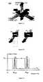
- FIG. 2 ashows the operation of the Hall Effect on a semiconductor system.
- a semiconductor platelet 240 having a current 230 flowing through itis subjected to a magnetic flux 210 .
- This magnetic fluxacts perpendicularly (at 90 degree angle) to the current flow, and results in a Hall voltage 220 at a 90 degree angle to both the magnetic flux 210 and the current 230 .
- FIG. 2 bshows where a magnetic flux component 250 perpendicular to the chip surface 270 is measured.
- the chip surface 270is encapsulated inside the package 260 .
- FIG. 2 cshows a graph of output voltage (vertical axis) versus magnetic pole location (horizontal axis) in the package 240 .
- the output voltageturns low (position 280 on the graph) when the magnetic south pole is on the branded side of the package.
- the output voltage (position 290 on the graph)turns high if the magnetic field is removed.
- the sensor chip 270does not respond to a magnetic north pole on the branded side of package 260 .
- Other Hall-effect sensor chipswhich pole independent and so respond to either a magnetic north pole or a magnetic south pole could also be utilized with this invention, one such devise is the Allegro A3211 device, from AllegroMicroSystems, Inc. of Worcester, Mass.
- FIG. 3shows a wireless peripheral device 300 , for use with an improved wireless bind system and method.
- the wireless peripheral device 300comprises a proximity sensor 310 coupled to a transmit circuit 320 .
- the wireless peripheral device 300may further comprise a bind circuit 330 coupled to proximity sensor 310 and transmit circuit 320 .
- the proximity sensor 310is a magnetic sensor, such as a semiconductor hall effect sensor or a mechanical sensor like a reed switch.
- the proximity sensor 310may be a electrical field sensor, which triggers when placed in proximity to an electrical field.
- the proximity sensor 310could be an optical switch that triggers when light shines or reflects on the sensor.
- the wireless device 300may be configured to trigger the proximity sensor 310 on receiving light of a certain frequency, or on receiving a certain pattern (pulses) of light on the sensor.
- the proximity sensor 310may trigger when in the presence of an audio frequency or wave of a certain frequency or frequency range. In one embodiment, this audio frequency may be above or below the threshold of human hearing.
- the wireless peripheral device 300may be a peripheral such as camera, a sensor for sensing one or more of an electrical field, a current, a capacitance, a light intensity, a visual image, a temperature, a pressure, a weight or any other physical or electrical property.
- the sensormay also be a debit/credit/payment/identification card reader, a bar code reader, a smart chip reader, a RFID tag reader or one of many other one-way (transmit only) devices.
- the wireless peripheral device 300may be a human interface device such as a mouse, a keyboard, a joystick, a touchpad, a microphone, a musical instrument or pickup, a game controller, a visual input device (camera or motion recognition), a steering wheel controller, eye motion input device, or other input device.
- a human interface devicesuch as a mouse, a keyboard, a joystick, a touchpad, a microphone, a musical instrument or pickup, a game controller, a visual input device (camera or motion recognition), a steering wheel controller, eye motion input device, or other input device.
- the wireless communication device 300comprises a proximity sensor 310 configurable to detect a proximity to another wireless device 400 .
- the proximity sensor 310may detect when another wireless device 400 is within a range of 3 inches.
- the proximity sensor 310may detect when another wireless device 400 is within a range of 12 inches.
- the proximity sensor 310may detect when another wireless device 400 is within a range of 48 inches.
- the wireless communication device 300may further comprise a bind circuit 330 configurable to initiate a bind operation; and a transmit circuit 320 configurable to transmit bind signals to another wireless device 400 .
- the bind circuit 330may further comprise logic controlling a power of the output from transmit block 320 .
- the bind logic 330may further comprise logic controlling a number of channels on which bind signals are transmitted.
- the bind circuit 330may further comprise pseudorandom number (PN) logic controlling a number of PN codes transmitted in the bind signals.
- PN codesare just another way to divide the available frequencies and bandwidth. To prevent false tripping, the bind circuit may commence a bind operation on detection a signature of magnetic or electrical pulses or patterns.
- FIG. 4shows a wireless host device 400 for use with an improved wireless bind system and method.
- the wireless host device 400comprises a receive circuit 410 coupled to a proximity sensor activator 420 .
- the receive circuitis configurable to receive wireless communications from a peripheral device 300 .
- the proximity sensor activator 420is configurable to cause a sensor 310 to trip when the sensor is in proximity to the host device 400 .
- the proximity sensor activator 420has a magnetic field.
- the proximity sensor activatormay comprise a dedicated magnet or magnetic strip, or a magnetic field generated by a monitor or speaker or other electromagnetic device associated with the wireless host device 400 .
- the proximity sensor activator 420may comprise an electrical field generator, which causes a proximity sensor 310 to trigger when placed in proximity to an electrical field.
- the proximity sensor activator 420could be an optical source that causes a proximity sensor 310 of the peripheral device to trigger when light from the sensor activator 420 shines or reflects on the sensor 310 .
- the proximity sensor activator 420may be configured to generate light of a certain frequency, or to generate a certain pattern (pulses) of light, or a combination thereof.
- the proximity sensor activator 420may generate an audio frequency or wave of a certain frequency or frequency range. In one embodiment, this audio frequency may be above the threshold of human hearing.
- the wireless peripheral device 400may further comprise a processor circuit 430 .
- the wireless host device 400may be a personal computer (PC), server, workstation, laptop, cellphone, personal digital assistant (PDA), games console, media playback or display device, communications or network device, security control device, industrial control device, automotive interface or control device, or other host device with which a peripheral may be used.
- the proximity sensor activator 420may in one embodiment be located inside the wireless host device 400 .
- the improved solutioncomprising the wireless peripheral device 300 and the wireless host device 400 operate in the following manner.
- the switch proximity sensor 310 in the peripheral 300opens signaling the peripheral 300 to enter pairing mode.
- the peripheral 300may optionally reduce transmit power from the transmit circuit 320 , which reduces the communication range to the area immediately surrounding the peripheral 300 ensuring that the peripheral 300 will not pair with another host that is within normal communication range, but is not the desired host.
- the peripheral 300then transmits a pairing mode request message on one or more channels, and may repeat this message on one or more channels a plurality of times.
- the pairing mode (bind) request messagecontains information concerning the channel to use for data communication and any other necessary information to allow the peripheral to communicate with the host such as encryption key, checksum seed, or similar key.
- the peripheral 300transmits a pairing message (multiple times to guarantee that the host has received the message) on the pairing channel that contains information about the channel the peripheral will use. When the host 400 receives this message it moves to the new channel and is able to receive data from the peripheral 300 .
- FIG. 5shows a wireless host 500 having a proximity sensor activator 520 external to the wireless host 500 .
- the proximity sensor activator 520is in a ‘dongle’ device attached to the wireless host device.
- the proximity sensor activatormay be located in the vicinity of the host device (e.g. in or on a desk where the host device is located).
- the proximity sensor activator 520may comprise a monitor or a speaker device usually associated with the host.
- the proximity sensor activator 520may comprise a magnetic strip or button or element that is provided with the wireless peripheral device, and which is intended to be placed by the user in a location proximate to the wireless host, or wherever else is convenient for binding to the host.
- the desired proximity rangewill vary depending on the specific application and may not require reduction in the receive sensitivity on the wireless host or wireless peripheral device.
- the maximum allowed bind rangemay be up to maximum transmit/receive range of the transmit circuit.
- the binding processcould be initiated not through a proximity sensor, but rather by a touch sensor on the peripheral that is activated when touched against an electrical connector or pad on the host device.
- FIG. 6illustrates an alternative embodiment of a binding system 600 having a wireless peripheral 610 and wireless host 650 each having a connector or contact for initiating a bind operation.
- the wireless peripheral 610comprises a bind circuit 620 , a transmit circuit 630 , and a first connector or contact 640 .
- the wireless host 650comprises a receive circuit 660 , a processor 670 , and a second connector or contact 680 .
- the connector or contact 640(on the wireless peripheral 610 ) may be conductive, so that when it is touched against a corresponding connector or contact 680 on the wireless host device 650 , a bind operation is initiated. Because when the connector or contact 640 and 680 are in contact they have a conductive path through them, both unidirectional and/or bi-directional communication may occur between the peripheral 610 and host 650 .
- the first connector or contact 640 and the second connector or contact 680may form a single conductive path or may form a plurality of conductive paths, and may communicate using a serial interface (for example the well known I2C interface, or a serial interface) or a parallel interface, or even a single wire interface.
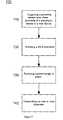
- FIG. 7An improved method 700 of binding a wireless peripheral device 300 to a wireless host device 400 is shown in FIG. 7 .
- a first step 710triggering a proximity sensor 310 on close proximity of the peripheral device 300 to the host device 400 .
- a second step 720comprises initiating a bind operation by the peripheral device 300 to the host device 400 .
- a third optional step 730may comprise reducing the transmission range or transmission power of the transmit circuit 320 .
- a fourth step 740comprises transmitting a bind message on one or more channels, where the data to be transmitted may comprise one or more pseudorandom number (PN) codes.
- PNpseudorandom number
- Embodiments of the present inventionare well suited to performing various other steps or variations of the steps recited herein, and in a sequence other than that depicted and/or described herein. In one embodiment, such a process is carried out by processors and other electrical and electronic components, e.g., executing computer readable and computer executable instructions comprising code contained in a computer usable medium.
Landscapes
- Engineering & Computer Science (AREA)
- General Engineering & Computer Science (AREA)
- Theoretical Computer Science (AREA)
- Human Computer Interaction (AREA)
- Physics & Mathematics (AREA)
- General Physics & Mathematics (AREA)
- Input From Keyboards Or The Like (AREA)
- Mobile Radio Communication Systems (AREA)
Abstract
Description
Claims (21)
Priority Applications (1)
| Application Number | Priority Date | Filing Date | Title |
|---|---|---|---|
| US11/240,936US8044928B2 (en) | 2005-09-29 | 2005-09-29 | Method for pairing 1-way devices |
Applications Claiming Priority (1)
| Application Number | Priority Date | Filing Date | Title |
|---|---|---|---|
| US11/240,936US8044928B2 (en) | 2005-09-29 | 2005-09-29 | Method for pairing 1-way devices |
Publications (2)
| Publication Number | Publication Date |
|---|---|
| US20070070035A1 US20070070035A1 (en) | 2007-03-29 |
| US8044928B2true US8044928B2 (en) | 2011-10-25 |
Family
ID=37893249
Family Applications (1)
| Application Number | Title | Priority Date | Filing Date |
|---|---|---|---|
| US11/240,936Active2028-06-15US8044928B2 (en) | 2005-09-29 | 2005-09-29 | Method for pairing 1-way devices |
Country Status (1)
| Country | Link |
|---|---|
| US (1) | US8044928B2 (en) |
Cited By (2)
| Publication number | Priority date | Publication date | Assignee | Title |
|---|---|---|---|---|
| US20100262696A1 (en)* | 2007-11-07 | 2010-10-14 | Nec Corporation | Pairing system, pairing management device, pairing method, and program |
| US9912978B2 (en) | 2013-07-29 | 2018-03-06 | Apple Inc. | Systems, methods, and computer-readable media for transitioning media playback between multiple electronic devices |
Families Citing this family (17)
| Publication number | Priority date | Publication date | Assignee | Title |
|---|---|---|---|---|
| US7940933B2 (en)* | 2006-08-18 | 2011-05-10 | Medtronic, Inc. | Secure telemetric link |
| US9000914B2 (en) | 2010-03-15 | 2015-04-07 | Welch Allyn, Inc. | Personal area network pairing |
| US8957777B2 (en) | 2010-06-30 | 2015-02-17 | Welch Allyn, Inc. | Body area network pairing improvements for clinical workflows |
| US8907782B2 (en)* | 2010-06-30 | 2014-12-09 | Welch Allyn, Inc. | Medical devices with proximity detection |
| CN102361512B (en)* | 2011-06-30 | 2013-08-07 | 华为终端有限公司 | Device, method and system for binding terminal |
| GB201116571D0 (en)* | 2011-09-26 | 2011-11-09 | Bytec Group Ltd | Wireless data input system |
| US9317455B2 (en)* | 2012-01-05 | 2016-04-19 | Lenovo (Singapore) Pte. Ltd. | Virtual switching of information handling device components |
| US8913955B1 (en)* | 2012-09-17 | 2014-12-16 | Amazon Technologies, Inc. | Magnetically initiated device pairing |
| US9312949B1 (en)* | 2013-03-05 | 2016-04-12 | Square, Inc. | Pairing techniques for a wireless card reader |
| US9232409B2 (en)* | 2013-12-12 | 2016-01-05 | Microsoft Technology Licensing, Llc | Binding of an apparatus to a computing device |
| US11481750B2 (en) | 2015-06-30 | 2022-10-25 | Block, Inc. | Pairing a payment object reader with a point-of-sale terminal |
| US12207322B2 (en) | 2015-09-24 | 2025-01-21 | Block, Inc. | Server-assisted pairing for wireless communications |
| US11087315B2 (en) | 2015-09-24 | 2021-08-10 | Square, Inc. | Server-assisted pairing for wireless communications |
| US11871237B1 (en) | 2016-06-30 | 2024-01-09 | Block, Inc. | Pairing a payment object reader with a point-of-sale terminal |
| DE102016115005A1 (en)* | 2016-08-12 | 2018-02-15 | Endress + Hauser Gmbh + Co. Kg | System and method for activating a radio interface of a field device of process automation |
| US11310848B2 (en) | 2017-08-31 | 2022-04-19 | Huawei Technologies Co., Ltd. | Pairing method, unpairing method, terminal device, and externally-connected device |
| CN110314283A (en)* | 2018-03-28 | 2019-10-11 | 苏州景昱医疗器械有限公司 | A kind of method and apparatus of creation wireless communication |
Citations (10)
| Publication number | Priority date | Publication date | Assignee | Title |
|---|---|---|---|---|
| US5339095A (en)* | 1991-12-05 | 1994-08-16 | Tv Interactive Data Corporation | Multi-media pointing device |
| US5854621A (en)* | 1991-03-19 | 1998-12-29 | Logitech, Inc. | Wireless mouse |
| US5881366A (en)* | 1996-05-01 | 1999-03-09 | Logitech, Inc. | Wireless peripheral interface |
| US6473070B2 (en)* | 1998-11-03 | 2002-10-29 | Intel Corporation | Wireless tracking system |
| US20040015625A1 (en)* | 2001-05-15 | 2004-01-22 | Yuji Ayatsuka | Method for connecting computer body to wireless peripheral, computer, and wireless peripheral |
| US20040233168A1 (en)* | 2003-05-19 | 2004-11-25 | Gateway, Inc. | System and methods for interacting with a supplemental hand-held mouse |
| US20050243059A1 (en)* | 2004-03-16 | 2005-11-03 | Morris Martin G | High-reliability computer interface for wireless input devices |
| US20060125806A1 (en)* | 2004-09-27 | 2006-06-15 | The Regents Of The University Of Minnesota | Human-activated displacement control appliance for use with computerized device/mechanism |
| US20060132433A1 (en)* | 2000-04-17 | 2006-06-22 | Virtual Technologies, Inc. | Interface for controlling a graphical image |
| US7436965B2 (en)* | 2003-02-19 | 2008-10-14 | Microsoft Corporation | Optical out-of-band key distribution |
- 2005
- 2005-09-29USUS11/240,936patent/US8044928B2/enactiveActive
Patent Citations (10)
| Publication number | Priority date | Publication date | Assignee | Title |
|---|---|---|---|---|
| US5854621A (en)* | 1991-03-19 | 1998-12-29 | Logitech, Inc. | Wireless mouse |
| US5339095A (en)* | 1991-12-05 | 1994-08-16 | Tv Interactive Data Corporation | Multi-media pointing device |
| US5881366A (en)* | 1996-05-01 | 1999-03-09 | Logitech, Inc. | Wireless peripheral interface |
| US6473070B2 (en)* | 1998-11-03 | 2002-10-29 | Intel Corporation | Wireless tracking system |
| US20060132433A1 (en)* | 2000-04-17 | 2006-06-22 | Virtual Technologies, Inc. | Interface for controlling a graphical image |
| US20040015625A1 (en)* | 2001-05-15 | 2004-01-22 | Yuji Ayatsuka | Method for connecting computer body to wireless peripheral, computer, and wireless peripheral |
| US7436965B2 (en)* | 2003-02-19 | 2008-10-14 | Microsoft Corporation | Optical out-of-band key distribution |
| US20040233168A1 (en)* | 2003-05-19 | 2004-11-25 | Gateway, Inc. | System and methods for interacting with a supplemental hand-held mouse |
| US20050243059A1 (en)* | 2004-03-16 | 2005-11-03 | Morris Martin G | High-reliability computer interface for wireless input devices |
| US20060125806A1 (en)* | 2004-09-27 | 2006-06-15 | The Regents Of The University Of Minnesota | Human-activated displacement control appliance for use with computerized device/mechanism |
Non-Patent Citations (1)
| Title |
|---|
| A3211 and A3212 Micropower, Ultra-Sensitive Hal-Effect Switches, Allegro Microsystems, Inc., A3211-DS, Rev. 1, Copyright © 2002, 2003, 2004, 2005 Allegro Microsystems, Inc., 15 pages. |
Cited By (3)
| Publication number | Priority date | Publication date | Assignee | Title |
|---|---|---|---|---|
| US20100262696A1 (en)* | 2007-11-07 | 2010-10-14 | Nec Corporation | Pairing system, pairing management device, pairing method, and program |
| US8850031B2 (en)* | 2007-11-07 | 2014-09-30 | Nec Corporation | Pairing system, pairing management device, pairing method, and program |
| US9912978B2 (en) | 2013-07-29 | 2018-03-06 | Apple Inc. | Systems, methods, and computer-readable media for transitioning media playback between multiple electronic devices |
Also Published As
| Publication number | Publication date |
|---|---|
| US20070070035A1 (en) | 2007-03-29 |
Similar Documents
| Publication | Publication Date | Title |
|---|---|---|
| US8044928B2 (en) | Method for pairing 1-way devices | |
| KR101797643B1 (en) | Instruction information transmission and reception methods and devices thereof | |
| CN103413218B (en) | Mobile terminal, NFC payment, apparatus and system | |
| US9042814B2 (en) | Measurement and reporting of received signal strength in NFC-enabled devices | |
| US20150312879A1 (en) | Indication of nfc location | |
| US10551967B2 (en) | Two-way communication between an electronic card and a touchscreen device | |
| KR20110000666A (en) | Method and apparatus for automatic application selection using a plurality of discovery managers in an electronic device | |
| CN105518572B (en) | Wearable computing devices | |
| US12340061B2 (en) | User-worn device and touch-device for ultrasonic data transmission | |
| KR102206877B1 (en) | Method and apparatus for displaying biometric information | |
| WO2006034143A2 (en) | A contactless card reader integrated into a touchpad | |
| KR20170094748A (en) | Electronic device having loop antenna | |
| CN109271830B (en) | Fingerprint sensing integrated circuit | |
| CN113989963B (en) | Signal processing method and related equipment | |
| KR102845161B1 (en) | Electronic device identifying characteristics of object by using millimeter wave and method for controlling thereof | |
| CN105574373B (en) | Mobile device, for making trade convenient method and system | |
| Xue et al. | MagneComm+: Near-field electromagnetic induction communication with magnetometer | |
| CN103368612A (en) | Targeted muting for communication between electronic appliances | |
| KR101754231B1 (en) | Method, apparatus and computer program for bidirectional communication with using Dual interface NFC tag | |
| KR102196964B1 (en) | Wearable device, wristwatch, and short distance communication switch method | |
| US20150061836A1 (en) | Assignable switch for portable devices | |
| Kasper et al. | Embedded security analysis of RFID devices | |
| CN106897641B (en) | Information image display method and device | |
| US9870078B2 (en) | Touch panel device controlling method and touch panel device | |
| KR101950806B1 (en) | Input apparatus and method for touch panel |
Legal Events
| Date | Code | Title | Description |
|---|---|---|---|
| AS | Assignment | Owner name:CYPRESS SEMICONDUCTOR CORPORATION, CALIFORNIA Free format text:ASSIGNMENT OF ASSIGNORS INTEREST;ASSIGNORS:ASBURY, RAY;WOODINGS, RYAN WINFIELD;REEL/FRAME:017059/0971 Effective date:20050928 | |
| STCF | Information on status: patent grant | Free format text:PATENTED CASE | |
| AS | Assignment | Owner name:MORGAN STANLEY SENIOR FUNDING, INC., NEW YORK Free format text:SECURITY INTEREST;ASSIGNORS:CYPRESS SEMICONDUCTOR CORPORATION;SPANSION LLC;REEL/FRAME:035240/0429 Effective date:20150312 | |
| FPAY | Fee payment | Year of fee payment:4 | |
| MAFP | Maintenance fee payment | Free format text:PAYMENT OF MAINTENANCE FEE, 8TH YEAR, LARGE ENTITY (ORIGINAL EVENT CODE: M1552); ENTITY STATUS OF PATENT OWNER: LARGE ENTITY Year of fee payment:8 | |
| AS | Assignment | Owner name:MUFG UNION BANK, N.A., CALIFORNIA Free format text:ASSIGNMENT AND ASSUMPTION OF SECURITY INTEREST IN INTELLECTUAL PROPERTY;ASSIGNOR:MORGAN STANLEY SENIOR FUNDING, INC.;REEL/FRAME:050896/0366 Effective date:20190731 | |
| AS | Assignment | Owner name:MORGAN STANLEY SENIOR FUNDING, INC., NEW YORK Free format text:CORRECTIVE ASSIGNMENT TO CORRECT THE 8647899 PREVIOUSLY RECORDED ON REEL 035240 FRAME 0429. ASSIGNOR(S) HEREBY CONFIRMS THE SECURITY INTERST;ASSIGNORS:CYPRESS SEMICONDUCTOR CORPORATION;SPANSION LLC;REEL/FRAME:058002/0470 Effective date:20150312 | |
| AS | Assignment | Owner name:SPANSION LLC, CALIFORNIA Free format text:RELEASE BY SECURED PARTY;ASSIGNOR:MUFG UNION BANK, N.A.;REEL/FRAME:059410/0438 Effective date:20200416 Owner name:CYPRESS SEMICONDUCTOR CORPORATION, CALIFORNIA Free format text:RELEASE BY SECURED PARTY;ASSIGNOR:MUFG UNION BANK, N.A.;REEL/FRAME:059410/0438 Effective date:20200416 | |
| MAFP | Maintenance fee payment | Free format text:PAYMENT OF MAINTENANCE FEE, 12TH YEAR, LARGE ENTITY (ORIGINAL EVENT CODE: M1553); ENTITY STATUS OF PATENT OWNER: LARGE ENTITY Year of fee payment:12 |