US8044448B2 - Nonvolatile semiconductor memory device - Google Patents
Nonvolatile semiconductor memory deviceDownload PDFInfo
- Publication number
- US8044448B2 US8044448B2US12/508,904US50890409AUS8044448B2US 8044448 B2US8044448 B2US 8044448B2US 50890409 AUS50890409 AUS 50890409AUS 8044448 B2US8044448 B2US 8044448B2
- Authority
- US
- United States
- Prior art keywords
- layer
- memory cell
- region
- conductive layer
- interconnection
- Prior art date
- Legal status (The legal status is an assumption and is not a legal conclusion. Google has not performed a legal analysis and makes no representation as to the accuracy of the status listed.)
- Active, expires
Links
Images


Classifications
- H—ELECTRICITY
- H10—SEMICONDUCTOR DEVICES; ELECTRIC SOLID-STATE DEVICES NOT OTHERWISE PROVIDED FOR
- H10D—INORGANIC ELECTRIC SEMICONDUCTOR DEVICES
- H10D89/00—Aspects of integrated devices not covered by groups H10D84/00 - H10D88/00
- H10D89/10—Integrated device layouts
- G—PHYSICS
- G11—INFORMATION STORAGE
- G11C—STATIC STORES
- G11C5/00—Details of stores covered by group G11C11/00
- G11C5/02—Disposition of storage elements, e.g. in the form of a matrix array
- G11C5/025—Geometric lay-out considerations of storage- and peripheral-blocks in a semiconductor storage device
- G—PHYSICS
- G11—INFORMATION STORAGE
- G11C—STATIC STORES
- G11C5/00—Details of stores covered by group G11C11/00
- G11C5/06—Arrangements for interconnecting storage elements electrically, e.g. by wiring
- G11C5/063—Voltage and signal distribution in integrated semi-conductor memory access lines, e.g. word-line, bit-line, cross-over resistance, propagation delay
- H—ELECTRICITY
- H10—SEMICONDUCTOR DEVICES; ELECTRIC SOLID-STATE DEVICES NOT OTHERWISE PROVIDED FOR
- H10B—ELECTRONIC MEMORY DEVICES
- H10B41/00—Electrically erasable-and-programmable ROM [EEPROM] devices comprising floating gates
- H10B41/10—Electrically erasable-and-programmable ROM [EEPROM] devices comprising floating gates characterised by the top-view layout
- H—ELECTRICITY
- H10—SEMICONDUCTOR DEVICES; ELECTRIC SOLID-STATE DEVICES NOT OTHERWISE PROVIDED FOR
- H10B—ELECTRONIC MEMORY DEVICES
- H10B41/00—Electrically erasable-and-programmable ROM [EEPROM] devices comprising floating gates
- H10B41/20—Electrically erasable-and-programmable ROM [EEPROM] devices comprising floating gates characterised by three-dimensional arrangements, e.g. with cells on different height levels
- H10B41/23—Electrically erasable-and-programmable ROM [EEPROM] devices comprising floating gates characterised by three-dimensional arrangements, e.g. with cells on different height levels with source and drain on different levels, e.g. with sloping channels
- H10B41/27—Electrically erasable-and-programmable ROM [EEPROM] devices comprising floating gates characterised by three-dimensional arrangements, e.g. with cells on different height levels with source and drain on different levels, e.g. with sloping channels the channels comprising vertical portions, e.g. U-shaped channels
- H—ELECTRICITY
- H10—SEMICONDUCTOR DEVICES; ELECTRIC SOLID-STATE DEVICES NOT OTHERWISE PROVIDED FOR
- H10B—ELECTRONIC MEMORY DEVICES
- H10B41/00—Electrically erasable-and-programmable ROM [EEPROM] devices comprising floating gates
- H10B41/40—Electrically erasable-and-programmable ROM [EEPROM] devices comprising floating gates characterised by the peripheral circuit region
- H—ELECTRICITY
- H10—SEMICONDUCTOR DEVICES; ELECTRIC SOLID-STATE DEVICES NOT OTHERWISE PROVIDED FOR
- H10B—ELECTRONIC MEMORY DEVICES
- H10B69/00—Erasable-and-programmable ROM [EPROM] devices not provided for in groups H10B41/00 - H10B63/00, e.g. ultraviolet erasable-and-programmable ROM [UVEPROM] devices
- H—ELECTRICITY
- H10—SEMICONDUCTOR DEVICES; ELECTRIC SOLID-STATE DEVICES NOT OTHERWISE PROVIDED FOR
- H10D—INORGANIC ELECTRIC SEMICONDUCTOR DEVICES
- H10D86/00—Integrated devices formed in or on insulating or conducting substrates, e.g. formed in silicon-on-insulator [SOI] substrates or on stainless steel or glass substrates
- H10D86/201—Integrated devices formed in or on insulating or conducting substrates, e.g. formed in silicon-on-insulator [SOI] substrates or on stainless steel or glass substrates the substrates comprising an insulating layer on a semiconductor body, e.g. SOI
Definitions
- the present inventionrelates to a nonvolatile semiconductor memory device in which data can be electrically reprogrammed.
- 3D laminated cell structuresSemiconductor memory devices of recent years tend to increase the number of bits (the number of memory cells) to increase the amount of data programmed to one chip. Therefore, in recent years, many semiconductor memory devices are proposed having structures in which memory cells are disposed three dimensionally (hereinbelow referred to as “3D laminated cell structures”) to increase the integration of memory (refer to JP-A 2007-266143 (Kokai), U.S. Pat. No. 5,599,724, and U.S. Pat. No. 5,707,885).
- an HV transistoris indispensable to breakdown against the high voltage.
- an HV transistoris used as a transfer gate transistor connected to a word line, it is necessary that the number of transistors is the same as the number of word lines. Accordingly, it is difficult to reduce the occupied surface area of the entire chip due to the occupied surface area of the HV transistor.
- the occupied surface area of the HV transistorbecomes a problem in the case where a 3D laminated cell structure is formed.
- a NAND flash memoryfor example, using a floating gate as the memory layer and a MONOS (Metal-Oxide-Nitride-Oxide-Semiconductor) nonvolatile semiconductor memory device using silicon nitride and the like as the memory layer, laminating the memory cell portion may be considered to increase the memory density.
- JP-A 2007-180389discusses technology in regard to a laminated nonvolatile semiconductor memory device that includes multiple memory cell strings in which a semiconductor is formed in a pillar configuration perpendicular to a semiconductor substrate and multiple memory cells are connected in series.
- a control gate of the memory cellis connected to a word line; the word line is drawn out to a peripheral circuit region; and a prescribed operation is performed. Then, the word line is provided at a density according to the arrangement density of the memory cells.
- a transfer gate transistoris provided in the peripheral circuit region, generally, the size of the transfer gate transistor is larger than the distance between the word lines.
- a nonvolatile semiconductor memory deviceincluding: a memory cell array region having memory cells connected in series; a control circuit region disposed below the memory cell array region; and an interconnection portion electrically connecting the control circuit region and the memory cell array region, the memory cell array region including: a plurality of first memory cell regions having the memory cells; and a plurality of connection regions, the interconnection portion being provided in the connection regions, the first memory cell regions being provided at a first pitch in a first direction orthogonal to a lamination direction of the memory cell array region and the control circuit region; and the connection regions being provided between the first memory cell regions mutually adjacent in the first direction, and at a second pitch in a second direction orthogonal to the lamination direction and the first direction.
- a nonvolatile semiconductor memory deviceincluding: a semiconductor substrate including a memory cell region and a peripheral circuit region provided adjacent to the memory cell region; a memory cell string including a plurality of memory cells connected in series in a direction perpendicular to a major surface of the semiconductor substrate in the memory cell region; a transistor provided on the semiconductor substrate in the peripheral circuit region; and a plurality of first interconnections being extension portions of first conductive layers forming control gates of the memory cells, the first conductive layers extending in a first direction as viewed from the semiconductor substrate, the extension portions of first conductive layers extending to the peripheral circuit region, the first interconnections passing above a gate electrode of the transistor as viewed from the semiconductor substrate.
- a nonvolatile semiconductor memory deviceincluding: a semiconductor substrate including a memory cell region and a peripheral circuit region provided adjacent to the memory cell region; a memory cell string including a plurality of memory cells connected in series in a direction perpendicular to a major surface of the semiconductor substrate in the memory cell region; a transistor provided on the semiconductor substrate in the peripheral circuit region; an inter-layer connection part being provided on the semiconductor substrate in the peripheral circuit region, the inter-layer connection part extending in a direction non-parallel to the major surface and electrically connecting to a diffusion layer of the transistor; and a peripheral circuit region interconnection being an extension portion of a conductive layer forming a control gate of the memory cell, the extension portion extending to the peripheral circuit region, the peripheral circuit region interconnection being provided in the peripheral circuit region and extending in a first direction parallel to the major surface of the semiconductor substrate, the peripheral circuit region interconnection including a connection portion protruding parallel to the major surface in a second direction non-parallel to the first
- FIG. 1is a schematic view of a nonvolatile semiconductor memory device according to a first embodiment of the invention
- FIG. 2Ais a circuit diagram of a memory array layer 400 according to the first embodiment
- FIG. 2Bis a schematic perspective view showing a memory unit Ut
- FIG. 3is a schematic top view of the memory cell array layer 400 of the nonvolatile semiconductor memory device according to the first embodiment
- FIG. 4is an enlarged view of the portion A of FIG. 3 ;
- FIG. 5is an enlarged view of the portion B of FIG. 3 ;
- FIG. 6 and FIG. 7are views of FIG. 5 minus omitted portions
- FIG. 8is a cross-sectional view along the line I-I′ of FIG. 5 ;
- FIG. 9is a cross-sectional view along the line II-II′ of FIG. 5 ;
- FIG. 10is a cross-sectional view along the line III-III′ of FIG. 5 ;
- FIG. 11is a cross-sectional view along the line IV-IV′ of FIG. 5 ;
- FIG. 12is a cross-sectional view along the line V-V′ of FIG. 5 ;
- FIG. 13is a schematic top view of a memory cell array layer 400 A of the nonvolatile semiconductor memory device according to a second embodiment of the invention.
- FIG. 14is an enlarged view of the portion C of FIG. 13 ;
- FIG. 15is an enlarged view of the portion D of FIG. 13 ;
- FIG. 16 and FIG. 17are views of FIG. 15 minus omitted portions
- FIG. 18is a cross-sectional view along the line VI-VI′ of FIG. 15 ;
- FIG. 19is a cross-sectional view along the line VII-VII′ of FIG. 15 ;
- FIG. 20is a cross-sectional view along the line VIII-VIII′ of FIG. 15 ;
- FIG. 21is a cross-sectional view along the line IX-IX′ of FIG. 15 ;
- FIG. 22is a cross-sectional view along the line X-X′ of FIG. 15 ;
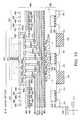
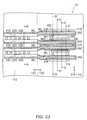
- FIG. 23is a schematic plan view illustrating the configuration of a nonvolatile semiconductor memory device according to a third embodiment of the invention.
- FIG. 24is a cross-sectional view along the line A-A′ of FIG. 23 ;
- FIG. 25is a cross-sectional view along the line B-B′ of FIG. 23 ;
- FIG. 26is a cross-sectional view along the line C-C′ of FIG. 23 ;
- FIG. 27is a cross-sectional view along the line D-D′ of FIG. 23 ;
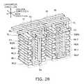
- FIG. 28is a cross-sectional view along the line E-E′ of FIG. 23 ;
- FIG. 29is a schematic perspective view illustrating the configuration of a portion of the nonvolatile semiconductor storage device according to the third embodiment of the invention.
- FIG. 30is a schematic perspective view illustrating the configuration of a portion of another nonvolatile semiconductor storage device according to the third embodiment of the invention.
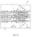
- FIG. 31is a schematic plan view illustrating the configuration of a nonvolatile semiconductor memory device according to a fourth embodiment of the invention.
- FIG. 32is a cross-sectional view along the line B-B′ of FIG. 31 ;
- FIG. 33is a cross-sectional view along the line C-C′ of FIG. 31 ;
- FIG. 34is a cross-sectional view along the line D-D′ of FIG. 31 ;
- FIG. 35is a cross-sectional view along the line E-E′ of FIG. 31 ;
- FIG. 36is a schematic plan view illustrating the configuration of a nonvolatile semiconductor memory device according to a fifth embodiment of the invention.
- FIG. 37is a schematic plan view illustrating the configuration of another nonvolatile semiconductor memory device according to the fifth embodiment of the invention.
- FIG. 38is a schematic plan view illustrating the configuration of another nonvolatile semiconductor memory device according to the fifth embodiment of the invention.
- FIG. 39is a schematic plan view illustrating the configuration of another nonvolatile semiconductor memory device according to the fifth embodiment of the invention.
- FIG. 40is a schematic plan view illustrating the configuration of a nonvolatile semiconductor memory device according to a sixth embodiment of the invention.
- FIG. 1is a schematic view of a nonvolatile semiconductor memory device according to a first embodiment of the invention.
- the nonvolatile semiconductor memory device according to the first embodimentincludes a semiconductor substrate 100 , a control circuit layer 200 sequentially formed on an upper portion of the semiconductor substrate 100 , a support layer 300 , and a memory cell array layer 400 .
- the memory cell array layer 400includes a memory cell array.
- the nonvolatile semiconductor memory devicealso includes an interconnection portion 500 that electrically connects the control circuit layer 200 and the memory cell array layer 400 .
- the interconnection portion 500passes through the support layer 300 , extends into the memory cell array layer 400 , and connects to the memory cell array.
- the control circuit layer 200functions as a control circuit that controls an operation of the memory cell array layer 400 .
- the control circuit layer 200includes a function that controls a voltage applied to a memory cell included in the memory cell array layer 400 .
- the control circuit layer 200includes, for example, a transfer transistor that transfers a high voltage from a row decoder to a word line of the memory cell.
- the control circuit layer 200includes, for example, a row decoder unit 200 A, a sense amplifier unit 200 B, and the like.
- the row decoder unit 200 Afunctions as a row decoder that drives an electrical potential of a word line WL (referring to FIG. 2A and FIG. 2B described below) provided in the memory cell array layer 400 to an “H” (high level) or an “L” (low level).
- the sense amplifier unit 200 Bfunctions as a sense amplifier that senses and amplifies a signal from a bit line BL (referring to FIG. 2A and FIG. 2B described below) of the memory cell array layer 400 .
- the control circuit layer 200may include, for example, a portion that functions as a column decoder and the like.
- the memory cell array layer 400includes a first memory cell region 40 A, a first non-memory cell region 40 B, and a connection region 40 C.
- the first memory cell region 40 Ais a region including a memory unit Ut (memory cells MC) having a U-shaped 3D laminated cell structure.
- a memory cell arrayis formed by a collection of the memory units Ut.
- the non-memory cell region 40 Bis a region which does not include the memory unit Ut (the memory cells MC).
- the connection region 40 Cis regularly provided in a portion of the non-memory cell region 40 B.
- the interconnection portion 500 formed in a layer below the memory cell array layer 400 to electrically connect the control circuit layer 200 and the memory cell array layer 400is provided in (passes through) the connection region 40 C.
- the memory cell array layer 400is a so-called NAND flash memory.
- the memory unit Utwhich is one erasing unit of data, includes multiple electrically reprogrammable memory cells MC connected in series, a source-side selection transistor SST connected in series on one end (a source side) thereof, and a drain-side selection transistor SDT connected in series on another end (a drain side) thereof.
- eight memory cells MCare connected in series and form one memory unit Ut. Although eight memory cells MC are used in FIG. 2A , it goes without saying that other numbers may be used.
- Word lines WL 0 to WL 7are connected to control gates CG 0 to CG 7 of memory cell transistors as the memory cells MC.
- a source-side selection gate line SGSLis connected to a gate terminal of the source-side selection transistor SST.
- a source line SLis connected to a source terminal of the source-side selection transistor SST.
- a drain-side selection gate line SGDLis connected to a gate terminal of the drain-side selection transistor SDT.
- Bit lines BL 0 to BLiare connected to the drain terminals of the drain-side selection transistor SDT.
- the source-side selection gate line SGSLis used to control an ON/OFF of the source-side selection transistor SST.
- the drain-side selection gate line SGDLis used to control an ON/OFF of the drain-side selection transistor SDT.
- the source-side selection transistor SST and the drain-side selection transistor SDTfunction as gates for supplying a prescribed electrical potential to the memory cells MC in the memory unit Ut when programming data, reading data, etc.
- a memory block Bcincludes multiple memory units Ut arranged in a row direction (the direction in which the word lines extend). Multiple memory cells MC connected to the same word line WL in one memory block Bc are handled as one page. Operations of programming data and reading data are executed for each page.
- Multiple memory blocks Bcare arranged in a column direction (the direction in which the bit lines extend).
- the multiple memory blocks Bcare arranged to flip over in turn.
- a memory block Bc and a memory block Bc adjacent on one side theretoare disposed such that the drain-side selection transistors SDT face each other.
- the memory block Bc recited above and a memory block Bc adjacent on another side theretoare disposed such that the source-side selection transistors SST face each other.
- FIG. 2Bis a schematic perspective view illustrating the memory unit Ut of the nonvolatile semiconductor memory device according to the first embodiment.
- the memory units Utare disposed in a matrix configuration at prescribed pitches in the row direction and the column direction.
- the memory units Utare illustrated in two rows and two columns in FIG. 2B as an example.
- the memory unit Utincludes the word lines WL 0 to WL 7 , the source-side selection gate line SGSL, the drain-side selection gate line SGDL, a U-shaped semiconductor Se, a first contact electrode C 1 , and a second contact electrode C 2 .
- the word lines WL 0 to WL 7are formed in rectangular plate configurations extending in the row direction.
- the word lines WL 0 to WL 7are shared with the multiple memory units Ut juxtaposed in the row direction.
- the word lines WL 0 to WL 3are insulatively separated and laminated in order.
- the word lines WL 4 to WL 7are insulatively separated and laminated in order.
- the word lines WL 0 to WL 3 and the word lines WL 4 to WL 7are separated by a prescribed pitch in the column direction.
- the word line WL 0 and the word line WL 4are formed in the same layer.
- the word line WL 1 and the word line WL 5are formed in the same layer.
- the word line WL 2 and the word line WL 6are formed in the same layer.
- the word line WL 3 and the word line WL 7are formed in the same layer.
- the source-side selection gate line SGSL and the drain-side selection gate line SGDLare formed in rectangular plate configurations extending in the row direction.
- the source-side selection gate line SGSL and the drain-side selection gate line SGDLare shared by the multiple memory units Ut juxtaposed in the row direction.
- the source-side selection gate line SGSLis formed in a layer above the word line WL 3 and is insulatively separated.
- the drain-side selection gate line SGDLis formed in a layer above the word line WL 7 and is insulatively separated.
- the source-side selection gate line SGSL and the drain-side selection gate line SGDLare formed in the same layer.
- the U-shaped semiconductor Seis provided in each memory unit Ut.
- the U-shaped semiconductor Seis formed in a U-shape as viewed from the row direction.
- the U-shaped semiconductor Seis provided between the word lines WL 0 to WL 3 , and the word lines WL 4 to WL 7 , and between the source-side selection gate line SGSL on one side and the drain-side selection gate line SGDL on the other side.
- a charge storage layer that can store a chargeis provided between a side portion of the U-shaped semiconductor Se and the word lines WL 0 to WL 3 , and between a side portion of the U-shaped semiconductor Se and the word lines WL 4 to WL 7 .
- the side portions of the U-shaped semiconductor Seform memory cells MC 0 to MC 7 with the word lines WL 0 to WL 7 .
- Insulating layersare provided between the side portion of the U-shaped semiconductor Se and the source-side selection gate line SGSL, and between the side portion of the U-shaped semiconductor Se and the drain-side selection gate line SGDL.
- the side portion of the U-shaped semiconductor Seforms a source-side selection transistor SST with the source-side selection gate line SGSL; and the side portion of the U-shaped semiconductor Se forms the drain-side selection transistor SDT with the drain-side selection gate line SGDL.
- the first contact electrode C 1is provided in each memory unit Ut.
- the first contact electrode C 1is formed in a layer above the source-side selection gate line SGSL to contact one upper edge of each U-shaped semiconductor Se.
- the second contact electrode C 2is provided in each memory unit Ut.
- the second contact electrode C 2is formed in a layer above the drain-side selection gate line SGDL to contact the other upper edge of each U-shaped semiconductor Se.
- the source line SLis formed on an upper face of the first contact electrode C 1 .
- the source line SLis formed to extend in the row direction similarly to the word lines WL 0 to WL 7 .
- the source line SLis shared by the multiple memory units Ut juxtaposed in the row direction.
- a plug line PL having a pillar configuration extending into an upper layeris formed on an upper face of the second contact electrode C 2 .
- the bit line BL extending in the column directionis formed on an upper portion of the plug line PL.
- the bit line BLis shared by the multiple memory units Ut juxtaposed in the column direction.
- the extension direction of the bit lines BL described aboveis the column direction; and the extension direction of the source lines SL described above is the row direction.
- inter-layer insulating layersexist in regions not illustrated in FIG. 3 to FIG. 12 .
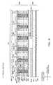
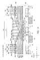
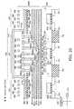
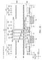
- FIG. 3is a schematic top view of the memory cell array layer 400 of the nonvolatile semiconductor memory device according to the first embodiment of the invention.
- FIG. 4is an enlarged view of the portion A of FIG. 3 .
- FIG. 5is an enlarged view of the portion B of FIG. 3 .
- FIG. 6 and FIG. 7are views of FIG. 5 minus omitted portions.
- a first source line conductive layer 403a second source line conductive layer 404 , and a bit line conductive layer 405 , to be described below, are omitted in FIG. 6 .
- FIG. 4is an enlarged view of the portion A of FIG. 3 .
- FIG. 5is an enlarged view of the portion B of FIG. 3 .
- FIG. 6 and FIG. 7are views of FIG. 5 minus omitted portions.
- a first source line conductive layer 403a second source line conductive layer 404 , and a bit line conductive layer 405 , to be described below, are omitted
- FIG. 8 to FIG. 12are cross-sectional views along lines I-I′ to V-V′ of FIG. 5 .
- the semiconductor substrate 100includes silicon (Si).
- the surface of the semiconductor substrate 100includes diffusion layers 101 formed at a prescribed spacing as illustrated in FIG. 10 to FIG. 12 .
- the diffusion layers 101include p-type or n-type impurity ions implanted into the semiconductor substrate 100 .
- the semiconductor substrate 100also includes an element separation insulating layer 102 that insulates between the diffusion layers 101 .
- the control circuit layer 200includes a gate insulating layer 201 and a gate conductive layer 202 .
- the gate insulating layer 201is formed to straddle the upper faces of a pair of adjacent diffusion layers 101 .
- the gate conductive layer 202is formed to contact an upper face of the gate insulating layer 201 .
- the gate insulating layer 201includes silicon oxide (SiO 2 ).
- the gate conductive layer 202includes polysilicon (p-Si).
- the gate conductive layer 202 and the diffusion layers 101 of the control circuit layer 200form a high voltage transistor Tr having the gate conductive layer 202 as a control gate and the diffusion layers 101 as a source and a drain.
- the high voltage transistor Tris, for example, the transfer gate transistor described above.
- the high voltage transistor Tris used in the row decoder unit 200 A, the sense amplifier unit 200 B, and the like described above.
- the high voltage transistor Tris connected as a transfer gate transistor to first to fourth word line conductive layers 401 a to 401 d described below via the interconnection portion 500 ( FIG. 1 ). As illustrated in FIG. 9 to FIG.
- the interconnection portion 500includes a lower interconnection layer 501 , an upper interconnection layer 502 , a first connection plug layer 503 a , a second connection plug layer 503 b , first connection plug layers 504 a and 504 b , a second connection plug layer 504 c , first connection plug layers 505 a and 505 b , a second connection plug layer 505 c , first connection plug layers 506 a and 506 b , and a second connection plug layer 506 c .
- the details of the configuration of the interconnection portion 500are described below.
- the support layer 300is formed on a portion above the control circuit layer 200 via an insulating layer of a prescribed thickness.
- the support layer 300includes, for example, aluminum oxide (Al 2 O 3 ).
- the memory cell array layer 400includes the first memory cell region 40 A, the first non-memory cell region 40 B, and the connection region 40 C.
- the first memory cell region 40 Ais a region including the memory cell MC.
- the non-memory cell region 40 Bis a region which does not include a memory cell MC.
- the connection region 40 Cis regularly provided in a portion of the first non-memory cell region 40 B.
- the interconnection portion 500( FIG. 1 ) formed in a layer below the memory cell array layer 400 to electrically connect the control circuit layer 200 and the memory cell array layer 400 is provided in (passes through) the connection region 40 C.
- the first memory cell region 40 Ais repeatedly formed at a first pitch p 1 in the row direction.
- the first memory cell region 40 Ais formed having a first length L 1 (L 1 ⁇ p 1 ) in the row direction.
- connection region 40 Cis provided in the non-memory cell region 40 B at the first pitch p 1 in the row direction. Additionally, the connection region 40 C is formed at a second pitch p 2 in the column direction. Connection regions 40 C that are adjacent in the row direction (for example, 40 C 1 and 40 C 2 of FIG. 3 ) are formed at different positions in the column direction (being shifted in the column direction to not juxtapose in the row direction).
- the source line SL and the word line WLare disposed such that the longitudinal directions thereof are in the row direction; the bit line BL is disposed such that the longitudinal direction thereof is in the column direction; and the memory unit Ut is formed at an intersection of the word lines WL 0 to WL 7 and the bit line BL.
- connection region 40 CBy such a formation pattern of the connection region 40 C in the memory cell array layer 400 , the interconnection portion 500 can be provided without being limited to the end portions of the memory cell array layer 400 . Further, the connection region 40 C is formed at different positions in the column direction. Therefore, the interconnection portion 500 can be provided uniformly to the word lines WL 0 to WL 7 juxtaposed in the column direction without a complex interconnection layout pattern.
- the memory cell array layer 400includes the first to fourth word line conductive layers (first conductive layers) 401 a to 401 d which form the word lines WL 0 to WL 7 from the lower layer to the upper layer, the word line upper insulating layer 402 , and the first source line conductive layer (a second conductive layer) 403 as the source line SL.
- the memory cell array layer 400also includes the second source line conductive layer (a third conductive layer) 404 as the source line SL in a layer above the first source line conductive layer 403 , and the bit line conductive layer (a fourth conductive layer) 405 as the bit line BL.
- the first to fourth word line conductive layers 401 a to 401 d and the word line upper insulating layer 402are formed to extend in the row direction.
- the first to fourth word line conductive layers 401 a to 401 d and the word line upper insulating layer 402are formed in plate configurations having similar widths in the column direction.
- the first to fourth word line conductive layers 401 a to 401 d and the word line upper insulating layer 402are laminated via inter-layer insulating layers therebetween such that the end portions in the column direction are aligned.
- the first to fourth word line conductive layers 401 a to 401 d and the word line upper insulating layer 402are arranged at a prescribed pitch in the column direction.
- the first to fourth word line conductive layers 401 a to 401 d and the word line upper insulating layer 402are formed in straight-line configurations in the row direction in the first memory cell regions 40 A juxtaposed in the row direction.
- the first to fourth word line conductive layers 401 a to 401 d and the word line upper insulating layer 402are formed to curve in the column direction to avoid the connection region 40 C in the non-memory cell regions 40 B adjacent to the connection region 40 C in the column direction.
- the first to fourth word line conductive layers 401 a to 401 d and the word line upper insulating layer 402are curved symmetrically around the connection region 40 C.
- the first to fourth word line conductive layers 401 a to 401 dalso curve in the layers therebelow similarly to the word line upper insulating layer 402 .
- the first to fourth word line conductive layers 401 a to 401 d and the word line upper insulating layer 402include a stairstep portion 415 formed in a stairstep configuration in the connection region 40 C.
- the second to fourth word line conductive layers 401 b to 401 d and the word line upper insulating layer 402are cut across prescribed lengths W 2 to W 5 (W 2 ⁇ W 3 ⁇ W 4 ⁇ W 5 ) in the row direction, centered around the row-direction center of the connection region 40 C.
- the first to fourth word line conductive layers 401 a to 401 dinclude polysilicon (p-Si).
- the word line upper insulating layer 402includes silicon oxide (SiO 2 ).
- the first source line conductive layer 403is electrically connected to one end of a U-shaped portion of a U-shaped semiconductor layer 413 (the U-shaped semiconductor Se of the memory unit Ut) described below. As illustrated in FIG. 5 , the first source line conductive layer 403 is provided in the first memory cell region 40 A. The first source line conductive layer 403 is provided in a layer above a 2 nth (or a (2n+1)th) word line upper insulating layer 402 (a layer above the first to fourth word line conductive layer 401 a to 401 d ) juxtaposed in the column direction, where n is a natural number.
- the first source line conductive layer 403is provided at intervals with respect to the word line upper insulating layer 402 juxtaposed in the column direction.
- the first source line conductive layer 403has a width substantially equivalent to that of the word line upper insulating layer 402 in the column direction and is formed in a rectangular plate configuration extending in the row direction.
- the first source line conductive layer 403includes polysilicon (p-Si).
- the second source line conductive layer 404is electrically connected to one end of the U-shaped portion of the U-shaped semiconductor layer 413 (the U-shaped semiconductor Se of the memory unit Ut) via the first source line conductive layer 403 .
- the second source line conductive layer 404is provided in a region (including the non-memory cell region 40 B and the connection region 40 C) to straddle the first memory cell regions 40 A adjacent in the row direction.
- the second source line conductive layer 404is formed at a position to match the first source line conductive layers 403 in the column direction to extend in the row direction in a layer above the first source line conductive layer 403 .
- the second source line conductive layer 404has a width substantially equivalent to the word line upper insulating layer 402 in the column direction and is formed in a rectangular plate configuration extending in the row direction.
- the second source line conductive layer 404is formed such that both row-direction ends thereof match the row-direction end portions of the first source line conductive layer 403 as viewed from above. Both row-direction ends of the second source line conductive layer 404 are connected to the row-direction end portions of the two first source line conductive layers 403 juxtaposed in the row direction on either side of the non-memory cell region 40 B via the source line connection plug layer 404 a (referring to FIG. 5 and FIG. 10 ).
- the first source line conductive layer 403(the second conductive layer) extends in the row direction in a layer above the first to fourth word line conductive layers 401 a to 401 d (the first conductive layers) in the first memory cell region 40 A.
- the second source line conductive layer 404(the third conductive layer) extends in the row direction (the first direction) in a layer above the first source line conductive layer 403 in a region between the first memory cell regions 40 A mutually adjacent in the row direction.
- the position of the second source line conductive layer 404 in the column direction (the second direction)matches the position of the first source line conductive layer 403 in the column direction.
- the bit line conductive layer (the fourth conductive layer) 405extends in the column direction in the first memory cell region 40 A.
- the second source line conductive layer 404includes polysilicon (p-Si).
- the source line connection plug layer 404 aincludes tungsten (W) and the like.
- the bit line conductive layer 405is electrically connected to the other end of the U-shaped semiconductor layer 413 (the U-shaped semiconductor Se of the memory unit Ut). As illustrated in FIG. 5 and FIG. 10 to FIG. 12 , the bit line conductive layer 405 is provided in the first memory cell region 40 A. The bit line conductive layer 405 is formed at a prescribed pitch in the row direction. Restated, the bit line conductive layer 405 is formed in a striped configuration extending in the column direction and repeatedly provided in the row direction. A bit line plug layer 405 a is provided below the bit line conductive layer 405 to extend downward. The bit line plug layer 405 a is formed such that a lower face thereof is connected to a second contact layer 407 (referring to FIG. 8 ) described below.
- the bit line conductive layer 405includes polysilicon (p-Si).
- the bit line conductive layer 405functions as the bit line BL described above.
- the bit line plug layer 405 aincludes tungsten (W) and the like.
- a pair of the first to fourth word line conductive layers 401 a to 401 d adjacent in the column direction in the first memory cell region 40 A of the memory cell array layer 400form the memory unit Ut described above with a configuration described below.
- the memory unit Utincludes a first contact layer 406 , a second contact layer 407 , a source side gate conductive layer 408 , a drain side gate conductive layer 409 , a source side gate insulating layer 410 , a drain side gate insulating layer 411 , a memory gate insulating layer 412 , and a U-shaped semiconductor layer 413 as illustrated in FIG. 8 .
- the first contact layer 406functions as the first contact electrode C 1 described above.
- the second contact layer 407functions as the second contact electrode C 2 described above.
- the source side gate conductive layer 408functions as the source-side selection gate line SGSL described above.
- the drain side gate conductive layer 409functions as the drain-side selection gate line SGDL described above.
- the U-shaped semiconductor layer 413functions as the U-shaped semiconductor Se described above.
- the first contact layer 406 and the second contact layer 407are formed on an upper face of the word line upper insulating layer 402 in the first memory cell region 40 A.
- the first contact layer 406is formed to contact a lower face of the first source line conductive layer 403 .
- the second contact layer 407is formed to contact the bit line plug layer 405 a .
- the first contact layer 406 and the second contact layer 407include polysilicon (p-Si).
- the source side gate conductive layer 408 and the drain side gate conductive layer 409are formed substantially similarly to the first to the fourth word line conductive layers 401 a to 401 d . That is, the source side gate conductive layer 408 and the drain side gate conductive layer 409 have prescribed widths in the column direction and are formed to extend in the row direction. The source side gate conductive layer 408 and the drain side gate conductive layer 409 also are formed at a prescribed pitch in the column direction.
- the source side gate conductive layer 408is formed between the word line upper insulating layer 402 positioned below the first contact layer 406 and the fourth word line conductive layer 401 d via inter-layer insulating layers.
- the drain side gate conductive layer 409is formed between the word line upper insulating layer 402 positioned below the second contact layer 407 and the fourth word line conductive layer 401 d via inter-layer insulating layers.
- the source side gate conductive layer 408 and the drain side gate conductive layer 409include polysilicon (p-Si).
- the source side gate insulating layer 410is formed on one side face of the source side gate conductive layer 408 on the column direction side.
- the drain side gate insulating layer 411is formed on one side face of the drain side gate conductive layer 409 on the column direction side facing the source side gate conductive layer 408 via the U-shaped semiconductor layer 413 and an inter-layer insulating layer.
- the source side gate insulating layer 410 and the drain side gate insulating layer 411include silicon oxide (SiO 2 ).
- the memory gate insulating layer 412is formed below the source side gate insulating layer 410 and below the drain side gate insulating layer 411 .
- the memory gate insulating layer 412is formed on side faces of the first to fourth word line conductive layers 401 a to 401 d .
- the memory gate insulating layer 412includes highly dielectric and insulating films such as, for example, aluminum oxide (Al 2 O 3 ), silicon nitride (SiN), and silicon oxide (SiO 2 ) laminated from the side face of the first to fourth word line conductive layers 401 a to 401 d .
- the memory gate insulating layer 412functions as a charge storage layer that stores a charge in silicon nitride (SiN) according to an applied voltage.
- the U-shaped semiconductor layer 413is formed in a U-shape as viewed from the row direction.
- the U-shaped semiconductor layer 413is formed to contact the word line upper insulating layer 402 , a side face of the source side gate insulating layer 410 , a side face of the drain side gate insulating layer 411 , and a side face of the memory gate insulating layer 412 .
- the U-shaped semiconductor layer 413includes a first columnar portion 413 a , a second columnar portion 413 b , and a lower end portion 413 c .
- the first columnar portion 413 ais formed to extend downward from a lower face of the first contact layer 406 to contact the side faces of the fourth to first word line conductive layers 401 d to 401 a .
- the second columnar portion 413 bis formed to extend downward from a lower face of the second contact layer 407 to contact the side faces of the fourth to first word line conductive layers 401 d to 401 a .
- the lower end portion 413 cis formed to connect a lower end of the first columnar portion 413 a and a lower end of the second columnar portion 413 b .
- the U-shaped semiconductor layer 413includes polysilicon (p-Si) or monocrystalline silicon.
- the interconnection portion 500has a configuration that connects the stairstep portion 415 of the first to fourth word line conductive layers 401 a to 401 d to the control circuit layer 200 . As illustrated in FIG. 6 and FIG. 9 to FIG. 12 , the interconnection portion 500 includes the lower interconnection layer 501 and the upper interconnection layer 502 .
- the lower interconnection layer 501includes polysilicon (p-Si), tungsten (W), or the like.
- the upper interconnection layer 502includes tungsten (W) or the like.
- the lower interconnection layer 501is formed in the control circuit layer 200 .
- the lower interconnection layer 501is formed in a layer above the gate conductive layer 202 and in a layer below the support layer 300 via inter-layer insulating layers.
- the lower interconnection layer 501includes first to seventh lower interconnection layers 501 a to 501 g .
- Each of the first to seventh lower interconnection layers 501 a to 501 gis insulatively separated by an inter-layer insulating layer.
- a portion of each of the first to seventh lower interconnection layers 501 a to 501 gis formed to be positioned in a layer above the diffusion layer 101 .
- the first to seventh lower interconnection layers 501 a to 501 gare formed in the non-memory cell region 40 B to extend in the column direction at a prescribed pitch in the row direction.
- connection plug layer 501 aais provided on a lower face of the first lower interconnection layer 501 a to extend downward from the lower face.
- the lower face of the connection plug layer 501 aais formed to contact the diffusion layer 101 .
- Connection plug layersare provided on lower faces of the other second to seventh lower interconnection layers 501 b to 501 g to extend downward from the lower faces. Similarly, the lower faces of these connection plug layers are formed to contact diffusion layers 101 (not illustrated).
- the upper interconnection layer 502is formed in the first non-memory cell region 40 B of the memory cell array layer 400 .
- the upper interconnection layer 502includes first to fourth upper interconnection layers 502 a to 502 d.
- the first upper interconnection layer 502 ais formed in a rectangular plate configuration extending in the column direction as viewed from above.
- One longitudinal-direction end of the first upper interconnection layer 502 ais formed to match a portion of the stairstep portion 415 of the first word line conductive layer 401 a (a region in which the second to fourth word line conductive layers 401 b to 401 d and the word line upper insulating layer 402 are cut) from above.
- a first connection plug layer 503 a and a second connection plug layer 503 bare provided on a lower face of the first upper interconnection layer 502 a .
- the first connection plug layer 503 ais formed on one end side of the first upper interconnection layer 502 a .
- the first connection plug layer 503 ais formed to extend downward in the lamination direction to contact an upper face of the first word line conductive layer 401 a .
- the second connection plug layer 503 bis formed on the other end side of the first upper interconnection layer 502 a .
- the second connection plug layer 503 bis formed to extend downward in the lamination direction to pass through the support layer 300 and contact the fourth lower interconnection layer 501 d.
- the second upper interconnection layer 502 bis formed between the first upper interconnection layer 502 a and the third upper interconnection layer 502 c as viewed from above.
- the second upper interconnection layer 502 bis formed in a C-shape such that the opening thereof faces the row-direction and column-direction center of the connection region 40 C as viewed from above.
- One column-direction end of the second upper interconnection layer 502 bis formed at a position to match a portion of the stairstep portion 415 of the second word line conductive layer 401 b (a region in which the third and fourth word line conductive layers 401 c and 401 d and the word line upper insulating layer 402 are broken) from above.
- first connection plug layers 504 a and 504 b and a second connection plug layer 504 care provided on a lower face of the second upper interconnection layer 502 b .
- the first connection plug layer 504 ais formed to extend downward in the lamination direction and contact one of the upper faces of the stairstep portion 415 of the second word line conductive layer 401 b .
- the first connection plug layer 504 bis formed to extend downward in the lamination direction and contact another upper face of the stairstep portion 415 of the second word line conductive layer 401 b .
- the second connection plug layer 504 cis formed to extend downward in the lamination direction, pass through the support layer 300 , and contact an upper face of the third or the fifth lower interconnection layer 501 c or 501 e.
- the third upper interconnection layer 502 cis formed between the second upper interconnection layer 502 b and the fourth upper interconnection layer 502 d as viewed from above.
- the third upper interconnection layer 502 cis formed in a C-shape such that the opening thereof faces the row-direction and column-direction center of the connection region 40 C as viewed from above.
- One column-direction end of the third upper interconnection layer 502 cis formed at a position to match a portion of a stairstep portion 415 of the third word line conductive layer 401 c (a region in which the fourth word line conductive layer 401 d and the word line upper insulating layer 402 are cut) from above.
- first connection plug layers 505 a and 505 b and a second connection plug layer 505 care provided on a lower face of the third upper interconnection layer 502 c .
- the first connection plug layer 505 ais formed to extend downward in the lamination direction and contact one of the upper faces of the stairstep portion 415 of the third word line conductive layer 401 c .
- the first connection plug layer 505 bis formed to extend downward in the lamination direction and contact another upper face of the stairstep portion 415 of the third word line conductive layer 401 c .
- the second connection plug layer 505 cis formed to extend downward in the lamination direction, pass through the support layer 300 , and contact an upper face of the second or the sixth lower interconnection layer 501 b or 501 f.
- the fourth upper interconnection layer 502 dis formed to enclose the third upper interconnection layer 502 c as viewed from above.
- the fourth upper interconnection layer 502 dis formed in a C-shape such that the opening thereof faces the row-direction and column-direction center of the connection region 40 C as viewed from above.
- One column-direction end of the fourth upper interconnection layer 502 dis formed at a position to match a portion of a stairstep portion 415 of the fourth word line conductive layer 401 d (a region in which the word line upper insulating layer 402 is cut) from above.
- first connection plug layers 506 a and 506 b and a second connection plug layer 506 care provided on a lower face of the fourth upper interconnection layer 502 d .
- the first connection plug layer 506 ais formed to extend downward in the lamination direction and contact one of the upper faces of the stairstep portion 415 of the fourth word line conductive layer 401 d .
- the first connection plug layer 506 bis formed to extend downward in the lamination direction and contact another upper face of the stairstep portion 415 of the fourth word line conductive layer 401 d .
- the second connection plug layer 506 cis formed to extend downward in the lamination direction, pass through the support layer 300 , and contact an upper face of the first or the seventh lower interconnection layer 501 a or 501 g.
- the second connection plug layers 503 b and 504 c to 506 care formed to provide a breakdown voltage region H 1 formed by an inter-layer insulating layer having a prescribed thickness in the column direction between the first to fourth word line conductive layers 401 a to 401 d .
- a breakdown voltagesuch as a program voltage and the like can be ensured between the second connection plug layers 503 b and 504 c to 506 c and the first to fourth word line conductive layers 401 a to 401 d by the breakdown voltage region H 1 .
- the nonvolatile semiconductor memory deviceincludes the control circuit layer 200 , the memory cell array layer 400 , and the interconnection portion 500 having configurations such as those recited above. Accordingly, the control circuit layer 200 is formed on a layer below the memory cell array layer 400 . Therefore, the occupied surface area of the entire nonvolatile semiconductor memory device can be reduced.
- the memory cell array layer 400includes the memory cell region 40 A and the connection region 40 C disposed as described above. Accordingly, the interconnection portion 500 can efficiently electrically connect the memory cell array layer 400 and the control circuit layer 200 only by the connection region 40 C which is established in advance. Moreover, the nonvolatile semiconductor memory device according to the first embodiment is manufacturable without using special interconnections or increasing steps.
- the nonvolatile semiconductor memory device according to the first embodimentcan be highly integrated as illustrated by the laminated structure recited above. Further, as described by the manufacturing steps recited above, each layer that forms the memory cell MC and each layer that forms the source-side selection transistor SST and the drain-side selection transistor SDT of the nonvolatile semiconductor memory device can be manufactured by a prescribed number of lithography steps regardless of the number of laminations. In other words, an inexpensive nonvolatile semiconductor memory device can be manufactured.
- FIG. 13 to FIG. 22A specific configuration of a nonvolatile semiconductor memory device according to a second embodiment will now be described with reference to FIG. 13 to FIG. 22 .
- inter-layer insulating layersexist in regions not illustrated in FIG. 13 to FIG. 22 .
- like reference numeralsare used and a description thereof is omitted.
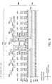
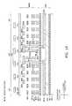
- FIG. 13is a schematic top view of a memory cell array layer 400 A of the nonvolatile semiconductor memory device according to the second embodiment of the invention.
- FIG. 14is an enlarged view of the portion C of FIG. 13 .
- FIG. 15is an enlarged view of the portion D of FIG. 13 .
- FIG. 16 and FIG. 17are views of FIG. 15 minus omitted portions.
- the first source line conductive layer 403 , a second source line conductive layer 414 , and the bit line conductive layer 405are omitted in FIG. 16 .
- FIG. 16is a schematic top view of a memory cell array layer 400 A of the nonvolatile semiconductor memory device according to the second embodiment of the invention.
- FIG. 14is an enlarged view of the portion C of FIG. 13 .
- FIG. 15is an enlarged view of the portion D of FIG. 13 .
- FIG. 16 and FIG. 17are views of FIG. 15 minus omitted portions.
- FIG. 18 to FIG. 22are cross-sectional views along lines VI-VI′ to X-X′ of FIG. 15 .
- the configuration of the memory cell array layer 400 A of the nonvolatile semiconductor memory device according to the second embodimentis different in comparison to that of the first embodiment.
- the memory cell array layer 400 Aincludes the first memory cell region 40 A and the connection region 40 C similar to those of the first embodiment. As illustrated in FIG. 13 , the memory cell array layer 400 A includes a second non-memory cell region 40 D different from that of the first embodiment. The memory cell array layer 400 A is also different from that of the first embodiment by further including a second memory cell region 40 E.
- the second non-memory cell region 40 Dhas a ladder configuration as viewed from above.
- the second non-memory cell region 40 Dincludes a pair of first regions 40 Da extending in the column direction and multiple second regions 40 Db extending in the row direction to connect the pair of the first regions 40 Da.
- the first region 40 Dais formed along an end portion extending in the column direction of the first memory cell region 40 A.
- the second regions 40 Dbare formed to include the connection region 40 C.
- the second memory cell region 40 Eis repeatedly formed between first memory cell regions 40 A adjacent in the row direction at a third pitch p 3 in the column direction. Restated, the second memory cell region 40 E is formed in a region enclosed by the first region 40 Da and the second region 40 Db of the second non-memory cell region 40 D.
- the memory cell array layer 400 Aincludes the second source line conductive layer 414 which is different than that of the first embodiment.
- the second source line conductive layer 414is formed in a layer above the bit line conductive layer 405 .
- the second source line conductive layer 414includes a source line connection plug layer 414 a on a lower face thereof.
- the source line connection plug layer 414 ais connected to an upper face of the first source line conductive layer 403 .
- the second source line conductive layer 414is formed in a layer above the bit line conductive layer 405 in the memory cell array layer 400 A. Therefore, different than those of the first embodiment, the bit line conductive layer 405 is formed also between the second source line conductive layer 414 and the upper interconnection layer 502 . The bit line conductive layer 405 is formed to straddle the connection region 40 C, the second memory cell region 40 E, and the second non-memory cell region 40 D.
- the memory cell array layer 400 Aincludes a bit line connection plug layer 405 b on a lower face of the bit line conductive layer 405 in the second memory cell region 40 E.
- the bit line connection plug layer 405 bis connected to a second contact layer 407 ′ of a memory unit Ut′ similar to those of the first memory cell region 40 A (referring to FIG. 18 ).
- the memory cell array layer 400 Aincludes a source line connection plug layer 404 b on a lower face of the second source line conductive layer 414 in the second memory cell region 40 E.
- the source line connection plug layer 404 bis connected to a first contact layer 406 ′ of the memory unit Ut′ (referring to FIG. 17 ).
- the nonvolatile semiconductor memory device according to the second embodimenthas the configuration recited above and therefore can provide effects similar to those of the first embodiment.
- the nonvolatile semiconductor memory device according to the second embodimentincludes the second memory cell region 40 E. Accordingly, the integration density of the memory cells MC of the nonvolatile semiconductor memory device according to the second embodiment can be increased even more than that of the first embodiment.
- FIG. 23is a schematic plan view illustrating a configuration of a nonvolatile semiconductor memory device according to the third embodiment of the invention.
- FIG. 24 , FIG. 25 , FIG. 26 , FIG. 27 , and FIG. 28are a cross-sectional view along line A-A′, a cross-sectional view along line B-B′, a cross-sectional view along line C-C′, a cross-sectional view along line D-D′, and a cross-sectional view along line E-E′ of FIG. 23 , respectively.
- FIG. 29is a schematic perspective view illustrating the configuration of a portion of the nonvolatile semiconductor memory device according to the third embodiment of the invention.
- the semiconductor substrate 110includes a memory cell region 120 and a peripheral circuit region 130 adjacent to the memory cell region 120 .
- a Z axisis a direction perpendicular to a major surface 111 of the semiconductor substrate 110 ;
- an X axisis a direction in a plane perpendicular to the Z axis and in which memory cells 210 , connected by common word lines WL as described below, are juxtaposed in the memory cell region 120 ;
- a Y axisis and a direction perpendicular to the Z axis and the X axis.
- the X axis and the Y axisare parallel to the major surface 111 .
- multiple memory cells 210are provided above the semiconductor substrate 110 of the memory cell region 120 and juxtaposed in the direction (Z-axis direction) perpendicular to the major surface 111 of the semiconductor substrate 110 .
- the memory cells 210are connected in series in the direction perpendicular to the major surface 111 to form a memory cell string 212 .
- the memory cell 210includes a semiconductor layer 250 provided on the major surface 111 of the semiconductor substrate 110 to extend in the direction perpendicular to the major surface 111 and an insulating layer 260 adjacent to the semiconductor layer 250 .
- a control gate 220is provided on the face of the insulating layer 260 on the side opposite to the semiconductor layer 250 in each memory cell 210 . In other words, the insulating layer 260 is provided between the semiconductor layer 250 and the control gate 220 .
- the control gates 220are multiply laminated in the direction perpendicular to the major surface 111 via not-illustrated insulating layers.
- the memory cells 210are connected in series in the direction perpendicular to the major surface 111 .
- control gate 220 layersare laminated in the direction (the Z-axis direction) perpendicular to the major surface 111 , the number of laminations is arbitrary. In other words, two or more layers of the control gates 220 may be multiply laminated.
- the semiconductor layer 250may include, for example, an n ⁇ -type SOI (Silicon On Insulator).
- the insulating layer 260may include, for example, three layers of laminated films such as SiO 2 —SiN—AlO.
- the control gate 220may include, for example, an n-type polysilicon. However, each of these materials is one example, and various modifications are possible.
- a drain-side selection gate line 370is provided on the uppermost portion of the memory cell string 212 .
- the uppermost portion of the semiconductor layer 250is connected to a bit line 380 .
- the drain-side selection gate line 370may include, for example, an n-type polysilicon.
- the bit line 380may include, for example, Cu. However, each of these materials is one example, and various modifications are possible.
- the bit line 380is omitted in FIG. 23 .
- a diffusion layer 331 in the memory cell regionis provided on the lowermost portion of the memory cell string 212 .
- the memory cells 210are multiply juxtaposed in the X-axis direction.
- a conductive layer 230which forms the control gates 220 of the memory cells 210 in the memory cell strings 212 juxtaposed at substantially the same distance from the major surface 111 as illustrated in FIG. 24 , is formed in the same layer.
- the conductive layer 230 which forms the control gates 220 of the memory cells 210extends in the X-axis direction and mutually connects the control gates 220 juxtaposed at substantially the same distance from the major surface 111 .
- the conductive layer 230includes a function as the word line WL.
- the word line WL including the conductive layer 230commonly connects, in the X-axis direction, the memory cells 210 formed at positions having substantially the same height from the major surface 111 of the semiconductor substrate 110 .
- the word lines WLwhich extend in the X-axis direction (the first direction) and include the conductive layer 230 forming the control gate 220 , are multiply disposed in the Y-axis direction (the second direction) in planes parallel to the major surface 111 of the semiconductor substrate 110 .
- the word line WLcommonly connects the memory cells 210 formed at positions having substantially the same height from the semiconductor substrate 110 .
- the memory cell strings 212are multiply disposed in the X-axis direction. Groups of the memory cell strings 212 commonly connected by common word lines WL and multiply disposed in the X-axis direction are multiply juxtaposed at different positions in the Y-axis direction.
- the conductive layer 230 forming the control gate 220also extends into the peripheral circuit region 130 .
- the word line WL connected to the memory cells 210extends into the peripheral circuit region 130 .
- a transfer gate transistor 310is provided on the major surface 111 of the semiconductor substrate 110 of the peripheral circuit region 130 .
- the transfer gate transistor 310includes a gate electrode 320 and diffusion layers 330 formed on either side of the gate electrode 320 .
- the gate electrode 320 of the transfer gate transistor 310is provided more proximal to the semiconductor substrate 110 side than is the conductive layer 230 forming the control gate 220 of the memory cells 210 .
- a first interconnection 350is an extension portion to the peripheral circuit region 130 of the conductive layer (a fifth conductive layer) 230 forming the control gate 220 of the memory cell 210 and passes above the gate electrode 320 .
- the first interconnection 350is a word line WL.
- the nonvolatile semiconductor memory device 10includes the semiconductor substrate 110 including the memory cell region 120 and the peripheral circuit region 130 provided adjacent to the memory cell region 120 .
- the nonvolatile semiconductor memory device 10further includes the memory cell string 212 , which is provided in the memory cell region 120 of the semiconductor substrate 110 and includes multiple memory cells 210 connected in series in the direction perpendicular to the major surface 111 of the semiconductor substrate 110 , and the transfer gate transistor 310 , which is provided on the peripheral circuit region 130 of the semiconductor substrate 110 .
- the nonvolatile semiconductor memory device 10further includes the first interconnection 350 which is formed by extending the conductive layer 230 forming the control gate 220 of the memory cell 210 into the peripheral circuit region 130 and passes above the gate electrode 320 of the transfer gate transistor 310 as viewed from the semiconductor substrate 110 .
- the conductive layer 230 forming the control gate 220 of the memory cell 210is a word line WL; and a portion of the word line WL forms the first interconnection 350 that passes above the gate electrode 320 of the transfer gate transistor 310 as viewed from the semiconductor substrate 110 .
- the conductive layer (a sixth conductive layer) 230 forming the control gate 220 of the memory cells 210that is, another portion of the word line WL, does not pass above the gate electrode 320 .
- the other portion of the word line WLextends into the peripheral circuit region 130 ; and the extension portion forms a second interconnection 352 that does not pass above the gate electrode 320 of the transfer gate transistor 310 .
- the spacing between the word lines WLcan be small in the portion above the gate electrode 320 of the transfer gate transistor 310 in the peripheral circuit region 130 .
- the spacing between the first interconnections 350 in the plane parallel to the major surface 111 of the semiconductor substrate 110 above the gate electrode 320can be smaller than the spacing between the conductive layers 230 in the plane parallel to the major surface 111 in the memory cell region 120 .
- the spacing between the second interconnection 352 and the first interconnection 350can be larger than the spacing between the first interconnections 350 that are above the same X axis as the gate electrode 320 but not above the gate electrode 320 .
- a contact electrode (inter-layer connection part) 360 and a contact electrode 361can be provided between the word lines WL, that is, the first interconnection 350 and the second interconnection 352 of regions not above the gate electrode 320 , and easily connect each of the laminated conductive layers 230 forming the control gate 220 of the laminated memory cell 210 to the peripheral circuit (for example, the transfer gate transistor 310 ).
- a contact electrode 361 connected to the diffusion layer 330 of the transfer gate transistor 310is provided between the laminated first interconnections 350 and the laminated second interconnections 352 .
- the contact electrode 361is connected to, for example, a portion of an upper layer electrode 390 .
- Another portion of the upper layer electrode 390is connected to a connection portion 392 provided on the lowermost word line WL of the laminated word lines WL (first interconnections 350 ) by another contact electrode (inter-layer connection part) 360 .
- the connection portion 392is formed by, for example, the conductive layer 230 protruding in the Y-axis direction.
- a portion of the upper layer electrode 390 connected to the diffusion layer 330 of the transfer gate transistor 310is connected to the connection portion 392 provided on the second lowermost word line WL (first interconnection 350 ) by the contact electrode 360 .
- a portion of the upper layer electrode 390 connected to the diffusion layer 330 of the transfer gate transistor 310is connected to the connection portion 392 provided on the third lowermost word line WL (first interconnection 350 ) by the contact electrode 360 .
- a portion of the upper layer electrode 390 connected to the diffusion layer 330 of the transfer gate transistor 310is connected to the connection portion 392 provided on the fourth lowermost (in this example, the uppermost) word line WL (first interconnection 350 ) by the contact electrode 360 .
- each of the laminated word lines WL(first interconnections 350 ) is conducted to the diffusion layer 330 .
- each of the laminated word lines WL (first interconnections 350 )is connected to the peripheral circuit.
- each of the laminated word lines WLincludes the connection portion 392 (a protruding portion formed by the conductive layer 230 protruding in the Y-axis direction) provided in different planar positions.
- the contact electrode 360 connecting to the upper layer electrode 390is connected to the connection portion 392 .
- the contact electrode 360may be connected to the second interconnection 352 as described below. In other words, the contact electrode 360 is connected to at least one of the first interconnection 350 and the second interconnection 352 .
- the nonvolatile semiconductor memory device 10further includes the second interconnection 352 , which is formed by the conductive layer 230 forming the control gate 220 of the memory cell 210 extending into the peripheral circuit region 130 and has a spacing to the first interconnection 350 in the plane parallel to the major surface 111 above the gate electrode 320 that is larger than a spacing between the first interconnections 350 in the plane above the gate electrode 320 , and an inter-layer connection part (the contact electrode 360 ), which is provided between the first interconnection 350 and the second interconnection 352 , extends in a direction non-parallel to the major surface 111 , and is connected to at least one of the first interconnection 350 and the second interconnection 352 .
- the second interconnection 352is formed by the conductive layer 230 forming the control gate 220 of the memory cell 210 extending into the peripheral circuit region 130 and has a spacing to the first interconnection 350 in the plane parallel to the major surface 111 above the gate electrode 320 that is larger than a spacing between the first interconnections 350
- word lines WLBy repeatedly disposing word lines WL having such a configuration in the Y-axis direction, it is possible to draw out the laminated word lines WL individually to the peripheral circuit region; and all of the word lines WL can be connected to the transfer gate transistor 310 in the nonvolatile semiconductor memory device 10 including laminated memory cells.
- the nonvolatile semiconductor memory device 10provides a nonvolatile semiconductor memory device having a high memory density that enables each laminated memory cell to connect to the peripheral circuit.
- the word lines WLcan detour around the contact electrode 360 to extend in the X-axis direction by curving the extension direction (changing the direction of the extension axis) of the word lines WL (the first interconnection 350 and the second interconnection 352 ), that is, causing the extension direction to form a curve in the Y-axis direction.
- the first interconnection 350which is one portion of the word line WL, passes above the gate electrode 320 of the transfer gate transistor 310 ; and the second interconnection 352 , which is another portion of the word line WL, does not pass above the gate electrode 320 .
- the word line WL(in this case, for example, the first interconnection 350 ), which is formed by the conductive layer 230 forming the control gate 220 of the memory cell 210 extending into the peripheral circuit region 130 , passes between inter-layer connection parts (in this case, for example, the contact electrodes 360 ) of the semiconductor substrate 110 .
- the contact electrode 360is disposed above neither the first interconnection 350 nor the second interconnection 352 which are word lines WL.
- the contact electrode 360is not necessarily disposed above all of the first interconnections 350 and the second interconnections 352 .
- the contact electrode 360may be disposed above a portion or more of the laminated first interconnections 350 and the laminated second interconnections 352 . Then, another portion of the first interconnections 350 and the second interconnections 352 may pass between the contact electrodes 360 .
- the nonvolatile semiconductor memory device 10includes: a semiconductor substrate 110 including a memory cell region 120 and a peripheral circuit region 130 provided adjacent to the memory cell region 120 ; a memory cell string 212 provided on the memory cell region 120 of the semiconductor substrate 110 and including multiple memory cells 210 connected in series in the direction perpendicular to the major surface 111 of the semiconductor substrate 110 ; the inter-layer connection part (the contact electrode 360 ) which is provided in the peripheral circuit region 130 of the semiconductor substrate 110 , extends in a direction non-parallel to the major surface 111 , and is electrically connected to the diffusion layer 330 of the transfer gate transistor 310 ; and the peripheral circuit region interconnection (the word line WL, that is, at least one of the first interconnection 350 and the second interconnection 352 ) which is formed by the conductive layer 230 forming the control gate 220 of the memory cell 210 , provided to extend in the first direction (the X-axis direction), protrudes in the second direction (for example
- the inter-layer connection part(the contact electrode 360 ) recited above is connected to the diffusion layer 330 of the transfer gate transistor 310 provided in the peripheral circuit region 130 of the semiconductor substrate 110 by the upper layer electrode 390 and the contact electrode 361 as described above.
- word lines WLBy repeatedly disposing word lines WL having such a configuration in the Y-axis direction, it is possible to draw out the laminated word lines WL individually to the peripheral circuit region; and all of the word lines WL can be connected to the transfer gate transistor 310 in the nonvolatile semiconductor memory device 10 including laminated memory cells.
- the nonvolatile semiconductor memory device 10provides a nonvolatile semiconductor memory device that enables each laminated memory cell to connect to the peripheral circuit.
- the contact electrode 361 connected to the transfer gate transistor 310is further connected to the not-illustrated row decoder, according to the structure of the nonvolatile semiconductor memory device 10 , the contact electrode 361 can be connected to the upper layer electrode 390 above the word line WL (more distal to the major surface 111 of the semiconductor substrate 110 than is the word line WL) as illustrated in FIG. 25 to FIG. 28 ; and the interconnection resistance can be reduced.
- the conductive layer 230 forming the control gate 220 in the memory cell region 120 of the nonvolatile semiconductor memory device 10includes a silicide portion 240 provided along the side face opposite to the control gate 220 side in the extension direction of the conductive layer 230 .
- the conductive layer 230 forming the control gate 220 in the peripheral circuit region 130includes the silicide portion 240 provided along both side faces in the extension direction (the X-axis direction) of the first interconnection 350 .
- the silicide portions 240may include, for example, NiSi x . Additionally, MoSi x , NbSi x , TaSi x , VSi x , WSi x , TiSi x , CoSi x , PdSi x , and the like also may be used.
- the silicide portion 240 in the memory cell region 120is provided on the conductive layer 230 forming the control gate 220 on the side face opposite to the control gate 220
- the silicide portion 240 in the peripheral circuit region 130is provided on the conductive layer 230 forming the control gate 220 on both side faces extending in the X-axis direction
- the silicide portion 240 of such a structurecan be formed by forming the memory cell 210 on the control gate 220 side of the conductive layer 230 , after which the insulating layer is provided to cover the memory cell 210 , the conductive layer 230 is patterned in a band configuration extending in the X-axis direction, and then the side faces of the conductive layer 230 are silicided.
- a nonvolatile semiconductor memory devicecan be realized having high reliability of the memory cell 210 , enabling manufacturing by simple methods, and providing word lines WL having low resistance.
- the silicide portion 240 in the memory cell region 120is not limited to the side face opposite to the control gate 220 of the conductive layer 230 , and may be provided on the same side face as the control gate 220 on the conductive layer 230 , and further, may be provided on both side faces of the conductive layer 230 . In such cases as well, the resistance of the word line WL formed by the conductive layer 230 forming the control gate 220 can be reduced.
- the conductive layer 230 forming the control gate 220 in the peripheral circuit region 130includes the silicide portion 240 on both side faces extending in the X-axis direction
- the silicide portion 240may be included on one of the side faces extending in the X-axis direction.
- the conductive layer 230 in the peripheral circuit region 130may be provided with the silicide portion 240 on the side face opposite to the control gate 220 of the conductive layer 230 forming the control gate 220 or on the same side face as the control gate 220 of the conductive layer 230 forming the control gate 220 . In such cases as well, the resistance of the word line WL formed by the conductive layer 230 forming the control gate 220 can be reduced.
- the peripheral circuit region interconnection (the word line WL, that is, at least one of the first interconnection 350 and the second interconnection 352 ) of the nonvolatile semiconductor memory device 10includes the connection portion 392 that protrudes in the second direction (for example, the Y-axis direction) non-parallel to the first direction (the X-axis direction) in the plane parallel to the major surface 111 of the semiconductor substrate 110 and has an independent configuration corresponding to each of the inter-layer connection parts (the contact electrodes 360 ) as illustrated in FIG. 29
- the configuration of the connection portion 392is arbitrary.
- FIG. 30is a schematic perspective view illustrating the configuration of a portion of another nonvolatile semiconductor memory device according to the third embodiment of the invention.
- connection portion 392 of the other nonvolatile semiconductor memory deviceis provided to extend along a side face of the peripheral circuit region interconnection (the word line WL, that is, at least one of the first interconnection 350 and the second interconnection 352 ) and has a continuous configuration extending in the X-axis direction while corresponding to the inter-layer connection part (the contact electrode 360 ).
- a nonvolatile semiconductor memory devicethat enables each laminated memory cell to connect to the peripheral circuit.
- FIG. 31is a schematic plan view illustrating a configuration of a nonvolatile semiconductor memory device according to a fourth embodiment of the invention.
- FIG. 32 , FIG. 33 , FIG. 34 , and FIG. 35are a cross-sectional view along line B-B′, a cross-sectional view along line C-C′, a cross-sectional view along line D-D′, and a cross-sectional view along line E-E′ of FIG. 31 , respectively.
- the spacing between the word lines WL(the first interconnections 350 ) is small in the portion above the gate electrode 320 of the transfer gate transistor 310 ; the spacing between the second interconnection 352 and the first interconnection 350 is larger than the spacing between the first interconnections 350 ; and the contact electrode (the inter-layer connection part) 360 is provided between the word lines WL, that is, between the first interconnection 350 and the second interconnection 352 , in a region not above the gate electrode 320 to connect the second interconnection 352 to the peripheral circuit.
- the nonvolatile semiconductor memory device 10has a structure in which the contact electrode (the inter-layer connection part) 360 connects to the first interconnection 350 and connects the first interconnection 350 to the peripheral circuit
- the nonvolatile semiconductor memory device 20has a structure in which the contact electrode (the inter-layer connection part) 360 connects to the second interconnection 352 and connects the second interconnection 352 to the peripheral circuit.
- the nonvolatile semiconductor memory device 20is similar to the nonvolatile semiconductor memory device 10 and a description is omitted.
- the contact electrode (the inter-layer connection part) 361 connected to the diffusion layer 330 of the transfer gate transistor 310is provided between the laminated first interconnections 350 and the laminated second interconnections 352 ; and the contact electrode 361 is connected to, for example, one portion of the upper layer electrode 390 . Then, another portion of the upper layer electrode 390 is connected to a connection portion 392 provided on the lowermost word line WL of the laminated word lines WL (the second interconnections 352 ) by another contact electrode (inter-layer connection part) 360 .
- one portion of the upper layer electrode 390 connected to the diffusion layer 330 of the transfer gate transistor 310is connected to a connection portion 392 provided on the second lowermost word line WL (second interconnection 352 ) by the contact electrode 360 .
- one portion of the upper layer electrode 390 connected to the diffusion layer 330 of the transfer gate transistor 310is connected to a connection portion 392 provided on the third lowermost word line WL (second interconnection 352 ) by the contact electrode 360 .
- one portion of the upper layer electrode 390 connected to the diffusion layer 330 of the transfer gate transistor 310is connected to a connection portion 392 provided on the fourth lowermost (in this example, the uppermost) word line WL (second interconnection 352 ) by the contact electrode 360 .
- each of the laminated word lines WL(the second interconnections 352 ) is conducted to the diffusion layer 330 .
- each of the laminated word lines WL(the second interconnections 352 ) is connected to the peripheral circuit.
- each of the laminated word lines WLincludes a connection portion 392 provided in a different planar position (a protruding portion formed by the conductive layer 230 protruding in, for example, the Y-axis direction); and a contact electrode 360 connected to an upper layer electrode 390 is connected to the connection portion 392 .
- connection portion 392 of the second interconnection 352 recited abovemay have the structures illustrated in FIG. 29 and FIG. 30 , that is, an independent configuration protruding in the second direction (for example, the Y-axis direction) non-parallel to the first direction (the X-axis direction) in the plane parallel to the major surface 111 of the semiconductor substrate 110 and corresponding to each of the inter-layer connection parts (the contact electrodes 360 ), and a continuous configuration extending along the side face of the word line WL (the second interconnection 352 ) and extending in the X-axis direction while corresponding to the inter-layer connection part (the contact electrode 360 ).
- the nonvolatile semiconductor memory device 20can provide a nonvolatile semiconductor memory device that enables each laminated memory cell to connect to the peripheral circuit.
- FIG. 36is a schematic plan view illustrating a configuration of a nonvolatile semiconductor memory device according to a fifth embodiment of the invention.
- the spacing between the word lines WL(the first interconnections 350 ) is small and the spacing between the second interconnection 352 and the first interconnection 350 is larger than the spacing between the first interconnections 350 in a portion above the gate electrode 320 of the transfer gate transistor 310 .
- the inter-layer connection part(the contact electrode 360 ) can be provided between the first interconnection 350 and the second interconnection 352 in a region that is above the same X axis as the gate electrode 320 but not above the gate electrode 320 .
- the contact electrode 360is connected to the connection portion 392 of the second interconnection 352 and the upper layer electrode 390 .
- the upper layer electrode 390is connected to the diffusion layer 330 of the transfer gate transistor 310 by another contact electrode 361 .
- the second interconnection 352is connected to the peripheral circuit (the transfer gate transistor 310 ).
- each of the laminated second interconnections 352include a connection portion 392 (a protruding portion formed by the conductive layer 230 protruding in, for example, the Y-axis direction) provided in different planar positions.
- the contact electrode 360 connected to the upper layer electrode 390is connected to the connection portion 392 ; and all of the second interconnections 352 laminated in each layer are connected to the peripheral circuit.
- the spacing between the first interconnections 350is large, and the spacing between the second interconnection 352 and the first interconnection 350 is smaller than the spacing between the first interconnections 350 .
- the inter-layer connection part(the contact electrode 360 ) is provided between the first interconnections 350 having a large spacing therebetween.
- the contact electrode 360is connected to the connection portion 392 of the first interconnection 350 and the upper layer electrode 390 .
- the upper layer electrode 390is connected to the diffusion layer 330 of the transfer gate transistor 310 by another contact electrode 361 . Thereby, each of the laminated first interconnections 350 is connected to the peripheral circuit (the transfer gate transistor 310 ).
- each of the laminated first interconnections 350includes a connection portion 392 (a protruding portion formed by the conductive layer 230 protruding in, for example, the Y-axis direction) provided in different planar positions.
- the contact electrode 360 connected to the upper layer electrode 390is connected to the connection portion 392 . All of the first interconnections 350 in each laminated layer are connected to the peripheral circuit.
- the nonvolatile semiconductor memory device 30includes a portion in which the spacing between the first interconnections 350 is small and the spacing between the first interconnection 350 and the second interconnection 352 is large.
- the inter-layer connection part(the contact electrode 360 ) is provided between the first interconnection 350 and the second interconnection 352 .
- the inter-layer connection part(the contact electrode 360 ) is provided between the first interconnections 350 in another portion, disposed in the X-axis direction of the first interconnection 350 having the portion in which the mutual spacing is small, which has a large spacing between the first interconnections 350 .
- the inter-layer connection partconnects each of the connected first interconnections 350 and second interconnections 352 to the peripheral circuit.
- the portion recited above in which the spacing between the first interconnections 350 is smallpasses above the gate electrode 320 of the transfer gate transistor 310 .
- each of the laminated first interconnections 350 and second interconnections 352can be connected to the peripheral circuit.
- the nonvolatile semiconductor memory device 30 according to this embodimentcan provide a nonvolatile semiconductor memory device that enables each laminated memory cell to connect to the peripheral circuit.
- FIG. 37is a schematic plan view illustrating the configuration of another nonvolatile semiconductor memory device according to the fifth embodiment of the invention.
- the spacing between the word lines WL(the first interconnections 350 ) is small, and the spacing between the second interconnection 352 and the first interconnection 350 is larger than the spacing between the first interconnections 350 in a portion above the gate electrode 320 of the transfer gate transistor 310 .
- the inter-layer connection part(the contact electrode 360 ) is provided between the first interconnection 350 and the second interconnection 352 in a region on the same X axis of the gate electrode 320 other than above the gate electrode 320 .
- the contact electrode 360is connected to the connection portion 392 of the first interconnection 350 and the upper layer electrode 390 .
- the upper layer electrode 390is connected to the diffusion layer 330 of the transfer gate transistor 310 by another contact electrode 361 .
- each of the laminated first interconnections 350is connected to the peripheral circuit (the transfer gate transistor 310 ).
- each of the laminated first interconnections 350includes the connection portion 392 (the protruding portion formed by the conductive layer 230 protruding in, for example, the Y-axis direction) provided in different planar positions.
- the contact electrode 360 connected to the upper layer electrode 390is connected to the connection portion 392 . All of the first interconnections 350 of each laminated layer are connected to the peripheral circuit.
- the spacing between the second interconnection 352 and another interconnection 353is large on the peripheral region side of the transfer gate transistor 310 in the X-axis direction (the direction opposite to the memory cell region 120 as viewed from the transfer gate transistor 310 ).
- the inter-layer connection part(the contact electrode 360 ) is provided in the portion in which the spacing to the other interconnection 353 is large.
- the contact electrode 360is connected to the connection portion 392 of the second interconnection 352 and the upper layer electrode 390 .
- the upper layer electrode 390is connected to the diffusion layer 330 of the transfer gate transistor 310 by another contact electrode 361 .
- each of the laminated second interconnections 352is connected to the peripheral circuit (the transfer gate transistor 310 ).
- each of the laminated second interconnections 352include the connection portion 392 (the protruding portion formed by the conductive layer 230 protruding in, for example, the Y-axis direction) provided in different planar positions.
- the contact electrode 360 connected to the upper layer electrode 390is connected to the connection portion 392 . All of the second interconnections 352 in each laminated layer are connected to the peripheral circuit.
- the nonvolatile semiconductor memory device 31includes a portion in which the spacing between the first interconnection 350 and the second interconnection 352 is large.
- the inter-layer connection partis provided between the first interconnection 350 and the second interconnection 352 of this portion.
- the inter-layer connection partis provided in a portion in which the spacing between the second interconnection 352 and the other interconnection 353 is large.
- the inter-layer connection partconnects each of the connected first interconnection 350 and second interconnection 352 to the peripheral circuit.
- the portion recited above in which the spacing between the first interconnection 350 and the second interconnection 352 is largeis formed by arranging the portion in which the spacing between the first interconnections 350 is small; and the portion in which the spacing between the first interconnections 350 is small passes above the gate electrode 320 of the transfer gate transistor 310 .
- each of the laminated first interconnections 350 and second interconnections 352can be connected to the peripheral circuit.
- the nonvolatile semiconductor memory device 31 according to this embodimentcan provide a nonvolatile semiconductor memory device that enables each laminated memory cell to connect to the peripheral circuit.
- FIG. 38is a schematic plan view illustrating the configuration of another nonvolatile semiconductor memory device according to the fifth embodiment of the invention.
- first interconnections 350pass through the portion above the gate electrode 320 of the transfer gate transistor 310 in the nonvolatile semiconductor memory device 30 illustrated in FIG. 36
- four first interconnections 350pass through the portion above the gate electrode 320 in the nonvolatile semiconductor memory device 32 .
- the number of word lines WL (first interconnections 350 ) passing through the portion above the gate electrode 320 in this embodimentis arbitrary.
- the spacing between the word lines WL(the first interconnections 350 ) is small, and the spacing between the second interconnection 352 and the first interconnection 350 is larger than the spacing between the first interconnections 350 .
- the inter-layer connection part(the contact electrode 360 ) can be provided between the first interconnection 350 and the second interconnection 352 in the region that is above the same X axis of the gate electrode 320 but not above the gate electrode 320 .
- the contact electrode 360is connected to the connection portions 392 of two first interconnections 350 on the second interconnection 352 side and the upper layer electrode 390 .
- the upper layer electrode 390is connected to the diffusion layer 330 of the transfer gate transistor 310 by another contact electrode 361 .
- each of the laminated conductive layers 230 forming the two first interconnections 350 on the second interconnection 352 sideare connected to the peripheral circuit (the transfer gate transistor 310 ).
- each of the laminated first interconnections 350includes the connection portion 392 (the protruding portion formed by the conductive layer 230 protruding in, for example, the Y-axis direction) provided at different planar positions.
- the contact electrode 360 connected to the upper layer electrode 390is connected to the connection portion 392 . All of the first interconnections 350 in each laminated layer are connected to the peripheral circuit.
- the spacing between the two first interconnections 350 on the distal side as viewed from the second interconnection 352is large.
- the contact electrode (the inter-layer connection part) 360is provided between the first interconnections 350 having the large mutual spacing.
- the contact electrode 360is connected to the upper layer electrode 390 and the connection portion 392 of the two first interconnections 350 on the distal side as viewed from the second interconnection 352 .
- the upper layer electrode 390is connected to the diffusion layer 330 of the transfer gate transistor 310 by the other contact electrode 361 .
- each of the laminated conductive layers 230 forming the two first interconnections 350 on the distal side as viewed from the second interconnection 352is connected to the peripheral circuit (the transfer gate transistor 310 ).
- each of the laminated first interconnections 350includes the connection portion 392 (the protruding portion formed by the conductive layer 230 protruding in, for example, the Y-axis direction) provided in different planar positions.
- the contact electrode 360 connected to the upper layer electrode 390is connected to the connection portion 392 . All of the first interconnections 350 of each laminated layer are connected to the peripheral circuit.
- the nonvolatile semiconductor memory device 32includes the portion in which the spacing between the first interconnections 350 is small and the portion adjacent thereto in the Y-axis direction in which spacing between the first interconnection 350 and the second interconnection 352 is large.
- the inter-layer connection partis provided between the first interconnection 350 and the second interconnection 352 .
- the inter-layer connection partconnects the second interconnection 352 to the peripheral circuit.
- the inter-layer connection partis provided between the first interconnections 350 in a portion at a position not on the X axis of the gate electrode 320 of the transfer gate transistor 310 in which the spacing between the first interconnections 350 is large.
- the inter-layer connection partconnects the first interconnection 350 to the peripheral circuit.
- each of the laminated first interconnections 350can be connected to the peripheral circuit.
- the nonvolatile semiconductor memory device 32 according to this embodimentcan provide a nonvolatile semiconductor memory device that enables each laminated memory cell to connect to the peripheral circuit.
- FIG. 39is a schematic plan view illustrating the configuration of another nonvolatile semiconductor memory device according to the fifth embodiment of the invention.
- the spacing between the word lines WL(the first interconnections 350 ) is small and the spacing between the second interconnection 352 and the first interconnection 350 is larger than the spacing between the first interconnections 350 in the portion above the gate electrode 320 of the transfer gate transistor 310 .
- the inter-layer connection part(the contact electrode 360 ) is provided between the first interconnection 350 and the second interconnection 352 in the region that is above the same X axis of the gate electrode 320 but not above the gate electrode 320 .
- the contact electrode 360is connected to the connection portions 392 of the two first interconnections 350 on the second interconnection 352 side and the upper layer electrode 390 .
- the upper layer electrode 390is connected to the diffusion layer 330 of the transfer gate transistor 310 by the other contact electrode 361 .
- each of the laminated conductive layers 230 forming the two first interconnections 350 on the second interconnection 352 sideare connected to the peripheral circuit (the transfer gate transistor 310 ).
- the spacing between the two first interconnections 350 on the distal side as viewed from the second interconnection 352is large.
- the contact electrode (the inter-layer connection part) 360is provided between the first interconnections 350 in which the mutual spacing is large.
- the contact electrode 360is connected to the upper layer electrode 390 and the connection portions 392 of the two first interconnections 350 on the distal side as viewed from the second interconnection 352 .
- the upper layer electrode 390is connected to the diffusion layer 330 of the transfer gate transistor 310 by the other contact electrode 361 .
- each of the laminated conductive layers 230 forming the two first interconnections 350 on the distal side as viewed from the second interconnection 352are connected to the peripheral circuit (the transfer gate transistor 310 ).
- Another contact electrode 360is provided between the first interconnection 350 and the second interconnection 352 at a different position in the Y direction than the contact electrode 360 connecting the peripheral circuit to the two first interconnections 350 on the distal side as viewed from the second interconnection 352 recited above.
- the other contact electrode 360is connected to the second interconnection 352 .
- each of the laminated second interconnections 352is connected to the peripheral circuit.
- each of the laminated first interconnections 350 and second interconnections 352can be connected to the peripheral circuit.
- the nonvolatile semiconductor memory device 33can be provided as a nonvolatile semiconductor memory device that enables each laminated memory cell to connect to the peripheral circuit.
- the nonvolatile semiconductor memory devicesinclude a distinctive layout of the word lines WL above the transfer gate transistor 310 in regard to the structure of a laminated nonvolatile semiconductor memory device. Thereby, it is possible to draw out the laminated word lines WL individually to the peripheral circuit region; and all of the word lines WL can be connected to the transfer gate transistor 310 in a nonvolatile semiconductor memory device including laminated memory cells.
- each word line WLis connected to an individual transfer gate transistor corresponding to each word line WL.
- FIG. 40is a schematic plan view illustrating the configuration of a nonvolatile semiconductor memory device according to a sixth embodiment of the invention.
- This embodimentcan also be applied to the third, fourth and fifth embodiments.
- a portion of the word lines WLis connected to the transfer gate transistor 310 illustrated in FIG. 40 , and another portion of the word lines WL is connected to, for example, another not-illustrated transfer gate transistor disposed in the positive direction of the X axis from the transfer gate transistor 310 .
- each of the word lines WLcan be connected to another transfer gate transistor corresponding to each word line WL.
- nonvolatile semiconductor memory devicesthat can be obtained by an appropriate design modification by one skilled in the art based on the nonvolatile semiconductor memory devices described above as embodiments of the invention also are within the scope of the invention to the extent that the purport of the invention is included.
Landscapes
- Engineering & Computer Science (AREA)
- Microelectronics & Electronic Packaging (AREA)
- Non-Volatile Memory (AREA)
- Semiconductor Memories (AREA)
Abstract
Description
Claims (7)
Applications Claiming Priority (4)
| Application Number | Priority Date | Filing Date | Title |
|---|---|---|---|
| JP2008191762AJP2010034109A (en) | 2008-07-25 | 2008-07-25 | Nonvolatile semiconductor memory device |
| JP2008-191762 | 2008-07-25 | ||
| JP2008283547AJP2010114153A (en) | 2008-11-04 | 2008-11-04 | Nonvolatile semiconductor memory device |
| JP2008-283547 | 2008-11-04 |
Publications (2)
| Publication Number | Publication Date |
|---|---|
| US20100020608A1 US20100020608A1 (en) | 2010-01-28 |
| US8044448B2true US8044448B2 (en) | 2011-10-25 |
Family
ID=41568526
Family Applications (1)
| Application Number | Title | Priority Date | Filing Date |
|---|---|---|---|
| US12/508,904Active2030-01-01US8044448B2 (en) | 2008-07-25 | 2009-07-24 | Nonvolatile semiconductor memory device |
Country Status (1)
| Country | Link |
|---|---|
| US (1) | US8044448B2 (en) |
Cited By (184)
| Publication number | Priority date | Publication date | Assignee | Title |
|---|---|---|---|---|
| US20100214838A1 (en)* | 2009-02-24 | 2010-08-26 | Kabushiki Kaisha Toshiba | Non-volatile semiconductor storage device |
| US20110002178A1 (en)* | 2009-07-06 | 2011-01-06 | Sung-Min Hwang | Vertical non-volatile memory device, method of fabricating the same device, and electric-electronic system having the same device |
| US8476708B2 (en) | 2011-01-13 | 2013-07-02 | Kabushiki Kaisha Toshiba | Semiconductor memory device having a circuit formed on a single crystal semiconductor layer with varied germanium concentration |
| US9299393B2 (en) | 2010-09-14 | 2016-03-29 | Semiconductor Energy Laboratory Co., Ltd. | Memory device and semiconductor device |
| US20160211267A1 (en)* | 2011-09-21 | 2016-07-21 | Semiconductor Energy Laboratory Co., Ltd. | Semiconductor storage device |
| US9431415B2 (en) | 2013-11-08 | 2016-08-30 | Samsung Electronics Co., Ltd. | Semiconductor device with vertical memory |
| US9508738B2 (en) | 2014-05-12 | 2016-11-29 | Samsung Electronics Co., Ltd. | Semiconductor devices |
| US9558945B2 (en) | 2014-09-12 | 2017-01-31 | Kabushiki Kaisha Toshiba | Semiconductor memory device with electrode connecting to circuit chip through memory array chip |
| US9601178B2 (en) | 2011-01-26 | 2017-03-21 | Semiconductor Energy Laboratory Co., Ltd. | Memory device and semiconductor device |
| US9608001B2 (en) | 2015-03-13 | 2017-03-28 | Kabushiki Kaisha Toshiba | Semiconductor memory device |
| TWI581608B (en)* | 2012-06-27 | 2017-05-01 | Toshiba Kk | Semiconductor memory device |
| US9680029B2 (en) | 2010-10-29 | 2017-06-13 | Semiconductor Energy Laboratory Co., Ltd. | Semiconductor memory device |
| US9876029B2 (en)* | 2016-03-22 | 2018-01-23 | Toshiba Memory Corporation | Semiconductor memory device |
| US9941009B2 (en) | 2016-05-16 | 2018-04-10 | Samsung Electronics Co., Ltd. | Memory device having vertical structure and memory system including the same |
| US10224279B2 (en) | 2013-03-15 | 2019-03-05 | Monolithic 3D Inc. | Semiconductor device and structure |
| US10325651B2 (en) | 2013-03-11 | 2019-06-18 | Monolithic 3D Inc. | 3D semiconductor device with stacked memory |
| US10354995B2 (en) | 2009-10-12 | 2019-07-16 | Monolithic 3D Inc. | Semiconductor memory device and structure |
| US20190237475A1 (en)* | 2018-01-31 | 2019-08-01 | Samsung Electronics Co., Ltd. | Three-dimensional semiconductor device |
| US10381328B2 (en) | 2015-04-19 | 2019-08-13 | Monolithic 3D Inc. | Semiconductor device and structure |
| US10388568B2 (en) | 2011-06-28 | 2019-08-20 | Monolithic 3D Inc. | 3D semiconductor device and system |
| US10388863B2 (en) | 2009-10-12 | 2019-08-20 | Monolithic 3D Inc. | 3D memory device and structure |
| US10418369B2 (en) | 2015-10-24 | 2019-09-17 | Monolithic 3D Inc. | Multi-level semiconductor memory device and structure |
| US20190287985A1 (en)* | 2018-03-16 | 2019-09-19 | Toshiba Memory Corporation | Memory device |
| US10497713B2 (en) | 2010-11-18 | 2019-12-03 | Monolithic 3D Inc. | 3D semiconductor memory device and structure |
| US10515981B2 (en) | 2015-09-21 | 2019-12-24 | Monolithic 3D Inc. | Multilevel semiconductor device and structure with memory |
| US10522225B1 (en) | 2015-10-02 | 2019-12-31 | Monolithic 3D Inc. | Semiconductor device with non-volatile memory |
| US10600888B2 (en) | 2012-04-09 | 2020-03-24 | Monolithic 3D Inc. | 3D semiconductor device |
| US10600657B2 (en) | 2012-12-29 | 2020-03-24 | Monolithic 3D Inc | 3D semiconductor device and structure |
| US10651054B2 (en) | 2012-12-29 | 2020-05-12 | Monolithic 3D Inc. | 3D semiconductor device and structure |
| US10679977B2 (en) | 2010-10-13 | 2020-06-09 | Monolithic 3D Inc. | 3D microdisplay device and structure |
| US10825779B2 (en) | 2015-04-19 | 2020-11-03 | Monolithic 3D Inc. | 3D semiconductor device and structure |
| US10833108B2 (en) | 2010-10-13 | 2020-11-10 | Monolithic 3D Inc. | 3D microdisplay device and structure |
| US10840239B2 (en) | 2014-08-26 | 2020-11-17 | Monolithic 3D Inc. | 3D semiconductor device and structure |
| US10847540B2 (en) | 2015-10-24 | 2020-11-24 | Monolithic 3D Inc. | 3D semiconductor memory device and structure |
| US10892016B1 (en) | 2019-04-08 | 2021-01-12 | Monolithic 3D Inc. | 3D memory semiconductor devices and structures |
| US10892269B2 (en) | 2014-09-12 | 2021-01-12 | Toshiba Memory Corporation | Semiconductor memory device having a bonded circuit chip including a solid state drive controller connected to a control circuit |
| US10892169B2 (en) | 2012-12-29 | 2021-01-12 | Monolithic 3D Inc. | 3D semiconductor device and structure |
| US10896931B1 (en) | 2010-10-11 | 2021-01-19 | Monolithic 3D Inc. | 3D semiconductor device and structure |
| US10903089B1 (en) | 2012-12-29 | 2021-01-26 | Monolithic 3D Inc. | 3D semiconductor device and structure |
| US10910364B2 (en) | 2009-10-12 | 2021-02-02 | Monolitaic 3D Inc. | 3D semiconductor device |
| US10943934B2 (en) | 2010-10-13 | 2021-03-09 | Monolithic 3D Inc. | Multilevel semiconductor device and structure |
| US10964807B2 (en) | 2013-03-11 | 2021-03-30 | Monolithic 3D Inc. | 3D semiconductor device with memory |
| US10978501B1 (en) | 2010-10-13 | 2021-04-13 | Monolithic 3D Inc. | Multilevel semiconductor device and structure with waveguides |
| US10998374B1 (en) | 2010-10-13 | 2021-05-04 | Monolithic 3D Inc. | Multilevel semiconductor device and structure |
| US11004694B1 (en) | 2012-12-29 | 2021-05-11 | Monolithic 3D Inc. | 3D semiconductor device and structure |
| US11004719B1 (en) | 2010-11-18 | 2021-05-11 | Monolithic 3D Inc. | Methods for producing a 3D semiconductor memory device and structure |
| US11011507B1 (en) | 2015-04-19 | 2021-05-18 | Monolithic 3D Inc. | 3D semiconductor device and structure |
| US11018191B1 (en) | 2010-10-11 | 2021-05-25 | Monolithic 3D Inc. | 3D semiconductor device and structure |
| US11018116B2 (en) | 2012-12-22 | 2021-05-25 | Monolithic 3D Inc. | Method to form a 3D semiconductor device and structure |
| US11018156B2 (en) | 2019-04-08 | 2021-05-25 | Monolithic 3D Inc. | 3D memory semiconductor devices and structures |
| US11018042B1 (en) | 2010-11-18 | 2021-05-25 | Monolithic 3D Inc. | 3D semiconductor memory device and structure |
| US11018133B2 (en) | 2009-10-12 | 2021-05-25 | Monolithic 3D Inc. | 3D integrated circuit |
| US11024673B1 (en) | 2010-10-11 | 2021-06-01 | Monolithic 3D Inc. | 3D semiconductor device and structure |
| US11031394B1 (en) | 2014-01-28 | 2021-06-08 | Monolithic 3D Inc. | 3D semiconductor device and structure |
| US11031275B2 (en) | 2010-11-18 | 2021-06-08 | Monolithic 3D Inc. | 3D semiconductor device and structure with memory |
| US11030371B2 (en) | 2013-04-15 | 2021-06-08 | Monolithic 3D Inc. | Automation for monolithic 3D devices |
| US11043523B1 (en) | 2010-10-13 | 2021-06-22 | Monolithic 3D Inc. | Multilevel semiconductor device and structure with image sensors |
| US20210202496A1 (en)* | 2019-12-31 | 2021-07-01 | Samsung Electronics Co., Ltd. | Integrated circuit device |
| US11056468B1 (en) | 2015-04-19 | 2021-07-06 | Monolithic 3D Inc. | 3D semiconductor device and structure |
| US11063071B1 (en) | 2010-10-13 | 2021-07-13 | Monolithic 3D Inc. | Multilevel semiconductor device and structure with waveguides |
| US11063024B1 (en) | 2012-12-22 | 2021-07-13 | Monlithic 3D Inc. | Method to form a 3D semiconductor device and structure |
| US11087995B1 (en) | 2012-12-29 | 2021-08-10 | Monolithic 3D Inc. | 3D semiconductor device and structure |
| US11088050B2 (en) | 2012-04-09 | 2021-08-10 | Monolithic 3D Inc. | 3D semiconductor device with isolation layers |
| US11088130B2 (en) | 2014-01-28 | 2021-08-10 | Monolithic 3D Inc. | 3D semiconductor device and structure |
| US11094576B1 (en) | 2010-11-18 | 2021-08-17 | Monolithic 3D Inc. | Methods for producing a 3D semiconductor memory device and structure |
| US11107808B1 (en) | 2014-01-28 | 2021-08-31 | Monolithic 3D Inc. | 3D semiconductor device and structure |
| US11107721B2 (en) | 2010-11-18 | 2021-08-31 | Monolithic 3D Inc. | 3D semiconductor device and structure with NAND logic |
| US11114464B2 (en) | 2015-10-24 | 2021-09-07 | Monolithic 3D Inc. | 3D semiconductor device and structure |
| US11114427B2 (en) | 2015-11-07 | 2021-09-07 | Monolithic 3D Inc. | 3D semiconductor processor and memory device and structure |
| US11121021B2 (en) | 2010-11-18 | 2021-09-14 | Monolithic 3D Inc. | 3D semiconductor device and structure |
| US11133344B2 (en) | 2010-10-13 | 2021-09-28 | Monolithic 3D Inc. | Multilevel semiconductor device and structure with image sensors |
| US11158674B2 (en) | 2010-10-11 | 2021-10-26 | Monolithic 3D Inc. | Method to produce a 3D semiconductor device and structure |
| US11158652B1 (en) | 2019-04-08 | 2021-10-26 | Monolithic 3D Inc. | 3D memory semiconductor devices and structures |
| US11163112B2 (en) | 2010-10-13 | 2021-11-02 | Monolithic 3D Inc. | Multilevel semiconductor device and structure with electromagnetic modulators |
| US11164898B2 (en) | 2010-10-13 | 2021-11-02 | Monolithic 3D Inc. | Multilevel semiconductor device and structure |
| US11164811B2 (en) | 2012-04-09 | 2021-11-02 | Monolithic 3D Inc. | 3D semiconductor device with isolation layers and oxide-to-oxide bonding |
| US11164770B1 (en) | 2010-11-18 | 2021-11-02 | Monolithic 3D Inc. | Method for producing a 3D semiconductor memory device and structure |
| US11177140B2 (en) | 2012-12-29 | 2021-11-16 | Monolithic 3D Inc. | 3D semiconductor device and structure |
| US11211279B2 (en) | 2010-11-18 | 2021-12-28 | Monolithic 3D Inc. | Method for processing a 3D integrated circuit and structure |
| US11217565B2 (en) | 2012-12-22 | 2022-01-04 | Monolithic 3D Inc. | Method to form a 3D semiconductor device and structure |
| US11227897B2 (en) | 2010-10-11 | 2022-01-18 | Monolithic 3D Inc. | Method for producing a 3D semiconductor memory device and structure |
| US11251149B2 (en) | 2016-10-10 | 2022-02-15 | Monolithic 3D Inc. | 3D memory device and structure |
| US11257867B1 (en) | 2010-10-11 | 2022-02-22 | Monolithic 3D Inc. | 3D semiconductor device and structure with oxide bonds |
| US11270055B1 (en) | 2013-04-15 | 2022-03-08 | Monolithic 3D Inc. | Automation for monolithic 3D devices |
| US11282827B2 (en) | 2019-10-16 | 2022-03-22 | Samsung Electronics Co., Ltd. | Nonvolatile memory device having stacked structure with spaced apart conductive layers |
| US11296115B1 (en) | 2015-10-24 | 2022-04-05 | Monolithic 3D Inc. | 3D semiconductor device and structure |
| US11296106B2 (en) | 2019-04-08 | 2022-04-05 | Monolithic 3D Inc. | 3D memory semiconductor devices and structures |
| US11309292B2 (en) | 2012-12-22 | 2022-04-19 | Monolithic 3D Inc. | 3D semiconductor device and structure with metal layers |
| US11315980B1 (en) | 2010-10-11 | 2022-04-26 | Monolithic 3D Inc. | 3D semiconductor device and structure with transistors |
| US11327227B2 (en) | 2010-10-13 | 2022-05-10 | Monolithic 3D Inc. | Multilevel semiconductor device and structure with electromagnetic modulators |
| US11329059B1 (en) | 2016-10-10 | 2022-05-10 | Monolithic 3D Inc. | 3D memory devices and structures with thinned single crystal substrates |
| US11341309B1 (en) | 2013-04-15 | 2022-05-24 | Monolithic 3D Inc. | Automation for monolithic 3D devices |
| US11355380B2 (en) | 2010-11-18 | 2022-06-07 | Monolithic 3D Inc. | Methods for producing 3D semiconductor memory device and structure utilizing alignment marks |
| US11355381B2 (en) | 2010-11-18 | 2022-06-07 | Monolithic 3D Inc. | 3D semiconductor memory device and structure |
| US11374118B2 (en) | 2009-10-12 | 2022-06-28 | Monolithic 3D Inc. | Method to form a 3D integrated circuit |
| US11398569B2 (en) | 2013-03-12 | 2022-07-26 | Monolithic 3D Inc. | 3D semiconductor device and structure |
| US11404466B2 (en) | 2010-10-13 | 2022-08-02 | Monolithic 3D Inc. | Multilevel semiconductor device and structure with image sensors |
| US11410912B2 (en) | 2012-04-09 | 2022-08-09 | Monolithic 3D Inc. | 3D semiconductor device with vias and isolation layers |
| US11430668B2 (en) | 2012-12-29 | 2022-08-30 | Monolithic 3D Inc. | 3D semiconductor device and structure with bonding |
| US11430806B2 (en) | 2019-10-16 | 2022-08-30 | Samsung Electronics Co., Ltd. | Nonvolatile memory device |
| US11430667B2 (en) | 2012-12-29 | 2022-08-30 | Monolithic 3D Inc. | 3D semiconductor device and structure with bonding |
| US11437368B2 (en) | 2010-10-13 | 2022-09-06 | Monolithic 3D Inc. | Multilevel semiconductor device and structure with oxide bonding |
| US11443971B2 (en) | 2010-11-18 | 2022-09-13 | Monolithic 3D Inc. | 3D semiconductor device and structure with memory |
| US11469271B2 (en) | 2010-10-11 | 2022-10-11 | Monolithic 3D Inc. | Method to produce 3D semiconductor devices and structures with memory |
| US11476181B1 (en) | 2012-04-09 | 2022-10-18 | Monolithic 3D Inc. | 3D semiconductor device and structure with metal layers |
| US11482438B2 (en) | 2010-11-18 | 2022-10-25 | Monolithic 3D Inc. | Methods for producing a 3D semiconductor memory device and structure |
| US11482439B2 (en) | 2010-11-18 | 2022-10-25 | Monolithic 3D Inc. | Methods for producing a 3D semiconductor memory device comprising charge trap junction-less transistors |
| US11482440B2 (en) | 2010-12-16 | 2022-10-25 | Monolithic 3D Inc. | 3D semiconductor device and structure with a built-in test circuit for repairing faulty circuits |
| US11487928B2 (en) | 2013-04-15 | 2022-11-01 | Monolithic 3D Inc. | Automation for monolithic 3D devices |
| US11495484B2 (en) | 2010-11-18 | 2022-11-08 | Monolithic 3D Inc. | 3D semiconductor devices and structures with at least two single-crystal layers |
| US11508605B2 (en) | 2010-11-18 | 2022-11-22 | Monolithic 3D Inc. | 3D semiconductor memory device and structure |
| US11521888B2 (en) | 2010-11-18 | 2022-12-06 | Monolithic 3D Inc. | 3D semiconductor device and structure with high-k metal gate transistors |
| US11569117B2 (en) | 2010-11-18 | 2023-01-31 | Monolithic 3D Inc. | 3D semiconductor device and structure with single-crystal layers |
| US11574109B1 (en) | 2013-04-15 | 2023-02-07 | Monolithic 3D Inc | Automation methods for 3D integrated circuits and devices |
| US11594473B2 (en) | 2012-04-09 | 2023-02-28 | Monolithic 3D Inc. | 3D semiconductor device and structure with metal layers and a connective path |
| US11600667B1 (en) | 2010-10-11 | 2023-03-07 | Monolithic 3D Inc. | Method to produce 3D semiconductor devices and structures with memory |
| US11605663B2 (en) | 2010-10-13 | 2023-03-14 | Monolithic 3D Inc. | Multilevel semiconductor device and structure with image sensors and wafer bonding |
| US11610802B2 (en) | 2010-11-18 | 2023-03-21 | Monolithic 3D Inc. | Method for producing a 3D semiconductor device and structure with single crystal transistors and metal gate electrodes |
| US11615977B2 (en) | 2010-11-18 | 2023-03-28 | Monolithic 3D Inc. | 3D semiconductor memory device and structure |
| US11616004B1 (en) | 2012-04-09 | 2023-03-28 | Monolithic 3D Inc. | 3D semiconductor device and structure with metal layers and a connective path |
| US11694922B2 (en) | 2010-10-13 | 2023-07-04 | Monolithic 3D Inc. | Multilevel semiconductor device and structure with oxide bonding |
| US11694944B1 (en) | 2012-04-09 | 2023-07-04 | Monolithic 3D Inc. | 3D semiconductor device and structure with metal layers and a connective path |
| US11711928B2 (en) | 2016-10-10 | 2023-07-25 | Monolithic 3D Inc. | 3D memory devices and structures with control circuits |
| US11720736B2 (en) | 2013-04-15 | 2023-08-08 | Monolithic 3D Inc. | Automation methods for 3D integrated circuits and devices |
| US11735501B1 (en) | 2012-04-09 | 2023-08-22 | Monolithic 3D Inc. | 3D semiconductor device and structure with metal layers and a connective path |
| US11735462B2 (en) | 2010-11-18 | 2023-08-22 | Monolithic 3D Inc. | 3D semiconductor device and structure with single-crystal layers |
| US11763864B2 (en) | 2019-04-08 | 2023-09-19 | Monolithic 3D Inc. | 3D memory semiconductor devices and structures with bit-line pillars |
| US11784169B2 (en) | 2012-12-22 | 2023-10-10 | Monolithic 3D Inc. | 3D semiconductor device and structure with metal layers |
| US11784082B2 (en) | 2010-11-18 | 2023-10-10 | Monolithic 3D Inc. | 3D semiconductor device and structure with bonding |
| US11804396B2 (en) | 2010-11-18 | 2023-10-31 | Monolithic 3D Inc. | Methods for producing a 3D semiconductor device and structure with memory cells and multiple metal layers |
| US11812620B2 (en) | 2016-10-10 | 2023-11-07 | Monolithic 3D Inc. | 3D DRAM memory devices and structures with control circuits |
| US11854857B1 (en) | 2010-11-18 | 2023-12-26 | Monolithic 3D Inc. | Methods for producing a 3D semiconductor device and structure with memory cells and multiple metal layers |
| US11855100B2 (en) | 2010-10-13 | 2023-12-26 | Monolithic 3D Inc. | Multilevel semiconductor device and structure with oxide bonding |
| US11855114B2 (en) | 2010-10-13 | 2023-12-26 | Monolithic 3D Inc. | Multilevel semiconductor device and structure with image sensors and wafer bonding |
| US11862503B2 (en) | 2010-11-18 | 2024-01-02 | Monolithic 3D Inc. | Method for producing a 3D semiconductor device and structure with memory cells and multiple metal layers |
| US11869965B2 (en) | 2013-03-11 | 2024-01-09 | Monolithic 3D Inc. | 3D semiconductor device and structure with metal layers and memory cells |
| US11869915B2 (en) | 2010-10-13 | 2024-01-09 | Monolithic 3D Inc. | Multilevel semiconductor device and structure with image sensors and wafer bonding |
| US11869591B2 (en) | 2016-10-10 | 2024-01-09 | Monolithic 3D Inc. | 3D memory devices and structures with control circuits |
| US11881443B2 (en) | 2012-04-09 | 2024-01-23 | Monolithic 3D Inc. | 3D semiconductor device and structure with metal layers and a connective path |
| US11901210B2 (en) | 2010-11-18 | 2024-02-13 | Monolithic 3D Inc. | 3D semiconductor device and structure with memory |
| US11917822B2 (en) | 2020-02-05 | 2024-02-27 | Samsung Electronics Co., Ltd. | Three-dimensional semiconductor memory devices |
| US11916045B2 (en) | 2012-12-22 | 2024-02-27 | Monolithic 3D Inc. | 3D semiconductor device and structure with metal layers |
| US11923374B2 (en) | 2013-03-12 | 2024-03-05 | Monolithic 3D Inc. | 3D semiconductor device and structure with metal layers |
| US11923230B1 (en) | 2010-11-18 | 2024-03-05 | Monolithic 3D Inc. | 3D semiconductor device and structure with bonding |
| US11929372B2 (en) | 2010-10-13 | 2024-03-12 | Monolithic 3D Inc. | Multilevel semiconductor device and structure with image sensors and wafer bonding |
| US11930648B1 (en) | 2016-10-10 | 2024-03-12 | Monolithic 3D Inc. | 3D memory devices and structures with metal layers |
| US11937422B2 (en) | 2015-11-07 | 2024-03-19 | Monolithic 3D Inc. | Semiconductor memory device and structure |
| US11935949B1 (en) | 2013-03-11 | 2024-03-19 | Monolithic 3D Inc. | 3D semiconductor device and structure with metal layers and memory cells |
| US11956952B2 (en) | 2015-08-23 | 2024-04-09 | Monolithic 3D Inc. | Semiconductor memory device and structure |
| US11961827B1 (en) | 2012-12-22 | 2024-04-16 | Monolithic 3D Inc. | 3D semiconductor device and structure with metal layers |
| US11967583B2 (en) | 2012-12-22 | 2024-04-23 | Monolithic 3D Inc. | 3D semiconductor device and structure with metal layers |
| US11978731B2 (en) | 2015-09-21 | 2024-05-07 | Monolithic 3D Inc. | Method to produce a multi-level semiconductor memory device and structure |
| US11984445B2 (en) | 2009-10-12 | 2024-05-14 | Monolithic 3D Inc. | 3D semiconductor devices and structures with metal layers |
| US11984438B2 (en) | 2010-10-13 | 2024-05-14 | Monolithic 3D Inc. | Multilevel semiconductor device and structure with oxide bonding |
| US11991884B1 (en) | 2015-10-24 | 2024-05-21 | Monolithic 3D Inc. | 3D semiconductor device and structure with logic and memory |
| US12016181B2 (en) | 2015-10-24 | 2024-06-18 | Monolithic 3D Inc. | 3D semiconductor device and structure with logic and memory |
| US12027518B1 (en) | 2009-10-12 | 2024-07-02 | Monolithic 3D Inc. | 3D semiconductor devices and structures with metal layers |
| US12035531B2 (en) | 2015-10-24 | 2024-07-09 | Monolithic 3D Inc. | 3D semiconductor device and structure with logic and memory |
| US12033884B2 (en) | 2010-11-18 | 2024-07-09 | Monolithic 3D Inc. | Methods for producing a 3D semiconductor device and structure with memory cells and multiple metal layers |
| US12051674B2 (en) | 2012-12-22 | 2024-07-30 | Monolithic 3D Inc. | 3D semiconductor device and structure with metal layers |
| US12068187B2 (en) | 2010-11-18 | 2024-08-20 | Monolithic 3D Inc. | 3D semiconductor device and structure with bonding and DRAM memory cells |
| US12080743B2 (en) | 2010-10-13 | 2024-09-03 | Monolithic 3D Inc. | Multilevel semiconductor device and structure with image sensors and wafer bonding |
| US12094892B2 (en) | 2010-10-13 | 2024-09-17 | Monolithic 3D Inc. | 3D micro display device and structure |
| US12094829B2 (en) | 2014-01-28 | 2024-09-17 | Monolithic 3D Inc. | 3D semiconductor device and structure |
| US12094965B2 (en) | 2013-03-11 | 2024-09-17 | Monolithic 3D Inc. | 3D semiconductor device and structure with metal layers and memory cells |
| US12100658B2 (en) | 2015-09-21 | 2024-09-24 | Monolithic 3D Inc. | Method to produce a 3D multilayer semiconductor device and structure |
| US12100611B2 (en) | 2010-11-18 | 2024-09-24 | Monolithic 3D Inc. | Methods for producing a 3D semiconductor device and structure with memory cells and multiple metal layers |
| US12100646B2 (en) | 2013-03-12 | 2024-09-24 | Monolithic 3D Inc. | 3D semiconductor device and structure with metal layers |
| US12120880B1 (en) | 2015-10-24 | 2024-10-15 | Monolithic 3D Inc. | 3D semiconductor device and structure with logic and memory |
| US12125737B1 (en) | 2010-11-18 | 2024-10-22 | Monolithic 3D Inc. | 3D semiconductor device and structure with metal layers and memory cells |
| US12136562B2 (en) | 2010-11-18 | 2024-11-05 | Monolithic 3D Inc. | 3D semiconductor device and structure with single-crystal layers |
| US12144190B2 (en) | 2010-11-18 | 2024-11-12 | Monolithic 3D Inc. | 3D semiconductor device and structure with bonding and memory cells preliminary class |
| US12154817B1 (en) | 2010-11-18 | 2024-11-26 | Monolithic 3D Inc. | Methods for producing a 3D semiconductor memory device and structure |
| US12178055B2 (en) | 2015-09-21 | 2024-12-24 | Monolithic 3D Inc. | 3D semiconductor memory devices and structures |
| US12219769B2 (en) | 2015-10-24 | 2025-02-04 | Monolithic 3D Inc. | 3D semiconductor device and structure with logic and memory |
| US12225704B2 (en) | 2016-10-10 | 2025-02-11 | Monolithic 3D Inc. | 3D memory devices and structures with memory arrays and metal layers |
| US12243765B2 (en) | 2010-11-18 | 2025-03-04 | Monolithic 3D Inc. | 3D semiconductor device and structure with metal layers and memory cells |
| US12249538B2 (en) | 2012-12-29 | 2025-03-11 | Monolithic 3D Inc. | 3D semiconductor device and structure including power distribution grids |
| US12250830B2 (en) | 2015-09-21 | 2025-03-11 | Monolithic 3D Inc. | 3D semiconductor memory devices and structures |
| US12272586B2 (en) | 2010-11-18 | 2025-04-08 | Monolithic 3D Inc. | 3D semiconductor memory device and structure with memory and metal layers |
| US12336178B2 (en) | 2019-10-16 | 2025-06-17 | Samsung Electronics Co., Ltd. | Nonvolatile memory device |
| US12362219B2 (en) | 2010-11-18 | 2025-07-15 | Monolithic 3D Inc. | 3D semiconductor memory device and structure |
| US12360310B2 (en) | 2010-10-13 | 2025-07-15 | Monolithic 3D Inc. | Multilevel semiconductor device and structure with oxide bonding |
| US12446235B2 (en)* | 2019-12-31 | 2025-10-14 | Samsung Electronics Co., Ltd. | Integrated circuit device with vertical cell array and through electrodes |
Families Citing this family (26)
| Publication number | Priority date | Publication date | Assignee | Title |
|---|---|---|---|---|
| JP4772656B2 (en)* | 2006-12-21 | 2011-09-14 | 株式会社東芝 | Nonvolatile semiconductor memory |
| KR20100083566A (en) | 2009-01-14 | 2010-07-22 | 삼성전자주식회사 | Non-volatile memory device having stack structure, memory card and electronic system |
| KR101549690B1 (en) | 2009-12-18 | 2015-09-14 | 삼성전자주식회사 | 3 Three Dimensional Semiconductor Memory Device And Method Of Fabricating The Same |
| US9378831B2 (en) | 2010-02-09 | 2016-06-28 | Samsung Electronics Co., Ltd. | Nonvolatile memory devices, operating methods thereof and memory systems including the same |
| KR101658479B1 (en) | 2010-02-09 | 2016-09-21 | 삼성전자주식회사 | Nonvolatile memory device, operating method thereof and memory system including the same |
| KR101691092B1 (en)* | 2010-08-26 | 2016-12-30 | 삼성전자주식회사 | Nonvolatile memory device, operating method thereof and memory system including the same |
| KR101691088B1 (en) | 2010-02-17 | 2016-12-29 | 삼성전자주식회사 | Nonvolatile memory device, operating method thereof and memory system including the same |
| JP2013004629A (en) | 2011-06-14 | 2013-01-07 | Toshiba Corp | Semiconductor storage device |
| JP2013055142A (en)* | 2011-09-01 | 2013-03-21 | Toshiba Corp | Nonvolatile semiconductor memory device |
| US8933502B2 (en)* | 2011-11-21 | 2015-01-13 | Sandisk Technologies Inc. | 3D non-volatile memory with metal silicide interconnect |
| US8956968B2 (en) | 2011-11-21 | 2015-02-17 | Sandisk Technologies Inc. | Method for fabricating a metal silicide interconnect in 3D non-volatile memory |
| US9595533B2 (en)* | 2012-08-30 | 2017-03-14 | Micron Technology, Inc. | Memory array having connections going through control gates |
| JP2014063952A (en) | 2012-09-24 | 2014-04-10 | Toshiba Corp | Nonvolatile semiconductor storage device |
| KR102046504B1 (en) | 2013-01-17 | 2019-11-19 | 삼성전자주식회사 | Step shape pad structure and wiring structure in vertical type semiconductor device |
| KR102242022B1 (en) | 2013-09-16 | 2021-04-21 | 삼성전자주식회사 | Nonvolatile memory device and program method using thereof |
| JP2015079802A (en)* | 2013-10-15 | 2015-04-23 | 株式会社東芝 | Nonvolatile semiconductor memory device |
| US9431410B2 (en)* | 2013-11-01 | 2016-08-30 | Micron Technology, Inc. | Methods and apparatuses having memory cells including a monolithic semiconductor channel |
| US9437604B2 (en) | 2013-11-01 | 2016-09-06 | Micron Technology, Inc. | Methods and apparatuses having strings of memory cells including a metal source |
| JP2015176910A (en)* | 2014-03-13 | 2015-10-05 | 株式会社東芝 | semiconductor memory |
| CN105321949B (en)* | 2014-06-27 | 2018-03-30 | 华邦电子股份有限公司 | Memory cell structure and forming method thereof |
| JP2016171215A (en)* | 2015-03-12 | 2016-09-23 | 株式会社東芝 | Semiconductor storage device |
| KR102587973B1 (en)* | 2017-11-07 | 2023-10-12 | 삼성전자주식회사 | Three-dimensional semiconductor devices |
| CN112838083B (en)* | 2019-11-22 | 2024-10-15 | 长鑫存储技术有限公司 | Semiconductor memory and method for manufacturing the same |
| JP2021150346A (en)* | 2020-03-16 | 2021-09-27 | キオクシア株式会社 | Semiconductor storage device |
| US11715732B2 (en)* | 2020-11-25 | 2023-08-01 | Micron Technology, Inc. | Semiconductor device having well contact diffusion region supplying well potential |
| JP2022096339A (en)* | 2020-12-17 | 2022-06-29 | キオクシア株式会社 | Semiconductor storage device |
Citations (11)
| Publication number | Priority date | Publication date | Assignee | Title |
|---|---|---|---|---|
| US5599724A (en) | 1992-05-21 | 1997-02-04 | Kabushiki Kaisha Toshiba | FET having part of active region formed in semiconductor layer in through hole formed in gate electrode and method for manufacturing the same |
| US5707885A (en) | 1995-05-26 | 1998-01-13 | Samsung Electronics Co., Ltd. | Method for manufacturing a vertical transistor having a storage node vertical transistor |
| JP2007180389A (en) | 2005-12-28 | 2007-07-12 | Toshiba Corp | Semiconductor memory device and manufacturing method thereof |
| JP2007266143A (en) | 2006-03-27 | 2007-10-11 | Toshiba Corp | Nonvolatile semiconductor memory device and manufacturing method thereof |
| US20080073635A1 (en) | 2006-09-21 | 2008-03-27 | Masahiro Kiyotoshi | Semiconductor Memory and Method of Manufacturing the Same |
| US20080128780A1 (en) | 2006-11-30 | 2008-06-05 | Kiyohito Nishihara | Non-volatile semiconductor storage device |
| US20080173928A1 (en) | 2006-12-21 | 2008-07-24 | Fumitaka Arai | Nonvolatile semiconductor memory and process of producing the same |
| US20090020744A1 (en) | 2007-06-29 | 2009-01-22 | Kabushiki Kaisha Toshiba | Stacked multilayer structure and manufacturing method thereof |
| US20090090960A1 (en) | 2007-10-05 | 2009-04-09 | Kabushiki Kaisha Toshiba | Non-volatile semiconductor storage device and method of manufacturing the same |
| US20090090959A1 (en) | 2007-10-05 | 2009-04-09 | Kabushiki Kaisha Toshiba | Non-volatile semiconductor storage device and method of manufacturing the same |
| US20090097309A1 (en) | 2007-10-03 | 2009-04-16 | Kabushiki Kaisha Toshiba | Nonvolatile semiconductor storage device, and method for controlling nonvolatile semiconductor storage device |
- 2009
- 2009-07-24USUS12/508,904patent/US8044448B2/enactiveActive
Patent Citations (12)
| Publication number | Priority date | Publication date | Assignee | Title |
|---|---|---|---|---|
| US5599724A (en) | 1992-05-21 | 1997-02-04 | Kabushiki Kaisha Toshiba | FET having part of active region formed in semiconductor layer in through hole formed in gate electrode and method for manufacturing the same |
| US5707885A (en) | 1995-05-26 | 1998-01-13 | Samsung Electronics Co., Ltd. | Method for manufacturing a vertical transistor having a storage node vertical transistor |
| JP2007180389A (en) | 2005-12-28 | 2007-07-12 | Toshiba Corp | Semiconductor memory device and manufacturing method thereof |
| US20070158736A1 (en) | 2005-12-28 | 2007-07-12 | Kabushiki Kaisha Toshiba | Semiconductor memory device and method of fabricating the same |
| JP2007266143A (en) | 2006-03-27 | 2007-10-11 | Toshiba Corp | Nonvolatile semiconductor memory device and manufacturing method thereof |
| US20080073635A1 (en) | 2006-09-21 | 2008-03-27 | Masahiro Kiyotoshi | Semiconductor Memory and Method of Manufacturing the Same |
| US20080128780A1 (en) | 2006-11-30 | 2008-06-05 | Kiyohito Nishihara | Non-volatile semiconductor storage device |
| US20080173928A1 (en) | 2006-12-21 | 2008-07-24 | Fumitaka Arai | Nonvolatile semiconductor memory and process of producing the same |
| US20090020744A1 (en) | 2007-06-29 | 2009-01-22 | Kabushiki Kaisha Toshiba | Stacked multilayer structure and manufacturing method thereof |
| US20090097309A1 (en) | 2007-10-03 | 2009-04-16 | Kabushiki Kaisha Toshiba | Nonvolatile semiconductor storage device, and method for controlling nonvolatile semiconductor storage device |
| US20090090960A1 (en) | 2007-10-05 | 2009-04-09 | Kabushiki Kaisha Toshiba | Non-volatile semiconductor storage device and method of manufacturing the same |
| US20090090959A1 (en) | 2007-10-05 | 2009-04-09 | Kabushiki Kaisha Toshiba | Non-volatile semiconductor storage device and method of manufacturing the same |
Non-Patent Citations (3)
| Title |
|---|
| U.S. Appl. No. 12/394,929, filed Feb. 27, 2009, Yasuhiro Shiino, et al. |
| U.S. Appl. No. 12/434,305, filed May 1, 2009, Takeshi Murata, et al. |
| U.S. Appl. No. 12/562,558, filed Sep. 18, 2009, Nishihara. |
Cited By (224)
| Publication number | Priority date | Publication date | Assignee | Title |
|---|---|---|---|---|
| US8233323B2 (en)* | 2009-02-24 | 2012-07-31 | Kabushiki Kaisha Toshiba | Non-volatile semiconductor storage device |
| US20100214838A1 (en)* | 2009-02-24 | 2010-08-26 | Kabushiki Kaisha Toshiba | Non-volatile semiconductor storage device |
| US8879321B2 (en)* | 2009-07-06 | 2014-11-04 | Samsung Electronics Co., Ltd. | Vertical non-volatile memory device and electric-electronic system having the same device |
| US11177274B2 (en) | 2009-07-06 | 2021-11-16 | Samsung Electronics Co., Ltd. | Vertical non-volatile memory device, method of fabricating the same device, and electric-electronic system having the same device |
| US9881934B2 (en) | 2009-07-06 | 2018-01-30 | Samsung Electronics Co., Ltd. | Vertical non-volatile memory device, method of fabricating the same device, and electric-electronic system having the same device |
| US20110002178A1 (en)* | 2009-07-06 | 2011-01-06 | Sung-Min Hwang | Vertical non-volatile memory device, method of fabricating the same device, and electric-electronic system having the same device |
| US11984445B2 (en) | 2009-10-12 | 2024-05-14 | Monolithic 3D Inc. | 3D semiconductor devices and structures with metal layers |
| US12027518B1 (en) | 2009-10-12 | 2024-07-02 | Monolithic 3D Inc. | 3D semiconductor devices and structures with metal layers |
| US11018133B2 (en) | 2009-10-12 | 2021-05-25 | Monolithic 3D Inc. | 3D integrated circuit |
| US11374118B2 (en) | 2009-10-12 | 2022-06-28 | Monolithic 3D Inc. | Method to form a 3D integrated circuit |
| US10910364B2 (en) | 2009-10-12 | 2021-02-02 | Monolitaic 3D Inc. | 3D semiconductor device |
| US10388863B2 (en) | 2009-10-12 | 2019-08-20 | Monolithic 3D Inc. | 3D memory device and structure |
| US10354995B2 (en) | 2009-10-12 | 2019-07-16 | Monolithic 3D Inc. | Semiconductor memory device and structure |
| US12040042B2 (en) | 2010-09-14 | 2024-07-16 | Semiconductor Energy Laboratory Co., Ltd. | Semiconductor device including transistor |
| US9299393B2 (en) | 2010-09-14 | 2016-03-29 | Semiconductor Energy Laboratory Co., Ltd. | Memory device and semiconductor device |
| US10665270B2 (en) | 2010-09-14 | 2020-05-26 | Semiconductor Energy Laboratory Co., Ltd. | Memory device comprising stacked memory cell |
| US11568902B2 (en) | 2010-09-14 | 2023-01-31 | Semiconductor Energy Laboratory Co., Ltd. | Semiconductor device including transistors with different channel-formation materials |
| US10236033B2 (en) | 2010-09-14 | 2019-03-19 | Semiconductor Energy Laboratory Co., Ltd. | Memory device and semiconductor device |
| US11018191B1 (en) | 2010-10-11 | 2021-05-25 | Monolithic 3D Inc. | 3D semiconductor device and structure |
| US11600667B1 (en) | 2010-10-11 | 2023-03-07 | Monolithic 3D Inc. | Method to produce 3D semiconductor devices and structures with memory |
| US11227897B2 (en) | 2010-10-11 | 2022-01-18 | Monolithic 3D Inc. | Method for producing a 3D semiconductor memory device and structure |
| US11257867B1 (en) | 2010-10-11 | 2022-02-22 | Monolithic 3D Inc. | 3D semiconductor device and structure with oxide bonds |
| US11315980B1 (en) | 2010-10-11 | 2022-04-26 | Monolithic 3D Inc. | 3D semiconductor device and structure with transistors |
| US11024673B1 (en) | 2010-10-11 | 2021-06-01 | Monolithic 3D Inc. | 3D semiconductor device and structure |
| US11158674B2 (en) | 2010-10-11 | 2021-10-26 | Monolithic 3D Inc. | Method to produce a 3D semiconductor device and structure |
| US10896931B1 (en) | 2010-10-11 | 2021-01-19 | Monolithic 3D Inc. | 3D semiconductor device and structure |
| US11469271B2 (en) | 2010-10-11 | 2022-10-11 | Monolithic 3D Inc. | Method to produce 3D semiconductor devices and structures with memory |
| US11855100B2 (en) | 2010-10-13 | 2023-12-26 | Monolithic 3D Inc. | Multilevel semiconductor device and structure with oxide bonding |
| US11043523B1 (en) | 2010-10-13 | 2021-06-22 | Monolithic 3D Inc. | Multilevel semiconductor device and structure with image sensors |
| US11133344B2 (en) | 2010-10-13 | 2021-09-28 | Monolithic 3D Inc. | Multilevel semiconductor device and structure with image sensors |
| US11984438B2 (en) | 2010-10-13 | 2024-05-14 | Monolithic 3D Inc. | Multilevel semiconductor device and structure with oxide bonding |
| US11163112B2 (en) | 2010-10-13 | 2021-11-02 | Monolithic 3D Inc. | Multilevel semiconductor device and structure with electromagnetic modulators |
| US11164898B2 (en) | 2010-10-13 | 2021-11-02 | Monolithic 3D Inc. | Multilevel semiconductor device and structure |
| US11063071B1 (en) | 2010-10-13 | 2021-07-13 | Monolithic 3D Inc. | Multilevel semiconductor device and structure with waveguides |
| US11374042B1 (en) | 2010-10-13 | 2022-06-28 | Monolithic 3D Inc. | 3D micro display semiconductor device and structure |
| US11694922B2 (en) | 2010-10-13 | 2023-07-04 | Monolithic 3D Inc. | Multilevel semiconductor device and structure with oxide bonding |
| US11855114B2 (en) | 2010-10-13 | 2023-12-26 | Monolithic 3D Inc. | Multilevel semiconductor device and structure with image sensors and wafer bonding |
| US12360310B2 (en) | 2010-10-13 | 2025-07-15 | Monolithic 3D Inc. | Multilevel semiconductor device and structure with oxide bonding |
| US11327227B2 (en) | 2010-10-13 | 2022-05-10 | Monolithic 3D Inc. | Multilevel semiconductor device and structure with electromagnetic modulators |
| US11929372B2 (en) | 2010-10-13 | 2024-03-12 | Monolithic 3D Inc. | Multilevel semiconductor device and structure with image sensors and wafer bonding |
| US10998374B1 (en) | 2010-10-13 | 2021-05-04 | Monolithic 3D Inc. | Multilevel semiconductor device and structure |
| US10978501B1 (en) | 2010-10-13 | 2021-04-13 | Monolithic 3D Inc. | Multilevel semiconductor device and structure with waveguides |
| US11404466B2 (en) | 2010-10-13 | 2022-08-02 | Monolithic 3D Inc. | Multilevel semiconductor device and structure with image sensors |
| US11605663B2 (en) | 2010-10-13 | 2023-03-14 | Monolithic 3D Inc. | Multilevel semiconductor device and structure with image sensors and wafer bonding |
| US10943934B2 (en) | 2010-10-13 | 2021-03-09 | Monolithic 3D Inc. | Multilevel semiconductor device and structure |
| US11869915B2 (en) | 2010-10-13 | 2024-01-09 | Monolithic 3D Inc. | Multilevel semiconductor device and structure with image sensors and wafer bonding |
| US12080743B2 (en) | 2010-10-13 | 2024-09-03 | Monolithic 3D Inc. | Multilevel semiconductor device and structure with image sensors and wafer bonding |
| US12094892B2 (en) | 2010-10-13 | 2024-09-17 | Monolithic 3D Inc. | 3D micro display device and structure |
| US10679977B2 (en) | 2010-10-13 | 2020-06-09 | Monolithic 3D Inc. | 3D microdisplay device and structure |
| US11437368B2 (en) | 2010-10-13 | 2022-09-06 | Monolithic 3D Inc. | Multilevel semiconductor device and structure with oxide bonding |
| US10833108B2 (en) | 2010-10-13 | 2020-11-10 | Monolithic 3D Inc. | 3D microdisplay device and structure |
| US10038099B2 (en) | 2010-10-29 | 2018-07-31 | Semiconductor Energy Laboratory Co., Ltd. | Semiconductor memory device |
| US9680029B2 (en) | 2010-10-29 | 2017-06-13 | Semiconductor Energy Laboratory Co., Ltd. | Semiconductor memory device |
| US12100611B2 (en) | 2010-11-18 | 2024-09-24 | Monolithic 3D Inc. | Methods for producing a 3D semiconductor device and structure with memory cells and multiple metal layers |
| US11004719B1 (en) | 2010-11-18 | 2021-05-11 | Monolithic 3D Inc. | Methods for producing a 3D semiconductor memory device and structure |
| US12068187B2 (en) | 2010-11-18 | 2024-08-20 | Monolithic 3D Inc. | 3D semiconductor device and structure with bonding and DRAM memory cells |
| US12272586B2 (en) | 2010-11-18 | 2025-04-08 | Monolithic 3D Inc. | 3D semiconductor memory device and structure with memory and metal layers |
| US11923230B1 (en) | 2010-11-18 | 2024-03-05 | Monolithic 3D Inc. | 3D semiconductor device and structure with bonding |
| US11610802B2 (en) | 2010-11-18 | 2023-03-21 | Monolithic 3D Inc. | Method for producing a 3D semiconductor device and structure with single crystal transistors and metal gate electrodes |
| US11482439B2 (en) | 2010-11-18 | 2022-10-25 | Monolithic 3D Inc. | Methods for producing a 3D semiconductor memory device comprising charge trap junction-less transistors |
| US12243765B2 (en) | 2010-11-18 | 2025-03-04 | Monolithic 3D Inc. | 3D semiconductor device and structure with metal layers and memory cells |
| US11495484B2 (en) | 2010-11-18 | 2022-11-08 | Monolithic 3D Inc. | 3D semiconductor devices and structures with at least two single-crystal layers |
| US12362219B2 (en) | 2010-11-18 | 2025-07-15 | Monolithic 3D Inc. | 3D semiconductor memory device and structure |
| US11508605B2 (en) | 2010-11-18 | 2022-11-22 | Monolithic 3D Inc. | 3D semiconductor memory device and structure |
| US10497713B2 (en) | 2010-11-18 | 2019-12-03 | Monolithic 3D Inc. | 3D semiconductor memory device and structure |
| US12136562B2 (en) | 2010-11-18 | 2024-11-05 | Monolithic 3D Inc. | 3D semiconductor device and structure with single-crystal layers |
| US11521888B2 (en) | 2010-11-18 | 2022-12-06 | Monolithic 3D Inc. | 3D semiconductor device and structure with high-k metal gate transistors |
| US11355381B2 (en) | 2010-11-18 | 2022-06-07 | Monolithic 3D Inc. | 3D semiconductor memory device and structure |
| US11355380B2 (en) | 2010-11-18 | 2022-06-07 | Monolithic 3D Inc. | Methods for producing 3D semiconductor memory device and structure utilizing alignment marks |
| US11443971B2 (en) | 2010-11-18 | 2022-09-13 | Monolithic 3D Inc. | 3D semiconductor device and structure with memory |
| US11094576B1 (en) | 2010-11-18 | 2021-08-17 | Monolithic 3D Inc. | Methods for producing a 3D semiconductor memory device and structure |
| US11901210B2 (en) | 2010-11-18 | 2024-02-13 | Monolithic 3D Inc. | 3D semiconductor device and structure with memory |
| US11784082B2 (en) | 2010-11-18 | 2023-10-10 | Monolithic 3D Inc. | 3D semiconductor device and structure with bonding |
| US11615977B2 (en) | 2010-11-18 | 2023-03-28 | Monolithic 3D Inc. | 3D semiconductor memory device and structure |
| US12144190B2 (en) | 2010-11-18 | 2024-11-12 | Monolithic 3D Inc. | 3D semiconductor device and structure with bonding and memory cells preliminary class |
| US12125737B1 (en) | 2010-11-18 | 2024-10-22 | Monolithic 3D Inc. | 3D semiconductor device and structure with metal layers and memory cells |
| US11482438B2 (en) | 2010-11-18 | 2022-10-25 | Monolithic 3D Inc. | Methods for producing a 3D semiconductor memory device and structure |
| US11854857B1 (en) | 2010-11-18 | 2023-12-26 | Monolithic 3D Inc. | Methods for producing a 3D semiconductor device and structure with memory cells and multiple metal layers |
| US11031275B2 (en) | 2010-11-18 | 2021-06-08 | Monolithic 3D Inc. | 3D semiconductor device and structure with memory |
| US12154817B1 (en) | 2010-11-18 | 2024-11-26 | Monolithic 3D Inc. | Methods for producing a 3D semiconductor memory device and structure |
| US11804396B2 (en) | 2010-11-18 | 2023-10-31 | Monolithic 3D Inc. | Methods for producing a 3D semiconductor device and structure with memory cells and multiple metal layers |
| US12033884B2 (en) | 2010-11-18 | 2024-07-09 | Monolithic 3D Inc. | Methods for producing a 3D semiconductor device and structure with memory cells and multiple metal layers |
| US11862503B2 (en) | 2010-11-18 | 2024-01-02 | Monolithic 3D Inc. | Method for producing a 3D semiconductor device and structure with memory cells and multiple metal layers |
| US11569117B2 (en) | 2010-11-18 | 2023-01-31 | Monolithic 3D Inc. | 3D semiconductor device and structure with single-crystal layers |
| US11121021B2 (en) | 2010-11-18 | 2021-09-14 | Monolithic 3D Inc. | 3D semiconductor device and structure |
| US11735462B2 (en) | 2010-11-18 | 2023-08-22 | Monolithic 3D Inc. | 3D semiconductor device and structure with single-crystal layers |
| US11211279B2 (en) | 2010-11-18 | 2021-12-28 | Monolithic 3D Inc. | Method for processing a 3D integrated circuit and structure |
| US11107721B2 (en) | 2010-11-18 | 2021-08-31 | Monolithic 3D Inc. | 3D semiconductor device and structure with NAND logic |
| US11018042B1 (en) | 2010-11-18 | 2021-05-25 | Monolithic 3D Inc. | 3D semiconductor memory device and structure |
| US11164770B1 (en) | 2010-11-18 | 2021-11-02 | Monolithic 3D Inc. | Method for producing a 3D semiconductor memory device and structure |
| US11482440B2 (en) | 2010-12-16 | 2022-10-25 | Monolithic 3D Inc. | 3D semiconductor device and structure with a built-in test circuit for repairing faulty circuits |
| US8476708B2 (en) | 2011-01-13 | 2013-07-02 | Kabushiki Kaisha Toshiba | Semiconductor memory device having a circuit formed on a single crystal semiconductor layer with varied germanium concentration |
| US9601178B2 (en) | 2011-01-26 | 2017-03-21 | Semiconductor Energy Laboratory Co., Ltd. | Memory device and semiconductor device |
| US10388568B2 (en) | 2011-06-28 | 2019-08-20 | Monolithic 3D Inc. | 3D semiconductor device and system |
| US20160211267A1 (en)* | 2011-09-21 | 2016-07-21 | Semiconductor Energy Laboratory Co., Ltd. | Semiconductor storage device |
| US10170486B2 (en)* | 2011-09-21 | 2019-01-01 | Semiconductor Energy Laboratory Co., Ltd. | Semiconductor storage device comprising peripheral circuit, shielding layer, and memory cell array |
| US11410912B2 (en) | 2012-04-09 | 2022-08-09 | Monolithic 3D Inc. | 3D semiconductor device with vias and isolation layers |
| US11735501B1 (en) | 2012-04-09 | 2023-08-22 | Monolithic 3D Inc. | 3D semiconductor device and structure with metal layers and a connective path |
| US11594473B2 (en) | 2012-04-09 | 2023-02-28 | Monolithic 3D Inc. | 3D semiconductor device and structure with metal layers and a connective path |
| US11616004B1 (en) | 2012-04-09 | 2023-03-28 | Monolithic 3D Inc. | 3D semiconductor device and structure with metal layers and a connective path |
| US11164811B2 (en) | 2012-04-09 | 2021-11-02 | Monolithic 3D Inc. | 3D semiconductor device with isolation layers and oxide-to-oxide bonding |
| US11881443B2 (en) | 2012-04-09 | 2024-01-23 | Monolithic 3D Inc. | 3D semiconductor device and structure with metal layers and a connective path |
| US10600888B2 (en) | 2012-04-09 | 2020-03-24 | Monolithic 3D Inc. | 3D semiconductor device |
| US11694944B1 (en) | 2012-04-09 | 2023-07-04 | Monolithic 3D Inc. | 3D semiconductor device and structure with metal layers and a connective path |
| US11088050B2 (en) | 2012-04-09 | 2021-08-10 | Monolithic 3D Inc. | 3D semiconductor device with isolation layers |
| US11476181B1 (en) | 2012-04-09 | 2022-10-18 | Monolithic 3D Inc. | 3D semiconductor device and structure with metal layers |
| US10276241B2 (en) | 2012-06-27 | 2019-04-30 | Toshiba Memory Corporation | Semiconductor storage device |
| US11244726B2 (en) | 2012-06-27 | 2022-02-08 | Kioxia Corporation | Semiconductor storage device |
| US10902918B2 (en) | 2012-06-27 | 2021-01-26 | Toshiba Memory Corporation | Semiconductor storage device |
| TWI581608B (en)* | 2012-06-27 | 2017-05-01 | Toshiba Kk | Semiconductor memory device |
| US12266404B2 (en) | 2012-06-27 | 2025-04-01 | Kioxia Corporation | Semiconductor storage device |
| US10643702B2 (en) | 2012-06-27 | 2020-05-05 | Toshiba Memory Corporation | Semiconductor storage device |
| US12009032B2 (en) | 2012-06-27 | 2024-06-11 | Kioxia Corporation | Semiconductor storage device |
| US11756623B2 (en) | 2012-06-27 | 2023-09-12 | Kioxia Corporation | Semiconductor storage device |
| US9672927B2 (en) | 2012-06-27 | 2017-06-06 | Kabushiki Kaisha Toshiba | Semiconductor storage device |
| US10014054B2 (en) | 2012-06-27 | 2018-07-03 | Toshiba Memory Corporation | Semiconductor storage device |
| US11967583B2 (en) | 2012-12-22 | 2024-04-23 | Monolithic 3D Inc. | 3D semiconductor device and structure with metal layers |
| US12051674B2 (en) | 2012-12-22 | 2024-07-30 | Monolithic 3D Inc. | 3D semiconductor device and structure with metal layers |
| US11018116B2 (en) | 2012-12-22 | 2021-05-25 | Monolithic 3D Inc. | Method to form a 3D semiconductor device and structure |
| US11916045B2 (en) | 2012-12-22 | 2024-02-27 | Monolithic 3D Inc. | 3D semiconductor device and structure with metal layers |
| US11217565B2 (en) | 2012-12-22 | 2022-01-04 | Monolithic 3D Inc. | Method to form a 3D semiconductor device and structure |
| US11309292B2 (en) | 2012-12-22 | 2022-04-19 | Monolithic 3D Inc. | 3D semiconductor device and structure with metal layers |
| US11961827B1 (en) | 2012-12-22 | 2024-04-16 | Monolithic 3D Inc. | 3D semiconductor device and structure with metal layers |
| US11784169B2 (en) | 2012-12-22 | 2023-10-10 | Monolithic 3D Inc. | 3D semiconductor device and structure with metal layers |
| US12278216B2 (en) | 2012-12-22 | 2025-04-15 | Monolithic 3D Inc. | 3D semiconductor device and structure with metal layers |
| US11063024B1 (en) | 2012-12-22 | 2021-07-13 | Monlithic 3D Inc. | Method to form a 3D semiconductor device and structure |
| US11087995B1 (en) | 2012-12-29 | 2021-08-10 | Monolithic 3D Inc. | 3D semiconductor device and structure |
| US10892169B2 (en) | 2012-12-29 | 2021-01-12 | Monolithic 3D Inc. | 3D semiconductor device and structure |
| US11430667B2 (en) | 2012-12-29 | 2022-08-30 | Monolithic 3D Inc. | 3D semiconductor device and structure with bonding |
| US11430668B2 (en) | 2012-12-29 | 2022-08-30 | Monolithic 3D Inc. | 3D semiconductor device and structure with bonding |
| US10903089B1 (en) | 2012-12-29 | 2021-01-26 | Monolithic 3D Inc. | 3D semiconductor device and structure |
| US12249538B2 (en) | 2012-12-29 | 2025-03-11 | Monolithic 3D Inc. | 3D semiconductor device and structure including power distribution grids |
| US11004694B1 (en) | 2012-12-29 | 2021-05-11 | Monolithic 3D Inc. | 3D semiconductor device and structure |
| US10651054B2 (en) | 2012-12-29 | 2020-05-12 | Monolithic 3D Inc. | 3D semiconductor device and structure |
| US10600657B2 (en) | 2012-12-29 | 2020-03-24 | Monolithic 3D Inc | 3D semiconductor device and structure |
| US11177140B2 (en) | 2012-12-29 | 2021-11-16 | Monolithic 3D Inc. | 3D semiconductor device and structure |
| US11935949B1 (en) | 2013-03-11 | 2024-03-19 | Monolithic 3D Inc. | 3D semiconductor device and structure with metal layers and memory cells |
| US11869965B2 (en) | 2013-03-11 | 2024-01-09 | Monolithic 3D Inc. | 3D semiconductor device and structure with metal layers and memory cells |
| US11121246B2 (en) | 2013-03-11 | 2021-09-14 | Monolithic 3D Inc. | 3D semiconductor device and structure with memory |
| US11515413B2 (en) | 2013-03-11 | 2022-11-29 | Monolithic 3D Inc. | 3D semiconductor device and structure with memory |
| US11004967B1 (en) | 2013-03-11 | 2021-05-11 | Monolithic 3D Inc. | 3D semiconductor device and structure with memory |
| US10964807B2 (en) | 2013-03-11 | 2021-03-30 | Monolithic 3D Inc. | 3D semiconductor device with memory |
| US12094965B2 (en) | 2013-03-11 | 2024-09-17 | Monolithic 3D Inc. | 3D semiconductor device and structure with metal layers and memory cells |
| US10325651B2 (en) | 2013-03-11 | 2019-06-18 | Monolithic 3D Inc. | 3D semiconductor device with stacked memory |
| US11923374B2 (en) | 2013-03-12 | 2024-03-05 | Monolithic 3D Inc. | 3D semiconductor device and structure with metal layers |
| US11398569B2 (en) | 2013-03-12 | 2022-07-26 | Monolithic 3D Inc. | 3D semiconductor device and structure |
| US12100646B2 (en) | 2013-03-12 | 2024-09-24 | Monolithic 3D Inc. | 3D semiconductor device and structure with metal layers |
| US10224279B2 (en) | 2013-03-15 | 2019-03-05 | Monolithic 3D Inc. | Semiconductor device and structure |
| US11720736B2 (en) | 2013-04-15 | 2023-08-08 | Monolithic 3D Inc. | Automation methods for 3D integrated circuits and devices |
| US11574109B1 (en) | 2013-04-15 | 2023-02-07 | Monolithic 3D Inc | Automation methods for 3D integrated circuits and devices |
| US11030371B2 (en) | 2013-04-15 | 2021-06-08 | Monolithic 3D Inc. | Automation for monolithic 3D devices |
| US11270055B1 (en) | 2013-04-15 | 2022-03-08 | Monolithic 3D Inc. | Automation for monolithic 3D devices |
| US11341309B1 (en) | 2013-04-15 | 2022-05-24 | Monolithic 3D Inc. | Automation for monolithic 3D devices |
| US11487928B2 (en) | 2013-04-15 | 2022-11-01 | Monolithic 3D Inc. | Automation for monolithic 3D devices |
| US10381370B2 (en) | 2013-11-08 | 2019-08-13 | Samsung Electronics Co., Ltd. | Semiconductor device |
| US9431415B2 (en) | 2013-11-08 | 2016-08-30 | Samsung Electronics Co., Ltd. | Semiconductor device with vertical memory |
| US11991879B2 (en) | 2013-11-08 | 2024-05-21 | Samsung Electronics Co., Ltd. | Semiconductor device |
| US10644019B2 (en) | 2013-11-08 | 2020-05-05 | Samsung Electronics Co., Ltd. | Semiconductor device |
| US9905570B2 (en) | 2013-11-08 | 2018-02-27 | Samsung Electronics Co., Ltd. | Semiconductor device with vertical memory |
| US10903226B2 (en) | 2013-11-08 | 2021-01-26 | Samsung Electronics Co., Ltd. | Semiconductor device |
| US12094829B2 (en) | 2014-01-28 | 2024-09-17 | Monolithic 3D Inc. | 3D semiconductor device and structure |
| US11088130B2 (en) | 2014-01-28 | 2021-08-10 | Monolithic 3D Inc. | 3D semiconductor device and structure |
| US11107808B1 (en) | 2014-01-28 | 2021-08-31 | Monolithic 3D Inc. | 3D semiconductor device and structure |
| US11031394B1 (en) | 2014-01-28 | 2021-06-08 | Monolithic 3D Inc. | 3D semiconductor device and structure |
| US9659959B2 (en) | 2014-05-12 | 2017-05-23 | Samsung Electronics Co., Ltd. | Semiconductor devices |
| US9508738B2 (en) | 2014-05-12 | 2016-11-29 | Samsung Electronics Co., Ltd. | Semiconductor devices |
| US10026611B2 (en) | 2014-05-12 | 2018-07-17 | Samsung Electronics Co., Ltd. | Semiconductor devices |
| US10840239B2 (en) | 2014-08-26 | 2020-11-17 | Monolithic 3D Inc. | 3D semiconductor device and structure |
| US10892269B2 (en) | 2014-09-12 | 2021-01-12 | Toshiba Memory Corporation | Semiconductor memory device having a bonded circuit chip including a solid state drive controller connected to a control circuit |
| US10403635B2 (en) | 2014-09-12 | 2019-09-03 | Toshiba Memory Corporation | Semiconductor memory device having bonding metal between an array chip and a circuit chip |
| US12419055B2 (en) | 2014-09-12 | 2025-09-16 | Kioxia Corporation | Semiconductor memory device having a circuit chip bonded to a memory array chip and including a solid-state drive controller and a control circuit |
| US9558945B2 (en) | 2014-09-12 | 2017-01-31 | Kabushiki Kaisha Toshiba | Semiconductor memory device with electrode connecting to circuit chip through memory array chip |
| US10892270B2 (en) | 2014-09-12 | 2021-01-12 | Toshiba Memory Corporation | Semiconductor memory device having an array chip bonded to a circuit chip by a bonding metal |
| US12317500B2 (en) | 2014-09-12 | 2025-05-27 | Kioxia Corporation | Semiconductor memory device having a contact plug electrically connected to an interconnection through a narrower via |
| US10090315B2 (en) | 2014-09-12 | 2018-10-02 | Toshiba Memory Corporation | Semiconductor memory device in which an array chip including three-dimensionally disposed memory cells bonded to a control circuit chip |
| US11594547B2 (en) | 2014-09-12 | 2023-02-28 | Kioxia Corporation | Semiconductor device having a pad proximate to a step structure section of an array chip |
| US11871576B2 (en) | 2014-09-12 | 2024-01-09 | Kioxia Corporation | Semiconductor memory device including integrated control circuit and solid-state drive controller |
| US9608001B2 (en) | 2015-03-13 | 2017-03-28 | Kabushiki Kaisha Toshiba | Semiconductor memory device |
| US10381328B2 (en) | 2015-04-19 | 2019-08-13 | Monolithic 3D Inc. | Semiconductor device and structure |
| US11056468B1 (en) | 2015-04-19 | 2021-07-06 | Monolithic 3D Inc. | 3D semiconductor device and structure |
| US10825779B2 (en) | 2015-04-19 | 2020-11-03 | Monolithic 3D Inc. | 3D semiconductor device and structure |
| US11011507B1 (en) | 2015-04-19 | 2021-05-18 | Monolithic 3D Inc. | 3D semiconductor device and structure |
| US11956952B2 (en) | 2015-08-23 | 2024-04-09 | Monolithic 3D Inc. | Semiconductor memory device and structure |
| US12178055B2 (en) | 2015-09-21 | 2024-12-24 | Monolithic 3D Inc. | 3D semiconductor memory devices and structures |
| US10515981B2 (en) | 2015-09-21 | 2019-12-24 | Monolithic 3D Inc. | Multilevel semiconductor device and structure with memory |
| US12250830B2 (en) | 2015-09-21 | 2025-03-11 | Monolithic 3D Inc. | 3D semiconductor memory devices and structures |
| US11978731B2 (en) | 2015-09-21 | 2024-05-07 | Monolithic 3D Inc. | Method to produce a multi-level semiconductor memory device and structure |
| US12100658B2 (en) | 2015-09-21 | 2024-09-24 | Monolithic 3D Inc. | Method to produce a 3D multilayer semiconductor device and structure |
| US10522225B1 (en) | 2015-10-02 | 2019-12-31 | Monolithic 3D Inc. | Semiconductor device with non-volatile memory |
| US11296115B1 (en) | 2015-10-24 | 2022-04-05 | Monolithic 3D Inc. | 3D semiconductor device and structure |
| US12120880B1 (en) | 2015-10-24 | 2024-10-15 | Monolithic 3D Inc. | 3D semiconductor device and structure with logic and memory |
| US11114464B2 (en) | 2015-10-24 | 2021-09-07 | Monolithic 3D Inc. | 3D semiconductor device and structure |
| US12035531B2 (en) | 2015-10-24 | 2024-07-09 | Monolithic 3D Inc. | 3D semiconductor device and structure with logic and memory |
| US12219769B2 (en) | 2015-10-24 | 2025-02-04 | Monolithic 3D Inc. | 3D semiconductor device and structure with logic and memory |
| US11991884B1 (en) | 2015-10-24 | 2024-05-21 | Monolithic 3D Inc. | 3D semiconductor device and structure with logic and memory |
| US10847540B2 (en) | 2015-10-24 | 2020-11-24 | Monolithic 3D Inc. | 3D semiconductor memory device and structure |
| US10418369B2 (en) | 2015-10-24 | 2019-09-17 | Monolithic 3D Inc. | Multi-level semiconductor memory device and structure |
| US12016181B2 (en) | 2015-10-24 | 2024-06-18 | Monolithic 3D Inc. | 3D semiconductor device and structure with logic and memory |
| US11937422B2 (en) | 2015-11-07 | 2024-03-19 | Monolithic 3D Inc. | Semiconductor memory device and structure |
| US11114427B2 (en) | 2015-11-07 | 2021-09-07 | Monolithic 3D Inc. | 3D semiconductor processor and memory device and structure |
| US9876029B2 (en)* | 2016-03-22 | 2018-01-23 | Toshiba Memory Corporation | Semiconductor memory device |
| US9941009B2 (en) | 2016-05-16 | 2018-04-10 | Samsung Electronics Co., Ltd. | Memory device having vertical structure and memory system including the same |
| US11329059B1 (en) | 2016-10-10 | 2022-05-10 | Monolithic 3D Inc. | 3D memory devices and structures with thinned single crystal substrates |
| US11711928B2 (en) | 2016-10-10 | 2023-07-25 | Monolithic 3D Inc. | 3D memory devices and structures with control circuits |
| US12225704B2 (en) | 2016-10-10 | 2025-02-11 | Monolithic 3D Inc. | 3D memory devices and structures with memory arrays and metal layers |
| US11251149B2 (en) | 2016-10-10 | 2022-02-15 | Monolithic 3D Inc. | 3D memory device and structure |
| US11812620B2 (en) | 2016-10-10 | 2023-11-07 | Monolithic 3D Inc. | 3D DRAM memory devices and structures with control circuits |
| US11930648B1 (en) | 2016-10-10 | 2024-03-12 | Monolithic 3D Inc. | 3D memory devices and structures with metal layers |
| US11869591B2 (en) | 2016-10-10 | 2024-01-09 | Monolithic 3D Inc. | 3D memory devices and structures with control circuits |
| US20190237475A1 (en)* | 2018-01-31 | 2019-08-01 | Samsung Electronics Co., Ltd. | Three-dimensional semiconductor device |
| US10777571B2 (en)* | 2018-01-31 | 2020-09-15 | Samsung Electronics Co., Ltd. | Three-dimensional semiconductor device having a peripheral connection plug in a through region below a gate stack structure |
| US20190287985A1 (en)* | 2018-03-16 | 2019-09-19 | Toshiba Memory Corporation | Memory device |
| US10504918B2 (en)* | 2018-03-16 | 2019-12-10 | Toshiba Memory Corporation | Memory device |
| US11296106B2 (en) | 2019-04-08 | 2022-04-05 | Monolithic 3D Inc. | 3D memory semiconductor devices and structures |
| US11158652B1 (en) | 2019-04-08 | 2021-10-26 | Monolithic 3D Inc. | 3D memory semiconductor devices and structures |
| US10892016B1 (en) | 2019-04-08 | 2021-01-12 | Monolithic 3D Inc. | 3D memory semiconductor devices and structures |
| US11763864B2 (en) | 2019-04-08 | 2023-09-19 | Monolithic 3D Inc. | 3D memory semiconductor devices and structures with bit-line pillars |
| US11018156B2 (en) | 2019-04-08 | 2021-05-25 | Monolithic 3D Inc. | 3D memory semiconductor devices and structures |
| US11430806B2 (en) | 2019-10-16 | 2022-08-30 | Samsung Electronics Co., Ltd. | Nonvolatile memory device |
| US11282827B2 (en) | 2019-10-16 | 2022-03-22 | Samsung Electronics Co., Ltd. | Nonvolatile memory device having stacked structure with spaced apart conductive layers |
| US12336178B2 (en) | 2019-10-16 | 2025-06-17 | Samsung Electronics Co., Ltd. | Nonvolatile memory device |
| US20210202496A1 (en)* | 2019-12-31 | 2021-07-01 | Samsung Electronics Co., Ltd. | Integrated circuit device |
| US12446235B2 (en)* | 2019-12-31 | 2025-10-14 | Samsung Electronics Co., Ltd. | Integrated circuit device with vertical cell array and through electrodes |
| US11917822B2 (en) | 2020-02-05 | 2024-02-27 | Samsung Electronics Co., Ltd. | Three-dimensional semiconductor memory devices |
Also Published As
| Publication number | Publication date |
|---|---|
| US20100020608A1 (en) | 2010-01-28 |
Similar Documents
| Publication | Publication Date | Title |
|---|---|---|
| US8044448B2 (en) | Nonvolatile semiconductor memory device | |
| US9018047B2 (en) | 3D NAND flash memory | |
| US8203187B2 (en) | 3D memory array arranged for FN tunneling program and erase | |
| US8437192B2 (en) | 3D two bit-per-cell NAND flash memory | |
| US9859211B2 (en) | Nonvolatile semiconductor memory device including pillars buried inside through holes | |
| US8072025B2 (en) | Non-volatile semiconductor storage device and method of manufacturing the same | |
| US7902023B2 (en) | Method of manufacturing non-volatile semiconductor storage device | |
| US9893076B2 (en) | Access transistor of a nonvolatile memory device and method for fabricating same | |
| CN103915441B (en) | Storage device and manufacturing method thereof | |
| US20120182806A1 (en) | Memory Architecture of 3D Array With Alternating Memory String Orientation and String Select Structures | |
| KR101995910B1 (en) | 3d nand flash memory | |
| US20170271364A1 (en) | Nonvolatile semiconductor memory device and method of manufacturing the same | |
| JP7232081B2 (en) | Semiconductor device and its manufacturing method | |
| US20040076072A1 (en) | Nonvolatile semiconductor memory device | |
| CN112510047A (en) | Semiconductor memory device with a plurality of memory cells | |
| US9425202B2 (en) | Split page 3D memory array | |
| JP4287400B2 (en) | Semiconductor integrated circuit device | |
| JP6031394B2 (en) | 3D NAND flash memory | |
| US20090184364A1 (en) | Non-volatile semiconductor storage device and method of manufacturing the same | |
| JP2010114153A (en) | Nonvolatile semiconductor memory device | |
| US8519467B2 (en) | Semiconductor device | |
| CN217158189U (en) | Semiconductor device with a plurality of semiconductor chips | |
| US8390076B2 (en) | Semiconductor device and manufacturing method thereof |
Legal Events
| Date | Code | Title | Description |
|---|---|---|---|
| AS | Assignment | Owner name:KABUSHIKI KAISHA TOSHIBA, JAPAN Free format text:ASSIGNMENT OF ASSIGNORS INTEREST;ASSIGNORS:KAMIGAICHI, TAKESHI;ARAI, FUMITAKA;REEL/FRAME:023325/0313;SIGNING DATES FROM 20090831 TO 20090902 Owner name:KABUSHIKI KAISHA TOSHIBA, JAPAN Free format text:ASSIGNMENT OF ASSIGNORS INTEREST;ASSIGNORS:KAMIGAICHI, TAKESHI;ARAI, FUMITAKA;SIGNING DATES FROM 20090831 TO 20090902;REEL/FRAME:023325/0313 | |
| STCF | Information on status: patent grant | Free format text:PATENTED CASE | |
| FEPP | Fee payment procedure | Free format text:PAYOR NUMBER ASSIGNED (ORIGINAL EVENT CODE: ASPN); ENTITY STATUS OF PATENT OWNER: LARGE ENTITY | |
| FPAY | Fee payment | Year of fee payment:4 | |
| AS | Assignment | Owner name:TOSHIBA MEMORY CORPORATION, JAPAN Free format text:ASSIGNMENT OF ASSIGNORS INTEREST;ASSIGNOR:KABUSHIKI KAISHA TOSHIBA;REEL/FRAME:045629/0403 Effective date:20180420 | |
| MAFP | Maintenance fee payment | Free format text:PAYMENT OF MAINTENANCE FEE, 8TH YEAR, LARGE ENTITY (ORIGINAL EVENT CODE: M1552); ENTITY STATUS OF PATENT OWNER: LARGE ENTITY Year of fee payment:8 | |
| AS | Assignment | Owner name:K.K. PANGEA, JAPAN Free format text:MERGER;ASSIGNOR:TOSHIBA MEMORY CORPORATION;REEL/FRAME:055659/0471 Effective date:20180801 Owner name:KIOXIA CORPORATION, JAPAN Free format text:CHANGE OF NAME AND ADDRESS;ASSIGNOR:TOSHIBA MEMORY CORPORATION;REEL/FRAME:055669/0001 Effective date:20191001 Owner name:TOSHIBA MEMORY CORPORATION, JAPAN Free format text:CHANGE OF NAME AND ADDRESS;ASSIGNOR:K.K. PANGEA;REEL/FRAME:055669/0401 Effective date:20180801 | |
| MAFP | Maintenance fee payment | Free format text:PAYMENT OF MAINTENANCE FEE, 12TH YEAR, LARGE ENTITY (ORIGINAL EVENT CODE: M1553); ENTITY STATUS OF PATENT OWNER: LARGE ENTITY Year of fee payment:12 |