US8043915B2 - Pitch multiplied mask patterns for isolated features - Google Patents
Pitch multiplied mask patterns for isolated featuresDownload PDFInfo
- Publication number
- US8043915B2 US8043915B2US12/813,157US81315710AUS8043915B2US 8043915 B2US8043915 B2US 8043915B2US 81315710 AUS81315710 AUS 81315710AUS 8043915 B2US8043915 B2US 8043915B2
- Authority
- US
- United States
- Prior art keywords
- spacers
- mandrels
- mask pattern
- layer
- level
- Prior art date
- Legal status (The legal status is an assumption and is not a legal conclusion. Google has not performed a legal analysis and makes no representation as to the accuracy of the status listed.)
- Expired - Lifetime
Links
Images


Classifications
- H—ELECTRICITY
- H01—ELECTRIC ELEMENTS
- H01L—SEMICONDUCTOR DEVICES NOT COVERED BY CLASS H10
- H01L21/00—Processes or apparatus adapted for the manufacture or treatment of semiconductor or solid state devices or of parts thereof
- H01L21/70—Manufacture or treatment of devices consisting of a plurality of solid state components formed in or on a common substrate or of parts thereof; Manufacture of integrated circuit devices or of parts thereof
- H01L21/71—Manufacture of specific parts of devices defined in group H01L21/70
- H01L21/768—Applying interconnections to be used for carrying current between separate components within a device comprising conductors and dielectrics
- H01L21/76801—Applying interconnections to be used for carrying current between separate components within a device comprising conductors and dielectrics characterised by the formation and the after-treatment of the dielectrics, e.g. smoothing
- H01L21/76802—Applying interconnections to be used for carrying current between separate components within a device comprising conductors and dielectrics characterised by the formation and the after-treatment of the dielectrics, e.g. smoothing by forming openings in dielectrics
- H01L21/76816—Aspects relating to the layout of the pattern or to the size of vias or trenches
- H—ELECTRICITY
- H01—ELECTRIC ELEMENTS
- H01L—SEMICONDUCTOR DEVICES NOT COVERED BY CLASS H10
- H01L21/00—Processes or apparatus adapted for the manufacture or treatment of semiconductor or solid state devices or of parts thereof
- H01L21/02—Manufacture or treatment of semiconductor devices or of parts thereof
- H01L21/027—Making masks on semiconductor bodies for further photolithographic processing not provided for in group H01L21/18 or H01L21/34
- H01L21/033—Making masks on semiconductor bodies for further photolithographic processing not provided for in group H01L21/18 or H01L21/34 comprising inorganic layers
- H01L21/0334—Making masks on semiconductor bodies for further photolithographic processing not provided for in group H01L21/18 or H01L21/34 comprising inorganic layers characterised by their size, orientation, disposition, behaviour, shape, in horizontal or vertical plane
- H01L21/0337—Making masks on semiconductor bodies for further photolithographic processing not provided for in group H01L21/18 or H01L21/34 comprising inorganic layers characterised by their size, orientation, disposition, behaviour, shape, in horizontal or vertical plane characterised by the process involved to create the mask, e.g. lift-off masks, sidewalls, or to modify the mask, e.g. pre-treatment, post-treatment
- H—ELECTRICITY
- H01—ELECTRIC ELEMENTS
- H01L—SEMICONDUCTOR DEVICES NOT COVERED BY CLASS H10
- H01L21/00—Processes or apparatus adapted for the manufacture or treatment of semiconductor or solid state devices or of parts thereof
- H01L21/02—Manufacture or treatment of semiconductor devices or of parts thereof
- H01L21/027—Making masks on semiconductor bodies for further photolithographic processing not provided for in group H01L21/18 or H01L21/34
- H01L21/033—Making masks on semiconductor bodies for further photolithographic processing not provided for in group H01L21/18 or H01L21/34 comprising inorganic layers
- H01L21/0334—Making masks on semiconductor bodies for further photolithographic processing not provided for in group H01L21/18 or H01L21/34 comprising inorganic layers characterised by their size, orientation, disposition, behaviour, shape, in horizontal or vertical plane
- H01L21/0338—Process specially adapted to improve the resolution of the mask
- H—ELECTRICITY
- H01—ELECTRIC ELEMENTS
- H01L—SEMICONDUCTOR DEVICES NOT COVERED BY CLASS H10
- H01L21/00—Processes or apparatus adapted for the manufacture or treatment of semiconductor or solid state devices or of parts thereof
- H01L21/02—Manufacture or treatment of semiconductor devices or of parts thereof
- H01L21/04—Manufacture or treatment of semiconductor devices or of parts thereof the devices having potential barriers, e.g. a PN junction, depletion layer or carrier concentration layer
- H01L21/18—Manufacture or treatment of semiconductor devices or of parts thereof the devices having potential barriers, e.g. a PN junction, depletion layer or carrier concentration layer the devices having semiconductor bodies comprising elements of Group IV of the Periodic Table or AIIIBV compounds with or without impurities, e.g. doping materials
- H01L21/30—Treatment of semiconductor bodies using processes or apparatus not provided for in groups H01L21/20 - H01L21/26
- H01L21/31—Treatment of semiconductor bodies using processes or apparatus not provided for in groups H01L21/20 - H01L21/26 to form insulating layers thereon, e.g. for masking or by using photolithographic techniques; After treatment of these layers; Selection of materials for these layers
- H01L21/3105—After-treatment
- H01L21/311—Etching the insulating layers by chemical or physical means
- H01L21/31144—Etching the insulating layers by chemical or physical means using masks
- H—ELECTRICITY
- H10—SEMICONDUCTOR DEVICES; ELECTRIC SOLID-STATE DEVICES NOT OTHERWISE PROVIDED FOR
- H10N—ELECTRIC SOLID-STATE DEVICES NOT OTHERWISE PROVIDED FOR
- H10N70/00—Solid-state devices having no potential barriers, and specially adapted for rectifying, amplifying, oscillating or switching
- H10N70/011—Manufacture or treatment of multistable switching devices
- H10N70/061—Shaping switching materials
- H10N70/066—Shaping switching materials by filling of openings, e.g. damascene method
- H—ELECTRICITY
- H10—SEMICONDUCTOR DEVICES; ELECTRIC SOLID-STATE DEVICES NOT OTHERWISE PROVIDED FOR
- H10N—ELECTRIC SOLID-STATE DEVICES NOT OTHERWISE PROVIDED FOR
- H10N70/00—Solid-state devices having no potential barriers, and specially adapted for rectifying, amplifying, oscillating or switching
- H10N70/20—Multistable switching devices, e.g. memristors
- H10N70/231—Multistable switching devices, e.g. memristors based on solid-state phase change, e.g. between amorphous and crystalline phases, Ovshinsky effect
- H—ELECTRICITY
- H10—SEMICONDUCTOR DEVICES; ELECTRIC SOLID-STATE DEVICES NOT OTHERWISE PROVIDED FOR
- H10N—ELECTRIC SOLID-STATE DEVICES NOT OTHERWISE PROVIDED FOR
- H10N70/00—Solid-state devices having no potential barriers, and specially adapted for rectifying, amplifying, oscillating or switching
- H10N70/20—Multistable switching devices, e.g. memristors
- H10N70/24—Multistable switching devices, e.g. memristors based on migration or redistribution of ionic species, e.g. anions, vacancies
- H10N70/245—Multistable switching devices, e.g. memristors based on migration or redistribution of ionic species, e.g. anions, vacancies the species being metal cations, e.g. programmable metallization cells
- H—ELECTRICITY
- H10—SEMICONDUCTOR DEVICES; ELECTRIC SOLID-STATE DEVICES NOT OTHERWISE PROVIDED FOR
- H10N—ELECTRIC SOLID-STATE DEVICES NOT OTHERWISE PROVIDED FOR
- H10N70/00—Solid-state devices having no potential barriers, and specially adapted for rectifying, amplifying, oscillating or switching
- H10N70/801—Constructional details of multistable switching devices
- H10N70/881—Switching materials
- H10N70/882—Compounds of sulfur, selenium or tellurium, e.g. chalcogenides
- H10N70/8828—Tellurides, e.g. GeSbTe
Definitions
- This inventionrelates generally to integrated circuit fabrication and, more particularly, to masking techniques.
- integrated circuitsare continuously being made more dense.
- the sizes of the constituent features that form the integrated circuits, e.g., electrical devices and interconnect lines,are constantly being decreased to facilitate this scaling.
- DRAMdynamic random access memories
- SRAMstatic random access memories
- FEferroelectric
- DRAMtypically comprises millions of identical circuit elements, known as memory cells.
- a capacitor-based memory cellsuch as in conventional DRAM, typically consists of two electrical devices: a storage capacitor and an access field effect transistor. Each memory cell is an addressable location that can store one bit (binary digit) of data. A bit can be written to a cell through the transistor and can be read by sensing charge in the capacitor.
- Some memory technologiesemploy elements that can act as both a storage device and a switch (e.g., dendritic memory employing silver-doped chalcogenide glass) and some nonvolatile memories do not require switches for each cell (e.g., magnetoresistive RAM).
- some elementscan act as both charge storage and charge sensing devices. For example, this is the case with flash memory, thus, allowing this type of memory to have one of the smallest cell sizes (4F 2 ) of all memory technologies.
- the memory devicescan be made smaller. Additionally, storage capacities can be increased by fitting more memory cells on a given area in the memory devices.
- Pitchis defined as the distance between an identical point in two neighboring features when the pattern includes repeating features, as in arrays. These features are typically defined by spaces between adjacent features, which spaces are typically filled by a material, such as an insulator. As a result, pitch can be viewed as the sum of the width of a feature and of the width of the space on one side of the feature separating that feature from a neighboring feature.
- photolithography techniqueseach have a minimum pitch below which a particular photolithographic technique cannot reliably form features. Thus, the minimum pitch of a photolithographic technique is an obstacle to continued feature size reduction.
- Pitch doubling” or “pitch multiplication”is one method for extending the capabilities of photolithographic techniques beyond their minimum pitch.
- a pitch multiplication methodis illustrated in FIGS. 1A-1F and described in U.S. Pat. No. 5,328,810, issued to Lowrey et al., the entire disclosure of which is incorporated herein by reference.
- a pattern of lines 10is photolithographically formed in a photoresist layer, which overlies a layer 20 of an expendable material, which in turn overlies a substrate 30 . As shown in FIG.
- the patternis then transferred using an etch (preferably an anisotropic etch) to the layer 20 , thereby forming placeholders, or mandrels, 40 .
- the photoresist lines 10can be stripped and the mandrels 40 can be isotropically etched to increase the distance between neighboring mandrels 40 , as shown in FIG. 1C .
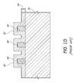
- a layer 50 of spacer materialis subsequently deposited over the mandrels 40 , as shown in FIG. 1D .
- Spacers 60i.e., the material extending or originally formed extending from sidewalls of another material, are then formed on the sides of the mandrels 40 .
- the spacer formationis accomplished by preferentially etching the spacer material from the horizontal surfaces 70 and 80 in a directional spacer etch, as shown in FIG. 1E .
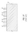
- the remaining mandrels 40are then removed, leaving behind only the spacers 60 , which together act as a mask for patterning, as shown in FIG. 1F .
- the same widthnow includes two features and two spaces, with the spaces defined by, e.g., the spacers 60 .
- the smallest feature size possible with a photolithographic techniqueis effectively decreased.
- pitch doublingthis reduction in pitch is conventionally referred to as pitch “doubling,” or, more generally, pitch “multiplication.”
- pitch “multiplication” of pitch by a certain factoractually involves reducing the pitch by that factor.
- the conventional terminologyis retained herein.
- pitch multiplicationis generally useful for forming regularly spaced linear features, such as conductive lines in a memory array.
- integrated circuitscontain more isolated features, e.g., conductive contacts.
- the continuing reduction in the sizes of integrated circuitshas provided a continuing demand for reductions in the sizes of these isolated features and for increases in the densities of these features.
- Micromasking techniquessuch as isotropically etching mask features, can reduce feature size but do not allow for a corresponding increase in feature density.
- a methodfor semiconductor fabrication.
- the methodcomprises forming a first set of spacers on a first level by pitch multiplication. Spacers of the first set of spacers are elongated substantially in a first direction. A second set of spacers is formed on a second level by pitch multiplication. Spacers of the second set of spacers are elongated substantially in a second direction, which crosses the first direction.
- the methodalso comprises selectively etching one or more layers underlying the first and the second set of spacers through a mask defined by the first and the second set of spacers.
- a methodfor forming an integrated circuit.
- the methodcomprises forming a first plurality of mandrels on a first level above a substrate.
- a first plurality of spacersis formed on sidewalls of the first plurality of mandrels.
- a second plurality of mandrelsis formed on a second level above the first level.
- a second plurality of spacersis formed on sidewalls of the second plurality of mandrels.
- the first and the second plurality of mandrelsare subsequently subjected to an anisotropic etch selective for materials forming the first and the second plurality of mandrels relative to materials forming the first and the second plurality of spacers.
- a methodfor semiconductor processing.
- the methodcomprises forming a set of temporary placeholders.
- a first set of spacersis formed immediately adjacent and contacting the placeholders.
- the first set of spacershave a sub-lithographic pitch.
- a second set of spacersis formed above the first set of spacers.
- the spacers of the second set of spacershave a sub-lithographic pitch and are non-parallel to the first set of spacers.
- At least a portion of the temporary placeholdersare exposed to a directional etch after forming the second set of spacers.
- a mask pattern overlying a partially fabricated integrated circuitcomprises a first plurality of elongated spacers on a first level and a second plurality of elongated spacers on a second level. Spacers of the first plurality of spacers and spacers of the second plurality of spacers extend at an angle of about 30-90° relative to one another.
- FIGS. 1A-1Fare schematic, cross-sectional side views of a sequence of masking patterns for forming conductive lines, in accordance with a prior art pitch doubling method
- FIGS. 2A and 2Bare schematic cross-sectional side and top plan views of a part of a partially formed integrated circuit, in accordance with preferred embodiments of the invention.
- FIGS. 3A and 3Bare schematic cross-sectional side and top plan views of the partially formed integrated circuit of FIGS. 2A and 2B after forming lines in a photoresist layer, in accordance with preferred embodiments of the invention;
- FIGS. 4A and 4Bare schematic cross-sectional side and top plan views of the partially formed integrated circuit of FIGS. 3A and 3B after widening spaces between lines in the photoresist layer, in accordance with preferred embodiments of the invention;
- FIG. 5is a schematic, cross-sectional side view of the partially formed integrated circuit of FIGS. 4A and 4B after etching through a hard mask layer, in accordance with preferred embodiments of the invention
- FIG. 6is a schematic, cross-sectional side view of the partially formed integrated circuit of FIG. 5 after transferring a pattern from the hard mask layer to a temporary or mandrel layer to form mandrels on a first level, in accordance with preferred embodiments of the invention;
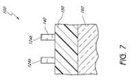
- FIG. 7is a schematic, cross-sectional side view of the partially formed integrated circuit of FIG. 6 after a hard mask layer removal, in accordance with preferred embodiments of the invention.
- FIG. 8is a schematic, cross-sectional side view of the partially formed integrated circuit of FIG. 7 after depositing a layer of a spacer material, in accordance with preferred embodiments of the invention.
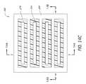
- FIGS. 9A and 9Bare schematic, cross-sectional side and top plan views of the partially formed integrated circuit of FIG. 8 after a spacer etch to define spacers on the first level, in accordance with preferred embodiments of the invention.
- FIGS. 10A and 10Bare schematic, cross-sectional side and top plan views of the partially formed integrated circuit of FIGS. 9A and 9B after forming a planarization, or second mandrel, layer, in accordance with preferred embodiments of the invention;
- FIG. 11is a schematic, cross-sectional side view of the partially formed integrated circuit of FIGS. 10A and 10B after depositing a hard mask layer and a photodefinable layer, respectively, in accordance with preferred embodiments of the invention;
- FIGS. 12A and 12Bare schematic, cross-sectional side views of the partially formed integrated circuit of FIG. 11 after forming a pattern of mandrels in the planarization layer, on a second level, in accordance with preferred embodiments of the invention;
- FIG. 13is a schematic, cross-sectional side view of the partially formed integrated circuit of FIG. 12 after depositing a spacer material around the mandrels, in accordance with preferred embodiments of the invention
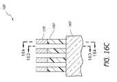
- FIGS. 14A and 14Bare schematic, cross-sectional side views and FIG. 14C is a top plan view of the partially formed integrated circuit of FIG. 13 after performing a spacer etch to form spacers on a second level over the planarization layer, in accordance with preferred embodiments of the invention;
- FIGS. 15A and 15Bare schematic, cross-sectional side views and FIG. 15C is a top plan view of the partially formed integrated circuit of FIGS. 14A-14C after directionally etching exposed mandrel material on the first and the second levels, in accordance with preferred embodiments of the invention;
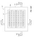
- FIGS. 16A , 16 B, 16 C and 16 Dare schematic, cross-sectional side views and FIG. 16E is a top plan view of the partially formed integrated circuit of FIGS. 15A-15C after transferring a pattern formed by the combination of the spacers on the first and the second levels to an underlying layer, in accordance with preferred embodiments of the invention;
- FIGS. 17A and 17Bare schematic, cross-sectional side and top plan views of the partially formed integrated circuit of FIGS. 16A-16E after removing the spacers on the first and the second levels, in accordance with preferred embodiments of the invention.
- FIG. 18is a top plan view of the partially formed integrated circuit of FIGS. 17A and 17B after filling voids masked by the spacers on the first and the second levels, in accordance with preferred embodiments of the invention.
- pitch-multiplied spacersare formed on multiple levels to define isolated features.
- the spacers on different levelsextend or are elongated substantially in directions or axes that form an angle relative to spacers on other levels, so that the spacers on different levels appear to cross or intersect when viewed in a top down view.
- the angleis about 30°-90°.
- the spacersare formed on two levels and the spacers on a first level are orthogonal to the spacers on a second level.
- the spacers on each levelare preferably formed by pitch multiplication in which mandrels are formed and the spacers are formed on the sides of each of the mandrels.
- a plurality of mandrelsis formed on each level, to form a plurality of spacers on each level. Exposed portions of the mandrels between the spacers are preferably removed after formation of the various sets of spacers, thereby forming voids bounded by the various spacers on the various levels.
- the pattern formed by the spacersis transferred to one or more underlying materials, e.g., an oxide to form an array of vias which can later be filled to form individual circuit elements, e.g., contacts or memory storage devices, in an integrated circuit.
- the spacers or the material underlying the spacersis removed to define a plurality of standalone, up-right, pillar-like structures for forming various electrical devices, e.g., vertical surround transistors formed by etching the substrate.
- spacersare formed on a first level.
- FIGS. 2A and 2Bshow cross-sectional side and top plan views of a portion of an integrated circuit 100 . While the preferred embodiments can be used to form any integrated circuit, they are particularly advantageously applied to forming devices having arrays of electrical devices, including memory cell arrays for volatile and non-volatile memory devices such as DRAM, phase change memory (PCM), programmable conductor RAM (PCRAM), ROM or flash memory, including NAND flash memory, or integrated circuits having logic or gate arrays.
- the logic arraycan be a field programmable gate array (FPGA) having a core array similar to a memory array and a periphery with supporting logics. Consequently, the integrated circuit 100 can be, e.g., a memory chip or a processor, which can include both a logic array and embedded memory, or any other integrated circuit having a logic or a gate array.
- FPGAfield programmable gate array
- various masking layers 120 - 140are preferably provided above a dielectric or insulating layer 150 , which is disposed above a substrate 160 in the illustrated embodiment.
- the layers 120 - 140will be etched to form a mask for patterning the dielectric layer 150 , as discussed below.
- the dielectric layer 150comprises silicon oxide.
- the materials for the layers 120 - 140 overlying the dielectric layer 150are preferably chosen based upon consideration of the chemistry and process conditions for the various pattern forming and pattern transferring steps discussed herein. Because the layers between a topmost selectively definable layer 120 and the dielectric layer 150 preferably function to transfer a pattern derived from the selectively definable layer 120 to the dielectric layer 150 , the layers 130 - 140 between the selectively definable layer 120 and the dielectric layer 150 are preferably chosen so that they can be selectively etched relative to other exposed materials.
- a materialis considered selectively, or preferentially, etched when the etch rate for that material is at least about 2-3 times greater, preferably at least about 10 times greater, more preferably at least about 20 times greater and, most preferably, at least about 40 times greater than that for surrounding materials.
- the layers 120 - 140can be omitted or substituted, or additional layers can be added, if suitable other materials, chemistries and/or process conditions are used.
- the layer 130can be omitted in some embodiments where the resolution enhancement properties of that layer, as discussed below, are not desired.
- the selectively definable layer 120overlies a first hard mask, or etch stop, layer 130 , which overlies a temporary layer 140 , which overlies the dielectric layer 150 to be processed (e.g., etched) through a mask.
- the temporary layer 140can also be referred to as a mandrel layer.
- the mask through which the dielectric layer 150 is processedis formed of spacers 175 and 275 ( FIGS. 15A and 15B ), as discussed below.
- the selectively definable layer 120is preferably photodefinable, e.g., formed of a photoresist, including any photoresist known in the art.
- the photoresistcan be any photoresist compatible with 157 nm, 193 nm, 248 nm or 365 nm wavelength systems, 193 nm wavelength immersion systems, extreme ultraviolet systems (including 13.7 nm wavelength systems) or electron beam lithographic systems.
- maskless lithography, or maskless photolithographycan be used to define the selectively definable layer 120 .
- photoresist materialsinclude argon fluoride (ArF) sensitive photoresist, i.e., photoresist suitable for use with an ArF light source, and krypton fluoride (KrF) sensitive photoresist, i.e., photoresist suitable for use with a KrF light source.
- ArF photoresistsare preferably used with photolithography systems utilizing relatively short wavelength light, e.g., 193 nm.
- KrF photoresistsare preferably used with longer wavelength photolithography systems, such as 248 nm systems.
- the layer 120 and any subsequent resist layerscan be formed of a resist that can be patterned by nano-imprint lithography, e.g., by using a mold or mechanical force to pattern the resist.
- the material for the hard mask layer 130preferably comprises an inorganic material.
- Exemplary materialsinclude silicon oxide (SiO 2 ), silicon or a dielectric anti-reflective coating (DARC), such as a silicon-rich silicon oxynitride.
- the hard mask layer 130is a DARC.
- DARCs for the hard mask layer 130can be particularly advantageous for forming patterns having pitches near the resolution limits of a photolithographic technique. The DARCs can enhance resolution by minimizing light reflections, thus increasing the precision with which photolithography can define the edges of a pattern.
- the temporary layer 140is preferably formed of amorphous carbon. More preferably, the amorphous carbon is a form of amorphous carbon that is highly transparent to light and that offers further improvements for photo alignment by being transparent to the wavelengths of light used for such alignment. Deposition techniques for forming such transparent carbon can be found in A. Helmbold and D. Meissner, Thin Solid Films, 283 (1996) 196-203, the entire disclosure of which is incorporated herein by reference. It will be appreciated that the oxide is preferably a form of silicon oxide and the nitride is preferably a form of silicon nitride.
- the material for the temporary layer 140is preferably chosen based upon the materials used for the lower level spacers 175 ( FIGS. 9A and 9B ), the upper level spacers 275 ( FIGS. 14 and 14B ) and the underlying dielectric layer 150 .
- the layer 140is preferably formed of amorphous carbon. An exemplary combination of materials is listed in the table below:
- the thicknesses of the layers 120 - 140are preferably chosen depending upon compatibility with the etch chemistries and process conditions described herein. As discussed above, when etching a material through a mask of another material, e.g., when transferring a pattern from an overlying layer to an underlying layer by selectively etching the underlying layer, materials from both layers are removed to some degree. Thus, the upper layer is preferably thick enough so that it is not worn away over the course of the pattern transfer.
- the photodefinable layer 120is preferably about 50-300 nm thick and, more preferably, about 200-250 nm thick. It will be appreciated that, in cases where the layer 120 is a photoresist, this thickness can vary depending upon the wavelength of light used to pattern the layer 120 . A thickness of about 50-300 nm thick and, more preferably, about 200-250 nm thick is particularly advantageous for 248 nm wavelength systems.
- the hard mask layer 130is preferably about 10-40 nm thick and, more preferably, about 15-30 nm thick.
- the temporary layer 140is preferably about 50-200 nm thick and, more preferably, about 80-120 nm thick. Because spacers 175 are formed around mandrels 124 b ( FIG. 9A ), which are formed from the temporary layer 140 , and because the spacers 175 are used as a mask in etching underlying material, the height of the spacers 175 is typically determined by the height of the mandrels 140 . As a result, the height of the temporary layer 140 is preferably chosen to form spacers 175 with a height sufficient to account for removal of spacer material during etching of underlying material. It will be appreciated that the height of the spacers can be limited by the structural integrity and the aspect ratio of the spacers, since very tall spacers may collapse or otherwise deform.
- the various layers discussed hereincan be formed by various methods known in the art. For example, spin-on-coating processes can be used to form photodefinable layers. Various deposition processes, such as sputtering, chemical vapor deposition or atomic layer deposition, can be used to form other layers, such as the hard mask layers.
- a low temperature chemical vapor deposition (CVD) processis used to deposit the hard mask layer 130 or any other materials, e.g., a spacer material, over the temporary layer 140 , especially in cases where the temporary layer 140 is formed of amorphous carbon.
- materialsare deposited on the temporary layer 140 , or other layers formed of amorphous carbon, at temperatures of less than about 550° C. and, more preferably, less than about 450° C. and, most preferably, less than about 400° C.
- Such low temperature deposition processesadvantageously prevent chemical or physical disruption of the amorphous carbon layer(s).
- the amorphous carbon layers described hereincan be formed by chemical vapor deposition using a hydrocarbon compound, or mixtures of such compounds, as carbon precursors.
- exemplary precursorsinclude propylene, propyne, propane, butane, butylene, butadiene and acetelyne.
- a suitable method for forming amorphous carbon layersis described in U.S. Pat. No. 6,573,030 B1, issued to Fairbairn et al. on Jun. 3, 2003, the entire disclosure of which is incorporated herein by reference.
- the amorphous carbonmay be doped.
- a suitable method for forming doped amorphous carbonis described in U.S. patent application Ser. No. 10/652,174 to Yin et al., filed Aug. 22, 2003, the entire disclosure of which is incorporated herein by reference.
- the trenches 122can be formed by, e.g., photolithography with 248 nm or 193 nm light, in which the layer 120 is exposed to radiation through a reticle and then developed. After being developed, the remaining photodefinable material, photoresist in the illustrated embodiment, forms mask features such as the illustrated lines 124 (shown in cross-section only).
- the pitch of the resulting lines 124is equal to the sum of the width of a line 124 and the width of a neighboring space 122 .
- the pitchcan be at or near the limits of the photolithographic technique used to pattern the photodefinable layer 120 .
- the pitch of the lines 124can be about 100 nm.
- the pitchmay be at the minimum pitch of the photolithographic technique and the spacer pattern discussed below can advantageously have a pitch below the minimum pitch of the photolithographic technique.
- the lines 124can be formed having larger feature sizes, e.g., 200 nm, to minimize errors in the positions and sizes of the lines 124 .
- the spaces 122are preferably widened by etching the photoresist lines 124 , to form modified spaces 122 a and lines 124 a .
- the photoresist lines 124are preferably etched using an isotropic etch to “shrink” those features. Suitable etches include etches using an oxygen-containing plasma, e.g., a SO 2 /O 2 /N 2 /Ar, Cl 2 /O 2 /He or HBr/O 2 /N 2 plasma.
- the extent of the etchis preferably selected so that the widths of the lines 124 a are substantially equal to the desired spacing between the later-formed spacers 175 , as will be appreciated from the discussion below.
- the width of the lines 124can be reduced from about 80-120 nm to about 35-70 nm and, more preferably, about 40-50 nm.
- the width-reducing etchallows the lines 124 a to be narrower than would otherwise be possible using the photolithographic technique used to pattern the photodefinable layer 120 .
- the etchcan smooth the edges of the lines 124 a , thus improving the uniformity of those lines.
- the pattern in the (modified) photodefinable layer 120 ais transferred to the hard mask layer 130 .
- This transferis preferably accomplished using an anisotropic etch, such as an etch using a fluorocarbon plasma, although a wet (isotropic) etch may also be suitable if the hard mask layer 130 is thin.
- Preferred fluorocarbon plasma etch chemistriesinclude CFH 3 , CF 2 H 2 , CF 3 H and/or CF 4 /HBr for etching the illustrated DARC material.
- the pattern in the photodefinable layer 120 a and the hard mask layer 130is transferred to the temporary layer 140 to allow for deposition of a layer 170 of spacer material ( FIG. 8 ). It has been found that the temperatures used for spacer material deposition are typically too high for photoresist to withstand. Thus, the pattern is preferably transferred from the photodefinable layer 120 a to the temporary layer 140 , which is formed of a material that can withstand the process conditions for spacer material deposition and etch, discussed below. In addition to having higher heat resistance than photoresist, the material forming the temporary layer 140 is preferably selected such that it can be selectively removed relative to the material for the spacers 175 ( FIGS. 9A and 9B ), the spacers 275 ( FIGS. 14A and 14B ) and the underlying dielectric layer 150 . As noted above, the layer 140 is preferably formed of amorphous carbon and, more preferably, transparent carbon.
- the pattern in the modified photodefinable layer 120 ais preferably transferred to the temporary layer 140 using a O 2 -containing plasma, e.g., a plasma containing SO 2 , O 2 and Ar.
- a O 2 -containing plasmae.g., a plasma containing SO 2 , O 2 and Ar.
- etch chemistriesinclude a Cl 2 /O 2 /SiCl 4 or SiCl 4 /O 2 /N 2 or HBr/O 2 /N 2 /SiCl 4 -containing plasma.
- the SO 2 -containing plasmais used as it can etch carbon of the preferred temporary layer 140 at a rate greater than 20 times and, more preferably, greater than 40 times the rate that the hard mask layer 130 is etched.
- the etch chemistryis also preferably selective for the temporary layer 140 relative to the layer 150 or any intervening hard mask or etch stop layers (not shown) present between the layers 140 and 150 .
- a suitable SO 2 -containing plasmais described in U.S. patent application Ser. No. 10/931,772 to Abatchev et al., filed Aug. 31, 2004, the entire disclosure of which is incorporate herein by reference. It will be appreciated that the SO 2 -containing plasma can simultaneously etch the temporary layer 140 and also remove the photodefinable layer 120 a .
- the resulting lines 124 bconstitute the placeholders or mandrels along which a pattern of spacers 175 ( FIGS. 9A and 9B ) will be formed.
- the hard mask layer 130can be removed to facilitate later mask formation by leaving the mandrels 124 b exposed for subsequent etching ( FIGS. 15A and 15B ).
- the preferred hard mask layer 130can be removed using a directional etch, or a wet etch with sufficient selectivity for the material of the layer 130 , as known in the art.
- a layer 170 of spacer materialis preferably blanket deposited conformally over exposed surfaces, including the dielectric layer 150 and the top and sidewalls of the temporary layer 140 .
- the spacer materialis preferably a material that can act as a mask for transferring a pattern to the underlying dielectric layer layer 150 .
- the spacer materialpreferably: 1) can be deposited with good step coverage; 2) can be deposited at a temperature compatible with the temporary layer 140 ; and 3) can be selectively etched relative to the temporary layer 140 and the dielectric layer 150 .
- Preferred materialsinclude silicon, silicon oxides and silicon nitrides.
- the spacer materialis amorphous silicon, which provides particular advantages in combination with other selected materials of the masking stack.
- Preferred methods for spacer material depositioninclude chemical vapor deposition and atomic layer deposition.
- a plasma-enhanced CVDis used to deposit amorphous silicon by using SiH 4 and He in an Applied Materials' ProducerTM system.
- the thickness of the layer 170is preferably determined based upon the desired width of the spacers 175 ( FIGS. 9A-9B ).
- the layer 170is preferably deposited to a thickness of about 20-80 nm and, more preferably, about 50-75 nm.
- the step coverageis about 80% or greater and, more preferably, about 90% or greater.
- the amorphous silicon spacer layer 170is then subjected to an anisotropic etch to remove spacer material from horizontal surfaces 180 of the partially formed integrated circuit 100 .
- an etchalso known as a spacer etch, can be performed using, e.g., a HBr/Cl 2 -containing plasma.
- pitch multiplicationhas been accomplished to form spacers 175 .
- the pitch of the spacers 175is roughly half that of the photoresist lines 124 and spaces 122 ( FIGS. 3A-3B ) originally formed by photolithography.
- spacers 175having a pitch of about 100 nm or less (for a width of about 50 nm) can be formed. It will be appreciated that because the spacers 175 are formed on the sidewalls of the features or lines 124 b , the spacers 175 generally follow the outline of the pattern of features or lines 124 a in the modified photodefinable layer 120 a and, so, typically form a closed loop in the spaces 122 a between the lines 124 a , as illustrated in FIG. 9B .
- additional spacersare formed on a second level.
- the additional spacersare formed extending in a direction that is offset (non-parallel) from the direction in which the spacers 175 extend.
- the mandrels 124 b on the first levelremain in place during the formation of the additional spacers.
- a planar surfaceis formed by depositing a planarizing material which fills the spaces around (between and over) the spacers 175 to form a planarizing layer 200 , as shown in FIGS. 10A-10B .
- the planarizing layer 200is preferably at least as tall as the spacers 175 and, more preferably, is sufficiently tall to allow mandrels to be formed from the planarizing layer 200 and above the spacers 175 , as discussed below.
- the planarizing layer 200is preferably formed of a material selectively etchable relative to both the spacers 175 , the spacers 275 ( FIGS. 14A-14B ) and the dielectric layer 150 .
- the planarization materialis the same material as that used to form the mandrels 124 b .
- the planarization materialcan be amorphous carbon and can be deposited as discussed above with respect to the layer 140 ( FIG. 2A ).
- the planarization material and the mandrel materialcan be different materials or combinations of materials.
- the mandrels 124 bare preferably retained between the spacers 175 , thereby eliminating the need to deposit material into the spaces occupied by the mandrels 124 b . It will be appreciated that those spaces can be narrow and, given that substantially vertical spacer walls delimit the spaces occupied by the mandrels 124 b , the aspect ratio of the spaces can be large and deposition into those spaces can be difficult.
- retention of the mandrels 124 beliminates the need for deposition into those spaces, thereby allowing the formation of a more conformal, uniform planarizing layer 200 .
- the trenches 210 between the spacers 175are of a similar width as the mandrels 124 b in the illustrated embodiment, deposition into the trenches 210 is less difficult than deposition into the space occupied by the mandrels 124 b , since the curved spacer surfaces 220 delimiting those trenches 210 advantageously facilitate deposition of the planarization material into those trenches 210 . It will be appreciated that the curved spacer surfaces can effectively reduce the aspect ratio of the trenches 210 and/or aid in funneling deposition material or precursors into those trenches 210 .
- the planarizing or second mandrel layer 200can optionally be subjected to a planarization process. Such a process can be desirable, e.g., if the planarizing layer 200 is not sufficiently flat to allow for high quality results in subsequent photolithography steps.
- the planarizing layer 200can be subjected to a chemical mechanical polishing (CMP).
- CMPchemical mechanical polishing
- one or more additional layerscan be deposited and then etched and/or subjected to CMP to form a highly planar top surface.
- a bottom anti-reflective coatingcan be deposited and subjected to a dry etch to form a highly planar surface over the planarizing layer 200 .
- the planarization materialcan be a reflowable material such as borophosphosilicate glass or spin-on glass, which can be deposited and then subjected to an anneal to form a highly planar surface.
- the planarization materialis amorphous carbon, which is preferably deposited to a height sufficient to allow the formation of mandrels from the planarizing layer 200 .
- a sequence of layers 250 - 260is deposited to allow patterning of mandrels in the planarizing layer 200 .
- a hard mask layer 250comprising, e.g., a DARC
- a photodefinable layer 260comprising, e.g., a photoresist
- the photoresist layer 260can be etched, trimmed and the resulting pattern can be transferred to the hard mask layer 250 and then transferred to the planarizing layer 200 to form a pattern of mandrels 224 , as shown in FIGS. 12A and 12B .
- a spacer layer 270is deposited around the mandrels 224 .
- the spacer layer 270can be formed of any material having deposition and etch properties compatible with the other materials used herein.
- the spacer materialis silicon oxide which is preferably deposited at a temperature of less than about 550° C. and, more preferably, less than about 450° C. and, most preferably, less than about 400° C.
- the silicon oxidecan be deposited by chemical vapor deposition, e.g., using O 3 and TEOS in a deposition system such as Applied Materials' Producer® HARPTM system. Because a dimension of the contact vias 310 ( FIGS.
- the thickness of the spacer layer 270is preferably chosen with reference to the distance between the mandrels 224 and with reference to the desired size of the contact vias to be formed using the spacers 275 as a mask. In the illustrated embodiment, the thickness of the spacer layer 270 is preferably about 50-75 nm to form contact vias having widths and lengths of about 50 nm.
- a spacer etchis performed to form the spacers 275 , which are preferably orthogonal to the spacers 175 .
- the spacer etchpreferably comprises a fluorocarbon plasma, e.g., a CF 4 /CHF 3 , C 4 F 8 /CH 2 F 2 or CHF 3 /Ar-containing plasma.
- FIG. 14Ais a cross-sectional view, taken along a plane perpendicular to the length of the spacers 175 , of the partially fabricated integrated circuit 100 .
- FIG. 14Bis a cross-sectional view, taken along a plane perpendicular to the length of the spacers 275 , of the partially fabricated integrated circuit 100 .
- FIG. 14Cis a top view of the integrated circuit 100 .
- the mandrels 224 and the planarizing layer 200are preferably selectively anisotropically etched relative to the spacers 175 and 275 .
- suitable etch chemistriesare O 2 -containing plasmas, e.g., a SO 2 /O 2 /Ar, Cl 2 /O 2 /SiCl 4 , SiCl 4 /O 2 /N 2 or HBr/O 2 /N 2 /SiCl 4 -containing plasma.
- the spacers 275shield parts 200 a of the second planarizing or mandrel layer 200 from the etch.
- the unetched parts 200 a of the layer 200support the spacers 275 above the level of the spacers 175 .
- a pattern 300comprising a matrix of orthogonal mask lines comprising the spacers 175 and 275 is formed above the dielectric layer 150 .
- the pattern 300can be transferred to the underlying dielectric layer 150 .
- the dielectric layer 150is selectively etched relative to the spacers 175 and 275 .
- the lower or first spacers 175act as a hard mask in a first lateral direction and the upper or second spacers 275 act as a hard mask in a second lateral direction orthogonal to the first direction.
- An example of a suitable etch for the dielectric layer 150is an anisotropic etch comprising a fluorocarbon plasma, e.g., a CF 4 /CHF 3 , C 4 F 8 /CH 2 F 2 or CHF 3 /Ar-containing plasma.
- the spacers 275 and the dielectric layer 150are formed of the same material, both materials will be etched when transferring the pattern 300 to the dielectric layer.
- the parts 200 a of the planarizing, or second mandrel layer 200 that have the same pattern as the upper spacers 275can function as another layer of hard mask material, thereby allowing the etch of the dielectric layer 150 to be completed.
- the dielectric layer 150can be etched through, thereby forming voids 310 that extend to the substrate 160 .
- the substrate 160is visible in the top view and the lower spacers 175 and temporary layer parts 200 a overlie the unetched dielectric material 150 a ( FIG. 16A ) remaining from the dielectric layer 150 .
- the spacers 175 and parts 200 acan be removed.
- the spacers 175can be removed using an anisotropic etch comprising, e.g., a HBr/Cl 2 -containing plasma
- the parts 200 acan be removed using an anisotropic etch comprising an O 2 -containing plasma, e.g., a SO 2 /O 2 /Ar, Cl 2 /O 2 /SiCl 4 , SiCl 4 /O 2 /N 2 or HBr/O 2 /N 2 /SiCl 4 -containing plasma.
- the voids 310can be filled with various materials, in various applications where voids, particularly arrays of voids, are desired.
- contacts to various conductive featurescan be formed by filling the voids with a conductive material.
- the substratecan comprise conductive interconnect lines, to which the voids 310 open to expose the conductive lines.
- Conductive plugs 320can be formed by filling the voids 310 with a conductive material, e.g., a silicide, tungsten, doped polysilicon, titanium, tantalum, nickel and compounds thereof, including metal nitrides, such titanium nitride and titanium nitride tungsten compounds.
- the voidscan be filled by various deposition processes, including, e.g., CVD.
- a self-directed, selective electrochemical deposition of metal into the voids 310may also be accomplished by using the exposed conductive lines as a seed layer.
- the voids 310can be filled with phase change materials, which change conductivity with switchable changes in phase, in a process to form phase change memories or programmable conductor memories (PCRAM); filled with fusable materials (e.g., positively or negatively doped polysilicon or metals) in a process to form programmable read only memories (PROMs); etc.
- Phase change memoriesare memories having a material which can be switched between relatively conductive and insulating states by the application of heat.
- Examplary phase change materialsinclude germanium, antimony and tellurium alloys (also referred to as GeSbT or GST).
- PCRAMProgrammable conductor RAM
- a programmable conductore.g., chalcogenide glass doped with silver or other high mobility metal
- the conductorscan cause shorts in the glass when an electric field is applied in one direction and can dissolve back into an insulating amorphous glass phase when an opposite electric field is applied.
- Fusable materials in PROMscan be used as fuses, which are retained or “blown” as desired to establish a desired conductive state in the memory.
- electrical devices and/or parts thereof, such as capacitorsmay be formed using the voids 310 .
- arrays of isolated featurese.g., voids, having widths and lengths of about 15-70 nm, more preferably, about 20-60 nm and, most preferably, about 30-55, can be formed using pitch multiplication.
- the sizes of the voidscan be substantially uniform, or the widths and lengths of the voids can be made to alternate between different sizes, e.g., two or three different sizes, by appropriately selecting the thickness of the spacers and the separation between the mandrels. It will be appreciated that the mandrels 140 ( FIG. 9B) and 224 ( FIG. 14B ) and the separation between the spacers 175 ( FIG. 9B) and 275 ( FIG. 14B ), respectively, determine the widths and/or lengths of columns and rows of voids 310 (FIG. 17 B).
- the sizes of the voids 310can be made to alternate in a regular way. For example, by setting the separation between spacers 175 and 275 at one value and the width of the mandrels 130 and 224 at another value, a pattern of large squares (formed by the intersection of the separations between the spacers), relatively small rectangles (formed by the intersection of the separations between the spacers and the space occupied by the mandrels) and relatively smaller squares (formed by the intersection of the mandrels spaces), can be formed.
- the shape of the opening of the voidscan advantageously be varied as desired.
- squarescan be formed by forming uniformly sized and spaced spacers on two levels.
- rectanglescan be formed by spacing spacers farther apart on one level than the other level.
- other parallelogramscan be formed by forming the spacers 175 and 275 at an angle other than about 90° relative to one another (the angle as determined from a top down view of the spacers 175 and 275 ).
- openings of other shapescan be formed by using more than two levels of spacers. For example, by forming two additional levels of spacers, each forming an angle of about 45° relative to existing spacers, octagon-shaped voids can be formed.
- the dielectric layer 150is illustrated as a single layer of a single material for ease of illustration and description, the dielectric layer 150 can comprise multiple stratified materials and/or different materials embedded within one or more levels of material(s). In such cases, if necessary, multiple etches may be utilized to etch through the various layers. In some embodiments, to facilitate the etch of the layer 150 , the pattern formed by the spacers 175 and 275 can be transferred to another hard mask layer which has a high etch selectivity relative to the material(s) of the layer 150 .
- Such a hard mask layercan comprise, e.g., amorphous carbon, which as a high etch selectivity relative to many of the materials discussed herein.
- the layer 150can comprise other materials, which may be insulating and/or conducting, or the mask may be formed directly on the substrate 160 .
- the layer 150can also be etched through the open spaces between the overlapping spacers 175 and 275 or the material exposed by the open spaces can be retained and the material underlying the spacers 175 and 275 can be selectively removed to form a pattern of pillars.
- an inverse mask pattern to that of FIG. 15Bcan be formed by depositing a material into the open spaces and etching back (e.g., by CMP), and the spacers 175 and 275 and the temporary layer material 200 a can be removed to leave a pattern of mask pillars for etching the layer 150 .
- a material underlying the spacers 175 and 275can be selectively converted to another material (e.g., by cross-linking or photo-developing) through the open spaces and the unconverted material can be removed to form a pattern of pillars.
- the pillarscan be the final structures and in other embodiments, these pillars can comprise a hard mask material for etching an underlying material, such as the layer 150 .
- pitch multiplied patternstypically form closed loops, since the patterns are formed by spacers that are formed along the wall of a mandrel, e.g., around the exterior of a free-standing mandrel or in the interior of a cavity, along the walls of mandrels delimiting the cavity.
- the dimensions and placement of the spacers on the various levelsare chosen such that the ends of the closed loops overlap the peripheral spacers (e.g., the first or the last) of an overlying or underlying set of spacers, as shown in FIGS. 15C and 16E .
- a pattern of regularly spaced and dimensioned spacerscan be formed.
- the ends of the spacer loopsmay be formed protruding beyond the peripheral spacers.
- additional processing stepscan be used to cut off the ends of these loops, so that each loop forms two individual, non-connected lines. This can be accomplished, for example, by forming a protective mask around the parts of the lines to be maintained, while etching away the unprotected ends of the masks.
- a suitable method for cutting off the ends of the loopsis disclosed in U.S. patent application Ser. No. 10/931,771 to Tran et al., filed Aug. 31, 2004, the entire disclosure of which is incorporated be reference herein.
- the spacers 175 and 275can be more than pitch doubled.
- the spacers 175can be further pitch multiplied by forming spacers around the spacers 175 , then removing the spacers 175 , then forming spacers around the spacers that were formerly around the spacers 175 , and so on.
- the width of the spacers 175rather than the width of the mandrels 124 b determine one of the dimensions of isolated features that may be formed using the spacer pattern.
- An exemplary method for further pitch multiplicationis discussed in U.S. Pat. No. 5,328,810 to Lowrey et al.
- the preferred embodimentscan be employed multiple times throughout an integrated circuit fabrication process to form pitch multiplied features in a plurality of layers or vertical levels, which may be vertically contiguous or non-contiguous and vertically separated.
- each of the individual levels to be patternedwould constitute a dielectric layer 150 and the various layers 120 - 260 can be formed over the individual level to be patterned.
- processing through the various mask layerspreferably involves etching an underlying layer
- processing through the mask layerscan involve subjecting layers underlying the mask layers to any semiconductor fabrication process.
- processing through the resultant maskcan involve ion implantation, diffusion doping, depositing, or wet etching, etc. through the mask layers and onto underlying layers.
- the mask layerscan be used as a stop or barrier for chemical mechanical polishing (CMP) or CMP can be performed on any of the layers to allow for both planarization and etching of the underlying layers, as discussed in U.S. Provisional Patent Application No. 60/666,031, filed Mar. 28, 2005, the entire disclosure of which is incorporated by reference herein.
Landscapes
- Engineering & Computer Science (AREA)
- Manufacturing & Machinery (AREA)
- Physics & Mathematics (AREA)
- Condensed Matter Physics & Semiconductors (AREA)
- General Physics & Mathematics (AREA)
- Computer Hardware Design (AREA)
- Microelectronics & Electronic Packaging (AREA)
- Power Engineering (AREA)
- Chemical & Material Sciences (AREA)
- Inorganic Chemistry (AREA)
- Semiconductor Memories (AREA)
- Internal Circuitry In Semiconductor Integrated Circuit Devices (AREA)
Abstract
Description
| Exemplary Spacer, Mandrel Layer, Hard Mask |
| and Underlying Materials |
| Underlying | ||||
| Lower Level | Upper Level | Dielectric | ||
| Spacers | Spacers | Hard Mask | Mandrel Layer | Layer |
| Amorphous | Silicon | DARC | Amorphous | Silicon |
| Silicon | Oxide | Carbon | Oxide | |
Claims (25)
Priority Applications (2)
| Application Number | Priority Date | Filing Date | Title |
|---|---|---|---|
| US12/813,157US8043915B2 (en) | 2005-09-01 | 2010-06-10 | Pitch multiplied mask patterns for isolated features |
| US13/235,722US8431971B2 (en) | 2005-09-01 | 2011-09-19 | Pitch multiplied mask patterns for isolated features |
Applications Claiming Priority (2)
| Application Number | Priority Date | Filing Date | Title |
|---|---|---|---|
| US11/219,067US7759197B2 (en) | 2005-09-01 | 2005-09-01 | Method of forming isolated features using pitch multiplication |
| US12/813,157US8043915B2 (en) | 2005-09-01 | 2010-06-10 | Pitch multiplied mask patterns for isolated features |
Related Parent Applications (1)
| Application Number | Title | Priority Date | Filing Date |
|---|---|---|---|
| US11/219,067DivisionUS7759197B2 (en) | 2005-09-01 | 2005-09-01 | Method of forming isolated features using pitch multiplication |
Related Child Applications (1)
| Application Number | Title | Priority Date | Filing Date |
|---|---|---|---|
| US13/235,722ContinuationUS8431971B2 (en) | 2005-09-01 | 2011-09-19 | Pitch multiplied mask patterns for isolated features |
Publications (2)
| Publication Number | Publication Date |
|---|---|
| US20100243161A1 US20100243161A1 (en) | 2010-09-30 |
| US8043915B2true US8043915B2 (en) | 2011-10-25 |
Family
ID=37804830
Family Applications (3)
| Application Number | Title | Priority Date | Filing Date |
|---|---|---|---|
| US11/219,067Active2027-11-20US7759197B2 (en) | 2005-09-01 | 2005-09-01 | Method of forming isolated features using pitch multiplication |
| US12/813,157Expired - LifetimeUS8043915B2 (en) | 2005-09-01 | 2010-06-10 | Pitch multiplied mask patterns for isolated features |
| US13/235,722Expired - LifetimeUS8431971B2 (en) | 2005-09-01 | 2011-09-19 | Pitch multiplied mask patterns for isolated features |
Family Applications Before (1)
| Application Number | Title | Priority Date | Filing Date |
|---|---|---|---|
| US11/219,067Active2027-11-20US7759197B2 (en) | 2005-09-01 | 2005-09-01 | Method of forming isolated features using pitch multiplication |
Family Applications After (1)
| Application Number | Title | Priority Date | Filing Date |
|---|---|---|---|
| US13/235,722Expired - LifetimeUS8431971B2 (en) | 2005-09-01 | 2011-09-19 | Pitch multiplied mask patterns for isolated features |
Country Status (1)
| Country | Link |
|---|---|
| US (3) | US7759197B2 (en) |
Cited By (8)
| Publication number | Priority date | Publication date | Assignee | Title |
|---|---|---|---|---|
| US20120045901A1 (en)* | 2010-08-19 | 2012-02-23 | Jong-Hyuk Kim | Method of forming a pattern structure for a semiconductor device |
| US20120241975A1 (en)* | 2011-03-24 | 2012-09-27 | Vincent Farys | Method for decomposing lines of an electronic circuit |
| US8889561B2 (en)* | 2012-12-10 | 2014-11-18 | Globalfoundries Inc. | Double sidewall image transfer process |
| US9048292B2 (en) | 2012-10-25 | 2015-06-02 | Micron Technology, Inc. | Patterning methods and methods of forming electrically conductive lines |
| US20150170905A1 (en)* | 2007-07-30 | 2015-06-18 | Micron Technology, Inc. | Methods for device fabrication using pitch reduction and related devices |
| US9437444B2 (en) | 2013-04-30 | 2016-09-06 | SK Hynix Inc. | Semiconductor device having hard mask structure and fine pattern and forming method thereof |
| US20190019676A1 (en)* | 2017-07-15 | 2019-01-17 | Micromaterials Llc | Mask Scheme For Cut Pattern Flow With Enlarged EPE Window |
| US10515801B2 (en) | 2007-06-04 | 2019-12-24 | Micron Technology, Inc. | Pitch multiplication using self-assembling materials |
Families Citing this family (103)
| Publication number | Priority date | Publication date | Assignee | Title |
|---|---|---|---|---|
| US7151040B2 (en)* | 2004-08-31 | 2006-12-19 | Micron Technology, Inc. | Methods for increasing photo alignment margins |
| US7910288B2 (en)* | 2004-09-01 | 2011-03-22 | Micron Technology, Inc. | Mask material conversion |
| US7115525B2 (en)* | 2004-09-02 | 2006-10-03 | Micron Technology, Inc. | Method for integrated circuit fabrication using pitch multiplication |
| US7655387B2 (en)* | 2004-09-02 | 2010-02-02 | Micron Technology, Inc. | Method to align mask patterns |
| US7390746B2 (en) | 2005-03-15 | 2008-06-24 | Micron Technology, Inc. | Multiple deposition for integration of spacers in pitch multiplication process |
| US7253118B2 (en)* | 2005-03-15 | 2007-08-07 | Micron Technology, Inc. | Pitch reduced patterns relative to photolithography features |
| US7611944B2 (en) | 2005-03-28 | 2009-11-03 | Micron Technology, Inc. | Integrated circuit fabrication |
| US7429536B2 (en) | 2005-05-23 | 2008-09-30 | Micron Technology, Inc. | Methods for forming arrays of small, closely spaced features |
| US7560390B2 (en)* | 2005-06-02 | 2009-07-14 | Micron Technology, Inc. | Multiple spacer steps for pitch multiplication |
| US7396781B2 (en)* | 2005-06-09 | 2008-07-08 | Micron Technology, Inc. | Method and apparatus for adjusting feature size and position |
| US7888721B2 (en) | 2005-07-06 | 2011-02-15 | Micron Technology, Inc. | Surround gate access transistors with grown ultra-thin bodies |
| US7768051B2 (en) | 2005-07-25 | 2010-08-03 | Micron Technology, Inc. | DRAM including a vertical surround gate transistor |
| US7413981B2 (en) | 2005-07-29 | 2008-08-19 | Micron Technology, Inc. | Pitch doubled circuit layout |
| US8123968B2 (en)* | 2005-08-25 | 2012-02-28 | Round Rock Research, Llc | Multiple deposition for integration of spacers in pitch multiplication process |
| US7816262B2 (en) | 2005-08-30 | 2010-10-19 | Micron Technology, Inc. | Method and algorithm for random half pitched interconnect layout with constant spacing |
| US7696567B2 (en) | 2005-08-31 | 2010-04-13 | Micron Technology, Inc | Semiconductor memory device |
| US7829262B2 (en)* | 2005-08-31 | 2010-11-09 | Micron Technology, Inc. | Method of forming pitch multipled contacts |
| US7393789B2 (en)* | 2005-09-01 | 2008-07-01 | Micron Technology, Inc. | Protective coating for planarization |
| US7776744B2 (en)* | 2005-09-01 | 2010-08-17 | Micron Technology, Inc. | Pitch multiplication spacers and methods of forming the same |
| US7416943B2 (en)* | 2005-09-01 | 2008-08-26 | Micron Technology, Inc. | Peripheral gate stacks and recessed array gates |
| US7572572B2 (en) | 2005-09-01 | 2009-08-11 | Micron Technology, Inc. | Methods for forming arrays of small, closely spaced features |
| US7759197B2 (en) | 2005-09-01 | 2010-07-20 | Micron Technology, Inc. | Method of forming isolated features using pitch multiplication |
| US7557032B2 (en)* | 2005-09-01 | 2009-07-07 | Micron Technology, Inc. | Silicided recessed silicon |
| US7687342B2 (en)* | 2005-09-01 | 2010-03-30 | Micron Technology, Inc. | Method of manufacturing a memory device |
| WO2007044514A2 (en)* | 2005-10-07 | 2007-04-19 | Lee, Michael, J. | Method for improving refractive index control in pecvd deposited a-siny films |
| US7842558B2 (en)* | 2006-03-02 | 2010-11-30 | Micron Technology, Inc. | Masking process for simultaneously patterning separate regions |
| US7476933B2 (en) | 2006-03-02 | 2009-01-13 | Micron Technology, Inc. | Vertical gated access transistor |
| US7902074B2 (en) | 2006-04-07 | 2011-03-08 | Micron Technology, Inc. | Simplified pitch doubling process flow |
| US8003310B2 (en)* | 2006-04-24 | 2011-08-23 | Micron Technology, Inc. | Masking techniques and templates for dense semiconductor fabrication |
| US7488685B2 (en) | 2006-04-25 | 2009-02-10 | Micron Technology, Inc. | Process for improving critical dimension uniformity of integrated circuit arrays |
| US7795149B2 (en) | 2006-06-01 | 2010-09-14 | Micron Technology, Inc. | Masking techniques and contact imprint reticles for dense semiconductor fabrication |
| US7723009B2 (en) | 2006-06-02 | 2010-05-25 | Micron Technology, Inc. | Topography based patterning |
| US8852851B2 (en) | 2006-07-10 | 2014-10-07 | Micron Technology, Inc. | Pitch reduction technology using alternating spacer depositions during the formation of a semiconductor device and systems including same |
| US7611980B2 (en) | 2006-08-30 | 2009-11-03 | Micron Technology, Inc. | Single spacer process for multiplying pitch by a factor greater than two and related intermediate IC structures |
| US7666578B2 (en)* | 2006-09-14 | 2010-02-23 | Micron Technology, Inc. | Efficient pitch multiplication process |
| US8129289B2 (en) | 2006-10-05 | 2012-03-06 | Micron Technology, Inc. | Method to deposit conformal low temperature SiO2 |
| US20080085600A1 (en)* | 2006-10-10 | 2008-04-10 | Toshiharu Furukawa | Method of forming lithographic and sub-lithographic dimensioned structures |
| US7771896B2 (en)* | 2006-12-22 | 2010-08-10 | Asml Netherlands B.V. | Patterning device, method of providing a patterning device, photolithographic apparatus and device manufacturing method |
| KR100822592B1 (en)* | 2007-03-23 | 2008-04-16 | 주식회사 하이닉스반도체 | Method of forming fine pattern of semiconductor device |
| KR100822621B1 (en)* | 2007-04-06 | 2008-04-16 | 주식회사 하이닉스반도체 | Method of forming fine pattern of semiconductor device |
| US7553770B2 (en)* | 2007-06-06 | 2009-06-30 | Micron Technology, Inc. | Reverse masking profile improvements in high aspect ratio etch |
| US8563229B2 (en)* | 2007-07-31 | 2013-10-22 | Micron Technology, Inc. | Process of semiconductor fabrication with mask overlay on pitch multiplied features and associated structures |
| US8481417B2 (en) | 2007-08-03 | 2013-07-09 | Micron Technology, Inc. | Semiconductor structures including tight pitch contacts and methods to form same |
| US7737039B2 (en) | 2007-11-01 | 2010-06-15 | Micron Technology, Inc. | Spacer process for on pitch contacts and related structures |
| US7659208B2 (en) | 2007-12-06 | 2010-02-09 | Micron Technology, Inc | Method for forming high density patterns |
| US7846812B2 (en)* | 2007-12-18 | 2010-12-07 | Micron Technology, Inc. | Methods of forming trench isolation and methods of forming floating gate transistors |
| US7790531B2 (en) | 2007-12-18 | 2010-09-07 | Micron Technology, Inc. | Methods for isolating portions of a loop of pitch-multiplied material and related structures |
| KR100942078B1 (en)* | 2007-12-27 | 2010-02-12 | 주식회사 하이닉스반도체 | Method of forming fine pattern of semiconductor device |
| US8030218B2 (en) | 2008-03-21 | 2011-10-04 | Micron Technology, Inc. | Method for selectively modifying spacing between pitch multiplied structures |
| US7989307B2 (en) | 2008-05-05 | 2011-08-02 | Micron Technology, Inc. | Methods of forming isolated active areas, trenches, and conductive lines in semiconductor structures and semiconductor structures including the same |
| US10151981B2 (en) | 2008-05-22 | 2018-12-11 | Micron Technology, Inc. | Methods of forming structures supported by semiconductor substrates |
| US20090302472A1 (en)* | 2008-06-05 | 2009-12-10 | Samsung Electronics Co., Ltd. | Non-volatile memory devices including shared bit lines and methods of fabricating the same |
| JP2009295785A (en)* | 2008-06-05 | 2009-12-17 | Toshiba Corp | Method of manufacturing semiconductor device |
| US8076208B2 (en) | 2008-07-03 | 2011-12-13 | Micron Technology, Inc. | Method for forming transistor with high breakdown voltage using pitch multiplication technique |
| US8101497B2 (en)* | 2008-09-11 | 2012-01-24 | Micron Technology, Inc. | Self-aligned trench formation |
| US8492282B2 (en)* | 2008-11-24 | 2013-07-23 | Micron Technology, Inc. | Methods of forming a masking pattern for integrated circuits |
| US8273634B2 (en)* | 2008-12-04 | 2012-09-25 | Micron Technology, Inc. | Methods of fabricating substrates |
| US8247302B2 (en) | 2008-12-04 | 2012-08-21 | Micron Technology, Inc. | Methods of fabricating substrates |
| US8796155B2 (en) | 2008-12-04 | 2014-08-05 | Micron Technology, Inc. | Methods of fabricating substrates |
| US8268543B2 (en)* | 2009-03-23 | 2012-09-18 | Micron Technology, Inc. | Methods of forming patterns on substrates |
| US9330934B2 (en)* | 2009-05-18 | 2016-05-03 | Micron Technology, Inc. | Methods of forming patterns on substrates |
| US8268730B2 (en)* | 2009-06-03 | 2012-09-18 | Micron Technology, Inc. | Methods of masking semiconductor device structures |
| US20110076784A1 (en)* | 2009-09-29 | 2011-03-31 | Grandis Inc. | Fabrication of Magnetic Element Arrays |
| KR20120089697A (en)* | 2009-10-26 | 2012-08-13 | 쌘디스크 3디 엘엘씨 | Apparatus and methods of forming memory lines and structures using double sidewall patterning for four times half pitch relief patterning |
| US8455364B2 (en)* | 2009-11-06 | 2013-06-04 | International Business Machines Corporation | Sidewall image transfer using the lithographic stack as the mandrel |
| US8003482B2 (en) | 2009-11-19 | 2011-08-23 | Micron Technology, Inc. | Methods of processing semiconductor substrates in forming scribe line alignment marks |
| US20110129991A1 (en)* | 2009-12-02 | 2011-06-02 | Kyle Armstrong | Methods Of Patterning Materials, And Methods Of Forming Memory Cells |
| KR101105508B1 (en)* | 2009-12-30 | 2012-01-13 | 주식회사 하이닉스반도체 | Manufacturing Method of Semiconductor Memory Device |
| JP5497476B2 (en)* | 2010-02-25 | 2014-05-21 | 富士フイルム株式会社 | Method for manufacturing solid-state imaging device |
| US8198160B2 (en) | 2010-04-19 | 2012-06-12 | Jun Liu | Vertical transistor phase change memory |
| US8518788B2 (en) | 2010-08-11 | 2013-08-27 | Micron Technology, Inc. | Methods of forming a plurality of capacitors |
| US8455341B2 (en) | 2010-09-02 | 2013-06-04 | Micron Technology, Inc. | Methods of forming features of integrated circuitry |
| US8575032B2 (en) | 2011-05-05 | 2013-11-05 | Micron Technology, Inc. | Methods of forming a pattern on a substrate |
| KR20120126228A (en)* | 2011-05-11 | 2012-11-21 | 삼성전자주식회사 | Methods of forming a pattern and methods of manufacturing a semiconductor device using the same |
| US9076680B2 (en) | 2011-10-18 | 2015-07-07 | Micron Technology, Inc. | Integrated circuitry, methods of forming capacitors, and methods of forming integrated circuitry comprising an array of capacitors and circuitry peripheral to the array |
| KR101903477B1 (en) | 2012-01-11 | 2018-10-02 | 삼성전자주식회사 | Method of fabricating a semiconductor device |
| US9177794B2 (en) | 2012-01-13 | 2015-11-03 | Micron Technology, Inc. | Methods of patterning substrates |
| US8741776B2 (en)* | 2012-02-07 | 2014-06-03 | Taiwan Semiconductor Manufacturing Company, Ltd. | Patterning process for fin-like field effect transistor (finFET) device |
| KR101948222B1 (en) | 2012-06-15 | 2019-02-14 | 에스케이하이닉스 주식회사 | Mask pattern for hole patterning and method for fabricating semiconductor device using the same |
| US8629048B1 (en) | 2012-07-06 | 2014-01-14 | Micron Technology, Inc. | Methods of forming a pattern on a substrate |
| US8647981B1 (en)* | 2012-08-31 | 2014-02-11 | Micron Technology, Inc. | Methods of forming patterns, and methods of forming integrated circuitry |
| US9111857B2 (en)* | 2012-09-21 | 2015-08-18 | Micron Technology, Inc. | Method, system and device for recessed contact in memory array |
| US8853085B1 (en) | 2013-04-23 | 2014-10-07 | International Business Machines Corporation | Grapho-epitaxy DSA process with dimension control of template pattern |
| EP2843696A1 (en)* | 2013-08-27 | 2015-03-04 | IMEC vzw | A method for dopant implantation of FinFET structures |
| US9159579B2 (en)* | 2013-10-25 | 2015-10-13 | Taiwan Semiconductor Manufacturing Company, Ltd. | Lithography using multilayer spacer for reduced spacer footing |
| US9177797B2 (en)* | 2013-12-04 | 2015-11-03 | Taiwan Semiconductor Manufacturing Company, Ltd. | Lithography using high selectivity spacers for pitch reduction |
| TWI545622B (en) | 2014-02-23 | 2016-08-11 | 東京威力科創股份有限公司 | Method for multiplying pattern density by crossing multiple patterned layers |
| US9773888B2 (en) | 2014-02-26 | 2017-09-26 | Micron Technology, Inc. | Vertical access devices, semiconductor device structures, and related methods |
| KR102248436B1 (en) | 2014-05-23 | 2021-05-07 | 삼성전자주식회사 | Methods for fabricating semiconductor devices |
| TWI595556B (en) | 2014-12-19 | 2017-08-11 | 東京威力科創股份有限公司 | Method of forming a mask for substrate patterning |
| KR102310834B1 (en)* | 2014-12-22 | 2021-10-07 | 도쿄엘렉트론가부시키가이샤 | Patterning of Substrates with the Use of Grafting Polymer Materials |
| KR102337410B1 (en) | 2015-04-06 | 2021-12-10 | 삼성전자주식회사 | Method for forming fine patterns of semiconductor device |
| SG11201806451VA (en)* | 2016-01-29 | 2018-08-30 | Tokyo Electron Ltd | Method and system for forming memory fin patterns |
| US10056265B2 (en)* | 2016-03-18 | 2018-08-21 | Taiwan Semiconductor Manufacturing Co., Ltd. | Directed self-assembly process with size-restricted guiding patterns |
| US9882028B2 (en)* | 2016-06-29 | 2018-01-30 | International Business Machines Corporation | Pitch split patterning for semiconductor devices |
| US9947548B2 (en)* | 2016-08-09 | 2018-04-17 | International Business Machines Corporation | Self-aligned single dummy fin cut with tight pitch |
| WO2018063330A1 (en)* | 2016-09-30 | 2018-04-05 | Intel Corporation | Plug & trench architectures for integrated circuits & methods of manufacture |
| CN109309091A (en)* | 2017-07-28 | 2019-02-05 | 联华电子股份有限公司 | patterning method |
| US11417525B2 (en)* | 2018-10-08 | 2022-08-16 | Globalfoundries U.S. Inc. | Multiple patterning with mandrel cuts defined by block masks |
| EP3723112B1 (en)* | 2019-04-09 | 2023-12-20 | Imec Vzw | Method for forming a gate mask layer |
| US11011581B2 (en)* | 2019-06-10 | 2021-05-18 | Western Digital Technologies, Inc. | Multi-level loop cut process for a three-dimensional memory device using pitch-doubled metal lines |
| CN113745151B (en)* | 2020-05-29 | 2024-05-31 | 中芯国际集成电路制造(上海)有限公司 | Semiconductor structure and forming method thereof |
| KR20250010826A (en)* | 2023-07-13 | 2025-01-21 | 삼성전자주식회사 | Semiconductor device and method for fabricating the same |
Citations (170)
| Publication number | Priority date | Publication date | Assignee | Title |
|---|---|---|---|---|
| US4234362A (en) | 1978-11-03 | 1980-11-18 | International Business Machines Corporation | Method for forming an insulator between layers of conductive material |
| US4419809A (en) | 1981-12-30 | 1983-12-13 | International Business Machines Corporation | Fabrication process of sub-micrometer channel length MOSFETs |
| US4432132A (en) | 1981-12-07 | 1984-02-21 | Bell Telephone Laboratories, Incorporated | Formation of sidewall oxide layers by reactive oxygen ion etching to define submicron features |
| US4502914A (en) | 1982-11-13 | 1985-03-05 | International Business Machines Corporation | Method of making structures with dimensions in the sub-micrometer range |
| US4508579A (en) | 1981-03-30 | 1985-04-02 | International Business Machines Corporation | Lateral device structures using self-aligned fabrication techniques |
| US4570325A (en) | 1983-12-16 | 1986-02-18 | Kabushiki Kaisha Toshiba | Manufacturing a field oxide region for a semiconductor device |
| US4648937A (en) | 1985-10-30 | 1987-03-10 | International Business Machines Corporation | Method of preventing asymmetric etching of lines in sub-micrometer range sidewall images transfer |
| EP0227303A2 (en) | 1985-11-25 | 1987-07-01 | Plessey Overseas Limited | Method of manufacturing semiconductor devices having side-wall isolation |
| US4716131A (en) | 1983-11-28 | 1987-12-29 | Nec Corporation | Method of manufacturing semiconductor device having polycrystalline silicon layer with metal silicide film |
| US4776922A (en) | 1987-10-30 | 1988-10-11 | International Business Machines Corporation | Formation of variable-width sidewall structures |
| US4838991A (en) | 1987-10-30 | 1989-06-13 | International Business Machines Corporation | Process for defining organic sidewall structures |
| US5013680A (en) | 1990-07-18 | 1991-05-07 | Micron Technology, Inc. | Process for fabricating a DRAM array having feature widths that transcend the resolution limit of available photolithography |
| US5047117A (en) | 1990-09-26 | 1991-09-10 | Micron Technology, Inc. | Method of forming a narrow self-aligned, annular opening in a masking layer |
| US5053105A (en) | 1990-07-19 | 1991-10-01 | Micron Technology, Inc. | Process for creating an etch mask suitable for deep plasma etches employing self-aligned silicidation of a metal layer masked with a silicon dioxide template |
| US5117027A (en) | 1990-10-31 | 1992-05-26 | Huls Aktiengesellschaft | Process for the preparation of organosilanes containing methacryloyloxy or acryloyloxy groups |
| EP0491408A2 (en) | 1990-11-20 | 1992-06-24 | Consorzio per la Ricerca sulla Microelettronica nel Mezzogiorno - CoRiMMe | Process for making planarized sub-micrometric trenches in integrated circuits |
| DE4236609A1 (en) | 1992-10-29 | 1994-05-05 | Siemens Ag | Method for forming a structure in the surface of a substrate - with an auxiliary structure laterally bounding an initial masking structure, followed by selective removal of masking structure using the auxiliary structure as an etching mask |
| US5328810A (en) | 1990-05-07 | 1994-07-12 | Micron Technology, Inc. | Method for reducing, by a factor or 2-N, the minimum masking pitch of a photolithographic process |
| US5330879A (en) | 1992-07-16 | 1994-07-19 | Micron Technology, Inc. | Method for fabrication of close-tolerance lines and sharp emission tips on a semiconductor wafer |
| US5470661A (en) | 1993-01-07 | 1995-11-28 | International Business Machines Corporation | Diamond-like carbon films from a hydrocarbon helium plasma |
| JPH0855908A (en) | 1994-08-17 | 1996-02-27 | Toshiba Corp | Semiconductor device |
| JPH0855920A (en) | 1994-08-15 | 1996-02-27 | Toshiba Corp | Method for manufacturing semiconductor device |
| US5514885A (en) | 1986-10-09 | 1996-05-07 | Myrick; James J. | SOI methods and apparatus |
| US5593813A (en) | 1994-07-14 | 1997-01-14 | Hyundai Electronics Industries Co. Ltd. | Method for forming submicroscopic patterns |
| US5670794A (en) | 1994-10-07 | 1997-09-23 | Micron Technology, Inc. | Thin film transistors |
| US5753546A (en) | 1995-06-30 | 1998-05-19 | Hyundai Electronics Industries Co., Ltd. | Method for fabricating metal oxide field effect transistors |
| US5789320A (en) | 1996-04-23 | 1998-08-04 | International Business Machines Corporation | Plating of noble metal electrodes for DRAM and FRAM |
| US5795830A (en) | 1995-06-06 | 1998-08-18 | International Business Machines Corporation | Reducing pitch with continuously adjustable line and space dimensions |
| US5830332A (en) | 1995-01-26 | 1998-11-03 | International Business Machines Corporation | Sputter deposition of hydrogenated amorphous carbon film and applications thereof |
| US5899746A (en) | 1995-09-08 | 1999-05-04 | Sony Corporation | Method of forming pattern |
| US5998256A (en) | 1996-11-01 | 1999-12-07 | Micron Technology, Inc. | Semiconductor processing methods of forming devices on a substrate, forming device arrays on a substrate, forming conductive lines on a substrate, and forming capacitor arrays on a substrate, and integrated circuitry |
| TW376582B (en) | 1998-06-26 | 1999-12-11 | Vanguard Int Semiconduct Corp | Method of forming COB DRAM with self-aligned pole and bitline contact plug |
| US6004862A (en) | 1998-01-20 | 1999-12-21 | Advanced Micro Devices, Inc. | Core array and periphery isolation technique |
| US6010946A (en) | 1996-08-21 | 2000-01-04 | Nec Corporation | Semiconductor device with isolation insulating film tapered and method of manufacturing the same |
| US6042998A (en) | 1993-09-30 | 2000-03-28 | The University Of New Mexico | Method and apparatus for extending spatial frequencies in photolithography images |
| US6057573A (en) | 1998-05-27 | 2000-05-02 | Vanguard International Semiconductor Corporation | Design for high density memory with relaxed metal pitch |
| US6060383A (en) | 1998-08-10 | 2000-05-09 | Nogami; Takeshi | Method for making multilayered coaxial interconnect structure |
| US6063688A (en) | 1997-09-29 | 2000-05-16 | Intel Corporation | Fabrication of deep submicron structures and quantum wire transistors using hard-mask transistor width definition |
| US6071789A (en) | 1998-11-10 | 2000-06-06 | Vanguard International Semiconductor Corporation | Method for simultaneously fabricating a DRAM capacitor and metal interconnections |
| US6110837A (en) | 1999-04-28 | 2000-08-29 | Worldwide Semiconductor Manufacturing Corp. | Method for forming a hard mask of half critical dimension |
| US6143476A (en) | 1997-12-12 | 2000-11-07 | Applied Materials Inc | Method for high temperature etching of patterned layers using an organic mask stack |
| US6207490B1 (en) | 1997-12-11 | 2001-03-27 | Samsung Electronics Co., Ltd. | Semiconductor device and method for fabricating the same |
| US6211044B1 (en) | 1999-04-12 | 2001-04-03 | Advanced Micro Devices | Process for fabricating a semiconductor device component using a selective silicidation reaction |
| US20010005631A1 (en) | 1999-12-14 | 2001-06-28 | Jin-Won Kim | Method for manufacturing an electrode of a capacitor |
| US6288454B1 (en) | 1999-05-13 | 2001-09-11 | Lsi Logic Corporation | Semiconductor wafer having a layer-to-layer alignment mark and method for fabricating the same |
| US6291334B1 (en) | 1997-12-19 | 2001-09-18 | Applied Materials, Inc. | Etch stop layer for dual damascene process |
| US6297554B1 (en) | 2000-03-10 | 2001-10-02 | United Microelectronics Corp. | Dual damascene interconnect structure with reduced parasitic capacitance |
| US6335257B1 (en) | 2000-09-29 | 2002-01-01 | Vanguard International Semiconductor Corporation | Method of making pillar-type structure on semiconductor substrate |
| US6348380B1 (en) | 2000-08-25 | 2002-02-19 | Micron Technology, Inc. | Use of dilute steam ambient for improvement of flash devices |
| US6362057B1 (en) | 1999-10-26 | 2002-03-26 | Motorola, Inc. | Method for forming a semiconductor device |
| US20020042198A1 (en) | 2000-09-20 | 2002-04-11 | Bjarni Bjarnason | Method in etching of a substrate |
| US6372649B1 (en) | 1999-06-24 | 2002-04-16 | Hyundai Electronics Industries Co., Ltd. | Method for forming multi-level metal interconnection |
| US20020045308A1 (en) | 1996-11-01 | 2002-04-18 | Werner Juengling | Semiconductor processing methods of forming a plurality of capacitors on a substrate, bit line contacts and method of forming bit line contacts |
| US6383907B1 (en) | 1999-09-08 | 2002-05-07 | Sony Corporation | Process for fabricating a semiconductor device |
| US20020063110A1 (en) | 2000-11-30 | 2002-05-30 | Cantell Marc W. | Etching of hard masks |
| US20020068243A1 (en) | 2000-12-04 | 2002-06-06 | Jiunn-Ren Hwang | Method of forming opening in wafer layer |
| US20020094688A1 (en) | 2001-01-16 | 2002-07-18 | Semiconductor Leading Edge Technologies, Inc. | Method of forming fine patterns |
| US6423474B1 (en) | 2000-03-21 | 2002-07-23 | Micron Technology, Inc. | Use of DARC and BARC in flash memory processing |
| US20020127810A1 (en) | 2000-05-29 | 2002-09-12 | Fujitsu Limited | Semiconductor device and method for fabricating the same |
| US6455372B1 (en) | 2000-08-14 | 2002-09-24 | Micron Technology, Inc. | Nucleation for improved flash erase characteristics |
| US6475867B1 (en) | 2001-04-02 | 2002-11-05 | Advanced Micro Devices, Inc. | Method of forming integrated circuit features by oxidation of titanium hard mask |
| WO2002099864A1 (en) | 2001-05-31 | 2002-12-12 | Infineon Technologies, Ag | Method for removing polysilane from a semiconductor without stripping |
| US6500756B1 (en) | 2002-06-28 | 2002-12-31 | Advanced Micro Devices, Inc. | Method of forming sub-lithographic spaces between polysilicon lines |
| US20030006410A1 (en) | 2000-03-01 | 2003-01-09 | Brian Doyle | Quantum wire gate device and method of making same |
| US6514884B2 (en) | 1998-02-06 | 2003-02-04 | Semiconductor Process Laboratory Co., Ltd. | Method for reforming base surface, method for manufacturing semiconductor device and equipment for manufacturing the same |
| US6522584B1 (en) | 2001-08-02 | 2003-02-18 | Micron Technology, Inc. | Programming methods for multi-level flash EEPROMs |
| US20030044722A1 (en) | 2001-08-28 | 2003-03-06 | Yi-Yu Hsu | Process for improving critical dimension uniformity |
| US6531067B1 (en) | 1998-12-28 | 2003-03-11 | Asahi Kasei Microsystems Co., Ltd. | Method for forming contact hole |
| US6534243B1 (en) | 2000-10-23 | 2003-03-18 | Advanced Micro Devices, Inc. | Chemical feature doubling process |
| US6548396B2 (en) | 1998-07-23 | 2003-04-15 | Applied Materials, Inc. | Method of producing an interconnect structure for an integrated circuit |
| US6559017B1 (en) | 2002-06-13 | 2003-05-06 | Advanced Micro Devices, Inc. | Method of using amorphous carbon as spacer material in a disposable spacer process |
| US20030090002A1 (en) | 2001-09-20 | 2003-05-15 | Akira Sugawara | Semiconductor device and method of manufacturing the same |
| US6566280B1 (en) | 2002-08-26 | 2003-05-20 | Intel Corporation | Forming polymer features on a substrate |
| US6573030B1 (en) | 2000-02-17 | 2003-06-03 | Applied Materials, Inc. | Method for depositing an amorphous carbon layer |
| US20030109102A1 (en) | 2001-10-24 | 2003-06-12 | Hiroshi Kujirai | Method of manufacturing semiconductor device and semiconductor device |
| US20030119307A1 (en) | 2001-12-26 | 2003-06-26 | Applied Materials, Inc. | Method of forming a dual damascene structure |
| US20030127426A1 (en) | 2002-01-07 | 2003-07-10 | Macronix International Co., Ltd. | Method for pitch reduction |
| US6602779B1 (en) | 2002-05-13 | 2003-08-05 | Taiwan Semiconductor Manufacturing Co., Ltd | Method for forming low dielectric constant damascene structure while employing carbon doped silicon oxide planarizing stop layer |
| US20030157436A1 (en) | 2002-02-20 | 2003-08-21 | Dirk Manger | Method for forming a hard mask in a layer on a planar device |
| US6632741B1 (en) | 2000-07-19 | 2003-10-14 | International Business Machines Corporation | Self-trimming method on looped patterns |
| EP1357433A2 (en) | 2002-04-23 | 2003-10-29 | Hewlett-Packard Company | Method of fabricating sub-lithographic sized line and space patterns |
| US20030207207A1 (en) | 2002-05-03 | 2003-11-06 | Weimin Li | Method of fabricating a semiconductor multilevel interconnect structure |
| US20030207584A1 (en) | 2002-05-01 | 2003-11-06 | Swaminathan Sivakumar | Patterning tighter and looser pitch geometries |
| US20030216050A1 (en) | 2002-05-17 | 2003-11-20 | International Business Machines Corporation | Method of forming active devices of different gatelengths using lithographic printed gate images of same length |
| US20030215978A1 (en) | 2001-09-19 | 2003-11-20 | Jon Maimon | Method for making tapered opening for programmable resistance memory element |
| US20030230234A1 (en) | 2002-06-14 | 2003-12-18 | Dong-Seok Nam | Method of forming fine patterns of semiconductor device |
| US6667237B1 (en) | 2000-10-12 | 2003-12-23 | Vram Technologies, Llc | Method and apparatus for patterning fine dimensions |
| WO2004001799A2 (en) | 2002-06-20 | 2003-12-31 | Applied Materials, Inc. | Method for fabricating a gate structure of a field effect transistor |
| US20040000534A1 (en) | 2002-06-28 | 2004-01-01 | Infineon Technologies North America Corp. | Hardmask of amorphous carbon-hydrogen (a-C:H) layers with tunable etch resistivity |
| US6673684B1 (en) | 2002-07-31 | 2004-01-06 | Advanced Micro Devices, Inc. | Use of diamond as a hard mask material |
| US20040018738A1 (en) | 2002-07-22 | 2004-01-29 | Wei Liu | Method for fabricating a notch gate structure of a field effect transistor |
| US20040017989A1 (en) | 2002-07-23 | 2004-01-29 | So Daniel W. | Fabricating sub-resolution structures in planar lightwave devices |
| US6686245B1 (en) | 2002-12-20 | 2004-02-03 | Motorola, Inc. | Vertical MOSFET with asymmetric gate structure |
| US20040023475A1 (en) | 2002-07-31 | 2004-02-05 | Advanced Micro Devices, Inc. | Method for reducing pattern deformation and photoresist poisoning in semiconductor device fabrication |
| US20040023502A1 (en) | 2002-08-02 | 2004-02-05 | Applied Materials Inc. | Undoped and fluorinated amorphous carbon film as pattern mask for metal etch |
| US6689695B1 (en) | 2002-06-28 | 2004-02-10 | Taiwan Semiconductor Manufacturing Company | Multi-purpose composite mask for dual damascene patterning |
| US20040041189A1 (en) | 2002-08-29 | 2004-03-04 | Voshell Thomas W. | Random access memory device utilizing a vertically oriented select transistor |
| US6706571B1 (en) | 2002-10-22 | 2004-03-16 | Advanced Micro Devices, Inc. | Method for forming multiple structures in a semiconductor device |
| US20040053475A1 (en) | 2002-09-18 | 2004-03-18 | Gian Sharma | Method for forming a sublithographic opening in a semiconductor process |
| US6709807B2 (en) | 1999-12-02 | 2004-03-23 | Axcelis Technologies, Inc. | Process for reducing edge roughness in patterned photoresist |
| US20040079988A1 (en) | 2002-10-28 | 2004-04-29 | Sandisk Corporation | Flash memory cell arrays having dual control gates per memory cell charge storage element |
| US6730571B1 (en) | 1999-10-14 | 2004-05-04 | Chartered Semiconductor Manufacturing Ltd. | Method to form a cross network of air gaps within IMD layer |
| US6734107B2 (en) | 2002-06-12 | 2004-05-11 | Macronix International Co., Ltd. | Pitch reduction in semiconductor fabrication |
| JP2004152784A (en) | 2002-10-28 | 2004-05-27 | Fujitsu Ltd | Method for manufacturing fine pattern and method for manufacturing semiconductor device |
| US6744094B2 (en) | 2001-08-24 | 2004-06-01 | Micron Technology Inc. | Floating gate transistor with horizontal gate layers stacked next to vertical body |
| US20040106257A1 (en) | 2002-04-12 | 2004-06-03 | Matsushita Electric Industrial Co., Ltd. | Method for fabricating semiconductor device |
| US6773998B1 (en) | 2003-05-20 | 2004-08-10 | Advanced Micro Devices, Inc. | Modified film stack and patterning strategy for stress compensation and prevention of pattern distortion in amorphous carbon gate patterning |
| US6794699B2 (en) | 2002-08-29 | 2004-09-21 | Micron Technology Inc | Annular gate and technique for fabricating an annular gate |
| US6800930B2 (en) | 2002-07-31 | 2004-10-05 | Micron Technology, Inc. | Semiconductor dice having back side redistribution layer accessed using through-silicon vias, and assemblies |
| US20040235255A1 (en) | 2003-05-21 | 2004-11-25 | Renesas Technology Corp. | Method of manufacturing semiconductor device capable of suppressing impurity concentration reduction in doped channel region arising from formation of gate insulating film |
| US6835662B1 (en) | 2003-07-14 | 2004-12-28 | Advanced Micro Devices, Inc. | Partially de-coupled core and periphery gate module process |
| US6867116B1 (en) | 2003-11-10 | 2005-03-15 | Macronix International Co., Ltd. | Fabrication method of sub-resolution pitch for integrated circuits |
| US6875703B1 (en) | 2004-01-20 | 2005-04-05 | International Business Machines Corporation | Method for forming quadruple density sidewall image transfer (SIT) structures |
| US20050074949A1 (en) | 2003-10-01 | 2005-04-07 | Dongbu Electronics Co., Ltd. | Semiconductor device and a method for fabricating the semiconductor device |
| WO2005034215A1 (en) | 2003-09-30 | 2005-04-14 | Infineon Technologies Ag | Method for the production of a hard mask and hard mask arrangement |
| US20050087892A1 (en) | 2003-10-27 | 2005-04-28 | Cheng-Yuan Hsu | [nand flash memory cell row, nand flash memory cell array, operation and fabrication method thereof] |
| US6893972B2 (en) | 2001-08-31 | 2005-05-17 | Infineon Technologies Ag | Process for sidewall amplification of resist structures and for the production of structures having reduced structure size |
| US20050112886A1 (en) | 2001-12-28 | 2005-05-26 | Kabushiki Kaisha Toshiba | Light-emitting device and method for manufacturing the same |
| US20050142497A1 (en) | 2003-12-26 | 2005-06-30 | Samsung Electronics Co., Ltd. | Method of forming a pattern in a semiconductor device and method of forming a gate using the same |
| US6916594B2 (en) | 2002-12-30 | 2005-07-12 | Hynix Semiconductor Inc. | Overcoating composition for photoresist and method for forming photoresist pattern using the same |
| US20050153562A1 (en) | 2004-01-08 | 2005-07-14 | Toshiharu Furukawa | Method of independent P and N gate length control of FET device made by sidewall image transfer technique |
| US20050164454A1 (en) | 2004-01-27 | 2005-07-28 | Micron Technology, Inc. | Selective epitaxy vertical integrated circuit components and methods |
| US20050167394A1 (en) | 2004-01-30 | 2005-08-04 | Wei Liu | Techniques for the use of amorphous carbon (APF) for various etch and litho integration scheme |
| US6955961B1 (en) | 2004-05-27 | 2005-10-18 | Macronix International Co., Ltd. | Method for defining a minimum pitch in an integrated circuit beyond photolithographic resolution |
| US20050272259A1 (en) | 2004-06-08 | 2005-12-08 | Macronix International Co., Ltd. | Method of pitch dimension shrinkage |
| US20060003182A1 (en) | 2004-07-01 | 2006-01-05 | Lane Richard H | Method for forming controlled geometry hardmasks including subresolution elements and resulting structures |
| US20060011947A1 (en) | 2004-05-26 | 2006-01-19 | Werner Juengling | Semiconductor structures and memory device constructions |
| US20060024945A1 (en) | 2004-07-29 | 2006-02-02 | Hynix Semiconductor, Inc. | Method for fabricating semiconductor device using amorphous carbon layer as sacrificial hard mask |
| US20060024940A1 (en) | 2004-07-28 | 2006-02-02 | International Business Machines Corporation | Borderless contact structures |
| US20060046484A1 (en) | 2004-09-02 | 2006-03-02 | Abatchev Mirzafer K | Method for integrated circuit fabrication using pitch multiplication |
| US20060046200A1 (en) | 2004-09-01 | 2006-03-02 | Abatchev Mirzafer K | Mask material conversion |
| US20060046161A1 (en) | 2004-08-31 | 2006-03-02 | Zhiping Yin | Prevention of photoresist scumming |
| US20060046422A1 (en) | 2004-08-31 | 2006-03-02 | Micron Technology, Inc. | Methods for increasing photo alignment margins |
| US20060046201A1 (en) | 2004-09-02 | 2006-03-02 | Sandhu Gurtej S | Method to align mask patterns |
| US7015124B1 (en) | 2003-04-28 | 2006-03-21 | Advanced Micro Devices, Inc. | Use of amorphous carbon for gate patterning |
| US20060083996A1 (en) | 2004-10-11 | 2006-04-20 | Ho-Chul Kim | Apparatus for exposing a substrate, photomask and modified illuminating system of the apparatus, and method of forming a pattern on a substrate using the apparatus |
| US20060115978A1 (en) | 2004-11-30 | 2006-06-01 | Michael Specht | Charge-trapping memory cell and method for production |
| US7074668B1 (en) | 2004-12-16 | 2006-07-11 | Hynix Semiconductor Inc. | Capacitor of semiconductor device and method for forming the same |
| US20060172540A1 (en) | 2005-02-03 | 2006-08-03 | Jeffrey Marks | Reduction of feature critical dimensions using multiple masks |
| US20060189150A1 (en) | 2005-02-23 | 2006-08-24 | Hynix Semiconductor Inc. | Composition for an organic hard mask and method for forming a pattern on a semiconductor device using the same |
| US20060211260A1 (en) | 2005-03-15 | 2006-09-21 | Luan Tran | Pitch reduced patterns relative to photolithography features |
| US20060216923A1 (en) | 2005-03-28 | 2006-09-28 | Tran Luan C | Integrated circuit fabrication |
| US20060231900A1 (en) | 2005-04-19 | 2006-10-19 | Ji-Young Lee | Semiconductor device having fine contacts and method of fabricating the same |
| US20060263699A1 (en) | 2005-05-23 | 2006-11-23 | Mirzafer Abatchev | Methods for forming arrays of a small, closely spaced features |
| US20060267075A1 (en) | 2005-05-26 | 2006-11-30 | Micron Technology, Inc. | Multi-state memory cell |
| US20060273456A1 (en) | 2005-06-02 | 2006-12-07 | Micron Technology, Inc., A Corporation | Multiple spacer steps for pitch multiplication |
| US20060281266A1 (en) | 2005-06-09 | 2006-12-14 | Wells David H | Method and apparatus for adjusting feature size and position |
| US20070026672A1 (en) | 2005-07-29 | 2007-02-01 | Micron Technology, Inc. | Pitch doubled circuit layout |
| US20070050748A1 (en) | 2005-08-30 | 2007-03-01 | Micron Technology, Inc., A Corporation | Method and algorithm for random half pitched interconnect layout with constant spacing |
| US20070049040A1 (en) | 2005-03-15 | 2007-03-01 | Micron Technology, Inc., A Corporation | Multiple deposition for integration of spacers in pitch multiplication process |
| US20070048674A1 (en) | 2005-09-01 | 2007-03-01 | Wells David H | Methods for forming arrays of small, closely spaced features |
| US20070045712A1 (en) | 2005-09-01 | 2007-03-01 | Haller Gordon A | Memory cell layout and process flow |
| US20070049030A1 (en) | 2005-09-01 | 2007-03-01 | Sandhu Gurtej S | Pitch multiplication spacers and methods of forming the same |
| US20070049011A1 (en) | 2005-09-01 | 2007-03-01 | Micron Technology, Inc., A Corporation | Method of forming isolated features using pitch multiplication |
| US20070049032A1 (en) | 2005-09-01 | 2007-03-01 | Mirzafer Abatchev | Protective coating for planarization |
| US20070049035A1 (en) | 2005-08-31 | 2007-03-01 | Tran Luan C | Method of forming pitch multipled contacts |
| US20070077524A1 (en) | 2005-09-30 | 2007-04-05 | Samsung Electronics Co., Ltd. | Method for forming patterns of semiconductor device |
| US7202174B1 (en) | 2006-02-02 | 2007-04-10 | Hynix Semiconductor Inc. | Method of forming micro pattern in semiconductor device |
| US7208379B2 (en) | 2004-11-29 | 2007-04-24 | Texas Instruments Incorporated | Pitch multiplication process |
| US20070200178A1 (en) | 2004-06-08 | 2007-08-30 | Eun-Jung Yun | Gate-all-around type of semiconductor device and method of fabricating the same |
| US20070210449A1 (en) | 2006-03-07 | 2007-09-13 | Dirk Caspary | Memory device and an array of conductive lines and methods of making the same |
| US20070215960A1 (en) | 2004-03-19 | 2007-09-20 | The Regents Of The University Of California | Methods for Fabrication of Positional and Compositionally Controlled Nanostructures on Substrate |
| US20070215874A1 (en) | 2006-03-17 | 2007-09-20 | Toshiharu Furukawa | Layout and process to contact sub-lithographic structures |
| US7288445B2 (en) | 2001-06-21 | 2007-10-30 | International Business Machines Corporation | Double gated transistor and method of fabrication |
| US7291560B2 (en) | 2005-08-01 | 2007-11-06 | Infineon Technologies Ag | Method of production pitch fractionizations in semiconductor technology |
| US20070275309A1 (en) | 2006-05-24 | 2007-11-29 | Synopsys, Inc. | Patterning A Single Integrated Circuit Layer Using Multiple Masks And Multiple Masking Layers |
| US20080054350A1 (en) | 2006-09-06 | 2008-03-06 | International Business Machines Corporation | Vertical field effect transistor arrays and methods for fabrication thereof |
| US7442976B2 (en) | 2004-09-01 | 2008-10-28 | Micron Technology, Inc. | DRAM cells with vertical transistors |
| US20080292991A1 (en) | 2007-05-24 | 2008-11-27 | Advanced Micro Devices, Inc. | High fidelity multiple resist patterning |
| US7851135B2 (en) | 2007-11-30 | 2010-12-14 | Hynix Semiconductor Inc. | Method of forming an etching mask pattern from developed negative and positive photoresist layers |
Family Cites Families (10)
| Publication number | Priority date | Publication date | Assignee | Title |
|---|---|---|---|---|
| EP0238690B1 (en) | 1986-03-27 | 1991-11-06 | International Business Machines Corporation | Process for forming sidewalls |
| TW329539B (en) | 1996-07-05 | 1998-04-11 | Mitsubishi Electric Corp | The semiconductor device and its manufacturing method |
| KR100231134B1 (en) | 1997-06-14 | 1999-11-15 | 문정환 | Method for forming metal interconnector of semiconductor device |
| US6020255A (en) | 1998-07-13 | 2000-02-01 | Taiwan Semiconductor Manufacturing Company | Dual damascene interconnect process with borderless contact |
| JP2000307084A (en) | 1999-04-23 | 2000-11-02 | Hitachi Ltd | Semiconductor integrated circuit device and method of manufacturing the same |
| US6620715B1 (en) | 2002-03-29 | 2003-09-16 | Cypress Semiconductor Corp. | Method for forming sub-critical dimension structures in an integrated circuit |
| US6818141B1 (en) | 2002-06-10 | 2004-11-16 | Advanced Micro Devices, Inc. | Application of the CVD bilayer ARC as a hard mask for definition of the subresolution trench features between polysilicon wordlines |
| AU2003280498A1 (en) | 2002-06-27 | 2004-01-19 | Advanced Micro Devices, Inc. | Method of defining the dimensions of circuit elements by using spacer deposition techniques |
| EP1630881B1 (en)* | 2004-08-31 | 2011-11-16 | STMicroelectronics Srl | Hosting structure of nanometric elements and corresponding manufacturing method |
| US7244638B2 (en) | 2005-09-30 | 2007-07-17 | Infineon Technologies Ag | Semiconductor memory device and method of production |
- 2005
- 2005-09-01USUS11/219,067patent/US7759197B2/enactiveActive
- 2010
- 2010-06-10USUS12/813,157patent/US8043915B2/ennot_activeExpired - Lifetime
- 2011
- 2011-09-19USUS13/235,722patent/US8431971B2/ennot_activeExpired - Lifetime
Patent Citations (183)
| Publication number | Priority date | Publication date | Assignee | Title |
|---|---|---|---|---|
| US4234362A (en) | 1978-11-03 | 1980-11-18 | International Business Machines Corporation | Method for forming an insulator between layers of conductive material |
| US4508579A (en) | 1981-03-30 | 1985-04-02 | International Business Machines Corporation | Lateral device structures using self-aligned fabrication techniques |
| US4432132A (en) | 1981-12-07 | 1984-02-21 | Bell Telephone Laboratories, Incorporated | Formation of sidewall oxide layers by reactive oxygen ion etching to define submicron features |
| US4419809A (en) | 1981-12-30 | 1983-12-13 | International Business Machines Corporation | Fabrication process of sub-micrometer channel length MOSFETs |
| US4502914A (en) | 1982-11-13 | 1985-03-05 | International Business Machines Corporation | Method of making structures with dimensions in the sub-micrometer range |
| US4716131A (en) | 1983-11-28 | 1987-12-29 | Nec Corporation | Method of manufacturing semiconductor device having polycrystalline silicon layer with metal silicide film |
| US4570325A (en) | 1983-12-16 | 1986-02-18 | Kabushiki Kaisha Toshiba | Manufacturing a field oxide region for a semiconductor device |
| US4648937A (en) | 1985-10-30 | 1987-03-10 | International Business Machines Corporation | Method of preventing asymmetric etching of lines in sub-micrometer range sidewall images transfer |
| EP0227303A2 (en) | 1985-11-25 | 1987-07-01 | Plessey Overseas Limited | Method of manufacturing semiconductor devices having side-wall isolation |
| US5514885A (en) | 1986-10-09 | 1996-05-07 | Myrick; James J. | SOI methods and apparatus |
| US4776922A (en) | 1987-10-30 | 1988-10-11 | International Business Machines Corporation | Formation of variable-width sidewall structures |
| US4838991A (en) | 1987-10-30 | 1989-06-13 | International Business Machines Corporation | Process for defining organic sidewall structures |
| US5328810A (en) | 1990-05-07 | 1994-07-12 | Micron Technology, Inc. | Method for reducing, by a factor or 2-N, the minimum masking pitch of a photolithographic process |
| US5013680A (en) | 1990-07-18 | 1991-05-07 | Micron Technology, Inc. | Process for fabricating a DRAM array having feature widths that transcend the resolution limit of available photolithography |
| US5053105A (en) | 1990-07-19 | 1991-10-01 | Micron Technology, Inc. | Process for creating an etch mask suitable for deep plasma etches employing self-aligned silicidation of a metal layer masked with a silicon dioxide template |
| US5047117A (en) | 1990-09-26 | 1991-09-10 | Micron Technology, Inc. | Method of forming a narrow self-aligned, annular opening in a masking layer |
| US5117027A (en) | 1990-10-31 | 1992-05-26 | Huls Aktiengesellschaft | Process for the preparation of organosilanes containing methacryloyloxy or acryloyloxy groups |
| EP0491408A2 (en) | 1990-11-20 | 1992-06-24 | Consorzio per la Ricerca sulla Microelettronica nel Mezzogiorno - CoRiMMe | Process for making planarized sub-micrometric trenches in integrated circuits |
| US5330879A (en) | 1992-07-16 | 1994-07-19 | Micron Technology, Inc. | Method for fabrication of close-tolerance lines and sharp emission tips on a semiconductor wafer |
| DE4236609A1 (en) | 1992-10-29 | 1994-05-05 | Siemens Ag | Method for forming a structure in the surface of a substrate - with an auxiliary structure laterally bounding an initial masking structure, followed by selective removal of masking structure using the auxiliary structure as an etching mask |
| US5470661A (en) | 1993-01-07 | 1995-11-28 | International Business Machines Corporation | Diamond-like carbon films from a hydrocarbon helium plasma |
| US6042998A (en) | 1993-09-30 | 2000-03-28 | The University Of New Mexico | Method and apparatus for extending spatial frequencies in photolithography images |
| US5593813A (en) | 1994-07-14 | 1997-01-14 | Hyundai Electronics Industries Co. Ltd. | Method for forming submicroscopic patterns |
| JPH0855920A (en) | 1994-08-15 | 1996-02-27 | Toshiba Corp | Method for manufacturing semiconductor device |
| JPH0855908A (en) | 1994-08-17 | 1996-02-27 | Toshiba Corp | Semiconductor device |
| US5670794A (en) | 1994-10-07 | 1997-09-23 | Micron Technology, Inc. | Thin film transistors |
| US5830332A (en) | 1995-01-26 | 1998-11-03 | International Business Machines Corporation | Sputter deposition of hydrogenated amorphous carbon film and applications thereof |
| US5795830A (en) | 1995-06-06 | 1998-08-18 | International Business Machines Corporation | Reducing pitch with continuously adjustable line and space dimensions |
| US5753546A (en) | 1995-06-30 | 1998-05-19 | Hyundai Electronics Industries Co., Ltd. | Method for fabricating metal oxide field effect transistors |
| US5899746A (en) | 1995-09-08 | 1999-05-04 | Sony Corporation | Method of forming pattern |
| US5789320A (en) | 1996-04-23 | 1998-08-04 | International Business Machines Corporation | Plating of noble metal electrodes for DRAM and FRAM |
| US6010946A (en) | 1996-08-21 | 2000-01-04 | Nec Corporation | Semiconductor device with isolation insulating film tapered and method of manufacturing the same |
| US5998256A (en) | 1996-11-01 | 1999-12-07 | Micron Technology, Inc. | Semiconductor processing methods of forming devices on a substrate, forming device arrays on a substrate, forming conductive lines on a substrate, and forming capacitor arrays on a substrate, and integrated circuitry |
| US20020045308A1 (en) | 1996-11-01 | 2002-04-18 | Werner Juengling | Semiconductor processing methods of forming a plurality of capacitors on a substrate, bit line contacts and method of forming bit line contacts |
| US6063688A (en) | 1997-09-29 | 2000-05-16 | Intel Corporation | Fabrication of deep submicron structures and quantum wire transistors using hard-mask transistor width definition |
| US6207490B1 (en) | 1997-12-11 | 2001-03-27 | Samsung Electronics Co., Ltd. | Semiconductor device and method for fabricating the same |
| US6143476A (en) | 1997-12-12 | 2000-11-07 | Applied Materials Inc | Method for high temperature etching of patterned layers using an organic mask stack |
| US6291334B1 (en) | 1997-12-19 | 2001-09-18 | Applied Materials, Inc. | Etch stop layer for dual damascene process |
| US6004862A (en) | 1998-01-20 | 1999-12-21 | Advanced Micro Devices, Inc. | Core array and periphery isolation technique |
| US6514884B2 (en) | 1998-02-06 | 2003-02-04 | Semiconductor Process Laboratory Co., Ltd. | Method for reforming base surface, method for manufacturing semiconductor device and equipment for manufacturing the same |
| US6057573A (en) | 1998-05-27 | 2000-05-02 | Vanguard International Semiconductor Corporation | Design for high density memory with relaxed metal pitch |
| TW376582B (en) | 1998-06-26 | 1999-12-11 | Vanguard Int Semiconduct Corp | Method of forming COB DRAM with self-aligned pole and bitline contact plug |
| US6548396B2 (en) | 1998-07-23 | 2003-04-15 | Applied Materials, Inc. | Method of producing an interconnect structure for an integrated circuit |
| US6060383A (en) | 1998-08-10 | 2000-05-09 | Nogami; Takeshi | Method for making multilayered coaxial interconnect structure |
| US6071789A (en) | 1998-11-10 | 2000-06-06 | Vanguard International Semiconductor Corporation | Method for simultaneously fabricating a DRAM capacitor and metal interconnections |
| US6531067B1 (en) | 1998-12-28 | 2003-03-11 | Asahi Kasei Microsystems Co., Ltd. | Method for forming contact hole |
| US6211044B1 (en) | 1999-04-12 | 2001-04-03 | Advanced Micro Devices | Process for fabricating a semiconductor device component using a selective silicidation reaction |
| US6110837A (en) | 1999-04-28 | 2000-08-29 | Worldwide Semiconductor Manufacturing Corp. | Method for forming a hard mask of half critical dimension |
| US6288454B1 (en) | 1999-05-13 | 2001-09-11 | Lsi Logic Corporation | Semiconductor wafer having a layer-to-layer alignment mark and method for fabricating the same |
| US6372649B1 (en) | 1999-06-24 | 2002-04-16 | Hyundai Electronics Industries Co., Ltd. | Method for forming multi-level metal interconnection |
| US6383907B1 (en) | 1999-09-08 | 2002-05-07 | Sony Corporation | Process for fabricating a semiconductor device |
| US6730571B1 (en) | 1999-10-14 | 2004-05-04 | Chartered Semiconductor Manufacturing Ltd. | Method to form a cross network of air gaps within IMD layer |
| US6362057B1 (en) | 1999-10-26 | 2002-03-26 | Motorola, Inc. | Method for forming a semiconductor device |
| US6709807B2 (en) | 1999-12-02 | 2004-03-23 | Axcelis Technologies, Inc. | Process for reducing edge roughness in patterned photoresist |
| US20010005631A1 (en) | 1999-12-14 | 2001-06-28 | Jin-Won Kim | Method for manufacturing an electrode of a capacitor |
| US6573030B1 (en) | 2000-02-17 | 2003-06-03 | Applied Materials, Inc. | Method for depositing an amorphous carbon layer |
| US20030006410A1 (en) | 2000-03-01 | 2003-01-09 | Brian Doyle | Quantum wire gate device and method of making same |
| US7183597B2 (en) | 2000-03-01 | 2007-02-27 | Intel Corporation | Quantum wire gate device and method of making same |
| US6297554B1 (en) | 2000-03-10 | 2001-10-02 | United Microelectronics Corp. | Dual damascene interconnect structure with reduced parasitic capacitance |
| US6423474B1 (en) | 2000-03-21 | 2002-07-23 | Micron Technology, Inc. | Use of DARC and BARC in flash memory processing |
| US20020127810A1 (en) | 2000-05-29 | 2002-09-12 | Fujitsu Limited | Semiconductor device and method for fabricating the same |
| US6632741B1 (en) | 2000-07-19 | 2003-10-14 | International Business Machines Corporation | Self-trimming method on looped patterns |
| US6455372B1 (en) | 2000-08-14 | 2002-09-24 | Micron Technology, Inc. | Nucleation for improved flash erase characteristics |
| US6348380B1 (en) | 2000-08-25 | 2002-02-19 | Micron Technology, Inc. | Use of dilute steam ambient for improvement of flash devices |
| US6395613B1 (en) | 2000-08-30 | 2002-05-28 | Micron Technology, Inc. | Semiconductor processing methods of forming a plurality of capacitors on a substrate, bit line contacts and method of forming bit line contacts |
| US20020042198A1 (en) | 2000-09-20 | 2002-04-11 | Bjarni Bjarnason | Method in etching of a substrate |
| US6335257B1 (en) | 2000-09-29 | 2002-01-01 | Vanguard International Semiconductor Corporation | Method of making pillar-type structure on semiconductor substrate |
| US6667237B1 (en) | 2000-10-12 | 2003-12-23 | Vram Technologies, Llc | Method and apparatus for patterning fine dimensions |
| US6534243B1 (en) | 2000-10-23 | 2003-03-18 | Advanced Micro Devices, Inc. | Chemical feature doubling process |
| US20020063110A1 (en) | 2000-11-30 | 2002-05-30 | Cantell Marc W. | Etching of hard masks |
| US20020068243A1 (en) | 2000-12-04 | 2002-06-06 | Jiunn-Ren Hwang | Method of forming opening in wafer layer |
| US20020094688A1 (en) | 2001-01-16 | 2002-07-18 | Semiconductor Leading Edge Technologies, Inc. | Method of forming fine patterns |
| US6475867B1 (en) | 2001-04-02 | 2002-11-05 | Advanced Micro Devices, Inc. | Method of forming integrated circuit features by oxidation of titanium hard mask |
| WO2002099864A1 (en) | 2001-05-31 | 2002-12-12 | Infineon Technologies, Ag | Method for removing polysilane from a semiconductor without stripping |
| US7288445B2 (en) | 2001-06-21 | 2007-10-30 | International Business Machines Corporation | Double gated transistor and method of fabrication |
| US6522584B1 (en) | 2001-08-02 | 2003-02-18 | Micron Technology, Inc. | Programming methods for multi-level flash EEPROMs |
| US6744094B2 (en) | 2001-08-24 | 2004-06-01 | Micron Technology Inc. | Floating gate transistor with horizontal gate layers stacked next to vertical body |
| US20030044722A1 (en) | 2001-08-28 | 2003-03-06 | Yi-Yu Hsu | Process for improving critical dimension uniformity |
| US6893972B2 (en) | 2001-08-31 | 2005-05-17 | Infineon Technologies Ag | Process for sidewall amplification of resist structures and for the production of structures having reduced structure size |
| US20030215978A1 (en) | 2001-09-19 | 2003-11-20 | Jon Maimon | Method for making tapered opening for programmable resistance memory element |
| US20030090002A1 (en) | 2001-09-20 | 2003-05-15 | Akira Sugawara | Semiconductor device and method of manufacturing the same |
| US20030109102A1 (en) | 2001-10-24 | 2003-06-12 | Hiroshi Kujirai | Method of manufacturing semiconductor device and semiconductor device |
| US20030119307A1 (en) | 2001-12-26 | 2003-06-26 | Applied Materials, Inc. | Method of forming a dual damascene structure |
| US20050112886A1 (en) | 2001-12-28 | 2005-05-26 | Kabushiki Kaisha Toshiba | Light-emitting device and method for manufacturing the same |
| US6638441B2 (en) | 2002-01-07 | 2003-10-28 | Macronix International Co., Ltd. | Method for pitch reduction |
| US20030127426A1 (en) | 2002-01-07 | 2003-07-10 | Macronix International Co., Ltd. | Method for pitch reduction |
| US20030157436A1 (en) | 2002-02-20 | 2003-08-21 | Dirk Manger | Method for forming a hard mask in a layer on a planar device |
| US20040106257A1 (en) | 2002-04-12 | 2004-06-03 | Matsushita Electric Industrial Co., Ltd. | Method for fabricating semiconductor device |
| EP1357433A2 (en) | 2002-04-23 | 2003-10-29 | Hewlett-Packard Company | Method of fabricating sub-lithographic sized line and space patterns |
| US20030207584A1 (en) | 2002-05-01 | 2003-11-06 | Swaminathan Sivakumar | Patterning tighter and looser pitch geometries |
| US20030207207A1 (en) | 2002-05-03 | 2003-11-06 | Weimin Li | Method of fabricating a semiconductor multilevel interconnect structure |
| US6602779B1 (en) | 2002-05-13 | 2003-08-05 | Taiwan Semiconductor Manufacturing Co., Ltd | Method for forming low dielectric constant damascene structure while employing carbon doped silicon oxide planarizing stop layer |
| US20030216050A1 (en) | 2002-05-17 | 2003-11-20 | International Business Machines Corporation | Method of forming active devices of different gatelengths using lithographic printed gate images of same length |
| US6734107B2 (en) | 2002-06-12 | 2004-05-11 | Macronix International Co., Ltd. | Pitch reduction in semiconductor fabrication |
| US6559017B1 (en) | 2002-06-13 | 2003-05-06 | Advanced Micro Devices, Inc. | Method of using amorphous carbon as spacer material in a disposable spacer process |
| US20030230234A1 (en) | 2002-06-14 | 2003-12-18 | Dong-Seok Nam | Method of forming fine patterns of semiconductor device |
| US6924191B2 (en) | 2002-06-20 | 2005-08-02 | Applied Materials, Inc. | Method for fabricating a gate structure of a field effect transistor |
| WO2004001799A2 (en) | 2002-06-20 | 2003-12-31 | Applied Materials, Inc. | Method for fabricating a gate structure of a field effect transistor |
| US20040043623A1 (en) | 2002-06-20 | 2004-03-04 | Wei Liu | Method for fabricating a gate structure of a field effect transistor |
| US20040000534A1 (en) | 2002-06-28 | 2004-01-01 | Infineon Technologies North America Corp. | Hardmask of amorphous carbon-hydrogen (a-C:H) layers with tunable etch resistivity |
| US6689695B1 (en) | 2002-06-28 | 2004-02-10 | Taiwan Semiconductor Manufacturing Company | Multi-purpose composite mask for dual damascene patterning |
| US6500756B1 (en) | 2002-06-28 | 2002-12-31 | Advanced Micro Devices, Inc. | Method of forming sub-lithographic spaces between polysilicon lines |
| US20040018738A1 (en) | 2002-07-22 | 2004-01-29 | Wei Liu | Method for fabricating a notch gate structure of a field effect transistor |
| US20040017989A1 (en) | 2002-07-23 | 2004-01-29 | So Daniel W. | Fabricating sub-resolution structures in planar lightwave devices |
| US20050186705A1 (en) | 2002-07-31 | 2005-08-25 | Jackson Timothy L. | Semiconductor dice having backside redistribution layer accessed using through-silicon vias, methods |
| US20040023475A1 (en) | 2002-07-31 | 2004-02-05 | Advanced Micro Devices, Inc. | Method for reducing pattern deformation and photoresist poisoning in semiconductor device fabrication |
| US6673684B1 (en) | 2002-07-31 | 2004-01-06 | Advanced Micro Devices, Inc. | Use of diamond as a hard mask material |
| US6800930B2 (en) | 2002-07-31 | 2004-10-05 | Micron Technology, Inc. | Semiconductor dice having back side redistribution layer accessed using through-silicon vias, and assemblies |
| US6962867B2 (en) | 2002-07-31 | 2005-11-08 | Microntechnology, Inc. | Methods of fabrication of semiconductor dice having back side redistribution layer accessed using through-silicon vias and assemblies thereof |
| US20040023502A1 (en) | 2002-08-02 | 2004-02-05 | Applied Materials Inc. | Undoped and fluorinated amorphous carbon film as pattern mask for metal etch |
| US6566280B1 (en) | 2002-08-26 | 2003-05-20 | Intel Corporation | Forming polymer features on a substrate |
| US20040041189A1 (en) | 2002-08-29 | 2004-03-04 | Voshell Thomas W. | Random access memory device utilizing a vertically oriented select transistor |
| US6794699B2 (en) | 2002-08-29 | 2004-09-21 | Micron Technology Inc | Annular gate and technique for fabricating an annular gate |
| US20040053475A1 (en) | 2002-09-18 | 2004-03-18 | Gian Sharma | Method for forming a sublithographic opening in a semiconductor process |
| US6706571B1 (en) | 2002-10-22 | 2004-03-16 | Advanced Micro Devices, Inc. | Method for forming multiple structures in a semiconductor device |
| JP2004152784A (en) | 2002-10-28 | 2004-05-27 | Fujitsu Ltd | Method for manufacturing fine pattern and method for manufacturing semiconductor device |
| US20040079988A1 (en) | 2002-10-28 | 2004-04-29 | Sandisk Corporation | Flash memory cell arrays having dual control gates per memory cell charge storage element |
| US6686245B1 (en) | 2002-12-20 | 2004-02-03 | Motorola, Inc. | Vertical MOSFET with asymmetric gate structure |
| US6916594B2 (en) | 2002-12-30 | 2005-07-12 | Hynix Semiconductor Inc. | Overcoating composition for photoresist and method for forming photoresist pattern using the same |
| US7015124B1 (en) | 2003-04-28 | 2006-03-21 | Advanced Micro Devices, Inc. | Use of amorphous carbon for gate patterning |
| US6773998B1 (en) | 2003-05-20 | 2004-08-10 | Advanced Micro Devices, Inc. | Modified film stack and patterning strategy for stress compensation and prevention of pattern distortion in amorphous carbon gate patterning |
| US20040235255A1 (en) | 2003-05-21 | 2004-11-25 | Renesas Technology Corp. | Method of manufacturing semiconductor device capable of suppressing impurity concentration reduction in doped channel region arising from formation of gate insulating film |
| US6835662B1 (en) | 2003-07-14 | 2004-12-28 | Advanced Micro Devices, Inc. | Partially de-coupled core and periphery gate module process |
| WO2005034215A1 (en) | 2003-09-30 | 2005-04-14 | Infineon Technologies Ag | Method for the production of a hard mask and hard mask arrangement |
| US20050074949A1 (en) | 2003-10-01 | 2005-04-07 | Dongbu Electronics Co., Ltd. | Semiconductor device and a method for fabricating the semiconductor device |
| US20050087892A1 (en) | 2003-10-27 | 2005-04-28 | Cheng-Yuan Hsu | [nand flash memory cell row, nand flash memory cell array, operation and fabrication method thereof] |
| US6867116B1 (en) | 2003-11-10 | 2005-03-15 | Macronix International Co., Ltd. | Fabrication method of sub-resolution pitch for integrated circuits |
| US20050142497A1 (en) | 2003-12-26 | 2005-06-30 | Samsung Electronics Co., Ltd. | Method of forming a pattern in a semiconductor device and method of forming a gate using the same |
| US20050153562A1 (en) | 2004-01-08 | 2005-07-14 | Toshiharu Furukawa | Method of independent P and N gate length control of FET device made by sidewall image transfer technique |
| US6875703B1 (en) | 2004-01-20 | 2005-04-05 | International Business Machines Corporation | Method for forming quadruple density sidewall image transfer (SIT) structures |
| US20050164454A1 (en) | 2004-01-27 | 2005-07-28 | Micron Technology, Inc. | Selective epitaxy vertical integrated circuit components and methods |
| US20050167394A1 (en) | 2004-01-30 | 2005-08-04 | Wei Liu | Techniques for the use of amorphous carbon (APF) for various etch and litho integration scheme |
| US20070215960A1 (en) | 2004-03-19 | 2007-09-20 | The Regents Of The University Of California | Methods for Fabrication of Positional and Compositionally Controlled Nanostructures on Substrate |
| US20060011947A1 (en) | 2004-05-26 | 2006-01-19 | Werner Juengling | Semiconductor structures and memory device constructions |
| US6955961B1 (en) | 2004-05-27 | 2005-10-18 | Macronix International Co., Ltd. | Method for defining a minimum pitch in an integrated circuit beyond photolithographic resolution |
| US20050272259A1 (en) | 2004-06-08 | 2005-12-08 | Macronix International Co., Ltd. | Method of pitch dimension shrinkage |
| US7183205B2 (en) | 2004-06-08 | 2007-02-27 | Macronix International Co., Ltd. | Method of pitch dimension shrinkage |
| US20070200178A1 (en) | 2004-06-08 | 2007-08-30 | Eun-Jung Yun | Gate-all-around type of semiconductor device and method of fabricating the same |
| US20060003182A1 (en) | 2004-07-01 | 2006-01-05 | Lane Richard H | Method for forming controlled geometry hardmasks including subresolution elements and resulting structures |
| US20060024940A1 (en) | 2004-07-28 | 2006-02-02 | International Business Machines Corporation | Borderless contact structures |
| US20060024945A1 (en) | 2004-07-29 | 2006-02-02 | Hynix Semiconductor, Inc. | Method for fabricating semiconductor device using amorphous carbon layer as sacrificial hard mask |
| US20060046422A1 (en) | 2004-08-31 | 2006-03-02 | Micron Technology, Inc. | Methods for increasing photo alignment margins |
| US20060046161A1 (en) | 2004-08-31 | 2006-03-02 | Zhiping Yin | Prevention of photoresist scumming |
| US20060046200A1 (en) | 2004-09-01 | 2006-03-02 | Abatchev Mirzafer K | Mask material conversion |
| US7442976B2 (en) | 2004-09-01 | 2008-10-28 | Micron Technology, Inc. | DRAM cells with vertical transistors |
| US20060046201A1 (en) | 2004-09-02 | 2006-03-02 | Sandhu Gurtej S | Method to align mask patterns |
| WO2006026699A2 (en) | 2004-09-02 | 2006-03-09 | Micron Technology, Inc. | Method for integrated circuit fabrication using pitch multiplication |
| US20060046484A1 (en) | 2004-09-02 | 2006-03-02 | Abatchev Mirzafer K | Method for integrated circuit fabrication using pitch multiplication |
| US7115525B2 (en)* | 2004-09-02 | 2006-10-03 | Micron Technology, Inc. | Method for integrated circuit fabrication using pitch multiplication |
| US20070148984A1 (en) | 2004-09-02 | 2007-06-28 | Micron Technology, Inc. | Method for integrated circuit fabrication using pitch multiplication |
| US20060083996A1 (en) | 2004-10-11 | 2006-04-20 | Ho-Chul Kim | Apparatus for exposing a substrate, photomask and modified illuminating system of the apparatus, and method of forming a pattern on a substrate using the apparatus |
| US7208379B2 (en) | 2004-11-29 | 2007-04-24 | Texas Instruments Incorporated | Pitch multiplication process |
| US20060115978A1 (en) | 2004-11-30 | 2006-06-01 | Michael Specht | Charge-trapping memory cell and method for production |
| US7074668B1 (en) | 2004-12-16 | 2006-07-11 | Hynix Semiconductor Inc. | Capacitor of semiconductor device and method for forming the same |
| US7271107B2 (en) | 2005-02-03 | 2007-09-18 | Lam Research Corporation | Reduction of feature critical dimensions using multiple masks |
| US20060172540A1 (en) | 2005-02-03 | 2006-08-03 | Jeffrey Marks | Reduction of feature critical dimensions using multiple masks |
| US20060189150A1 (en) | 2005-02-23 | 2006-08-24 | Hynix Semiconductor Inc. | Composition for an organic hard mask and method for forming a pattern on a semiconductor device using the same |
| US20060211260A1 (en) | 2005-03-15 | 2006-09-21 | Luan Tran | Pitch reduced patterns relative to photolithography features |
| US20070049040A1 (en) | 2005-03-15 | 2007-03-01 | Micron Technology, Inc., A Corporation | Multiple deposition for integration of spacers in pitch multiplication process |
| US20060216923A1 (en) | 2005-03-28 | 2006-09-28 | Tran Luan C | Integrated circuit fabrication |
| US20060231900A1 (en) | 2005-04-19 | 2006-10-19 | Ji-Young Lee | Semiconductor device having fine contacts and method of fabricating the same |
| US20060263699A1 (en) | 2005-05-23 | 2006-11-23 | Mirzafer Abatchev | Methods for forming arrays of a small, closely spaced features |
| US20060267075A1 (en) | 2005-05-26 | 2006-11-30 | Micron Technology, Inc. | Multi-state memory cell |
| US20060273456A1 (en) | 2005-06-02 | 2006-12-07 | Micron Technology, Inc., A Corporation | Multiple spacer steps for pitch multiplication |
| US20060281266A1 (en) | 2005-06-09 | 2006-12-14 | Wells David H | Method and apparatus for adjusting feature size and position |
| US20070026672A1 (en) | 2005-07-29 | 2007-02-01 | Micron Technology, Inc. | Pitch doubled circuit layout |
| US7291560B2 (en) | 2005-08-01 | 2007-11-06 | Infineon Technologies Ag | Method of production pitch fractionizations in semiconductor technology |
| US20070050748A1 (en) | 2005-08-30 | 2007-03-01 | Micron Technology, Inc., A Corporation | Method and algorithm for random half pitched interconnect layout with constant spacing |
| US20070049035A1 (en) | 2005-08-31 | 2007-03-01 | Tran Luan C | Method of forming pitch multipled contacts |
| US20070049032A1 (en) | 2005-09-01 | 2007-03-01 | Mirzafer Abatchev | Protective coating for planarization |
| US20070049011A1 (en) | 2005-09-01 | 2007-03-01 | Micron Technology, Inc., A Corporation | Method of forming isolated features using pitch multiplication |
| US20070049030A1 (en) | 2005-09-01 | 2007-03-01 | Sandhu Gurtej S | Pitch multiplication spacers and methods of forming the same |
| US20070045712A1 (en) | 2005-09-01 | 2007-03-01 | Haller Gordon A | Memory cell layout and process flow |
| US20070048674A1 (en) | 2005-09-01 | 2007-03-01 | Wells David H | Methods for forming arrays of small, closely spaced features |
| US20070077524A1 (en) | 2005-09-30 | 2007-04-05 | Samsung Electronics Co., Ltd. | Method for forming patterns of semiconductor device |
| US7202174B1 (en) | 2006-02-02 | 2007-04-10 | Hynix Semiconductor Inc. | Method of forming micro pattern in semiconductor device |
| US20070210449A1 (en) | 2006-03-07 | 2007-09-13 | Dirk Caspary | Memory device and an array of conductive lines and methods of making the same |
| US20070215874A1 (en) | 2006-03-17 | 2007-09-20 | Toshiharu Furukawa | Layout and process to contact sub-lithographic structures |
| US20070275309A1 (en) | 2006-05-24 | 2007-11-29 | Synopsys, Inc. | Patterning A Single Integrated Circuit Layer Using Multiple Masks And Multiple Masking Layers |
| US7537866B2 (en) | 2006-05-24 | 2009-05-26 | Synopsys, Inc. | Patterning a single integrated circuit layer using multiple masks and multiple masking layers |
| US20080054350A1 (en) | 2006-09-06 | 2008-03-06 | International Business Machines Corporation | Vertical field effect transistor arrays and methods for fabrication thereof |
| US20080292991A1 (en) | 2007-05-24 | 2008-11-27 | Advanced Micro Devices, Inc. | High fidelity multiple resist patterning |
| US7851135B2 (en) | 2007-11-30 | 2010-12-14 | Hynix Semiconductor Inc. | Method of forming an etching mask pattern from developed negative and positive photoresist layers |
Non-Patent Citations (14)
| Title |
|---|
| Bergeron, et al. "Resolution Enhancement Techniques for the 90nm Technology Node and Beyond," Future Fab International, Issue 15, Jul. 11, 2003, 4 pages. |
| Bhave et al. "Developer-soluble Gap fill materials for patterning metal trenches in Via-first Dual Damascene process," preprint of Proceedings of SPIE: Advances in Resist Technology and Processing XXI, vol. 5376, 2004, John L. Sturtevant, editor, 8 pages. |
| Bruek, "Optical and Interferometric Lithography-Nanotechnology Enablers," 2005, Proceedings of the IEEE, vol. 93, No. 10, pp. 1704-1721. |
| Choi et al. "Sublithographic nanofabrication technology for nanocatalysts and DNA chips," J. Vac. Sci. Technol., Nov./Dec. 2003; pp. 2951-2955. |
| Chung et al. "Nanoscale Multi-Line Patterning Using Sidewall Structure," Jpn., J. App.. Phys. vol. 41 (2002) Pt. 1, No. 6B, pp. 4410-4414. |
| Chung et al. "Pattern multiplication method and the uniformity of nanoscale multiple lines," J.Vac.Sci.Technol. B21(4), Jul./Aug. 2003, pp. 1491-1495. |
| Ex parte Cantell, unpublished decision of the Board of Patent Appeals and Interferences, Mar. 4, 2005. |
| Joubert et al. "Nanometer scale linewidth control during etching of polysilicon gates in high-density plasmas," Microelectronic Engineering 69 (2003), pp. 350-357. |
| Oehrlein et al. "Pattern transfer into low dielectic materials by high-density plasma etching," Solid State Tech., May 2000, 8 pages. |
| Sheats et al., "Microlithography: Science and Technology," 1998, Marcel Dekkar, Inc., pp. 104-105. |
| U.S. Appl. No. 11/543,515; filed Oct. 24, 2006, MICRON Ref. No. 2005-1173.00/US. |
| U.S. Office Action issued Jul. 11, 2008 in U.S. Appl. No. 11/367,020, filed Mar. 2, 2006. |
| U.S. Office Action issued Jun. 2, 2008 in U.S. Appl. No. 11/219,067, filed Sep. 1, 2005. |
| U.S. Office Action issued Jun. 5, 2008 in U.S. Appl. No. 11/514,117, filed Aug. 30, 2006. |
Cited By (17)
| Publication number | Priority date | Publication date | Assignee | Title |
|---|---|---|---|---|
| US10515801B2 (en) | 2007-06-04 | 2019-12-24 | Micron Technology, Inc. | Pitch multiplication using self-assembling materials |
| US10522348B2 (en) | 2007-07-30 | 2019-12-31 | Micron Technology, Inc. | Methods for device fabrication using pitch reduction |
| US11348788B2 (en) | 2007-07-30 | 2022-05-31 | Micron Technology, Inc. | Methods for device fabrication using pitch reduction |
| US12400857B2 (en) | 2007-07-30 | 2025-08-26 | Micron Technology, Inc. | Methods of forming electronic devices using pitch reduction |
| US20150170905A1 (en)* | 2007-07-30 | 2015-06-18 | Micron Technology, Inc. | Methods for device fabrication using pitch reduction and related devices |
| US20120045901A1 (en)* | 2010-08-19 | 2012-02-23 | Jong-Hyuk Kim | Method of forming a pattern structure for a semiconductor device |
| US8759224B2 (en)* | 2010-08-19 | 2014-06-24 | Samsung Electronics Co., Ltd. | Method of forming a pattern structure for a semiconductor device |
| US8883625B2 (en)* | 2011-03-24 | 2014-11-11 | Stmicroelectronics (Crolles 2) Sas | Method for decomposing lines of an electronic circuit |
| US20120241975A1 (en)* | 2011-03-24 | 2012-09-27 | Vincent Farys | Method for decomposing lines of an electronic circuit |
| US9780029B2 (en) | 2012-10-25 | 2017-10-03 | Micron Technology, Inc. | Semiconductor constructions having conductive lines which merge with one another |
| US9048292B2 (en) | 2012-10-25 | 2015-06-02 | Micron Technology, Inc. | Patterning methods and methods of forming electrically conductive lines |
| US10217706B2 (en) | 2012-10-25 | 2019-02-26 | Micron Technology, Inc. | Semiconductor constructions |
| US9105510B2 (en) | 2012-12-10 | 2015-08-11 | Globalfoundries Inc. | Double sidewall image transfer process |
| US8889561B2 (en)* | 2012-12-10 | 2014-11-18 | Globalfoundries Inc. | Double sidewall image transfer process |
| US9437444B2 (en) | 2013-04-30 | 2016-09-06 | SK Hynix Inc. | Semiconductor device having hard mask structure and fine pattern and forming method thereof |
| US10510540B2 (en)* | 2017-07-15 | 2019-12-17 | Micromaterials Llc | Mask scheme for cut pattern flow with enlarged EPE window |
| US20190019676A1 (en)* | 2017-07-15 | 2019-01-17 | Micromaterials Llc | Mask Scheme For Cut Pattern Flow With Enlarged EPE Window |
Also Published As
| Publication number | Publication date |
|---|---|
| US20070049011A1 (en) | 2007-03-01 |
| US7759197B2 (en) | 2010-07-20 |
| US20120061807A1 (en) | 2012-03-15 |
| US8431971B2 (en) | 2013-04-30 |
| US20100243161A1 (en) | 2010-09-30 |
Similar Documents
| Publication | Publication Date | Title |
|---|---|---|
| US8043915B2 (en) | Pitch multiplied mask patterns for isolated features | |
| US10396281B2 (en) | Methods for forming arrays of small, closely spaced features | |
| US12400857B2 (en) | Methods of forming electronic devices using pitch reduction | |
| US8450829B2 (en) | Efficient pitch multiplication process | |
| US9099402B2 (en) | Integrated circuit structure having arrays of small, closely spaced features | |
| US7687408B2 (en) | Method for integrated circuit fabrication using pitch multiplication |
Legal Events
| Date | Code | Title | Description |
|---|---|---|---|
| FEPP | Fee payment procedure | Free format text:PAYOR NUMBER ASSIGNED (ORIGINAL EVENT CODE: ASPN); ENTITY STATUS OF PATENT OWNER: LARGE ENTITY | |
| STCF | Information on status: patent grant | Free format text:PATENTED CASE | |
| FPAY | Fee payment | Year of fee payment:4 | |
| AS | Assignment | Owner name:U.S. BANK NATIONAL ASSOCIATION, AS COLLATERAL AGENT, CALIFORNIA Free format text:SECURITY INTEREST;ASSIGNOR:MICRON TECHNOLOGY, INC.;REEL/FRAME:038669/0001 Effective date:20160426 Owner name:U.S. BANK NATIONAL ASSOCIATION, AS COLLATERAL AGEN Free format text:SECURITY INTEREST;ASSIGNOR:MICRON TECHNOLOGY, INC.;REEL/FRAME:038669/0001 Effective date:20160426 | |
| AS | Assignment | Owner name:MORGAN STANLEY SENIOR FUNDING, INC., AS COLLATERAL AGENT, MARYLAND Free format text:PATENT SECURITY AGREEMENT;ASSIGNOR:MICRON TECHNOLOGY, INC.;REEL/FRAME:038954/0001 Effective date:20160426 Owner name:MORGAN STANLEY SENIOR FUNDING, INC., AS COLLATERAL Free format text:PATENT SECURITY AGREEMENT;ASSIGNOR:MICRON TECHNOLOGY, INC.;REEL/FRAME:038954/0001 Effective date:20160426 | |
| AS | Assignment | Owner name:U.S. BANK NATIONAL ASSOCIATION, AS COLLATERAL AGENT, CALIFORNIA Free format text:CORRECTIVE ASSIGNMENT TO CORRECT THE REPLACE ERRONEOUSLY FILED PATENT #7358718 WITH THE CORRECT PATENT #7358178 PREVIOUSLY RECORDED ON REEL 038669 FRAME 0001. ASSIGNOR(S) HEREBY CONFIRMS THE SECURITY INTEREST;ASSIGNOR:MICRON TECHNOLOGY, INC.;REEL/FRAME:043079/0001 Effective date:20160426 Owner name:U.S. BANK NATIONAL ASSOCIATION, AS COLLATERAL AGEN Free format text:CORRECTIVE ASSIGNMENT TO CORRECT THE REPLACE ERRONEOUSLY FILED PATENT #7358718 WITH THE CORRECT PATENT #7358178 PREVIOUSLY RECORDED ON REEL 038669 FRAME 0001. ASSIGNOR(S) HEREBY CONFIRMS THE SECURITY INTEREST;ASSIGNOR:MICRON TECHNOLOGY, INC.;REEL/FRAME:043079/0001 Effective date:20160426 | |
| AS | Assignment | Owner name:JPMORGAN CHASE BANK, N.A., AS COLLATERAL AGENT, ILLINOIS Free format text:SECURITY INTEREST;ASSIGNORS:MICRON TECHNOLOGY, INC.;MICRON SEMICONDUCTOR PRODUCTS, INC.;REEL/FRAME:047540/0001 Effective date:20180703 Owner name:JPMORGAN CHASE BANK, N.A., AS COLLATERAL AGENT, IL Free format text:SECURITY INTEREST;ASSIGNORS:MICRON TECHNOLOGY, INC.;MICRON SEMICONDUCTOR PRODUCTS, INC.;REEL/FRAME:047540/0001 Effective date:20180703 | |
| AS | Assignment | Owner name:MICRON TECHNOLOGY, INC., IDAHO Free format text:RELEASE BY SECURED PARTY;ASSIGNOR:U.S. BANK NATIONAL ASSOCIATION, AS COLLATERAL AGENT;REEL/FRAME:047243/0001 Effective date:20180629 | |
| MAFP | Maintenance fee payment | Free format text:PAYMENT OF MAINTENANCE FEE, 8TH YEAR, LARGE ENTITY (ORIGINAL EVENT CODE: M1552); ENTITY STATUS OF PATENT OWNER: LARGE ENTITY Year of fee payment:8 | |
| AS | Assignment | Owner name:MICRON TECHNOLOGY, INC., IDAHO Free format text:RELEASE BY SECURED PARTY;ASSIGNOR:MORGAN STANLEY SENIOR FUNDING, INC., AS COLLATERAL AGENT;REEL/FRAME:050937/0001 Effective date:20190731 | |
| AS | Assignment | Owner name:MICRON TECHNOLOGY, INC., IDAHO Free format text:RELEASE BY SECURED PARTY;ASSIGNOR:JPMORGAN CHASE BANK, N.A., AS COLLATERAL AGENT;REEL/FRAME:051028/0001 Effective date:20190731 Owner name:MICRON SEMICONDUCTOR PRODUCTS, INC., IDAHO Free format text:RELEASE BY SECURED PARTY;ASSIGNOR:JPMORGAN CHASE BANK, N.A., AS COLLATERAL AGENT;REEL/FRAME:051028/0001 Effective date:20190731 | |
| MAFP | Maintenance fee payment | Free format text:PAYMENT OF MAINTENANCE FEE, 12TH YEAR, LARGE ENTITY (ORIGINAL EVENT CODE: M1553); ENTITY STATUS OF PATENT OWNER: LARGE ENTITY Year of fee payment:12 |